WO2019088241A1 - Semiconductor device - Google Patents
Semiconductor device Download PDFInfo
- Publication number
- WO2019088241A1 WO2019088241A1 PCT/JP2018/040772 JP2018040772W WO2019088241A1 WO 2019088241 A1 WO2019088241 A1 WO 2019088241A1 JP 2018040772 W JP2018040772 W JP 2018040772W WO 2019088241 A1 WO2019088241 A1 WO 2019088241A1
- Authority
- WO
- WIPO (PCT)
- Prior art keywords
- trench
- semiconductor device
- layer
- gate electrode
- semiconductor substrate
- Prior art date
Links
- 239000004065 semiconductor Substances 0.000 title claims abstract description 104
- 239000000758 substrate Substances 0.000 claims abstract description 40
- 229910021420 polycrystalline silicon Inorganic materials 0.000 claims abstract description 16
- 229920005591 polysilicon Polymers 0.000 claims abstract description 16
- 239000010410 layer Substances 0.000 claims description 89
- 239000002344 surface layer Substances 0.000 claims description 5
- 229910021417 amorphous silicon Inorganic materials 0.000 description 11
- 238000005229 chemical vapour deposition Methods 0.000 description 9
- 230000006378 damage Effects 0.000 description 6
- 239000012535 impurity Substances 0.000 description 6
- 239000011229 interlayer Substances 0.000 description 4
- 238000004088 simulation Methods 0.000 description 4
- 238000002425 crystallisation Methods 0.000 description 3
- 230000008025 crystallization Effects 0.000 description 3
- 238000000151 deposition Methods 0.000 description 3
- 238000004519 manufacturing process Methods 0.000 description 3
- 230000015556 catabolic process Effects 0.000 description 2
- 230000008602 contraction Effects 0.000 description 2
- 238000010586 diagram Methods 0.000 description 2
- 238000001887 electron backscatter diffraction Methods 0.000 description 2
- 238000005530 etching Methods 0.000 description 2
- 238000010438 heat treatment Methods 0.000 description 2
- 238000000034 method Methods 0.000 description 2
- 230000008719 thickening Effects 0.000 description 2
- XUIMIQQOPSSXEZ-UHFFFAOYSA-N Silicon Chemical compound [Si] XUIMIQQOPSSXEZ-UHFFFAOYSA-N 0.000 description 1
- MXSJNBRAMXILSE-UHFFFAOYSA-N [Si].[P].[B] Chemical compound [Si].[P].[B] MXSJNBRAMXILSE-UHFFFAOYSA-N 0.000 description 1
- 238000006243 chemical reaction Methods 0.000 description 1
- 239000013078 crystal Substances 0.000 description 1
- 230000007547 defect Effects 0.000 description 1
- 230000006866 deterioration Effects 0.000 description 1
- 230000000694 effects Effects 0.000 description 1
- 230000005684 electric field Effects 0.000 description 1
- 239000011521 glass Substances 0.000 description 1
- 238000002347 injection Methods 0.000 description 1
- 239000007924 injection Substances 0.000 description 1
- 238000012986 modification Methods 0.000 description 1
- 230000004048 modification Effects 0.000 description 1
- 230000003647 oxidation Effects 0.000 description 1
- 238000007254 oxidation reaction Methods 0.000 description 1
- 238000001020 plasma etching Methods 0.000 description 1
- 229910052710 silicon Inorganic materials 0.000 description 1
- 239000010703 silicon Substances 0.000 description 1
Images


Classifications
-
- H—ELECTRICITY
- H01—ELECTRIC ELEMENTS
- H01L—SEMICONDUCTOR DEVICES NOT COVERED BY CLASS H10
- H01L29/00—Semiconductor devices adapted for rectifying, amplifying, oscillating or switching, or capacitors or resistors with at least one potential-jump barrier or surface barrier, e.g. PN junction depletion layer or carrier concentration layer; Details of semiconductor bodies or of electrodes thereof ; Multistep manufacturing processes therefor
- H01L29/40—Electrodes ; Multistep manufacturing processes therefor
- H01L29/41—Electrodes ; Multistep manufacturing processes therefor characterised by their shape, relative sizes or dispositions
- H01L29/423—Electrodes ; Multistep manufacturing processes therefor characterised by their shape, relative sizes or dispositions not carrying the current to be rectified, amplified or switched
- H01L29/42312—Gate electrodes for field effect devices
- H01L29/42316—Gate electrodes for field effect devices for field-effect transistors
- H01L29/4232—Gate electrodes for field effect devices for field-effect transistors with insulated gate
- H01L29/42372—Gate electrodes for field effect devices for field-effect transistors with insulated gate characterised by the conducting layer, e.g. the length, the sectional shape or the lay-out
- H01L29/42376—Gate electrodes for field effect devices for field-effect transistors with insulated gate characterised by the conducting layer, e.g. the length, the sectional shape or the lay-out characterised by the length or the sectional shape
-
- H—ELECTRICITY
- H01—ELECTRIC ELEMENTS
- H01L—SEMICONDUCTOR DEVICES NOT COVERED BY CLASS H10
- H01L21/00—Processes or apparatus adapted for the manufacture or treatment of semiconductor or solid state devices or of parts thereof
- H01L21/02—Manufacture or treatment of semiconductor devices or of parts thereof
- H01L21/04—Manufacture or treatment of semiconductor devices or of parts thereof the devices having at least one potential-jump barrier or surface barrier, e.g. PN junction, depletion layer or carrier concentration layer
- H01L21/18—Manufacture or treatment of semiconductor devices or of parts thereof the devices having at least one potential-jump barrier or surface barrier, e.g. PN junction, depletion layer or carrier concentration layer the devices having semiconductor bodies comprising elements of Group IV of the Periodic System or AIIIBV compounds with or without impurities, e.g. doping materials
- H01L21/28—Manufacture of electrodes on semiconductor bodies using processes or apparatus not provided for in groups H01L21/20 - H01L21/268
-
- H—ELECTRICITY
- H01—ELECTRIC ELEMENTS
- H01L—SEMICONDUCTOR DEVICES NOT COVERED BY CLASS H10
- H01L29/00—Semiconductor devices adapted for rectifying, amplifying, oscillating or switching, or capacitors or resistors with at least one potential-jump barrier or surface barrier, e.g. PN junction depletion layer or carrier concentration layer; Details of semiconductor bodies or of electrodes thereof ; Multistep manufacturing processes therefor
- H01L29/02—Semiconductor bodies ; Multistep manufacturing processes therefor
- H01L29/06—Semiconductor bodies ; Multistep manufacturing processes therefor characterised by their shape; characterised by the shapes, relative sizes, or dispositions of the semiconductor regions ; characterised by the concentration or distribution of impurities within semiconductor regions
- H01L29/0603—Semiconductor bodies ; Multistep manufacturing processes therefor characterised by their shape; characterised by the shapes, relative sizes, or dispositions of the semiconductor regions ; characterised by the concentration or distribution of impurities within semiconductor regions characterised by particular constructional design considerations, e.g. for preventing surface leakage, for controlling electric field concentration or for internal isolations regions
- H01L29/0642—Isolation within the component, i.e. internal isolation
- H01L29/0649—Dielectric regions, e.g. SiO2 regions, air gaps
-
- H—ELECTRICITY
- H01—ELECTRIC ELEMENTS
- H01L—SEMICONDUCTOR DEVICES NOT COVERED BY CLASS H10
- H01L29/00—Semiconductor devices adapted for rectifying, amplifying, oscillating or switching, or capacitors or resistors with at least one potential-jump barrier or surface barrier, e.g. PN junction depletion layer or carrier concentration layer; Details of semiconductor bodies or of electrodes thereof ; Multistep manufacturing processes therefor
- H01L29/02—Semiconductor bodies ; Multistep manufacturing processes therefor
- H01L29/06—Semiconductor bodies ; Multistep manufacturing processes therefor characterised by their shape; characterised by the shapes, relative sizes, or dispositions of the semiconductor regions ; characterised by the concentration or distribution of impurities within semiconductor regions
- H01L29/08—Semiconductor bodies ; Multistep manufacturing processes therefor characterised by their shape; characterised by the shapes, relative sizes, or dispositions of the semiconductor regions ; characterised by the concentration or distribution of impurities within semiconductor regions with semiconductor regions connected to an electrode carrying current to be rectified, amplified or switched and such electrode being part of a semiconductor device which comprises three or more electrodes
- H01L29/0804—Emitter regions of bipolar transistors
-
- H—ELECTRICITY
- H01—ELECTRIC ELEMENTS
- H01L—SEMICONDUCTOR DEVICES NOT COVERED BY CLASS H10
- H01L29/00—Semiconductor devices adapted for rectifying, amplifying, oscillating or switching, or capacitors or resistors with at least one potential-jump barrier or surface barrier, e.g. PN junction depletion layer or carrier concentration layer; Details of semiconductor bodies or of electrodes thereof ; Multistep manufacturing processes therefor
- H01L29/40—Electrodes ; Multistep manufacturing processes therefor
- H01L29/41—Electrodes ; Multistep manufacturing processes therefor characterised by their shape, relative sizes or dispositions
- H01L29/413—Nanosized electrodes, e.g. nanowire electrodes comprising one or a plurality of nanowires
-
- H—ELECTRICITY
- H01—ELECTRIC ELEMENTS
- H01L—SEMICONDUCTOR DEVICES NOT COVERED BY CLASS H10
- H01L29/00—Semiconductor devices adapted for rectifying, amplifying, oscillating or switching, or capacitors or resistors with at least one potential-jump barrier or surface barrier, e.g. PN junction depletion layer or carrier concentration layer; Details of semiconductor bodies or of electrodes thereof ; Multistep manufacturing processes therefor
- H01L29/40—Electrodes ; Multistep manufacturing processes therefor
- H01L29/41—Electrodes ; Multistep manufacturing processes therefor characterised by their shape, relative sizes or dispositions
- H01L29/417—Electrodes ; Multistep manufacturing processes therefor characterised by their shape, relative sizes or dispositions carrying the current to be rectified, amplified or switched
- H01L29/41708—Emitter or collector electrodes for bipolar transistors
-
- H—ELECTRICITY
- H01—ELECTRIC ELEMENTS
- H01L—SEMICONDUCTOR DEVICES NOT COVERED BY CLASS H10
- H01L29/00—Semiconductor devices adapted for rectifying, amplifying, oscillating or switching, or capacitors or resistors with at least one potential-jump barrier or surface barrier, e.g. PN junction depletion layer or carrier concentration layer; Details of semiconductor bodies or of electrodes thereof ; Multistep manufacturing processes therefor
- H01L29/40—Electrodes ; Multistep manufacturing processes therefor
- H01L29/43—Electrodes ; Multistep manufacturing processes therefor characterised by the materials of which they are formed
- H01L29/49—Metal-insulator-semiconductor electrodes, e.g. gates of MOSFET
- H01L29/4916—Metal-insulator-semiconductor electrodes, e.g. gates of MOSFET the conductor material next to the insulator being a silicon layer, e.g. polysilicon doped with boron, phosphorus or nitrogen
-
- H—ELECTRICITY
- H01—ELECTRIC ELEMENTS
- H01L—SEMICONDUCTOR DEVICES NOT COVERED BY CLASS H10
- H01L29/00—Semiconductor devices adapted for rectifying, amplifying, oscillating or switching, or capacitors or resistors with at least one potential-jump barrier or surface barrier, e.g. PN junction depletion layer or carrier concentration layer; Details of semiconductor bodies or of electrodes thereof ; Multistep manufacturing processes therefor
- H01L29/66—Types of semiconductor device ; Multistep manufacturing processes therefor
- H01L29/68—Types of semiconductor device ; Multistep manufacturing processes therefor controllable by only the electric current supplied, or only the electric potential applied, to an electrode which does not carry the current to be rectified, amplified or switched
- H01L29/70—Bipolar devices
- H01L29/72—Transistor-type devices, i.e. able to continuously respond to applied control signals
- H01L29/739—Transistor-type devices, i.e. able to continuously respond to applied control signals controlled by field-effect, e.g. bipolar static induction transistors [BSIT]
- H01L29/7393—Insulated gate bipolar mode transistors, i.e. IGBT; IGT; COMFET
- H01L29/7395—Vertical transistors, e.g. vertical IGBT
- H01L29/7396—Vertical transistors, e.g. vertical IGBT with a non planar surface, e.g. with a non planar gate or with a trench or recess or pillar in the surface of the emitter, base or collector region for improving current density or short circuiting the emitter and base regions
- H01L29/7397—Vertical transistors, e.g. vertical IGBT with a non planar surface, e.g. with a non planar gate or with a trench or recess or pillar in the surface of the emitter, base or collector region for improving current density or short circuiting the emitter and base regions and a gate structure lying on a slanted or vertical surface or formed in a groove, e.g. trench gate IGBT
-
- H—ELECTRICITY
- H01—ELECTRIC ELEMENTS
- H01L—SEMICONDUCTOR DEVICES NOT COVERED BY CLASS H10
- H01L29/00—Semiconductor devices adapted for rectifying, amplifying, oscillating or switching, or capacitors or resistors with at least one potential-jump barrier or surface barrier, e.g. PN junction depletion layer or carrier concentration layer; Details of semiconductor bodies or of electrodes thereof ; Multistep manufacturing processes therefor
- H01L29/66—Types of semiconductor device ; Multistep manufacturing processes therefor
- H01L29/68—Types of semiconductor device ; Multistep manufacturing processes therefor controllable by only the electric current supplied, or only the electric potential applied, to an electrode which does not carry the current to be rectified, amplified or switched
- H01L29/76—Unipolar devices, e.g. field effect transistors
- H01L29/772—Field effect transistors
- H01L29/78—Field effect transistors with field effect produced by an insulated gate
-
- H—ELECTRICITY
- H01—ELECTRIC ELEMENTS
- H01L—SEMICONDUCTOR DEVICES NOT COVERED BY CLASS H10
- H01L29/00—Semiconductor devices adapted for rectifying, amplifying, oscillating or switching, or capacitors or resistors with at least one potential-jump barrier or surface barrier, e.g. PN junction depletion layer or carrier concentration layer; Details of semiconductor bodies or of electrodes thereof ; Multistep manufacturing processes therefor
- H01L29/40—Electrodes ; Multistep manufacturing processes therefor
- H01L29/41—Electrodes ; Multistep manufacturing processes therefor characterised by their shape, relative sizes or dispositions
- H01L29/423—Electrodes ; Multistep manufacturing processes therefor characterised by their shape, relative sizes or dispositions not carrying the current to be rectified, amplified or switched
- H01L29/42312—Gate electrodes for field effect devices
- H01L29/42316—Gate electrodes for field effect devices for field-effect transistors
- H01L29/4232—Gate electrodes for field effect devices for field-effect transistors with insulated gate
- H01L29/42356—Disposition, e.g. buried gate electrode
- H01L29/4236—Disposition, e.g. buried gate electrode within a trench, e.g. trench gate electrode, groove gate electrode
-
- H—ELECTRICITY
- H01—ELECTRIC ELEMENTS
- H01L—SEMICONDUCTOR DEVICES NOT COVERED BY CLASS H10
- H01L29/00—Semiconductor devices adapted for rectifying, amplifying, oscillating or switching, or capacitors or resistors with at least one potential-jump barrier or surface barrier, e.g. PN junction depletion layer or carrier concentration layer; Details of semiconductor bodies or of electrodes thereof ; Multistep manufacturing processes therefor
- H01L29/40—Electrodes ; Multistep manufacturing processes therefor
- H01L29/43—Electrodes ; Multistep manufacturing processes therefor characterised by the materials of which they are formed
- H01L29/49—Metal-insulator-semiconductor electrodes, e.g. gates of MOSFET
- H01L29/51—Insulating materials associated therewith
- H01L29/515—Insulating materials associated therewith with cavities, e.g. containing a gas
Definitions
- the present disclosure relates to a semiconductor device in which a trench gate type insulated gate bipolar transistor (hereinafter simply referred to as an IGBT) is formed.
- IGBT trench gate type insulated gate bipolar transistor
- a semiconductor device in which an IGBT used for electronic equipment such as an industrial motor is formed is known (for example, see Patent Document 1).
- the base layer is formed on the surface layer portion of the semiconductor substrate constituting the N ⁇ -type drift layer, and a plurality of trenches are formed so as to penetrate the base layer. And each trench is embedded by forming a gate insulating film and a gate electrode in order.
- the gate insulating film is formed of an oxide film
- the gate electrode is formed of polysilicon.
- an N + -type emitter region is formed in contact with the trench, and a P + -type collector layer is formed on the other surface side of the semiconductor substrate.
- An emitter electrode electrically connected to the base layer and the emitter region is formed on one side of the semiconductor substrate.
- a collector electrode electrically connected to the collector layer is formed on the other surface side of the semiconductor substrate.
- Such a semiconductor device is manufactured, for example, as follows. That is, after forming the base layer on the drift layer, a trench reaching the drift layer is formed. Next, a gate insulating film is formed in the trench. Then, amorphous silicon doped with impurities is formed into a film by a CVD (abbreviation of Chemical Vapor Deposition) method. Subsequently, heat treatment is performed to crystallize amorphous silicon into polysilicon, thereby forming a gate electrode made of polysilicon. Thereafter, the semiconductor device is manufactured by performing a general semiconductor manufacturing process and forming an emitter region, a collector layer, an emitter electrode, a collector electrode and the like.
- CVD abbreviation of Chemical Vapor Deposition
- An object of the present disclosure is to provide a semiconductor device capable of suppressing destruction.
- a semiconductor device includes a drift layer of a first conductivity type, a base layer of a second conductivity type disposed on the drift layer, and the drift layer on the opposite side to the base layer.
- the semiconductor substrate having the formed second conductive type collector layer, and the drift layer through the base layer to reach the drift layer and formed on the wall surface of the trench extending in one direction in the surface direction of the semiconductor substrate
- a plurality of trench gate structures having a gate insulating film and a gate electrode formed on the gate insulating film, an emitter region of a first conductivity type formed in a surface layer portion of the base layer and in contact with the trench, a base layer
- a first electrode electrically connected to the emitter region, and a second electrode electrically connected to the collector layer.
- the gate electrode is made of polysilicon, and the maximum stress occurring around the trench in the semiconductor substrate is set to 340 MPa or less.
- the maximum stress occurring around the trench is set to 340 MPa or less, it is possible to suppress the semiconductor device from being broken.
- 1 is a cross-sectional view of a semiconductor device in a first embodiment. It is a simulation result which shows the relationship between trench surrounding stress and the destruction of a semiconductor device. It is a schematic diagram which shows 1 cell area
- FIG. 7 is a view showing a trench gate structure and a one cell region in another embodiment.
- FIG. 7 is a view showing a trench gate structure and a one cell region in another embodiment.
- FIG. 7 is a view showing a trench gate structure and a one cell region in another embodiment.
- the semiconductor device of the present embodiment is preferably used as a power switching element used in a power supply circuit such as an inverter or a DC / DC converter, for example.
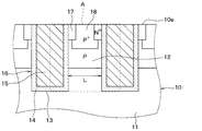
- the semiconductor device has a semiconductor substrate 10 constituting an N ⁇ -type drift layer 11.
- the semiconductor substrate 10 is formed of a silicon substrate.
- a P-type base layer 12 is formed on the drift layer 11 (that is, on the side of the surface 10 a of the semiconductor substrate 10).
- a plurality of trenches 13 are formed in the semiconductor substrate 10 so as to penetrate the base layer 12 and reach the drift layer 11.
- the base layer 12 is separated into a plurality.
- the plurality of trenches 13 are formed at equal intervals along one of the surface directions on one surface 10 a of the semiconductor substrate 10 (that is, the direction perpendicular to the sheet of FIG. It is done. That is, the trenches 13 are formed such that the intervals L between the adjacent trenches 13 are equal to each other.
- each trench 13 is formed such that the side surface is substantially parallel along the normal direction to the one surface 10 a of the semiconductor substrate 10.
- substantially parallel includes the case where the angle between the one surface 10 a of the semiconductor substrate 10 and the side surface of the trench 13 is about 85 °, in addition to the case of being completely parallel.
- a gate insulating film 14 is formed on the wall surface of each trench 13, and a gate electrode 15 is formed on the gate insulating film 14.
- the trench gate structure 16 is configured.
- the gate electrode 15 is formed to fill the inside of the trench 13.
- the gate insulating film 14 is formed of an oxide film, and is formed along the wall surface of the trench 13 with a uniform thickness of about 100 nm.
- the gate electrode 15 is made of polysilicon doped with an impurity.
- the gate electrode 15 is formed by depositing amorphous silicon by a CVD method and then heat treating it to crystallize the amorphous silicon into polysilicon, and the grain size of polysilicon is 50 to 1000 nm. There is.
- the impurity concentration of the N + -type emitter region 17 higher than that of the drift layer 11 and the base layer 12 is higher.
- P + -type contact regions 18 are respectively formed. Specifically, emitter region 17 is formed to terminate in base layer 12 and to be in contact with the side surface of trench 13. Further, the contact region 18 is formed to terminate in the base layer 12 in the same manner as the emitter region 17.
- emitter region 17 extends in a rod shape along the longitudinal direction of trench 13 so as to be in contact with the side surface of trench 13 in the region between trenches 13 and terminates inside the tip of trench 13 It is done. Further, the contact region 18 is sandwiched between the two emitter regions 17 and extends in a rod-like shape along the longitudinal direction of the trench 13 (that is, the emitter region 17).
- the contact region 18 of the present embodiment is formed deeper than the emitter region 17 with reference to the one surface 10 a of the semiconductor substrate 10.
- An interlayer insulating film 19 made of BPSG (abbreviation of Boron Phosphorus Silicon Glass) or the like is formed on one surface 10 a of the semiconductor substrate 10. Then, on the interlayer insulating film 19, an emitter electrode 20 electrically connected to the emitter region 17 and the contact region 18 (that is, the base layer 12) through the contact holes 19 a formed in the interlayer insulating film 19 is formed. It is done. In the present embodiment, the emitter electrode 20 corresponds to the first electrode.
- An N-type field stop layer (hereinafter referred to as “FS”) having an impurity concentration higher than that of the drift layer 11 on the opposite side of the drift layer 11 to the base layer 12 side (ie, the other surface 10 b side of the semiconductor substrate 10).
- a layer 21 is formed.
- this FS layer 21 is not necessarily required, the performance of withstand voltage and steady loss can be improved by preventing the spread of the depletion layer, and the injection amount of holes injected from the other surface 10b side of the semiconductor substrate 10 Prepared to control the
- a P-type collector layer 22 is formed on the opposite side to the drift layer 11 with the FS layer 21 interposed therebetween, and the collector layer 22 is electrically connected to the collector layer 22 (that is, the other surface 10b of the semiconductor substrate 10).
- Collector electrodes 23 connected to each other are formed. In the present embodiment, the collector electrode 23 corresponds to the second electrode.
- N-type, N + -type and N -- type correspond to the first conductivity type
- P-type and P + -type correspond to the second conductivity type.
- the semiconductor substrate 10 is configured to include the collector layer 22, the FS layer 21, the drift layer 11, the base layer 12, the emitter region 17, and the contact region 18.
- the above is the basic configuration of the semiconductor device in this embodiment. Next, the basic operation of the semiconductor device will be described.
- the emitter electrode 20 is grounded and a positive voltage is applied to the collector electrode 23. Then, a predetermined voltage is applied to the gate electrode 15 from a gate control circuit (not shown) so that the gate potential is equal to or higher than the threshold voltage Vth of the insulating gate structure.
- a gate control circuit not shown
- an N-type inversion layer i.e., a channel
- electrons are supplied from the emitter electrode 20 to the drift layer 11 through the emitter region 17 and the inversion layer.
- holes are supplied from the collector electrode 23 to the drift layer 11 through the collector layer 22. Then, in the semiconductor device, due to the conductivity modulation, the resistance value of the drift layer 11 is lowered to be turned on.
- a predetermined voltage for example, 0 V
- a gate control circuit not shown
- the inversion layer formed in the portion of base layer 12 in contact with trench 13 disappears, and electrons are not supplied from emitter electrode 20 and holes are not supplied from collector electrode 23. , Will be off.
- the stress around the trench means the stress generated when forming the gate electrode 15 as described above, but means the maximum stress among the stresses generated around the trench 13 doing.
- the stress around the trench in FIG. 2 is the maximum stress among the stress in the center of the semiconductor device, the trench 13 at the outer edge, the trench 13 between the center and the outer edge, etc. It shows the stress. That is, the stress around the trench in FIG. 2 indicates the maximum stress among the stresses around the trench 13 in the semiconductor device.
- the stress generated in the periphery of the trench 13 is in the region between the adjacent trenches 13 because the stress caused by each gate electrode 15 disposed in the adjacent trench 13 is applied together. The predetermined part of the area in between is the largest.
- the stress around the trench in FIG. 2 is a value analyzed by the EBSD (abbreviation of Electron Back Scatter Diffraction) method.
- the number of continuous switchings in FIG. 2 is one switching from turning off the semiconductor device to turning on the semiconductor device and turning the semiconductor device from the on state to the off state.
- the semiconductor device of the present embodiment is configured such that the stress around the trench is 340 MPa or less.
- FIG. 2 shows that the thickness of the semiconductor substrate 10 is 80 ⁇ m, the stress around the trench does not change even if the thickness of the semiconductor substrate 10 and the impurity concentration of each region are changed. That is, regardless of the thickness of the semiconductor substrate 10 and the impurity concentration of each region, destruction of the semiconductor device is suppressed if the stress around the trench is 340 MPa or less.
- the stress around the trench is due to the polysilicon constituting the gate electrode 15 as described above. More specifically, the trench ambient stress is due to thermal contraction during and after crystallization from amorphous silicon to polysilicon. Therefore, the stress around the trench can be changed by adjusting the amount of polysilicon forming the gate electrode 15.
- FIG. 3 is a cross section in which the extending direction of the trench 13 is a normal direction, and corresponds to an enlarged view around the trench gate structure 16 in FIG. Then, in the region from one surface 10a of semiconductor substrate 10 to the bottom of trench gate structure 16 in this cross section, the center of trench gate structure 16 to the center of trench gate structure 16 located next to the other across contact region 18 Assume that it is a one-cell area A.
- a region surrounded by one central axis of the adjacent trench gate structure 16 and the other central axis is one cell Region A That is, in the region from one surface 10a of semiconductor substrate 10 to the bottom of trench gate structure 16 in this cross section, it passes through the centers of adjacent trench gate structures 16 along the normal direction to one surface 10a of semiconductor substrate 10.
- An area surrounded by two virtual lines is referred to as one cell area A.
- a region surrounded by a dotted line is a one-cell region A.
- the bottom portion of the trench 13 is the portion farthest from the one surface 10 a of the semiconductor substrate 10 and is the bottom surface of the trench 13 in FIG. 3.
- the present inventors investigate based on the volume ratio of the gate electrode 15 (that is, polysilicon) per cell area A (hereinafter, also simply referred to as the volume ratio of the gate electrode 15), and the following results I got That is, as shown in FIG. 4, when the volume ratio of the gate electrode 15 is 41.5% or less, it was found that the stress around the trench was 340 MPa or less.
- the volume ratio of the gate electrode 15 is 41.5% or less.
- the total volume of the one cell region A may be increased by widening the interval L between the adjacent trenches 13. That is, in the present embodiment, by setting the distance L between the adjacent trenches 13 to 0.9 ⁇ m or more, the stress around the trench can be set to 340 MPa or less.
- the semiconductor device when the semiconductor device is in the on state, holes supplied to the drift layer 11 are more easily released to the base layer 12 as the distance L between the adjacent trenches 13 is increased.
- the on voltage increases.
- the semiconductor device in which the IGBT having the trench gate structure 16 as in this embodiment is formed it is currently desired that the on voltage be 0.9 V or less.
- the rate of change of the on voltage in the range where the distance 13 between adjacent trenches is wider than 1.3 ⁇ m is smaller than the rate of change of the on voltage in the range where the distance between adjacent trenches 13 is 1.3 ⁇ m or less.
- the distance between the adjacent trenches 13 when the distance between the adjacent trenches 13 is 1.3 ⁇ m or less, the on-state voltage becomes steep as the distance between the adjacent trenches becomes narrow. Therefore, in the present embodiment, the distance between adjacent trenches is 1.3 ⁇ m or less.
- the distance L between the adjacent trenches 13 means the narrowest part of the adjacent trenches 13.
- the volume ratio of the gate electrode 15 per cell area A is set to 41.5% or less so that the stress around the trench is 340 MPa or less. Therefore, destruction of the semiconductor device can be suppressed.
- the distance L between the adjacent trenches 13 is set to 1.3 ⁇ m or less. Therefore, it is possible to suppress the destruction of the semiconductor device while suppressing the increase of the on voltage.
- the present embodiment is the same as the first embodiment except that the configuration of the trench gate structure 16 is different from the first embodiment, and the other parts are the same as the first embodiment, and thus the description thereof is omitted here.
- the trench 13 is configured such that the first trench 13a located on the opening side and the second trench 13b located on the bottom side are in communication.
- the first trench 13 a is formed in the base layer 12, and the second trench 13 b reaches the drift layer 11 from near the interface between the base layer 12 and the drift layer 11 in the base layer 12. Is formed. That is, the second trench 13 b of the present embodiment is formed across the base layer 12 and the drift layer 11.
- the second trench 13b is substantially circular in shape with a portion in which the distance between the facing side surfaces is longer than the distance between the facing side surfaces of the first trench 13a in the cross section in FIG. That is, the trench 13 has a so-called wedge shape in the cross section in FIG.
- interval of the side which opposes is the length of the paper surface left-right direction in FIG. Further, in the present embodiment, since the spacing L between the adjacent trenches 13 is the spacing of the narrowest portion among the spacings of the neighboring trenches 13, the spacing of the narrowest portion among the spacings of the adjacent second trenches 13b. It becomes.
- the gate electrode 15 is formed on the wall surface of the trench 13 via the gate insulating film 14 so that the air gap 24 is formed inside.
- the gate electrode 15 is formed such that the air gap 24 is formed in the second trench 13 b.
- FIG. 7 is a cross section in which the extending direction of the trench 13 is a normal direction, and corresponds to an enlarged view around the trench gate structure 16 in FIG.
- one cell region A is a region surrounded by a dotted line in the figure. Includes the air gap 24.
- the stress at the time of forming the gate electrode 15 is relieved by the air gap 24. Therefore, in the present embodiment, as shown in FIG. 8, for example, when the volume ratio of the gate electrode 15 is 41.5%, the distance L between the adjacent trenches 13 may be about 0.6 ⁇ m.
- the distance L between the trenches 13 can be made shorter than in the first embodiment. Therefore, when the semiconductor device is in the on state, holes supplied to the drift layer 11 can be made difficult to escape through the base layer 12. That is, according to the present embodiment, it is possible to further reduce the on-voltage while suppressing the destruction of the semiconductor device.
- FIG. 8 is a simulation result when the volume ratio of the air gaps 24 per one cell region A is 8%. Therefore, for example, when the volume ratio of the gate electrode 15 is 41.5%, when the volume ratio of the air gaps 24 per cell area A is made larger than 8%, the distance L between the adjacent trenches 13 is further increased. It becomes short. On the other hand, in the case where the volume ratio of the gate electrode 15 is 41.5%, when the volume ratio of the air gaps 24 per cell area A is made smaller than 8%, the distance L between the adjacent trenches 13 becomes wide.
- the semiconductor substrate 10 in which the base layer 12 is formed on the drift layer 11 is prepared, and anisotropic etching such as reactive ion etching is performed to form the first trench 13 a.
- anisotropic etching such as reactive ion etching is performed to form the first trench 13 a.
- a mask for protecting the side surface of the first trench 13a is formed, and isotropic etching is performed on the bottom of the first trench 13a.
- a second trench 13b is formed which has a portion in which the distance between the opposite side surfaces is longer than the distance between the opposite side surfaces of the first trench 13a, and which is in communication with the first trench 13a.
- the gate insulating film 14 is formed by the CVD method, thermal oxidation or the like. Then, amorphous silicon is deposited on the gate insulating film 14 by the CVD method or the like, and then heat treatment is performed to crystallize the amorphous silicon into polysilicon to form the gate electrode 15.
- amorphous silicon is deposited by the CVD method, amorphous silicon is deposited almost uniformly on the gate insulating film 14. Therefore, when amorphous silicon is deposited by the CVD method, the first trench 13a is buried before the inside of the second trench 13b is completely buried, and the air gap 24 is formed in the second trench 13b.
- the air gap 24 is formed inside the gate electrode 15, and the stress when forming the gate electrode 15 is relaxed by the air gap 24. Therefore, for example, when the volume ratio of the gate electrode 15 is 41.5%, the distance L between the adjacent trenches 13 can be shortened as compared with the first embodiment. Therefore, the breakdown of the semiconductor device can be suppressed while suppressing the increase of the on voltage.
- the first conductivity type is N-type and the second conductivity type is P-type
- the first conductivity type is P-type
- the second conductivity type is N-type
- the following configuration may be employed in order to set the volume ratio of the gate electrode 15 to 41.5% or less while setting the distance L between the adjacent trenches 13 to less than 0.9 ⁇ m.
- the gate electrode 15 is formed along the wall surface of the trench 13, and the embedded film 25 is embedded inside the gate electrode 15, so that the volume ratio of the gate electrode 15 is 41.5%. It is good also as the following.
- the embedded film 25 is formed, for example, by depositing an oxide film by the CVD method or the like.
- the volume ratio of the gate electrode 15 may be 41.5% or less by thickening a portion of the gate insulating film 14 disposed on the bottom side of the trench 13. In the case of such a configuration, concentration of the electric field at the bottom of the trench 13 can also be suppressed.
- the buried film 26 may be formed on the side of the opening of the trench 13. That is, since the gate electrode 15 may be formed in a portion in contact with the base layer 12 via the gate insulating film 14, the gate electrode 15 is formed in the portion opposite to the emitter region 17 with the gate insulating film 14 interposed therebetween. You do not have to. Therefore, the volume ratio of the gate electrode 15 may be reduced by forming the buried film 26 on the opposite side to the emitter region 17 with the gate insulating film 14 interposed therebetween.
- the embedded film 26 is formed, for example, by depositing an oxide film by the CVD method or the like.
- each configuration may be combined respectively.
- the configuration of FIGS. 9 and 10 may be combined, and the portion of the gate insulating film 14 disposed on the bottom side of the trench 13 may be thickened while the embedded film 25 is disposed.
- the configuration of FIGS. 9 and 11 may be combined to include both the buried film 25 and the buried film 26.
- the configuration of FIGS. 10 and 11 may be combined to include the buried film 26 while thickening the portion of the gate insulating film 14 disposed on the bottom side of the trench 13. Then, all the configurations shown in FIGS. 9 to 11 may be combined to make the portion of the gate insulating film 14 disposed on the bottom side of the trench 13 thicker while providing the embedded film 25 and the embedded film 26.
- the semiconductor device may be a so-called RC (Reverse Conducting abbreviation) -IGBT in which an N-type cathode layer is formed together with the collector layer 22 on the other surface 10b side of the semiconductor substrate 10. .
- RC Reverse Conducting abbreviation
- the plurality of trenches 13 may have different spacings L between adjacent trenches. Even with such a configuration, the same effect as described above can be obtained as long as the stress that is the largest among the stresses around the trench is 340 MPa or less.
Abstract
This semiconductor device is provided with a semiconductor substrate (10) which comprises a drift layer (11), a base layer (12) that is arranged on the drift layer, and a collector layer (22) of a second conductivity type, which is formed on the opposite side of the base layer (12) with the drift layer (11) being sandwiched therebetween. This semiconductor device is also provided with a plurality of trench gate structures, each of which penetrates the base layer (12) and reaches the drift layer (11), while having a gate insulating film (14) which is formed on the wall surface of a trench (13) that extends in one direction in the surface direction of the semiconductor substrate (10) and a gate electrode (15) which is formed on the gate insulating film (14). The gate electrode (15) is configured from a polysilicon, so that the maximum stress generated around the trench (13) in the semiconductor substrate (10) is 340 MPa or less.
Description
本出願は、2017年11月3日に出願された日本特許出願番号2017-213329号に基づくもので、ここにその記載内容が参照により組み入れられる。
This application is based on Japanese Patent Application No. 2017-213329 filed on November 3, 2017, the contents of which are incorporated herein by reference.
本開示は、トレンチゲート型の絶縁ゲート型バイポーラトランジスタ(以下、単にIGBTという)が形成された半導体装置に関する。
The present disclosure relates to a semiconductor device in which a trench gate type insulated gate bipolar transistor (hereinafter simply referred to as an IGBT) is formed.
従来より、電力変換用半導体装置の1つとして、産業用モータ等の電子機器に使用されるIGBTが形成された半導体装置が知られている(例えば、特許文献1参照)。具体的には、この半導体装置では、N-型のドリフト層を構成する半導体基板の表層部にベース層が形成され、ベース層を貫通するように複数のトレンチが形成されている。そして、各トレンチは、ゲート絶縁膜およびゲート電極が順に形成されることで埋め込まれている。なお、ゲート絶縁膜は、酸化膜にて構成され、ゲート電極は、ポリシリコンにて構成されている。また、ベース層の表層部には、トレンチに接するようにN+型のエミッタ領域が形成され、半導体基板の他面側には、P+型のコレクタ層が形成されている。
そして、半導体基板の一面側には、ベース層およびエミッタ領域と電気的に接続されるエミッタ電極が形成されている。半導体基板の他面側には、コレクタ層と電気的に接続されるコレクタ電極が形成されている。 Conventionally, as one of semiconductor devices for power conversion, a semiconductor device in which an IGBT used for electronic equipment such as an industrial motor is formed is known (for example, see Patent Document 1). Specifically, in this semiconductor device, the base layer is formed on the surface layer portion of the semiconductor substrate constituting the N − -type drift layer, and a plurality of trenches are formed so as to penetrate the base layer. And each trench is embedded by forming a gate insulating film and a gate electrode in order. The gate insulating film is formed of an oxide film, and the gate electrode is formed of polysilicon. In the surface layer portion of the base layer, an N + -type emitter region is formed in contact with the trench, and a P + -type collector layer is formed on the other surface side of the semiconductor substrate.
An emitter electrode electrically connected to the base layer and the emitter region is formed on one side of the semiconductor substrate. A collector electrode electrically connected to the collector layer is formed on the other surface side of the semiconductor substrate.
このような半導体装置は、例えば、次のように製造される。すなわち、ドリフト層上にベース層を形成した後、ドリフト層に達するトレンチを形成する。次に、トレンチ内にゲート絶縁膜を形成する。そして、CVD(Chemical Vapor Depositionの略)法によって不純物がドープされたアモルファスシリコンを成膜する。続いて、熱処理を行うことにより、アモルファスシリコンをポリシリコンへと結晶化し、ポリシリコンによって構成されるゲート電極を形成する。その後は、一般的な半導体製造プロセスを行い、エミッタ領域、コレクタ層、エミッタ電極、コレクタ電極等を形成することによって上記半導体装置が製造される。
Such a semiconductor device is manufactured, for example, as follows. That is, after forming the base layer on the drift layer, a trench reaching the drift layer is formed. Next, a gate insulating film is formed in the trench. Then, amorphous silicon doped with impurities is formed into a film by a CVD (abbreviation of Chemical Vapor Deposition) method. Subsequently, heat treatment is performed to crystallize amorphous silicon into polysilicon, thereby forming a gate electrode made of polysilicon. Thereafter, the semiconductor device is manufactured by performing a general semiconductor manufacturing process and forming an emitter region, a collector layer, an emitter electrode, a collector electrode and the like.
しかしながら、上記半導体装置では、アモルファスシリコンをポリシリコンに結晶化する際、および結晶化した後の熱収縮により、ゲート電極の周囲に応力が発生する。つまり、半導体基板のうちのトレンチの周囲の領域に応力が発生する。そして、当該応力が大きいと、ゲート電極を構成するポリシリコン内に結晶欠陥が生成されたり、ゲート絶縁膜の劣化が促進したりし、半導体装置に電流を流した際に当該半導体装置が破壊されてしまう可能性がある。
However, in the above semiconductor device, stress is generated around the gate electrode due to crystallization of amorphous silicon to polysilicon and thermal contraction after crystallization. That is, stress is generated in the region around the trench in the semiconductor substrate. Then, if the stress is large, a crystal defect is generated in the polysilicon forming the gate electrode or deterioration of the gate insulating film is promoted, and the semiconductor device is broken when current flows through the semiconductor device. There is a possibility of
本開示は、破壊されることを抑制できる半導体装置を提供することを目的とする。
An object of the present disclosure is to provide a semiconductor device capable of suppressing destruction.
本開示の1つの観点によれば、半導体装置は、第1導電型のドリフト層と、ドリフト層上に配置された第2導電型のベース層と、ドリフト層を挟み、ベース層と反対側に形成された第2導電型のコレクタ層と、を有する半導体基板と、ベース層を貫通してドリフト層に達すると共に、半導体基板の面方向における一方向に延設されたトレンチの壁面に形成されたゲート絶縁膜と、ゲート絶縁膜上に形成されたゲート電極と、を有する複数のトレンチゲート構造と、ベース層の表層部に形成され、トレンチと接する第1導電型のエミッタ領域と、ベース層およびエミッタ領域と電気的に接続される第1電極と、コレクタ層と電気的に接続される第2電極と、を備えている。そして、ゲート電極は、ポリシリコンで構成されており、半導体基板におけるトレンチの周囲に発生している最大応力は、340MPa以下とされている。
According to one aspect of the present disclosure, a semiconductor device includes a drift layer of a first conductivity type, a base layer of a second conductivity type disposed on the drift layer, and the drift layer on the opposite side to the base layer. The semiconductor substrate having the formed second conductive type collector layer, and the drift layer through the base layer to reach the drift layer and formed on the wall surface of the trench extending in one direction in the surface direction of the semiconductor substrate A plurality of trench gate structures having a gate insulating film and a gate electrode formed on the gate insulating film, an emitter region of a first conductivity type formed in a surface layer portion of the base layer and in contact with the trench, a base layer A first electrode electrically connected to the emitter region, and a second electrode electrically connected to the collector layer. The gate electrode is made of polysilicon, and the maximum stress occurring around the trench in the semiconductor substrate is set to 340 MPa or less.
これによれば、トレンチの周囲に発生している最大応力が340MPa以下とされているため、半導体装置が破壊されることを抑制できる。
According to this, since the maximum stress occurring around the trench is set to 340 MPa or less, it is possible to suppress the semiconductor device from being broken.
なお、上記および特許請求の範囲における括弧内の符号は、特許請求の範囲に記載された用語と後述の実施形態に記載される当該用語を例示する具体物等との対応関係を示すものである。
Note that the reference numerals in parentheses in the above and the claims indicate the correspondence between the terms described in the claims and the concrete items and the like that exemplify the terms described in the embodiments described later. .
以下、本開示の実施形態について図に基づいて説明する。なお、以下の各実施形態相互において、互いに同一もしくは均等である部分には、同一符号を付して説明を行う。
Hereinafter, embodiments of the present disclosure will be described based on the drawings. In the following embodiments, parts that are the same as or equivalent to each other will be described with the same reference numerals.
(第1実施形態)
第1実施形態について説明する。なお、本実施形態の半導体装置は、例えば、インバータ、DC/DCコンバータ等の電源回路に使用されるパワースイッチング素子として利用されると好適である。 First Embodiment
The first embodiment will be described. The semiconductor device of the present embodiment is preferably used as a power switching element used in a power supply circuit such as an inverter or a DC / DC converter, for example.
図1に示されるように、半導体装置は、N-型のドリフト層11を構成する半導体基板10を有している。なお、本実施形態では、半導体基板10は、シリコン基板で構成される。そして、ドリフト層11上(すなわち、半導体基板10の一面10a側)には、P型のベース層12が形成されている。
As shown in FIG. 1, the semiconductor device has a semiconductor substrate 10 constituting an N − -type drift layer 11. In the present embodiment, the semiconductor substrate 10 is formed of a silicon substrate. Then, a P-type base layer 12 is formed on the drift layer 11 (that is, on the side of the surface 10 a of the semiconductor substrate 10).
半導体基板10には、ベース層12を貫通してドリフト層11に達するように複数のトレンチ13が形成されている。これにより、ベース層12が複数個に分離されている。本実施形態では、複数のトレンチ13は、ストライプ状となるように、半導体基板10の一面10aにおける面方向のうちの一方向(すなわち、図1中の紙面垂直方向)に沿って等間隔に形成されている。つまり、各トレンチ13は、隣接するトレンチ13の間隔Lが互いに等しくなるように形成されている。
A plurality of trenches 13 are formed in the semiconductor substrate 10 so as to penetrate the base layer 12 and reach the drift layer 11. Thus, the base layer 12 is separated into a plurality. In the present embodiment, the plurality of trenches 13 are formed at equal intervals along one of the surface directions on one surface 10 a of the semiconductor substrate 10 (that is, the direction perpendicular to the sheet of FIG. It is done. That is, the trenches 13 are formed such that the intervals L between the adjacent trenches 13 are equal to each other.
また、本実施形態では、各トレンチ13は、側面が半導体基板10の一面10aに対する法線方向に沿って略平行となるように形成されている。なお、ここでの略平行とは、完全に平行になる場合に加えて、半導体基板10の一面10aとトレンチ13の側面との成す角度が85°程度までのものを含むものである。
Further, in the present embodiment, each trench 13 is formed such that the side surface is substantially parallel along the normal direction to the one surface 10 a of the semiconductor substrate 10. Here, the term “substantially parallel” includes the case where the angle between the one surface 10 a of the semiconductor substrate 10 and the side surface of the trench 13 is about 85 °, in addition to the case of being completely parallel.
各トレンチ13の壁面には、ゲート絶縁膜14が形成され、ゲート絶縁膜14上には、ゲート電極15が形成されている。これにより、トレンチゲート構造16が構成されている。なお、本実施形態では、ゲート電極15は、トレンチ13内を埋め込むように形成されている。
A gate insulating film 14 is formed on the wall surface of each trench 13, and a gate electrode 15 is formed on the gate insulating film 14. Thus, the trench gate structure 16 is configured. In the present embodiment, the gate electrode 15 is formed to fill the inside of the trench 13.
ゲート絶縁膜14は、酸化膜で構成され、トレンチ13の壁面に沿って約100nmの均一な厚さで形成されている。ゲート電極15は、不純物がドープされたポリシリコンにて構成されている。なお、ゲート電極15は、CVD法でアモルファスシリコンが成膜された後、熱処理してアモルファスシリコンがポリシリコンへと結晶化されることで構成され、ポリシリコンの粒径が50~1000nmとされている。
The gate insulating film 14 is formed of an oxide film, and is formed along the wall surface of the trench 13 with a uniform thickness of about 100 nm. The gate electrode 15 is made of polysilicon doped with an impurity. The gate electrode 15 is formed by depositing amorphous silicon by a CVD method and then heat treating it to crystallize the amorphous silicon into polysilicon, and the grain size of polysilicon is 50 to 1000 nm. There is.
ベース層12の表層部(すなわち、半導体基板10の一面10a側)には、ドリフト層11よりも高不純物濃度とされたN+型のエミッタ領域17、およびベース層12よりも高不純物濃度とされたP+型のコンタクト領域18がそれぞれ形成されている。具体的には、エミッタ領域17は、ベース層12内において終端し、かつ、トレンチ13の側面に接するように形成されている。また、コンタクト領域18は、エミッタ領域17と同様に、ベース層12内において終端するように形成されている。
In the surface layer portion of the base layer 12 (ie, on the side of the surface 10 a of the semiconductor substrate 10), the impurity concentration of the N + -type emitter region 17 higher than that of the drift layer 11 and the base layer 12 is higher. P + -type contact regions 18 are respectively formed. Specifically, emitter region 17 is formed to terminate in base layer 12 and to be in contact with the side surface of trench 13. Further, the contact region 18 is formed to terminate in the base layer 12 in the same manner as the emitter region 17.
より詳しくは、エミッタ領域17は、トレンチ13間の領域において、トレンチ13の長手方向に沿ってトレンチ13の側面に接するように棒状に延設され、トレンチ13の先端よりも内側で終端する構造とされている。また、コンタクト領域18は、2つのエミッタ領域17に挟まれてトレンチ13の長手方向(すなわち、エミッタ領域17)に沿って棒状に延設されている。なお、本実施形態のコンタクト領域18は、半導体基板10の一面10aを基準としてエミッタ領域17よりも深く形成されている。
More specifically, emitter region 17 extends in a rod shape along the longitudinal direction of trench 13 so as to be in contact with the side surface of trench 13 in the region between trenches 13 and terminates inside the tip of trench 13 It is done. Further, the contact region 18 is sandwiched between the two emitter regions 17 and extends in a rod-like shape along the longitudinal direction of the trench 13 (that is, the emitter region 17). The contact region 18 of the present embodiment is formed deeper than the emitter region 17 with reference to the one surface 10 a of the semiconductor substrate 10.
半導体基板10の一面10a上には、BPSG(Boron Phosphorus Silicon Glassの略)等で構成される層間絶縁膜19が形成されている。そして、層間絶縁膜19上には、層間絶縁膜19に形成されたコンタクトホール19aを介してエミッタ領域17およびコンタクト領域18(すなわち、ベース層12)と電気的に接続されるエミッタ電極20が形成されている。なお、本実施形態では、エミッタ電極20が第1電極に相当している。
An interlayer insulating film 19 made of BPSG (abbreviation of Boron Phosphorus Silicon Glass) or the like is formed on one surface 10 a of the semiconductor substrate 10. Then, on the interlayer insulating film 19, an emitter electrode 20 electrically connected to the emitter region 17 and the contact region 18 (that is, the base layer 12) through the contact holes 19 a formed in the interlayer insulating film 19 is formed. It is done. In the present embodiment, the emitter electrode 20 corresponds to the first electrode.
ドリフト層11のうちのベース層12側と反対側(すなわち、半導体基板10の他面10b側)には、ドリフト層11よりも高不純物濃度とされたN型のフィールドストップ層(以下では、FS層という)21が形成されている。このFS層21は、必ずしも必要なものではないが、空乏層の広がりを防ぐことで耐圧と定常損失の性能向上を図ると共に、半導体基板10の他面10b側から注入される正孔の注入量を制御するために備えてある。
An N-type field stop layer (hereinafter referred to as “FS”) having an impurity concentration higher than that of the drift layer 11 on the opposite side of the drift layer 11 to the base layer 12 side (ie, the other surface 10 b side of the semiconductor substrate 10). A layer 21 is formed. Although this FS layer 21 is not necessarily required, the performance of withstand voltage and steady loss can be improved by preventing the spread of the depletion layer, and the injection amount of holes injected from the other surface 10b side of the semiconductor substrate 10 Prepared to control the
そして、FS層21を挟んでドリフト層11と反対側には、P型のコレクタ層22が形成され、コレクタ層22上(すなわち、半導体基板10の他面10b上)にはコレクタ層22と電気的に接続されるコレクタ電極23が形成されている。なお、本実施形態では、コレクタ電極23が第2電極に相当している。
Then, a P-type collector layer 22 is formed on the opposite side to the drift layer 11 with the FS layer 21 interposed therebetween, and the collector layer 22 is electrically connected to the collector layer 22 (that is, the other surface 10b of the semiconductor substrate 10). Collector electrodes 23 connected to each other are formed. In the present embodiment, the collector electrode 23 corresponds to the second electrode.
以上が本実施形態における半導体装置の基本的な構成である。なお、本実施形態では、N型、N+型、N-型が第1導電型に相当しており、P型、P+型が第2導電型に相当している。また、本実施形態では、半導体基板10は、上記のように、コレクタ層22、FS層21、ドリフト層11、ベース層12、エミッタ領域17、およびコンタクト領域18を含んで構成されている。
The above is the basic configuration of the semiconductor device in this embodiment. In the present embodiment, N-type, N + -type and N -- type correspond to the first conductivity type, and P-type and P + -type correspond to the second conductivity type. Further, in the present embodiment, as described above, the semiconductor substrate 10 is configured to include the collector layer 22, the FS layer 21, the drift layer 11, the base layer 12, the emitter region 17, and the contact region 18.
以上が本実施形態における半導体装置の基本的な構成である。次に、上記半導体装置の基本的な作動について説明する。
The above is the basic configuration of the semiconductor device in this embodiment. Next, the basic operation of the semiconductor device will be described.
まず、上記半導体装置は、オフ状態からオン状態にされる際、例えば、エミッタ電極20が接地されると共にコレクタ電極23に正の電圧が印加される。そして、ゲート電極15には、ゲート電位が絶縁ゲート構造の閾値電圧Vth以上となるように図示しないゲート制御回路から所定の電圧が印加される。これにより、半導体装置では、ベース層12のうちのトレンチ13と接する部分にN型の反転層(すなわち、チャネル)が形成される。そして、半導体装置では、エミッタ電極20からエミッタ領域17および反転層を介して電子がドリフト層11に供給される。また、半導体装置では、コレクタ電極23からコレクタ層22を介して正孔がドリフト層11に供給される。そして、半導体装置では、伝導度変調により、ドリフト層11の抵抗値が低下してオン状態となる。
First, when the semiconductor device is switched from the off state to the on state, for example, the emitter electrode 20 is grounded and a positive voltage is applied to the collector electrode 23. Then, a predetermined voltage is applied to the gate electrode 15 from a gate control circuit (not shown) so that the gate potential is equal to or higher than the threshold voltage Vth of the insulating gate structure. Thus, in the semiconductor device, an N-type inversion layer (i.e., a channel) is formed in a portion of the base layer 12 in contact with the trench 13. In the semiconductor device, electrons are supplied from the emitter electrode 20 to the drift layer 11 through the emitter region 17 and the inversion layer. In the semiconductor device, holes are supplied from the collector electrode 23 to the drift layer 11 through the collector layer 22. Then, in the semiconductor device, due to the conductivity modulation, the resistance value of the drift layer 11 is lowered to be turned on.
また、オン状態からオフ状態にされる際には、ゲート電極15には、ゲート電位が閾値電圧Vth未満となるように、図示しないゲート制御回路から所定の電圧(例えば、0V)が印加される。これにより、半導体装置では、ベース層12のうちのトレンチ13と接する部分に形成されていた反転層が消滅し、エミッタ電極20から電子が供給されなくなると共に、コレクタ電極23から正孔が供給されなくなり、オフ状態となる。
When the on state is changed to the off state, a predetermined voltage (for example, 0 V) is applied to the gate electrode 15 from a gate control circuit (not shown) such that the gate potential is less than the threshold voltage Vth. . Thereby, in the semiconductor device, the inversion layer formed in the portion of base layer 12 in contact with trench 13 disappears, and electrons are not supplied from emitter electrode 20 and holes are not supplied from collector electrode 23. , Will be off.
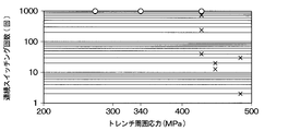
次に、トレンチ13の周囲に発生したトレンチ周囲応力と、半導体装置の破壊との関係について図2を参照しつつ説明する。なお、ここでのトレンチ周囲応力とは、上記のように、ゲート電極15を形成する際に発生する応力のことであるが、トレンチ13の周囲に発生した応力のうちの最大応力のことを意味している。また、図2中のトレンチ周囲応力は、半導体装置の中心に位置するトレンチ13、外縁部に位置するトレンチ13、中心と外縁部との間に位置するトレンチ13等の周囲の応力のうちの最大応力を示している。つまり、図2中のトレンチ周囲応力は、半導体装置におけるトレンチ13の周囲の応力のうちの最大応力を示している。また、トレンチ13の周囲に発生する応力は、隣接するトレンチ13の間の領域では当該隣接するトレンチ13に配置された各ゲート電極15に起因する応力が共に印加されるため、隣接するトレンチ13の間の領域の所定箇所が最大となる。
Next, the relationship between the trench surrounding stress generated around the trench 13 and the breakdown of the semiconductor device will be described with reference to FIG. Here, the stress around the trench means the stress generated when forming the gate electrode 15 as described above, but means the maximum stress among the stresses generated around the trench 13 doing. Also, the stress around the trench in FIG. 2 is the maximum stress among the stress in the center of the semiconductor device, the trench 13 at the outer edge, the trench 13 between the center and the outer edge, etc. It shows the stress. That is, the stress around the trench in FIG. 2 indicates the maximum stress among the stresses around the trench 13 in the semiconductor device. Further, the stress generated in the periphery of the trench 13 is in the region between the adjacent trenches 13 because the stress caused by each gate electrode 15 disposed in the adjacent trench 13 is applied together. The predetermined part of the area in between is the largest.
さらに、図2中のトレンチ周囲応力は、EBSD(Electron Back Scatter Diffractionの略)法で分析した値である。そして、図2中の連続スイッチング回数は、半導体装置をオフ状態からオン状態にし、オン状態からオフ状態にするまでを1回のスイッチングとしている。
Furthermore, the stress around the trench in FIG. 2 is a value analyzed by the EBSD (abbreviation of Electron Back Scatter Diffraction) method. The number of continuous switchings in FIG. 2 is one switching from turning off the semiconductor device to turning on the semiconductor device and turning the semiconductor device from the on state to the off state.
図2に示されるように、トレンチ周囲応力が340MPa以下の場合は、スイッチングを1000回行っても半導体装置が破壊されていないことが確認される。これに対し、トレンチ周囲応力が340MPaより大きい場合には、スイッチングを1000回行っても半導体装置が破壊されないことも確認されるが、スイッチングが1000回未満の回数で半導体装置が破壊されてしまうことも確認される。例えば、トレンチ周囲応力が420Mpaの場合には、1000回未満の回数で半導体装置が破壊されてしまうことが確認される。そして、トレンチ周囲応力がさらに大きくなると、例えば、トレンチ周囲応力が450MPaの場合には、十数回~数十回程度で半導体装置が破壊されてしまうことが確認される。つまり、トレンチ周囲応力が大きくなるほど、少ないスイッチング回数で半導体装置が破壊されてしまうことが確認される。このため、本実施形態の半導体装置は、トレンチ周囲応力が340MPa以下となるように構成されている。
As shown in FIG. 2, when the stress around the trench is 340 MPa or less, it is confirmed that the semiconductor device is not broken even if the switching is performed 1000 times. On the other hand, if the stress around the trench is greater than 340 MPa, it is also confirmed that the semiconductor device will not be destroyed even if switching is performed 1000 times, but the semiconductor device will be destroyed in less than 1000 switching times. Is also confirmed. For example, when the stress around trench is 420 MPa, it is confirmed that the semiconductor device is broken in less than 1000 times. When the stress around the trench is further increased, for example, when the stress around the trench is 450 MPa, it is confirmed that the semiconductor device is broken in about ten to several tens of times. That is, it is confirmed that as the stress around the trench becomes larger, the semiconductor device is broken at a smaller number of switching times. For this reason, the semiconductor device of the present embodiment is configured such that the stress around the trench is 340 MPa or less.
なお、図2は、半導体基板10の厚さを80μmとしたものであるが、半導体基板10の厚さや各領域の不純物濃度を変化させてもトレンチ周囲応力は変化しない。つまり、半導体基板10の厚さや各領域の不純物濃度に依らず、トレンチ周囲応力が340MPa以下であれば、半導体装置が破壊されることが抑制される。
Although FIG. 2 shows that the thickness of the semiconductor substrate 10 is 80 μm, the stress around the trench does not change even if the thickness of the semiconductor substrate 10 and the impurity concentration of each region are changed. That is, regardless of the thickness of the semiconductor substrate 10 and the impurity concentration of each region, destruction of the semiconductor device is suppressed if the stress around the trench is 340 MPa or less.
ここで、トレンチ周囲応力は、上記のようにゲート電極15を構成するポリシリコンに起因するものである。より具体的には、トレンチ周囲応力は、アモルファスシリコンからポリシリコンへと結晶化する際、および結晶化した後の熱収縮に起因するものである。このため、ゲート電極15を構成するポリシリコンの量を調整することにより、トレンチ周囲応力を変化させることができる。
Here, the stress around the trench is due to the polysilicon constituting the gate electrode 15 as described above. More specifically, the trench ambient stress is due to thermal contraction during and after crystallization from amorphous silicon to polysilicon. Therefore, the stress around the trench can be changed by adjusting the amount of polysilicon forming the gate electrode 15.
図3は、トレンチ13の延設方向を法線方向とする断面であり、図1中のトレンチゲート構造16周囲の拡大図に相当している。そして、この断面のうちの半導体基板10の一面10aからトレンチゲート構造16の底部までの領域において、トレンチゲート構造16の中心からコンタクト領域18を挟んで隣に位置するトレンチゲート構造16の中心までを1セル領域Aとする。言い換えると、この断面のうちの半導体基板10の一面10aからトレンチゲート構造16の底部までの領域において、隣接するトレンチゲート構造16の一方の中心軸と他方の中心軸とで囲まれる領域を1セル領域Aとする。つまり、この断面のうちの半導体基板10の一面10aからトレンチゲート構造16の底部までの領域において、隣接するトレンチゲート構造16の中心をそれぞれ通り、半導体基板10の一面10aに対する法線方向に沿った2つの仮想線で囲まれる領域を1セル領域Aとする。図3中では、点線で囲まれた領域が1セル領域Aとなる。なお、トレンチ13の底部とは、半導体基板10の一面10aから最も離れている部分のことであり、図3中ではトレンチ13の底面となる。
FIG. 3 is a cross section in which the extending direction of the trench 13 is a normal direction, and corresponds to an enlarged view around the trench gate structure 16 in FIG. Then, in the region from one surface 10a of semiconductor substrate 10 to the bottom of trench gate structure 16 in this cross section, the center of trench gate structure 16 to the center of trench gate structure 16 located next to the other across contact region 18 Assume that it is a one-cell area A. In other words, in a region from one surface 10a of semiconductor substrate 10 to the bottom of trench gate structure 16 in this cross section, a region surrounded by one central axis of the adjacent trench gate structure 16 and the other central axis is one cell Region A That is, in the region from one surface 10a of semiconductor substrate 10 to the bottom of trench gate structure 16 in this cross section, it passes through the centers of adjacent trench gate structures 16 along the normal direction to one surface 10a of semiconductor substrate 10. An area surrounded by two virtual lines is referred to as one cell area A. In FIG. 3, a region surrounded by a dotted line is a one-cell region A. The bottom portion of the trench 13 is the portion farthest from the one surface 10 a of the semiconductor substrate 10 and is the bottom surface of the trench 13 in FIG. 3.
そして、本発明者らは、1セル領域A当たりのゲート電極15(すなわち、ポリシリコン)の体積率(以下では、単にゲート電極15の体積率ともいう)に基づいて検討を行い、以下の結果を得た。すなわち、図4に示されるように、ゲート電極15の体積率が41.5%以下の場合、トレンチ周囲応力が340MPa以下となることを見出した。
Then, the present inventors investigate based on the volume ratio of the gate electrode 15 (that is, polysilicon) per cell area A (hereinafter, also simply referred to as the volume ratio of the gate electrode 15), and the following results I got That is, as shown in FIG. 4, when the volume ratio of the gate electrode 15 is 41.5% or less, it was found that the stress around the trench was 340 MPa or less.
このため、本実施形態では、ゲート電極15の体積率が41.5%以下とされている。なお、ゲート電極15の体積率を小さくするには、隣接するトレンチ13の間隔Lを広くすることによって1セル領域Aの総体積を増加させればよい。つまり、本実施形態では、隣接するトレンチ13の間隔Lを0.9μm以上とすることにより、トレンチ周囲応力を340MPa以下とできる。
Therefore, in the present embodiment, the volume ratio of the gate electrode 15 is 41.5% or less. In order to reduce the volume ratio of the gate electrode 15, the total volume of the one cell region A may be increased by widening the interval L between the adjacent trenches 13. That is, in the present embodiment, by setting the distance L between the adjacent trenches 13 to 0.9 μm or more, the stress around the trench can be set to 340 MPa or less.
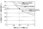
但し、図5に示されるように、半導体装置は、オン状態である際、隣接するトレンチ13の間隔Lを長くするほどドリフト層11に供給された正孔がベース層12へと抜けやすくなり、オン電圧が増加する。ここで、本実施形態のようなトレンチゲート構造16を有するIGBTが形成された半導体装置では、現状では、オン電圧が0.9V以下となるようにすることが望まれている。また、隣接するトレンチの間隔13が1.3μmより広い範囲におけるオン電圧の変化率は、隣接するトレンチ13の間隔が1.3μm以下である範囲のオン電圧の変化率より小さい。言い換えると、半導体装置は、隣接するトレンチ13の間隔が1.3μm以下の範囲では、隣接するトレンチの間隔が狭くなるにつれて急峻にオン電圧が小さくなる。このため、本実施形態では、隣接するトレンチの間隔が1.3μm以下とされている。なお、隣接するトレンチ13の間隔Lとは、隣接するトレンチ13のうちの最も間隔が狭い部分を意味している。
However, as shown in FIG. 5, when the semiconductor device is in the on state, holes supplied to the drift layer 11 are more easily released to the base layer 12 as the distance L between the adjacent trenches 13 is increased. The on voltage increases. Here, in the semiconductor device in which the IGBT having the trench gate structure 16 as in this embodiment is formed, it is currently desired that the on voltage be 0.9 V or less. Further, the rate of change of the on voltage in the range where the distance 13 between adjacent trenches is wider than 1.3 μm is smaller than the rate of change of the on voltage in the range where the distance between adjacent trenches 13 is 1.3 μm or less. In other words, in the semiconductor device, when the distance between the adjacent trenches 13 is 1.3 μm or less, the on-state voltage becomes steep as the distance between the adjacent trenches becomes narrow. Therefore, in the present embodiment, the distance between adjacent trenches is 1.3 μm or less. The distance L between the adjacent trenches 13 means the narrowest part of the adjacent trenches 13.
以上説明したように、本実施形態では、トレンチ周囲応力が340MPa以下となるように、1セル領域A当たりのゲート電極15の体積率を41.5%以下としている。このため、半導体装置が破壊されることを抑制できる。
As described above, in the present embodiment, the volume ratio of the gate electrode 15 per cell area A is set to 41.5% or less so that the stress around the trench is 340 MPa or less. Therefore, destruction of the semiconductor device can be suppressed.
また、隣接するトレンチ13の間隔Lは、1.3μm以下とされている。このため、オン電圧が増加することを抑制しつつ、半導体装置が破壊されることを抑制できる。
Further, the distance L between the adjacent trenches 13 is set to 1.3 μm or less. Therefore, it is possible to suppress the destruction of the semiconductor device while suppressing the increase of the on voltage.
(第2実施形態)
第2実施形態について説明する。本実施形態は、第1実施形態に対して、トレンチゲート構造16の構成を変更したものであり、その他に関しては第1実施形態と同様であるため、ここでは説明を省略する。 Second Embodiment
The second embodiment will be described. The present embodiment is the same as the first embodiment except that the configuration of thetrench gate structure 16 is different from the first embodiment, and the other parts are the same as the first embodiment, and thus the description thereof is omitted here.
第2実施形態について説明する。本実施形態は、第1実施形態に対して、トレンチゲート構造16の構成を変更したものであり、その他に関しては第1実施形態と同様であるため、ここでは説明を省略する。 Second Embodiment
The second embodiment will be described. The present embodiment is the same as the first embodiment except that the configuration of the
本実施形態では、図6に示されるように、トレンチ13は、開口部側に位置する第1トレンチ13aと、底部側に位置する第2トレンチ13bとが連通されて構成されている。本実施形態では、第1トレンチ13aは、ベース層12内に形成され、第2トレンチ13bは、ベース層12内のうちのベース層12とドリフト層11との界面付近からドリフト層11に達するように形成されている。つまり、本実施形態の第2トレンチ13bは、ベース層12からドリフト層11に渡って形成されている。
In the present embodiment, as shown in FIG. 6, the trench 13 is configured such that the first trench 13a located on the opening side and the second trench 13b located on the bottom side are in communication. In the present embodiment, the first trench 13 a is formed in the base layer 12, and the second trench 13 b reaches the drift layer 11 from near the interface between the base layer 12 and the drift layer 11 in the base layer 12. Is formed. That is, the second trench 13 b of the present embodiment is formed across the base layer 12 and the drift layer 11.
また、第2トレンチ13bは、図6中の断面において、対向する側面の間隔が第1トレンチ13aの対向する側面の間隔より長くなる部分を有する略円形状とされている。すなわち、トレンチ13は、図6中の断面においていわゆる壺形状とされている。
Further, the second trench 13b is substantially circular in shape with a portion in which the distance between the facing side surfaces is longer than the distance between the facing side surfaces of the first trench 13a in the cross section in FIG. That is, the trench 13 has a so-called wedge shape in the cross section in FIG.
なお、対向する側面の間隔とは、図6中の紙面左右方向の長さのことである。また、本実施形態では、隣接するトレンチ13の間隔Lは、隣接するトレンチ13の間隔のうちも最も狭い部分の間隔であるため、隣接する第2トレンチ13bの間隔のうちの最も狭い部分の間隔となる。
In addition, the space | interval of the side which opposes is the length of the paper surface left-right direction in FIG. Further, in the present embodiment, since the spacing L between the adjacent trenches 13 is the spacing of the narrowest portion among the spacings of the neighboring trenches 13, the spacing of the narrowest portion among the spacings of the adjacent second trenches 13b. It becomes.
そして、ゲート電極15は、内部に空隙24が形成されるように、トレンチ13の壁面にゲート絶縁膜14を介して形成されている。本実施形態では、第2トレンチ13b内に空隙24が形成されるように、ゲート電極15が形成されている。
The gate electrode 15 is formed on the wall surface of the trench 13 via the gate insulating film 14 so that the air gap 24 is formed inside. In the present embodiment, the gate electrode 15 is formed such that the air gap 24 is formed in the second trench 13 b.
以上が本実施形態における半導体装置の構成である。次に、本実施形態のゲート電極15の体積率について図7を参照しつつ説明する。図7は、トレンチ13の延設方向を法線方向とする断面であり、図6中のトレンチゲート構造16周囲の拡大図に相当している。
The above is the configuration of the semiconductor device in this embodiment. Next, the volume ratio of the gate electrode 15 of the present embodiment will be described with reference to FIG. FIG. 7 is a cross section in which the extending direction of the trench 13 is a normal direction, and corresponds to an enlarged view around the trench gate structure 16 in FIG.
本実施形態では、図7に示されるように、トレンチ13の延設方向を法線方向とする断面において、1セル領域Aは、図中の点線で囲まれた領域となり、1セル領域A内には空隙24が含まれる。そして、ゲート電極15を形成する際の応力は、空隙24にて緩和される。したがって、本実施形態では、図8に示されるように、例えば、ゲート電極15の体積率を41.5%とする場合、隣接するトレンチ13の間隔Lが約0.6μmであればよく、隣接するトレンチ13の間隔Lを上記第1実施形態よりも短くできる。このため、半導体装置がオン状態である際において、ドリフト層11に供給された正孔がベース層12を介して抜け難くできる。すなわち、本実施形態によれば、半導体装置が破壊されることを抑制しつつ、さらにオン電圧の低減を図ることもできる。
In the present embodiment, as shown in FIG. 7, in a cross section in which the extending direction of the trench 13 is a normal direction, one cell region A is a region surrounded by a dotted line in the figure. Includes the air gap 24. The stress at the time of forming the gate electrode 15 is relieved by the air gap 24. Therefore, in the present embodiment, as shown in FIG. 8, for example, when the volume ratio of the gate electrode 15 is 41.5%, the distance L between the adjacent trenches 13 may be about 0.6 μm. The distance L between the trenches 13 can be made shorter than in the first embodiment. Therefore, when the semiconductor device is in the on state, holes supplied to the drift layer 11 can be made difficult to escape through the base layer 12. That is, according to the present embodiment, it is possible to further reduce the on-voltage while suppressing the destruction of the semiconductor device.
なお、図8は、1セル領域A当たりの空隙24の体積率を8%とした際のシミュレーション結果である。このため、例えば、ゲート電極15の体積率を41.5%とする場合、1セル領域A当たりの空隙24の体積率を8%より大きくなるようにすると、隣接するトレンチ13の間隔Lがさらに短くなる。反対に、ゲート電極15の体積率を41.5%とする場合、1セル領域A当たりの空隙24の体積率を8%より小さくなるようにすると、隣接するトレンチ13の間隔Lが広くなる。
FIG. 8 is a simulation result when the volume ratio of the air gaps 24 per one cell region A is 8%. Therefore, for example, when the volume ratio of the gate electrode 15 is 41.5%, when the volume ratio of the air gaps 24 per cell area A is made larger than 8%, the distance L between the adjacent trenches 13 is further increased. It becomes short. On the other hand, in the case where the volume ratio of the gate electrode 15 is 41.5%, when the volume ratio of the air gaps 24 per cell area A is made smaller than 8%, the distance L between the adjacent trenches 13 becomes wide.
次に、このような半導体装置の製造方法について簡単に説明する。このような半導体装置は、ドリフト層11上にベース層12が形成された半導体基板10を用意し、反応性イオンエッチング等の異方性エッチングを行って第1トレンチ13aを形成する。次に、第1トレンチ13aの側面を保護するマスクを形成し、第1トレンチ13aの底面に対して等方性エッチングを行う。これにより、対向する側面の間隔が第1トレンチ13aの対向する側面の間隔より長くなる部分を有し、第1トレンチ13aと連通する第2トレンチ13bが形成される。
Next, a method of manufacturing such a semiconductor device will be briefly described. In such a semiconductor device, the semiconductor substrate 10 in which the base layer 12 is formed on the drift layer 11 is prepared, and anisotropic etching such as reactive ion etching is performed to form the first trench 13 a. Next, a mask for protecting the side surface of the first trench 13a is formed, and isotropic etching is performed on the bottom of the first trench 13a. Thus, a second trench 13b is formed which has a portion in which the distance between the opposite side surfaces is longer than the distance between the opposite side surfaces of the first trench 13a, and which is in communication with the first trench 13a.
その後、CVD法や熱酸化等によりゲート絶縁膜14を形成する。そして、ゲート絶縁膜14上に、CVD法等でアモルファスシリコンを成膜した後、熱処理することでアモルファスシリコンをポリシリコンへ結晶化させてゲート電極15を構成する。なお、CVD法でアモルファスシリコンを成膜する際、アモルファスシリコンはゲート絶縁膜14上にほぼ均一に成膜される。このため、CVD法によりアモルファスシリコンを成膜すると、第2トレンチ13b内が完全に埋め込まれる前に第1トレンチ13aが埋め込まれ、第2トレンチ13b内に空隙24が形成された状態となる。
Thereafter, the gate insulating film 14 is formed by the CVD method, thermal oxidation or the like. Then, amorphous silicon is deposited on the gate insulating film 14 by the CVD method or the like, and then heat treatment is performed to crystallize the amorphous silicon into polysilicon to form the gate electrode 15. When amorphous silicon is deposited by the CVD method, amorphous silicon is deposited almost uniformly on the gate insulating film 14. Therefore, when amorphous silicon is deposited by the CVD method, the first trench 13a is buried before the inside of the second trench 13b is completely buried, and the air gap 24 is formed in the second trench 13b.
その後は、従来の一般的な半導体装置の製造プロセスを行い、エミッタ領域17、コンタクト領域18、層間絶縁膜19、エミッタ電極20、FS層21、コレクタ層22、コレクタ電極23等を適宜形成することにより、上記半導体装置が製造される。
Thereafter, a conventional general semiconductor device manufacturing process is performed to appropriately form emitter region 17, contact region 18, interlayer insulating film 19, emitter electrode 20, FS layer 21, collector layer 22, collector electrode 23 and the like. Thus, the above-described semiconductor device is manufactured.
以上説明したように、本実施形態では、ゲート電極15の内部に空隙24が形成されており、ゲート電極15を形成する際の応力が当該空隙24にて緩和される構成となっている。このため、上記第1実施形態と比較して、例えば、ゲート電極15の体積率を41.5%とする場合、隣接するトレンチ13の間隔Lを短くできる。したがって、さらにオン電圧が増加することを抑制しつつ、半導体装置が破壊されることを抑制できる。
As described above, in the present embodiment, the air gap 24 is formed inside the gate electrode 15, and the stress when forming the gate electrode 15 is relaxed by the air gap 24. Therefore, for example, when the volume ratio of the gate electrode 15 is 41.5%, the distance L between the adjacent trenches 13 can be shortened as compared with the first embodiment. Therefore, the breakdown of the semiconductor device can be suppressed while suppressing the increase of the on voltage.
(他の実施形態)
本開示は、実施形態に準拠して記述されたが、本開示は当該実施形態や構造に限定されるものではないと理解される。本開示は、様々な変形例や均等範囲内の変形をも包含する。加えて、様々な組み合わせや形態、さらには、それらに一要素のみ、それ以上、あるいはそれ以下、を含む他の組み合わせや形態をも、本開示の範疇や思想範囲に入るものである。 (Other embodiments)
Although the present disclosure has been described in accordance with the embodiment, it is understood that the present disclosure is not limited to the embodiment or the structure. The present disclosure also includes various modifications and variations within the equivalent range. In addition, various combinations and forms, and further, other combinations and forms including only one element, or more or less than these elements are also within the scope and the scope of the present disclosure.
例えば、上記第1実施形態では、第1導電型をN型とし、第2導電型をP型とした例について説明したが、第1導電型をP型とし、第2導電型をN型とすることもできる。
For example, in the first embodiment, an example in which the first conductivity type is N-type and the second conductivity type is P-type has been described, but the first conductivity type is P-type and the second conductivity type is N-type You can also
また、上記第1実施形態において、隣接するトレンチ13の間隔Lを0.9μm未満としつつ、ゲート電極15の体積率を41.5%以下とするために以下の構成としてもよい。例えば、図9に示されるように、ゲート電極15をトレンチ13の壁面に沿って形成し、ゲート電極15の内部に埋込膜25を埋め込むことにより、ゲート電極15の体積率を41.5%以下としてもよい。なお、埋込膜25は、例えば、CVD法等で酸化膜を成膜することによって形成される。
In the first embodiment, the following configuration may be employed in order to set the volume ratio of the gate electrode 15 to 41.5% or less while setting the distance L between the adjacent trenches 13 to less than 0.9 μm. For example, as shown in FIG. 9, the gate electrode 15 is formed along the wall surface of the trench 13, and the embedded film 25 is embedded inside the gate electrode 15, so that the volume ratio of the gate electrode 15 is 41.5%. It is good also as the following. The embedded film 25 is formed, for example, by depositing an oxide film by the CVD method or the like.
さらに、図10に示されるように、ゲート絶縁膜14のうちのトレンチ13の底部側に配置される部分を厚くすることにより、ゲート電極15の体積率を41.5%以下としてもよい。なお、このような構成とした場合には、トレンチ13の底部にて電界が集中することも抑制できる。
Furthermore, as shown in FIG. 10, the volume ratio of the gate electrode 15 may be 41.5% or less by thickening a portion of the gate insulating film 14 disposed on the bottom side of the trench 13. In the case of such a configuration, concentration of the electric field at the bottom of the trench 13 can also be suppressed.
また、図11に示されるように、トレンチ13の開口部側に埋込膜26を形成するようにしてもよい。つまり、ゲート電極15は、ゲート絶縁膜14を介してベース層12と接する部分に形成されていればよいため、ゲート絶縁膜14を挟んでエミッタ領域17と反対側に位置する部分には形成されていなくてもよい。このため、ゲート絶縁膜14を挟んでエミッタ領域17と反対側に埋込膜26を形成することにより、ゲート電極15の体積率を小さくするようにしてもよい。なお、埋込膜26は、例えば、CVD法等で酸化膜を成膜することによって形成される。
Further, as shown in FIG. 11, the buried film 26 may be formed on the side of the opening of the trench 13. That is, since the gate electrode 15 may be formed in a portion in contact with the base layer 12 via the gate insulating film 14, the gate electrode 15 is formed in the portion opposite to the emitter region 17 with the gate insulating film 14 interposed therebetween. You do not have to. Therefore, the volume ratio of the gate electrode 15 may be reduced by forming the buried film 26 on the opposite side to the emitter region 17 with the gate insulating film 14 interposed therebetween. The embedded film 26 is formed, for example, by depositing an oxide film by the CVD method or the like.
また、特に図示しないが、各構成をそれぞれ組み合わせてもよい。例えば、図9および図10の構成を組み合わせ、埋込膜25を配置しつつ、ゲート絶縁膜14のうちのトレンチ13の底部側に配置される部分を厚くしてもよい。また、図9および図11の構成を組み合わせ、埋込膜25と埋込膜26を共に備える構成としてもよい。さらに、図10および図11の構成を組み合わせ、ゲート絶縁膜14のうちのトレンチ13の底部側に配置される部分を厚くしつつ、埋込膜26を備える構成としてもよい。そして、図9~図11の構成を全て組み合わせ、埋込膜25および埋込膜26を備えつつ、ゲート絶縁膜14のうちのトレンチ13の底部側に配置される部分を厚くしてもよい。
Further, although not particularly illustrated, each configuration may be combined respectively. For example, the configuration of FIGS. 9 and 10 may be combined, and the portion of the gate insulating film 14 disposed on the bottom side of the trench 13 may be thickened while the embedded film 25 is disposed. Further, the configuration of FIGS. 9 and 11 may be combined to include both the buried film 25 and the buried film 26. Furthermore, the configuration of FIGS. 10 and 11 may be combined to include the buried film 26 while thickening the portion of the gate insulating film 14 disposed on the bottom side of the trench 13. Then, all the configurations shown in FIGS. 9 to 11 may be combined to make the portion of the gate insulating film 14 disposed on the bottom side of the trench 13 thicker while providing the embedded film 25 and the embedded film 26.
さらに、上記各実施形態において、半導体基板10の他面10b側に、コレクタ層22と共にN型のカソード層が形成された、いわゆるRC(Reverse Conductingの略)-IGBTとされた半導体装置としてもよい。
Furthermore, in each of the above embodiments, the semiconductor device may be a so-called RC (Reverse Conducting abbreviation) -IGBT in which an N-type cathode layer is formed together with the collector layer 22 on the other surface 10b side of the semiconductor substrate 10. .
また、上記各実施形態において、複数のトレンチ13は、隣接するトレンチの間隔Lが異なっていてもよい。このような構成としても、トレンチ周囲応力のうちも最も大きくなる応力が340MPa以下であれば、上記と同様の効果を得ることができる。
In each of the above embodiments, the plurality of trenches 13 may have different spacings L between adjacent trenches. Even with such a configuration, the same effect as described above can be obtained as long as the stress that is the largest among the stresses around the trench is 340 MPa or less.
Claims (4)
- 複数のトレンチゲート構造(16)を有する半導体装置であって、
第1導電型のドリフト層(11)と、
前記ドリフト層上に配置された第2導電型のベース層(12)と、
前記ドリフト層を挟み、前記ベース層と反対側に形成された第2導電型のコレクタ層(22)と、を有する半導体基板(10)と、
前記ベース層を貫通して前記ドリフト層に達すると共に、前記半導体基板の面方向における一方向に延設されたトレンチ(13)の壁面に形成されたゲート絶縁膜(14)と、前記ゲート絶縁膜上に形成されたゲート電極(15)と、を有する前記複数のトレンチゲート構造と、
前記ベース層の表層部に形成され、前記トレンチと接する第1導電型のエミッタ領域(17)と、
前記ベース層および前記エミッタ領域と電気的に接続される第1電極(20)と、
前記コレクタ層と電気的に接続される第2電極(23)と、を備え、
前記ゲート電極は、ポリシリコンで構成されており、
前記半導体基板における前記トレンチの周囲に発生している最大応力は、340MPa以下とされている半導体装置。 A semiconductor device having a plurality of trench gate structures (16), comprising:
A drift layer (11) of the first conductivity type,
A second conductivity type base layer (12) disposed on the drift layer;
A semiconductor substrate (10) having a collector layer (22) of the second conductivity type formed on the side opposite to the base layer, sandwiching the drift layer;
A gate insulating film (14) formed on a wall surface of a trench (13) extending through the base layer to reach the drift layer and extending in one direction in the surface direction of the semiconductor substrate; A plurality of trench gate structures having a gate electrode (15) formed thereon;
An emitter region (17) of a first conductivity type formed in a surface layer portion of the base layer and in contact with the trench;
A first electrode (20) electrically connected to the base layer and the emitter region;
A second electrode (23) electrically connected to the collector layer;
The gate electrode is made of polysilicon,
The semiconductor device whose maximum stress occurring around the trench in the semiconductor substrate is 340 MPa or less. - 前記トレンチの延設方向を法線方向とする断面において、前記半導体基板の一面(10a)と前記トレンチゲート構造の底部との間の領域のうち、隣接する前記トレンチゲート構造の一方の中心軸と他方の中心軸とで囲まれる領域を1セル領域(A)とすると、前記1セル領域に占める前記ゲート電極の体積率が41.5%以下とされている請求項1に記載の半導体装置。 In a cross section in which the extending direction of the trench is a normal direction, one central axis of the adjacent trench gate structure in an area between one surface (10a) of the semiconductor substrate and the bottom of the trench gate structure is 2. The semiconductor device according to claim 1, wherein a volume ratio of the gate electrode occupying the one cell region is 41.5% or less, where a region surrounded by the other central axis is a one cell region (A).
- 隣接する前記トレンチの間隔(L)は、1.3μm以下とされている請求項1または2に記載の半導体装置。 The semiconductor device according to claim 1, wherein a distance (L) between the adjacent trenches is 1.3 μm or less.
- 前記ゲート電極は、内部に空隙(24)が形成されている請求項1ないし3のいずれか1つに記載の半導体装置。 The semiconductor device according to any one of claims 1 to 3, wherein the gate electrode has an air gap (24) formed therein.
Priority Applications (2)
| Application Number | Priority Date | Filing Date | Title |
|---|---|---|---|
| CN201880071034.6A CN111295765B (en) | 2017-11-03 | 2018-11-01 | Semiconductor device with a plurality of semiconductor chips |
| US16/862,790 US11508836B2 (en) | 2017-11-03 | 2020-04-30 | Semiconductor device including trench gate structure with specific volume ratio of gate electrodes |
Applications Claiming Priority (2)
| Application Number | Priority Date | Filing Date | Title |
|---|---|---|---|
| JP2017-213329 | 2017-11-03 | ||
| JP2017213329A JP7009933B2 (en) | 2017-11-03 | 2017-11-03 | Semiconductor device |
Related Child Applications (1)
| Application Number | Title | Priority Date | Filing Date |
|---|---|---|---|
| US16/862,790 Continuation US11508836B2 (en) | 2017-11-03 | 2020-04-30 | Semiconductor device including trench gate structure with specific volume ratio of gate electrodes |
Publications (1)
| Publication Number | Publication Date |
|---|---|
| WO2019088241A1 true WO2019088241A1 (en) | 2019-05-09 |
Family
ID=66333276
Family Applications (1)
| Application Number | Title | Priority Date | Filing Date |
|---|---|---|---|
| PCT/JP2018/040772 WO2019088241A1 (en) | 2017-11-03 | 2018-11-01 | Semiconductor device |
Country Status (4)
| Country | Link |
|---|---|
| US (1) | US11508836B2 (en) |
| JP (1) | JP7009933B2 (en) |
| CN (1) | CN111295765B (en) |
| WO (1) | WO2019088241A1 (en) |
Citations (5)
| Publication number | Priority date | Publication date | Assignee | Title |
|---|---|---|---|---|
| JP2006114853A (en) * | 2004-10-18 | 2006-04-27 | Toshiba Corp | Semiconductor device and manufacturing method thereof |
| JP2007088010A (en) * | 2005-09-20 | 2007-04-05 | Denso Corp | Semiconductor device and its manufacturing method |
| JP2013251397A (en) * | 2012-05-31 | 2013-12-12 | Denso Corp | Semiconductor device |
| WO2015019862A1 (en) * | 2013-08-06 | 2015-02-12 | 富士電機株式会社 | Trench gate mos semiconductor device and method for manufacturing same |
| JP2015213163A (en) * | 2014-04-15 | 2015-11-26 | ローム株式会社 | Semiconductor device and manufacturing method of semiconductor device |
Family Cites Families (11)
| Publication number | Priority date | Publication date | Assignee | Title |
|---|---|---|---|---|
| JP2874062B2 (en) * | 1991-02-25 | 1999-03-24 | 松下電子工業株式会社 | Method for manufacturing thin film transistor |
| TW442972B (en) * | 1999-10-01 | 2001-06-23 | Anpec Electronics Corp | Fabricating method of trench-type gate power metal oxide semiconductor field effect transistor |
| US7217950B2 (en) * | 2002-10-11 | 2007-05-15 | Nissan Motor Co., Ltd. | Insulated gate tunnel-injection device having heterojunction and method for manufacturing the same |
| JP4534500B2 (en) * | 2003-05-14 | 2010-09-01 | 株式会社デンソー | Manufacturing method of semiconductor device |
| JP2007005723A (en) * | 2005-06-27 | 2007-01-11 | Toshiba Corp | Semiconductor device |
| JP2007043123A (en) | 2005-07-01 | 2007-02-15 | Toshiba Corp | Semiconductor device |
| JP5609939B2 (en) * | 2011-09-27 | 2014-10-22 | 株式会社デンソー | Semiconductor device |
| JP6459791B2 (en) * | 2014-07-14 | 2019-01-30 | 株式会社デンソー | Semiconductor device and manufacturing method thereof |
| JP2014232895A (en) | 2014-09-11 | 2014-12-11 | 株式会社村田製作所 | Multilayer ceramic capacitor |
| KR102509260B1 (en) * | 2015-11-20 | 2023-03-14 | 삼성디스플레이 주식회사 | Polishing slurry for silicon, method of polishing polysilicon and method of manufacturing a thin film transistor substrate |
| US10643852B2 (en) * | 2016-09-30 | 2020-05-05 | Semiconductor Components Industries, Llc | Process of forming an electronic device including exposing a substrate to an oxidizing ambient |
-
2017
- 2017-11-03 JP JP2017213329A patent/JP7009933B2/en active Active
-
2018
- 2018-11-01 CN CN201880071034.6A patent/CN111295765B/en active Active
- 2018-11-01 WO PCT/JP2018/040772 patent/WO2019088241A1/en active Application Filing
-
2020
- 2020-04-30 US US16/862,790 patent/US11508836B2/en active Active
Patent Citations (5)
| Publication number | Priority date | Publication date | Assignee | Title |
|---|---|---|---|---|
| JP2006114853A (en) * | 2004-10-18 | 2006-04-27 | Toshiba Corp | Semiconductor device and manufacturing method thereof |
| JP2007088010A (en) * | 2005-09-20 | 2007-04-05 | Denso Corp | Semiconductor device and its manufacturing method |
| JP2013251397A (en) * | 2012-05-31 | 2013-12-12 | Denso Corp | Semiconductor device |
| WO2015019862A1 (en) * | 2013-08-06 | 2015-02-12 | 富士電機株式会社 | Trench gate mos semiconductor device and method for manufacturing same |
| JP2015213163A (en) * | 2014-04-15 | 2015-11-26 | ローム株式会社 | Semiconductor device and manufacturing method of semiconductor device |
Also Published As
| Publication number | Publication date |
|---|---|
| JP7009933B2 (en) | 2022-01-26 |
| CN111295765A (en) | 2020-06-16 |
| JP2019087591A (en) | 2019-06-06 |
| CN111295765B (en) | 2023-04-18 |
| US20200312986A1 (en) | 2020-10-01 |
| US11508836B2 (en) | 2022-11-22 |
Similar Documents
| Publication | Publication Date | Title |
|---|---|---|
| JP5196766B2 (en) | Semiconductor device | |
| JP5985624B2 (en) | Insulated gate transistor and method of manufacturing the same | |
| JP5482886B2 (en) | Semiconductor device | |
| JP6226786B2 (en) | Semiconductor device and manufacturing method thereof | |
| JP2009043966A (en) | Semiconductor apparatus and method of manufacturing the same | |
| JP2015118966A (en) | Semiconductor device | |
| WO2013080806A1 (en) | Insulated gate semiconductor device and method for manufacturing same | |
| JP6509673B2 (en) | Semiconductor device | |
| JP6807390B2 (en) | Semiconductor devices and their manufacturing methods | |
| JP6471508B2 (en) | Semiconductor device | |
| JP2010135677A (en) | Semiconductor device | |
| KR20150101895A (en) | Semiconductor device | |
| JP2016115847A (en) | Semiconductor device | |
| JPWO2019049572A1 (en) | Silicon carbide semiconductor device and method of manufacturing silicon carbide semiconductor device | |
| JP2006332199A (en) | SiC SEMICONDUCTOR DEVICE | |
| JP6681238B2 (en) | Semiconductor device and method of manufacturing semiconductor device | |
| US10748988B2 (en) | Semiconductor device | |
| JP6771433B2 (en) | Semiconductor device | |
| WO2019088241A1 (en) | Semiconductor device | |
| JP2010093080A (en) | Semiconductor device | |
| JP2013055177A (en) | Semiconductor device and method of manufacturing the same | |
| CN102222619B (en) | Semiconductor device manufacturing method | |
| US20150364585A1 (en) | Power semiconductor device | |
| JP2014192191A (en) | Semiconductor device and semiconductor device manufacturing method | |
| JP6265619B2 (en) | Power semiconductor device and manufacturing method thereof |
Legal Events
| Date | Code | Title | Description |
|---|---|---|---|
| 121 | Ep: the epo has been informed by wipo that ep was designated in this application |
Ref document number: 18874128 Country of ref document: EP Kind code of ref document: A1 |
|
| NENP | Non-entry into the national phase |
Ref country code: DE |
|
| 122 | Ep: pct application non-entry in european phase |
Ref document number: 18874128 Country of ref document: EP Kind code of ref document: A1 |