JP2006332199A - SiC SEMICONDUCTOR DEVICE - Google Patents
SiC SEMICONDUCTOR DEVICE Download PDFInfo
- Publication number
- JP2006332199A JP2006332199A JP2005151373A JP2005151373A JP2006332199A JP 2006332199 A JP2006332199 A JP 2006332199A JP 2005151373 A JP2005151373 A JP 2005151373A JP 2005151373 A JP2005151373 A JP 2005151373A JP 2006332199 A JP2006332199 A JP 2006332199A
- Authority
- JP
- Japan
- Prior art keywords
- sic
- electrode film
- region
- conductive region
- semiconductor layer
- Prior art date
- Legal status (The legal status is an assumption and is not a legal conclusion. Google has not performed a legal analysis and makes no representation as to the accuracy of the status listed.)
- Pending
Links
Images


Abstract
Description
本発明は、SiCを主組成とする半導体層を備えており、電気特性の改善を図ったSiC半導体装置に関する。 The present invention relates to a SiC semiconductor device that includes a semiconductor layer mainly composed of SiC and has improved electrical characteristics.
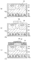
SiCは、絶縁破壊電界が高く、従来のSi半導体装置では実現できなかった高耐圧、超低損失の半導体装置の実現を目指した研究開発が活発に行われている。図8は、従来のSiC半導体装置の断面構造を示している。以下、図8を参照し、従来のSiC半導体装置の構造を説明する。図8に示されるSiC半導体装置2はMOSFETである。SiC半導体装置2において、高濃度のN型不純物を含むN+バルク層201はN+型SiC基板を構成している。このN+バルク層201は、対向する主面201aおよび201bを備えている。N+バルク層201の主面201a上には、N+バルク層201よりも不純物濃度の低いN型SiCを含むN−ドリフト層202が形成されている。
SiC has a high dielectric breakdown electric field, and research and development aiming at realization of a semiconductor device having a high breakdown voltage and an ultra-low loss that could not be realized by a conventional Si semiconductor device is being actively conducted. FIG. 8 shows a cross-sectional structure of a conventional SiC semiconductor device. Hereinafter, the structure of a conventional SiC semiconductor device will be described with reference to FIG. The
N−ドリフト層202の表面領域には、P型SiCを含むP型ウェル203が形成されている。P型ウェル203の表面領域には、N−ドリフト層202よりも不純物濃度の高いN型SiCを含むN+ソース領域204が形成されている。P型ウェル203およびN−ドリフト層202上には、ゲート酸化膜205が形成されており、ゲート酸化膜205上にはゲート電極膜206が形成されている。ゲート電極膜206はゲート端子Gに接続されている。ゲート酸化膜205およびゲート電極膜206上には層間絶縁膜207が形成されており、ゲート電極膜206は、ゲート酸化膜205および層間絶縁膜207によって周囲の構造から絶縁されている。
A P-
層間絶縁膜207にはコンタクトホールが設けられ、そのコンタクトホール内にはN+ソース領域204とオーミック接触を形成するソース電極膜208が形成されている。ソース電極膜208はソース端子Sに接続されている。N+バルク層201の主面201b上には、N+バルク層201とオーミック接触を形成するドレイン電極膜209が形成されている。ドレイン電極膜209はドレイン端子Dに接続されている。
A contact hole is provided in the
従来、電気特性の向上を図ったSiC半導体装置が開示されている。例えば、特許文献1には、高耐圧化を図ったSiCダイオードが記載されている。また、特許文献2には、逆方向漏れ電流の低減を図ったSiCショットキーバリアダイオードが記載されている。
従来のSiC−MOSFETにおいて、チップコストを低くするため、定格電流値での電流密度が、Si−MOSFETの数倍に設計される。このため、定格電流値を超えて電流が流れる順方向サージが加わった場合に、電流値が同じでも、発生する熱量は、SiC−MOSFETの方がSi−MOSFETよりも大きくなる。順方向サージに伴う発熱によって、素子が破壊されることもあり、従来のSiC−MOSFETにおいては、順方向サージに対する耐性がSi−MOSFETよりも低いという問題があった。 In the conventional SiC-MOSFET, in order to reduce the chip cost, the current density at the rated current value is designed to be several times that of the Si-MOSFET. For this reason, when a forward surge in which a current flows exceeding the rated current value is applied, even if the current value is the same, the amount of heat generated is larger in the SiC-MOSFET than in the Si-MOSFET. The element may be destroyed due to heat generated by the forward surge, and the conventional SiC-MOSFET has a problem that resistance to the forward surge is lower than that of the Si-MOSFET.
本発明は、上述した問題点に鑑みてなされたものであって、順方向サージに対する耐性を向上することができるSiC半導体装置を提供することを目的とする。 The present invention has been made in view of the above-described problems, and an object of the present invention is to provide a SiC semiconductor device capable of improving resistance to a forward surge.
本発明は、上記の課題を解決するためになされたもので、請求項1に記載の発明は、対向する第1および第2の主面を備え、第1導電型のSiCを含む第1の半導体層と、前記第1の主面上に形成された、前記第1の半導体層よりも不純物濃度の低い第1導電型のSiCを含む第2の半導体層と、前記第2の半導体層の表面領域に形成された、第2導電型のSiCを含む第1の導電領域と、前記第1の導電領域の表面領域に形成された、前記第2の半導体層よりも不純物濃度の高い第1導電型のSiCを含む第2の導電領域と、絶縁膜を隔てて前記第1の導電領域および前記第2の導電領域の一部と隣接するゲート電極膜と、前記第2の導電領域上に形成された第1の電極膜と、前記第1の半導体層において、前記第2の主面側の表面領域に形成された、第2導電型のSiCを含む第3の導電領域と、前記第1の半導体層上および前記第3の導電領域上に形成された第2の電極膜とを有することを特徴とするSiC半導体装置である。
The present invention has been made to solve the above-described problems, and the invention according to
請求項2に記載の発明は、対向する第1および第2の主面を備え、第1導電型のSiCを含む第1の半導体層と、前記第1の主面上に形成された、前記第1の半導体層よりも不純物濃度の低い第1導電型のSiCを含む第2の半導体層と、前記第2の半導体層の表面領域に形成された、第2導電型のSiCを含む第1の導電領域と、前記第1の導電領域の表面領域に形成された、前記第2の半導体層よりも不純物濃度の高い第1導電型のSiCを含む第2の導電領域と、絶縁膜を隔てて前記第1の導電領域および前記第2の導電領域の一部と隣接するゲート電極膜と、前記第2の導電領域上に形成された第1の電極膜と、前記第1の半導体層において、前記第2の主面側の表面領域に形成された、第2導電型のSiCを含む第3の導電領域と、前記第1の半導体層上に形成された第2の電極膜と、前記第3の導電領域上に形成され、前記第3の導電領域とオーミック接触を形成する第3の電極膜とを有することを特徴とするSiC半導体装置である。 According to a second aspect of the present invention, there is provided a first semiconductor layer including first and second main surfaces facing each other, including a first conductivity type SiC, and the first semiconductor surface formed on the first main surface. A second semiconductor layer containing SiC of a first conductivity type having a lower impurity concentration than the first semiconductor layer; and a first semiconductor containing SiC of a second conductivity type formed in a surface region of the second semiconductor layer. The insulating region is separated from the second conductive region containing SiC of the first conductivity type having a higher impurity concentration than the second semiconductor layer formed in the surface region of the first conductive region. A gate electrode film adjacent to a part of the first conductive region and the second conductive region, a first electrode film formed on the second conductive region, and the first semiconductor layer. A third conductive region containing SiC of the second conductivity type formed in the surface region on the second main surface side; A second electrode film formed on the first semiconductor layer; and a third electrode film formed on the third conductive region and forming an ohmic contact with the third conductive region. The SiC semiconductor device characterized by the above.
本発明によれば、第1の半導体層の表面領域に、第1の半導体層と反対の導電型の第3の半導体層を形成することによって、順方向サージが印加されても、第2の半導体層が伝導度変調され、オン抵抗が低下し、発熱量が低下するので、順方向サージに対する耐性を向上することができるという効果が得られる。 According to the present invention, by forming a third semiconductor layer having a conductivity type opposite to the first semiconductor layer in the surface region of the first semiconductor layer, even if a forward surge is applied, the second semiconductor layer is formed. The conductivity of the semiconductor layer is modulated, the on-resistance is reduced, and the amount of heat generation is reduced, so that the effect of improving the resistance to forward surge can be obtained.
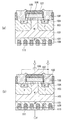
以下、図面を参照し、本発明を実施するための最良の形態について説明する。図1は、本発明の第1の実施形態によるSiC半導体装置の断面構造を示している。以下、図1を参照し、本実施形態によるSiC半導体装置の構造を説明する。図1に示される半導体装置1aはMOSFETである。SiC半導体装置1aにおいて、高濃度のN型不純物を含むN+バルク層101はN+型SiC基板を構成している。このN+バルク層101は、対向する主面101aおよび101bを備えている。N+バルク層101の主面101a上には、N+バルク層101よりも不純物濃度の低いN型SiCを含むN−ドリフト層102が形成されている。
The best mode for carrying out the present invention will be described below with reference to the drawings. FIG. 1 shows a cross-sectional structure of the SiC semiconductor device according to the first embodiment of the present invention. The structure of the SiC semiconductor device according to the present embodiment will be explained below with reference to FIG. The
N−ドリフト層102の表面領域には、P型SiCを含むP型ウェル103が形成されている。P型ウェル103の表面領域には、N−ドリフト層102よりも不純物濃度の高いN型SiCを含むN+ソース領域104が形成されている。P型ウェル103およびN−ドリフト層102上には、ゲート酸化膜105が形成されており、ゲート酸化膜105上には、例えばP(リン)を含んだポリシリコンからなるゲート電極膜106が形成されている。ゲート電極膜106はゲート端子Gに接続されている。ゲート酸化膜105およびゲート電極膜106上には、例えばリンガラス(PSG:Phospho Silicate Glass)からなる層間絶縁膜107が形成されており、ゲート電極膜106は、ゲート酸化膜105および層間絶縁膜107によって周囲の構造から絶縁されている。
A P-type well 103 containing P-type SiC is formed in the surface region of the N − drift layer 102. In the surface region of the P-
層間絶縁膜107にはコンタクトホールが設けられており、そのコンタクトホール内には、N+ソース領域104とオーミック接触を形成する、例えばNi(ニッケル)あるいはTi(チタン)からなるソース電極膜108が形成されている。ソース電極膜108はソース端子Sに接続されている。N+バルク層101において、主面101b側の表面領域には、高濃度のP型不純物を含むSiCを主組成としたP型領域109が形成されている。P型領域109は複数領域に分かれて形成されており、主面101b側から見て露出したN+バルク層101とP型領域109とが交互に繰り返される構造となっている。P型領域109は、イオン注入によって形成されており、P型領域109の内部および近傍には適度に結晶欠陥が発生している。N+バルク層101の主面101b上には、N+バルク層101とオーミック接触を形成する、例えばNiからなるドレイン電極膜110が形成されている。ドレイン電極膜110はドレイン端子Dに接続されている。ドレイン電極膜110を構成する材料は、P型領域109ともオーミック接触を形成する材料であることが望ましい。
A contact hole is provided in the
ソース電極膜108を接地し、ドレイン電極膜110に正電圧を印加し、ゲート電極膜106に正電圧を印加すると、ドレイン電極膜110からソース電極膜108へ向かって電流が流れる。このとき、ゲート電極膜106の下にあるP型ウェル103の表面にチャネルが形成され、N+ソース領域104中の電子がこのチャネルを通ってN−ドリフト層102に流れ込む。また、ドレイン電極膜110に印加された電圧を増加していくと、P型領域109とN+バルク層101との間のPN接合が順バイアスされ、P型領域109からN+バルク層101を通ってN−ドリフト層102にホールが流れ込む。ホールの注入により、N−ドリフト層102が伝導度変調される。
When the
これによって、N−ドリフト層102のオン抵抗が大きく下がるので、順方向に電流が流れやすくなる。半導体装置1aの電流−電圧特性は、図2に示されるようになり、ドレイン電極膜110に印加された正電圧(ドレイン電圧)が、ある電圧値以上になると、電流−電圧特性はIGBT(Insulated Gate Bipolar Transistor)のような特性を示し、従来構造よりもより多くの電流が流れるようになる。上記のように、N+バルク層101の表面領域に、N+バルク層101と反対の導電型のP型領域109を形成することによって、従来構造よりも低電圧でより多くの電流を流すことができるので、順方向サージが加わった場合の発熱量を低減し、順方向サージに対する耐性を向上することができる。なお、図2に示される特性は一例であり、これに限定されるわけではない。
As a result, the on-resistance of the N − drift layer 102 is greatly reduced, so that a current easily flows in the forward direction. The current-voltage characteristic of the
P型領域109を形成する際のイオン注入によって、P型領域109の内部および近傍には結晶欠陥が発生している。高濃度に不純物が注入された結果、P型領域109の内部および近傍のダメージは激しく、熱処理を行っても、適度に結晶欠陥が残っている。半導体装置1aの動作時には、P型領域109、N+バルク層101、N−ドリフト層102、およびP型ウェル103からなるPNP内蔵トランジスタが形成されている。通常、この内蔵トランジスタにおいては、ベース層として機能するN+バルク層101から注入される電子を中性化するように、エミッタ層として機能するP型領域109からP型ウェル103へ向かって、ホール電流が流れる。P型領域109の内部および近傍に結晶欠陥に起因した準位が存在すると、この準位を介して、N+バルク層101の電子とP型領域109のホールが再結合してしまうため、結晶欠陥が存在しない場合よりも内蔵トランジスタの電流増幅率は小さい。そのため、内蔵トランジスタの動作によって大電流が流れ続けるラッチアップを防止することができる。
Due to ion implantation when forming the P-
次に、本実施形態による半導体装置1aの製造方法を、図3〜図5を参照して説明する。直列抵抗を下げる低抵抗のN+バルク層101(不純物濃度は、例えば5×1019cm−3である)の主面101a上に、耐圧を確保するために必要な不純物濃度と厚さを持つ高抵抗のN−ドリフト層102を、CVD(Chemical Vapor Deposition)法等によって形成する。N−ドリフト層102の不純物濃度は、例えば5×1015cm−3であり、膜厚は、例えば10μmである(図3(a))。
Next, the method for fabricating the
このN−ドリフト層102にAl(アルミニウム)もしくはB(ボロン)をイオン注入し、反転チャネルを形成するためのP型ウェル103を形成する。P型ウェル103の不純物濃度は、N−ドリフト層102の不純物濃度に応じて決定する必要があり、本実施形態においては、例えば1×1016cm−3であるとする。イオン注入時の注入エネルギーは、例えば500〜3000keVであり、P型ウェル103の深さは、例えば0.5〜3μmである。さらに、P型ウェル103にP(リン)もしくはN(窒素)をイオン注入して、MOSFETのソース領域として作用させるためのN+ソース領域104を形成する。N+ソース領域104の不純物濃度は、例えば1×1019cm−3である(図3(b))。
Al (aluminum) or B (boron) ions are implanted into this N − drift layer 102 to form a P-type well 103 for forming an inversion channel. The impurity concentration of the P-type well 103 needs to be determined according to the impurity concentration of the N − drift layer 102, and is assumed to be, for example, 1 × 10 16 cm −3 in the present embodiment. The implantation energy at the time of ion implantation is, for example, 500 to 3000 keV, and the depth of the P-
続いて、N+バルク層101に主面101b側からAlもしくはBをイオン注入し、順方向サージ印加時に少数キャリアを供給するP型領域109を形成する。P型領域109の不純物濃度は、例えば2×1019cm−3以上である。イオン注入時の注入エネルギーは、例えば500〜3000keVであり、P型領域109の厚さは、例えば0.5〜3μmである。さらに、1500℃以上の熱処理を施し、P型ウェル103、N+ソース領域104、およびP型領域109に注入された不純物を活性化させる(図3(c))。
Subsequently, Al or B ions are implanted into the N + bulk layer 101 from the
続いて、高温のガス中で熱酸化を行い、ゲート酸化膜105を形成する。酸化膜の一部は裏面酸化膜105aとなる。この熱酸化において、ガス種としてO2,NO,NO2等を用いることができる(図4(a))。熱酸化の際に、N+バルク層101の主面101b上で酸化膜が成長することによって、P型領域109の一部が酸化膜となって消費されてしまうことを防ぐため、熱酸化の前にCVD法等によって酸化膜を主面101b上に予め形成してもよい。
Subsequently, thermal oxidation is performed in a high-temperature gas to form a
続いて、ゲート酸化膜105上に、CVD法等によって、Pを多く含んだポリシリコンを堆積し、ポリシリコン膜をパターニングして、ゲート電極膜106を形成する(図4(b))。さらに、CVD法等によってリンガラス(PSG)をゲート酸化膜105およびゲート電極膜106上に堆積し、層間絶縁膜107を形成する(図4(c))。
Subsequently, polysilicon containing a large amount of P is deposited on the
続いて、フッ酸を含む酸を用いた酸処理によって裏面酸化膜105aを除去する。さらに、ドライエッチング等によって層間絶縁膜107にコンタクトホールを形成し、P型ウェル103の表面の一部およびN+ソース領域104の表面を露出させる。このコンタクトホールの表面に、電子ビーム蒸着法等によってNiあるいはTi等の金属膜を堆積した後、酸処理によって金属膜をパターニングし、ソース電極膜108を形成する(図5(a))。
Subsequently, the
続いて、電子ビーム蒸着法等によって、N+バルク層101の主面101b上にNi等の金属膜を堆積し、ドレイン電極膜110を形成する。さらに、900℃以上の熱処理を施すことによって、N+ソース領域104−ソース電極膜108間およびN+バルク層101−ドレイン電極膜110間にオーミック接触が形成される。上述した工程を経て、半導体装置1aが完成する(図5(b))。
Subsequently, a metal film such as Ni is deposited on the
次に、本発明の第2の実施形態を説明する。図6は、本実施形態による半導体装置の断面構造を示している。図6に示される半導体装置1bにおいて、第1の実施形態による半導体装置1aと同一の構造には同一の符号が付与されている。半導体装置1bにおいては、N+バルク層101の主面101b上に、P型領域109とオーミック接触を形成するP型領域電極膜111が形成されている。P型領域電極膜111は、例えばTiおよびAlの積層膜である。P型領域電極膜111を設けたことによって、P型領域109とP型領域電極膜111との間に十分なオーミック接触を得ることができ、第1の実施形態による半導体装置1aと比べて、順方向サージ印加時に少数キャリアの注入がより起こりやすくなって、より電流が流れやすくなるため、順方向サージに対する耐性をより向上することができる。
Next, a second embodiment of the present invention will be described. FIG. 6 shows a cross-sectional structure of the semiconductor device according to the present embodiment. In the
以下、本実施形態による半導体装置1bの製造方法を説明する。製造工程の途中までは、第1の実施形態と同様である(図3〜図5(a))。図5(a)に示されるようにソース電極膜108を形成した後、電子ビーム蒸着法等によってN+バルク層101の主面101b上にTiおよびAlをこの順で堆積して金属膜を形成する。金属膜のうち、P型領域109上の部分を残して他の部分を除去するように金属膜のパターニングを行い、P型領域電極膜111を形成する(図7(a))。
The method for manufacturing the
続いて、電子ビーム蒸着法等によって、N+バルク層101の主面101bおよびP型領域電極膜111上にNi等の金属膜を堆積し、ドレイン電極膜110を形成する。さらに、900℃以上の熱処理を施すことによって、N+ソース領域104−ソース電極膜108間、N+バルク層101−ドレイン電極膜110間、およびP型領域109−P型領域電極膜111間にオーミック接触が形成される。上述した工程を経て、半導体装置1bが完成する(図7(b))。
Subsequently, a metal film such as Ni is deposited on the
以上、図面を参照して本発明の実施形態について詳述してきたが、具体的な構成はこれらの実施形態に限られるものではなく、この発明の要旨を逸脱しない範囲の設計変更等も含まれる。 As described above, the embodiments of the present invention have been described in detail with reference to the drawings. However, the specific configuration is not limited to these embodiments, and includes design changes and the like without departing from the gist of the present invention. .
1a,1b,2・・・半導体装置、101,201・・・N+バルク層、101a,101b,201a,201b・・・主面、102,202・・・N−ドリフト層、103,203・・・P型ウェル、104,204・・・N+ソース領域、105,205・・・ゲート酸化膜、106,206・・・ゲート電極膜、107,207・・・層間絶縁膜、108,208・・・ソース電極膜、109・・・P型領域、110,209・・・ドレイン電極膜、111・・・P型領域電極膜 1a, 1b, 2 · · · semiconductor device, 101, 201 · · · N + bulk layer, 101a, 101b, 201a, 201b · · · main surface, 102, 202 · · · N - drift layer, 103, 203, .. P-type well, 104, 204... N + source region, 105, 205... Gate oxide film, 106, 206... Gate electrode film, 107, 207. ... Source electrode film, 109 ... P-type region, 110,209 ... Drain electrode film, 111 ... P-type region electrode film
Claims (2)
前記第1の主面上に形成された、前記第1の半導体層よりも不純物濃度の低い第1導電型のSiCを含む第2の半導体層と、
前記第2の半導体層の表面領域に形成された、第2導電型のSiCを含む第1の導電領域と、
前記第1の導電領域の表面領域に形成された、前記第2の半導体層よりも不純物濃度の高い第1導電型のSiCを含む第2の導電領域と、
絶縁膜を隔てて前記第1の導電領域および前記第2の導電領域の一部と隣接するゲート電極膜と、
前記第2の導電領域上に形成された第1の電極膜と、
前記第1の半導体層において、前記第2の主面側の表面領域に形成された、第2導電型のSiCを含む第3の導電領域と、
前記第1の半導体層上および前記第3の導電領域上に形成された第2の電極膜と、
を有することを特徴とするSiC半導体装置。 A first semiconductor layer comprising opposing first and second major surfaces and comprising SiC of a first conductivity type;
A second semiconductor layer including SiC of a first conductivity type formed on the first main surface and having an impurity concentration lower than that of the first semiconductor layer;
A first conductive region formed in a surface region of the second semiconductor layer and containing SiC of a second conductivity type;
A second conductive region containing SiC of a first conductivity type formed in a surface region of the first conductive region and having an impurity concentration higher than that of the second semiconductor layer;
A gate electrode film adjacent to a part of the first conductive region and the second conductive region across an insulating film;
A first electrode film formed on the second conductive region;
A third conductive region containing SiC of the second conductivity type formed in the surface region on the second main surface side in the first semiconductor layer;
A second electrode film formed on the first semiconductor layer and on the third conductive region;
A SiC semiconductor device comprising:
前記第1の主面上に形成された、前記第1の半導体層よりも不純物濃度の低い第1導電型のSiCを含む第2の半導体層と、
前記第2の半導体層の表面領域に形成された、第2導電型のSiCを含む第1の導電領域と、
前記第1の導電領域の表面領域に形成された、前記第2の半導体層よりも不純物濃度の高い第1導電型のSiCを含む第2の導電領域と、
絶縁膜を隔てて前記第1の導電領域および前記第2の導電領域の一部と隣接するゲート電極膜と、
前記第2の導電領域上に形成された第1の電極膜と、
前記第1の半導体層において、前記第2の主面側の表面領域に形成された、第2導電型のSiCを含む第3の導電領域と、
前記第1の半導体層上に形成された第2の電極膜と、
前記第3の導電領域上に形成され、前記第3の導電領域とオーミック接触を形成する第3の電極膜と、
を有することを特徴とするSiC半導体装置。
A first semiconductor layer comprising opposing first and second major surfaces and comprising SiC of a first conductivity type;
A second semiconductor layer including SiC of a first conductivity type formed on the first main surface and having an impurity concentration lower than that of the first semiconductor layer;
A first conductive region formed in a surface region of the second semiconductor layer and containing SiC of a second conductivity type;
A second conductive region containing SiC of a first conductivity type formed in a surface region of the first conductive region and having an impurity concentration higher than that of the second semiconductor layer;
A gate electrode film adjacent to a part of the first conductive region and the second conductive region across an insulating film;
A first electrode film formed on the second conductive region;
A third conductive region containing SiC of the second conductivity type formed in the surface region on the second main surface side in the first semiconductor layer;
A second electrode film formed on the first semiconductor layer;
A third electrode film formed on the third conductive region and forming an ohmic contact with the third conductive region;
A SiC semiconductor device comprising:
Priority Applications (1)
| Application Number | Priority Date | Filing Date | Title |
|---|---|---|---|
| JP2005151373A JP2006332199A (en) | 2005-05-24 | 2005-05-24 | SiC SEMICONDUCTOR DEVICE |
Applications Claiming Priority (1)
| Application Number | Priority Date | Filing Date | Title |
|---|---|---|---|
| JP2005151373A JP2006332199A (en) | 2005-05-24 | 2005-05-24 | SiC SEMICONDUCTOR DEVICE |
Publications (1)
| Publication Number | Publication Date |
|---|---|
| JP2006332199A true JP2006332199A (en) | 2006-12-07 |
Family
ID=37553602
Family Applications (1)
| Application Number | Title | Priority Date | Filing Date |
|---|---|---|---|
| JP2005151373A Pending JP2006332199A (en) | 2005-05-24 | 2005-05-24 | SiC SEMICONDUCTOR DEVICE |
Country Status (1)
| Country | Link |
|---|---|
| JP (1) | JP2006332199A (en) |
Cited By (8)
| Publication number | Priority date | Publication date | Assignee | Title |
|---|---|---|---|---|
| JP2012156207A (en) * | 2011-01-24 | 2012-08-16 | Mitsubishi Electric Corp | Semiconductor device and method of manufacturing the same |
| JP2013232556A (en) * | 2012-04-27 | 2013-11-14 | National Institute Of Advanced Industrial & Technology | Silicon carbide semiconductor element manufacturing method |
| WO2013190907A1 (en) * | 2012-06-21 | 2013-12-27 | 住友電気工業株式会社 | Silicon carbide semiconductor device |
| WO2014128839A1 (en) * | 2013-02-20 | 2014-08-28 | 株式会社 日立製作所 | Semiconductor device and power conversion device using same |
| CN110767753A (en) * | 2019-11-13 | 2020-02-07 | 电子科技大学 | SiC power device |
| CN111524970A (en) * | 2020-01-09 | 2020-08-11 | 杭州电子科技大学 | 4H-SiC groove insulated gate bipolar transistor |
| JP2021019044A (en) * | 2019-07-18 | 2021-02-15 | 株式会社デンソー | Switching element |
| CN112687743A (en) * | 2020-12-29 | 2021-04-20 | 电子科技大学 | Groove type silicon carbide reverse resistance MOSFET device and preparation method thereof |
Citations (10)
| Publication number | Priority date | Publication date | Assignee | Title |
|---|---|---|---|---|
| JPS60170263A (en) * | 1984-02-15 | 1985-09-03 | Nec Corp | Vertical type field-effect transistor |
| JPS6180857A (en) * | 1984-09-28 | 1986-04-24 | Hitachi Ltd | Semiconductor switching device |
| JPS61121758A (en) * | 1984-11-13 | 1986-06-09 | デイジタル イクイプメント コーポレーシヨン | Brushless direct current motor |
| JPS6248073A (en) * | 1985-08-27 | 1987-03-02 | Mitsubishi Electric Corp | Semiconductor device |
| JPS6489564A (en) * | 1987-09-30 | 1989-04-04 | Nec Corp | Semiconductor device |
| JPH0414263A (en) * | 1990-05-07 | 1992-01-20 | Fuji Electric Co Ltd | Insulated gate type bipolar transistor |
| JPH098301A (en) * | 1995-04-20 | 1997-01-10 | Toshiba Corp | Power semiconductor device |
| JP2000012846A (en) * | 1998-06-22 | 2000-01-14 | Denso Corp | Silicon carbide semiconductor device and manufacture thereof |
| JP2001313393A (en) * | 2000-04-28 | 2001-11-09 | Toshiba Corp | Semiconductor device for power and method of driving the same |
| JP2004146679A (en) * | 2002-10-25 | 2004-05-20 | Toyota Central Res & Dev Lab Inc | Bipolar type semiconductor device and its manufacturing method |
-
2005
- 2005-05-24 JP JP2005151373A patent/JP2006332199A/en active Pending
Patent Citations (10)
| Publication number | Priority date | Publication date | Assignee | Title |
|---|---|---|---|---|
| JPS60170263A (en) * | 1984-02-15 | 1985-09-03 | Nec Corp | Vertical type field-effect transistor |
| JPS6180857A (en) * | 1984-09-28 | 1986-04-24 | Hitachi Ltd | Semiconductor switching device |
| JPS61121758A (en) * | 1984-11-13 | 1986-06-09 | デイジタル イクイプメント コーポレーシヨン | Brushless direct current motor |
| JPS6248073A (en) * | 1985-08-27 | 1987-03-02 | Mitsubishi Electric Corp | Semiconductor device |
| JPS6489564A (en) * | 1987-09-30 | 1989-04-04 | Nec Corp | Semiconductor device |
| JPH0414263A (en) * | 1990-05-07 | 1992-01-20 | Fuji Electric Co Ltd | Insulated gate type bipolar transistor |
| JPH098301A (en) * | 1995-04-20 | 1997-01-10 | Toshiba Corp | Power semiconductor device |
| JP2000012846A (en) * | 1998-06-22 | 2000-01-14 | Denso Corp | Silicon carbide semiconductor device and manufacture thereof |
| JP2001313393A (en) * | 2000-04-28 | 2001-11-09 | Toshiba Corp | Semiconductor device for power and method of driving the same |
| JP2004146679A (en) * | 2002-10-25 | 2004-05-20 | Toyota Central Res & Dev Lab Inc | Bipolar type semiconductor device and its manufacturing method |
Cited By (9)
| Publication number | Priority date | Publication date | Assignee | Title |
|---|---|---|---|---|
| JP2012156207A (en) * | 2011-01-24 | 2012-08-16 | Mitsubishi Electric Corp | Semiconductor device and method of manufacturing the same |
| JP2013232556A (en) * | 2012-04-27 | 2013-11-14 | National Institute Of Advanced Industrial & Technology | Silicon carbide semiconductor element manufacturing method |
| WO2013190907A1 (en) * | 2012-06-21 | 2013-12-27 | 住友電気工業株式会社 | Silicon carbide semiconductor device |
| US8729567B2 (en) | 2012-06-21 | 2014-05-20 | Sumitomo Electric Industries, Ltd. | Silicon carbide semiconductor device |
| WO2014128839A1 (en) * | 2013-02-20 | 2014-08-28 | 株式会社 日立製作所 | Semiconductor device and power conversion device using same |
| JP2021019044A (en) * | 2019-07-18 | 2021-02-15 | 株式会社デンソー | Switching element |
| CN110767753A (en) * | 2019-11-13 | 2020-02-07 | 电子科技大学 | SiC power device |
| CN111524970A (en) * | 2020-01-09 | 2020-08-11 | 杭州电子科技大学 | 4H-SiC groove insulated gate bipolar transistor |
| CN112687743A (en) * | 2020-12-29 | 2021-04-20 | 电子科技大学 | Groove type silicon carbide reverse resistance MOSFET device and preparation method thereof |
Similar Documents
| Publication | Publication Date | Title |
|---|---|---|
| JP5787853B2 (en) | Power semiconductor device | |
| JP4900662B2 (en) | Silicon carbide MOS field effect transistor with built-in Schottky diode and manufacturing method thereof | |
| JP4492735B2 (en) | Semiconductor device and manufacturing method of semiconductor device | |
| JP4456013B2 (en) | Semiconductor device | |
| JP5044117B2 (en) | Silicon carbide bipolar semiconductor device | |
| US20210183995A1 (en) | Superjunction silicon carbide semiconductor device and method of manufacturing superjunction silicon carbide semiconductor device | |
| JP5565461B2 (en) | Semiconductor device | |
| JP4761942B2 (en) | Semiconductor device | |
| CN102694009A (en) | Semiconductor device and method for manufacturing same | |
| JP5321377B2 (en) | Power semiconductor device | |
| JP2018107168A (en) | Semiconductor device and semiconductor device manufacturing method | |
| JP6560444B2 (en) | Semiconductor device | |
| JP2006332199A (en) | SiC SEMICONDUCTOR DEVICE | |
| WO2018037701A1 (en) | Semiconductor device | |
| CN111149213A (en) | Silicon carbide semiconductor device and method for manufacturing same | |
| JP2011129547A (en) | Semiconductor device and method of manufacturing the same | |
| JP5366521B2 (en) | Silicon carbide semiconductor device and manufacturing method thereof | |
| JPH0621358A (en) | Insulated gate type bipolar transistor | |
| JP2012064741A (en) | Semiconductor device and method of manufacturing the same | |
| JP6648852B1 (en) | Silicon carbide semiconductor device and method of manufacturing silicon carbide semiconductor device | |
| JP6588774B2 (en) | Semiconductor device | |
| CN108574000B9 (en) | Semiconductor device and method for manufacturing semiconductor device | |
| JP2009038214A (en) | Semiconductor device | |
| JP6771433B2 (en) | Semiconductor device | |
| WO2015111177A1 (en) | Semiconductor device, power module, power conversion device, and railway vehicle |
Legal Events
| Date | Code | Title | Description |
|---|---|---|---|
| A621 | Written request for application examination |
Effective date: 20070523 Free format text: JAPANESE INTERMEDIATE CODE: A621 |
|
| A977 | Report on retrieval |
Effective date: 20110304 Free format text: JAPANESE INTERMEDIATE CODE: A971007 |
|
| A131 | Notification of reasons for refusal |
Free format text: JAPANESE INTERMEDIATE CODE: A131 Effective date: 20110412 |
|
| A521 | Written amendment |
Effective date: 20110606 Free format text: JAPANESE INTERMEDIATE CODE: A523 |
|
| A131 | Notification of reasons for refusal |
Effective date: 20110705 Free format text: JAPANESE INTERMEDIATE CODE: A131 |
|
| A02 | Decision of refusal |
Effective date: 20111101 Free format text: JAPANESE INTERMEDIATE CODE: A02 |