WO2019054459A1 - 半導体装置およびその製造方法 - Google Patents
半導体装置およびその製造方法 Download PDFInfo
- Publication number
- WO2019054459A1 WO2019054459A1 PCT/JP2018/034065 JP2018034065W WO2019054459A1 WO 2019054459 A1 WO2019054459 A1 WO 2019054459A1 JP 2018034065 W JP2018034065 W JP 2018034065W WO 2019054459 A1 WO2019054459 A1 WO 2019054459A1
- Authority
- WO
- WIPO (PCT)
- Prior art keywords
- layer
- forming
- conductivity type
- type
- region
- Prior art date
- Legal status (The legal status is an assumption and is not a legal conclusion. Google has not performed a legal analysis and makes no representation as to the accuracy of the status listed.)
- Ceased
Links
Images


Classifications
-
- H—ELECTRICITY
- H10—SEMICONDUCTOR DEVICES; ELECTRIC SOLID-STATE DEVICES NOT OTHERWISE PROVIDED FOR
- H10D—INORGANIC ELECTRIC SEMICONDUCTOR DEVICES
- H10D30/00—Field-effect transistors [FET]
- H10D30/60—Insulated-gate field-effect transistors [IGFET]
- H10D30/64—Double-diffused metal-oxide semiconductor [DMOS] FETs
- H10D30/66—Vertical DMOS [VDMOS] FETs
- H10D30/668—Vertical DMOS [VDMOS] FETs having trench gate electrodes, e.g. UMOS transistors
-
- H—ELECTRICITY
- H01—ELECTRIC ELEMENTS
- H01L—SEMICONDUCTOR DEVICES NOT COVERED BY CLASS H10
- H01L21/00—Processes or apparatus adapted for the manufacture or treatment of semiconductor or solid state devices or of parts thereof
- H01L21/02—Manufacture or treatment of semiconductor devices or of parts thereof
- H01L21/04—Manufacture or treatment of semiconductor devices or of parts thereof the devices having potential barriers, e.g. a PN junction, depletion layer or carrier concentration layer
- H01L21/18—Manufacture or treatment of semiconductor devices or of parts thereof the devices having potential barriers, e.g. a PN junction, depletion layer or carrier concentration layer the devices having semiconductor bodies comprising elements of Group IV of the Periodic Table or AIIIBV compounds with or without impurities, e.g. doping materials
- H01L21/26—Bombardment with radiation
- H01L21/263—Bombardment with radiation with high-energy radiation
- H01L21/265—Bombardment with radiation with high-energy radiation producing ion implantation
- H01L21/26506—Bombardment with radiation with high-energy radiation producing ion implantation in group IV semiconductors
- H01L21/26513—Bombardment with radiation with high-energy radiation producing ion implantation in group IV semiconductors of electrically active species
-
- H—ELECTRICITY
- H10—SEMICONDUCTOR DEVICES; ELECTRIC SOLID-STATE DEVICES NOT OTHERWISE PROVIDED FOR
- H10D—INORGANIC ELECTRIC SEMICONDUCTOR DEVICES
- H10D12/00—Bipolar devices controlled by the field effect, e.g. insulated-gate bipolar transistors [IGBT]
- H10D12/01—Manufacture or treatment
- H10D12/031—Manufacture or treatment of IGBTs
- H10D12/032—Manufacture or treatment of IGBTs of vertical IGBTs
- H10D12/038—Manufacture or treatment of IGBTs of vertical IGBTs having a recessed gate, e.g. trench-gate IGBTs
-
- H—ELECTRICITY
- H10—SEMICONDUCTOR DEVICES; ELECTRIC SOLID-STATE DEVICES NOT OTHERWISE PROVIDED FOR
- H10D—INORGANIC ELECTRIC SEMICONDUCTOR DEVICES
- H10D12/00—Bipolar devices controlled by the field effect, e.g. insulated-gate bipolar transistors [IGBT]
- H10D12/411—Insulated-gate bipolar transistors [IGBT]
- H10D12/441—Vertical IGBTs
- H10D12/461—Vertical IGBTs having non-planar surfaces, e.g. having trenches, recesses or pillars in the surfaces of the emitter, base or collector regions
- H10D12/481—Vertical IGBTs having non-planar surfaces, e.g. having trenches, recesses or pillars in the surfaces of the emitter, base or collector regions having gate structures on slanted surfaces, on vertical surfaces, or in grooves, e.g. trench gate IGBTs
-
- H—ELECTRICITY
- H10—SEMICONDUCTOR DEVICES; ELECTRIC SOLID-STATE DEVICES NOT OTHERWISE PROVIDED FOR
- H10D—INORGANIC ELECTRIC SEMICONDUCTOR DEVICES
- H10D30/00—Field-effect transistors [FET]
- H10D30/01—Manufacture or treatment
- H10D30/021—Manufacture or treatment of FETs having insulated gates [IGFET]
- H10D30/028—Manufacture or treatment of FETs having insulated gates [IGFET] of double-diffused metal oxide semiconductor [DMOS] FETs
- H10D30/0291—Manufacture or treatment of FETs having insulated gates [IGFET] of double-diffused metal oxide semiconductor [DMOS] FETs of vertical DMOS [VDMOS] FETs
- H10D30/0297—Manufacture or treatment of FETs having insulated gates [IGFET] of double-diffused metal oxide semiconductor [DMOS] FETs of vertical DMOS [VDMOS] FETs using recessing of the gate electrodes, e.g. to form trench gate electrodes
-
- H—ELECTRICITY
- H10—SEMICONDUCTOR DEVICES; ELECTRIC SOLID-STATE DEVICES NOT OTHERWISE PROVIDED FOR
- H10D—INORGANIC ELECTRIC SEMICONDUCTOR DEVICES
- H10D30/00—Field-effect transistors [FET]
- H10D30/60—Insulated-gate field-effect transistors [IGFET]
- H10D30/64—Double-diffused metal-oxide semiconductor [DMOS] FETs
- H10D30/66—Vertical DMOS [VDMOS] FETs
- H10D30/665—Vertical DMOS [VDMOS] FETs having edge termination structures
-
- H—ELECTRICITY
- H10—SEMICONDUCTOR DEVICES; ELECTRIC SOLID-STATE DEVICES NOT OTHERWISE PROVIDED FOR
- H10D—INORGANIC ELECTRIC SEMICONDUCTOR DEVICES
- H10D62/00—Semiconductor bodies, or regions thereof, of devices having potential barriers
- H10D62/10—Shapes, relative sizes or dispositions of the regions of the semiconductor bodies; Shapes of the semiconductor bodies
- H10D62/102—Constructional design considerations for preventing surface leakage or controlling electric field concentration
- H10D62/103—Constructional design considerations for preventing surface leakage or controlling electric field concentration for increasing or controlling the breakdown voltage of reverse-biased devices
- H10D62/105—Constructional design considerations for preventing surface leakage or controlling electric field concentration for increasing or controlling the breakdown voltage of reverse-biased devices by having particular doping profiles, shapes or arrangements of PN junctions; by having supplementary regions, e.g. junction termination extension [JTE]
- H10D62/106—Constructional design considerations for preventing surface leakage or controlling electric field concentration for increasing or controlling the breakdown voltage of reverse-biased devices by having particular doping profiles, shapes or arrangements of PN junctions; by having supplementary regions, e.g. junction termination extension [JTE] having supplementary regions doped oppositely to or in rectifying contact with regions of the semiconductor bodies, e.g. guard rings with PN or Schottky junctions
- H10D62/107—Buried supplementary regions, e.g. buried guard rings
-
- H—ELECTRICITY
- H10—SEMICONDUCTOR DEVICES; ELECTRIC SOLID-STATE DEVICES NOT OTHERWISE PROVIDED FOR
- H10D—INORGANIC ELECTRIC SEMICONDUCTOR DEVICES
- H10D62/00—Semiconductor bodies, or regions thereof, of devices having potential barriers
- H10D62/10—Shapes, relative sizes or dispositions of the regions of the semiconductor bodies; Shapes of the semiconductor bodies
- H10D62/124—Shapes, relative sizes or dispositions of the regions of semiconductor bodies or of junctions between the regions
- H10D62/126—Top-view geometrical layouts of the regions or the junctions
- H10D62/127—Top-view geometrical layouts of the regions or the junctions of cellular field-effect devices, e.g. multicellular DMOS transistors or IGBTs
-
- H—ELECTRICITY
- H10—SEMICONDUCTOR DEVICES; ELECTRIC SOLID-STATE DEVICES NOT OTHERWISE PROVIDED FOR
- H10D—INORGANIC ELECTRIC SEMICONDUCTOR DEVICES
- H10D62/00—Semiconductor bodies, or regions thereof, of devices having potential barriers
- H10D62/10—Shapes, relative sizes or dispositions of the regions of the semiconductor bodies; Shapes of the semiconductor bodies
- H10D62/13—Semiconductor regions connected to electrodes carrying current to be rectified, amplified or switched, e.g. source or drain regions
- H10D62/149—Source or drain regions of field-effect devices
- H10D62/151—Source or drain regions of field-effect devices of IGFETs
- H10D62/152—Source regions of DMOS transistors
- H10D62/154—Dispositions
-
- H—ELECTRICITY
- H10—SEMICONDUCTOR DEVICES; ELECTRIC SOLID-STATE DEVICES NOT OTHERWISE PROVIDED FOR
- H10D—INORGANIC ELECTRIC SEMICONDUCTOR DEVICES
- H10D62/00—Semiconductor bodies, or regions thereof, of devices having potential barriers
- H10D62/10—Shapes, relative sizes or dispositions of the regions of the semiconductor bodies; Shapes of the semiconductor bodies
- H10D62/17—Semiconductor regions connected to electrodes not carrying current to be rectified, amplified or switched, e.g. channel regions
- H10D62/393—Body regions of DMOS transistors or IGBTs
-
- H—ELECTRICITY
- H10—SEMICONDUCTOR DEVICES; ELECTRIC SOLID-STATE DEVICES NOT OTHERWISE PROVIDED FOR
- H10D—INORGANIC ELECTRIC SEMICONDUCTOR DEVICES
- H10D62/00—Semiconductor bodies, or regions thereof, of devices having potential barriers
- H10D62/80—Semiconductor bodies, or regions thereof, of devices having potential barriers characterised by the materials
- H10D62/83—Semiconductor bodies, or regions thereof, of devices having potential barriers characterised by the materials being Group IV materials, e.g. B-doped Si or undoped Ge
- H10D62/832—Semiconductor bodies, or regions thereof, of devices having potential barriers characterised by the materials being Group IV materials, e.g. B-doped Si or undoped Ge being Group IV materials comprising two or more elements, e.g. SiGe
- H10D62/8325—Silicon carbide
-
- H—ELECTRICITY
- H10—SEMICONDUCTOR DEVICES; ELECTRIC SOLID-STATE DEVICES NOT OTHERWISE PROVIDED FOR
- H10D—INORGANIC ELECTRIC SEMICONDUCTOR DEVICES
- H10D64/00—Electrodes of devices having potential barriers
- H10D64/20—Electrodes characterised by their shapes, relative sizes or dispositions
- H10D64/23—Electrodes carrying the current to be rectified, amplified, oscillated or switched, e.g. sources, drains, anodes or cathodes
- H10D64/251—Source or drain electrodes for field-effect devices
- H10D64/252—Source or drain electrodes for field-effect devices for vertical or pseudo-vertical devices
-
- H—ELECTRICITY
- H10—SEMICONDUCTOR DEVICES; ELECTRIC SOLID-STATE DEVICES NOT OTHERWISE PROVIDED FOR
- H10D—INORGANIC ELECTRIC SEMICONDUCTOR DEVICES
- H10D64/00—Electrodes of devices having potential barriers
- H10D64/20—Electrodes characterised by their shapes, relative sizes or dispositions
- H10D64/27—Electrodes not carrying the current to be rectified, amplified, oscillated or switched, e.g. gates
- H10D64/311—Gate electrodes for field-effect devices
- H10D64/411—Gate electrodes for field-effect devices for FETs
- H10D64/511—Gate electrodes for field-effect devices for FETs for IGFETs
- H10D64/512—Disposition of the gate electrodes, e.g. buried gates
- H10D64/513—Disposition of the gate electrodes, e.g. buried gates within recesses in the substrate, e.g. trench gates, groove gates or buried gates
Definitions
- the present disclosure relates to a semiconductor device and a method of manufacturing the same, and is particularly suitable when applied to a semiconductor device using a wide band gap semiconductor such as silicon carbide (hereinafter referred to as SiC) and a method of manufacturing the same.
- SiC silicon carbide
- the outer peripheral region is provided with an outer peripheral withstand voltage structure for improving the element withstand voltage.
- a guard ring structure is mentioned as this outer periphery pressure
- the guard ring structure is formed by forming a p-type guard ring in contact with the bottom of a recess formed around the cell area, and a plurality of p-type guard rings are concentrically arranged to surround the cell area. It is considered to be a structure.
- equipotential lines can be extended from the cell area toward the outer peripheral area and gradually terminated in the guard ring structure, so that the withstand voltage can be improved by alleviation of electric field concentration. Is possible.
- Patent Document 1 proposes a structure capable of reducing the on resistance of a MOSFET formed in a cell region in a semiconductor device.
- a p-type low concentration region to be an upper part of the electric field relaxation layer is formed.
- n + -type source region is formed thereon, and the n + -type source region and the p-type base region are further penetrated Is provided with a trench gate structure.
- the n-type layer which constitutes the drift layer n - Rather than type layer has a higher impurity concentration part as n-type high concentration layer.
- the current can be functioned as a current spreading layer to disperse also in the lateral direction, that is, the normal direction of the channel region formed on the side of the trench gate structure. It is possible to
- the p-type guard ring is in contact with the bottom of the recess, the p-type guard ring is in contact with the interlayer insulating film formed thereon. Therefore, a boundary portion of the PN junction formed by the p-type guard ring and the n-type layer therearound is in contact with the interlayer insulating film, electric field concentration occurs in the PN junction, and interlayer insulation in contact with the PN junction A high electric field is also applied to the film. Therefore, when a protective film is formed on the interlayer insulating film and the like, the electric field strength at the outermost surface of the interlayer insulating film and the protective film is increased, and there is a concern that the creeping failure may occur. In particular, in the case of using SiC as a semiconductor material, since a high voltage is used, the electric field strength at the outermost surface becomes higher, and this problem becomes remarkable.
- the n-type layer which comprises a current distribution layer will be formed also in an outer peripheral area
- the lower portion of the p-type guard ring is formed when forming the p-type high concentration region in the surface layer portion of the n ⁇ -type layer, and then the n-type high concentration layer constituting the current spreading layer is formed thereon At the same time, an n-type high concentration layer is formed also in the outer peripheral region.
- the p-type guard ring is formed by forming the upper part of the p-type guard ring in the n-type high concentration region formed in the outer peripheral region. Can be formed.
- the upper part and the lower part of the p-type guard ring are formed in separate steps, and the mask formation at the time of forming each may cause the formation position of the upper part and the lower part to deviate.
- the distance between the adjacent p-type guard rings becomes narrow, and the electric field relaxation function of the p-type guard ring can not be exhibited, and the problem that the withstand voltage in the outer peripheral region can not be obtained is generated.
- the present disclosure has a first object to provide a semiconductor device capable of suppressing creeping failure due to electric field concentration at a PN junction between a guard ring provided in an outer peripheral region and the periphery thereof, and a method of manufacturing the same. It is a second object of the present invention to provide a semiconductor device capable of suppressing a reduction in withstand voltage in the outer peripheral region due to a narrow gap between guard rings when forming a current distribution layer, and a method of manufacturing the same.
- a semiconductor device includes: a cell region in which a semiconductor element is formed; and an outer peripheral region surrounding an outer periphery of the cell region, the first or second conductivity type including a semiconductor And a first conductive type layer formed of a semiconductor of a first conductive type formed on the substrate and having an impurity concentration lower than that of the substrate, and the outer peripheral region is formed of the first conductive type layer.
- a plurality of frame-shaped line-shaped guard rings of the second conductivity type formed at positions away from the surface of the first conductivity type layer in the surface layer portion, and the surface of the first conductivity type layer And an interlayer insulating film formed on the substrate.
- each guard ring is formed at a position separated from the surface of the first conductivity type layer, so the boundary portion of the PN junction formed by the guard ring and the first conductivity type layer Is separated from the interlayer insulating film. Therefore, even if electric field concentration occurs in the PN junction, the interlayer insulating film is not in contact with the PN junction, so that the electric field strength applied to the interlayer insulating film can be suppressed. Therefore, when an interlayer insulating film or a protective film is further formed thereon, an increase in electric field strength at the outermost surface thereof can be suppressed, and the occurrence of creeping failure can be suppressed. In particular, when SiC is used as the semiconductor material, the electric field strength at the outermost surface may be further increased by using a high voltage, but it is possible to suppress the occurrence of creeping fracture even when using SiC.
- a semiconductor device includes: a first layer formed on a surface of a substrate in a first conductivity type layer; a guard ring formed on a surface portion; a guard ring; and a first layer And a second layer having a first conductive type impurity concentration higher than that of the first layer.
- the second layer when the first conductivity type layer is formed of the first layer and the second layer in which the first conductivity type impurity concentration is higher than that of the first layer, the second layer may constitute a current dispersion layer.
- a mask ring may be formed by forming a guard ring on the surface layer portion of the first layer and arranging the second layer on the guard ring, that is, not forming a guard ring on the second layer. Can prevent the problem that the distance between the guard rings becomes short. Therefore, when forming the second layer constituting the current distribution layer, it is possible to suppress the reduction in the withstand voltage in the outer peripheral region due to the narrowing of the gap between the guard rings.
- the parenthesized reference symbol attached to each component etc. shows an example of the correspondence of the component etc. and the specific component etc. as described in the embodiment to be described later.
- FIG. 3 is a cross-sectional view showing a manufacturing step of the SiC semiconductor device shown in FIGS. 1 and 2; It is sectional drawing which showed the manufacturing process of the SiC semiconductor device following FIG. 4A. It is sectional drawing which showed the manufacturing process of the SiC semiconductor device following FIG. 4B.
- FIG. 4C is a cross-sectional view showing the manufacturing process of the SiC semiconductor device continued from FIG. 4C. It is sectional drawing which showed the manufacturing process of the SiC semiconductor device following FIG. 4D.
- FIG. 4F is a cross-sectional view showing the manufacturing process of the SiC semiconductor device continued from FIG. 4F.
- FIG. 4G is a cross-sectional view showing the manufacturing process of the SiC semiconductor device continued from FIG. 4G; It is sectional drawing which showed the manufacturing process of the SiC semiconductor device following FIG. 4H. It is sectional drawing which showed the manufacturing process of the SiC semiconductor device concerning 2nd Embodiment. It is sectional drawing which showed the manufacturing process of the SiC semiconductor device following FIG. 5A. It is sectional drawing which showed the manufacturing process of the SiC semiconductor device following FIG. 5B.
- FIG. 5A shows the manufacturing process of the SiC semiconductor device following FIG. 5A.
- FIG. 5C is a cross-sectional view showing the manufacturing process of the SiC semiconductor device continued from FIG. 5C. It is sectional drawing which showed the manufacturing process of the SiC semiconductor device concerning 3rd Embodiment. It is sectional drawing which showed the manufacturing process of the SiC semiconductor device following FIG. 6A.
- FIG. 7 is a cross-sectional view showing the manufacturing process of the SiC semiconductor device continued from FIG. 6B.
- FIG. 6C is a cross-sectional view showing the manufacturing process of the SiC semiconductor device continued from FIG. 6C. It is sectional drawing of the SiC semiconductor device concerning 4th Embodiment. It is sectional drawing which showed a mode that the shift
- FIG. 8 is a cross-sectional view showing a manufacturing step of the SiC semiconductor device shown in FIG. 7;
- FIG. 10B is a cross-sectional view showing the manufacturing process of the SiC semiconductor device continued from FIG. 10A.
- FIG. 11 is a cross-sectional view showing the manufacturing process of the SiC semiconductor device continued from FIG. 10B.
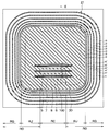
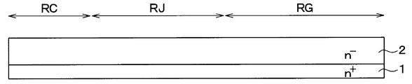
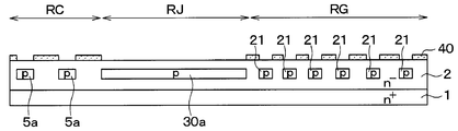
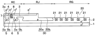
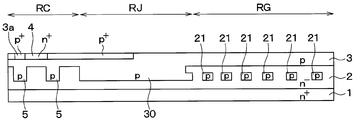
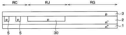
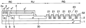
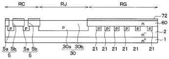
- the SiC semiconductor device shown in FIG. 1 is configured to have a cell region RC in which a trench gate type MOSFET 100 is formed, and an outer peripheral region RO surrounding the cell region RC.
- the outer peripheral region RO is configured to have a guard ring portion RG and a joint portion RJ disposed inside the guard ring portion RG, that is, between the cell region RC and the guard ring portion RG.
- FIG. 1 is not a cross-sectional view, hatching is partially shown for the sake of clarity.
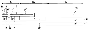
- the SiC semiconductor device is formed using an n + -type substrate 1 made of SiC.
- n + type substrate 1 made of SiC
- n ⁇ type layer 2 made of SiC and p type base region 3 are formed by epitaxial growth or the like, and further, n + type layer 2 is formed on the surface portion of p type base region 3.
- Source region 4 is formed.
- the n + -type substrate 1 has, for example, an n-type impurity concentration of 1.0 ⁇ 10 19 / cm 3 , a surface of (0001) Si, and an off direction of ⁇ 11-20>.
- the n -- type layer 2 has, for example, an n-type impurity concentration of 5.0 ⁇ 10 15 to 2.0 ⁇ 10 16 / cm 3 .
- the n -- type layer 2 constitutes an n-type layer serving as a drift layer.
- the p-type base region 3 has a p-type impurity concentration of, for example, about 2.0 ⁇ 10 17 / cm 3 and a thickness of 300 nm in the portion where the channel region is formed.
- a p-type contact region 3 a partially having a high concentration of p-type impurities is formed in the surface layer portion of the p-type base region 3, that is, in a place sandwiched by the n + -type source region 4.
- the n + -type source region 4 has an impurity concentration higher than that of the n ⁇ -type layer 2, and the n-type impurity concentration in the surface layer is, for example, 2.5 ⁇ 10 18 to 1.0 ⁇ 10 19 / cm 3 and thickness 0 .5 ⁇ m or so.
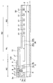
- p type base region 3 and n + type source region 4 are left on the surface side of n + type substrate 1, and in guard ring portion RG, p type base region 3 is penetrated to form n ⁇ type.
- a recess 20 is formed to reach layer 2.
- the p-type deep layer 5 corresponding to the first deep layer whose p-type impurity concentration is higher than that of the p-type base region 3 is formed in the surface layer of the n ⁇ -type layer 2. More specifically, the p-type deep layer 5 is formed from the position of a predetermined depth of the n ⁇ -type layer 2 to the surface, and for example, ion implantation of p-type impurities into the n ⁇ -type layer 2 It is formed of
- a plurality of p-type deep layers 5 are arranged in the n ⁇ -type layer 2 at equal intervals, and are arranged in a stripe shape by being arranged apart from each other without intersection.
- the p-type base region 3 and the n + -type source region 4 described above are formed on the p-type deep layer 5.
- Each p-type deep layer 5 is formed with the same impurity concentration, the same width, and the same depth, and, for example, the p-type impurity concentration is 1.0 ⁇ 10 17 to 1.0 ⁇ 10 19 / cm 3 , The width is about 0.7 ⁇ m and the depth is about 2.0 ⁇ m.
- Each p-type deep layer 5 is formed to extend from one end to the other end of the cell region RC as shown in FIG. Further, in the present embodiment, the p-type deep layer 5 is extended with the same direction as the trench gate structure to be described later as the longitudinal direction, and a connecting portion described later extended to the outside of the cell region RC at both ends of the trench gate structure. It is connected to the p-type deep layer 30 of RJ.
- the extending direction of the p-type deep layer 5 is arbitrary, but in the present embodiment, it is the same ⁇ 11-20> direction as the off direction.
- the width is 0.8 ⁇ m and the depth is so as to penetrate the p-type base region 3 and the n + -type source region 4 to reach the n ⁇ -type layer 2 and be shallower than the p-type deep layer 5.
- a gate trench 6 of 1.0 ⁇ m is formed.
- the p-type base region 3 and the n + -type source region 4 described above are arranged in contact with the side surfaces of the gate trench 6.
- the gate trench 6 is formed in a linear layout in which the lateral direction in the drawing of FIG. 2 is the width direction, the vertical direction in the drawing is the longitudinal direction, and the vertical direction in the drawing is the depth direction. Further, as shown in FIG. 1, the gate trenches 6 are arranged in a plurality such that they are respectively sandwiched between the p-type deep layers 5 and arranged in parallel at equal intervals to form a stripe shape. .
- the portion of p-type base region 3 located on the side surface of gate trench 6 functions as a channel region connecting n + -type source region 4 and n ⁇ -type layer 2 when vertical MOSFET 100 operates.
- a gate insulating film 7 is formed on the inner wall surface of the gate trench 6 including the channel region.
- a gate electrode 8 made of doped poly-Si is formed on the surface of the gate insulating film 7, and the inside of the gate trench 6 is completely filled with the gate insulating film 7 and the gate electrode 8.
- a trench gate structure is configured.
- FIG. 1 the trench gate structure and the number of the p-type deep layers 5 are illustrated with a reduced number for the sake of clarity. However, many similar structures are actually arranged.
- an interlayer insulating film 10 is formed on the opposite side of the n + -type substrate 1 across the n ⁇ -type layer 2, specifically, on the surfaces of the n + -type source region 4 and the p-type deep layer 5 and the gate electrode 8.
- a source electrode 9 corresponding to the first electrode, a gate wiring layer (not shown) and the like are formed via the The source electrode 9 and the gate wiring layer are made of a plurality of metals such as Ni / Al. Then, at least a portion of the plurality of metals in contact with the n-type SiC, specifically the n + -type source region 4 is made of a metal that can make an ohmic contact with the n-type SiC.
- At least a portion of the plurality of metals in contact with the p-type SiC, specifically the p-type contact region 3a, is made of a metal capable of being in ohmic contact with the p-type SiC.
- the source electrode 9 and the gate wiring layer are electrically isolated by being separated on the interlayer insulating film 10. Then, source electrode 9 is electrically connected to n + type source region 4 and p type contact region 3 a through the contact hole formed in interlayer insulating film 10, and the gate wiring layer is electrically connected to gate electrode 8. It is done.
- an n-channel type inverted trench gate structure MOSFET 100 is configured.
- a cell region RC is configured by arranging a plurality of such MOSFETs 100 in a plurality of cells.
- the recess 20 is formed to penetrate the p-type base region 3 and reach the n ⁇ -type layer 2. Therefore, the n + -type source region 4 and the p-type base region 3 are removed at positions away from the cell region RC, and the n ⁇ -type layer 2 is exposed. Then, in the thickness direction of the n + -type substrate 1, a cell region RC located inside the recess 20 and a part of the connecting portion RJ form a mesa portion protruding in an island shape.
- a plurality of p-type guard rings 21 are provided in the surface layer portion of the n ⁇ -type layer 2 located below the recess 20 so as to surround the cell region RC and the connecting portion RJ.
- the p-type guard ring 21 has a quadrangular shape in which the four corners are rounded, but may have another frame shape such as a circular shape.
- the p-type guard ring 21 is formed to a predetermined depth from a position distant from the surface of the n ⁇ -type layer 2, and is formed, for example, by ion implantation of a p-type impurity to the n ⁇ -type layer 2. It is done.
- the p-type guard ring 21 has the lower surface the same depth as the lower surface of the p-type deep layer 5, but unlike the p-type deep layer 5, the surface of the n ⁇ -type layer 2 is formed Since the upper surface is not located at a position deeper than the upper surface of the p-type deep layer 5.
- the p-type guard ring 21 has the same configuration as the above-described p-type deep layer 5 except that the depth is different.
- the p-type guard ring 21 is different from the p-type deep layer 5 formed in a straight line in that the upper surface shape is a frame-like line shape surrounding the cell region RC and the joint portion RJ, It is similar. That is, the p-type guard ring 21 has the same impurity concentration and the same width as the p-type deep layer 5. The intervals between the p-type guard rings 21 may be equal.
- the distance between the p-type guard rings 21 is narrow on the cell region RC side and on the outer side, so that the electric field concentration is alleviated on the inner side, that is, the cell region RC side and the equipotential lines are on the outer side. It is made so big.
- the guard ring portion RG including the outer peripheral withstand voltage structure surrounding the cell region RC is configured by providing the EQR structure on the outer periphery than the p-type guard ring 21 as necessary. .
- a p-type deep layer 30 corresponding to the second deep layer is formed in the surface layer portion of the n ⁇ -type layer 2 in the joint portion RJ, with the distance from the cell region RC to the guard ring portion RG as the joint portion RJ. ing.
- the p-type deep layer 30 is fixed to the source potential because it is in contact with the p-type base region 3.
- the connecting portion RJ is formed to surround the cell region RC, and the four corners are rounded so as to surround the outside of the connecting portion RJ.
- a plurality of square p-type guard rings 21 are formed.
- the p-type deep layer 30 is formed in a solid-line hatched portion which is the connecting portion RJ, and is connected to the p-type deep layer 5 formed in the cell region RC.
- Each p-type deep layer 30 is formed, for example, by ion-implanting a p-type impurity into the surface of the n ⁇ -type layer 2.
- the impurity concentration and depth of the p-type deep layer 30 are the same as those of the p-type deep layer 5 described above.
- the interlayer insulating film 10 is formed on the surface of the n + -type source region 4.
- the junction region RJ is formed between the cell region RC and the guard ring portion RG, and the p-type deep layer 30 is formed in the junction portion RJ, thereby p being disposed on both sides of the trench gate structure. And the deep layer 5 are connected.
- the equipotential lines are extended from the cell area RC toward the guard ring portion RG so as to be terminated at the guard ring portion RG while suppressing an excessive rise of the equipotential lines in the cell region RC. be able to.
- the SiC semiconductor device concerning this embodiment is constituted by the above structures.
- the SiC semiconductor device thus configured forms a channel region on the surface portion of p-type base region 3 located on the side surface of gate trench 6 by controlling the voltage applied to gate electrode 8 when MOSFET 100 is turned on. Do. Thereby, current flows between the source electrode 9 and the drain electrode 11 through the n + -type source region 4 and the n ⁇ -type layer 2.
- p-type deep layer 5 and p-type deep layer 30 formed to a position deeper than the trench gate structure suppress entry of an electric field to the bottom of the gate trench. Ru. Therefore, the electric field concentration at the bottom of the gate trench is alleviated. Thereby, the destruction of the gate insulating film 7 is prevented.
- the connecting portion RJ the rising of the equipotential line is suppressed, and the connection toward the guard ring portion RG is made. Further, in the guard ring portion RG, the equipotential line is gradually terminated toward the outer peripheral direction by the p-type guard ring 21, and a desired withstand voltage can be obtained even in the guard ring portion RG.
- each p-type guard ring 21 is formed at a position separated from the surface of n - type layer 2, so p-type guard ring 21 and n - type layer
- the boundary portion of the PN junction of 2 and 3 is separated from the interlayer insulating film 10. Therefore, even if electric field concentration occurs in the PN junction, the interlayer insulating film 10 is not in contact with the PN junction, so that the electric field strength applied to the interlayer insulating film 10 can be suppressed.
- the interlayer insulating film 10 and a protective film are further formed thereon, an increase in electric field strength on the outermost surface thereof can be suppressed, and the occurrence of creeping damage can be suppressed.
- the electric field strength at the outermost surface may be further increased by using a high voltage, but it is possible to suppress the occurrence of creeping fracture even when using SiC. Become.
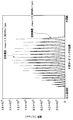
- FIG. 3 shows the result.
- simulation is performed about the case where 18 p-type guard rings 21 are formed here.
- the electric field strength at the boundary position with the n ⁇ -type layer 2 on the outer peripheral side of each p-type guard ring 21 Becomes larger.
- the maximum electric field strength is 0.98 MV / cm, which is a sufficiently smaller value than the conventional structure. From this, it is understood that the electric field strength at the interface between the interlayer insulating film 10 and SiC can be suppressed by adopting the structure of the present embodiment.
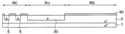
- a substrate obtained by epitaxially growing an n -- type layer 2 made of SiC on the main surface of an n + -type substrate 1 is prepared.
- the n + -type n on the main surface of the substrate 1 - to type layer 2 may be a semiconductor substrate by epitaxial growth
- n on the main surface of the pre-n + -type substrate 1 - -type layer 2 is A so-called epitaxial substrate epitaxially grown may be prepared as a semiconductor substrate.
- the mask 40 is disposed on the n ⁇ -type layer 2, and the mask 40 is opened in a region where the p-type deep layer 5, the p-type deep layer 30 and the p-type guard ring 21 are to be formed. Then, p-type impurities are ion-implanted using the mask 40. At this time, the range of ion implantation is adjusted so that the p-type impurity is implanted at a position deeper than the surface of the n ⁇ -type layer 2 by a predetermined depth, and the surface of the n ⁇ -type layer 2 is p-type impurity. It is almost impossible to inject it. Thus, the lower portion 5 a of the p-type deep layer 5 and the lower portion 30 a of the p-type deep layer 30 and the p-type guard ring 21 are formed. Thereafter, the mask 40 is removed.
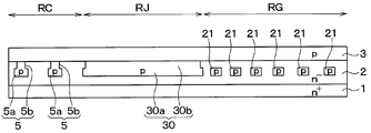
- the mask 41 is disposed, and the mask 41 is opened in a region where the p-type deep layer 5 and the p-type deep layer 30 are to be formed. At this time, the mask 41 is not opened in a region where the p-type guard ring 21 is to be formed. Then, p-type impurities are ion-implanted using the mask 41.
- the upper portion 5b of the p-type deep layer 5 and the upper portion 30b of the p-type deep layer 30 are formed, and are connected to the lower portion 5a of the p-type deep layer 5 formed previously and the lower portion 30a of the p-type deep layer 30
- the p-type deep layer 5 and the p-type deep layer 30 are configured. Thereafter, the mask 41 is removed.
- the widths of the upper portions 5b and 30b and the lower portions 5a and 30a of the p-type deep layer 5 and the p-type deep layer 30 may be the same, but may be different. In the case of this embodiment, the upper portions 5b and 30b of the p-type deep layer 5 and the p-type deep layer 30 are set to be narrower than the lower portions 5a and 30a. Also, the order of the process shown in FIG. 4B and the process shown in FIG. 4C may be switched, and the process shown in FIG. 4C may be performed before the process shown in FIG. 4B.
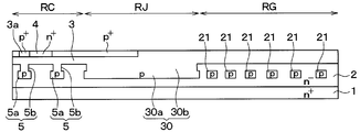
- the p-type base region 3 is epitaxially grown on the n ⁇ -type layer 2 including the p-type deep layer 5, the p-type deep layer 30 and the p-type guard ring 21.
- Step shown in FIG. 4E After arranging a mask (not shown) on the p-type base region 3, an area scheduled to form the n + -type source region 4 in the mask is opened. Then, an n + -type source region 4 is formed by ion-implanting an n-type impurity using the mask. Furthermore, after removing the mask, a mask (not shown) is arranged again, and an area for forming the p-type contact region 3a of the mask is opened. Then, p-type contact regions 3a are formed by ion-implanting p-type impurities using the mask. After that, the mask is removed.
- n + -type source region 4 and the p-type contact region 3a are formed by ion implantation here, one of them may be formed by epitaxial growth and the other may be formed by ion implantation.
- Step shown in FIG. 4F After a mask (not shown) is formed on the n + -type source region 4 and the p-type base region 3 and the like, regions for forming the gate trench 6 and the recess 20 in the mask are opened. Then, by performing anisotropic etching such as RIE (Reactive Ion Etching) using a mask, gate trenches 6 deeper than the upper surface of the n ⁇ type layer 2 and shallower than the upper surface of the p type guard ring 21. And the recess 20 are formed simultaneously.
- anisotropic etching such as RIE (Reactive Ion Etching)
- the gate trench 6 and the recess 20 are formed simultaneously here, they can be formed separately. In that case, since the gate trench 6 and the recess 20 can be made to have different depths, it is also possible to design each to an optimal depth.
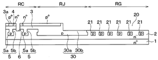
- the gate insulating film 7 is formed, for example, by thermal oxidation, and the gate insulating film 7 covers the inner wall surface of the gate trench 6 and the surface of the n + -type source region 4. Then, after depositing Poly-Si doped with p-type impurities or n-type impurities, this is etched back to leave at least Poly-Si in the gate trench 6 to form the gate electrode 8. This forms a trench gate structure.
- An interlayer insulating film 10 made of, for example, an oxide film or the like is formed to cover the surfaces of the gate electrode 8 and the gate insulating film 7. Then, after forming a mask (not shown) on the surface of interlayer insulating film 10, a portion of the mask located between gate electrodes 8, that is, a portion corresponding to p-type contact region 3a and the vicinity thereof are opened. Thereafter, the interlayer insulating film 10 is patterned using a mask to form a contact hole for exposing the p-type contact region 3 a and the n + -type source region 4.
- Step shown in FIG. 4I On the surface of the interlayer insulating film 10, an electrode material composed of, for example, a laminated structure of a plurality of metals is formed. Then, the electrode material is patterned to form a source electrode 9 and a gate wiring (not shown).
- the process of forming the drain electrode 11 on the back surface side of the n + -type substrate 1 is performed to complete the SiC semiconductor device according to the present embodiment.
- each p-type guard ring 21 the n - has to be formed at a position away from the mold layer 2 of the surface, the p-type guard ring 21 and the n -
- the boundary portion of the PN junction with the mold layer 2 is in a state of being separated from the interlayer insulating film 10. Therefore, even if electric field concentration occurs in the PN junction, the interlayer insulating film 10 is not in contact with the PN junction, so that the electric field strength applied to the interlayer insulating film 10 can be suppressed. Therefore, when the interlayer insulating film 10 and a protective film (not shown) are further formed thereon, an increase in electric field strength on the outermost surface thereof can be suppressed, and the occurrence of creeping damage can be suppressed.
- the second embodiment will be described.
- the present embodiment is the same as the first embodiment except that the manufacturing method is changed with respect to the first embodiment, and therefore parts different from the first embodiment will be mainly described.
- the method of manufacturing the SiC semiconductor device according to the present embodiment will be described with reference to the method of manufacturing the SiC semiconductor device according to the first embodiment described above.
- a semiconductor substrate is prepared in which the n ⁇ -type layer 2 made of SiC is epitaxially grown on the main surface of the n + -type substrate 1. Then, the processes shown in FIGS. 5A to 5D are performed.
- a mask 50 is disposed on the n ⁇ -type layer 2, and the mask 50 is opened in a region where the p-type deep layer 5 and the p-type deep layer 30 are to be formed. Then, p-type impurities are ion-implanted using the mask 50. Thereby, the p-type deep layer 5 and the p-type deep layer 30 are formed. Thereafter, the mask 50 is removed.
- Step shown in FIG. 5B Next, as a step shown in FIG. 5B, the mask 51 is disposed on the n ⁇ -type layer 2 and the mask 51 is opened in a region where the p-type deep layer 30 and the p-type guard ring 21 are to be formed. Then, p-type impurities are ion-implanted using the mask 51. At this time, the range of ion implantation is adjusted so that the p-type impurity is implanted at a position deeper than the surface of the n ⁇ -type layer 2 by a predetermined depth, and the surface of the n ⁇ -type layer 2 is p-type impurity. It is almost impossible to inject it. Thus, the p-type guard ring 21 can be formed, and the portion of the p-type deep layer 30 on the p-type guard ring 21 side can be formed. Thereafter, the mask 51 is removed.
- the p-type guard ring 21 is formed, but also the portion of the p-type deep layer 30 on the p-type guard ring 21 side is formed. This is because when the p-type deep layer 30 is formed only by the process shown in FIG. 5A, the distance between the p-type deep layer 30 and the p-type guard ring 21 may vary depending on the mask alignment accuracy. Thus, by simultaneously forming the end of the p-type deep layer 30 on the p-type guard ring 21 side when forming the p-type guard ring 21, the p-type deep layer 30 and the p-type guard ring 21 and It is possible to eliminate the variation of the interval of
- steps shown in FIG. 5C and FIG. 5D steps shown in FIG. 4D and FIG. 4E described in the first embodiment are performed.
- steps shown in FIG. 4F described in the first embodiment are performed.
- n - step of forming the p-type deep layer 5 and the p-type deep layer 30 is formed to the surface of the mold layer 2, n - p-type guard ring not only formed up to a position away from the surface of the mold layer 2 It may be performed separately from the forming process of 21. Also in this case, the SiC semiconductor device having the structure shown in the first embodiment can be manufactured.
- the end of the p-type deep layer 30 on the p-type guard ring 21 side is also formed simultaneously with the formation of the p-type guard ring 21, whereby the distance between the p-type deep layer 30 and the p-type guard ring 21. Can be eliminated.
- the p-type guard ring 21 is formed in the process shown in FIG. 5B. You should do it.
- Third Embodiment A third embodiment will be described. This embodiment is also a modification of the manufacturing method of the first embodiment, and the other parts are the same as the first embodiment, and therefore, parts different from the first embodiment will be mainly described.
- the method of manufacturing the SiC semiconductor device according to the present embodiment will be described with reference to the method of manufacturing the SiC semiconductor device according to the first embodiment described above.
- a semiconductor substrate is prepared in which the n ⁇ -type layer 2 made of SiC is epitaxially grown on the main surface of the n + -type substrate 1. Also, the p-type deep layer 5 and the p-type deep layer 30 are formed by performing the same steps as the steps shown in FIG. 5A described in the second embodiment. Then, the processes shown in FIGS. 6A to 6D are performed.
- the p-type base region 3 is formed by performing the same step as FIG. 4D without forming the p-type guard ring 21. Then, in the step shown in FIG. 6B, the n + -type source region 4 and the p-type contact region 3a are formed by performing the same step as the step shown in FIG. 4E. Further, as the step shown in FIG. 6C, the gate trench 6 and the recess 20 are formed by performing the same step as the step shown in FIG. 4F.
- the mask 52 is disposed on the n ⁇ -type layer 2 and the mask 52 is opened in a region where the p-type deep layer 30 and the p-type guard ring 21 are to be formed.
- p-type impurities are ion-implanted into the bottom of the recess 20 using the mask 52.
- the range of ion implantation is adjusted so that the p-type impurity is implanted at a predetermined depth deeper than the surface of the n ⁇ -type layer 2 in the recess 20, and the surface of the n ⁇ -type layer 2 is The p-type impurity is not substantially implanted.
- the p-type guard ring 21 can be formed, and a portion of the p-type deep layer 30 on the p-type guard ring 21 side can be formed.
- the mask 52 is removed.
- the variation in the distance between the p-type deep layer 30 and the p-type guard ring 21 can be eliminated.
- the variation in the distance between the p-type deep layer 30 and the p-type guard ring 21 may be within the allowable range, and in that case, in the process shown in FIG. Only the mold guard ring 21 may be formed.
- the concave portion 20 n - perform p-type deep layer 5 and the p-type deep layer 30 of the forming step is formed to the surface of the mold layer 2, n after the formation of the recess 20 - the surface of the mold layer 2
- the step of forming the p-type guard ring 21 may be performed only to a position away from the p-type. Also in this case, the SiC semiconductor device having the structure shown in the first embodiment can be manufactured.
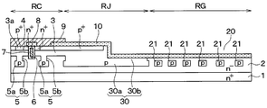
- the present embodiment is configured to include a current distribution layer with respect to the first embodiment, and the other parts are the same as the first embodiment, and therefore, only different parts from the first embodiment will be described.
- an n-type current dispersion layer 60 is provided, and a p-type base region 3 is formed on the n ⁇ -type layer 2 via the current dispersion layer 60.
- the structure is formed. That is, in the case of the present embodiment, at a position of depth corresponding to the upper portion 5 b of the p-type deep layer 5 and the upper portion 30 b of the p-type deep layer 30, a portion which is not made the p-type deep layer 5 or the p-type deep layer 30 Is the current distribution layer 60.
- the current distribution layer 60 is also formed between the p-type guard ring 21 and the interlayer insulating film 10.
- the current dispersion layer 60 has an n-type impurity concentration of 2.0 ⁇ 10 16 to 5.0 ⁇ 10 17 / cm 3 and a thickness of 0.5 to 0.9 ⁇ m.
- the thickness is 0.2 to 0.6 ⁇ m because a part of the outer peripheral region RO is removed when the concave portion 20 is formed as described later.
- the current dispersion layer 60 is a layer in which the n-type impurity concentration is higher than that of the n ⁇ -type layer 2, that is, the resistance is low.
- the current can be dispersed in a wider range in the current distribution layer 60, and the JFET resistance can be reduced.
- the p-type base region 3 can be formed on the n -- type layer 2 with the current distribution layer 60 interposed therebetween.
- n - will be -type layer 2 and the current spreading layer 60 constituting the n-type layer serving as a drift layer, n - -type layer 2 is first The layers are formed, and the current distribution layer 60 forms the second layer.
- ion implantation is performed on the current dispersion layer 60 to form the upper portions 5b and 30b of the p-type deep layer 5 and the p-type deep layer 30.
- ion-implant also into a portion of the current dispersion layer 60 corresponding to the p-type guard ring 21.
- the p-type guard ring 21 is in contact with the interlayer insulating film 10, which may cause the occurrence of creeping failure. Further, as shown in FIG.
- the process of forming the lower portion 21 a formed on the surface portion of the n ⁇ -type layer 2 and the upper portion 21 b formed on the current dispersion layer 60 are separate steps. It becomes. For this reason, a shift may occur in the formation position of the upper portion 21 b and the lower portion 21 a due to the mask shift in forming each of them. As a result, the distance between the adjacent p-type guard rings 21 becomes narrow, and if the amount of displacement is large, the electric field relaxation function of the p-type guard ring 21 can not be exhibited and the withstand voltage in the outer peripheral region RO can not be obtained. generate.
- the p-type guard ring 21 is formed only on the surface layer portion of the n ⁇ -type layer 2 and not formed on the current dispersion layer 60 as in the present embodiment, the problem of mask displacement can not occur. Therefore, the distance between adjacent p-type guard rings 21 can be set to a desired value, and the p-type guard ring 21 can exhibit the electric field relaxation effect, and the withstand voltage in the outer peripheral region RO can be secured. become.
- the p-type guard ring 21 shown in FIG. 8 is also formed on the current dispersion layer 60, the amount of displacement between the lower portion 21a and the upper portion 21b due to mask displacement As the breakdown voltage changes and the amount of deviation increases, the breakdown voltage drops significantly.
- the p-type guard ring 21 is separated from the interlayer insulating film 10 by not forming the p-type guard ring 21 in the current distribution layer 60 as in the present embodiment, it is assumed that a mask displacement occurs. Also, almost no drop in withstand voltage occurred. Thus, with the structure of the present embodiment, it is possible to secure the withstand voltage in the outer peripheral region RO.
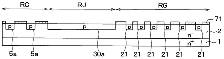
- a semiconductor substrate is prepared in which the n ⁇ -type layer 2 made of SiC is epitaxially grown on the main surface of the n + -type substrate 1. Then, the processes shown in FIGS. 10A to 10C are performed.
- a mask 71 is disposed on the n ⁇ -type layer 2, and the mask 71 is opened in a region where the p-type deep layer 5, the p-type deep layer 30 and the p-type guard ring 21 are to be formed. Then, p-type impurities are ion-implanted using the mask 71. As a result, the lower portion 5a of the p-type deep layer 5 and the lower portion 30a of the p-type deep layer 30 are formed from the surface of the n -- type layer 2 to a predetermined depth, and the p-type guard ring 21 is formed. Thereafter, the mask 71 is removed.
- the n-type impurity concentration is 2.0 ⁇ 10 16 to 5.0.
- An n-type current dispersion layer 60 having a thickness of 0.5 to 0.9 ⁇ m is epitaxially grown on 10 17 / cm 3 .
- a mask 72 is disposed on the current spreading layer 60, and the mask 72 is opened in a region where the p-type deep layer 5 and the p-type deep layer 30 are to be formed. Then, p-type impurities are ion-implanted using the mask 72. Thereby, the p-type deep layer 5 and the p-type deep layer 30 are formed. Thereafter, the mask 72 is removed.
- the steps shown in FIGS. 4C to 4E described in the first embodiment are performed.
- the p-type base region 3, the n + -type source region 4 and the p-type contact region 3 a are formed, and the gate trench 6 and the recess 20 are formed.
- the surface layer portion of the current dispersion layer 60 is etched by about 0.3 ⁇ m so as to penetrate the p-type base region 3 and reach the current distribution layer 60. Therefore, the thickness of the current dispersion layer 60 is 0.2 to 0.6 ⁇ m in the recess 20 and in the lower part of the gate trench 6.
- the etching amount is adjusted so that the current dispersion layer 60 is not removed too much and disappears.
- SiC semiconductor device concerning this embodiment can be manufactured by performing a process after a process shown in Drawing 4F explained by a 1st embodiment also after this.
- the MOSFET 100 is taken as an example of the semiconductor element provided in the cell region RC of the SiC semiconductor device.
- the p-type guard ring 21 in the outer peripheral region RO may not be in contact with the interlayer insulating film 10.
- a Schottky diode, IGBT, etc. can be mentioned, for example.
- the n-channel type MOSFET 100 in which the first conductivity type is n-type and the second conductivity type is p-type is described as an example, but p is the conductivity type of each component inverted.
- a channel type MOSFET 100 may be used.
- the IGBT only changes the conductivity type of the n + -type substrate 1 from the n-type to the p-type in each of the above embodiments, and the other structure and manufacturing method are the same as in each of the above embodiments.
- the distance between the p-type guard rings 21 may be constant, or the width of each p-type guard ring 21 may be wider toward the outer periphery. .
- the method of forming the p-type deep layer 5, the p-type deep layer 30, and the p-type guard ring 21 is not limited to ion implantation, and may be another forming method, for example, epitaxial growth.
- the p-type deep layer 5 and the lower portions 5 a and 30 a of the p-type deep layer 30 and the p-type guard ring 21 are formed from the surface of the n ⁇ -type layer 2 to a position of a predetermined depth. However, it may be formed only to a position away from the surface of the n ⁇ -type layer 2. In that case, in the process shown in FIG. 10C, p-type impurities are also implanted into the surface layer portion of the n ⁇ -type layer 2 when forming the upper portions 5 b and 30 b of the p-type deep layer 5 and p-type deep layer 30. Do. Then, upper portions 5 b and 30 b of the p-type deep layer 5 and the p-type deep layer 30 may be connected to lower portions 5 a and 30 a.
- a bar (-) should normally be added above the desired number, but since there is a limitation in expression based on the electronic application, it is desirable in the present specification to be a desired one. A bar shall be put in front of the numbers.
Landscapes
- Physics & Mathematics (AREA)
- High Energy & Nuclear Physics (AREA)
- Engineering & Computer Science (AREA)
- Health & Medical Sciences (AREA)
- Toxicology (AREA)
- Condensed Matter Physics & Semiconductors (AREA)
- General Physics & Mathematics (AREA)
- Manufacturing & Machinery (AREA)
- Computer Hardware Design (AREA)
- Microelectronics & Electronic Packaging (AREA)
- Power Engineering (AREA)
- Electrodes Of Semiconductors (AREA)
Priority Applications (2)
| Application Number | Priority Date | Filing Date | Title |
|---|---|---|---|
| CN201880058819.XA CN111344866B (zh) | 2017-09-14 | 2018-09-13 | 半导体装置及其制造方法 |
| US16/816,463 US10964809B2 (en) | 2017-09-14 | 2020-03-12 | Semiconductor device and manufacturing process therefor |
Applications Claiming Priority (2)
| Application Number | Priority Date | Filing Date | Title |
|---|---|---|---|
| JP2017176776A JP6870546B2 (ja) | 2017-09-14 | 2017-09-14 | 半導体装置およびその製造方法 |
| JP2017-176776 | 2017-09-14 |
Related Child Applications (1)
| Application Number | Title | Priority Date | Filing Date |
|---|---|---|---|
| US16/816,463 Continuation US10964809B2 (en) | 2017-09-14 | 2020-03-12 | Semiconductor device and manufacturing process therefor |
Publications (1)
| Publication Number | Publication Date |
|---|---|
| WO2019054459A1 true WO2019054459A1 (ja) | 2019-03-21 |
Family
ID=65722758
Family Applications (1)
| Application Number | Title | Priority Date | Filing Date |
|---|---|---|---|
| PCT/JP2018/034065 Ceased WO2019054459A1 (ja) | 2017-09-14 | 2018-09-13 | 半導体装置およびその製造方法 |
Country Status (4)
| Country | Link |
|---|---|
| US (1) | US10964809B2 (enExample) |
| JP (1) | JP6870546B2 (enExample) |
| CN (1) | CN111344866B (enExample) |
| WO (1) | WO2019054459A1 (enExample) |
Families Citing this family (18)
| Publication number | Priority date | Publication date | Assignee | Title |
|---|---|---|---|---|
| US11450734B2 (en) | 2019-06-17 | 2022-09-20 | Fuji Electric Co., Ltd. | Semiconductor device and fabrication method for semiconductor device |
| CN112349771A (zh) * | 2020-09-30 | 2021-02-09 | 湖南大学 | 一种碳化硅器件埋层型终端结构及其制备方法 |
| EP4240722A1 (en) * | 2020-11-06 | 2023-09-13 | Aligos Therapeutics, Inc. | Oxindoles and methods of use thereof |
| JP7647104B2 (ja) | 2021-01-06 | 2025-03-18 | 富士電機株式会社 | 半導体装置 |
| JP7647239B2 (ja) | 2021-03-30 | 2025-03-18 | 富士電機株式会社 | 半導体装置 |
| JP7687035B2 (ja) * | 2021-04-23 | 2025-06-03 | 富士電機株式会社 | 半導体装置 |
| JP7697255B2 (ja) | 2021-04-27 | 2025-06-24 | 富士電機株式会社 | 炭化珪素半導体装置および炭化珪素半導体装置の製造方法 |
| JP7647452B2 (ja) * | 2021-08-31 | 2025-03-18 | 株式会社デンソー | 半導体装置およびその製造方法 |
| JP2023056697A (ja) * | 2021-10-08 | 2023-04-20 | 株式会社デンソー | 半導体装置およびその製造方法 |
| JP2023088816A (ja) * | 2021-12-15 | 2023-06-27 | 富士電機株式会社 | 炭化珪素半導体装置 |
| CN114335141A (zh) * | 2021-12-20 | 2022-04-12 | 深圳基本半导体有限公司 | 一种复合场限环终端结构及制备方法 |
| JP2023102946A (ja) * | 2022-01-13 | 2023-07-26 | 富士電機株式会社 | 炭化珪素半導体装置 |
| CN115498013B (zh) * | 2022-07-21 | 2024-04-26 | 上海林众电子科技有限公司 | 一种功率芯片终结区的制备方法、终结区的结构及功率芯片 |
| CN115472495B (zh) * | 2022-07-21 | 2024-05-31 | 上海林众电子科技有限公司 | 一种功率芯片终结区的制备方法及功率芯片的制备方法 |
| CN115020240B (zh) * | 2022-08-03 | 2023-03-28 | 上海维安半导体有限公司 | 一种低压超结沟槽mos器件的制备方法及结构 |
| JP2024060452A (ja) * | 2022-10-19 | 2024-05-02 | 株式会社デンソー | 半導体装置とその製造方法 |
| WO2025028616A1 (ja) * | 2023-08-03 | 2025-02-06 | ローム株式会社 | 半導体装置 |
| CN117790537B (zh) * | 2023-12-28 | 2024-10-25 | 深圳平湖实验室 | 一种半导体器件、其制作方法及电子器件 |
Citations (6)
| Publication number | Priority date | Publication date | Assignee | Title |
|---|---|---|---|---|
| JP2008004643A (ja) * | 2006-06-20 | 2008-01-10 | Toshiba Corp | 半導体装置 |
| JP2014170778A (ja) * | 2013-03-01 | 2014-09-18 | Sumitomo Electric Ind Ltd | 炭化珪素半導体装置 |
| JP2015076592A (ja) * | 2013-10-11 | 2015-04-20 | 住友電気工業株式会社 | 炭化珪素半導体装置およびその製造方法 |
| JP2015153787A (ja) * | 2014-02-10 | 2015-08-24 | トヨタ自動車株式会社 | 半導体装置及び半導体装置の製造方法 |
| EP3012870A1 (en) * | 2014-10-20 | 2016-04-27 | ABB Technology AG | Edge termination for high voltage semiconductor devices |
| JP2016066780A (ja) * | 2014-09-16 | 2016-04-28 | 株式会社デンソー | 炭化珪素半導体装置およびその製造方法 |
Family Cites Families (8)
| Publication number | Priority date | Publication date | Assignee | Title |
|---|---|---|---|---|
| JP2000022176A (ja) * | 1998-06-30 | 2000-01-21 | Toshiba Corp | 電力用半導体装置 |
| JP4450122B2 (ja) * | 1999-11-17 | 2010-04-14 | 株式会社デンソー | 炭化珪素半導体装置 |
| US7737469B2 (en) | 2006-05-16 | 2010-06-15 | Kabushiki Kaisha Toshiba | Semiconductor device having superjunction structure formed of p-type and n-type pillar regions |
| CN101872790A (zh) * | 2009-04-27 | 2010-10-27 | 得诣科技股份有限公司 | 具有外延式护环的肖特基二极管元件及其制作方法 |
| JP5224289B2 (ja) * | 2009-05-12 | 2013-07-03 | 三菱電機株式会社 | 半導体装置 |
| JP5812029B2 (ja) * | 2012-06-13 | 2015-11-11 | 株式会社デンソー | 炭化珪素半導体装置およびその製造方法 |
| JP6409681B2 (ja) * | 2015-05-29 | 2018-10-24 | 株式会社デンソー | 半導体装置およびその製造方法 |
| JP6740759B2 (ja) * | 2016-07-05 | 2020-08-19 | 株式会社デンソー | 炭化珪素半導体装置およびその製造方法 |
-
2017
- 2017-09-14 JP JP2017176776A patent/JP6870546B2/ja active Active
-
2018
- 2018-09-13 CN CN201880058819.XA patent/CN111344866B/zh active Active
- 2018-09-13 WO PCT/JP2018/034065 patent/WO2019054459A1/ja not_active Ceased
-
2020
- 2020-03-12 US US16/816,463 patent/US10964809B2/en active Active
Patent Citations (6)
| Publication number | Priority date | Publication date | Assignee | Title |
|---|---|---|---|---|
| JP2008004643A (ja) * | 2006-06-20 | 2008-01-10 | Toshiba Corp | 半導体装置 |
| JP2014170778A (ja) * | 2013-03-01 | 2014-09-18 | Sumitomo Electric Ind Ltd | 炭化珪素半導体装置 |
| JP2015076592A (ja) * | 2013-10-11 | 2015-04-20 | 住友電気工業株式会社 | 炭化珪素半導体装置およびその製造方法 |
| JP2015153787A (ja) * | 2014-02-10 | 2015-08-24 | トヨタ自動車株式会社 | 半導体装置及び半導体装置の製造方法 |
| JP2016066780A (ja) * | 2014-09-16 | 2016-04-28 | 株式会社デンソー | 炭化珪素半導体装置およびその製造方法 |
| EP3012870A1 (en) * | 2014-10-20 | 2016-04-27 | ABB Technology AG | Edge termination for high voltage semiconductor devices |
Also Published As
| Publication number | Publication date |
|---|---|
| US10964809B2 (en) | 2021-03-30 |
| CN111344866A (zh) | 2020-06-26 |
| CN111344866B (zh) | 2023-06-16 |
| US20200227549A1 (en) | 2020-07-16 |
| JP2019054087A (ja) | 2019-04-04 |
| JP6870546B2 (ja) | 2021-05-12 |
Similar Documents
| Publication | Publication Date | Title |
|---|---|---|
| WO2019054459A1 (ja) | 半導体装置およびその製造方法 | |
| US11769801B2 (en) | Silicon carbide semiconductor device with cell section and outer periphery section | |
| CN109417087B (zh) | 碳化硅半导体装置及其制造方法 | |
| JP6696328B2 (ja) | 炭化珪素半導体装置およびその製造方法 | |
| JP6696329B2 (ja) | 炭化珪素半導体装置およびその製造方法 | |
| US10784335B2 (en) | Silicon carbide semiconductor device and manufacturing method therefor | |
| JP7420485B2 (ja) | 炭化珪素半導体装置およびその製造方法 | |
| US10714611B2 (en) | Silicon carbide semiconductor device | |
| JP7647452B2 (ja) | 半導体装置およびその製造方法 |
Legal Events
| Date | Code | Title | Description |
|---|---|---|---|
| 121 | Ep: the epo has been informed by wipo that ep was designated in this application |
Ref document number: 18855638 Country of ref document: EP Kind code of ref document: A1 |
|
| NENP | Non-entry into the national phase |
Ref country code: DE |
|
| 122 | Ep: pct application non-entry in european phase |
Ref document number: 18855638 Country of ref document: EP Kind code of ref document: A1 |