WO2019049659A1 - 機能性チップを備える基板を研磨する方法 - Google Patents
機能性チップを備える基板を研磨する方法 Download PDFInfo
- Publication number
- WO2019049659A1 WO2019049659A1 PCT/JP2018/030894 JP2018030894W WO2019049659A1 WO 2019049659 A1 WO2019049659 A1 WO 2019049659A1 JP 2018030894 W JP2018030894 W JP 2018030894W WO 2019049659 A1 WO2019049659 A1 WO 2019049659A1
- Authority
- WO
- WIPO (PCT)
- Prior art keywords
- polishing
- substrate
- insulating material
- end point
- light
- Prior art date
- Legal status (The legal status is an assumption and is not a legal conclusion. Google has not performed a legal analysis and makes no representation as to the accuracy of the status listed.)
- Ceased
Links
Images






Classifications
-
- B—PERFORMING OPERATIONS; TRANSPORTING
- B24—GRINDING; POLISHING
- B24B—MACHINES, DEVICES, OR PROCESSES FOR GRINDING OR POLISHING; DRESSING OR CONDITIONING OF ABRADING SURFACES; FEEDING OF GRINDING, POLISHING, OR LAPPING AGENTS
- B24B37/00—Lapping machines or devices; Accessories
- B24B37/11—Lapping tools
- B24B37/12—Lapping plates for working plane surfaces
- B24B37/16—Lapping plates for working plane surfaces characterised by the shape of the lapping plate surface, e.g. grooved
-
- H—ELECTRICITY
- H10—SEMICONDUCTOR DEVICES; ELECTRIC SOLID-STATE DEVICES NOT OTHERWISE PROVIDED FOR
- H10P—GENERIC PROCESSES OR APPARATUS FOR THE MANUFACTURE OR TREATMENT OF DEVICES COVERED BY CLASS H10
- H10P52/00—Grinding, lapping or polishing of wafers, substrates or parts of devices
- H10P52/40—Chemomechanical polishing [CMP]
- H10P52/402—Chemomechanical polishing [CMP] of semiconductor materials
-
- B—PERFORMING OPERATIONS; TRANSPORTING
- B24—GRINDING; POLISHING
- B24B—MACHINES, DEVICES, OR PROCESSES FOR GRINDING OR POLISHING; DRESSING OR CONDITIONING OF ABRADING SURFACES; FEEDING OF GRINDING, POLISHING, OR LAPPING AGENTS
- B24B37/00—Lapping machines or devices; Accessories
- B24B37/005—Control means for lapping machines or devices
- B24B37/013—Devices or means for detecting lapping completion
-
- B—PERFORMING OPERATIONS; TRANSPORTING
- B24—GRINDING; POLISHING
- B24B—MACHINES, DEVICES, OR PROCESSES FOR GRINDING OR POLISHING; DRESSING OR CONDITIONING OF ABRADING SURFACES; FEEDING OF GRINDING, POLISHING, OR LAPPING AGENTS
- B24B49/00—Measuring or gauging equipment for controlling the feed movement of the grinding tool or work; Arrangements of indicating or measuring equipment, e.g. for indicating the start of the grinding operation
- B24B49/02—Measuring or gauging equipment for controlling the feed movement of the grinding tool or work; Arrangements of indicating or measuring equipment, e.g. for indicating the start of the grinding operation according to the instantaneous size and required size of the workpiece acted upon, the measuring or gauging being continuous or intermittent
- B24B49/04—Measuring or gauging equipment for controlling the feed movement of the grinding tool or work; Arrangements of indicating or measuring equipment, e.g. for indicating the start of the grinding operation according to the instantaneous size and required size of the workpiece acted upon, the measuring or gauging being continuous or intermittent involving measurement of the workpiece at the place of grinding during grinding operation
-
- B—PERFORMING OPERATIONS; TRANSPORTING
- B24—GRINDING; POLISHING
- B24B—MACHINES, DEVICES, OR PROCESSES FOR GRINDING OR POLISHING; DRESSING OR CONDITIONING OF ABRADING SURFACES; FEEDING OF GRINDING, POLISHING, OR LAPPING AGENTS
- B24B49/00—Measuring or gauging equipment for controlling the feed movement of the grinding tool or work; Arrangements of indicating or measuring equipment, e.g. for indicating the start of the grinding operation
- B24B49/10—Measuring or gauging equipment for controlling the feed movement of the grinding tool or work; Arrangements of indicating or measuring equipment, e.g. for indicating the start of the grinding operation involving electrical means
-
- B—PERFORMING OPERATIONS; TRANSPORTING
- B24—GRINDING; POLISHING
- B24B—MACHINES, DEVICES, OR PROCESSES FOR GRINDING OR POLISHING; DRESSING OR CONDITIONING OF ABRADING SURFACES; FEEDING OF GRINDING, POLISHING, OR LAPPING AGENTS
- B24B49/00—Measuring or gauging equipment for controlling the feed movement of the grinding tool or work; Arrangements of indicating or measuring equipment, e.g. for indicating the start of the grinding operation
- B24B49/12—Measuring or gauging equipment for controlling the feed movement of the grinding tool or work; Arrangements of indicating or measuring equipment, e.g. for indicating the start of the grinding operation involving optical means
-
- B—PERFORMING OPERATIONS; TRANSPORTING
- B24—GRINDING; POLISHING
- B24B—MACHINES, DEVICES, OR PROCESSES FOR GRINDING OR POLISHING; DRESSING OR CONDITIONING OF ABRADING SURFACES; FEEDING OF GRINDING, POLISHING, OR LAPPING AGENTS
- B24B49/00—Measuring or gauging equipment for controlling the feed movement of the grinding tool or work; Arrangements of indicating or measuring equipment, e.g. for indicating the start of the grinding operation
- B24B49/16—Measuring or gauging equipment for controlling the feed movement of the grinding tool or work; Arrangements of indicating or measuring equipment, e.g. for indicating the start of the grinding operation taking regard of the load
-
- H—ELECTRICITY
- H10—SEMICONDUCTOR DEVICES; ELECTRIC SOLID-STATE DEVICES NOT OTHERWISE PROVIDED FOR
- H10P—GENERIC PROCESSES OR APPARATUS FOR THE MANUFACTURE OR TREATMENT OF DEVICES COVERED BY CLASS H10
- H10P52/00—Grinding, lapping or polishing of wafers, substrates or parts of devices
-
- H—ELECTRICITY
- H10—SEMICONDUCTOR DEVICES; ELECTRIC SOLID-STATE DEVICES NOT OTHERWISE PROVIDED FOR
- H10P—GENERIC PROCESSES OR APPARATUS FOR THE MANUFACTURE OR TREATMENT OF DEVICES COVERED BY CLASS H10
- H10P74/00—Testing or measuring during manufacture or treatment of wafers, substrates or devices
- H10P74/23—Testing or measuring during manufacture or treatment of wafers, substrates or devices characterised by multiple measurements, corrections, marking or sorting processes
- H10P74/238—Testing or measuring during manufacture or treatment of wafers, substrates or devices characterised by multiple measurements, corrections, marking or sorting processes comprising acting in response to an ongoing measurement without interruption of processing, e.g. endpoint detection or in-situ thickness measurement
-
- H—ELECTRICITY
- H10—SEMICONDUCTOR DEVICES; ELECTRIC SOLID-STATE DEVICES NOT OTHERWISE PROVIDED FOR
- H10W—GENERIC PACKAGES, INTERCONNECTIONS, CONNECTORS OR OTHER CONSTRUCTIONAL DETAILS OF DEVICES COVERED BY CLASS H10
- H10W74/00—Encapsulations, e.g. protective coatings
- H10W74/01—Manufacture or treatment
- H10W74/012—Manufacture or treatment of encapsulations on active surfaces of flip-chip devices, e.g. forming underfills
-
- H—ELECTRICITY
- H10—SEMICONDUCTOR DEVICES; ELECTRIC SOLID-STATE DEVICES NOT OTHERWISE PROVIDED FOR
- H10W—GENERIC PACKAGES, INTERCONNECTIONS, CONNECTORS OR OTHER CONSTRUCTIONAL DETAILS OF DEVICES COVERED BY CLASS H10
- H10W74/00—Encapsulations, e.g. protective coatings
- H10W74/01—Manufacture or treatment
- H10W74/014—Manufacture or treatment using batch processing
-
- H—ELECTRICITY
- H10—SEMICONDUCTOR DEVICES; ELECTRIC SOLID-STATE DEVICES NOT OTHERWISE PROVIDED FOR
- H10W—GENERIC PACKAGES, INTERCONNECTIONS, CONNECTORS OR OTHER CONSTRUCTIONAL DETAILS OF DEVICES COVERED BY CLASS H10
- H10W74/00—Encapsulations, e.g. protective coatings
- H10W74/10—Encapsulations, e.g. protective coatings characterised by their shape or disposition
- H10W74/15—Encapsulations, e.g. protective coatings characterised by their shape or disposition on active surfaces of flip-chip devices, e.g. underfills
-
- H—ELECTRICITY
- H10—SEMICONDUCTOR DEVICES; ELECTRIC SOLID-STATE DEVICES NOT OTHERWISE PROVIDED FOR
- H10W—GENERIC PACKAGES, INTERCONNECTIONS, CONNECTORS OR OTHER CONSTRUCTIONAL DETAILS OF DEVICES COVERED BY CLASS H10
- H10W70/00—Package substrates; Interposers; Redistribution layers [RDL]
- H10W70/60—Insulating or insulated package substrates; Interposers; Redistribution layers
-
- H—ELECTRICITY
- H10—SEMICONDUCTOR DEVICES; ELECTRIC SOLID-STATE DEVICES NOT OTHERWISE PROVIDED FOR
- H10W—GENERIC PACKAGES, INTERCONNECTIONS, CONNECTORS OR OTHER CONSTRUCTIONAL DETAILS OF DEVICES COVERED BY CLASS H10
- H10W74/00—Encapsulations, e.g. protective coatings
-
- H—ELECTRICITY
- H10—SEMICONDUCTOR DEVICES; ELECTRIC SOLID-STATE DEVICES NOT OTHERWISE PROVIDED FOR
- H10W—GENERIC PACKAGES, INTERCONNECTIONS, CONNECTORS OR OTHER CONSTRUCTIONAL DETAILS OF DEVICES COVERED BY CLASS H10
- H10W74/00—Encapsulations, e.g. protective coatings
- H10W74/01—Manufacture or treatment
-
- H—ELECTRICITY
- H10—SEMICONDUCTOR DEVICES; ELECTRIC SOLID-STATE DEVICES NOT OTHERWISE PROVIDED FOR
- H10W—GENERIC PACKAGES, INTERCONNECTIONS, CONNECTORS OR OTHER CONSTRUCTIONAL DETAILS OF DEVICES COVERED BY CLASS H10
- H10W90/00—Package configurations
- H10W90/701—Package configurations characterised by the relative positions of pads or connectors relative to package parts
- H10W90/721—Package configurations characterised by the relative positions of pads or connectors relative to package parts of bump connectors
- H10W90/722—Package configurations characterised by the relative positions of pads or connectors relative to package parts of bump connectors between stacked chips
Definitions
- the present invention relates to a method of polishing a substrate provided with a functional chip.
- a three-dimensional mounting technology in which a plurality of semiconductor chips are stacked in multiple layers into one package is attracting attention.
- stacked semiconductor chips having similar functions, or stacked semiconductor chips having different functions are stacked, and electrical connection between the semiconductor chips is taken to achieve high density of semiconductor chips.
- Three-dimensional mounting technology for mounting has also been devised.
- an interposer or an interconnect chip may be used for electrical connection between semiconductor chips.
- the layer in which the semiconductor chip is disposed may be sealed with an insulating material, and the next wiring structure may be formed on the insulating material.
- a wiring structure may be formed on an insulating material to form a three-dimensional wiring structure having embedded chips. Therefore, it is necessary to make the surface of the insulating material flat.
- Chemical mechanical polishing (CMP) can be used to planarize the surface of the insulating material.
- CMP chemical mechanical polishing
- the present invention aims to provide a method of polishing an insulating material.
- a method of chemical-mechanically polishing a substrate provided with a functional chip which includes disposing the functional chip on the substrate, and an end point detection element on the substrate. The steps of disposing, sealing the substrate on which the functional chip and the end point detection element are disposed with an insulating material, polishing the insulating material, and polishing the insulating material Detecting the polishing end point based on the end point detection element.
- the end point detection element has a reflective element, and irradiating the reflective element with light, and receiving the light reflected from the reflective element And step.
- the method according to mode 1 or 2 includes the step of fixing the end point detection element on the upper surface of the functional chip with an adhesive.
- Mode 4 in the method according to any one of modes 1 to 3, the end point detection element has a dummy element unrelated to the function configured on the substrate.
- Mode 5 in the method according to any one of modes 1 to 4, the steps of forming a metal layer on the insulating material and polishing the metal layer may be included. At least one of (1) change in eddy current by eddy current sensor, (2) change in reflected light from metal layer by optical sensor, and (3) change in polishing resistance. Detection of polishing end point based on the
- Mode 6 in the method according to any one of modes 1 to 4, forming a barrier mold layer on the insulating material, and forming a metal layer on the barrier mold layer Step of forming and when polishing the metal layer, (1) change of eddy current by eddy current sensor, (2) change of reflected light from metal layer by optical sensor, (3) change of polishing resistance, The end point of polishing is detected based on at least one of
- the insulating material is polished, the insulating material is processed for wiring, and the processed insulating material Applying a surface treatment to improve the hydrophilicity.
- a method of chemical-mechanically polishing a substrate provided with a functional chip wherein the substrate is provided with the functional chip and the end point detection element and sealed with an insulating material.
- the method includes the steps of: polishing the insulating material; and detecting the polishing end point based on the end point detection element while polishing the insulating material.
- the end point detection element has a reflective element, and irradiating the reflective element with light; and receiving the light reflected from the reflective element And step.
- Mode 11 in the method according to any one of modes 8 to 10, the end point detection element has a dummy element irrelevant to the function configured on the substrate.
- Mode 12 in the method according to any one of modes 8 to 11, the substrate is in a state where a metal layer is formed on the insulating material, and the metal layer is polished. (1) change in eddy current by the eddy current sensor, (2) change in reflected light from the metal layer by the optical sensor, and (3) polishing resistance The end point of polishing is detected based on at least one of the changes.
- a barrier mold layer is formed on the insulating material, and the substrate is further formed on the barrier mold layer.
- polishing the metal layer (1) change in eddy current by the eddy current sensor, (2) change in reflected light from the metal layer by the optical sensor, (3) And detecting the end point of polishing based on at least one of changes in polishing resistance).
- a method of chemical-mechanically polishing a substrate provided with a functional chip sealed with an insulating material comprises passing the insulating material through the upper surface of the functional chip. Irradiating light, receiving light reflected from the top surface of the functional chip, and determining an end point of polishing of the substrate based on a change in the received light.
- Mode 15 in the method according to mode 14, the step of further dispersing the light reflected from the upper surface of the functional chip, and the relative reflection for each wavelength of the light reflected from the upper surface of the functional chip Determining the polishing endpoint of the substrate based on the change in the rate.
- the light to be irradiated has a wavelength in a visible light range or an infrared light range.
- the method according to mode 14 includes the step of determining the end point of polishing of the substrate based on the change in the intensity of the received light.
- a method of chemical mechanical polishing a substrate comprising a functional chip sealed with an insulating material, wherein the method is such that light is totally reflected at the surface of the substrate.
- the steps include irradiating the light, receiving the light totally reflected at the surface of the substrate, and determining an end point of polishing of the substrate based on the change in the received light.
- the control device when executed by the control device for controlling the operation of the substrate polishing apparatus, controls the substrate polishing apparatus and any one of the first to eighteenth aspects.
- a computer readable recording medium is provided, in which a program for performing the method according to one aspect is recorded.
- a program that causes a control device including a computer to execute the method according to any one of the first to eighteenth aspects.
- a substrate is provided, and the substrate has a functional chip, an insulating material covering the functional chip, and an end point detection element.
- the end point detection element has a reflective element.
- the end point detection element has a dummy element irrelevant to the function configured on the substrate.
- the metal layer is formed on the insulating material.
- Mode 26 in the substrate according to any one of modes 21 to 24, a barrier mold layer is formed on the insulating material, and a metal is further formed on the barrier mold layer. A layer is formed.
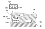
- FIG. 6 is a diagram for explaining a method of polishing a substrate according to one embodiment.
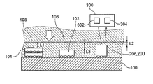
- FIG. 6 is a diagram for explaining a method of polishing a substrate according to one embodiment.
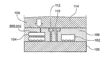
- FIG. 6 is a diagram for explaining a method of polishing a substrate according to one embodiment.
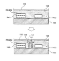
- FIG. 6 is a diagram for explaining a method of polishing a substrate according to one embodiment.
- FIG. 6 is a diagram for explaining a method of polishing a substrate according to one embodiment.
- FIG. 6 is a diagram for explaining a method of polishing a substrate according to one embodiment.
- FIG. 6 is a diagram for explaining a method of polishing a substrate according to one embodiment.
- FIG. 6 is a diagram for explaining a method of polishing a substrate according to one embodiment.
- FIG. 6 is a diagram for explaining a method of polishing a substrate according to one embodiment.
- FIG. 6 is a diagram for explaining a method of polishing a substrate according to one embodiment.
- FIG. 6 is a diagram for explaining a method of polishing a substrate according to one embodiment. It is a conceptual diagram showing composition of a CMP device by one embodiment.
- FIG. 4 is a cross-sectional view schematically illustrating an optical endpoint detection mechanism, according to one embodiment.
- FIG. 6 is a diagram for explaining a method of polishing a substrate according to one embodiment.
- FIG. 4 is a cross-sectional view schematically illustrating an optical endpoint detection mechanism, according to one embodiment.
- FIG. 4 is a cross-sectional view schematically illustrating an optical endpoint detection mechanism, according to one embodiment.
- FIG. 4 is a cross-sectional view schematically illustrating an optical endpoint detection mechanism, according to one embodiment.
- FIG. 4 is a cross-sectional view schematically illustrating an optical endpoint detection mechanism, according to one embodiment.
- FIG. 4 is a cross-sectional view schematically illustrating an optical endpoint detection mechanism, according to one embodiment. It is the figure which expanded the adapter vicinity of the optical end point detection mechanism shown by FIG. 17A. It is the figure which expanded the adapter vicinity of the optical end point detection mechanism shown by FIG. 17A.
- FIG. 1 is a view for explaining a method of polishing a substrate according to one embodiment.
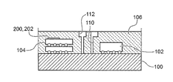
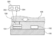
- the substrate is disposed on a copper clad laminate (CCL) base 100, a logic chip 102 such as a CPU or a GPU, and / or a memory chip 104 or the like.
- a chip having a predetermined function such as a logic chip or a memory chip is referred to as a functional chip.
- the end point detection element 200 is disposed on the upper surface of the functional chip located at the highest position from the surface of the CCL base 100 among the functional chips 102 and 104.
- FIG. 1 is a view for explaining a method of polishing a substrate according to one embodiment.
- the substrate is disposed on a copper clad laminate (CCL) base 100, a logic chip 102 such as a CPU or a GPU, and / or a memory chip 104 or the like.
- a chip having a predetermined function such as a logic chip or a memory chip is referred to as
- the endpoint detection element 200 is a reflective film 202 and is disposed on the memory chip 104.
- the reflective film 202 can be, for example, a coating of a metal film provided on the top surface of the functional chip.
- the CCL base 100 on which the functional chips 102 and 104 are mounted is sealed by the insulating material 106.
- the insulating material 106 can be made of, for example, a resin or a glass material. After sealing with the insulating material 106, the insulating material 106 is polished so that the insulating material 106 is flat.
- the polishing of the insulating material 106 can be chemical mechanical polishing (CMP).
- CMP can use a general CMP apparatus.
- the CMP apparatus can be arbitrary, and for example, a known CMP apparatus may be used.
- the endpoint detection element 200 can be used to detect the polishing endpoint. In the embodiment of FIG. 1, since the end point detection element 200 is the reflective film 202, the end point detection can be performed optically.
- the CMP apparatus 300 includes a light source 302 for irradiating the reflecting film 202 with light such as a laser, and further includes a sensor 304 for receiving reflected light from the reflecting film 202.
- the distance from the reflective film 202 is measured by the reflected light from the reflective film 202, and when polishing is performed to the polishing target position 108, the polishing is finished.
- the end point position of the insulating material 106 is desirably, for example, ⁇ 10 ⁇ m or less from the polishing target position 108.
- the polishing target position 108 can be, for example, 10 ⁇ m to 500 ⁇ m from the top surface of the chip at the uppermost position where the reflective film 202 is provided.
- the reflective film 202 is used as the end point detection element 200.
- a fluorescent material or a resin containing a fluorescent material is used instead of the reflective film 202. It can be used.
- the fluorescent material or the resin containing the fluorescent material may be applied only to the upper surface of the functional chip located at the highest position from the surface of the CCL base 100 as shown in FIG. After disposing the sexing chips 102, 104, it may be applied to the entire surface of the substrate.
- a fluorescent material or a resin containing a fluorescent material is applied to the upper surface of the functional chips 102 and 104, it may be applied to only a part of the surface or may be applied to the entire surface.
- the entire substrate is sealed with an insulating material 106.
- light source 302 is selected to include those wavelengths that cause the fluorescent material to fluoresce.
- the sensor 304 measures the intensity of the fluorescence from the fluorescent material applied to the top surface of the functional chip at the highest position. The intensity of the fluorescence changes with the thickness of the insulating material 106 disposed on the fluorescent material. Therefore, the thickness of the insulating material 106 can be detected based on the intensity of the detected fluorescence, and the end point of the polishing of the insulating material 106 can be detected.
- a wavelength filter can be used to detect only the fluorescence wavelength by the sensor 304.
- a spectroscope may be used to detect the intensity of the fluorescence wavelength.
- FIG. 2 is a diagram illustrating a method of polishing a substrate, according to one embodiment.
- the reflector 204 is provided on the upper surface of the functional chip 102, 104 located at the highest position from the surface of the CCL base 100 among the functional chips 102, 104. Fix it.
- the reflector 204 can be fixed to the top surface of the functional chip 102, 104 using, for example, an adhesive.
- the reflecting plate 204 can be, for example, a plate-like member provided with a metal coating. Except for the reflecting plate 204, the embodiment can be the same as the embodiment shown in FIG.
- FIG. 3 is a diagram illustrating a method of polishing a substrate, according to one embodiment.
- the substrate is disposed on a copper clad laminate (CCL) base 100, a logic chip 102 such as a CPU or a GPU, and / or a memory chip 104 or the like.
- the dummy element 206 irrelevant to the function of the device formed on the substrate is arranged as the end point detection element 200.
- the dummy element 206 is arranged such that the upper surface is higher than the upper surface of the functional chip located at the highest position from the surface of the CCL base 100.
- the upper surface of the dummy element 206 may be a reflective film 202 as in the embodiment of FIG. 1, and a reflective plate 204 as in the embodiment of FIG. 2 may be attached to the upper surface of the dummy element 206.
- Dummy element 206 can be attached to CCL base 100 by an adhesive.
- the dummy element 206 may be bump bonded as with the other functional chips 102,104. By performing bump bonding in the same process as the other functional chips 102 and 104, it is possible to reduce the mounting error between the functional chips 102 and 104 and the dummy element 206.
- the dummy element 206 can be placed at any place, but needs to be provided at a place that does not disturb other functional chips.
- a plurality of dummy elements 206 may be arranged. After the functional chips 102 and 104 and the dummy element 206 are disposed on the CCL base 100, the CCL base 100 on which the functional chips 102 and 104 and the dummy element 206 are mounted is sealed by the insulating material 106.
- the insulating material 106 can be made of, for example, a resin or a glass material. After sealing with the insulating material 106, the insulating material 106 is polished so that the insulating material 106 is flat.
- the polishing of the insulating material 106 can be chemical mechanical polishing (CMP).
- CMP can use a general CMP apparatus.
- the CMP apparatus can be arbitrary, and for example, a known CMP apparatus may be used.
- the end point of polishing can be detected using the dummy element 206 which is the end point detecting element 200.
- the end point detection can be performed optically as described above.
- the polishing target position 108 for example, as shown in FIG. 3, a distance L1 from the upper surface of the functional chip located at the highest position from the surface of the CCL base 100 is determined.
- the height difference L3 between the upper surface of the functional chip located at the highest position from the surface of the CCL base 100 and the upper surface of the dummy element 206 is measured.
- Such height difference L3 can be measured by any position sensor, confocal microscope or the like before functional chip 102, 104 and dummy element 206 are disposed on CCL base 100 and molded with insulating material 106. Can. Then, the distance L2 of the polishing target position 108 from the upper surface of the dummy element 206 is calculated so that the polishing target position 108 becomes L1. By polishing the insulating material 106 until the distance from the upper surface of the dummy element 206 to the surface of the insulating material 106 becomes L2 when polishing the insulating material 106, the insulating material 106 is polished to the polishing target position 108 It can be carried out.
- the polishing target position 108 at the end point can be, for example, 10 ⁇ m to 500 ⁇ m from the top surface of the chip at the uppermost position where the reflective film 202 is provided.
- FIG. 4 illustrates a method of polishing a substrate according to one embodiment.
- FIG. 4 shows a method for forming a wiring layer on the planarized insulating material 106 and polishing the wiring layer.
- the insulating material 106 is polished to the polishing target position 108 in the same manner as the embodiment shown in FIGS.
- the planarized dielectric 106 is then patterned for wiring.
- formation of a via 110 for vertical wiring, formation of a horizontal wiring pattern 112 and the like are performed by exposure, etching or the like.
- a metal layer 114 such as copper, is deposited over the patterned insulating material 106 (as shown in FIG. 4).
- target polishing location 108 may define target polishing location 108 to remove metal layer 114 and to polish a portion of insulating material 106.
- the polishing target position 108 can be set on the side of the insulating material 106 by about 5 ⁇ m to 10 ⁇ m from the interface between the metal layer 114 and the layer of the insulating material 106.
- the end point of polishing can be detected by observing a change in the eddy current with an eddy current sensor that detects an eddy current generated in the metal layer 114.
- the end point detection may be performed by observing a change in reflected light from the metal layer 114 with an optical sensor.
- the end point detection can be performed by observing a change in polishing resistance generated when the material changes from the metal layer 114 to the insulating material 106 or a change in torque of the drive mechanism of the CMP apparatus.
- the polishing is performed only for a predetermined time so as to prevent the remaining metal from being generated on the surface after polishing, and polishing may be performed up to the target polishing position 108 described above. Good. Other known end point detection may be adopted.
- FIG. 5 illustrates a method of polishing a substrate according to one embodiment.
- the insulating material 106 is polished to the polishing target position 108 in the same manner as the embodiment shown in FIGS.
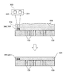
- the barrier mold layer 116 is then formed on the planarized insulating material 106 (the state of the upper diagram in FIG. 5).
- the barrier mold layer 116 is formed of an insulating material.
- the barrier mold layer 116 uses a material having a weight density different from that of the underlying insulating material 106 so that the frictional force at the time of polishing differs between the barrier mold layer 116 and the insulating material 106.
- the barrier mold layer 116 can be thinner than the layer of the insulating material 106.
- the barrier mold layer 116 can have a thickness of about 10 nm to 10 ⁇ m.
- the polishing resistance changes when the metal layer 114 is removed and the barrier mold layer 116 is exposed. Therefore, the change in polishing resistance can be used to detect the end point of polishing for removing the metal layer 114 by CMP.
- the barrier mold layer 116 is removed by over-polishing, the lower insulating material 106 is exposed, and the polishing resistance is further changed. Therefore, over-polishing can be detected from the change in polishing resistance when changing from the barrier mold layer 116 to the insulating material 106.
- FIG. 6 is a diagram illustrating a method of polishing a substrate according to one embodiment.
- the insulating material 106 is polished to the polishing target position 108 in the same manner as the embodiment shown in FIGS.
- the planarized dielectric 106 is then patterned for wiring.
- As a pattern for wiring formation of a via 110 for vertical wiring, formation of a horizontal wiring pattern 112 and the like are performed by exposure, etching or the like (state in FIG. 6).
- the hydrophilicity of the surface of the insulating material 106 is improved by light or laser exposure. This treatment can improve the adhesion of the metal layer 114 which is a conductive material, which is performed later.
- the subsequent formation of the metal layer 114 and the like can be the same as in the embodiment described with reference to FIG. Moreover, you may add the process which improves hydrophilicity to embodiment described in FIG. 5, or other embodiment.
- FIG. 7 is a diagram illustrating a method of polishing a substrate according to one embodiment.
- the substrate has a copper clad laminate (CCL) base 100 provided with the through wiring 150.
- the CCL base 100 including the through wiring 150 is planarized by CMP or the like.
- the end point detection element 200 is disposed on the upper surface of the CCL base 100 which is planarized.
- the endpoint detection element 200 is a reflector 204.
- the reflector 204 can be fixed on the CCL base 100 using, for example, an adhesive. Thereafter, the CCL base 100 on which the reflection plate 204 is disposed is sealed by the insulating material 106.
- the insulating material 106 can be, for example, a resin or a glass material, as described above. After sealing with the insulating material 106, the insulating material 106 is polished so that the insulating material 106 is flat. The end point detection of the polishing of the insulating material 106 can be performed by detecting reflected light of light or a laser with a sensor as described above with reference to FIGS.
- the position of the reflecting plate 204 is arbitrary, but needs to be a position which does not disturb other functional chips or the like. Further, a plurality of reflecting plates 204 may be provided. Further, in the embodiment of FIG. 7, the dummy element 206 shown in FIG. 3 may be provided in place of the reflection plate 204.
- FIG. 8 illustrates a method of polishing a substrate according to one embodiment.
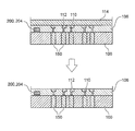
- FIG. 8 shows a method for forming a wiring layer on the planarized insulating material 106 and polishing the wiring layer.
- the insulating material 106 is polished to the polishing target position 108 in the same manner as the embodiment shown in FIG.
- the planarized dielectric 106 is then patterned for wiring.
- formation of a via 110 for vertical wiring, formation of a horizontal wiring pattern 112 and the like are performed by exposure, etching or the like.
- a metal layer 114 such as copper, which is a conductive material, for example, is deposited on the patterned insulating material 106 (as shown in the upper illustration of FIG. 8). Thereafter, unnecessary portions of the metal layer 114 are polished and removed.
- the polishing of the metal layer 114 can be performed by CMP. Polishing of the metal layer 114 can be similar to that described in the embodiment of FIG.
- FIG. 9 illustrates a method of polishing a substrate according to one embodiment.
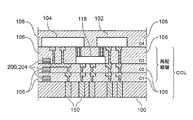
- FIG. 9 shows a method for forming a plurality of layers of insulating material 106 provided with a wiring layer.
- the first layer C1 of the insulating material 106 formed on the CCL base 100 can be formed in the same manner as the embodiment shown in FIG. Thereafter, the reflecting plate 204 is fixed to the upper surface of the planarized first layer C1.
- the reflector 204 can be fixed to the top surface of the first layer C1 using, for example, an adhesive.
- the insulating material 106 is formed, and as described in FIG. 8, the wiring pattern is formed, the metal layer 114 is formed, and the metal layer 114 is polished to form the second layer C2.
- the third layer C3 can be formed in the same manner. Any number of layers of the insulating material 106 including the wiring layer can be formed.
- functional chips such as the logic chip 102 and the memory chip 104 are disposed on the third layer C3.
- wiring between these functional chips may be performed by an interconnect chip 118 or an interposer.
- FIG. 9 shows an example in which the wiring and the functional chip are mounted on only one side of the CCL base 100, it may be mounted on both sides of the CCL base 100 as another embodiment.
- vertical wiring may be formed for extracting the wiring from the interposer or the interconnect chip 118 to the outside of the package mold.
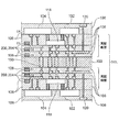
- FIG. 10 shows an example in which wires and functional chips are mounted on both surfaces of the CCL base 100, and vertical wires 120 for extracting the wires from the interconnect chip 118 to the outside of the package mold are provided.
- the package shown in FIG. 10 can be formed by combining the methods disclosed herein.
- FIG. 11 is a conceptual view showing the configuration of a CMP apparatus 300 according to an embodiment.
- the CMP apparatus 300 includes a substrate holding head 21, a bearing ball 3, a head shaft 2, a polishing plate 38, a polishing pad 39, a first air supply line 36, a second air supply line 62, a first air regulator R1, and a second air regulator. R2, a pure water supply line 46, and a pure water regulator R4 are provided.
- the polishing apparatus 1 further includes a head fixing member 4, a connecting shaft 48, an air cylinder 5, a piston 14, a third air supply line 51, a third air regulator R 3, a rotating cylinder 6, a timing pulley 7, a timing belt 8 and a timing pulley 10. ,
- the motor 9 the abrasive liquid supply nozzle 13 and the like.
- the substrate holding head 21 is engaged with the head shaft 2 via a bearing ball 3.
- the head shaft 2 is engaged with the head fixing member 4 via a bearing (not shown) so as to freely move up and down and rotatably, and is connected to the piston 14 in the air cylinder 5 via the connecting shaft 48 and the connecting rod 61.
- the air cylinder 5 is connected to the third air supply line 51.
- the third air supply line 51 is connected to the compressed air source 42 via the third valve V3 and the third air regulator R3.
- the pressure of the air cylinder 5 is controlled to a predetermined pressure by the third air regulator R3.
- the pressure of the air cylinder 5 vertically moves the piston 14, and the vertical movement of the piston 14 vertically moves the connecting shaft 48 and the substrate holding head shaft 2 via the connecting rod 61 and is held by the lower surface of the substrate holding head 21.
- the substrate W is separated from the polishing plate 38 or pressed against the polishing plate 38.
- the upper surface of the substrate holding head 21 and the lower end surface of the head shaft 2 form a ball bearing that accommodates the bearing ball 3, and the substrate holding head 21 is also polished to the polishing disc 38 via the bearing ball 3.
- the cloth 39 can be tilted about the bearing ball 3.
- the bearing ball 3 is located at the center of the head shaft 2.
- a rotary cylinder 6 is attached to the head shaft 2, and the rotary cylinder 6 is provided with a timing pulley 7 on the outer periphery thereof.
- the timing pulley 7 is connected via a timing belt 8 to a timing pulley 10 provided to a motor 9 fixed to a head fixing member 4 (also referred to as an arm). Therefore, by driving the motor 9 to rotate, the rotary cylinder 6 and the head shaft 2 integrally rotate via the timing belt 8 and the timing pulley 7, and the substrate holding head 21 is rotated by the rotation of the head shaft 2.
- one end of the head fixing member 4 is supported by a swing shaft 64 and is swingable. The rotation from the head shaft 2 is not transmitted to the connecting shaft 48.
- the CMP apparatus 300 has a control apparatus 900, and various sensors and operation mechanisms provided in the CMP apparatus 300 can be configured to be controlled by the control apparatus 900.
- the control device 900 can be configured from a general computer provided with an input / output device, an arithmetic device, a storage device, and the like.
- the control device is installed with a computer program for operating the method described herein.
- the computer program may be stored in a non-volatile storage medium, or may be distributed to computers using various communication techniques.
- the substrate to be polished is held on the lower surface of the substrate holding head 21 by vacuum suction.
- a polishing disk 38 is disposed below the substrate holding head 21 in the vertical direction.
- a polishing pad 39 is attached to the upper surface of the polishing plate 38.
- the polishing pad 39 is configured to be in contact with the surface to be polished of the substrate.
- the surface of the polishing pad 39 in contact with the surface to be polished of the substrate W is a polishing surface.
- the substrate holding head 21 is connected to the air supply line 62.
- the air supply line 62 is connected to a compressed air source 42 via a valve V2 and an air regulator R2, and is connected to a vacuum exhaust source 49 via a valve V0.
- a desired pressure can be applied to the back surface (surface opposite to the surface to be polished) of the substrate held by the substrate holding head 21, and this pressure
- the substrate is pressed toward the polishing plate 38.
- opening the valve V0 in a state in which the valve V2 is closed the back surface of the substrate held by the substrate holding head 21 can be vacuumed, and the substrate W can be vacuum-sucked to the substrate holding head 21.
- the polishing disc 38 can include a sensor 100 for detecting the end point of polishing of the substrate.
- FIG. 12 is a cross-sectional view that schematically illustrates an optical endpoint detection mechanism, according to one embodiment.
- FIG. 12 shows the portion of the polishing disk 38 where the sensor 304 is provided.
- a sensor 304 shown in FIG. 12 is an optical sensor, and a light source 302 is further disposed on the polishing disk 38.
- the sensor 304 and the light source 302 are configured to be able to communicate with the control device 900 (FIG. 11) by wire or wirelessly.
- a notch 39-2 is provided in a part of the polishing pad 39.
- sensor 304 may comprise a spectrometer, such as, for example, a Fabry-Perot spectrometer.
- a fiber sensor is used as the sensor 304, a plurality of sensors 304 and light sources 302 may be arranged on the polishing disk 38.
- the polishing disc 38 may be located at the center and periphery of the polishing disc 38 and the signals from both sensors 304 and light sources 302 may be monitored to determine the polishing endpoint of the substrate W. Further, by using the plurality of sensors 304 and the light sources 302, the film thickness of the polished surface of the plurality of regions of the substrate W can be monitored. The polishing conditions can be controlled based on the signals from the plurality of sensors 304 so that the polishing end points of the plurality of regions of the substrate W become the same period.
- the CMP apparatus 300 shown in FIG. 11 and the end point detection sensor shown in FIG. 12 can be used in the above-described method of polishing a substrate and a method of detecting an end point of substrate polishing. Also, the CMP apparatus 300 shown in FIG. 11 and the end point detection sensor shown in FIG. 12 can be used in a method of detecting the end point of substrate polishing by another method. Several methods for detecting the end point of substrate polishing will be described below.
- FIG. 13 illustrates a method of polishing a substrate according to one embodiment.
- the substrate is disposed on a copper clad laminate (CCL) base 100, a logic chip 102 such as a CPU or a GPU, and / or a memory chip 104 or the like.
- the substrate shown in FIG. 13 is not provided with the end point detection element 200 such as the reflective film 202.
- the insulating material 106 can be made of, for example, a resin or a glass material.
- polishing of the insulating material 106 can be performed by chemical mechanical polishing (CMP), for example, using a CMP apparatus 300 including an optical end point detection sensor shown in FIG.
- CMP chemical mechanical polishing
- the reflected light can be dispersed to measure the thickness of the insulating material 106 from the relative reflectance for each wavelength of the reflected light.
- the light emitted from the light source 302 toward the insulating material 106 of the substrate is reflected by the surface of the insulating material 106, and is also at the surface of the functional chip (memory chip 104 in the example of FIG. 13) at the highest position. It will be reflected. Interference of light reflected at different positions causes the relative reflectance of each of the wavelengths of light detected by the sensor 304 to change in accordance with the thickness of the insulating material 106. Therefore, the thickness of the insulating material 106 on the functional chips 102 and 104 can be measured by detecting the relative reflectance.
- the light source 302 and the sensor 304 shown in FIG. It can be used.
- the polishing target position 108 the polishing is finished.
- the end point position of the insulating material 106 is desirably, for example, ⁇ 10 ⁇ m or less from the polishing target position 108.
- the polishing target position 108 can be, for example, 10 ⁇ m to 500 ⁇ m from the top surface of the tip 104 at the uppermost position.
- a Fabry-Perot spectrometer or the like can be used.
- the light source 302 can use any light source such as a laser diode or an LED.
- the wavelength range of light source 302 may include, for example, 500 nm to 800 nm. Further, as the wavelength of the light source 302, it is also possible to use a short wavelength range of 200 nm to 500 nm according to the film thickness and film type of the insulating material 106 to be irradiated.
- the above-mentioned method detects the end point of substrate polish from change of relative reflectance of catoptric light about Drawing 13 concerning the light intensity, it can also detect the end point of substrate polish by measuring intensity.
- light is emitted from the light source 302 to the functional chips 102 and 104 located at the highest position on the substrate, and the reflected light is detected by the sensor 304. Since the intensity of the reflected light changes according to the thickness of the insulating material 106 disposed on the functional chips 102 and 104, the reflection when the thickness of the insulating material 106 reaches the polishing target position 108 in advance by preliminary experiments By measuring the light intensity, the light source 302 and the sensor 304 shown in FIG.
- the light source 302 can be any light source such as a laser diode or an LED.
- the light source 302 preferably includes a wavelength range (for example, a wavelength of 500 nm or less) having a high reflectance on the surface (for example, silicon) of the functional chips 102 and 104.
- a monochromatic light source of a specific wavelength for example, any wavelength of 500 nm or less may be used.
- infrared light for example, a wavelength of 1 ⁇ m to 3 ⁇ m
- an infrared spectrometer to detect the thickness of the insulating material 106 and the end point of polishing You can also.
- the reflectance of infrared light on the surfaces of the functional chips 102 and 104 is different from the reflectance of infrared light on the surface of the insulating material 106 (for example, resin). Therefore, depending on the thickness of the insulating material 106 formed on the functional chips 102 and 104, the spectral intensity of the reflected light received by the sensor 304 changes. Therefore, the thickness of the insulating material 106 can be detected by the spectrum change of the reflected light.
- FIG. 14 is a cross-sectional view that schematically illustrates an optical endpoint detection mechanism, according to one embodiment.
- FIG. 14 shows the portion of the polishing disk 38 where the sensor 304 is provided.
- the end point detection mechanism shown in FIG. 14 includes two light sources 302a and 302b. Each light source 302a, 302b is positioned to emit light towards the surface of the substrate (not shown) being polished.
- the sensor 304 is positioned to receive scattered light of the light emitted to the substrate.
- the endpoint detection mechanism according to the embodiment shown in FIG. 14 may comprise a spectrometer.
- the sensor 304 and the light source 302 are configured to be able to communicate with the control device 900 (FIG. 11) by wire or wirelessly.
- FIG. 11 the control device 900
- a part of the polishing pad 39 is provided with a notch 39-2. Position the viewport 306 at the position of the notch 39-2.
- light may be directed from the light source 302 towards the substrate being polished via the viewport 306 and scattered light from the substrate may be detected by the sensor 304.
- the view port 306 may not be provided, in which case detection is performed while supplying pure water to the recess of the polishing disc 38 in which the light sources 302a and 302b and the sensor 304 are disposed.
- the end point detection mechanism according to the embodiment shown in FIG. 14 can be used for the above-mentioned polishing method and end point detection.
- FIG. 15 is a cross-sectional view that schematically illustrates an optical endpoint detection mechanism, according to one embodiment.
- FIG. 15 shows the portion of the polishing disk 38 where the sensor 304 is provided.
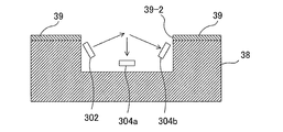
- the end point detection mechanism shown in FIG. 15 includes one light source 302, a first sensor 304a, and a second sensor 304b.
- the light source 302 is positioned to illuminate the substrate at an angle that results in total reflection at the surface of the substrate.
- the second sensor 304 b is positioned to receive the totally reflected light.
- the first sensor 304a is positioned to receive light scattered on the surface of the substrate.
- FIG. 15 shows the portion of the polishing disk 38 where the sensor 304 is provided.
- the end point detection mechanism shown in FIG. 15 includes one light source 302, a first sensor 304a, and a second sensor 304b.
- the light source 302 is positioned to illuminate the substrate at an angle that results in total reflection at the surface of the substrate.
- the second sensor 304 b is positioned
- the light source 302 and the second sensor 304b can include a drive mechanism (not shown) capable of adjusting the incident angle of light on the surface of the substrate.
- the end point detection mechanism using total reflection shown in FIG. 15 can be used when the material changes at the target polishing position. For example, as described in conjunction with FIG. 4 and FIG. 8, it can be used to remove the metal layer 114 laminated on the insulating material 106. Since the total reflection angle at the metal layer 114 is different from the total reflection angle when the metal layer 114 is removed and the underlying insulating material 106 is exposed, the metal layer 114 is removed from the change in received light intensity. Can be detected.
- the light totally reflected by the second sensor 304 b may be measured, the scattered light may be measured by the first sensor 304 a, or both may be measured.
- detection can be performed while supplying pure water to the recess of the polishing disc 38 in which the light source 302 and the sensors 304a and 304b are disposed.
- the relationship between the refractive index A of the medium in contact with the surface to be polished such as water or pure water and the refractive index B of the substrate surface such as the insulating material 106 satisfies: refractive index A> refractive index B
- FIG. 16 is a cross-sectional view that schematically illustrates an optical endpoint detection mechanism, according to one embodiment.
- FIG. 16 shows a portion of the polishing disk 38 where the sensor 304 is provided.
- the endpoint detection mechanism shown in FIG. 16 utilizes total internal reflection similar to the embodiment shown in FIG.
- the light emitted from the light source 302 is reflected by the first mirror 308a and guided to the surface of the substrate.
- the first mirror 308a is positioned to direct light to the substrate at an angle that causes total reflection at the surface of the substrate.
- the end point detection mechanism shown in FIG. 16 includes a second mirror 308 b.
- the second mirror 308 b is positioned to direct the light totally reflected on the surface of the substrate being polished to the second sensor 304 b.
- the first mirror 308a and the second mirror 308b can include a driving mechanism (not shown) capable of adjusting the incident angle of light with respect to the surface of the substrate.
- the other end point detection mechanism of FIG. 16 may be the same as the end point detection mechanism shown in FIG. Similar to the end point detection mechanism shown in FIG. 15, the end point detection mechanism using total reflection shown in FIG. 16 can be used when the material changes at the target polishing position.
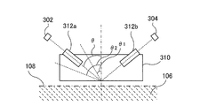
- FIG. 17A is a cross-sectional view that schematically illustrates an optical endpoint detection mechanism, according to one embodiment.
- FIG. 17A shows a portion of the polishing disk 38 where the sensor 304 is provided, but the polishing disk 38 and the pad 39 are not shown for clarity.
- the endpoint detection mechanism shown in FIG. 17A comprises a light source 302 and a sensor 304, as well as other optical endpoint detection mechanisms.
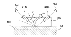
- the endpoint detection mechanism shown in FIG. 17A further comprises an adapter 310.
- the adapter 310 can be formed, for example, from a high refractive index material, such as an optical plastic.
- the refractive index of the adapter 310 is desirably larger than the refractive index of the insulating material 106 on the substrate surface to be polished.
- the adapter 310 can be a generally rectangular block.
- the adapter 310 can be placed in contact with or in proximity to the surface of the substrate to be polished.
- the adapter 310 is provided with a first optical fiber 312 a and a second optical fiber 312 b.
- the first optical fiber 312a and the light source 302 are arranged such that the light from the light source 302 is received by the first optical fiber 312a.
- the second optical fiber 312 b is disposed such that the light emitted from the first optical fiber 312 a receives the light reflected at the interface between the adapter 310 and the surface of the substrate.
- the second optical fiber 312b and the sensor 304 are arranged such that the sensor 304 receives the light emerging from the second optical fiber 312b.
- the first optical fiber 312a and the second optical fiber 312b may be optical fibers having the same diameter or may be optical fibers having different diameters.
- the second optical fiber 312b may be an optical fiber having a larger diameter than the first optical fiber 312a in order to increase the yield.
- an array type light sensor for example, a photodiode array
- the light source 302, the sensor 304, and the adapter 310 are configured to be movable in the direction perpendicular to the surface of the substrate while maintaining their relative positions. For example, they are attached to the polishing disc 38 by a moving mechanism (not shown).
- FIG. 17B is an enlarged view of the vicinity of the adapter 310 of the optical end point detection mechanism shown in FIG. 17A.
- the first optical fiber 312a is disposed such that the light emitted from the first optical fiber 312a is incident on the interface of the adapter 310 at an incident angle ⁇ .
- the incident angle ⁇ is larger than the critical angle ⁇ 1 determined from the refractive index of the adapter 310 and the refractive index of water or pure water, and the refractive index of the adapter 310 and the material of the substrate surface to be polished (for example, insulating material It is set to be smaller than a critical angle ⁇ 2 determined from the refractive index of 106).
- the optical endpoint detection mechanism shown in FIG. 17A can be used to detect the substrate polishing endpoint as follows.
- the substrate to be polished is a CCL (Copper Clad Laminate) base 100 on which a functional chip such as a logic chip 102 such as a CPU or GPU and / or a memory chip 104 is disposed.
- the CCL base 100 on which these functional chips 102 and 104 are disposed is sealed by an insulating material 106.
- the insulating material 106 can be made of, for example, a resin or a glass material.
- a method of polishing the insulating material 106 to the polishing target position 108 will be described using the end point detection mechanism shown in FIG. 17A.
- the adapter 310 is moved in the direction of the substrate until the adapter 310 contacts the surface of the substrate.
- the position of the adapter 310 in the direction perpendicular to the substrate surface is fixed.
- the surface of the substrate is roughly polished to planarize the surface of the substrate.
- the adapter 310 is again moved toward the substrate to bring the adapter 310 into intimate contact with the planarized surface of the substrate.
- the polishing amount by rough polishing can be calculated from the movement distance of the adapter 310.
- the amount of rough polishing may be calculated by measuring the distance between the position of the adapter 310 at the start of rough polishing and the planarized substrate surface by another method.
- FIGS. 17A and 17B show this state. Polishing is further performed in this state. At this time, light is emitted from the light source 302 toward the surface of the substrate through the first optical fiber 312a. The amount of polishing of the substrate can be measured by detecting the reflected light through the second optical fiber 312 b with the sensor 304. As shown in FIG. 17B, the adapter 310 is in contact with the insulating material 106 on the surface of the substrate in the state of starting the polishing.
- the incident angle ⁇ of light is larger than the critical angle ⁇ 1 determined from the refractive index of the adapter 310 and the refractive index of water or pure water, the light is totally reflected at the boundary between the adapter 310 and pure water . Therefore, as the polishing progresses, the intensity of the reflected light detected by the sensor 304 increases.
- the amount of polishing can be determined from the change in the intensity of the reflected light detected by the sensor 304.
- the insulating material 106 can be polished to the polishing target position 108.
- the semiconductor material such as Si or SiO 2 can be applied to the polishing end point detection as described above.
Landscapes
- Engineering & Computer Science (AREA)
- Mechanical Engineering (AREA)
- Mechanical Treatment Of Semiconductor (AREA)
- Constituent Portions Of Griding Lathes, Driving, Sensing And Control (AREA)
- Finish Polishing, Edge Sharpening, And Grinding By Specific Grinding Devices (AREA)
Priority Applications (5)
| Application Number | Priority Date | Filing Date | Title |
|---|---|---|---|
| KR1020237021860A KR102770137B1 (ko) | 2017-09-05 | 2018-08-22 | 기능성 칩을 구비하는 기판을 연마하는 방법 |
| CN201880057226.1A CN111095492B (zh) | 2017-09-05 | 2018-08-22 | 基板、具备功能性芯片的基板的研磨方法、非暂时性的计算机可读取的记录介质 |
| KR1020207005105A KR102550564B1 (ko) | 2017-09-05 | 2018-08-22 | 기능성 칩을 구비하는 기판을 연마하는 방법 |
| US16/643,124 US11597051B2 (en) | 2017-09-05 | 2018-08-22 | Method for polishing substrate including functional chip |
| US18/161,707 US20230173636A1 (en) | 2017-09-05 | 2023-01-30 | Method for polishing substrate including functional chip |
Applications Claiming Priority (2)
| Application Number | Priority Date | Filing Date | Title |
|---|---|---|---|
| JP2017-170302 | 2017-09-05 | ||
| JP2017170302A JP6860451B2 (ja) | 2017-09-05 | 2017-09-05 | 機能性チップを備える基板を研磨する方法 |
Related Child Applications (2)
| Application Number | Title | Priority Date | Filing Date |
|---|---|---|---|
| US16/643,124 A-371-Of-International US11597051B2 (en) | 2017-09-05 | 2018-08-22 | Method for polishing substrate including functional chip |
| US18/161,707 Division US20230173636A1 (en) | 2017-09-05 | 2023-01-30 | Method for polishing substrate including functional chip |
Publications (1)
| Publication Number | Publication Date |
|---|---|
| WO2019049659A1 true WO2019049659A1 (ja) | 2019-03-14 |
Family
ID=65633980
Family Applications (1)
| Application Number | Title | Priority Date | Filing Date |
|---|---|---|---|
| PCT/JP2018/030894 Ceased WO2019049659A1 (ja) | 2017-09-05 | 2018-08-22 | 機能性チップを備える基板を研磨する方法 |
Country Status (6)
| Country | Link |
|---|---|
| US (2) | US11597051B2 (enExample) |
| JP (2) | JP6860451B2 (enExample) |
| KR (2) | KR102550564B1 (enExample) |
| CN (1) | CN111095492B (enExample) |
| TW (1) | TWI773810B (enExample) |
| WO (1) | WO2019049659A1 (enExample) |
Families Citing this family (3)
| Publication number | Priority date | Publication date | Assignee | Title |
|---|---|---|---|---|
| JP7325913B2 (ja) * | 2019-11-22 | 2023-08-15 | 株式会社ディスコ | ウェーハ加工装置 |
| JP7693393B2 (ja) | 2021-05-24 | 2025-06-17 | キオクシア株式会社 | 半導体装置の製造方法 |
| KR20230117970A (ko) | 2022-02-03 | 2023-08-10 | 삼성전자주식회사 | 다층 광학 박막 구조를 포함하는 광학 장치 및 다층 광학 박막 구조의 평탄화 방법 및 장치 |
Citations (5)
| Publication number | Priority date | Publication date | Assignee | Title |
|---|---|---|---|---|
| JP2000124601A (ja) * | 1998-10-13 | 2000-04-28 | Ibiden Co Ltd | プリント配線板の製造方法 |
| JP3141939B2 (ja) * | 1998-11-26 | 2001-03-07 | 日本電気株式会社 | 金属配線形成方法 |
| JP4056854B2 (ja) * | 2002-11-05 | 2008-03-05 | 新光電気工業株式会社 | 半導体装置の製造方法 |
| US20150258657A1 (en) * | 2011-11-07 | 2015-09-17 | Taiwan Semiconductor Manufacturing Company, Ltd. | Grinding Wheel Design with Elongated Teeth Arrangement |
| JP6005467B2 (ja) * | 2011-10-26 | 2016-10-12 | 株式会社荏原製作所 | 研磨方法および研磨装置 |
Family Cites Families (21)
| Publication number | Priority date | Publication date | Assignee | Title |
|---|---|---|---|---|
| JPS628981A (ja) * | 1985-07-04 | 1987-01-16 | Daido Steel Co Ltd | 巻取ドラムアダプタ |
| US5234868A (en) * | 1992-10-29 | 1993-08-10 | International Business Machines Corporation | Method for determining planarization endpoint during chemical-mechanical polishing |
| KR0166848B1 (ko) * | 1995-04-07 | 1999-02-01 | 문정환 | 반도체 제조시의 연마종점 설정방법 및 장치 |
| JPH09139369A (ja) * | 1995-11-15 | 1997-05-27 | Hitachi Ltd | 半導体装置の製造方法およびそれに使用される研磨装置 |
| MY139405A (en) * | 1998-09-28 | 2009-09-30 | Ibiden Co Ltd | Printed circuit board and method for its production |
| JP3774094B2 (ja) * | 1999-12-02 | 2006-05-10 | 株式会社日立製作所 | 膜厚、加工深さ測定装置及び成膜加工方法 |
| JP2002246352A (ja) * | 2001-02-20 | 2002-08-30 | Semiconductor Leading Edge Technologies Inc | Cmp終点検出装置、cmp終点検出方法、及びcmp研磨面モニタ方法 |
| US20050173259A1 (en) * | 2004-02-06 | 2005-08-11 | Applied Materials, Inc. | Endpoint system for electro-chemical mechanical polishing |
| JP2007214402A (ja) | 2006-02-10 | 2007-08-23 | Cmk Corp | 半導体素子及び半導体素子内蔵型プリント配線板 |
| JP4899604B2 (ja) | 2006-04-13 | 2012-03-21 | ソニー株式会社 | 三次元半導体パッケージ製造方法 |
| KR101357290B1 (ko) * | 2006-10-06 | 2014-01-28 | 가부시끼가이샤 도시바 | 가공 종점 검지방법, 연마방법 및 연마장치 |
| JP2008100319A (ja) * | 2006-10-19 | 2008-05-01 | Sharp Corp | 研削加工方法および研削加工装置 |
| JP2011000647A (ja) * | 2009-06-16 | 2011-01-06 | Ebara Corp | 研磨監視方法 |
| TWI453837B (zh) * | 2011-06-13 | 2014-09-21 | 日月光半導體製造股份有限公司 | 具有非導電層的半導體封裝及其製造方法 |
| JP2013044782A (ja) * | 2011-08-22 | 2013-03-04 | Seiko Epson Corp | 光学素子、電気光学装置、投射型映像装置及び光学素子の製造方法 |
| CN103814439B (zh) | 2011-09-09 | 2016-10-19 | 株式会社村田制作所 | 模块基板 |
| JP6157890B2 (ja) * | 2013-03-26 | 2017-07-05 | 日東電工株式会社 | アンダーフィル材、封止シート及び半導体装置の製造方法 |
| US9490186B2 (en) * | 2013-11-27 | 2016-11-08 | Applied Materials, Inc. | Limiting adjustment of polishing rates during substrate polishing |
| TWI591764B (zh) * | 2015-01-12 | 2017-07-11 | 精材科技股份有限公司 | 晶片封裝體及其製造方法 |
| US9595492B2 (en) * | 2015-03-16 | 2017-03-14 | Taiwan Semiconductor Manufacturing Company Ltd. | Device manufacture and packaging method thereof |
| US9754805B1 (en) * | 2016-02-25 | 2017-09-05 | Taiwan Semiconductor Manufacturing Company, Ltd. | Packaging method and structure |
-
2017
- 2017-09-05 JP JP2017170302A patent/JP6860451B2/ja active Active
-
2018
- 2018-08-22 WO PCT/JP2018/030894 patent/WO2019049659A1/ja not_active Ceased
- 2018-08-22 US US16/643,124 patent/US11597051B2/en active Active
- 2018-08-22 KR KR1020207005105A patent/KR102550564B1/ko active Active
- 2018-08-22 CN CN201880057226.1A patent/CN111095492B/zh active Active
- 2018-08-22 KR KR1020237021860A patent/KR102770137B1/ko active Active
- 2018-08-28 TW TW107129857A patent/TWI773810B/zh active
-
2021
- 2021-03-26 JP JP2021053348A patent/JP7177207B2/ja active Active
-
2023
- 2023-01-30 US US18/161,707 patent/US20230173636A1/en not_active Abandoned
Patent Citations (5)
| Publication number | Priority date | Publication date | Assignee | Title |
|---|---|---|---|---|
| JP2000124601A (ja) * | 1998-10-13 | 2000-04-28 | Ibiden Co Ltd | プリント配線板の製造方法 |
| JP3141939B2 (ja) * | 1998-11-26 | 2001-03-07 | 日本電気株式会社 | 金属配線形成方法 |
| JP4056854B2 (ja) * | 2002-11-05 | 2008-03-05 | 新光電気工業株式会社 | 半導体装置の製造方法 |
| JP6005467B2 (ja) * | 2011-10-26 | 2016-10-12 | 株式会社荏原製作所 | 研磨方法および研磨装置 |
| US20150258657A1 (en) * | 2011-11-07 | 2015-09-17 | Taiwan Semiconductor Manufacturing Company, Ltd. | Grinding Wheel Design with Elongated Teeth Arrangement |
Also Published As
| Publication number | Publication date |
|---|---|
| KR20230101949A (ko) | 2023-07-06 |
| KR20200049767A (ko) | 2020-05-08 |
| CN111095492A (zh) | 2020-05-01 |
| US20200391341A1 (en) | 2020-12-17 |
| TWI773810B (zh) | 2022-08-11 |
| KR102550564B1 (ko) | 2023-07-04 |
| CN111095492B (zh) | 2023-12-01 |
| US20230173636A1 (en) | 2023-06-08 |
| JP7177207B2 (ja) | 2022-11-22 |
| TW201919822A (zh) | 2019-06-01 |
| KR102770137B1 (ko) | 2025-02-20 |
| JP6860451B2 (ja) | 2021-04-14 |
| JP2019047022A (ja) | 2019-03-22 |
| US11597051B2 (en) | 2023-03-07 |
| JP2021103789A (ja) | 2021-07-15 |
Similar Documents
| Publication | Publication Date | Title |
|---|---|---|
| JP7177207B2 (ja) | 機能性チップを備える基板を研磨する方法 | |
| TWI538076B (zh) | 磨光裝置、磨光方法及磨光墊 | |
| JP5629690B2 (ja) | 半定量的な厚さの決定 | |
| US9799578B2 (en) | Peak-based endpointing for chemical mechanical polishing | |
| KR100715072B1 (ko) | 상이한 파장을 갖는 광선으로 종료점을 검출하는 방법 및 장치 | |
| US7938714B2 (en) | Polishing pad assembly with glass or crystalline window | |
| US20020127951A1 (en) | Method and apparatus for monitoring polishing state, polishing device, process wafer, semiconductor device, and method of manufacturing semiconductor device | |
| JP3327175B2 (ja) | 検知部及びこの検知部を具えたウェハ研磨装置 | |
| US6746319B2 (en) | Measuring apparatus | |
| JP2013219248A (ja) | 研磨装置および研磨方法 | |
| JP2019195891A (ja) | 研磨装置および研磨パッド | |
| US20010023167A1 (en) | Polishing apparatus | |
| JP2005340679A (ja) | 研磨装置及び研磨終点検出方法ならびに半導体装置の製造方法 | |
| JP7783107B2 (ja) | ワークピースの研磨方法および研磨装置 | |
| CN113664713A (zh) | 膜厚测定装置、研磨装置以及膜厚测定方法 | |
| JPH09298174A (ja) | 研磨方法及びそれを用いた研磨装置 | |
| JPH11204473A (ja) | 研磨加工方法および研磨加工装置 | |
| JPH09298175A (ja) | 研磨方法及びそれを用いた研磨装置 |
Legal Events
| Date | Code | Title | Description |
|---|---|---|---|
| 121 | Ep: the epo has been informed by wipo that ep was designated in this application |
Ref document number: 18853181 Country of ref document: EP Kind code of ref document: A1 |
|
| NENP | Non-entry into the national phase |
Ref country code: DE |
|
| 122 | Ep: pct application non-entry in european phase |
Ref document number: 18853181 Country of ref document: EP Kind code of ref document: A1 |