WO2019047489A1 - 铁电存储集成电路及其操作方法和制备方法 - Google Patents
铁电存储集成电路及其操作方法和制备方法 Download PDFInfo
- Publication number
- WO2019047489A1 WO2019047489A1 PCT/CN2018/077485 CN2018077485W WO2019047489A1 WO 2019047489 A1 WO2019047489 A1 WO 2019047489A1 CN 2018077485 W CN2018077485 W CN 2018077485W WO 2019047489 A1 WO2019047489 A1 WO 2019047489A1
- Authority
- WO
- WIPO (PCT)
- Prior art keywords
- ferroelectric
- electrode
- single crystal
- memory cell
- ferroelectric memory
- Prior art date
- Legal status (The legal status is an assumption and is not a legal conclusion. Google has not performed a legal analysis and makes no representation as to the accuracy of the status listed.)
- Ceased
Links
Images




Classifications
-
- G—PHYSICS
- G11—INFORMATION STORAGE
- G11C—STATIC STORES
- G11C11/00—Digital stores characterised by the use of particular electric or magnetic storage elements; Storage elements therefor
- G11C11/21—Digital stores characterised by the use of particular electric or magnetic storage elements; Storage elements therefor using electric elements
- G11C11/22—Digital stores characterised by the use of particular electric or magnetic storage elements; Storage elements therefor using electric elements using ferroelectric elements
- G11C11/225—Auxiliary circuits
- G11C11/2273—Reading or sensing circuits or methods
-
- H—ELECTRICITY
- H10—SEMICONDUCTOR DEVICES; ELECTRIC SOLID-STATE DEVICES NOT OTHERWISE PROVIDED FOR
- H10B—ELECTRONIC MEMORY DEVICES
- H10B53/00—Ferroelectric RAM [FeRAM] devices comprising ferroelectric memory capacitors
- H10B53/30—Ferroelectric RAM [FeRAM] devices comprising ferroelectric memory capacitors characterised by the memory core region
-
- G—PHYSICS
- G11—INFORMATION STORAGE
- G11C—STATIC STORES
- G11C11/00—Digital stores characterised by the use of particular electric or magnetic storage elements; Storage elements therefor
- G11C11/21—Digital stores characterised by the use of particular electric or magnetic storage elements; Storage elements therefor using electric elements
- G11C11/22—Digital stores characterised by the use of particular electric or magnetic storage elements; Storage elements therefor using electric elements using ferroelectric elements
-
- G—PHYSICS
- G11—INFORMATION STORAGE
- G11C—STATIC STORES
- G11C11/00—Digital stores characterised by the use of particular electric or magnetic storage elements; Storage elements therefor
- G11C11/21—Digital stores characterised by the use of particular electric or magnetic storage elements; Storage elements therefor using electric elements
- G11C11/22—Digital stores characterised by the use of particular electric or magnetic storage elements; Storage elements therefor using electric elements using ferroelectric elements
- G11C11/221—Digital stores characterised by the use of particular electric or magnetic storage elements; Storage elements therefor using electric elements using ferroelectric elements using ferroelectric capacitors
-
- G—PHYSICS
- G11—INFORMATION STORAGE
- G11C—STATIC STORES
- G11C11/00—Digital stores characterised by the use of particular electric or magnetic storage elements; Storage elements therefor
- G11C11/21—Digital stores characterised by the use of particular electric or magnetic storage elements; Storage elements therefor using electric elements
- G11C11/22—Digital stores characterised by the use of particular electric or magnetic storage elements; Storage elements therefor using electric elements using ferroelectric elements
- G11C11/225—Auxiliary circuits
- G11C11/2259—Cell access
-
- G—PHYSICS
- G11—INFORMATION STORAGE
- G11C—STATIC STORES
- G11C11/00—Digital stores characterised by the use of particular electric or magnetic storage elements; Storage elements therefor
- G11C11/21—Digital stores characterised by the use of particular electric or magnetic storage elements; Storage elements therefor using electric elements
- G11C11/22—Digital stores characterised by the use of particular electric or magnetic storage elements; Storage elements therefor using electric elements using ferroelectric elements
- G11C11/225—Auxiliary circuits
- G11C11/2275—Writing or programming circuits or methods
-
- G—PHYSICS
- G11—INFORMATION STORAGE
- G11C—STATIC STORES
- G11C13/00—Digital stores characterised by the use of storage elements not covered by groups G11C11/00, G11C23/00, or G11C25/00
- G11C13/0002—Digital stores characterised by the use of storage elements not covered by groups G11C11/00, G11C23/00, or G11C25/00 using resistive RAM [RRAM] elements
-
- H—ELECTRICITY
- H10—SEMICONDUCTOR DEVICES; ELECTRIC SOLID-STATE DEVICES NOT OTHERWISE PROVIDED FOR
- H10B—ELECTRONIC MEMORY DEVICES
- H10B53/00—Ferroelectric RAM [FeRAM] devices comprising ferroelectric memory capacitors
-
- H—ELECTRICITY
- H10—SEMICONDUCTOR DEVICES; ELECTRIC SOLID-STATE DEVICES NOT OTHERWISE PROVIDED FOR
- H10B—ELECTRONIC MEMORY DEVICES
- H10B63/00—Resistance change memory devices, e.g. resistive RAM [ReRAM] devices
- H10B63/30—Resistance change memory devices, e.g. resistive RAM [ReRAM] devices comprising selection components having three or more electrodes, e.g. transistors
-
- G—PHYSICS
- G11—INFORMATION STORAGE
- G11C—STATIC STORES
- G11C13/00—Digital stores characterised by the use of storage elements not covered by groups G11C11/00, G11C23/00, or G11C25/00
- G11C13/0002—Digital stores characterised by the use of storage elements not covered by groups G11C11/00, G11C23/00, or G11C25/00 using resistive RAM [RRAM] elements
- G11C13/0021—Auxiliary circuits
- G11C13/004—Reading or sensing circuits or methods
-
- G—PHYSICS
- G11—INFORMATION STORAGE
- G11C—STATIC STORES
- G11C13/00—Digital stores characterised by the use of storage elements not covered by groups G11C11/00, G11C23/00, or G11C25/00
- G11C13/0002—Digital stores characterised by the use of storage elements not covered by groups G11C11/00, G11C23/00, or G11C25/00 using resistive RAM [RRAM] elements
- G11C13/0021—Auxiliary circuits
- G11C13/0069—Writing or programming circuits or methods
-
- G—PHYSICS
- G11—INFORMATION STORAGE
- G11C—STATIC STORES
- G11C2213/00—Indexing scheme relating to G11C13/00 for features not covered by this group
- G11C2213/70—Resistive array aspects
- G11C2213/77—Array wherein the memory element being directly connected to the bit lines and word lines without any access device being used
-
- G—PHYSICS
- G11—INFORMATION STORAGE
- G11C—STATIC STORES
- G11C2213/00—Indexing scheme relating to G11C13/00 for features not covered by this group
- G11C2213/70—Resistive array aspects
- G11C2213/79—Array wherein the access device being a transistor
-
- G—PHYSICS
- G11—INFORMATION STORAGE
- G11C—STATIC STORES
- G11C2213/00—Indexing scheme relating to G11C13/00 for features not covered by this group
- G11C2213/70—Resistive array aspects
- G11C2213/82—Array having, for accessing a cell, a word line, a bit line and a plate or source line receiving different potentials
-
- H—ELECTRICITY
- H10—SEMICONDUCTOR DEVICES; ELECTRIC SOLID-STATE DEVICES NOT OTHERWISE PROVIDED FOR
- H10N—ELECTRIC SOLID-STATE DEVICES NOT OTHERWISE PROVIDED FOR
- H10N70/00—Solid-state devices having no potential barriers, and specially adapted for rectifying, amplifying, oscillating or switching
- H10N70/011—Manufacture or treatment of multistable switching devices
- H10N70/021—Formation of switching materials, e.g. deposition of layers
-
- H—ELECTRICITY
- H10—SEMICONDUCTOR DEVICES; ELECTRIC SOLID-STATE DEVICES NOT OTHERWISE PROVIDED FOR
- H10N—ELECTRIC SOLID-STATE DEVICES NOT OTHERWISE PROVIDED FOR
- H10N70/00—Solid-state devices having no potential barriers, and specially adapted for rectifying, amplifying, oscillating or switching
- H10N70/20—Multistable switching devices, e.g. memristors
-
- H—ELECTRICITY
- H10—SEMICONDUCTOR DEVICES; ELECTRIC SOLID-STATE DEVICES NOT OTHERWISE PROVIDED FOR
- H10N—ELECTRIC SOLID-STATE DEVICES NOT OTHERWISE PROVIDED FOR
- H10N70/00—Solid-state devices having no potential barriers, and specially adapted for rectifying, amplifying, oscillating or switching
- H10N70/801—Constructional details of multistable switching devices
- H10N70/821—Device geometry
- H10N70/823—Device geometry adapted for essentially horizontal current flow, e.g. bridge type devices
-
- H—ELECTRICITY
- H10—SEMICONDUCTOR DEVICES; ELECTRIC SOLID-STATE DEVICES NOT OTHERWISE PROVIDED FOR
- H10N—ELECTRIC SOLID-STATE DEVICES NOT OTHERWISE PROVIDED FOR
- H10N70/00—Solid-state devices having no potential barriers, and specially adapted for rectifying, amplifying, oscillating or switching
- H10N70/801—Constructional details of multistable switching devices
- H10N70/821—Device geometry
- H10N70/826—Device geometry adapted for essentially vertical current flow, e.g. sandwich or pillar type devices
-
- H—ELECTRICITY
- H10—SEMICONDUCTOR DEVICES; ELECTRIC SOLID-STATE DEVICES NOT OTHERWISE PROVIDED FOR
- H10N—ELECTRIC SOLID-STATE DEVICES NOT OTHERWISE PROVIDED FOR
- H10N70/00—Solid-state devices having no potential barriers, and specially adapted for rectifying, amplifying, oscillating or switching
- H10N70/801—Constructional details of multistable switching devices
- H10N70/881—Switching materials
- H10N70/883—Oxides or nitrides
- H10N70/8836—Complex metal oxides, e.g. perovskites, spinels
Definitions
- the invention belongs to the technical field of ferroelectric storage, and relates to a ferroelectric memory array based on electric domain wall conduction, a ferroelectric memory integrated circuit, an operating method thereof and a preparation method. More particularly, it relates to a crossbar structure and a ferroelectric memory integrated circuit design of a switching transistor and a ferroelectric memory cell (1T1R) structure and a method of fabricating the same.
- ferroelectric memories use ferroelectric materials to maintain polarization and store information non-volatilely.
- the polarization direction of the ferroelectric capacitor coincides with the voltage direction. After the voltage is removed, the polarization direction of the ferroelectric capacitor remains unchanged; when the reverse polarity is applied to the capacitor At a large voltage, the polarization direction of the capacitor is reversed, and after the voltage is removed, the polarization direction remains unchanged.
- the Boolean logic amount "1" or "0" is stored depending on the polarization direction of the ferroelectric capacitor.
- ferroelectric capacitors have the advantages of high remanent polarization, good coercive field, high fatigue resistance and low leakage current. They have been used in ferroelectric memory integrated circuits since the 1950s. See JR published in 1959. U.S. Patent 2,876,436 to Anderson et al. Since then, the field of ferroelectric memory technology has focused on the improvement of memory cell structure and read and write circuits. For example, S. Sheffield Eaton, J., et al., US Pat. No. 4,873,664, published in 1989, Kenneth J. Mobely et al. U.S. Patent No. 4, 888, 733, issued to U.S. Patent No. 5, 552, 964 issued to the United States of It involves 2T2C, 1T1C, reference circuit and addressing circuit. However, the principle of the read circuit is substantially the same, mainly reading the charge in the ferroelectric capacitor C.
- MFIS FET metal-ferroelectric-insulator-semiconductor field effect transistor structure
- a ferroelectric memory integrated circuit comprising:
- ferroelectric memory array having a memory cell array formed on a ferroelectric single crystal layer
- each of the memory cell arrays is correspondingly provided with a first electrode and a second electrode, and a polarization direction of the domains of the ferroelectric single crystal layer is substantially non-parallel to the ferroelectric single crystal layer a normal direction, when an electrical signal is applied between the first electrode and the second electrode, a ferroelectric single crystal layer for forming the memory cell substantially between the first electrode and the second electrode Reversing the domains to establish a domain wall conductive path connecting the first electrode and the second electrode;
- each ferroelectric memory cell of the ferroelectric memory array is formed mainly by one memory cell in the memory cell array, or is mainly formed by one of the memory cell array and the memory cell is electrically connected to the silicon cell A transistor on the silicon base of the base read and write circuit is formed.
- a ferroelectric memory array comprising an array of memory cells formed on a ferroelectric single crystal layer;
- each of the memory cell arrays is correspondingly provided with a first electrode and a second electrode, and a polarization direction of the domains of the ferroelectric single crystal layer is substantially non-parallel to the ferroelectric single crystal layer a normal direction, when an electrical signal is applied between the first electrode and the second electrode, a ferroelectric single crystal layer for forming the memory cell substantially between the first electrode and the second electrode Reversing the domains to establish a domain wall conductive path connecting the first electrode and the second electrode;
- each ferroelectric memory cell of the ferroelectric memory array is formed mainly by one memory cell in the memory cell array.
- a ferroelectric memory integrated circuit as described above, comprising:
- the step of reading the stored information applying a read signal of the first direction between the first electrode and the second electrode, the voltage of the read signal being smaller than a coercive field voltage of the memory cell.
- a method for fabricating the above-described ferroelectric memory integrated circuit comprising the steps of:
- An insulating layer is grown on the ferroelectric single crystal substrate
- the silicon-based read/write circuit and the bit line are formed on the silicon-based thin film layer.
- a method for fabricating the above-described ferroelectric memory integrated circuit comprising the steps of:
- a method for fabricating the above-described ferroelectric memory integrated circuit comprising the steps of:
- a second electrode that is substantially vertically aligned with the first electrode and a plate line that is connected to the second electrode are patterned over the ferroelectric single crystal thin film layer.
- Figure 1 is a cross-sectional view showing the crossbar structure of a ferroelectric memory cell of a ferroelectric memory integrated circuit in accordance with a first embodiment of the present invention.
- FIG. 2 is a cross-sectional view showing the structure of a 1T1R structure of a ferroelectric memory cell of a ferroelectric memory integrated circuit in accordance with a second embodiment of the present invention.
- Figure 3 is a cross-sectional view showing the crossbar structure of a ferroelectric memory cell of a ferroelectric memory integrated circuit in accordance with a third embodiment of the present invention.
- FIG. 4 is a cross-sectional view showing the structure of a 1T1R structure of a ferroelectric memory cell of a ferroelectric memory integrated circuit in accordance with a fourth embodiment of the present invention.
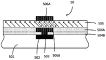
- Figure 5 is a cross-sectional view showing the crossbar structure of a ferroelectric memory cell of a ferroelectric memory integrated circuit in accordance with a fifth embodiment of the present invention.
- Figure 6 is a cross-sectional view showing the structure of a 1T1R structure of a ferroelectric memory cell of a ferroelectric memory integrated circuit in accordance with a sixth embodiment of the present invention.
- Fig. 7 is a circuit connection diagram of a crossbar structure of a ferroelectric memory cell according to the embodiment shown in Fig. 1, Fig. 3 or Fig. 5.
- Figure 8 is a view showing a configuration operation of writing storage information "1" to a certain ferroelectric memory cell of the ferroelectric memory array of the ferroelectric memory integrated circuit of the embodiment shown in Figure 1, Figure 3 or Figure 5.
- Figure 9 is a view showing a configuration operation of writing information "0" to a ferroelectric memory cell of the ferroelectric memory array of the ferroelectric memory integrated circuit of the embodiment shown in Figure 1, Figure 3 or Figure 5.
- Figure 10 is a view showing a configuration operation of reading information from a ferroelectric memory cell of a ferroelectric memory array of the ferroelectric memory integrated circuit of the embodiment shown in Figure 1, Figure 3 or Figure 5.
- Figure 11 is a circuit connection diagram of a 1T1R structure of a ferroelectric memory cell in accordance with the embodiment shown in Figures 2, 4 or 6.
- Figure 12 is a diagram showing the configuration operation of writing storage information "1" to a certain ferroelectric memory cell of the ferroelectric memory array of the ferroelectric memory integrated circuit of the embodiment shown in Figure 2, Figure 4 or Figure 6.
- Figure 13 is a view showing the configuration operation of writing information "0" to a certain ferroelectric memory cell of the ferroelectric memory array of the ferroelectric memory integrated circuit of the embodiment shown in Figure 2, Figure 4 or Figure 6.
- Figure 14 is a diagram showing the operation of reading information from a ferroelectric memory cell of a ferroelectric memory array of the ferroelectric memory integrated circuit of the embodiment shown in Figure 2, Figure 4 or Figure 6.
- 15 is an SEM image of a sample of a ferroelectric memory array of a ferroelectric memory cell having a crossbar structure in accordance with an embodiment of the present invention.
- Figure 16 is a diagram showing the I-V characteristics of the ferroelectric memory cell of the ferroelectric memory array in accordance with the embodiment of Figure 15, wherein the ordinate is in logarithmic form and the scan voltage ranges from 0 to +10V.
- Figure 17 is a diagram showing the I-V characteristics of the ferroelectric memory cell of the ferroelectric memory array in accordance with the embodiment of Figure 15, wherein the scan voltage ranges from -10V to +10V.
- Figure 18 is a flow chart showing a method of fabricating a ferroelectric memory integrated circuit corresponding to the first embodiment shown in Figure 1.
- Figure 19 is a flow chart showing a method of fabricating a ferroelectric memory integrated circuit corresponding to the second embodiment shown in Figure 2.
- Figure 20 is a flow chart showing a method of fabricating a ferroelectric memory integrated circuit corresponding to the third embodiment shown in Figure 3.
- Figure 21 is a flow chart showing a method of fabricating a ferroelectric memory integrated circuit corresponding to the fourth embodiment shown in Figure 4.
- Figure 22 is a flow chart showing a method of fabricating a ferroelectric memory integrated circuit corresponding to the fifth embodiment shown in Figure 5.
- Figure 23 is a flow chart showing a method of fabricating a ferroelectric memory integrated circuit corresponding to the sixth embodiment shown in Figure 6.
- the domain direction or the polarization direction is exemplarily given for clarity of description, but it should be understood that the domain direction or polarization direction of the ferroelectric memory is not limited to the embodiment as shown in the figure. The direction of the out.
- the ferroelectric single crystal refers to a single crystal structure or a single crystal-like structure in which a "grain boundary" of a polycrystalline structure is not present internally; the memory cell of the memory cell array formed thereon is also a single crystal structure, and the size of the memory cell is not limit.
- the ferroelectric single crystal may be a ferroelectric single crystal thin film layer or a ferroelectric single crystal substrate, and the ferroelectric single crystal thin film layer may be a single crystal thin film formed by epitaxial single crystal growth, or separated from the ferroelectric single crystal substrate or The formed film layer is cut.
- the ferroelectric memory integrated circuit includes a ferroelectric memory array, and the plurality of ferroelectric memory cells in the ferroelectric memory array are arranged in rows and columns; thus, by reading and writing circuits, corresponding rows are corresponding columns
- the ferroelectric memory cell can be selected for a corresponding write or read operation. It should be noted that the specific number, arrangement, and the like of the ferroelectric memory cells in the ferroelectric memory array are not limited.
- the ferroelectric memory integrated circuit 10 of this embodiment includes a ferroelectric single crystal substrate 101 which is formed by etching on a ferroelectric single crystal substrate 101 and formed at the left and right ends of each memory cell 102.
- the first electrode 103A and the second electrode 103B; in one embodiment, the ferroelectric memory integrated circuit 10 further includes an insulating layer 105 over the above structure of the ferroelectric single crystal substrate 101 and overlying the insulating layer 105 Silicon based read and write circuit 106, plate line 104 and bit line 108.
- the plate line 104 is also referred to as a "Plate Line” and may also be a drive line.
- the bit line 108 may pass through the contact hole 107 formed in the insulating layer 105 and the corresponding column of the memory unit 102.
- the second electrodes 103B are connected.
- the ferroelectric memory integrated circuit 20 includes a ferroelectric single crystal substrate 201.
- the memory cell array 202 is etched on the ferroelectric single crystal substrate 201, and the first electrode 203A and the left and right ends of the memory cell array 202 are respectively formed.
- the second electrode 203B is formed in one embodiment, the ferroelectric memory integrated circuit 20 further includes an insulating layer 205 and a silicon-based read/write circuit 206 and a transistor array 209 disposed on the insulating layer 205.
- the transistor array 209 is formed on the silicon-based read/write circuit 206.
- each transistor of the transistor array 209 is used to control the gating of the corresponding memory cell, and is therefore also referred to as a switching transistor; each transistor of the transistor array 209 has a gate 209C, a source 209A and a drain 209B, The on-off between the source 209A and the drain 209B is controlled by controlling the switching control signal applied to the gate 209C.
- the ferroelectric memory integrated circuit 20 further includes a plate line 204, a bit line 211, and a word line 210.
- the plate line 204 is also referred to as a "Plate Line" and may also be a drive line.
- the bit line 208 may pass through the contact hole 207 formed in the insulating layer 205 and the corresponding column of the memory unit 202.
- the second electrode 203B is connected, and the bit line 208 is also connected to, for example, the drain 209B of the transistor of the corresponding column.
- the ferroelectric single crystal substrate 101 or 201 may be, but not limited to, a ferroelectric single crystal epitaxial wafer, for example, on a conventional single crystal substrate (e.g., 100 orientation of a SrTiO 3 single crystal substrate).
- a ferroelectric thin film (such as BiFeO 3 , etc.) is formed.
- the ferroelectric memory integrated circuit 30 may include a silicon-based read/write circuit 301, an insulating layer 302, a ferroelectric single crystal thin film layer 303, a memory cell array 304 etched on the ferroelectric single crystal thin film 303, The first electrode 305A and the second electrode 305B, the plate line 306, and the bit line 308 formed at both ends of the memory cell array 304; wherein the silicon-based read/write circuit 301 can be formed, for example, by a single crystal silicon substrate or the like, and the insulating layer 302
- the ferroelectric single crystal thin film layer 303 is mainly used to form the memory cell array 304.
- the memory cells of the memory cell array 304 pass through the contact holes 307 in the insulating layer 302.
- the bit line 308 formed over the silicon-based read/write circuit 301 is
- the ferroelectric memory integrated circuit 40 may include a silicon-based read/write circuit 401 and a transistor array 409.
- the silicon-based read/write circuit 401 may be formed, for example, by a single crystal silicon substrate or the like, and the transistor array 409 may also pass through a single crystal.
- the ferroelectric memory integrated circuit 40 may further include an insulating layer 402, a ferroelectric single crystal thin film layer 403, and a memory cell array 404 formed on the ferroelectric single crystal film 403, on the left and right of the memory cell array 404.
- the first electrode 405A and the second electrode 405B respectively formed at both ends further include a plate line 406, a bit line 411, and a word line 410.
- each transistor in the transistor array 409 is used to gate a memory cell in the memory cell array 404 to which it is connected, having a gate 409C, a source 409A and a drain 409B, controlled by a switch applied on the gate 409C.
- the signal can control the on and off of the electrical connection of the bit line 411 to the corresponding memory cell; the bit line 411 is coupled to the source or drain (eg, source 409A) of the transistor 409 of the corresponding column of ferroelectric memory cells of the ferroelectric memory array, Word line 410 is coupled to gate 409C of transistor 409 of a corresponding column of ferroelectric memory cells of a ferroelectric memory array, such as patterned on gate 409C of transistor 409 of the corresponding column.
- FIG. 5 is a cross-sectional view showing the crossbar structure of a ferroelectric memory cell of a ferroelectric memory integrated circuit in accordance with a fifth embodiment of the present invention.
- the ferroelectric memory integrated circuit 50 can include a silicon-based read/write circuit 501, a bit line 502, and a contact hole 503.
- the bit line 502 and the second electrode 506B can be connected through a conductive connection in the contact hole 503.
- the electrical connection; the ferroelectric memory integrated circuit 50 may further include an insulating layer 504, a ferroelectric single crystal thin film layer 505, and a first electrode 506A over the ferroelectric single crystal thin film layer 505.
- the first electrode 506A may also be a part of the plate line, and the plate line is connected to the plurality of first electrodes 506A of the memory cells of the corresponding row or column of the ferroelectric memory unit, and the first electrode 506A may be substantially opposite to the second electrode 506B.
- the second electrode 506B is specifically formed on the upper and lower sides of the ferroelectric single crystal thin film layer 505, and the second electrode 506B is specifically patterned in the insulating layer 504.
- the insulating layer 504 includes a lower insulating layer 504B and an upper insulating layer. 504A.
- a portion of the ferroelectric single crystal thin film layer 505 between the first electrode 506A and the second electrode 506B constitutes a memory cell of an embodiment of the present invention, thereby enabling an electrical signal to be applied between the first electrode 506A and the second electrode 506B.
- the domain of the partial ferroelectric single crystal thin film layer 505 for forming the memory cell substantially between the first electrode 506A and the second electrode 506B is locally inverted (the other portion of the ferroelectric single crystal thin film layer 505 is not reversed)
- Figure 6 is a cross-sectional view showing the structure of a 1T1R structure of a ferroelectric memory cell of a ferroelectric memory integrated circuit in accordance with a sixth embodiment of the present invention.
- the ferroelectric memory integrated circuit 60 may include a silicon-based read/write circuit 601 and a transistor array 602.
- the silicon-based read/write circuit 601 may be formed, for example, by a single crystal silicon substrate or the like, and the transistor array 609 may also pass through a single crystal.
- a silicon substrate or the like is formed.
- the ferroelectric memory integrated circuit 60 can also include a bit line 604, a word line 603, and a contact hole 605 in the insulating layer, wherein the bit line 604 and the source of the transistor 602 of the corresponding column of ferroelectric memory cells of the ferroelectric memory array or The drains (e.g., source 602A) are connected, and the word lines 603 are coupled to the gate 602C of the transistor 602 of the corresponding column of ferroelectric memory cells of the ferroelectric memory array, for example, patterned on the gate 602C of the corresponding column of transistor 602.
- the bit line 604 can be electrically connected to the second electrode 608B through a conductive connection in the contact hole 605.
- the ferroelectric memory integrated circuit 50 may further include an insulating layer 606, a ferroelectric single crystal thin film layer 607, and a first electrode 608A over the ferroelectric single crystal thin film layer 607.
- the first electrode 608A may also be a part of the plate line, and the plate line is connected to the plurality of first electrodes 608A of the memory cells of the corresponding row or column of the ferroelectric memory unit, and the first electrode 608A may be substantially opposite to the second electrode 608B.
- the second electrode 608B is specifically formed on the upper and lower sides of the ferroelectric single crystal thin film layer 607, and the second electrode 608B is specifically patterned in the insulating layer 606.
- the insulating layer 606 includes a lower insulating layer 606A and an upper insulating layer. 606B.
- a portion of the ferroelectric single crystal film layer 607 between the first electrode 608A and the second electrode 608B constitutes a memory unit of the embodiment of the present invention, and the first electrode 608A can be connected through the memory unit. And a domain wall conductive path of the second electrode 608B substantially in the up and down direction.
- a material usable for the ferroelectric single crystal substrate or the ferroelectric single crystal thin film layer is selected from one or more of the following: lithium tantalate salt LiTaO 3 , lithium niobate LiNbO 3, bismuth iron BiFeO 3; or from one or more of the following: doped with MgO, Mn 2 O 5 or Fe salt of lithium tantalate LiTaO 2 O 3 of 3, lithium niobate LiNbO 3 , barium ferrite BiFeO 3 and so on.
- the doping amount of the lithium niobate LiTaO 3 and the lithium niobate LiNbO 3 doped with MgO, Mn 2 O 5 or Fe 2 O 3 may be 0.1 to 10 mol% (for example, 1 mol% or 4 mol%).
- the polarization direction of the ferroelectric single crystal layer (for example, a ferroelectric single crystal substrate or a ferroelectric single crystal thin film layer) as a storage medium may be limited to There is a component in the direction of the connection between the first electrode and the second electrode, and it can be understood that the polarization direction of the domain of the ferroelectric single crystal layer has a certain angle with the direction of the connection between the first electrode and the second electrode but There is a component in the wiring direction but not perpendicular to the wiring direction.
- the polarization direction of the domain is at an angle to the direction of the line connecting the first electrode and the second electrode in the in-plane (or "lateral" direction but in the direction of the connection.
- the direction has an angle but there is a component in the direction of the connection.
- each of the memory cells formed in the memory cell array of the ferroelectric single crystal substrate or the ferroelectric single crystal thin film layer is a regular bump pattern.
- Forming a convex pattern on the surface of the ferroelectric single crystal substrate by a semiconductor micro/nano processing process, that is, the memory cell is a relatively convex programming formed by patterning on a ferroelectric single crystal substrate or a ferroelectric single crystal thin film layer Bump.
- a memory array pattern can be formed on the surface of the ferroelectric single crystal substrate or the ferroelectric single crystal thin film layer by optical exposure or electron beam etching, and further, the bump storage can be further performed by wet etching or dry etching. unit.
- the bump is at least partially located between the first electrode and the second electrode, since the polarization direction of the domain is substantially non-parallel to the normal direction of the ferroelectric single crystal substrate or the ferroelectric single crystal film layer, at the first
- the ferroelectric single crystal of the at least partially convex portion of the ferroelectric single crystal substantially between the first electrode and the second electrode can be made to be ferroelectric single crystal substrate or ferroelectric with respect to other portions.
- the single crystal thin film layer is partially inverted, and the inverted ferroelectric single crystal can form an electrically conductive domain wall with respect to the remaining unreversed ferroelectric single crystal, thereby establishing domain wall conduction connecting the first electrode and the second electrode. aisle.
- the reading and writing operation of the information stored in the memory cell is to bias the corresponding voltage signal to the first electrode and the second electrode through the plate line and the bit line.
- the ferroelectric memory cell of the 1T1R structure it is also necessary to bias the corresponding gate control signal through the gate line of the word line to gate the transistor, thereby operating the corresponding ferroelectric memory cell. Storage unit.
- the selected electrode material is resistant to high temperature and has low resistivity
- the material of the first electrode and/or the second electrode may be, but not limited to, one selected from the following materials. Or a plurality of: TiN, Pt, PtSi, NiSi, TiW, Ta, Ti, W, Mo, Al, Cu, Cr or SrRuO 3 , RuO 2 , etc.; in the embodiment of Figures 1-4, except the first electrode and the first
- a third electrode may be disposed corresponding to each of the storage units, and the third electrode is located between the first electrode and the second electrode (for example, disposed on an upper surface of the bump-shaped memory unit), and respectively respectively Both the electrode and the second electrode have a gap.
- the height (h) of the bump of the memory cell may be greater than or equal to 2 nanometers and less than or equal to 5 micrometers, for example, 100 nanometers; the first electrode and the second electrode
- the thickness of one electrode and the second electrode may be greater than or equal to 1 nanometer and less than or equal to 500 nanometers, such as 50 nanometers.
- the insulating layer may comprise an insulating material such as silicon dioxide, aluminum oxide, hafnium oxide or silicon nitride, for example, the insulating layer is a silicon dioxide film.
- the method of preparing the insulating layer may be selected from one of the following methods: chemical vapor deposition, physical vapor deposition, atomic layer deposition, and the like.
- the circuit structure of the silicon-based read/write circuit is not limited, and may include corresponding circuits having various functions required for realizing the operation of the memory, for example, mainly including The current amplifying circuit, the reference circuit, the output comparator, the addressing circuit, and the like are read out.
- the read current signal may be amplified by a certain multiple, and then compared with the reference current to determine the stored logic state. .
- the first electrode and the second electrode are biased with a write voltage in a first direction, and the first direction is a ferroelectric single crystal substrate or a ferroelectric single crystal.
- the polarization direction of the film layer is opposite to the direction of the connection between the first electrode and the second electrode, that is, the first direction is the direction from the first electrode to the second electrode, and the magnitude of the write voltage is at least greater than the correction of the memory cell.
- the coercive voltage causes the polarization of the domain in the memory cell to be completely reversed (relative to the other ferroelectric single crystal substrate or ferroelectric single crystal film layer of the memory cell), as shown in Figure 1-6.
- the dotted arrow in the figure indicates the direction of polarization reversal, which is opposite to the polarization direction in which the ferroelectric single crystal substrate or film is not reversed, so that a conductive domain wall is formed at the interface, and offset writing is performed. After the voltage is removed, the conductive domain wall does not disappear. This process writes the message "1" (ie, the logic state "1").
- the first electrode and the second electrode bias voltage are biased in a second direction opposite to the first direction, and the voltage is at least larger than the memory cell.
- the coercive field voltage, the write voltage in the second direction can cause the domain polarization direction of the memory cell to be all reversed back to the initial state, that is, the initial polarization in the ferroelectric single crystal substrate or the ferroelectric single crystal thin film layer
- the direction is the same, the conductive domain wall formed at the interface disappears, the process is to write "0" information (ie logic state "0");
- the first electrode and the second electrode bias voltage are biased by the read voltage in the first direction, and the read voltage is smaller than the storage cell coercive field voltage.
- the information is read by current, and the read current changes according to the generation or disappearance of the above low-resistance domain wall. By comparing the read current with the reference current circuit, the logic state “0” or “1” can be identified.
- the process is the process of reading information. Since the biased read voltage is small and the polarization direction of the memory cell has been reversed, there is no influence on the polarization state of the memory cell, and non-destructive reading is realized;
- a third electrode may be disposed corresponding to each memory cell; and during a read operation, between the first electrode and the third electrode When the read voltage in the first direction or the read voltage in the first direction is biased between the third electrode and the second electrode, the logic state "0" or "1" is identified by the magnitude of the read current.
- Fig. 7 is a circuit connection diagram showing a crossbar structure of a ferroelectric memory cell according to the embodiment shown in Fig. 1, Fig. 3 or Fig. 5.
- the illustrated ferroelectric memory array includes a plurality of ferroelectric memory cells as shown in Figure 7 arranged in rows and columns, with bit lines BL Arranged in the column direction, the plate line PL (or referred to as a drive line) is arranged in the row direction as an example, and the resistive memory cell of the ferroelectric memory cell is in the vicinity of the intersection point of the bit line BL and the plate line PL in space.
- the bit line BL is connected to the plate line PL.
- the second electrode of the memory cell is connected to the bit line BL0 and the first electrode connection plate line BL0 of the memory cell. Assuming that the address signal bit line BL0 and the board line BL0 are selected and biased corresponding to the read signal or the write signal, a read operation or a write operation can be performed on the corresponding memory cell at the intersection of the bit line BL0 and the board line BL0. Other unselected memory locations will not be read or written.
- each ferroelectric memory cell is mainly formed by one memory cell in the memory cell array, one end of which is connected to the plate line PL and the other end is connected to the bit line BL.
- the bit line BL can be connected to the current comparator SA input by the reference current Ref so that the logic state currently stored by the memory cell can be read.
- a current amplifier is required on the current comparator to amplify the current read on the bit line.
- the memory cell of the ferroelectric memory cell is a resistive ferroelectric memory cell because the ferroelectric memory integrated circuit provided can write data in a bias voltage manner and read data in a manner of reading current.
- the magnitude of the read current reflects the resistance of the memory cell to a certain extent.
- the write operation of the memory cell reflects the change of the resistance of the memory cell to some extent. Therefore, in the embodiment of the present invention, the storage unit can be represented by R.
- the crossbar structure of the embodiment shown in Fig. 7 corresponds to an OT1R structure (T denotes a transistor for strobe).
- FIG. 8-10 illustrate a ferroelectric memory array of a ferroelectric memory integrated circuit according to an embodiment of the present invention, in which the ferroelectric memory array is a 1024 ⁇ 8 memory array, that is, 1024 ⁇ 8 are arranged in rows and columns.
- the plate line PL is connected to the first electrode of the memory cell of the corresponding row of ferroelectric memory cells
- the bit line BL is connected to the second electrode of the memory cell of the corresponding column of ferroelectric memory cells.
- the target memory cell is selected for read and write operations by the board line PL and the bit line BL.
- the memory cell read current has a switching characteristic, that is, a large on-state current is read under the condition that the first electrode and the second electrode bias voltage bias the voltage in the first direction and the conductive domain wall exists.
- the output information is "1", that is, corresponding to the low resistance state; other conditions such as the disappearance of the domain wall, the off-state current is read, and the readout information is "0", that is, the high resistance state is corresponding.
- the memory cell since the memory cell is formed using the ferroelectric single crystal layer, it has a characteristic of a ratio of an on-state current to an off-state current (i.e., a switching ratio) (e.g., an on state).
- the ratio of the current to the off-state current can be greater than 10 6 ), so that during the read operation or the write operation, crosstalk is not generated to the adjacent memory cells of the selected memory cell, and the leakage power consumption is also small. Therefore, each ferroelectric memory cell
- the transistor for strobing can be omitted directly to form a ferroelectric memory cell of a crossbar structure.
- ferroelectric memory cell having a crossbar structure eliminates the need for transistors, the ferroelectric memory cell and the ferroelectric memory array are simple in construction, low in cost, and the peripheral read and write circuits are correspondingly simple.
- the on-state read current can reach, for example, 10 -7 A or more, and the data readability is good.
- FIG. 8 is a view showing a configuration operation of writing storage information "1" to a certain ferroelectric memory cell of the ferroelectric memory array of the ferroelectric memory integrated circuit of the embodiment shown in Figure 1, Figure 3 or Figure 5.
- the ferroelectric memory cell at address (1022, 6) is selected to perform the operation of writing the storage information "1"; first, the read enable terminal RE is configured to a low level, thereby blocking the bit line and The current comparison circuit is connected; then, the plate line PL1022 is configured to a high voltage V write , the V write value is greater than the coercive field voltage of the memory cell, and the other plate lines are left floating or configured to be a half level V cc /2 while Bit line BL6 is configured to be grounded, and other bit lines are left floating or configured as a half-level V cc /2.
- a write signal V write to the memory cell is biased in the ferroelectric memory cell address (1022,6) of the memory cell ferroelectric domain inversion occurs, successfully written to the storage
- the drive line PL1022 and the bit line BL6 are left floating or arranged at a half level V cc /2.
- FIG. 9 is a view showing a configuration operation of writing information "0" to a ferroelectric memory cell of the ferroelectric memory array of the ferroelectric memory integrated circuit of the embodiment shown in Figure 1, Figure 3 or Figure 5.
- the ferroelectric memory cell having the address (1022, 6) is selected to perform the operation of writing the storage information "0"; first, the read enable terminal RE is configured to be low, thereby blocking the bit line and The current comparison circuit is connected; then, the bit line BL6 is configured to a high voltage V write , the V write value is greater than the coercive field voltage of the memory cell, and the other bit lines are left floating or configured as a half level V cc /2 while The plate line PL1022 is configured to be grounded, and the other plate lines are left floating or configured to be a half level V cc /2.
- a write signal V write to the memory cell is biased in the ferroelectric memory cell address (1022,6), the electrical domain of the memory cell returns to the original direction of polarization, information
- the drive line PL1022 and the bit line BL6 are left floating or arranged at a half level V cc /2.
- FIG. 10 is a view showing a configuration operation of reading information from a ferroelectric memory cell of a ferroelectric memory array of the ferroelectric memory integrated circuit of the embodiment shown in Figure 1, Figure 3 or Figure 5.
- the ferroelectric memory cell at address (1022, 6) is selected for read operation; first, the read enable terminal RE is configured to be high, thereby connecting the bit line BL with the current comparison circuit; PL1022 drive line configured to read voltage V read, V read correction value is less than the coercive field voltage of the memory cell, the floating or other drive line configured to half the high level V cc / 2, at the same time, the bit line BL6 configured to ground, The other bit lines are left floating or configured as a half high level V cc /2.
- the sense current is compared to the reference current by the input current comparator to determine the logic state stored by the ferroelectric memory cell at address (1022, 6).
- the drive line PL1022 and the bit line BL6 are left floating or arranged at a half level V cc /2.
- FIG 11 is a circuit connection diagram of a 1T1R structure of a ferroelectric memory cell in accordance with the embodiment shown in Figure 2, Figure 4 or Figure 6.
- the illustrated ferroelectric memory array includes a plurality of ferroelectric memory cells as shown in Figure 11 arranged in rows and columns, with bit lines BL And the plate line PL (or referred to as a drive line) are arranged in the column direction, the word line WL is arranged in the row direction as an example, the resistive memory cell R of the ferroelectric memory cell and the transistor T are spatially in the bit line BL and the plate line PL
- the bit line BL is connected to the plate line PL in the vicinity of the intersection point.
- the first electrode connection plate line BL0 of the memory cell and the second electrode of the memory cell are connected to the transistor T and further pass.
- the transistor T is connected to the bit line BL0
- the transistor T of the memory cell is connected to the word line WL0.
- the corresponding bit line BL0, the board line BL0, and the word line WL0 are selected and biased corresponding to the read signal or the write signal based on the address signal, the selected memory cell can be read or written, and the other unselected The memory unit does not read or write.
- each ferroelectric memory cell is mainly formed by one memory cell R and one transistor T in the memory cell array, that is, a 1T1R structure is formed, one end of the memory cell is connected to the plate line (PL0), and the other end is connected.
- the gate of the transistor T is connected to the word line (WL0), and the other end of the source and the drain of the transistor T is connected to the bit line (BL0).
- the bit line BL can be connected to the current comparator SA input by the reference current Ref so that the logic state currently stored by the memory cell can be read.
- FIG. 12-14 illustrate a ferroelectric memory array of a ferroelectric memory integrated circuit according to still another embodiment of the present invention, wherein the ferroelectric memory array is a 1024 ⁇ 16 memory array, that is, 1024 ⁇ 16 arranged in rows and columns.
- the plate line PL is connected to the first electrode of the memory cell of the corresponding column of the ferroelectric memory cell
- the bit line BL is connected to the source or the drain of the transistor of the corresponding column of the ferroelectric memory cell
- the word line WL The gate of the transistor of the corresponding column of the ferroelectric memory cell is connected, and the target memory cell can be selected through the plate line PL, the bit line BL and the word line WL, thereby performing read and write operations on the selected target memory cell.
- ferroelectric memory cell of 1T1R structure is used, although the ferroelectric memory cell structurally opposite to the crossbar structure is structurally complex, but it is reduced in the array It has beneficial characteristics in terms of crosstalk and leakage current, and is relatively more suitable for larger ferroelectric memory integrated circuits.
- FIG. 12 is a diagram showing the configuration operation of writing storage information "1" to a certain ferroelectric memory cell of the ferroelectric memory array of the ferroelectric memory integrated circuit of the embodiment shown in Figure 2, Figure 4 or Figure 6.
- FIG. 12 shows an expanded circuit of the ferroelectric memory cell shown in FIG. 11, that is, a ferroelectric memory array. As shown in FIG. 8, the ferroelectric memory cell at address (1022, 14) is selected to be written to store information. 1" operation.
- the read enable terminal RE is configured to be low, thereby blocking the connection of the bit line to the current comparison circuit; then, the configuration plate line PL14 is high voltage V write , and the V write value is greater than the coercive field voltage of the memory cell,
- the other board line PL is left floating or configured as a half-level V cc /2;
- the configuration bit line BL14 is grounded, and the other bit lines BL are left floating or configured as a half-level V cc /2.
- a write signal V write to the memory cell is biased in the ferroelectric memory cell address (1022,14), and the memory cell ferroelectric domain inversion occurs, successfully written to the storage information "1."
- the plate line PL14 and the bit line BL14 are suspended or arranged to be a half-level Vcc/2, and the word line W1022 is also suspended or arranged at a low level.
- FIG. 13 is a view showing the configuration operation of writing information "0" to a certain ferroelectric memory cell of the ferroelectric memory array of the ferroelectric memory integrated circuit of the embodiment shown in Figure 2, Figure 4 or Figure 6.
- the ferroelectric memory cell having the address (1022, 14) is selected to perform the operation of writing the storage information "0".
- the read enable terminal RE is configured to be low, thereby blocking the connection of the bit line to the current comparison circuit; then, the plate line PL14 is configured to be grounded, and the other plate line PL is suspended or configured as a half level V cc / 2; the bit lines BL14 configured for high voltage V write, V write the memory cell is greater than the coercive voltage Ec.
- a write signal V write to the memory cell is biased in the ferroelectric memory cell address (1022,14), the electrical domain of the memory cell returns to the original direction of polarization, information stored successfully written "0.”
- the plate line PL14 and the bit line BL14 are suspended or arranged to be a half-level Vcc/2, and the word line W1022 is also suspended or arranged at a low level.
- Figure 14 is a diagram showing the operation of reading information from a ferroelectric memory cell of a ferroelectric memory array of the ferroelectric memory integrated circuit of the embodiment shown in Figure 2, Figure 4 or Figure 6.
- the ferroelectric memory cell at address (1022, 14) is selected for read operation.
- the configuration read enable terminal RE is high, so as to connect the bit line BL and the current comparator circuit; then, the plate lines PL14 configured as a voltage V read, V read memory cell is less than the coercive field voltage, the other plate
- the line PL is left floating or configured as a half-level V cc /2; the bit line BL14 is configured to be grounded, and the other bit lines BL are left floating or configured as a half-level V cc /2.
- the sense current is compared to the reference current by the current comparator to determine the logic state stored by the ferroelectric memory cell at address (1022, 6).
- the drive line PL14 and the bit line BL14 are left floating or arranged to be a half-level V cc /2, and the word line W1022 is also left floating or configured as a low level.
- Figure 15 is a SEM image of a sample of a ferroelectric memory array of a ferroelectric memory cell having a crossbar structure in accordance with an embodiment of the present invention.
- a LiNbO 3 ferroelectric single crystal substrate doped with MgO mol of 5% was used, the height of each memory cell was about 70 nm, and the thickness of the first electrode and the second electrode was about 30.
- Nano having a width of about 100 nm, the first electrode is connected to the plate line PL, and a layer of about 200 nm thick silicon dioxide insulating layer is deposited between the plate line PL and the bit line BL, and the bit line BL is passed through the silicon dioxide insulating layer.
- the contact hole is connected to the second electrode and is tested by being led out from the bit line BL and the plate line PL.
- Figure 16 is an I-V test diagram of 12 memory cells randomly sampled in the sample of the embodiment of Figure 15, i.e., an I-V curve of a ferroelectric memory cell; wherein the ordinate is in logarithmic form.
- the voltage is forward-biased for scanning.
- the scan voltage ranges from 0 to 10V. Since the memory cell does not form a domain-wall conductive channel at the beginning, the current after the bias voltage is small, the memory cell is in a high-resistance state, and the scan voltage increases.
- the memory cell After exceeding the coercive field voltage of the memory cell, the memory cell forms a domain wall conductive path, and the current suddenly increases at a bias voltage of, for example, 6-7V, and the current suddenly increases by nearly 4 orders of magnitude; when the scan voltage is reversed from 10V At 0V, the memory cell is in a low resistance state and the current is large.
- This I-V scanning process completes the information writing process of the memory cell, that is, the formation process of the domain wall conductive channel.
- the ferroelectric memory array of the embodiment of the present invention has a crossbar structure, and the ratio of the on-state current to the off-state current of the ferroelectric memory cell measured in the array can be greater than 10 4 , and the ferroelectric memory The crosstalk in the array is small.
- Figure 17 is an IV test diagram of 12 memory cells randomly sampled in the sample of the embodiment of Figure 15, scanning from -10V to +10V, and then scanning from +10V to -10V, as can be seen from Figure 15
- the memory cell of the example has obvious switching characteristics. When the scanning voltage is taken in the negative direction, the stored cell cannot be turned on, that is, the low resistance state cannot be read. It can be seen that the memory cell has a unidirectional conduction characteristic. For example, after a low resistance state in which a domain wall conductive path is formed by forward programming, if the memory cell is biased with a negative voltage, the low resistance state cannot be read. The memory cell can be rendered in a low resistance state only if the same forward voltage is used to bias the memory cell.
- the ferroelectric memory cell of the crossbar structure of the embodiment of the present invention when applied to a ferroelectric memory array, the unidirectional conduction characteristic of the memory cell naturally contributes to avoiding the surrounding ferroelectric memory cells and surrounding ferroelectrics in the array.
- Current crosstalk between memory cells As shown in the example of FIG. 10, when the high resistance state of the memory cell R H is read, since the surrounding memory cells R L1 , R L2 , and R L3 are all in a low resistance state, even if the current tends to pass the b path (see FIG. 10).
- the negative resistance is programmed to form a low resistance state with domain wall conduction paths, if the memory cell is biased with a positive voltage, the low resistance state cannot be read, only if the same negative voltage is used. In the case of biasing the memory cell, the memory cell can be turned on in a low resistance state.
- FIG. 18 is a flow chart showing a method of fabricating the ferroelectric memory integrated circuit of the first embodiment shown in FIG. Referring to FIG. 1 and FIG. 18, first, in step S181, a ferroelectric single crystal substrate or a ferroelectric thin film is provided.
- the ferroelectric material may be selected from one or more of the following materials: lithium tantalate salt LiTaO 3 , tannic acid Lithium salt LiNbO 3 , BiFeO 3 or lithium niobate LiTaO 3 doped with MgO, Mn 2 O 5 or Fe 2 O 3 , lithium niobate LiNbO 3 , BiFeO 3 ferrite, and the like.
- a memory cell array is formed.
- the array pattern can be formed by optical exposure, electron beam exposure, etc., and then the array pattern can be transferred to the surface of the ferroelectric single crystal substrate or the ferroelectric film by wet etching or dry etching. Thereby a bump array, that is to say a memory cell array, is formed.
- the first and second electrodes and the plate line are formed.
- the electrode pattern is formed by optical exposure, electron beam exposure, or the like, and then the electrode film material is grown, and the electrode pattern is transferred to the memory cell array by a process such as lift-off; or a long electrode film material is passed through Optical exposure, electron beam exposure and the like form a pattern of electrode patterns, and the electrode patterns are transferred to the memory array by etching methods such as wet or dry etching.
- the first and second electrodes and the plate line (or plate line) PL may be made of the same material and may be formed simultaneously.
- an insulating layer is formed.
- an insulating layer is grown on the ferroelectric single crystal substrate, and the insulating layer material may be silicon dioxide (SiO 2 ), aluminum oxide (Al 2 O 3 ), hafnium oxide (HfO 2 ), An insulating material such as magnesium oxide (MgO), however, it should be understood herein that the insulating layer material is not limited to the insulating material type exemplified above.
- the method of growing the insulating layer material may be, but not limited to, physical vapor deposition, chemical vapor deposition, atomic layer deposition, molecular beam epitaxy, laser pulse deposition, and the like.
- the silicon thin film material is bonded or grown.
- a silicon thin film layer is formed over the insulating layer by an SOI process.
- the process of bonding the silicon thin film material includes ion implantation of the Si/SiO 2 sheet, bonding it to the ferroelectric single wafer, Strip the remaining silicon, chemical mechanical polishing and other steps.
- a silicon thin film material may also be formed over the insulating layer by an epitaxial growth method. It should be noted that the bonded or grown silicon material used above is only one example of a silicon-based material, and it will be understood that the silicon-based material may also be various semiconductors suitable for large-scale preparation of peripheral circuits of a memory.
- Materials are suitable for use in large scale integrated circuit processes to fabricate semiconductor materials including devices such as MOS transistors, such as GaAs, SiC, InP, etc., and, as advances in semiconductor material technology, various types of memory suitable for preparing memories may emerge. New semiconductor materials for peripheral circuits.
- a contact hole is formed in the insulating layer.
- the pattern of the contact hole is formed by optical exposure, electron beam exposure, or the like, and the contact hole pattern is transferred to the insulating layer by wet or dry etching (reactive ion etching), thereby being the upper layer.
- the circuit formed in the silicon film and the memory cell formed in the lower layer provide interconnection channels.
- a bit line and a read/write circuit are formed.
- the electrode pattern is transferred to the ferroelectric memory array by forming a pattern of the electrode pattern, the material of the growth electrode film, peeling, or the like by optical exposure, electron beam exposure, or the like; or a long electrode
- the film material is formed into a pattern by optical exposure, electron beam exposure, etc., and the electrode pattern is transferred to the ferroelectric memory array by wet or dry etching, and the formed bit lines are passed through the contact holes and the corresponding column memory cells. connection.
- the read/write circuit can be prepared through a standard CMOS process to form a silicon-based read/write circuit; the read/write circuit can include, but is not limited to, a read current amplifying circuit, a reference current output circuit, an output current comparator, and an addressing circuit.
- FIG. 19 is a flow chart showing a method of fabricating a ferroelectric memory integrated circuit corresponding to the second embodiment shown in FIG. 2 and FIG. 19, the preparation method shown in FIG. 19 is substantially similar to the preparation method illustrated in FIG. 18.
- the main difference in the preparation method shown in FIG. 19 is that it further includes step S196 in the silicon-based film layer.
- Forming a transistor T thereon that is, forming an array of transistors T on the silicon-based thin film layer before forming the read/write circuit and the bit line; specifically, forming a transistor having a voltage gate-controlled switch on the silicon thin film formed on step S195
- the array has one end of the source and the drain of each transistor electrically connected to the bit line and the other end electrically connected to one end of the lower memory cell.
- Step S191, step S192, step S193, step S194, step S195, step S197, step S198 in the preparation method shown in Fig. 19 may be combined with step S181, step S182, step S183, and step in the preparation method shown in Fig. 18.
- S184, step S185, step S186, and step S187 are respectively the same or similar, and a description thereof will be omitted herein.
- Figure 20 is a flow chart showing a method of fabricating a ferroelectric memory integrated circuit corresponding to the third embodiment shown in Figure 3. As shown in Fig. 20 and Fig. 3, a silicon single crystal wafer is used as a silicon-based substrate in this embodiment to form a peripheral read/write circuit or the like.
- step S201 a silicon single wafer is provided, that is, a single crystal silicon substrate is provided.
- a bit line and a silicon-based read/write circuit are formed on a silicon single wafer by using, for example, a standard CMOS process, wherein the silicon-based read/write circuit includes but is not limited to a read current amplifying circuit, a reference current output circuit, and an output current comparison. And addressing circuits, etc.
- an insulating layer is formed.
- an insulating layer may be grown on the silicon-based read/write circuit and the bit line, and the insulating layer material may be selected from silicon dioxide (SiO 2 ), aluminum oxide (Al 2 O 3 ), and antimony oxide ( Insulating materials such as HfO 2 ) and magnesium oxide (MgO), and methods for growing the insulating material include, but are not limited to, physical vapor deposition, chemical vapor deposition, atomic layer deposition, molecular beam epitaxy, laser pulse deposition, and the like.
- a ferroelectric single crystal thin film layer is bonded or grown on the insulating layer.
- the ferroelectric single crystal thin film layer used as the ferroelectric single crystal layer is formed by bonding over the insulating layer by an SOI process; specifically, bonding to form a ferroelectric single crystal thin film layer includes: The surface of the electric single wafer is implanted with ions (H ions or He ions), the ferroelectric single crystal is bonded to the insulating layer of the silicon single wafer, and the ferroelectric single crystal thin film layer bonded to the insulating layer is peeled off, and finally the chemical is performed. Mechanical polishing, etc.
- a ferroelectric single crystal thin film layer serving as a ferroelectric single crystal layer is grown over the insulating layer by an epitaxial growth method.
- a memory cell array is formed on the surface of the ferroelectric single crystal thin film layer.
- the array pattern can be formed by optical exposure, electron beam exposure, or the like, and then the array pattern can be transferred to the surface of the ferroelectric single crystal substrate or the ferroelectric thin film by wet etching or dry etching, thereby forming a convex shape.
- a block array that is, a memory cell array.
- a contact hole is formed.
- the pattern of the contact hole is formed by optical exposure, electron beam exposure, etc., and the contact hole pattern is transferred to the device by wet or dry (reactive ion) etching to provide mutual memory between the upper memory cell and the lower silicon film circuit.
- the pattern of the contact hole is formed by optical exposure, electron beam exposure, etc., and the contact hole pattern is transferred to the insulating layer by wet or dry etching (reactive ion etching), thereby An interconnection channel is provided for the memory cell formed by the upper layer and the bit line BL formed on the underlying silicon single wafer.
- the first and second electrodes and the plate line are formed.
- the engraved electrode pattern is formed by optical exposure, electron beam exposure, or the like, and then the electrode film material is grown, and the electrode pattern is transferred to the memory cell array by a process such as peeling; or a long electrode film material is passed through
- Optical exposure, electron beam exposure and the like form a pattern of electrode patterns, and the electrode patterns are transferred to the memory array by etching methods such as wet or dry etching.
- the first and second electrodes and the plate line (or plate line) PL may be of the same material and may be formed simultaneously, wherein one of the first and second electrodes passes through the contact hole and the silicon single Bit lines on the wafer are connected.
- FIG. 21 is a flow chart showing a method of fabricating the ferroelectric memory integrated circuit of the fourth embodiment shown in FIG. 4 and FIG. 21, the preparation method shown in FIG. 21 is substantially similar to the preparation method illustrated in FIG. 20, and the main difference in the preparation method shown in FIG. 19 is that it further includes step S212 on the silicon single wafer.
- Step S211, step S213, step S214, step S215, step S216, step S217, step S218 in the preparation method shown in FIG. 21 may be combined with step S201, step S203, step S204, and step in the preparation method shown in FIG. S205, step S206, and step S207 are the same or similar, respectively, and a description thereof will be omitted herein.
- FIGS. 22 and 23 The fabrication method illustrated in Figures 18-22 above illustrates the basic fabrication process of an in-plane ferroelectric memory integrated circuit.
- the basic preparation process of the out-of-plane ferroelectric memory integrated circuit will be exemplified below based on FIGS. 22 and 23.
- Figure 22 is a flow chart showing a method of fabricating a ferroelectric memory integrated circuit corresponding to the fifth embodiment shown in Figure 5. Referring to Figures 5 and 22, first,
- step S221 a silicon single wafer is provided, that is, a single crystal silicon substrate is provided.
- a bit line, a silicon-based read/write circuit is formed on a silicon single wafer by, for example, a standard CMOS process, and a contact hole 503 is formed in the insulating layer 504A, wherein the silicon-based read/write circuit includes but is not limited to reading A current amplifying circuit, a reference current output circuit, an output current comparator, an addressing circuit, and the like.
- step S223 an insulating layer such as 504B is deposited.
- This step is the same as or similar to step S203 of the example shown in FIG.
- the second 506B is electrically connected to the corresponding bit line 502 through the contact hole 503.
- step S224 a ferroelectric single crystal thin film layer is bonded or grown on the insulating layer. This step is the same as or similar to step S204 of the example shown in Fig. 20.
- a first electrode (plate line) is formed on the polished surface of the ferroelectric single crystal thin film layer, that is, the first electrode and the plate line are integrally formed.
- a portion of the ferroelectric single crystal thin film layer between the first electrode 506A and the second electrode 506B constitutes a memory cell.
- Figure 23 is a flow chart showing the method of fabricating the ferroelectric memory integrated circuit of the sixth embodiment shown in Figure 6. 6 and FIG. 23, the preparation method shown in FIG. 23 is substantially similar to the preparation method illustrated in FIG. 22, and the main difference in the preparation method shown in FIG. 23 is that, in step S232, it is also formed on a silicon single wafer.
- Step S231, step S233, step S234, and step S235 in the preparation method shown in FIG. 23 may be the same as or similar to step S221, step S223, step S224, and step S225 in the preparation method shown in FIG. 22, and are omitted here. A description of them.
- ferroelectric memory integrated circuits of the embodiments shown in Figs. 1-6 are basically formed, respectively.
- the method for fabricating the ferroelectric memory integrated circuit of the embodiment of the present invention has fewer process steps, is not complicated in the preparation process, and is compatible with the CMOS process, compared to the conventional method of fabricating the FRAM of the ferroelectric capacitor structure.
Landscapes
- Engineering & Computer Science (AREA)
- Computer Hardware Design (AREA)
- Power Engineering (AREA)
- Semiconductor Memories (AREA)
- Non-Volatile Memory (AREA)
Abstract
本发明属于铁电存储技术领域,本发明提供的铁电存储集成电路,包括:铁电存储器阵列,其具有在铁电单晶层上形成的存储单元阵列;其中,所述铁电存储器阵列的每个铁电存储器单元主要由存储单元阵列中的一个存储单元形成、或者主要由存储单元阵列中的一个存储单元以及该存储单元电连接的形成于所述硅基读写电路的硅基上的一个晶体管形成。
Description
本发明属于铁电存储技术领域,涉及基于电畴壁导电的铁电存储器阵列、铁电存储集成电路及其操作方法和制备方法。尤其涉及交叉棒(Crossbar)结构和一个开关晶体管和一个铁电存储器单元(1T1R)结构的铁电存储集成电路设计及其制造方法。
传统的铁电存储器是利用铁电材料能够保持极化状态来非挥发性地存储信息。当对铁电电容器(C)施加一个足够大的电压时,铁电电容器的极化方向与电压方向一致,撤销电压后,铁电电容器的极化方向保持不变;当对电容器施加反向足够大电压时,电容器的极化方向反转,撤销电压后,其极化方向保持不变。这样,根据铁电电容器的极化方向不同存储布尔逻辑量“1”或者“0”。
此类铁电电容器具有高剩余极化、良好的矫顽场、高抗疲劳性和低漏电流等优点,早在20世纪50年代已开始用于铁电存储集成电路,参见1959年公布的J.R.Anderson等的美国专利US2876,436。此后,铁电存储技术领域主要致力于对存储单元结构和读写电路的改善,例如,1989年公布的S.Sheffield Eaton,Jr等的美国专利US4873,664,1989年公布的Kenneth J.Mobely等的美国专利US4888,733,1996年公布的L.D.McMillan等的美国专利US5523,964,1998年公布的D.R.Wilson等的美国专利US5572,459,2010年公布的X.H.Du等的美国专利US7652,909B2,它们涉及2T2C、1T1C、参考电路和寻址电路等。但是,在读电路原理上大体是相同的,主要是读取铁电电容器C中的电荷。
然而,随着铁电电容器C的尺寸的逐年减小,可读取的电荷量也在减少,这对电荷检测电路的要求很高,进而增加了电路的读写时间和复杂度,不利于集成度的提高。并且,每次读取都会破坏性的读出电容器中的电荷量,需要重新写入电荷,增加了电路的读写时间。
1998年公布的J.Moon等的美国专利US5744,374中,采用了金属-铁电-绝缘-半导体场效应晶体管结构(MFIS FET),此结构简单,只 有一个晶体管T,并且与当前的CMOS工艺完全兼容,可以简化读写电路,并且,非破坏性的读取信息。但是,对栅极上的铁电单晶薄膜层及其界面质量要求非常高,这非常不利于尺寸的减小和成品率的提高。
近年来,铁电材料中的畴壁导电引起了学术界的广泛兴趣(例如参见Seidel J,Martin L W,He Q,et al.Conduction at domain walls in oxide multiferroics.Nature materials,2009,8(3):229.)。本申请的发明人已经提出了基于畴壁导电的铁电存储器件(参见中国专利申请号CN201510036526.X、CN201510036586.1、CN201610098138.9和美国专利公开号US9685,216B2的专利)。
发明内容
按照本发明的第一方面,提供一种铁电存储集成电路,包括:
铁电存储器阵列,其具有在铁电单晶层上形成的存储单元阵列;和
硅基读写电路;
其中,所述存储单元阵列中的每个存储单元相应地设置有第一电极和第二电极,所述铁电单晶层的电畴的极化方向基本不平行所述铁电单晶层的法线方向,在所述第一电极和第二电极之间施加电信号时,能够使大致位于所述第一电极和第二电极之间的用于形成所述存储单元的铁电单晶层的电畴发生反转,从而能够建立连接所述第一电极和第二电极的畴壁导电通道;
其中,所述铁电存储器阵列的每个铁电存储器单元主要由存储单元阵列中的一个存储单元形成、或者主要由存储单元阵列中的一个存储单元以及该存储单元电连接的形成于所述硅基读写电路的硅基上的一个晶体管形成。
按照本发明的第二方面,提供一种铁电存储器阵列,其中,所述铁电存储器阵列包括在铁电单晶层上形成的存储单元阵列;
其中,所述存储单元阵列中的每个存储单元相应地设置有第一电极和第二电极,所述铁电单晶层的电畴的极化方向基本不平行所述铁电单晶层的法线方向,在所述第一电极和第二电极之间施加电信号时,能够使大致位于所述第一电极和第二电极之间的用于形成所述存储单 元的铁电单晶层的电畴发生反转,从而能够建立连接所述第一电极和第二电极的畴壁导电通道;
其中,所述铁电存储器阵列的每个铁电存储器单元主要由存储单元阵列中的一个存储单元形成。
按照本发明的第三方面,提供一种上述铁电存储集成电路的操作方法,其中,包括:
写入存储信息“1”的步骤:在所述第一电极和第二电极之间施加第一方向的写信号,使能至少部分的所述存储单元的电畴反转,从而建立所述畴壁导电通道;和
读存储信息的步骤:在所述第一电极和第二电极之间施加所述第一方向的读信号,所述读信号的电压大小小于所述存储单元的矫顽场电压。
按照本发明的第四方面,提供一种上述铁电存储集成电路的制备方法,其中,包括步骤:
提供用作铁电单晶层的铁电单晶基片;
在所述铁电单晶基片上构图形成所述存储单元阵列;
在所述铁电单晶基片之上构图形成所述第一电极和第二电极、以及与所述第一电极/第二电极连接的板线;
在所述铁电单晶基片之上生长绝缘层;
通过SOI工艺或外延生长方法在所述绝缘层的上方形成硅基薄膜层;和
在所述硅基薄膜层上形成所述硅基读写电路和位线。
按照本发明的第五方面,提供一种上述铁电存储集成电路的制备方法,其中,包括步骤:
提供单晶硅衬底;
在所述单晶硅衬底上形成所述硅基读写电路和位线;
在所述硅基读写电路和位线之上生长绝缘层;
通过SOI工艺或外延生长方法在所述绝缘层的上方形成用作铁电单晶层的铁电单晶薄膜层;
在所述铁电单晶薄膜层上构图形成所述存储单元阵列;和
在所述铁电单晶薄膜层之上构图形成所述第一电极和第二电极、以及与所述第一电极/第二电极连接的板线。
按照本发明的第六方面,提供一种上述铁电存储集成电路的制备方法,其中,包括步骤:
提供单晶硅衬底;
在所述单晶硅衬底上形成所述硅基读写电路和位线;
在所述硅基读写电路和位线之上生长绝缘层;
在所述绝缘层中形成第一电极;
通过SOI工艺或外延生长方法在所述绝缘层的上方形成用作铁电单晶层的铁电单晶薄膜层;和
在所述铁电单晶薄膜层之上构图形成与所述第一电极基本上下对齐的所述第二电极以及与所述第二电极连接的板线。
根据以下描述和附图本发明的以上特征和操作将变得更加显而易见。
从结合附图的以下详细说明中,将会使本发明的上述和其他目的及优点更加完整清楚,其中,相同或相似的要素采用相同的标号表示。
图1是按照本发明第一实施例的铁电存储集成电路的铁电存储器单元的交叉棒结构截面示意图。
图2是按照本发明第二实施例的铁电存储集成电路的铁电存储器单元的1T1R结构截面示意图。
图3是按照本发明第三实施例的铁电存储集成电路的铁电存储器单元的交叉棒结构截面示意图。
图4是按照本发明第四实施例的铁电存储集成电路的铁电存储器单元的1T1R结构截面示意图。
图5是按照本发明第五实施例的铁电存储集成电路的铁电存储器单元的交叉棒结构截面示意图。
图6是按照本发明第六实施例的铁电存储集成电路的铁电存储器单元的1T1R结构截面示意图。
图7是按照图1、图3或图5所示实施例的铁电存储器单元的交叉棒结构的电路连接图。
图8示意向图1、图3或图5所示实施例的铁电存储集成电路的铁电存储器阵列的某一铁电存储器单元写入存储信息“1”的配置操作图。
图9示意向图1、图3或图5所示实施例的铁电存储集成电路的铁电存储器阵列的某一铁电存储器单元写入信息“0”的配置操作图。
图10示意从图1、图3或图5所示实施例的铁电存储集成电路的铁电存储器阵列的某一铁电存储器单元读取信息的配置操作图。
图11是按照图2、图4或图6所示实施例的铁电存储器单元的1T1R结构的电路连接图。
图12示意向图2、图4或图6所示实施例的铁电存储集成电路的铁电存储器阵列的某一铁电存储器单元写入存储信息“1”的配置操作图。
图13示意向图2、图4或图6所示实施例的铁电存储集成电路的铁电存储器阵列的某一铁电存储器单元写入信息“0”的配置操作图。
图14示意从图2、图4或图6所示实施例的铁电存储集成电路的铁电存储器阵列的某一铁电存储器单元读取信息的配置操作图。
图15是按照本发明一实施例的具有交叉棒结构的铁电存储器单元的铁电存储器阵列的样品的SEM图。
图16是按照图15所示实施例的铁电存储器阵列的铁电存储器单元的I-V特性示意图,其中,纵坐标取对数形式,扫描电压范围为0-+10V。
图17是按照图15所示实施例的铁电存储器阵列的铁电存储器单元的I-V特性示意图,其中,扫描电压范围为-10V至+10V。
图18是对应图1所示第一实施例的铁电存储集成电路的制备方法流程图。
图19是对应图2所示第二实施例的铁电存储集成电路的制备方法流程图。
图20是对应图3所示第三实施例的铁电存储集成电路的制备方法流程图。
图21是对应图4所示第四实施例的铁电存储集成电路的制备方法流程图。
图22是对应图5所示第五实施例的铁电存储集成电路的制备方法流程图。
图23是对应图6所示第六实施例的铁电存储集成电路的制备方法流程图。
下面介绍的是本发明的多个可能实施例中的一些,旨在提供对本发明的基本了解,并不旨在确认本发明的关键或决定性的要素或限定所要保护的范围。
在附图中,为了清楚起见,夸大了层和区域的厚度,图示中的各部分之间的尺寸比例关系并不反映实际的尺寸比例关系。
在以下实施例中,为了描述的清楚,示例性地给出了电畴方向或者极化方向,但是应当理解到,铁电存储器的电畴方向或极化方向并不限于如图所示实施例示出的方向。
在本文中,铁电单晶体是指内部不存在多晶结构的“晶界”的单晶结构或类单晶结构;其上形成的存储单元阵列的存储单元也是一个单晶体结构,存储单元的尺寸不限。所述铁电单晶体可以是铁电单晶薄膜层或铁电单晶基片,铁电单晶薄膜层可以是外延单晶生长所形成的单晶薄膜、或者从铁电单晶基片分离或切割所形成的薄膜层。
在以下实施例中,铁电存储集成电路包括铁电存储器阵列,铁电存储器阵列中的多个铁电存储器单元是按行和列的方式排列;这样,通过读写电路,相应行相应列的铁电存储器单元可以被选中进行相应的写操作或读操作。需要说明的是,铁电存储器阵列中的铁电存储器单元具体数量、排列方式等不是限制性的。
图1所述为按照本发明第一实施例的铁电存储集成电路的铁电存储器单元的交叉棒(Crossbar)结构截面示意图。该实施例的铁电存储集成电路10包括铁电单晶基片101,存储单元阵列102是在铁电单晶基片101上刻蚀形成的,在每个存储单元102的左右两端分别形成第一电极103A和第二电极103B;在一实施例中,铁电存储集成电路10还包括在铁电单晶基片101的上述结构之上的绝缘层105和置于绝缘层105之上的硅基读写电路106、极板线104和位线108。其中,极板线104也称为“板线(Plate Line)”,也可以成为驱动线(Drive Line);位线108可以通过绝缘层105中形成的接触孔107与相应列的存储单元102的例如第二电极103B相连接。
图2所示为按照本发明第二实施例的铁电存储集成电路的铁电存储器单元的1T1R结构截面示意图。铁电存储集成电路20包括铁电单 晶基片201,在铁电单晶基片201上刻蚀形成有存储单元阵列202,在存储单元阵列202的左右两端分别形成有第一电极203A和第二电极203B。在一实施例中,铁电存储集成电路20还包括绝缘层205以及置于绝缘层205之上的硅基读写电路206、晶体管阵列209,其中,晶体管阵列209形成于硅基读写电路206的硅基上,晶体管阵列209的每个晶体管用于控制相应的存储单元的选通,因此也称为开关晶体管;晶体管阵列209的每个晶体管具有栅极209C、源极209A和漏极209B,通过控制施加在栅极209C上的开关控制信号,控制源极209A与漏极209B之间的通断。在一实施例中,铁电存储集成电路20还包括极板线204、位线211和字线210。其中,极板线204也称为“板线(Plate Line)”,也可以成为驱动线(Drive Line);位线208可以通过绝缘层205中形成的接触孔207与相应列的存储单元202的例如第二电极203B相连接,位线208同时还与相应列的晶体管的例如漏极209B连接。
如图1和2所示,铁电单晶基片101或201可以但不限于是是铁电单晶外延片,例如在普通的单晶基片上(例如SrTiO
3单晶基片的100取向上)外延生长一层铁电薄膜(如BiFeO
3等)来形成。
图3所示为按照本发明第三实施例的铁电存储集成电路的铁电存储器单元的交叉棒结构截面示意图。如图3所示,铁电存储集成电路30可以包括硅基读写电路301、绝缘层302、铁电单晶薄膜层303、在铁电单晶薄膜303上刻蚀形成的存储单元阵列304、在存储单元阵列304的两端形成的第一电极305A和第二电极305B、板线306和位线308;其中,硅基读写电路301例如可以通过单晶硅衬底等形成,绝缘层302位于硅基读写电路301和铁电单晶薄膜层303之间,铁电单晶薄膜层303主要用来形成存储单元阵列304,存储单元阵列304的存储单元通过绝缘层302中的接触孔307与形成于硅基读写电路301之上的位线308电连接。
图4所示为按照本发明第四实施例的铁电存储集成电路的铁电存储器单元的1T1R结构截面示意图。如图4所示,铁电存储集成电路40可以包括硅基读写电路401和晶体管阵列409,硅基读写电路401例如可以通过单晶硅衬底等形成,晶体管阵列409也可以通过单晶硅衬底等形成;铁电存储集成电路40还可以包括绝缘层402、铁电单晶 薄膜层403、在铁电单晶薄膜403上刻蚀形成存储单元阵列404,在存储单元阵列404的左右两端分别形成的第一电极405A和第二电极405B,还包括极板线406、位线411和字线410。
其中,晶体管阵列409中的每个晶体管用于选通其所连接的存储单元阵列404中的存储单元,其具有栅极409C、源极409A和漏极409B,通过栅极409C上施加的开关控制信号可以控制位线411与相应存储单元的电连接的通断;位线411与铁电存储器阵列的相应列的铁电存储器单元的晶体管409的源极或漏极(例如源极409A)连接,字线410与铁电存储器阵列的相应列的铁电存储器单元的晶体管409的栅极409C连接,例如构图形成在相应列的晶体管409的栅极409C上。
图5所示为按照本发明第五实施例的铁电存储集成电路的铁电存储器单元的交叉棒结构截面示意图。如图5所示,铁电存储集成电路50可以包括硅基读写电路501、位线502、接触孔503,通过接触孔503中的导电的连线,可以将位线502与第二电极506B电连接;铁电存储集成电路50还可以包括绝缘层504、铁电单晶薄膜层505和在铁电单晶薄膜层505之上的第一电极506A。
其中,第一电极506A也可以极板线的一部分,极板线连接相应行或列的铁电存储器单元的存储单元的多个第一电极506A,第一电极506A可与第二电极506B基本对其地形成在铁电单晶薄膜层505的上下两侧,第二电极506B具体可以构图形成于绝缘层504中,在该实施例中,绝缘层504包括下层的绝缘层504B和上层的绝缘层504A。
第一电极506A与第二电极506B之间的部分铁电单晶薄膜层505构成了本发明实施例的存储单元,从而,在第一电极506A和第二电极506B之间施加电信号时,能够使大致位于第一电极506A和第二电极506B之间的用于形成存储单元的部分铁电单晶薄膜层505的电畴发生局部反转(铁电单晶薄膜层505的其他部分未发生反转),这样,能够建立连接第一电极506A和第二电极506B的大致在上下方向上的畴壁导电通道。
图6所示为按照本发明第六实施例的铁电存储集成电路的铁电存储器单元的1T1R结构截面示意图。如图6所示,铁电存储集成电路60可以包括硅基读写电路601、晶体管阵列602,硅基读写电路601例如可以通过单晶硅衬底等形成,晶体管阵列609也可以通过单晶硅衬 底等形成。铁电存储集成电路60还可以包括位线604、字线603、绝缘层中的接触孔605,其中,位线604与铁电存储器阵列的相应列的铁电存储器单元的晶体管602的源极或漏极(例如源极602A)连接,字线603与铁电存储器阵列的相应列的铁电存储器单元的晶体管602的栅极602C连接,例如,构图形成在相应列的晶体管602的栅极602C上,通过接触孔605中的导电的连线,可以将位线604与第二电极608B电连接。
铁电存储集成电路50还可以包括绝缘层606、铁电单晶薄膜层607和在铁电单晶薄膜层607之上的第一电极608A。其中,第一电极608A也可以极板线的一部分,极板线连接相应行或列的铁电存储器单元的存储单元的多个第一电极608A,第一电极608A可与第二电极608B基本对其地形成在铁电单晶薄膜层607的上下两侧,第二电极608B具体可以构图形成于绝缘层606中,在该实施例中,绝缘层606包括下层的绝缘层606A和上层的绝缘层606B。
类似于图5所示实施例,第一电极608A与第二电极608B之间的部分铁电单晶薄膜层607构成了本发明实施例的存储单元,通过存储单元,能够建立连接第一电极608A和第二电极608B的大致在上下方向上的畴壁导电通道。
在图1-6所示实施例的铁电存储集成电路中,铁电单晶基片或者铁电单晶薄膜层可用的材料选自以下的一种或多种:钽酸锂盐LiTaO
3、铌酸锂盐LiNbO
3、铁酸铋BiFeO
3;或者选自以下的一种或多种:掺杂MgO、Mn
2O
5或Fe
2O
3的钽酸锂盐LiTaO
3、铌酸锂盐LiNbO
3、铁酸铋BiFeO
3等。其中,所述掺杂MgO、Mn
2O
5或Fe
2O
3的钽酸锂盐LiTaO
3、铌酸锂盐LiNbO
3的掺杂量可以为0.1~10mol%(例如1mol%或4mol%)。
在图1-6所示实施例的铁电存储集成电路中,作为存储介质的铁电单晶层(例如铁电单晶基片或者铁电单晶薄膜层)电畴极化方向可以限定为在第一电极和第二电极连线的方向上有分量,也可以理解为铁电单晶层的电畴极化方向与第一电极和第二电极的连线方向存在一定的夹角但在所述连线方向上有分量但不与连线方向垂直。如图1-4所示实施例,电畴的极化方向与面内(或者称为“横向”)的第一电极和第二电极之间的连线方向有夹角但是在该连线方向上有分量;如图5-6 所示实施例,铁电单晶层的电畴的极化方向与面外(或者称为“纵向”)的第一电极和第二电极之间的连线方向有夹角但是在该连线方向上有分量。
在图1-4所示实施例的铁电存储集成电路中,形成在铁电单晶基片或者铁电单晶薄膜层的存储单元阵列中的每个存储单元为规则的凸块图形,可通过半导体微纳加工工艺在所述铁电单晶基片表面形成凸出图形,也就是说,存储单元为铁电单晶基片或者铁电单晶薄膜层上构图形成的相对外凸的编程凸块。具体地,可通过光学曝光或者电子束刻蚀等方法在铁电单晶基片或者铁电单晶薄膜层表面形成存储阵列图形,进一步通过湿法腐蚀或者干法刻蚀出凸块状的存储单元。
将理解,该凸块至少部分位于第一电极和第二电极之间,由于电畴的极化方向基本不平行铁电单晶基片或者铁电单晶薄膜层的法线方向,在第一电极和第二电极之间施加电信号时,能够使大致位于第一电极和第二电极之间的至少部分凸块的铁电单晶体的电畴相对其他部分的铁电单晶基片或者铁电单晶薄膜层发生局部反转,反转的铁电单晶体相对剩余的未反转的铁电单晶体之间能形成能导电的畴壁,从而能够建立连接第一电极和第二电极的畴壁导电通道。
在图1-6所示实施例的铁电存储集成电路中,对存储单元所存储的信息的读写操作是通过极板线和位线向第一电极和第二电极偏置相应的电压信号来实现的,需要说明的是,对于1T1R结构的铁电存储器单元,还需要通过字线对晶体管的栅极偏置相应的栅极控制信号来选通晶体管,进而操作相应的铁电存储器单元的存储单元。
在图1-6所示实施例的铁电存储集成电路中,选取的电极材料耐高温且电阻率低,第一电极和/或第二电极的材料可以但不限于选自以下材料的一种或多种:TiN,Pt,PtSi,NiSi,TiW,Ta,Ti,W,Mo,Al,Cu,Cr或者SrRuO
3,RuO
2等;在图1-4实施例中,除第一电极和第二电极外,还可以对应每个存储单元设置第三电极,第三电极位于第一电极和第二电极中间(例如设置在凸块状的存储单元的上表面)之间,并且分别与第一电极和第二电极都有间隙。
在图1-6所示实施例的铁电存储集成电路中,存储单元的凸块的高度(h)可以大于或者等于2纳米且小于等于5微米,例如100纳米;第一电极和第二电极的宽度(w)可以大于等于1纳米且小于等于1微 米,例如100纳米宽的电极;第一电极和第二电极间距(d)可以大于等于1纳米且小于等于1微米,例如100纳米;第一电极和第二电极厚度可以大于等于1纳米且小于等于500纳米,例如50纳米。
在图1-6所示实施例的铁电存储集成电路中,绝缘层可以包括二氧化硅、三氧化二铝、氧化铪或者氮化硅等绝缘材料,例如绝缘层为二氧化硅薄膜。绝缘层的制备方法可以选自以下方法的一种:化学气相沉积、物理气相沉积、原子层沉积等。
在图1-6所示实施例的铁电存储集成电路中,硅基读写电路的电路结构不是限制性的,其可以包括实现存储器工作所需要的具有各种功能的相应电路,例如主要包括读出电流放大电路、参考电路、输出比较器和寻址电路等。在一些实施例中,在读取操作时,如果读取的电流信号较小,无法被电路检测到时,可以将读取的电流信号放大一定倍数,再与参考电流比较,确定存储的逻辑状态。
在图1-6所示实施例的铁电存储集成电路中,对第一电极和第二电极偏置第一方向的写电压,第一方向为与铁电单晶基片或铁电单晶薄膜层的极化方向在第一电极和第二电极的连线方向上的投影方向相反,即第一方向为从第一电极指向第二电极的方向,写电压的大小至少大于存储单元的矫顽场电压,从而导致存储单元中的电畴极化方向全部反转(相对存储单元其他铁电单晶基片或铁电单晶薄膜层来说是局部反转),如图1-6所示中虚线箭头所指为极化反转方向,其与周围所述铁电单晶基片或者薄膜未发生反转的极化方向相反,因此在界面处形成导电的畴壁,偏置的写电压撤销后,导电畴壁不消失,此过程为写入信息“1”(即逻辑状态“1”)。
在图1-6所示实施例的铁电存储集成电路中,对第一电极和第二电极偏置电压偏置与第一方向相反的第二方向的写电压,其电压大小至少大于存储单元的矫顽场电压,第二方向的写电压可以导致存储单元的电畴极化方向全部反转回到初始状态,即与铁电单晶基片或者铁电单晶薄膜层中的初始极化方向相同,在界面处形成的导电的畴壁消失,此过程为写入“0”信息(即逻辑状态“0”);
在图1-6所示实施例的铁电存储集成电路中,对第一电极和第二电极偏置电压偏置第一方向的读电压,读电压的大小小于存储单元矫顽场电压,可以以电流方式来读取信息,读出电流随着以上低电阻畴壁 的产生或消失而发生变化,通过将读出电流与参考电流电路比较,可以识别逻辑状态“0”或者“1”,此过程为读取信息的过程。由于所偏置的读电压较小,并且存储单元的极化方向已经反转,对存储单元的电畴极化状态没有影响,实现非破坏性读取;
在其他一些实施例中,铁电存储集成电路为面内铁电存储集成电路时,对应每个存储单元还可以设置第三电极;在读操作时,在第一电极和第三电极之间偏置第一方向的读电压或者在第三电极和第二电极之间偏置第一方向的读电压时,通过读出电流的大小识别逻辑状态“0”或者“1”。
图7所示为按照图1、图3或图5所示实施例的铁电存储器单元的交叉棒结构的电路连接图。结合例如图8-10示例的铁电存储器集成电路的电路原理图,其中示出的铁电存储器阵列包括多个按行和列排列的如图7所示的铁电存储器单元,以位线BL按列方向布置、板线PL(或者称为驱动线)按行方向布置为示例,铁电存储器单元的电阻式存储单元在位线BL与板线PL在空间上的交叉点(Cross point)附近将位线BL与板线PL连接,示例地,如图7所示,存储单元的第二电极连接位线BL0、存储单元的第一电极连接板线BL0。假设基于地址信号位线BL0和板线BL0被选中并偏置相应的读信号或写信号,那么可以实现对位线BL0和板线BL0的交叉点处的相应存储单元进行读操作或写操作,其他未被选中的存储单元不会进行读操作或写操作。
继续如图7所示,每个铁电存储器单元主要由存储单元阵列中的一个存储单元形成,存储单元的一端连接板线PL、另一端连接位线BL。位线BL可以与参考电流Ref所输入的电流比较器SA连接,从而可以读出存储单元当前存储的逻辑状态。在一些实施例中,由于读出电流较小,需要在电流比较器上前置电流放大器来放大位线上读取的电流。
将理解,铁电存储器单元的存储单元为电阻式铁电存储单元,这是因为所提供的铁电存储集成电路可以以偏置电压的方式写入数据、以读取电流的方式读出数据,读取电流的大小一定程度上反映了存储单元的电阻大小,存储单元的写操作一定程度上反映了存储单元的电阻变化。因此,在本发明实施例中,存储单元可以用R来表示。图7所示实施例的交叉棒结构对应为0T1R结构(T表示用于选通的晶体管)。
图8-10示意了本发明一实施例的铁电存储集成电路的铁电存储器 阵列,在该铁电存储器阵列为1024×8的存储阵列,即按行和列的方式布置了1024×8个如图7所示实施例的交叉棒结构的铁电存储器单元。
如图8-10所示,板线PL连接相应行的铁电存储器单元的存储单元的第一电极,位线BL连接相应列的铁电存储器单元的存储单元的第二电极。通过板线PL和位线BL选中目标存储单元进行读写操作。存储单元读出电流具有开关特性,也就是说,在对第一电极和第二电极偏置电压偏置第一方向的电压并且导电畴壁存在的条件下,有较大的开态电流,读出信息为“1”,即对应为低阻态;其他例如畴壁消失的条件,读出关态电流,读出信息为“0”,即对应为高阻态。
在如8-10所示的铁电存储器阵列结构中,由于使用铁电单晶层形成存储单元时,其具有开态电流和关态电流之比(即开关比)大的特性(例如开态电流和关态电流之比能够大于10
6),使在读操作或写操作时,不会对选中的存储单元的邻近存储单元的产生串扰,漏电功耗也小,因此,每个铁电存储器单元可以直接省去用于选通的晶体管,形成交叉棒结构的铁电存储器单元。
将理解,使用交叉棒结构的铁电存储器单元因为省去了晶体管,铁电存储器单元和铁电存储器阵列结构简单、成本低,并且外围读写电路也相应地变简单。
还需要说明的是,在铁电存储器阵列结构中,由于使用铁电单晶层形成存储单元时,开态的读电流可以达到例如10
-7A以上,数据可读性好。
图8示意向图1、图3或图5所示实施例的铁电存储集成电路的铁电存储器阵列的某一铁电存储器单元写入存储信息“1”的配置操作图。如图8所示,地址为(1022,6)的铁电存储器单元被选中进行写入存储信息“1”的操作;首先,将读使能端RE配置为低电平,从而隔断位线与电流比较电路的连接;然后,将板线PL1022配置为高电压V
write,V
write值大于存储单元的矫顽场电压,将其他板线悬空或者被配置为半高电平V
cc/2,同时,将位线BL6配置为接地,其他位线悬空或者被配置为半高电平V
cc/2。这样,写信号V
write将被偏置在地址为(1022,6)的铁电存储器单元的存储单元上,该存储单元的电畴发生反转,成功写入存储信息“1”。
在上述写入操作结束后,将驱动线PL1022和位线BL6悬空或者 配置为半高电平V
cc/2。
图9示意向图1、图3或图5所示实施例的铁电存储集成电路的铁电存储器阵列的某一铁电存储器单元写入信息“0”的配置操作图。如图9所示,地址为(1022,6)的铁电存储器单元被选中进行写入存储信息“0”的操作;首先,将读使能端RE配置为低电平,从而隔断位线与电流比较电路的连接;然后,将位线BL6配置为高电压V
write,V
write值大于存储单元的矫顽场电压,将其他位线悬空或者被配置为半高电平V
cc/2,同时,将板线PL1022配置为接地,其他板线悬空或者被配置为半高电平V
cc/2。这样,写信号V
write将被偏置在地址为(1022,6)的铁电存储器单元的存储单元上,该存储单元的电畴恢复至初始极化方向,成功写入存储信息“0”。
在上述写入操作结束后,将驱动线PL1022和位线BL6悬空或者配置为半高电平V
cc/2。
图10示意从图1、图3或图5所示实施例的铁电存储集成电路的铁电存储器阵列的某一铁电存储器单元读取信息的配置操作图。如图10所示,地址为(1022,6)的铁电存储器单元被选中进行读操作;首先,将读使能端RE配置为高电平,从而连接位线BL与电流比较电路;然后,将驱动线PL1022配置为读电压V
read,V
read值小于存储单元的矫顽场电压,将其他驱动线悬空或者配置为半高电平V
cc/2,同时,将位线BL6配置为接地,其他位线悬空或者配置为半高电平V
cc/2。这样,读出电流被输入电流比较器与参考电流比较,确定地址为(1022,6)的铁电存储器单元所存储的逻辑状态。
在上述读取操作结束后,将驱动线PL1022和位线BL6悬空或者配置为半高电平V
cc/2。
图11所示为按照图2、图4或图6所示实施例的铁电存储器单元的1T1R结构的电路连接图。结合例如图12-14示例的铁电存储器集成电路的电路原理图,其中示出的铁电存储器阵列包括多个按行和列排列的如图11所示的铁电存储器单元,以位线BL和板线PL(或者称为驱动线)按列方向布置、字线WL按行方向布置为示例,铁电存储器单元的电阻式存储单元R和晶体管T在位线BL与板线PL在空间上的交叉点(Cross point)附近将位线BL与板线PL连接,示例地,如图11所示,存储单元的第一电极连接板线BL0、存储单元的第二电极连 接晶体管T并进一步通过晶体管T连接位线BL0、存储单元的晶体管T连接字线WL0。假设基于地址信号相应的位线BL0、板线BL0和字线WL0被选中并被偏置相应的读信号或写信号,那么可以实现选中的存储单元进行读操作或写操作,其他未被选中的存储单元不会进行读操作或写操作。
继续如图11所示,每个铁电存储器单元主要由存储单元阵列中的一个存储单元R和一个晶体管T形成,即形成1T1R结构,存储单元的一端与板线(PL0)相连接、另一端与开关晶体管T的源极和漏极的一端连接,晶体管T的栅极与字线(WL0)连接,而晶体管T的源极和漏极的另一端与位线(BL0)连接。位线BL可以与参考电流Ref所输入的电流比较器SA连接,从而可以读出存储单元当前存储的逻辑状态。
图12-14示意了本发明又一实施例的铁电存储集成电路的铁电存储器阵列,在该铁电存储器阵列为1024×16的存储阵列,即按行和列的方式布置了1024×16个如图11所示实施例的1T1R结构的铁电存储器单元。
如图12-14所示,板线PL连接相应列的铁电存储器单元的存储单元的第一电极,位线BL连接相应列的铁电存储器单元的晶体管的源极或漏极,字线WL连接相应列的铁电存储器单元的晶体管的栅极,通过板线PL、位线BL和字线WL可以选中目标存储单元,进而对选中的目标存储单元进行读写操作。
在如12-14所示的铁电存储器阵列结构中,使用了1T1R结构的铁电存储器单元,虽然在结构上相对交叉棒结构的铁电存储器单元在结构上复杂,但是,其在减少阵列内的串扰和漏电流方面具有有益特性,相对更适合于阵列更大的铁电存储集成电路。
图12示意向图2、图4或图6所示实施例的铁电存储集成电路的铁电存储器阵列的某一铁电存储器单元写入存储信息“1”的配置操作图。图12中示出了图11所示铁电存储器单元的扩展电路,即铁电存储器阵列,如图8所示,地址为(1022,14)的铁电存储器单元被选中进行写入存储信息“1”的操作。首先,将读使能端RE配置为低电平,从而隔断位线与电流比较电路的连接;然后,配置板线PL14为高电压V
write,V
write值大于存储单元的矫顽场电压,将其他板线PL悬空或者 配置为半高电平V
cc/2;配置位线BL14接地,其他位线BL悬空或者配置为半高电平V
cc/2。这样,写信号V
write将被偏置在地址为(1022,14)的铁电存储器单元的存储单元上,该存储单元的电畴发生反转,成功写入存储信息“1”。
在上述写入操作结束后,将板线PL14和位线BL14悬空或者配置为半高电平Vcc/2,字线W1022也悬空或配置为低电平。
图13示意向图2、图4或图6所示实施例的铁电存储集成电路的铁电存储器阵列的某一铁电存储器单元写入信息“0”的配置操作图。如图9所示,地址为(1022,14)的铁电存储器单元被选中进行写入存储信息“0”的操作。首先,将读使能端RE配置为低电平,从而隔断位线与电流比较电路的连接;然后,将板线PL14配置为接地,将其他板线PL悬空或者配置为半高电平V
cc/2;将位线BL14配置为高电压V
write,V
write值大于存储单元的矫顽场电压。这样,写信号V
write将被偏置在地址为(1022,14)的铁电存储器单元的存储单元上,该存储单元的电畴恢复至初始极化方向,成功写入存储信息“0”。
在上述写入操作结束后,将板线PL14和位线BL14悬空或者配置为半高电平Vcc/2,字线W1022也悬空或配置为低电平。
图14示意从图2、图4或图6所示实施例的铁电存储集成电路的铁电存储器阵列的某一铁电存储器单元读取信息的配置操作图。如图14所示,地址为(1022,14)的铁电存储器单元被选中进行读操作。首先,将读使能端RE配置为高电平,从而连接位线BL与电流比较电路;然后,将板线PL14配置为电压V
read,V
read小于存储单元的矫顽场电压,将其他板线PL悬空或者配置为半高电平V
cc/2;将位线BL14配置为接地,其他位线BL悬空或者配置为半高电平V
cc/2。这样,读出电流通过电流比较器与参考电流比较,确定地址为(1022,6)的铁电存储器单元所存储的逻辑状态。
在上述读取操作结束后,将驱动线PL14和位线BL14悬空或者配置为半高电平V
cc/2,字线W1022也悬空或配置为低电平。
图15所示为按照本发明一实施例的具有交叉棒结构的铁电存储器单元的铁电存储器阵列的样品的SEM图。图15的铁电存储器阵列的样品中,使用掺杂MgO mol5%的LiNbO
3铁电单晶基片,每个存储单元的高度为约70纳米,第一电极和第二电极的厚度为约30纳米,宽 度为100约纳米,第一电极与板线PL连接,板线PL与位线BL之间沉积有一层约200纳米厚的二氧化硅绝缘层,位线BL通过二氧化硅绝缘层上的接触孔与第二电极连接,通过从位线BL和板线PL导线引出来进行测试。
图16为图15实施例的样品中随机抽取的12个存储单元的I-V测试图,也即铁电存储器单元的I-V曲线;其中,纵坐标取对数形式。首先,电压正向偏置地进行扫描,扫描电压范围为0到10V,由于开始时存储单元未形成畴壁导电通道,偏置电压后电流较小,存储单元处于高电阻态,当扫描电压增加到超过存储单元的矫顽场电压后,存储单元形成畴壁导电通道,在例如6-7V之间的偏置电压下电流陡然增加,电流陡然增加近4个数量级;当扫描电压从10V相反扫描到0V时,存储单元处于低电阻态,电流较大。此I-V扫描过程完成了存储单元的信息写入过程,即畴壁导电通道的形成过程。
从图15可以看到,本发明实施例的铁电存储器阵列即使采用交叉棒结构,在阵列中测到的铁电存储器单元的开态电流和关态电流之比能够大于10
4,铁电存储器阵列中串扰小。
图17是图15实施例的样品中随机抽取的12个存储单元的I-V测试图,电压从-10V到+10V进行扫描,然后从+10V到-10V扫描,从图中可以看出图15实施例的存储单元具有明显的开关特性,在扫描电压取负方向时,存储的单元不能实现导通,也即不能读出低阻态。可以看到,存储单元具有单向导通特性,例如在正向编程形成具有畴壁导电通道的低电阻状态后,如果以负向的电压去偏置存储单元,并不能读出该低电阻状态,只有在使用同样的正向的电压去偏置存储单元的情形下才能使存储单元呈导通的低电阻状态。因此,当本发明实施例的交叉棒结构的铁电存储器单元应用于铁电存储阵列时,存储单元的单向导通特性天然地有利于避免被选中的铁电存储器单元和阵列中的周围铁电存储器单元之间的电流串扰。如图10中所示示例,读取存储单元R
H的高电阻状态时,由于周围的存储单元R
L1、R
L2、R
L3都为低电阻状态,即使电流倾向于经过b路径(如图10中点画线路径和方向),但是由于存储单元R
L2无法反向导通,电流实际仅基本经过a路径(如图10中虚线路径和方向),b路径基本不会产生电流串扰,从而读取出存储单元R
H的高阻态。因此,非常适合在具有交叉棒结构的铁电存 储器单元的铁电存储集成电路中。
将理解,如果负向编程形成具有畴壁导电通道的低电阻状态后,如果以正向的电压去偏置存储单元,也不能读出该低电阻状态,只有在使用同样的负向的电压去偏置存储单元的情形下才能使存储单元呈导通的低电阻状态。
图18所示对应图1所示第一实施例的铁电存储集成电路的制备方法流程图。结合图1和图18所示,首先,步骤S181,提供铁电单晶基片或者铁电薄膜,铁电材料可以选自以下材料的一种或多种:钽酸锂盐LiTaO
3、铌酸锂盐LiNbO
3、BiFeO
3或者掺杂MgO、Mn
2O
5或Fe
2O
3的钽酸锂盐LiTaO
3、铌酸锂盐LiNbO
3、铁酸铋BiFeO
3等。
进一步,步骤S182,形成存储单元阵列。在一实施例中,可以通过光学曝光、电子束曝光等方式形成阵列图形,然后利用湿法刻蚀或者干法刻蚀等方法将阵列图形转移到铁电单晶基片或者铁电薄膜表面,从而形成凸块阵列,也即存储单元阵列。
进一步,步骤S183,形成第一、第二电极及极板线。在一实施例中,通过光学曝光、电子束曝光等方法形成套刻电极图形,然后生长电极薄膜材料,通过剥离等过程将电极图形转移到存储单元阵列上;或者先生长电极薄膜材料,然后通过光学曝光,电子束曝光等方法构图形成套刻电极图形,通过湿法或者干法刻蚀等刻蚀方法将电极图形转移到存储阵列上。在该步骤中,第一、第二电极及极板线(或板线)PL可以采用相同的材料,并且可以同时地形成。
进一步,步骤S184,形成绝缘层。在一实施例中,在铁电单晶基片之上生长绝缘层,绝缘层材料可以为二氧化硅(SiO
2)、三氧化二铝(Al
2O
3)、氧化铪(HfO
2)、氧化镁(MgO)等绝缘材料,但是,此处应当理解到绝缘层材料不限于以上示例的绝缘材料类型。绝缘层材料的生长方法可以但不限于是物理气相沉积、化学气相沉积、原子层沉积、分子束外延、激光脉冲沉积等。
进一步,步骤S185,键合或生长硅薄膜材料。在一实施例中,通过SOI工艺在绝缘层的上方形成硅薄膜层,具体地,键合硅薄膜材料过程包括对Si/SiO
2片进行离子注入、将其键合在铁电单晶片上、剥离剩余硅、化学机械抛光等步骤。在又一实施例中,也可以通过外延生长方法在所述绝缘层的上方形成硅薄膜材料。需要说明的是,以上使 用的键合或生长的硅材料只是硅基材料中的一种示例,将理解,硅基材料还可以是各种适于用来大规模地制备存储器的外围电路的半导体材料,例如适于采用大规模集成电路工艺来制备包括MOS管等器件的半导体材料,诸如GaAs,SiC,InP等材料,并且,随着半导体材料技术的进步可能涌现各种适于用来制备存储器的外围电路的新的半导体材料。
进一步,步骤S186,在绝缘层中形成接触孔。在一实施例中,通过光学曝光、电子束曝光等方法形成套刻接触孔图形,利用湿法或者干法刻蚀(反应离子刻蚀)将接触孔图形转移到绝缘层上,从而,为上层的硅薄膜中形成的电路与下层形成的存储单元提供了互连通道。
进一步,步骤S187,形成位线和读写电路。在一实施例中,在形成位线时,通过光学曝光、电子束曝光等方法形成套刻电极图形、生长电极薄膜材料、剥离等过程将电极图形转移到铁电存储器阵列上;或者先生长电极薄膜材料,通过光学曝光、电子束曝光等方法形成套刻图形,使用湿法或者干法刻蚀将电极图形转移到铁电存储器阵列上,并且,形成的位线通过接触孔与相应列存储单元连接。另外,可以通过标准CMOS工艺制备读写电路,从而形成硅基读写电路;读写电路可以包括但不限于读取电流放大电路、参考电流输出电路和输出电流比较器和寻址电路等。
图19所示为对应图2所示第二实施例的铁电存储集成电路的制备方法流程图。结合图2和图19所示,图19所示的制备方法与图18示例的制备方法基本类似,图19所示的制备方法的主要差异是在于,其还包括步骤S196,在硅基薄膜层上形成晶体管T,也即,在形成读写电路和位线之前,在硅基薄膜层上形成晶体管T的阵列;具体地,在步骤S195上形成的硅薄膜上形成具有电压栅控开关的晶体管阵列,并将每个晶体管的源极和漏极的一端与位线电连接、另一端与下层的存储单元一端电连接。图19所示的制备方法中的步骤S191、步骤S192、步骤S193、步骤S194、步骤S195、步骤S197、步骤S198可以与图18所示的制备方法中的步骤S181、步骤S182、步骤S183、步骤S184、步骤S185、步骤S186、步骤S187分别相同或相似,在此省略对它们的描述。
图20所示为对应图3所示第三实施例的铁电存储集成电路的制备 方法流程图。结合图20和图3所示,在该实施例中使用硅单晶片作为硅基衬底来形成外围读写电路等。
首先步骤S201,提供硅单晶片,即提供单晶硅衬底。
进一步,步骤S202,在硅单晶片上利用例如标准CMOS工艺形成位线和硅基读写电路,其中,硅基读写电路包括但不限于读取电流放大电路、参考电流输出电路、输出电流比较器和寻址电路等。
进一步,步骤S203,形成绝缘层。在该步骤中,可以在硅基读写电路和位线之上生长绝缘层,绝缘层材料可以选自于二氧化硅(SiO
2)、三氧化二铝(Al
2O
3)、氧化铪(HfO
2)、氧化镁(MgO)等绝缘材料,绝缘材料的生长方法包括但不限于物理气相沉积、化学气相沉积、原子层沉积、分子束外延、激光脉冲沉积等方法。
进一步,步骤S204,在绝缘层上键合或生长铁电单晶薄膜层。在一实施例中,通过SOI工艺来实现在绝缘层的上方键合形成用作铁电单晶层的铁电单晶薄膜层;具体地,键合形成铁电单晶薄膜层包括:在铁电单晶片的表面注入离子(H离子或者He离子)、将铁电单晶键合在硅单晶片的绝缘层上、剥离形成键合在绝缘层上的铁电单晶薄膜层,最后进行化学机械抛光等。在又一实施例中,通过外延生长方法在绝缘层的上方生长形成用作铁电单晶层的铁电单晶薄膜层。
进一步,步骤S205,在铁电单晶薄膜层的表面形成存储单元阵列。示例地,可以通过光学曝光、电子束曝光等方式形成阵列图形,然后利用湿法刻蚀或者干法刻蚀等方法将阵列图形转移到铁电单晶基片或者铁电薄膜表面,从而形成凸块阵列,也即存储单元阵列。
进一步,步骤S206,形成接触孔。通过光学曝光,电子束曝光等方式形成套刻接触孔图形,利用湿法或者干法(反应离子)刻蚀将接触孔图形转移到器件上,为上层的存储单元与下层的硅薄膜电路提供互连通道;在一实施例中,通过光学曝光、电子束曝光等方法形成套刻接触孔图形,利用湿法或者干法刻蚀(反应离子刻蚀)将接触孔图形转移到绝缘层上,从而,为上层形成的存储单元与下层的硅单晶片上形成的位线BL提供了互连通道。
进一步,步骤S207,形成第一、第二电极及极板线。在一实施例中,通过光学曝光、电子束曝光等方法形成套刻电极图形,然后生长电极薄膜材料,通过剥离等过程将电极图形转移到存储单元阵列上; 或者先生长电极薄膜材料,然后通过光学曝光,电子束曝光等方法构图形成套刻电极图形,通过湿法或者干法刻蚀等刻蚀方法将电极图形转移到存储阵列上。在该步骤中,第一、第二电极及极板线(或板线)PL可以采用相同的材料,并且可以同时地形成,其中,第一和第二电极的其中一个通过接触孔与硅单晶片上的位线连接。
图21所示对应图4所示第四实施例的铁电存储集成电路的制备方法流程图。结合图4和图21所示,图21所示的制备方法与图20示例的制备方法基本类似,图19所示的制备方法的主要差异是在于,其还包括步骤S212,在硅单晶片上形成晶体管T,也即,在形成读写电路、字线和位线之前(即步骤213),在硅单晶片上形成晶体管T的阵列;具体地,在步骤S211提供的硅单晶片上形成晶体管阵列,并将每个晶体管的源极和漏极的一端与位线电连接、另一端与上层的存储单元一端电连接,并且,步骤213中还形成字线,字线与相应行的晶体管的栅极连接。图21所示的制备方法中的步骤S211、步骤S213、步骤S214、步骤S215、步骤S216、步骤S217、步骤S218可以与图20所示的制备方法中的步骤S201、步骤S203、步骤S204、步骤S205、步骤S206、步骤S207分别相同或相似,在此省略对它们的描述。
以上图18-图22示例的制备方法说明了面内铁电存储集成电路的基本制备过程。以下基于图22和图23示例说明面外铁电存储集成电路的基本制备过程。
图22所示为对应图5所示第五实施例的铁电存储集成电路的制备方法流程图。结合图5和图22所示,首先,
首先步骤S221,提供硅单晶片,即提供单晶硅衬底。
进一步,步骤S222,在硅单晶片上利用例如标准CMOS工艺形成位线、硅基读写电路,还形成在绝缘层504A中的接触孔503,其中,硅基读写电路包括但不限于读取电流放大电路、参考电流输出电路、输出电流比较器和寻址电路等。
进一步,步骤S223,沉积绝缘层例如504B。该步骤与图20所示例的步骤S203相同或类似。其中,绝缘层504B中还构图形与相应的接触孔503连接的用作第二电极506B的电极阵列;第二电极506B通过接触孔503与相应的位线502电连接。
进一步,步骤S224,在绝缘层上键合或生长铁电单晶薄膜层。该 步骤与图20所示例的步骤S204相同或类似。
进一步,步骤S225,在铁电单晶薄膜层的抛光面形成第一电极(极板线),也即第一电极和极板线一体地形成。第一电极506A和第二电极506B之间的部分铁电单晶薄膜层即构成了存储单元。
图23所示为对应图6所示第六实施例的铁电存储集成电路的制备方法流程图。结合图6和图23所示,图23所示的制备方法与图22示例的制备方法基本类似,图23所示的制备方法的主要差异是在于,步骤S232中,还在硅单晶片上形成晶体管T和对应相应行的晶体管T的字线WL;具体地,在步骤S231提供的硅单晶片上形成晶体管阵列,并将每个晶体管的源极和漏极的一端与位线电连接、另一端与上层的存储单元一端(例如第二电极608B)电连接,并且,步骤232中还形成字线、位线、读写电路和接触孔,其中,字线与相应行的晶体管的栅极连接。图23所示的制备方法中的步骤S231、步骤S233、步骤S234、步骤S235可以与图22所示的制备方法中的步骤S221、步骤S223、步骤S224、步骤S225分别相同或相似,在此省略对它们的描述。
这样,分别基本形成了如图1-6所示实施例的铁电存储集成电路。
将理解,本发明实施例的铁电存储集成电路的制备方法相对传统的铁电电容结构的FRAM的制备方法来说,工艺步骤少、制备过程并不复杂,并且,能够实现与CMOS工艺兼容。
在以上描述中,使用方向性术语(例如“上”、“下”等)以及类似术语描述的各种实施方式的部件表示附图中示出的方向或者能被本领域技术人员理解的方向。这些方向性术语用于相对的描述和澄清,而不是要将任何实施例的定向限定到具体的方向或定向。
以上例子主要说明了本发明的铁电存储器阵列、铁电存储集成电路、铁电存储集成电路的读/写操作方法和制备方法。尽管只对其中一些本发明的实施方式进行了描述,但是本领域普通技术人员应当了解,本发明可以在不偏离其主旨与范围内以许多其他的形式实施,例如,第一电极和第二电极的形状变化、铁电存储集成电路的排布方式变化等。因此,所展示的例子与实施方式被视为示意性的而非限制性的,在不脱离如所附各权利要求所定义的本发明精神及范围的情况下,本发明可能涵盖各种的修改与替换。
Claims (36)
- 一种铁电存储集成电路,包括:铁电存储器阵列,其具有在铁电单晶层上形成的存储单元阵列;和硅基读写电路;其中,所述存储单元阵列中的每个存储单元相应地设置有第一电极和第二电极,所述铁电单晶层的电畴的极化方向基本不平行所述铁电单晶层的法线方向,在所述第一电极和第二电极之间施加电信号时,能够使大致位于所述第一电极和第二电极之间的用于形成所述存储单元的铁电单晶层的电畴发生反转,从而能够建立连接所述第一电极和第二电极的畴壁导电通道;其中,所述铁电存储器阵列的每个铁电存储器单元主要由存储单元阵列中的一个存储单元形成、或者主要由存储单元阵列中的一个存储单元以及该存储单元电连接的形成于所述硅基读写电路的硅基上的一个晶体管形成。
- 如权利要求1所述的铁电存储集成电路,其中,所述铁电存储集成电路为面内读写铁电存储电路,其中,所述第一电极和第二电极大致布置在所述存储单元的左右两侧,所述存储单元的电畴的极化方向在所述第一电极和第二电极的连线方向上有分量。
- 如权利要求1所述的铁电存储集成电路,其中,所述铁电存储集成电路为面外读写铁电存储电路,其中,所述第一电极和第二电极大致布置在所述存储单元的上下两侧,所述存储单元的电畴的极化方向在所述第一电极和第二电极的连线方向上有分量。
- 如权利要求1所述的铁电存储集成电路,其中,所述铁电存储集成电路还包括位于所述硅基读写电路和所述铁电单晶层之间的绝缘质层,所述绝缘层中形成有接触孔。
- 如权利要求1所述的铁电存储集成电路,其中,所述铁电单晶层为铁电单晶基片或铁电单晶薄膜层。
- 如权利要求2所述的铁电存储集成电路,其中,每个铁电存储器单元主要由存储单元阵列中的所述一个存储单元形成时,所述铁电 单晶层为铁电单晶基片,所述硅基读写电路形成于所述铁电单晶基片上方;其中,所述铁电存储集成电路还包括:与所述铁电存储器阵列的相应行的铁电存储器单元的存储单元的第一电极/第二电极电连接的板线;和与所述铁电存储器阵列的相应列的铁电存储器单元的存储单元的第二电极/第一电极电连接的位线。
- 如权利要求2所述的铁电存储集成电路,其中,每个铁电存储器单元主要由所述一个存储单元以及所述一个晶体管形成时,所述铁电单晶层为铁电单晶基片,所述硅基读写电路形成于所述铁电单晶基片上方;其中,所述铁电存储集成电路还包括:与所述铁电存储器阵列的相应列的铁电存储器单元的存储单元的第一电极/第二电极电连接的板线;与所述铁电存储器阵列的相应行的铁电存储器单元的晶体管的栅极电连接的字线;和与所述铁电存储器阵列的相应列的铁电存储器单元的晶体管的源极/漏极电连接的位线。
- 如权利要求6所述的铁电存储集成电路,其中,所述板线构图形成于所述铁电单晶基片之上,所述位线构图形成在所述硅基读写电路的上方,所述位线通过接触孔与相应列的铁电存储器单元的存储单元的第二电极/第一电极电连接。
- 如权利要求7所述的铁电存储集成电路,其中,所述板线构图形成于所述铁电单晶基片之上,所述位线构图形成在所述硅基读写电路的上方,所述晶体管的漏极/源极通过接触孔与相应列的铁电存储器单元的存储单元的第二电极/第一电极电连接。
- 如权利要求6或7所述的铁电存储集成电路,其中,用于所述硅基读写电路的硅基薄膜层通过SOI工艺形成在所述铁电单晶基片的上方。
- 如权利要求2或3所述的铁电存储集成电路,其中,每个铁电存储器单元主要由存储单元阵列中的所述一个存储单元形成时,所述铁电单晶层为铁电单晶薄膜层,用于形成所述硅基读写电路的硅基为单晶硅衬底,所述铁电单晶基片形成于所述单晶硅衬底上方;其中,所述铁电存储集成电路还包括:与所述铁电存储器阵列的相应行的铁电存储器单元的存储单元的第一电极/第二电极电连接的板线;和与所述铁电存储器阵列的相应列的铁电存储器单元的存储单元的第二电极/第一电极电连接的位线。
- 如权利要求2或3所述的铁电存储集成电路,其中,每个铁电存储器单元主要由所述一个存储单元以及所述一个晶体管形成时,所述铁电单晶层为铁电单晶薄膜层,用于形成所述硅基读写电路的硅基为单晶硅衬底,所述铁电单晶基片形成于所述单晶硅衬底上方;其中,所述铁电存储集成电路还包括:与所述铁电存储器阵列的相应列的铁电存储器单元的存储单元的第一电极/第二电极电连接的板线;与所述铁电存储器阵列的相应行的铁电存储器单元的晶体管的栅极电连接的字线;和与所述铁电存储器阵列的相应列的铁电存储器单元的晶体管的源极/漏极电连接的位线。
- 如权利要求11所述的铁电存储集成电路,其中,所述板线构图形成于所述铁电单晶薄膜层之上,所述位线构图形成在所述单晶硅衬底之上,所述位线通过接触孔与相应列的铁电存储器单元的存储单元的第二电极/第一电极电连接。
- 如权利要求12所述的铁电存储集成电路,其中,所述板线构图形成于所述铁电单晶薄膜层之上,所述位线构图形成在所述单晶硅衬底之上,所述晶体管的漏极/源极通过接触孔与相应列的铁电存储器单元的存储单元的第二电极/第一电极电连接。
- 如权利要求11或12所述的铁电存储集成电路,其中,所述铁电单晶薄膜层通过SOI键合方式或薄膜生长方式在所述硅基读写电路的上方形成。
- 如权利要求11或12所述的铁电存储集成电路,其中,所述硅基读写电路上设置有用于放大读取的电流信号的放大电路。
- 如权利要求1或2所述的铁电存储集成电路,其中,所述铁电单晶层所使用的铁电材料选自以下材料的一种或多种:钽酸锂盐LiTaO 3、铌酸锂盐LiNbO 3、铁酸铋BiFeO 3,或者选自以下材料的一种或多种:掺杂MgO、Mn 2O 5或Fe 2O 3的钽酸锂盐LiTaO 3、铌酸锂盐 LiNbO 3、铁酸铋BiFeO 3。
- 如权利要求17所述的铁电存储集成电路,其中,掺杂MgO、Mn 2O 5或Fe 2O 3的钽酸锂盐LiTaO3、铌酸锂盐LiNbO 3的掺杂量为0.1-10mol%。
- 如权利要求2所述的铁电存储集成电路,其中,所述存储单元为所述铁电单晶层上构图形成的相对外凸的编程凸块。
- 如权利要求1所述的铁电存储集成电路,其中,所述第一电极和第二电极的材料选自以下材料的一种或多种:TiN,Pt,PtSi,NiSi,TiW,Ta,Ti,W,Mo,Al,Cu,Cr,SrRuO 3,RuO 2。
- 如权利要求1所述的铁电存储集成电路,其中,所述铁电单晶层的电畴的极化方向与所述第一电极和第二电极的连线方向存在夹角并且使所述电畴在该连线方向上有分量。
- 一种铁电存储器阵列,其中,所述铁电存储器阵列包括在铁电单晶层上形成的存储单元阵列;其中,所述存储单元阵列中的每个存储单元相应地设置有第一电极和第二电极,所述铁电单晶层的电畴的极化方向基本不平行所述铁电单晶层的法线方向,在所述第一电极和第二电极之间施加电信号时,能够使大致位于所述第一电极和第二电极之间的用于形成所述存储单元的铁电单晶层的电畴发生反转,从而能够建立连接所述第一电极和第二电极的畴壁导电通道;其中,所述铁电存储器阵列的每个铁电存储器单元主要由存储单元阵列中的一个存储单元形成。
- 如权利要求1所述的铁电存储器阵列,其中,所述存储单元在被编程为已经建立所述畴壁导电通道的逻辑状态时,所述存储单元具有单向导通特性。
- 一种如权利要求1所述的铁电存储集成电路的操作方法,其中,包括:写入存储信息“1”的步骤:在所述第一电极和第二电极之间施加第一方向的写信号,使能至少部分的所述存储单元的电畴反转,从而建立所述畴壁导电通道;和读存储信息的步骤:在所述第一电极和第二电极之间施加所述第一方向的读信号,所述读信号的电压大小小于所述存储单元的矫顽场 电压。
- 如权利要求24所述的操作方法,其中,还包括:写入存储信息“0”的步骤:在所述第一电极和第二电极之间施加与所述第一方向相反的第二方向的写信号,使能所述存储单元中已反转的电畴反转回到初始极化方向,从而使所述畴壁导电通道消失;
- 如权利要求24所述的操作方法,其中,每个铁电存储器单元主要由存储单元阵列中的所述一个存储单元形成时,所述操作方法还包括步骤:选中将要进行操作的铁电存储器单元对应的行的板线和将要进行操作的铁电存储器单元对应的列的位线;其中,所述写信号被施加在选中的板线或位线上。
- 如权利要求24所述的操作方法,其中,每个铁电存储器单元主要由存储单元阵列中的所述一个存储单元和所述一个晶体管形成时,所述操作方法还包括步骤:选中将要进行操作的铁电存储器单元对应的行的板线和位线,并且选中将要进行操作的铁电存储器单元对应的列的字线;其中,所述写信号或读信号被施加在选中的板线和位线上,被选中的字线施加使所述铁电存储器单元的晶体管导通的开关控制信号。
- 一种如权利要求1所述的铁电存储集成电路的制备方法,其中,包括步骤:提供用作铁电单晶层的铁电单晶基片;在所述铁电单晶基片上构图形成所述存储单元阵列;在所述铁电单晶基片之上构图形成所述第一电极和第二电极、以及与所述第一电极/第二电极连接的板线;在所述铁电单晶基片之上生长绝缘层;通过SOI工艺或外延生长方法在所述绝缘层的上方形成硅基薄膜层;和在所述硅基薄膜层上形成所述硅基读写电路和位线。
- 如权利要求28所述的制备方法,其中,还包括步骤:在形成所述硅基读写电路和位线之前,在所述绝缘层中形成接触孔和/或板线引脚孔。
- 如权利要求28所述的制备方法,其中,每个铁电存储器单元 主要由所述一个存储单元以及所述一个晶体管形成时,所述方法还包括步骤:在形成所述硅基读写电路和位线之前,在所述硅基薄膜层上形成所述晶体管的阵列;和在所述晶体管的阵列之上构图形成连接所述晶体管的栅极的字线。
- 如权利要求28所述的制备方法,其中,所述方法还包括步骤:在形成所述硅基读写电路和位线之前,对所述硅基薄膜层进行抛光。
- 一种如权利要求1所述的铁电存储集成电路的制备方法,其中,包括步骤:提供单晶硅衬底;在所述单晶硅衬底上形成所述硅基读写电路和位线;在所述硅基读写电路和位线之上生长绝缘层;通过SOI工艺或外延生长方法在所述绝缘层的上方形成用作铁电单晶层的铁电单晶薄膜层;在所述铁电单晶薄膜层上构图形成所述存储单元阵列;和在所述铁电单晶薄膜层之上构图形成所述第一电极和第二电极、以及与所述第一电极/第二电极连接的板线。
- 如权利要求32所述的制备方法,其中,还包括步骤:在构图形成所述第一电极、第二电极和板线之前,在所述绝缘层中形成接触孔。
- 如权利要求32所述的制备方法,其中,每个铁电存储器单元主要由所述一个存储单元以及所述一个晶体管形成时,所述方法还包括步骤:在形成所述硅基读写电路和位线之前,在所述单晶硅衬底上形成所述晶体管的阵列;并且,在形成所述硅基读写电路和位线同时,还构图形成连接所述晶体管的栅极的字线。
- 一种如权利要求1所述的铁电存储集成电路的制备方法,其中,包括步骤:提供单晶硅衬底;在所述单晶硅衬底上形成所述硅基读写电路和位线;在所述硅基读写电路和位线之上生长绝缘层;在所述绝缘层中形成第一电极;通过SOI工艺或外延生长方法在所述绝缘层的上方形成用作铁电单晶层的铁电单晶薄膜层;和在所述铁电单晶薄膜层之上构图形成与所述第一电极基本上下对齐的所述第二电极以及与所述第二电极连接的板线。
- 如权利要求35所述的制备方法,其中,每个铁电存储器单元主要由所述一个存储单元以及所述一个晶体管形成时,所述方法还包括步骤:在形成所述硅基读写电路和位线之前,在所述单晶硅衬底上形成所述晶体管的阵列;并且,在形成所述硅基读写电路和位线同时,还构图形成连接所述晶体管的栅极的字线。
Priority Applications (3)
| Application Number | Priority Date | Filing Date | Title |
|---|---|---|---|
| JP2019504796A JP7079769B2 (ja) | 2017-09-06 | 2018-02-28 | 強誘電体メモリ集積回路及びその操作方法並びに製造方法 |
| US16/322,032 US11145664B2 (en) | 2017-09-06 | 2018-02-28 | Ferroelectric memory IC as well as method of operating the same and method of preparing the same |
| CN201880003413.1A CN109791785B (zh) | 2017-09-06 | 2018-02-28 | 铁电存储集成电路及其操作方法和制备方法 |
Applications Claiming Priority (2)
| Application Number | Priority Date | Filing Date | Title |
|---|---|---|---|
| CN201710793719.9 | 2017-09-06 | ||
| CN201710793719.9A CN107481751B (zh) | 2017-09-06 | 2017-09-06 | 一种铁电存储集成电路 |
Publications (1)
| Publication Number | Publication Date |
|---|---|
| WO2019047489A1 true WO2019047489A1 (zh) | 2019-03-14 |
Family
ID=60583540
Family Applications (1)
| Application Number | Title | Priority Date | Filing Date |
|---|---|---|---|
| PCT/CN2018/077485 Ceased WO2019047489A1 (zh) | 2017-09-06 | 2018-02-28 | 铁电存储集成电路及其操作方法和制备方法 |
Country Status (4)
| Country | Link |
|---|---|
| US (1) | US11145664B2 (zh) |
| JP (1) | JP7079769B2 (zh) |
| CN (2) | CN107481751B (zh) |
| WO (1) | WO2019047489A1 (zh) |
Cited By (1)
| Publication number | Priority date | Publication date | Assignee | Title |
|---|---|---|---|---|
| US11348943B2 (en) | 2019-07-31 | 2022-05-31 | Fudan University | Non-volatile ferroelectric memory and method of preparing the same |
Families Citing this family (10)
| Publication number | Priority date | Publication date | Assignee | Title |
|---|---|---|---|---|
| CN107481751B (zh) * | 2017-09-06 | 2020-01-10 | 复旦大学 | 一种铁电存储集成电路 |
| CN108417574B (zh) * | 2018-03-12 | 2020-05-12 | 复旦大学 | 基于soi的铁电存储器的制造方法 |
| CN109378313B (zh) * | 2018-09-23 | 2020-10-30 | 复旦大学 | 一种低功耗三维非易失性存储器及其制备方法 |
| US11646374B2 (en) * | 2018-12-26 | 2023-05-09 | Intel Corporation | Ferroelectric transistors to store multiple states of resistances for memory cells |
| CN114342075B (zh) * | 2019-09-26 | 2026-01-09 | 华为技术有限公司 | 一种存储器、存储器阵列以及存储器的数据读写方法 |
| CN115053292A (zh) * | 2020-03-17 | 2022-09-13 | 华为技术有限公司 | 平面存储器、立体存储器以及电子设备 |
| US11398568B2 (en) * | 2020-06-17 | 2022-07-26 | Globalfoundries Dresden Module One Limited Liability Company & Co. Kg | Ferroelectric based transistors |
| CN116472581A (zh) * | 2020-11-20 | 2023-07-21 | 华为技术有限公司 | 一种铁电存储器及电子设备 |
| CN112635665B (zh) * | 2020-12-22 | 2024-07-12 | 上海复存信息科技有限公司 | 一种基于多层掩膜套刻的面内岛状铁电阻变存储器单元结构及其制备方法 |
| CN118136073B (zh) * | 2024-03-20 | 2025-01-07 | 北京超弦存储器研究院 | 存储装置及其数据读取方法、电子设备 |
Citations (2)
| Publication number | Priority date | Publication date | Assignee | Title |
|---|---|---|---|---|
| CN105256376A (zh) * | 2015-11-18 | 2016-01-20 | 中国科学技术大学 | 一种控制铁电单晶电致形变取向的方法 |
| CN107481751A (zh) * | 2017-09-06 | 2017-12-15 | 复旦大学 | 铁电存储集成电路设计及其制造方法 |
Family Cites Families (15)
| Publication number | Priority date | Publication date | Assignee | Title |
|---|---|---|---|---|
| KR100289975B1 (ko) * | 1996-07-09 | 2001-06-01 | 니시무로 타이죠 | 반도체장치의제조방법및반도체장치 |
| JP2002324892A (ja) | 2001-04-25 | 2002-11-08 | Hitachi Ltd | 強誘電体メモリ |
| JP2004165351A (ja) | 2002-11-12 | 2004-06-10 | Fujitsu Ltd | 半導体装置の製造方法 |
| JP4256670B2 (ja) | 2002-12-10 | 2009-04-22 | 富士通株式会社 | 容量素子、半導体装置およびその製造方法 |
| US7304880B2 (en) * | 2003-05-08 | 2007-12-04 | Matsushita Electric Industrial Co., Ltd. | Electric switch and memory device using the same |
| JP4015968B2 (ja) * | 2003-06-09 | 2007-11-28 | 株式会社東芝 | 強誘電体メモリ |
| JP4171908B2 (ja) | 2004-01-20 | 2008-10-29 | セイコーエプソン株式会社 | 強誘電体膜、強誘電体メモリ、及び圧電素子 |
| EP1939333A4 (en) | 2005-10-19 | 2009-11-11 | Yamaju Ceramics Co Ltd | FERROELECTRIC MONOCRYSTAL, ACOUSTIC SURFACE FILTER USING THE SAME, AND METHOD FOR PRODUCING THE FILTER |
| JP2009212448A (ja) * | 2008-03-06 | 2009-09-17 | Toshiba Corp | 半導体記憶装置およびその製造方法 |
| JP5487625B2 (ja) | 2009-01-22 | 2014-05-07 | ソニー株式会社 | 半導体装置 |
| CN104637948B (zh) * | 2015-01-24 | 2017-11-17 | 复旦大学 | 非破坏性读出铁电存储器及其制备方法和读/写操作方法 |
| CN104637949B (zh) * | 2015-01-24 | 2017-11-17 | 复旦大学 | 非破坏性读出铁电存储器及其制备方法和操作方法 |
| CN105655342B (zh) * | 2016-02-23 | 2019-07-23 | 复旦大学 | 非易失性铁电存储器及其制备方法和读/写操作方法 |
| US10403348B2 (en) * | 2016-04-12 | 2019-09-03 | Fudan University | Large current-readout ferroelectric single-crystal thin film memory as well as method of preparing the same and method of operating the same |
| CN107123648B (zh) * | 2017-04-12 | 2020-09-01 | 复旦大学 | 一种面内读/写操作铁电忆阻器及其制备方法 |
-
2017
- 2017-09-06 CN CN201710793719.9A patent/CN107481751B/zh active Active
-
2018
- 2018-02-28 WO PCT/CN2018/077485 patent/WO2019047489A1/zh not_active Ceased
- 2018-02-28 US US16/322,032 patent/US11145664B2/en active Active
- 2018-02-28 CN CN201880003413.1A patent/CN109791785B/zh active Active
- 2018-02-28 JP JP2019504796A patent/JP7079769B2/ja active Active
Patent Citations (2)
| Publication number | Priority date | Publication date | Assignee | Title |
|---|---|---|---|---|
| CN105256376A (zh) * | 2015-11-18 | 2016-01-20 | 中国科学技术大学 | 一种控制铁电单晶电致形变取向的方法 |
| CN107481751A (zh) * | 2017-09-06 | 2017-12-15 | 复旦大学 | 铁电存储集成电路设计及其制造方法 |
Non-Patent Citations (2)
| Title |
|---|
| "Improved Polarization Retention of BiFe03 Thin Films Using GdSc03 (110) Substrates", CHINESE PHYSICS LETTERS, vol. 34, no. 2, 25 January 2017 (2017-01-25), pages 027701-1 - 027701-4, XP055580890 * |
| CHEN, ZHIHUI: "Preparation of Ferroelectric Thin Films and Research on New Ferroelectric Memory", CHINA DOCTORAL DISSERTATIONS, no. 2, 15 February 2015 (2015-02-15), pages 1 - 111, ISSN: 1674-022X * |
Cited By (1)
| Publication number | Priority date | Publication date | Assignee | Title |
|---|---|---|---|---|
| US11348943B2 (en) | 2019-07-31 | 2022-05-31 | Fudan University | Non-volatile ferroelectric memory and method of preparing the same |
Also Published As
| Publication number | Publication date |
|---|---|
| JP2020533779A (ja) | 2020-11-19 |
| CN109791785A (zh) | 2019-05-21 |
| CN109791785B (zh) | 2023-03-24 |
| CN107481751A (zh) | 2017-12-15 |
| US20210202509A9 (en) | 2021-07-01 |
| US11145664B2 (en) | 2021-10-12 |
| JP7079769B2 (ja) | 2022-06-02 |
| US20200243549A1 (en) | 2020-07-30 |
| CN107481751B (zh) | 2020-01-10 |
Similar Documents
| Publication | Publication Date | Title |
|---|---|---|
| CN109791785B (zh) | 铁电存储集成电路及其操作方法和制备方法 | |
| CN109378313B (zh) | 一种低功耗三维非易失性存储器及其制备方法 | |
| CN100382320C (zh) | 存储阵列层和编程3d rram的方法 | |
| CN105655342B (zh) | 非易失性铁电存储器及其制备方法和读/写操作方法 | |
| JP7759696B2 (ja) | マルチ・レベル強誘電体電界効果トランジスタ装置 | |
| RU2184400C2 (ru) | Сегнетоэлектрическое устройство обработки данных | |
| US7772029B2 (en) | Memory element and memory device comprising memory layer positioned between first and second electrodes | |
| JP5190275B2 (ja) | 半導体メモリセル及びそれを用いた半導体メモリアレイ | |
| CN107123648B (zh) | 一种面内读/写操作铁电忆阻器及其制备方法 | |
| CN104637948B (zh) | 非破坏性读出铁电存储器及其制备方法和读/写操作方法 | |
| JP2003068983A (ja) | 電気的にプログラム可能な抵抗特性を有する、クロストークが低いクロスポイントメモリ | |
| JP2009141225A (ja) | 可変抵抗素子、可変抵抗素子の製造方法、不揮発性半導体記憶装置 | |
| CN103165172B (zh) | 混合存储器件及其控制方法、制备方法 | |
| KR20070090328A (ko) | 비휘발성 메모리 소자 및 이를 포함하는 메모리 어레이 | |
| CN107230676B (zh) | 高读出电流的非挥发铁电存储器及其操作方法 | |
| CN108417574A (zh) | 基于soi的铁电存储器的制造方法 | |
| JP4662990B2 (ja) | 不揮発性半導体記憶装置及びその書き込み方法 | |
| US20050212022A1 (en) | Memory cell having an electric field programmable storage element, and method of operating same | |
| JP5081069B2 (ja) | 半導体記憶装置 | |
| WO2022213531A1 (zh) | 一种自整流忆阻器电路的存算一体化操作方法及应用 | |
| JP2010153591A (ja) | 不揮発性可変抵抗素子とその駆動方法 | |
| CN116456726B (zh) | 基于FeFET+RRAM结构的可重构逻辑门及其制备和使用方法 | |
| JP2008263019A (ja) | 半導体メモリセル及びその製造方法 | |
| JP3434485B2 (ja) | 2トランジスタ単一キャパシタ強誘電性メモリ | |
| JP2009283877A (ja) | 半導体記憶装置 |
Legal Events
| Date | Code | Title | Description |
|---|---|---|---|
| ENP | Entry into the national phase |
Ref document number: 2019504796 Country of ref document: JP Kind code of ref document: A |
|
| 121 | Ep: the epo has been informed by wipo that ep was designated in this application |
Ref document number: 18854297 Country of ref document: EP Kind code of ref document: A1 |
|
| NENP | Non-entry into the national phase |
Ref country code: DE |
|
| 122 | Ep: pct application non-entry in european phase |
Ref document number: 18854297 Country of ref document: EP Kind code of ref document: A1 |