JP5081069B2 - 半導体記憶装置 - Google Patents
半導体記憶装置 Download PDFInfo
- Publication number
- JP5081069B2 JP5081069B2 JP2008150276A JP2008150276A JP5081069B2 JP 5081069 B2 JP5081069 B2 JP 5081069B2 JP 2008150276 A JP2008150276 A JP 2008150276A JP 2008150276 A JP2008150276 A JP 2008150276A JP 5081069 B2 JP5081069 B2 JP 5081069B2
- Authority
- JP
- Japan
- Prior art keywords
- film
- data
- memory cell
- voltage
- semiconductor
- Prior art date
- Legal status (The legal status is an assumption and is not a legal conclusion. Google has not performed a legal analysis and makes no representation as to the accuracy of the status listed.)
- Expired - Fee Related
Links
Images

Classifications
-
- G—PHYSICS
- G11—INFORMATION STORAGE
- G11C—STATIC STORES
- G11C11/00—Digital stores characterised by the use of particular electric or magnetic storage elements; Storage elements therefor
- G11C11/56—Digital stores characterised by the use of particular electric or magnetic storage elements; Storage elements therefor using storage elements with more than two stable states represented by steps, e.g. of voltage, current, phase, frequency
- G11C11/5657—Digital stores characterised by the use of particular electric or magnetic storage elements; Storage elements therefor using storage elements with more than two stable states represented by steps, e.g. of voltage, current, phase, frequency using ferroelectric storage elements
Landscapes
- Engineering & Computer Science (AREA)
- Computer Hardware Design (AREA)
- Semiconductor Memories (AREA)
- Non-Volatile Memory (AREA)
Description
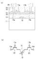
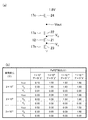
次に、図12(b)に示すように、酸素雰囲気中で加熱してエッチングダメージを回復した後、基板11上に、PLD法を用いて、基板温度を700℃にした状態で、厚さ450nmのPZT膜13を成長する。このときのターゲットに用いる焼結体の組成は、Pb:Zr:Ti=1:0.52:0.48である。この組成比で形成したPZT膜13と、STO基板11及びSRO膜12との格子ミスマッチは3%以内であり、上記の成長条件下でSRO膜12及びPZT膜13はエピタキシャル成長することができる。この方法で成膜したPZT膜13の表面を原子間力顕微鏡(AFM)で観察したところ、平均二乗粗さは3nm以下と極めて平滑であった。
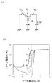
12 ゲート電極
13 強誘電体膜
14 半導体膜
15a〜15f ソース・ドレイン電極
16 常誘電体膜
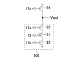
17a、17b、17c ゲート電極
18 層間絶縁膜
19 タングステンプラグ
20 アルミニウム配線
21 メモリ素子
22、23 選択スイッチング素子
24 負荷素子
30 第1のワード線
40 第2のワード線
50 第3のワード線
70 ソース線
80 ビット線
100 メモリセル
Claims (6)
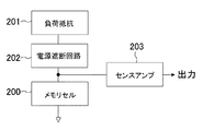
- 強誘電体膜からなるゲート絶縁膜と、半導体膜からなるチャネルとを有する第1の電界効果トランジスタで構成されたメモリセルと、
前記メモリセルに直列に接続された読み出し用の負荷素子と
を備えた半導体記憶装置であって、
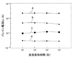
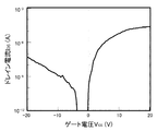
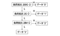
前記メモリセルは、前記強誘電体膜の分極状態に応じた、少なくとも3値以上のチャネル抵抗値を多値データとして記憶しており、
前記メモリセルに記憶された多値データは、前記メモリセルと前記負荷素子との間の中間電位を検出することによって読み出され、
前記読み出し動作は、前記メモリセルに記憶された多値データを、前記チャネル抵抗値の高い状態から順に判別することによって実行される、半導体記憶装置。 - 前記読み出し動作は、前記負荷素子の抵抗値を、前記チャネル抵抗値に応じて、該チャネル抵抗値の高い状態から順に変化させながら実行される、請求項1に記載の半導体記憶装置。
- 前記負荷素子は、第2の電界効果トランジスタで構成されており、
前記読み出し動作は、前記第2の電界効果トランジスタのゲート電極に印加する電圧を変化させることによって、前記負荷素子の抵抗値を変化させながら実行される、請求項2に記載の半導体記憶装置。 - 前記第2の電界効果トランジスタのチャネルは、前記第1の電界効果トランジスタのチャネルと共通の前記半導体膜からなる、請求項3に記載の半導体記憶装置。
- 前記メモリセルは、複数配列されており、
前記読み出し動作において、多値データが判別されたメモリセルは、該メモリセルの通電が遮断される、請求項1に記載の半導体記憶装置。 - 前記読み出し動作において、前記強誘電体膜に印加される電圧は、該強誘電体膜の分極状態を変化させない値に設定される、請求項1に記載の半導体記憶装置。
Priority Applications (2)
| Application Number | Priority Date | Filing Date | Title |
|---|---|---|---|
| JP2008150276A JP5081069B2 (ja) | 2008-06-09 | 2008-06-09 | 半導体記憶装置 |
| US12/405,799 US8004871B2 (en) | 2008-05-26 | 2009-03-17 | Semiconductor memory device including FET memory elements |
Applications Claiming Priority (1)
| Application Number | Priority Date | Filing Date | Title |
|---|---|---|---|
| JP2008150276A JP5081069B2 (ja) | 2008-06-09 | 2008-06-09 | 半導体記憶装置 |
Publications (2)
| Publication Number | Publication Date |
|---|---|
| JP2009295255A JP2009295255A (ja) | 2009-12-17 |
| JP5081069B2 true JP5081069B2 (ja) | 2012-11-21 |
Family
ID=41543291
Family Applications (1)
| Application Number | Title | Priority Date | Filing Date |
|---|---|---|---|
| JP2008150276A Expired - Fee Related JP5081069B2 (ja) | 2008-05-26 | 2008-06-09 | 半導体記憶装置 |
Country Status (1)
| Country | Link |
|---|---|
| JP (1) | JP5081069B2 (ja) |
Families Citing this family (7)
| Publication number | Priority date | Publication date | Assignee | Title |
|---|---|---|---|---|
| WO2012153448A1 (ja) * | 2011-05-09 | 2012-11-15 | パナソニック株式会社 | Rc発振回路 |
| JP5158294B2 (ja) * | 2011-06-06 | 2013-03-06 | パナソニック株式会社 | Rc発振回路 |
| US9337210B2 (en) * | 2013-08-12 | 2016-05-10 | Micron Technology, Inc. | Vertical ferroelectric field effect transistor constructions, constructions comprising a pair of vertical ferroelectric field effect transistors, vertical strings of ferroelectric field effect transistors, and vertical strings of laterally opposing pairs of vertical ferroelectric field effect transistors |
| US9472560B2 (en) | 2014-06-16 | 2016-10-18 | Micron Technology, Inc. | Memory cell and an array of memory cells |
| US9305929B1 (en) | 2015-02-17 | 2016-04-05 | Micron Technology, Inc. | Memory cells |
| US10134982B2 (en) | 2015-07-24 | 2018-11-20 | Micron Technology, Inc. | Array of cross point memory cells |
| JP2021057446A (ja) | 2019-09-30 | 2021-04-08 | ソニーセミコンダクタソリューションズ株式会社 | 半導体素子、不揮発性記憶装置、積和演算装置、及び半導体素子の製造方法 |
Family Cites Families (4)
| Publication number | Priority date | Publication date | Assignee | Title |
|---|---|---|---|---|
| JP2921812B2 (ja) * | 1992-12-24 | 1999-07-19 | シャープ株式会社 | 不揮発性半導体記憶装置 |
| JP2001102465A (ja) * | 1999-09-30 | 2001-04-13 | Rohm Co Ltd | 不揮発性メモリ |
| JP2002270789A (ja) * | 2001-03-14 | 2002-09-20 | Toshiba Corp | 強誘電体メモリ |
| JP4785180B2 (ja) * | 2004-09-10 | 2011-10-05 | 富士通セミコンダクター株式会社 | 強誘電体メモリ、多値データ記録方法、および多値データ読出し方法 |
-
2008
- 2008-06-09 JP JP2008150276A patent/JP5081069B2/ja not_active Expired - Fee Related
Also Published As
| Publication number | Publication date |
|---|---|
| JP2009295255A (ja) | 2009-12-17 |
Similar Documents
| Publication | Publication Date | Title |
|---|---|---|
| US8004871B2 (en) | Semiconductor memory device including FET memory elements | |
| JP5190275B2 (ja) | 半導体メモリセル及びそれを用いた半導体メモリアレイ | |
| US8385099B2 (en) | Semiconductor memory cell and manufacturing method thereof, and semiconductor memory devices | |
| US11101291B2 (en) | Memory cell arrangement and methods thereof | |
| US8023309B2 (en) | Semiconductor memory device, method for fabricating the same and semiconductor switching device | |
| US7772029B2 (en) | Memory element and memory device comprising memory layer positioned between first and second electrodes | |
| JP4894757B2 (ja) | 抵抗記憶素子及び不揮発性半導体記憶装置 | |
| US8023318B2 (en) | Resistance memory element, phase change memory element, resistance random access memory device, information reading method thereof, phase change random access memory device, and information reading method thereof | |
| JP5081069B2 (ja) | 半導体記憶装置 | |
| CN1790719B (zh) | 包括一电阻器和一晶体管的非易失存储器件 | |
| WO2019191393A1 (en) | Systems and methods for gated-insulator reconfigurable non-volatile memory devices | |
| JP2010267704A (ja) | 半導体メモリセルおよびその製造方法 | |
| JP2010267705A (ja) | 半導体メモリセルおよびその製造方法 | |
| TW202005001A (zh) | 半導體裝置以及其製作方法 | |
| US5977577A (en) | Ferroelectric based memory devices utilizing low curie point ferroelectrics and encapsulation | |
| JPWO2007046144A1 (ja) | 抵抗記憶素子及び不揮発性半導体記憶装置 | |
| US6194751B1 (en) | Ferroelectric based memory devices utilizing low Curie point ferroelectrics and encapsulation | |
| JP2008263019A (ja) | 半導体メモリセル及びその製造方法 | |
| CN103247627B (zh) | 半导体存储器件及其访问方法 | |
| JP2009283877A (ja) | 半導体記憶装置 | |
| RU2785593C1 (ru) | Элемент постоянной памяти на основе проводящего ферроэлектрика GeTe | |
| JP2008166486A (ja) | 半導体記憶素子 | |
| WO2024148515A1 (zh) | 多态单元及其制备方法、阵列和忆阻器 | |
| JPH05160410A (ja) | 電界効果トランジスタおよびその製造方法、ならびにそのトランジスタを用いた不揮発性記憶素子および不揮発性記憶装置 | |
| JP2001267518A (ja) | 強誘電体メモリ |
Legal Events
| Date | Code | Title | Description |
|---|---|---|---|
| A621 | Written request for application examination |
Free format text: JAPANESE INTERMEDIATE CODE: A621 Effective date: 20101116 |
|
| RD02 | Notification of acceptance of power of attorney |
Free format text: JAPANESE INTERMEDIATE CODE: A7422 Effective date: 20120201 |
|
| TRDD | Decision of grant or rejection written | ||
| A01 | Written decision to grant a patent or to grant a registration (utility model) |
Free format text: JAPANESE INTERMEDIATE CODE: A01 Effective date: 20120807 |
|
| A01 | Written decision to grant a patent or to grant a registration (utility model) |
Free format text: JAPANESE INTERMEDIATE CODE: A01 |
|
| A61 | First payment of annual fees (during grant procedure) |
Free format text: JAPANESE INTERMEDIATE CODE: A61 Effective date: 20120831 |
|
| FPAY | Renewal fee payment (event date is renewal date of database) |
Free format text: PAYMENT UNTIL: 20150907 Year of fee payment: 3 |
|
| R150 | Certificate of patent or registration of utility model |
Free format text: JAPANESE INTERMEDIATE CODE: R150 |
|
| LAPS | Cancellation because of no payment of annual fees |