WO2019013286A1 - 半導体装置 - Google Patents
半導体装置 Download PDFInfo
- Publication number
- WO2019013286A1 WO2019013286A1 PCT/JP2018/026339 JP2018026339W WO2019013286A1 WO 2019013286 A1 WO2019013286 A1 WO 2019013286A1 JP 2018026339 W JP2018026339 W JP 2018026339W WO 2019013286 A1 WO2019013286 A1 WO 2019013286A1
- Authority
- WO
- WIPO (PCT)
- Prior art keywords
- region
- surface side
- lifetime control
- control region
- semiconductor device
- Prior art date
- Legal status (The legal status is an assumption and is not a legal conclusion. Google has not performed a legal analysis and makes no representation as to the accuracy of the status listed.)
- Ceased
Links
Images












Classifications
-
- H—ELECTRICITY
- H10—SEMICONDUCTOR DEVICES; ELECTRIC SOLID-STATE DEVICES NOT OTHERWISE PROVIDED FOR
- H10P—GENERIC PROCESSES OR APPARATUS FOR THE MANUFACTURE OR TREATMENT OF DEVICES COVERED BY CLASS H10
- H10P32/00—Diffusion of dopants within, into or out of wafers, substrates or parts of devices
- H10P32/10—Diffusion of dopants within, into or out of semiconductor bodies or layers
- H10P32/18—Diffusion lifetime killers
-
- H—ELECTRICITY
- H10—SEMICONDUCTOR DEVICES; ELECTRIC SOLID-STATE DEVICES NOT OTHERWISE PROVIDED FOR
- H10D—INORGANIC ELECTRIC SEMICONDUCTOR DEVICES
- H10D12/00—Bipolar devices controlled by the field effect, e.g. insulated-gate bipolar transistors [IGBT]
- H10D12/01—Manufacture or treatment
- H10D12/031—Manufacture or treatment of IGBTs
- H10D12/032—Manufacture or treatment of IGBTs of vertical IGBTs
- H10D12/038—Manufacture or treatment of IGBTs of vertical IGBTs having a recessed gate, e.g. trench-gate IGBTs
-
- H—ELECTRICITY
- H10—SEMICONDUCTOR DEVICES; ELECTRIC SOLID-STATE DEVICES NOT OTHERWISE PROVIDED FOR
- H10D—INORGANIC ELECTRIC SEMICONDUCTOR DEVICES
- H10D12/00—Bipolar devices controlled by the field effect, e.g. insulated-gate bipolar transistors [IGBT]
- H10D12/411—Insulated-gate bipolar transistors [IGBT]
- H10D12/441—Vertical IGBTs
- H10D12/461—Vertical IGBTs having non-planar surfaces, e.g. having trenches, recesses or pillars in the surfaces of the emitter, base or collector regions
- H10D12/481—Vertical IGBTs having non-planar surfaces, e.g. having trenches, recesses or pillars in the surfaces of the emitter, base or collector regions having gate structures on slanted surfaces, on vertical surfaces, or in grooves, e.g. trench gate IGBTs
-
- H—ELECTRICITY
- H10—SEMICONDUCTOR DEVICES; ELECTRIC SOLID-STATE DEVICES NOT OTHERWISE PROVIDED FOR
- H10D—INORGANIC ELECTRIC SEMICONDUCTOR DEVICES
- H10D30/00—Field-effect transistors [FET]
- H10D30/60—Insulated-gate field-effect transistors [IGFET]
-
- H—ELECTRICITY
- H10—SEMICONDUCTOR DEVICES; ELECTRIC SOLID-STATE DEVICES NOT OTHERWISE PROVIDED FOR
- H10D—INORGANIC ELECTRIC SEMICONDUCTOR DEVICES
- H10D62/00—Semiconductor bodies, or regions thereof, of devices having potential barriers
- H10D62/10—Shapes, relative sizes or dispositions of the regions of the semiconductor bodies; Shapes of the semiconductor bodies
-
- H—ELECTRICITY
- H10—SEMICONDUCTOR DEVICES; ELECTRIC SOLID-STATE DEVICES NOT OTHERWISE PROVIDED FOR
- H10D—INORGANIC ELECTRIC SEMICONDUCTOR DEVICES
- H10D62/00—Semiconductor bodies, or regions thereof, of devices having potential barriers
- H10D62/10—Shapes, relative sizes or dispositions of the regions of the semiconductor bodies; Shapes of the semiconductor bodies
- H10D62/102—Constructional design considerations for preventing surface leakage or controlling electric field concentration
- H10D62/112—Constructional design considerations for preventing surface leakage or controlling electric field concentration for preventing surface leakage due to surface inversion layers, e.g. by using channel stoppers
-
- H—ELECTRICITY
- H10—SEMICONDUCTOR DEVICES; ELECTRIC SOLID-STATE DEVICES NOT OTHERWISE PROVIDED FOR
- H10D—INORGANIC ELECTRIC SEMICONDUCTOR DEVICES
- H10D62/00—Semiconductor bodies, or regions thereof, of devices having potential barriers
- H10D62/10—Shapes, relative sizes or dispositions of the regions of the semiconductor bodies; Shapes of the semiconductor bodies
- H10D62/124—Shapes, relative sizes or dispositions of the regions of semiconductor bodies or of junctions between the regions
- H10D62/126—Top-view geometrical layouts of the regions or the junctions
- H10D62/127—Top-view geometrical layouts of the regions or the junctions of cellular field-effect devices, e.g. multicellular DMOS transistors or IGBTs
-
- H—ELECTRICITY
- H10—SEMICONDUCTOR DEVICES; ELECTRIC SOLID-STATE DEVICES NOT OTHERWISE PROVIDED FOR
- H10D—INORGANIC ELECTRIC SEMICONDUCTOR DEVICES
- H10D62/00—Semiconductor bodies, or regions thereof, of devices having potential barriers
- H10D62/10—Shapes, relative sizes or dispositions of the regions of the semiconductor bodies; Shapes of the semiconductor bodies
- H10D62/129—Cathode regions of diodes
-
- H—ELECTRICITY
- H10—SEMICONDUCTOR DEVICES; ELECTRIC SOLID-STATE DEVICES NOT OTHERWISE PROVIDED FOR
- H10D—INORGANIC ELECTRIC SEMICONDUCTOR DEVICES
- H10D62/00—Semiconductor bodies, or regions thereof, of devices having potential barriers
- H10D62/10—Shapes, relative sizes or dispositions of the regions of the semiconductor bodies; Shapes of the semiconductor bodies
- H10D62/13—Semiconductor regions connected to electrodes carrying current to be rectified, amplified or switched, e.g. source or drain regions
- H10D62/141—Anode or cathode regions of thyristors; Collector or emitter regions of gated bipolar-mode devices, e.g. of IGBTs
-
- H—ELECTRICITY
- H10—SEMICONDUCTOR DEVICES; ELECTRIC SOLID-STATE DEVICES NOT OTHERWISE PROVIDED FOR
- H10D—INORGANIC ELECTRIC SEMICONDUCTOR DEVICES
- H10D62/00—Semiconductor bodies, or regions thereof, of devices having potential barriers
- H10D62/10—Shapes, relative sizes or dispositions of the regions of the semiconductor bodies; Shapes of the semiconductor bodies
- H10D62/13—Semiconductor regions connected to electrodes carrying current to be rectified, amplified or switched, e.g. source or drain regions
- H10D62/141—Anode or cathode regions of thyristors; Collector or emitter regions of gated bipolar-mode devices, e.g. of IGBTs
- H10D62/142—Anode regions of thyristors or collector regions of gated bipolar-mode devices
-
- H—ELECTRICITY
- H10—SEMICONDUCTOR DEVICES; ELECTRIC SOLID-STATE DEVICES NOT OTHERWISE PROVIDED FOR
- H10D—INORGANIC ELECTRIC SEMICONDUCTOR DEVICES
- H10D62/00—Semiconductor bodies, or regions thereof, of devices having potential barriers
- H10D62/10—Shapes, relative sizes or dispositions of the regions of the semiconductor bodies; Shapes of the semiconductor bodies
- H10D62/17—Semiconductor regions connected to electrodes not carrying current to be rectified, amplified or switched, e.g. channel regions
- H10D62/393—Body regions of DMOS transistors or IGBTs
-
- H—ELECTRICITY
- H10—SEMICONDUCTOR DEVICES; ELECTRIC SOLID-STATE DEVICES NOT OTHERWISE PROVIDED FOR
- H10D—INORGANIC ELECTRIC SEMICONDUCTOR DEVICES
- H10D62/00—Semiconductor bodies, or regions thereof, of devices having potential barriers
- H10D62/50—Physical imperfections
- H10D62/53—Physical imperfections the imperfections being within the semiconductor body
-
- H—ELECTRICITY
- H10—SEMICONDUCTOR DEVICES; ELECTRIC SOLID-STATE DEVICES NOT OTHERWISE PROVIDED FOR
- H10D—INORGANIC ELECTRIC SEMICONDUCTOR DEVICES
- H10D62/00—Semiconductor bodies, or regions thereof, of devices having potential barriers
- H10D62/60—Impurity distributions or concentrations
-
- H—ELECTRICITY
- H10—SEMICONDUCTOR DEVICES; ELECTRIC SOLID-STATE DEVICES NOT OTHERWISE PROVIDED FOR
- H10D—INORGANIC ELECTRIC SEMICONDUCTOR DEVICES
- H10D64/00—Electrodes of devices having potential barriers
- H10D64/111—Field plates
-
- H—ELECTRICITY
- H10—SEMICONDUCTOR DEVICES; ELECTRIC SOLID-STATE DEVICES NOT OTHERWISE PROVIDED FOR
- H10D—INORGANIC ELECTRIC SEMICONDUCTOR DEVICES
- H10D8/00—Diodes
- H10D8/422—PN diodes having the PN junctions in mesas
-
- H—ELECTRICITY
- H10—SEMICONDUCTOR DEVICES; ELECTRIC SOLID-STATE DEVICES NOT OTHERWISE PROVIDED FOR
- H10D—INORGANIC ELECTRIC SEMICONDUCTOR DEVICES
- H10D84/00—Integrated devices formed in or on semiconductor substrates that comprise only semiconducting layers, e.g. on Si wafers or on GaAs-on-Si wafers
- H10D84/60—Integrated devices formed in or on semiconductor substrates that comprise only semiconducting layers, e.g. on Si wafers or on GaAs-on-Si wafers characterised by the integration of at least one component covered by groups H10D10/00 or H10D18/00, e.g. integration of BJTs
- H10D84/611—Combinations of BJTs and one or more of diodes, resistors or capacitors
- H10D84/613—Combinations of vertical BJTs and one or more of diodes, resistors or capacitors
- H10D84/617—Combinations of vertical BJTs and only diodes
-
- H—ELECTRICITY
- H10—SEMICONDUCTOR DEVICES; ELECTRIC SOLID-STATE DEVICES NOT OTHERWISE PROVIDED FOR
- H10D—INORGANIC ELECTRIC SEMICONDUCTOR DEVICES
- H10D84/00—Integrated devices formed in or on semiconductor substrates that comprise only semiconducting layers, e.g. on Si wafers or on GaAs-on-Si wafers
- H10D84/80—Integrated devices formed in or on semiconductor substrates that comprise only semiconducting layers, e.g. on Si wafers or on GaAs-on-Si wafers characterised by the integration of at least one component covered by groups H10D12/00 or H10D30/00, e.g. integration of IGFETs
- H10D84/811—Combinations of field-effect devices and one or more diodes, capacitors or resistors
-
- H—ELECTRICITY
- H10—SEMICONDUCTOR DEVICES; ELECTRIC SOLID-STATE DEVICES NOT OTHERWISE PROVIDED FOR
- H10P—GENERIC PROCESSES OR APPARATUS FOR THE MANUFACTURE OR TREATMENT OF DEVICES COVERED BY CLASS H10
- H10P32/00—Diffusion of dopants within, into or out of wafers, substrates or parts of devices
- H10P32/10—Diffusion of dopants within, into or out of semiconductor bodies or layers
- H10P32/17—Diffusion of dopants within, into or out of semiconductor bodies or layers characterised by the semiconductor material
- H10P32/171—Diffusion of dopants within, into or out of semiconductor bodies or layers characterised by the semiconductor material being group IV material
-
- H—ELECTRICITY
- H10—SEMICONDUCTOR DEVICES; ELECTRIC SOLID-STATE DEVICES NOT OTHERWISE PROVIDED FOR
- H10D—INORGANIC ELECTRIC SEMICONDUCTOR DEVICES
- H10D64/00—Electrodes of devices having potential barriers
- H10D64/111—Field plates
- H10D64/117—Recessed field plates, e.g. trench field plates or buried field plates
-
- H—ELECTRICITY
- H10—SEMICONDUCTOR DEVICES; ELECTRIC SOLID-STATE DEVICES NOT OTHERWISE PROVIDED FOR
- H10P—GENERIC PROCESSES OR APPARATUS FOR THE MANUFACTURE OR TREATMENT OF DEVICES COVERED BY CLASS H10
- H10P30/00—Ion implantation into wafers, substrates or parts of devices
- H10P30/20—Ion implantation into wafers, substrates or parts of devices into semiconductor materials, e.g. for doping
- H10P30/202—Ion implantation into wafers, substrates or parts of devices into semiconductor materials, e.g. for doping characterised by the semiconductor materials
- H10P30/204—Ion implantation into wafers, substrates or parts of devices into semiconductor materials, e.g. for doping characterised by the semiconductor materials into Group IV semiconductors
-
- H—ELECTRICITY
- H10—SEMICONDUCTOR DEVICES; ELECTRIC SOLID-STATE DEVICES NOT OTHERWISE PROVIDED FOR
- H10P—GENERIC PROCESSES OR APPARATUS FOR THE MANUFACTURE OR TREATMENT OF DEVICES COVERED BY CLASS H10
- H10P30/00—Ion implantation into wafers, substrates or parts of devices
- H10P30/20—Ion implantation into wafers, substrates or parts of devices into semiconductor materials, e.g. for doping
- H10P30/208—Ion implantation into wafers, substrates or parts of devices into semiconductor materials, e.g. for doping of electrically inactive species
Definitions
- the present invention relates to a semiconductor device.
- Patent Document 1 JP-A-2017-41601
- Patent Document 2 JP-A-2012-43891
- a semiconductor substrate having a drift region of a first conductivity type, a transistor part provided on the semiconductor substrate, and the semiconductor part provided on the semiconductor substrate and arranged along a predetermined arrangement direction And a diode unit arranged in the semiconductor device.
- Both the transistor part and the diode part may have a base region of the second conductivity type provided above the drift region inside the semiconductor substrate.
- Both the transistor portion and the diode portion penetrate the base region from the upper surface of the semiconductor substrate, extend in the extending direction perpendicular to the arrangement direction on the upper surface of the semiconductor substrate, and have a plurality of trench portions provided with the conductive portions therein.
- Both the transistor part and the diode part may be provided on the lower surface side of the semiconductor substrate from the transistor part to the diode part, and may have a lower surface side lifetime control region including a lifetime killer.
- the lower surface side lifetime control region may be provided in a part of the transistor portion in the arrangement direction and may not be provided in the other part.
- the lower surface side lifetime control region may be provided in a part of the diode section in the arrangement direction and not in another part.
- the diode portion is a cathode region of the first conductivity type exposed on the lower surface of the semiconductor substrate, and a floating region of the second conductivity type electrically floating provided on the lower surface side of the semiconductor substrate And may be included.
- the floating region may cover a portion of the cathode region above the cathode region.
- the floating region may be provided on the lower surface side of the semiconductor substrate than the lower surface side lifetime control region. In a top view of the semiconductor substrate, at least a part of the floating region may overlap the lower surface side lifetime control region.
- a plurality of floating regions may be provided in the arrangement direction. In the top view of the semiconductor substrate, at least one floating region of the plurality of floating regions may not overlap the lower surface side lifetime control region in the arrangement direction.
- the lower surface side lifetime control region may be provided in the entire diode section in the arrangement direction. In the arrangement direction, the length of the lower surface side lifetime control region in the transistor portion may be longer than the length of the lower surface side lifetime control region in the diode portion.
- the semiconductor device may further include an upper surface side lifetime control region provided on the upper surface side of the semiconductor substrate from the transistor portion to the diode portion and including a lifetime killer.
- the lower surface side lifetime control region may be provided closer to the diode portion in the arrangement direction than the upper surface side lifetime control region.
- the semiconductor device may further include a collector region provided on the lower surface of the semiconductor substrate.
- a collector region may be provided on the extension of the path from the end of the upper surface side lifetime control region in the transistor portion to the end of the lower surface side lifetime control region in the transistor portion in the arrangement direction.
- the lower surface side lifetime control region may be provided closer to the transistor portion in the arrangement direction than the upper surface side lifetime control region.
- the lifetime killer concentration of the lower surface side lifetime control region may be higher than the lifetime killer concentration of the upper surface side lifetime control region.
- the length of the upper surface side lifetime control region in the transistor portion may be not less than 0.01 times and not more than 0.15 times the length of the transistor portion.
- the distance in the direction parallel to the lower surface of the semiconductor substrate between the end of the upper surface side lifetime control region of the transistor portion and the end of the lower surface side lifetime control region of the transistor portion is the upper surface side of the transistor portion
- the length may be 0.25 times or more and 0.5 times or less the length of the lifetime control region.
- the lower surface side lifetime control region may be provided to the outside of the upper surface side lifetime control region in the stretching direction.
- the length of the upper surface side lifetime control region may be larger than the thickness of the semiconductor substrate.
- a plurality of lower surface side lifetime control regions may be provided in the depth direction of the semiconductor substrate.
- the lower surface side lifetime control region provided on the lower surface side of the semiconductor substrate is provided closer to the diode portion in the arrangement direction than the lower surface lifetime control region provided on the upper surface side of the semiconductor substrate. It may be done.
- a portion from the end of the lower surface side lifetime control region provided on the upper surface side of the semiconductor substrate to the end portion of the lower surface side lifetime control region provided on the lower surface side of the semiconductor substrate has a convex shape It may be located at
- the lower surface side lifetime control region provided on the lower surface side of the semiconductor substrate is provided closer to the diode portion in the arrangement direction than the lower surface lifetime control region provided on the upper surface side of the semiconductor substrate. It may be done.
- the lifetime killer concentration of the lower surface side lifetime control region provided on the lower surface side of the semiconductor substrate may be higher than the lifetime killer concentration of the lower surface side lifetime control region provided on the upper surface side of the semiconductor substrate.
- the length of the lower surface side lifetime control region in the diode portion may be not less than 0.015 times and not more than 0.03 times the length of the diode portion.
- the semiconductor device may further include a buffer region of the first conductivity type provided below the drift region, from the transistor portion to the diode portion.
- the lower surface side lifetime control area may be provided in the buffer area.
- the semiconductor device may further include a buffer region of the first conductivity type provided below the drift region, from the transistor portion to the diode portion.
- the thickness of the buffer area provided below the lower surface side lifetime control area may be larger than the thickness of the buffer area not provided below the lower surface side lifetime control area.
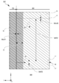
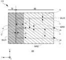
- FIG. 1 It is a figure which shows partially the upper surface of the semiconductor device 100 which concerns on embodiment of this invention. It is a figure which shows an example of the aa 'cross section in FIG. It is a figure which shows another example of the aa 'cross section in FIG. It is a figure which shows another example of the aa 'cross section in FIG. It is a figure which shows another example of the aa 'cross section in FIG. It is a figure which shows partially the upper surface of the semiconductor device 150 of a comparative example. It is a figure which shows an example of the aa-aa 'cross section in FIG. FIG.
- FIG. 7 is a view showing an example of lifetime killer concentration distributions of the upper surface side lifetime control region 72 and the lower surface side lifetime control region 74 in the bb ′ cross section of FIG. 2; It is a figure which shows another example of the aa 'cross section in FIG. It is a figure which shows another example of the aa 'cross section in FIG.
- FIG. 10 is a view showing an example of lifetime killer concentration distributions of the upper surface side lifetime control region 72 and the lower surface side lifetime control region 74-1 to the lower surface side lifetime control region 74-4 in the ff 'cross section of FIG. 9; It is a figure which shows an example of the semiconductor chip 98 which concerns on embodiment of this invention. It is an enlarged view of the area
- FIG. 13 is a view showing another example of the gg ′ cross section in FIG. 12;
- FIG. 13 is a view showing another example of the gg ′ cross section in FIG. 12;
- 17 is a view showing an example of lifetime killer concentration distribution in the Y-axis direction of the lower surface side lifetime control region 74-4 in the hh 'cross section of FIG. 15 and the jj' cross section of FIG. 16;
- It is a figure which shows partially the upper surface of the other semiconductor device 200 which concerns on this embodiment. It is an enlarged view of the area
- FIG. 19 is a view showing an example of a qq 'cross section in FIG. 18;
- FIG. 19 is a view showing an example of a qq 'cross section in FIG. 18;
- FIG. 19 is a view showing an example of a qq 'cross section in FIG. 18;
- FIG. 19 is a view showing an example of a qq 'cross section in FIG.
- FIG. 21 is a cross-sectional view taken along the line kk ′ in FIG. 20, including the transistor section 70 adjacent to the Y axis negative side of the diode section 80. It is a figure showing an example of the upper surface of semiconductor chip 120 concerning this embodiment. It is an enlarged view of area
- FIG. 24 is a view showing an example of a hh ′ cross section in FIG. 23; FIG. 24 is a view showing an example of a jj ′ cross section in FIG. 23; FIG. 23 is another enlarged view of a region A1 in FIG. 22.
- FIG. 29 is an enlarged view of a region C1 in FIG. 28.
- FIG. 30 is an enlarged view of a region C2 in FIG. 29. It is a figure which shows an example of the kk 'cross section in FIG.
- FIG. 29 is a view showing an example of the m-m 'cross section in FIG. 28.
- one side in a direction parallel to the depth direction of the semiconductor substrate is referred to as “upper”, and the other side is referred to as “lower”.
- the upper surface is referred to as the upper surface
- the other surface is referred to as the lower surface.
- the directions of “upper” and “lower” are not limited to the direction of gravity or the mounting direction to a substrate or the like at the time of mounting of the semiconductor device.
- the first conductivity type is N-type and the second conductivity type is P-type is shown, but the first conductivity type may be P-type and the second conductivity type may be N-type.
- the conductivity types of the substrate, layer, region and the like in the respective embodiments have opposite polarities.
- doping concentration refers to the concentration of donor or acceptor turned impurities.
- concentration difference between the donor and the acceptor may be referred to as the doping concentration.
- the peak value may be used as the doping concentration in the doping region.
- the average value of the doping concentrations in the doping region may be used as the doping concentration.
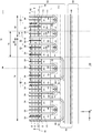
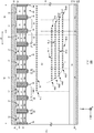
- FIG. 1 is a view partially showing an example of an upper surface of a semiconductor device 100 according to an embodiment of the present invention.
- the semiconductor device 100 of this example is a semiconductor chip provided with a transistor unit 70 and a diode unit 80.
- the transistor unit 70 includes a transistor such as an IGBT.
- the diode unit 80 includes a diode such as a free wheel diode (FWD) provided parallel to the transistor unit 70 on the upper surface of the semiconductor substrate.
- FWD free wheel diode
- a region located at the boundary between the transistor unit 70 and the diode unit 80 is a boundary unit 90.
- FIG. 1 the chip top surface around the chip end is shown, and other regions are omitted.
- FIG. 1 shows the active region of the semiconductor substrate in the semiconductor device 100
- the semiconductor device 100 may have an edge termination structure portion surrounding the active region.
- the active region indicates a region through which current flows when the semiconductor device 100 is controlled to be in an on state.
- the edge termination structure mitigates the concentration of the electric field on the upper surface side of the semiconductor substrate.
- the edge termination structure has, for example, a guard ring, a field plate, a resurf and a combination thereof.
- the semiconductor device 100 of this example is provided inside the semiconductor substrate, and the gate trench portion 40, the dummy trench portion 30, the well region 11, the emitter region 12, the base region 14 and the contact region 15 exposed on the upper surface of the semiconductor substrate. Equipped with, the semiconductor device 100 of this example includes the emitter electrode 52 and the gate metal layer 50 provided above the upper surface of the semiconductor substrate. Emitter electrode 52 and gate metal layer 50 are provided separately from each other.
- An interlayer insulating film is provided between the emitter electrode 52 and the gate metal layer 50 and the upper surface of the semiconductor substrate, but is omitted in FIG.
- the contact hole 56, the contact hole 49 and the contact hole 54 are provided to penetrate the interlayer insulating film.
- emitter electrode 52 is connected to the dummy conductive portion in dummy trench portion 30 through contact hole 56. Between the emitter electrode 52 and the dummy conductive portion, a connection portion 25 formed of a conductive material such as polysilicon doped with an impurity may be provided. An insulating film such as an oxide film is provided between the connection portion 25 and the upper surface of the semiconductor substrate.
- the gate metal layer 50 contacts the gate runner 48 through the contact hole 49.
- the gate runner 48 is formed of polysilicon doped with an impurity. Gate runner 48 is connected to the gate conductive portion in gate trench portion 40 on the upper surface of the semiconductor substrate. Gate runner 48 is not connected to the dummy conductive portion in dummy trench portion 30.
- the gate runner 48 in this example is provided from the lower side of the contact hole 49 to the tip of the gate trench portion 40.
- An insulating film such as an oxide film is provided between the gate runner 48 and the upper surface of the semiconductor substrate.
- the gate conductive portion is exposed on the upper surface of the semiconductor substrate.
- the gate trench portion 40 contacts the gate runner 48 at the exposed portion of the gate conductive portion.
- Emitter electrode 52 and gate metal layer 50 are formed of a material containing a metal.
- each electrode is formed of aluminum or aluminum-silicon alloy.
- Each electrode may have a barrier metal formed of titanium, a titanium compound, or the like below the region formed of aluminum or the like.
- Each electrode may have a plug formed of tungsten or the like in the contact hole.
- the one or more gate trench portions 40 and the one or more dummy trench portions 30 are arranged at predetermined intervals along a predetermined arrangement direction (in this example, the Y-axis direction).
- the gate trench portion 40 in this example is formed by two extending portions 39 extending in parallel with the upper surface of the semiconductor substrate and extending in the extending direction (in this example, the X-axis direction) perpendicular to the arrangement direction; May have a connecting portion 41 connecting the two.
- at least a portion of the connection portion 41 is provided in a curved shape.
- the dummy trench portion 30 in the present example may have a U-shape on the upper surface of the semiconductor substrate, similarly to the gate trench portion 40. That is, the dummy trench portion 30 in this example may have two extension portions 29 extending in the extension direction and a connection portion 31 connecting the two extension portions 29.
- Emitter electrode 52 is provided above gate trench portion 40, dummy trench portion 30, well region 11, emitter region 12, base region 14 and contact region 15.
- Well region 11 is of the second conductivity type.
- Well region 11 is provided in a predetermined range from the end of the active region on the side where gate metal layer 50 is provided.
- the diffusion depth of the well region 11 may be deeper than the depths of the gate trench portion 40 and the dummy trench portion 30.
- a partial region on the gate metal layer 50 side of the gate trench portion 40 and the dummy trench portion 30 is provided in the well region 11.
- the bottoms of the ends in the extending direction of the gate trench portion 40 and the dummy trench portion 30 may be covered with the well region 11.
- the contact holes 54 are provided above the contact region 15 and the emitter region 12, respectively.
- the contact hole 54 is provided above the base region 14. Neither contact hole 54 is disposed above the base region 14 and the well region 11 disposed at both ends in the X-axis direction.
- a mesa portion is provided in contact with each trench portion in the Y-axis direction in a direction parallel to the upper surface of the semiconductor substrate.
- the mesa portion may be a portion of the semiconductor substrate sandwiched between two adjacent trench portions, and may be a portion from the upper surface of the semiconductor substrate to the deepest bottom of each trench portion.
- the extension portion of each trench portion may be one trench portion. That is, the region between the two extending portions may be a mesa portion.
- a transistor mesa portion 60 is provided in contact with each trench portion.
- a boundary mesa portion 62 is provided in the boundary portion 90 in contact with each trench portion.
- the diode mesa portion 64 is provided in a region sandwiched by the adjacent dummy trench portions 30.
- Base regions 14 are provided, as an example, at both ends of the transistor mesa 60, the boundary mesa 62, and the diode mesa 64 in the X-axis direction. In FIG. 1, only the base region 14 provided at one end in the X-axis direction is shown.
- Emitter region 12 is provided on the upper surface of transistor mesa 60 in contact with gate trench portion 40.
- the emitter region 12 of this example is of the first conductivity type.
- a contact region 15 of the second conductivity type which has a doping concentration higher than that of the base region 14, is provided.
- the emitter regions 12 and the contact regions 15 may be alternately provided in the extending direction of the gate trench portion 40.
- the emitter region 12 and the contact region 15 are provided also below the contact hole 54.
- Emitter region 12 may be provided in contact with dummy trench portion 30 on the upper surface of transistor mesa portion 60 or may be provided separately. Emitter region 12 in the example of FIG. 1 is provided in contact with dummy trench portion 30.
- a contact region 15 of the second conductivity type having a doping concentration higher than that of the base region 14 is provided on the top surface of the boundary mesa portion 62.
- the contact regions 15 may be provided in the entire region sandwiched by the base regions 14 provided at both ends of the boundary mesa portion 62 in the X-axis direction. In the boundary mesa portion 62, the contact region 15 is also provided below the contact hole 54.
- Contact regions 15 are provided on the top surface of the diode mesa 64 at both ends in the X-axis direction.
- a base region 14 is provided in a region sandwiched by the contact regions 15.
- the base region 14 may be provided in the entire region sandwiched by the contact regions 15.
- the base region 14 and the contact region 15 are also provided below the contact hole 54.
- the dummy trench portion 30 is provided in the diode portion 80.
- the linear extension portions 29 of the respective dummy trench portions 30 are connected by the connection portion 31.
- a diode mesa portion 64 is provided in a region sandwiched by the respective dummy trench portions 30.
- the emitter region 12 may not be provided in the diode mesa portion 64, and may be provided. In this example, the emitter region 12 is not provided.
- the contact region 15 or the base region 14 is provided from one dummy trench portion 30 sandwiching the diode mesa portion 64 to the other dummy trench portion 30. That is, on the upper surface of the semiconductor substrate, the width of the diode mesa 64 in the Y-axis direction is equal to the width of the contact region 15 or the base region 14 provided in the diode mesa 64 in the Y-axis direction.
- the diode section 80 has a cathode region 82 of the first conductivity type on the lower surface side of the semiconductor substrate.
- a region where the cathode region 82 is provided in a top view of the semiconductor substrate is indicated by a dashed-dotted line portion.
- the diode section 80 may be an area where the cathode area 82 is projected on the upper surface of the semiconductor substrate.
- the region where the cathode region 82 is projected on the upper surface of the semiconductor substrate may be separated from the contact region 15 in the + X axis direction.
- a collector region of the second conductivity type may be provided in a region exposed to the lower surface of the semiconductor substrate and not provided with the cathode region 82.
- the transistor portion 70 may be a region in which a trench portion or a mesa portion is provided in a region obtained by projecting the collector region on the upper surface of the semiconductor substrate.
- the upper surface side lifetime control region 72 including the lifetime killer is provided locally in the depth direction of the semiconductor substrate.
- a region where the upper surface side lifetime control region 72 is provided in a top view of the semiconductor substrate is indicated by a broken line portion.
- the upper surface side lifetime control area 72 is provided up to the area not shown in FIG. 1 of the area on the Y axis negative side and the areas on the X axis positive side and the negative side in FIG.
- a direction perpendicular to the semiconductor substrate in a top view of the semiconductor substrate is referred to as a depth direction (Z-axis direction).
- the lower surface side lifetime control region 74 including the lifetime killer is locally provided below the upper surface side lifetime control region 72 in the depth direction of the semiconductor substrate.
- a region where the lower surface side lifetime control region 74 is provided in a top view of the semiconductor substrate is indicated by a broken line portion.
- the lower surface side lifetime control area 74 is provided up to the area not shown in FIG. 1 of the areas on the X axis positive side and the negative side in FIG. 1.
- the range in which the upper surface side lifetime control area 72 is provided in the Y-axis direction may be wider than the area in which the lower surface side lifetime control area 74 is provided.
- the entire trench portion in the region where the upper surface side lifetime control region 72 is provided may be the dummy trench portion 30 in top view.
- the particle beam may be irradiated from the upper surface side to form the upper surface side lifetime control area 72.
- the gate insulating film may be damaged.
- the trench portion in the upper surface side lifetime control region 72 as the dummy trench portion 30, the occurrence of damage to the gate insulating film can be suppressed. Therefore, gate threshold fluctuation of the transistor and gate insulating film breakdown can be prevented.
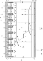
- FIG. 2 is a view showing an example of an aa ′ cross section in FIG.
- the aa ′ cross section is a YZ plane passing through the emitter region 12, the contact region 15 and the base region 14 in the transistor portion 70 and the diode portion 80.
- the semiconductor device 100 of this example has the semiconductor substrate 10, the interlayer insulating film 38, the emitter electrode 52, and the collector electrode 24 in the cross section aa '.
- Emitter electrode 52 is provided on upper surface 21 of semiconductor substrate 10 and the upper surface of interlayer insulating film 38.
- the collector electrode 24 is provided on the lower surface 23 of the semiconductor substrate 10. Emitter electrode 52 and collector electrode 24 are formed of a conductive material such as metal.
- the semiconductor substrate 10 may be a silicon substrate, a silicon carbide substrate, or a nitride semiconductor substrate such as gallium nitride.
- the semiconductor substrate 10 of this example is a silicon substrate.
- the semiconductor substrate 10 of this example includes the drift region 18 of the first conductivity type.
- the drift region 18 in this example is N + type.
- Drift region 18 may be a region remaining in semiconductor substrate 10 without forming another doping region. That is, the doping concentration of the drift region 18 may be the doping concentration of the semiconductor substrate 10.
- a buffer region 20 of the first conductivity type may be provided below the drift region 18.
- the doping concentration of buffer region 20 is higher than the doping concentration of drift region 18.
- Buffer region 20 may function as a field stop layer that prevents a depletion layer extending from the lower surface side of base region 14 from reaching collector region 22 and cathode region 82 of the second conductivity type.
- the diode portion 80 has a cathode region 82 below the buffer region 20.
- the cathode region 82 may be provided at the same depth as the collector region 22 of the transistor unit 70.
- the diode unit 80 may function as a free wheeling diode (FWD) that allows a return current to flow in the reverse direction when the transistor unit 70 of another semiconductor device 100 is turned off in a power conversion circuit such as an inverter.
- FWD free wheeling diode
- a collector region 22 of the second conductivity type is provided below the buffer region 20.
- the collector region 22 may extend to a region on the lower surface 23 side of the boundary mesa portion 62.
- the semiconductor device 100 of this example since the collector region 22 extends to the lower surface 23 of the boundary mesa portion 62, the distance between the emitter region 12 of the transistor portion 70 and the cathode region 82 of the diode portion 80 can be secured. Therefore, the semiconductor device 100 of this example can prevent the electrons injected from the gate structure including the emitter region 12 of the transistor unit 70 into the drift region 18 from flowing out into the cathode region 82 of the diode unit 80. .
- the distance between the contact region 15 of the boundary mesa portion 62 and the cathode region 82 of the diode portion 80 can also be longer than in the case where the cathode region 82 is provided immediately below the boundary mesa portion 62. Therefore, the semiconductor device 100 of this example can suppress the injection of holes from the contact region 15 having a doping concentration higher than that of the base region 14 to the cathode region 82 when the diode unit 80 conducts.
- the storage region 16 of the first conductivity type may be provided above the drift region 18.
- the accumulation region 16 is a region where the same dopant as the drift region 18 is accumulated at a higher concentration than the drift region 18.
- the doping concentration of storage region 16 is higher than the doping concentration of drift region 18.
- Storage region 16 is provided in contact with gate trench portion 40.
- a base region 14 of the second conductivity type is provided above the storage region 16 in the transistor mesa 60 and the boundary mesa 62.
- Base region 14 is provided in contact with gate trench portion 40.
- the emitter region 12 is provided between the base region 14 and the top surface 21 in the transistor mesa 60.
- Emitter region 12 is provided in contact with gate trench portion 40.
- the doping concentration of the emitter region 12 is higher than the doping concentration of the drift region 18.
- An example of the dopant of the emitter region 12 is arsenic (As).
- the contact region 15 of the second conductivity type is provided above the storage region 16 in the boundary mesa 62.
- Contact region 15 is provided in contact with gate trench portion 40.
- the emitter region 12 may not be provided.
- a storage region 16 is provided above the drift region 18 in the diode mesa 64. Further, in the present example, a base region 14 is provided above the storage region 16 in the diode mesa 64. Emitter region 12 may not be provided in diode mesa portion 64.
- the upper surface 21 is provided with one or more gate trench portions 40 and one or more dummy trench portions 30.
- Each trench portion is provided from the upper surface 21 to the drift region 18. In a region where at least one of emitter region 12, contact region 15 and storage region 16 is provided, each trench portion is also provided to penetrate drift region 18 to reach drift region 18.
- the fact that the trench portion penetrates the doping region is not limited to the one manufactured in the order of forming the doping region and then forming the trench portion. After forming the trench portion, those in which the doping region is formed between the trench portions are also included in those in which the trench portion penetrates the doping region.
- the gate trench portion 40 has a gate trench provided on the upper surface 21, a gate insulating film 42, and a gate conductive portion 44.
- the gate insulating film 42 is provided to cover the inner wall of the gate trench.
- the gate insulating film 42 may be formed by oxidizing or nitriding the semiconductor on the inner wall of the gate trench.
- the gate conductive portion 44 is provided inside the gate insulating film 42 inside the gate trench.
- the gate insulating film 42 insulates the gate conductive portion 44 and the semiconductor substrate 10.
- the gate conductive portion 44 is formed of a conductive material such as polysilicon.
- Gate trench portion 40 is covered with interlayer insulating film 38 on upper surface 21.
- the gate conductive portion 44 includes a region facing the base region 14 adjacent to the transistor mesa portion 60 with the gate insulating film 42 interposed therebetween. When a predetermined voltage is applied to the gate conductive portion 44, a channel of the inversion layer of electrons is formed in the surface layer of the interface in the base region 14 in contact with the gate trench.
- the dummy trench portion 30 may have the same structure as the gate trench portion 40 in FIG.
- the dummy trench portion 30 has a dummy trench, a dummy insulating film 32 and a dummy conductive portion 34 provided on the upper surface 21 side.
- the dummy insulating film 32 is provided to cover the inner wall of the dummy trench.
- the dummy conductive portion 34 is provided inside the dummy trench, and is provided inside the dummy insulating film 32.
- the dummy insulating film 32 insulates the dummy conductive portion 34 and the semiconductor substrate 10.
- the dummy trench portion 30 is covered with the interlayer insulating film 38 on the upper surface 21.
- the semiconductor device 100 of the present example has a lower surface side lifetime control region 74 provided on the lower surface 23 side of the semiconductor substrate 10 from the transistor unit 70 to the diode unit 80.
- the peak position in the Z-axis direction of the lifetime killer concentration distribution of the lower surface side lifetime control region 74 is indicated by a symbol “x”.
- one lower surface side lifetime control area 74 is provided in the Z-axis direction.
- the lower surface side lifetime control region 74 is provided in a part of the transistor unit 70 in the Y-axis direction, and is not provided in the other part of the transistor unit 70.
- the lower surface side lifetime control region 74 is provided in a part of the diode unit 80 in the Y-axis direction, and is not provided in the other part of the diode unit 80.
- T be the thickness of the semiconductor substrate 10.
- the lower surface side lifetime control region 74 is provided at a position deeper than half of the thickness T with reference to the upper surface 21.
- the leak current of the transistor section 70 tends to increase. Therefore, in the present embodiment, the lower surface side lifetime control region 74 is provided at a position shallower than half of the thickness T with reference to the upper surface 21.
- the semiconductor device 100 of this example has an upper surface side lifetime control region 72 provided on the upper surface 21 side of the semiconductor substrate 10 from the transistor unit 70 to the diode unit 80.
- the peak position in the Z-axis direction of the lifetime killer concentration distribution of the upper surface side lifetime control region 72 is indicated by a symbol “x”.
- the upper surface side lifetime control area 72 is provided on the entire diode section 80 in the Y-axis direction.
- the upper surface side lifetime control region 72 is provided up to the transistor portion 70 (not shown in FIG. 2) adjacent on the Y axis negative side of the diode portion 80.
- the lower surface side lifetime control region 74 in the transistor section 70 is provided on the Y axis negative side with respect to the upper surface side lifetime control region 72. That is, the end Klb of the lower surface side lifetime control area 74 in the transistor section 70 is located on the Y axis negative side with respect to the end Kls of the upper surface side lifetime control area 72.
- the upper surface side lifetime control region 72 and the lower surface side lifetime control region 74 are provided locally in the depth direction of the semiconductor substrate 10. That is, the defect density of the upper surface side lifetime control region 72 and the lower surface side lifetime control region 74 is higher than that of the other regions of the semiconductor substrate 10.
- An example of a lifetime killer is helium injected at a predetermined depth position. By injecting helium, crystal defects can be formed inside the semiconductor substrate 10.
- the lower surface side lifetime control region 74 has a function of improving the leak current characteristic caused by the upper surface side lifetime control region 72.
- the provision of the lower surface side lifetime control region 74 makes it easier for the minority carrier holes generated in the drift region 18 to be offset with the majority carrier electrons with a short lifetime. Therefore, the semiconductor device 100 of this example can improve the leakage current characteristics of the transistor section 70. Further, in the semiconductor device 100 of the present example, since the lower surface side lifetime control region 74 is provided, the trade-off between the on voltage of the transistor unit 70 and the turn off loss can be made favorable.
- the distance A is a distance in the Y-axis direction between the end Kls and the end Klb.
- the distance B is a distance from the end Kls to the boundary between the transistor unit 70 and the diode unit 80 in the Y-axis direction.
- the distance A may be smaller than the distance B.
- the distance A may be not less than 0.25 times and not more than 0.5 times the distance B.
- the distance A may be 50 ⁇ m to 100 ⁇ m.
- the lower surface side lifetime control region 74 is provided on the Y axis negative side of the upper surface side lifetime control region 72 in the transistor section 70. Therefore, the semiconductor device 100 of this example can suppress the injection of holes from the emitter region 12 of the transistor unit 70 to the cathode region 82 of the diode unit 80 when the diode unit 80 operates. Therefore, the semiconductor device 100 of this example can improve the reverse recovery characteristic of the diode unit 80.
- the length Lb is the length in the Y-axis direction of the lower surface side lifetime control area 74 in the transistor section 70.
- the length C is the length in the Y-axis direction of the lower surface side lifetime control area 74 in the diode section 80.
- the length Lb may be longer than the length C.
- the semiconductor device 100 of this example since the length Lb is longer than the length C, injection of holes from the emitter region 12 of the transistor unit 70 to the cathode region 82 of the diode unit 80 is suppressed when the diode unit 80 operates. it can. Therefore, the semiconductor device 100 of this example can improve the reverse recovery characteristic of the diode unit 80.
- the collector region 22 may be provided on an extension of the path from the end Kls to the end Klb, as indicated by the line rr ′ in FIG. That is, a straight line connecting the end Kls and the end Klb may intersect the collector region 22.
- a straight line connecting the end Kls and the end Klb is arranged to cross the collector region 22 so that holes moving from the emitter region 12 of the transistor to the cathode region 82 of the diode section 80 have a lifetime control on the lower surface side.
- the presence of the region 74 makes it easy to offset the electrons. Therefore, the semiconductor device 100 of this example can suppress the injection of holes from the emitter region 12 of the transistor unit 70 to the cathode region 82 of the diode unit 80 when the diode unit 80 operates.
- the lower surface side lifetime control region 74 in the diode section 80 is provided on the Y axis positive side with respect to the upper surface side lifetime control region 72. That is, in the present embodiment, the upper surface side lifetime control region 72 in the diode unit 80 is also provided on the Y axis negative side with respect to the end portion Krb of the lower surface side lifetime control region 74.
- FIG. 3 is a view showing another example of the aa ′ cross section in FIG.
- the semiconductor device 100 of FIG. 3 is different from the semiconductor device 100 of FIG. 2 in that the lower surface side lifetime control region 74 of the transistor section 70 is provided extending to the Y axis positive side with respect to the upper surface side lifetime control region 72. It is different.
- FIG. 3 shows an example in which the end Klb is disposed at a distance of A ′ on the Y axis positive side with respect to the end Kls.
- the lower surface side lifetime control region 74 of the transistor unit 70 is provided on the Y axis positive side with respect to the upper surface side lifetime control region 72. Therefore, the holes moving from the emitter region 12 of the transistor unit 70 to the cathode region 82 of the diode unit 80 are easily offset with the electrons due to the presence of the lower surface side lifetime control region 74. Therefore, the semiconductor device 100 of this example can suppress the injection of holes from the emitter region 12 of the transistor unit 70 to the cathode region 82 of the diode unit 80 when the diode unit 80 operates. Further, in the semiconductor device 100 of the present example, the leakage current characteristics of the transistor unit 70 can be improved by the presence of the lower surface side lifetime control region 74. Further, in the semiconductor device 100 of this example, the presence of the lower surface side lifetime control region 74 makes it possible to make good trade-off between the on voltage of the transistor section 70 and the turn off loss.
- FIG. 4 is a view showing another example of the aa ′ cross section in FIG.
- the semiconductor device 100 of FIG. 4 differs from the semiconductor device 100 of FIG. 2 in that the lower surface side lifetime control region 74 is provided in the buffer region 20.
- the lower surface side lifetime control region 74 is provided on the Y axis negative side with respect to the upper surface side lifetime control region 72. Therefore, the semiconductor device 100 of this example can suppress the injection of holes from the emitter region 12 of the transistor unit 70 to the cathode region 82 of the diode unit 80 when the diode unit 80 operates. Therefore, the semiconductor device 100 of this example can improve the reverse recovery characteristic of the diode unit 80. Further, in the semiconductor device 100 of the present example, since the lower surface side lifetime control region 74 is provided, the leak current characteristics of the transistor unit 70 can be improved. Further, in the semiconductor device 100 of the present example, since the lower surface side lifetime control region 74 is provided, the trade-off between the on voltage of the transistor unit 70 and the turn off loss can be made favorable.
- FIG. 5 is a view showing another example of the aa ′ cross section in FIG.
- the thickness Dk is the thickness in the Z-axis direction of the buffer region 20 in which the lower surface side lifetime control region 74 is provided on the upper side.
- the thickness D is the thickness in the Z-axis direction of the buffer area 20 where the lower surface side lifetime control area 74 is not provided at the upper side.
- the semiconductor device 100 of this example differs from the semiconductor device 100 of FIG. 2 in that the thickness Dk is larger than the thickness D.
- the lower surface side lifetime control region 74 is provided on the Y axis negative side with respect to the upper surface side lifetime control region 72. Therefore, the semiconductor device 100 of this example can suppress the injection of holes from the emitter region 12 of the transistor unit 70 to the cathode region 82 of the diode unit 80 when the diode unit 80 operates. Therefore, the semiconductor device 100 of this example can improve the reverse recovery characteristic of the diode unit 80. Further, in the semiconductor device 100 of the present example, since the lower surface side lifetime control region 74 is provided, the leak current characteristics of the transistor unit 70 can be improved. Further, in the semiconductor device 100 of the present example, since the lower surface side lifetime control region 74 is provided, the trade-off between the on voltage of the transistor unit 70 and the turn off loss can be made favorable.
- FIG. 6 is a view partially showing the upper surface of the semiconductor device 150 of the comparative example.
- the lower surface side lifetime control region 274 is provided over the entire transistor portion 70 and the diode portion 80 in the Y-axis direction.
- the upper surface side lifetime control region 72 is provided at the same position as that in FIG. 1 in a top view of the semiconductor substrate 10.
- the lower surface side lifetime control region 274 is provided up to regions on the Y axis positive side and negative side not shown in FIG.
- FIG. 7 is a view showing an example of the zz ′ cross section in FIG.
- the lower surface side lifetime control region 274 is provided below the upper surface side lifetime control region 272 over the entire transistor portion 70 and the diode portion 80 in the Y axis direction. .
- the trade-off between the on voltage of the transistor unit 70 and the turn-off loss is likely to deteriorate.
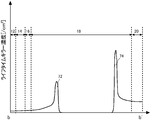
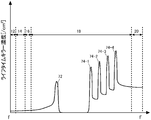
- FIG. 8 is a diagram showing an example of lifetime killer density distribution of the upper surface side lifetime control region 72 and the lower surface side lifetime control region 74 along the line bb ′ of FIG.
- helium ions are implanted from the upper surface 21 to form the upper surface side lifetime control region 72
- helium ions are implanted from the lower surface 23 to form the lower surface side lifetime control region 74.
- An example of the distribution is shown.
- the peak position (the depth in the Z-axis direction from the top surface 21) of the lifetime killer concentration of the top-side lifetime control area 72 is the Z-axis direction of the symbol “x” indicating the top-side lifetime control area 72 in FIG. Equal to the position in When helium ions are implanted from the upper surface 21, a lifetime killer having a concentration lower than the peak concentration may be distributed on the upper surface 21 side of the peak position.
- the peak position (the depth in the Z-axis direction from the lower surface 23) of the lifetime killer concentration of the lower surface-side lifetime control area 74 is the Z-axis direction of the symbol “x” indicating the lower surface side lifetime control area 74 in FIG. Equal to the position in When helium ions are implanted from the lower surface 23, a lifetime killer having a concentration lower than the peak concentration may be distributed closer to the lower surface 23 than the peak position.
- the peak concentration of the lifetime killer concentration of the lower surface side lifetime control region 74 may be higher or lower than the peak concentration of the lifetime killer concentration of the upper surface side lifetime control region 72.
- the peak concentration of the lifetime killer concentration of the lower surface side lifetime control region 74 is higher than the peak concentration of the lifetime killer concentration of the upper surface side lifetime control region 72.
- the lifetime killer concentration of the lower surface side lifetime control region 74 may be two to five times higher than the lifetime killer concentration of the upper surface side lifetime control region 72.
- the ordinate of the lifetime killer concentration distribution may be helium concentration, or may be the density of crystal defects formed by implantation of helium ions.
- the crystal defects may be interstitial helium, vacancies, double vacancies, and the like. These crystal defects form carrier recombination centers. Carrier recombination is promoted via the energy level (trap level) of the formed recombination center.
- the lifetime killer concentration corresponds to the trap level density.
- the lifetime killer concentration of the lower surface side lifetime control region 74 is higher than the lifetime killer concentration of the upper surface side lifetime control region 72. Therefore, in the semiconductor device 100 of this example, the carrier lifetime of the upper surface side lifetime control region 72 can be extended. Therefore, the semiconductor device 100 of this example can improve the leak current characteristic caused by the lifetime killer. Further, in the semiconductor device 100 of this example, the trade-off between the on voltage and the turn off loss of the transistor unit 70 can be made favorable.
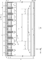
- FIG. 9 is a view showing another example of the aa ′ cross section in FIG.
- the semiconductor device 100 of FIG. 9 differs from the semiconductor device 100 of FIG. 2 in that a plurality of lower surface side lifetime control regions 74 are provided in the Z-axis direction.
- the semiconductor device 100 of FIG. 9 shows an example in which four lower surface side lifetime control regions 74 are provided in the Z-axis direction.
- the peak positions in the Z-axis direction of the lifetime killer concentration distribution of the lower surface side lifetime control region 74-1 to the lower surface side lifetime control region 74-4 are indicated by the symbol “x”.
- the lower surface side lifetime control area 74-4 provided on the lower surface 23 side is provided on the Y axis negative side than the lower surface side lifetime control area 74-1 provided on the upper surface 21 side. That is, as indicated by a broken line t-t 'in FIG. 9, the end of the lower surface side lifetime control area 74 is the end surface Klb1 of the lower surface side lifetime control area 74-1 to the lower surface side lifetime control area 74-4. It may be disposed on the Y axis negative side of FIG. The end Klb1 to the end Klb4 may be arranged in a straight line indicated by a broken line t-t 'in the YZ plane.
- the lower surface side lifetime control region 74-4 is provided on the Y axis negative side with respect to the upper surface side lifetime control region 72. Therefore, the semiconductor device 100 of this example can suppress the injection of holes from the emitter region 12 of the transistor unit 70 to the cathode region 82 of the diode unit 80 when the diode unit 80 operates. Therefore, the semiconductor device 100 of this example can improve the reverse recovery characteristic of the diode unit 80.
- the lengths in the Y-axis direction of the four lower surface side lifetime control areas 74 may be different from each other.
- the lower surface side lifetime control region 74-4 provided on the lower surface 23 side is provided on the Y axis negative side than the lower surface side lifetime control region 74-1 provided on the upper surface 21 side.
- the end of the lower surface side lifetime control region 74 is the lower surface side lifetime control region 74-4 from the end portion Krb1 of the lower surface side lifetime control region 74-1. It may be located on the Y axis negative side of FIG.
- the end Krb1 to the end Krb4 may be arranged in a straight line indicated by a broken line u-u 'in the YZ plane.
- the end on the Y-axis positive side of the lower surface side lifetime control region 74 is positioned on the Y-axis negative side as it extends from the end Klb1 to the end Klb4.
- the semiconductor device 100 of this example can suppress the injection of holes from the emitter region 12 of the transistor unit 70 to the cathode region 82 of the diode unit 80 when the diode unit 80 is operating.
- FIG. 10 is a view showing another example of the aa ′ cross section in FIG.
- the end Klb1 to the end Klb4 are arranged in a convex shape on the Y axis positive side in the YZ plane, This differs from the semiconductor device 100 of FIG.
- the end Klb2 and the end Klb3 are located on the positive side in the Y-axis direction.
- the end portion Krb1 to the end portion Krb4 are linearly arranged in the YZ plane, but may be arranged to be convex on the Y axis negative side, the Y axis positive side It may be arranged to have a convex shape.
- FIG. 11 shows the lifetime killer concentration distribution of the upper surface side lifetime control region 72 and the lower surface side lifetime control region 74-1 to the lower surface side lifetime control region 74-4 along the ff 'line of FIG. FIG.
- helium ions are injected from the lower surface 23, and an example of lifetime killer concentration distribution in the case where the lower surface side lifetime control region 74-1 to the lower surface side lifetime control region 74-4 are respectively formed is shown. ing.
- the peak position (the depth in the Z-axis direction from the lower surface 23) of the lifetime killer concentration of the lower surface-side lifetime control area 74 is the Z-axis direction of the symbol “x” indicating the lower surface side lifetime control area 74 in FIG. Equal to the position in When helium ions are implanted from the lower surface 23, a lifetime killer having a concentration lower than the peak concentration may be distributed closer to the lower surface 23 than the peak position.
- the lifetime killer concentration of the lower surface side lifetime control region 74-4 provided on the lower surface 23 side is the lifetime killer of the lower surface side lifetime control region 74-1 provided on the upper surface 21 side. It may be higher than the concentration.
- the lifetime killer concentration of the lower surface side lifetime control region 74-4 may be twice to five times as high as the lifetime killer concentration of the lower surface side lifetime control region 74-1.
- the lifetime killer concentration of the lower surface side lifetime control region 74 may be higher from the lower surface side lifetime control region 74-1 to the lower surface side lifetime control region 74-4.
- a valley may be formed between the peak concentrations of the two lower surface side lifetime control regions 74 adjacent to each other in the Z-axis direction to indicate the minimum of the lifetime killer concentration.
- the minimum value of the lifetime killer concentration in the valley on the lower surface 23 side may be higher than the minimum value of the lifetime killer concentration in the valley on the upper surface 21 side.
- the lifetime killer concentration from the position of the peak concentration in the lower surface side lifetime control region 74-4 to the position of the lower surface 23 is formed between two lower surface side lifetime control regions 74 adjacent in the Z-axis direction. It may be higher than the minimum value of lifetime killer concentration in any valley.
- the lifetime killer concentration of the lower surface side lifetime control region 74-4 provided on the lower surface 23 side is the lifetime of the lower surface side lifetime control region 74-1 provided on the upper surface 21 side. Higher than killer concentration. Therefore, in the semiconductor device 100 of this example, the lifetime killer concentration of the lower surface side lifetime control region 74-4 provided on the lower surface 23 side is the lower surface side lifetime control region 74-1 provided on the upper surface 21 side.
- the carrier lifetime of the upper surface side lifetime control area 72 can be made longer than when it is lower than the lifetime killer concentration. Therefore, the semiconductor device 100 of this example can improve the leak current characteristic caused by the lifetime killer. Further, in the semiconductor device 100 of this example, the trade-off between the on voltage and the turn off loss of the transistor unit 70 can be made favorable.
- the concentration of the lifetime killer only needs to be generally high from the upper surface 21 side to the lower surface 23 side. That is, the lifetime killer concentration is locally reversed in height, for example, the lifetime killer concentration of the lower surface side lifetime control region 74-2 is higher than the lifetime killer concentration of the lower surface side lifetime control region 74-3. It is also good.
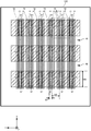
- FIG. 12 is a view showing an example of the semiconductor chip 98 according to the embodiment of the present invention.
- the transistor unit 70 and the diode unit 80 are alternately and periodically arranged in the XY plane.
- FIG. 12 shows an example in which two transistor portions 70 are provided in the X axis direction and five in the Y axis direction, and two diode portions 80 are provided in the X axis direction and six in the Y axis direction.
- FIG. 1 is an enlarged view of the area S of FIG.
- the upper surface side lifetime control area 72 is provided in the area of the broken line in FIG.
- the upper surface side lifetime control region 72 may be provided to include the cathode region 82 of the diode section 80 in the XY plane, as shown in FIG.
- the lower surface side lifetime control area 74 is provided in the area of the dashed dotted line in FIG.
- the lower surface side lifetime control region 74 may be provided from the transistor unit 70 to the diode unit 80.
- the cathode region 82 of the diode section 80 is provided in the depth direction of the semiconductor chip 98 in the top view of FIG. 12.
- the width WI is the width in the Y-axis direction of the transistor portion 70. Further, the width WF is the width in the Y-axis direction of the diode unit 80. The width WI may be larger than the width WF. The width WI may be at least twice and at most 5 times the width WF. The width WI is, for example, 1500 ⁇ m. The width WF is 500 ⁇ m as an example.
- the lower surface side lifetime control region 74 may be provided up to a region E which is outside the upper surface side lifetime control region 72 in the X-axis direction, as shown in FIG. That is, the lower surface side lifetime control region 74 may be provided from the upper surface side lifetime control region 72 to both ends of the semiconductor chip 98 along the X axis.
- FIG. 13 is an enlarged view of a region F in FIG.
- the distance B is a distance from the end Kls to the boundary between the transistor unit 70 and the diode unit 80 in the Y-axis direction.
- the distance C is a distance between the boundary between the transistor unit 70 and the diode unit 80 and the end Klb in the Y-axis direction.
- the distance B may be equal to or greater than 0.01 times and equal to or less than 0.15 times the width WI of the transistor portion 70. Further, the distance C may be not less than 0.015 times and not more than 0.03 times the width WF of the diode section 80.
- the distance A is a distance between the end Kls and the end Klb in the Y-axis direction.
- FIG. 14 is a view showing an example of the gg ′ cross section in FIG.
- the upper surface side lifetime control region 72 is provided from the transistor unit 70 through the diode unit 80 to the transistor unit 70 adjacent to the diode unit 80 on the opposite side in the Y-axis direction.
- the lower surface side lifetime control region 74-1 to the lower surface side lifetime control region 74-4 are formed from each of the transistor portions 70 adjacent on both sides of the diode portion 80 in the Y-axis direction.
- the diode unit 80 is provided.
- the distance D is between the end Klb4 of the lower surface side lifetime control area 74-4 on the Y axis positive side and the end Krb4 of the lower surface side lifetime control area 74-4 on the Y axis negative side in the Y axis direction. Distance.
- the ratio of the distance D to the width WF of the diode unit 80 may be 95% or more and 99% or less.
- the upper surface side lifetime control region 72 is provided from the transistor unit 70 on the Y-axis positive side to the transistor unit 70 on the Y-axis negative side via the diode unit 80.
- the length Ls is a length between the end Kls and the end Krs.
- the length Ls may be larger than the thickness T of the semiconductor substrate 10. By making the length Ls larger than the thickness T, holes generated in the drift region 18 are likely to recombine with electrons. Therefore, the semiconductor device 100 of this example can suppress the switching loss of the transistor unit 70.
- FIG. 15 is a view showing another example of the gg ′ cross section in FIG.
- the semiconductor device 100 of this example is the semiconductor of FIG. 14 in that the lower surface side lifetime control region 74-1 to the lower surface side lifetime control region 74-4 are provided in the entire diode section 80 in the Y-axis direction. It differs from the device 100.
- the lower surface side lifetime control region 74-1 to the lower surface side lifetime control region 74-4 may be provided in the entire Y-axis direction of the diode section 80.
- FIG. 16 is a view showing another example of the gg ′ cross section in FIG.
- the lifetime killer concentration of the lower surface side lifetime control region 74-1 to the lower surface side lifetime control region 74-4 at the boundary between the transistor portion 70 and the diode portion 80 is the lower surface other than the boundary.
- This embodiment differs from the semiconductor device 100 of FIG. 15 in that it is higher than the lifetime killer concentration of the side lifetime control area 74-1 to the lower surface side lifetime control area 74-4.
- the boundary between the transistor portion 70 and the diode portion 80 is indicated by a region U and a region U '.
- the lifetime killer density of the lower surface side lifetime control region 74-1 to the lower surface side lifetime control region 74-4 in the region U and the region U ′ is higher than that in the regions U and U ′. Therefore, in the semiconductor device 100 of the present example, injection of holes from the emitter region 12 of the transistor unit 70 to the cathode region 82 of the diode unit 80 during operation of the diode unit 80 is higher than that of the semiconductor device 100 of FIG. It can suppress more. Therefore, the semiconductor device 100 of this example can further improve the reverse recovery characteristic of the diode unit 80. It should be noted that there is a region where the lower surface side lifetime control region 74-1 to the lower surface side lifetime control region 74-4 are not partially provided in regions other than the region U and the region U ′ in the Y axis direction. May be
- FIG. 17 is a view showing an example of lifetime killer concentration distribution in the Y-axis direction of the lower surface side lifetime control region 74-4 along the line hh ′ in FIG. 15 and the line jj ′ in FIG. is there.
- the lifetime killer concentration of the lower surface side lifetime control region 74-4 in the jj 'cross section is locally high in the region U and the region U'.
- the lifetime killer concentration of the lower surface side lifetime control region 74-4 in the jj ′ cross section is the lifetime killer concentration of the lower surface side lifetime control region 74-4 in the hh ′ cross section It may be 2 to 5 times higher.
- the lifetime killer concentration of the lower surface side lifetime control region 74 is locally high in the regions U and U ′. Therefore, compared with the example of FIG. 15, the semiconductor device 100 of this example can further suppress the injection of holes from the emitter region 12 of the transistor unit 70 to the diode unit 80 when the diode unit 80 operates. Therefore, the semiconductor device 100 of this example can further improve the reverse recovery characteristic of the diode unit 80 as compared with the example of FIG.
- the lifetime killer concentrations of the lower surface side lifetime control region 74-1 in the region U and the region U ′ may be different from each other. Further, the lifetime killer concentration of any of the lower surface side lifetime control region 74-1 to the lower surface side lifetime control region 74-4 may be locally high in the regions U and U '.
- FIG. 18 is a view partially showing an example of the upper surface of another semiconductor device 200 according to this embodiment.
- the semiconductor device 200 shown in FIG. 18 differs from the semiconductor device 100 shown in FIG. 1 in that the floating region 17 of the second conductivity type is provided below the upper surface 21 of the diode section 80.
- Floating region 17 is, for example, of P + type.
- the floating region 17 may be provided at a predetermined distance on the X axis positive side from the end on the X axis negative side of the cathode region 82 in a top view of the semiconductor substrate 10 as shown in FIG.
- the floating region 17 may be provided at a predetermined distance on the Y axis negative side from the end on the Y axis positive side of the cathode region 82 in a top view of the semiconductor substrate 10.
- a plurality of floating regions 17 may be provided in the Y-axis direction in a top view of the semiconductor substrate 10. Although one floating region 17 is illustrated in the X-axis direction in FIG. 18, the region from the region adjacent to the X-axis negative side end of the cathode region 82 to the region adjacent to the X-axis positive side end Plural, in the X-axis direction may be provided. The floating region 17 may be provided inside the cathode region 82 in top view.
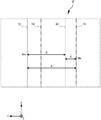
- FIG. 19 is an enlarged view of a region G in FIG.
- the width Wfl1 is the width in the Y-axis direction of the floating region 17, and the width Wfl2 is the width in the X-axis direction of the floating region 17.
- the width Wff1 is a distance between the floating region 17 and another floating region 17 adjacent to the floating region in the Y-axis direction.
- the width Wm is a mesa width of the diode mesa portion 64.
- a plurality of other floating regions 17 may be provided adjacent to the floating region 17 on the X-axis positive side of the floating region 17 shown in FIG. 19 at predetermined intervals.
- the width Wfl1 may be smaller than the width Wm.
- the width Wfl2 may be smaller than the width Wm.
- the width Wff1 may be smaller than the width Wfl1.
- the width Wff1 may be smaller than the width Wfl2.
- FIG. 20 is a view showing an example of a qq 'cross section in FIG.
- the floating region 17 is provided on the lower surface 23 side in the diode section 80.
- the floating region 17 may be provided above the buffer region 20.
- the floating region 17 may be provided in contact with the buffer region 20.
- Floating region 17 is a region in an electrically floating state.
- the electrically floating state indicates a state in which the collector electrode 24 and the emitter electrode 52 are not electrically connected.
- a plurality of floating regions 17 may be provided in the Y-axis direction. Further, a plurality of floating regions 17 may be provided on the X axis positive side of floating region 17 shown in FIG. In the Z-axis direction, floating region 17 may be provided closer to lower surface 23 than lower surface side lifetime control region 74. At least a portion of the floating region 17 may overlap with the lower surface side lifetime control region 74 provided in a portion of the diode section 80 in top view.
- FIG. 20 shows an example in which the floating area 17 provided on the most positive side in the Y-axis direction overlaps the lower surface side lifetime control area 74 in top view, but at least a part of the floating area 17 is viewed from above And may overlap the lower surface side lifetime control area 74.
- the at least one floating region 17 may not overlap with the lower surface side lifetime control region 74 in the Y-axis direction.
- FIG. 20 shows an example in which the floating area 17 excluding the floating area 17 provided on the most positive side in the Y-axis direction does not overlap the lower surface side lifetime control area 74 in the Y-axis direction.
- the distance Ds is a distance from the upper surface 21 of the upper surface side lifetime control area 72 in the Z-axis direction.
- the distance Db is a distance from the lower surface 23 of the lower surface side lifetime control area 74 in the Z-axis direction. Both of the distance Ds and the distance Db may be smaller than half of the thickness T of the semiconductor substrate 10.
- the distance Db may be smaller than the distance Ds.
- the distance Ds may be 10 ⁇ m to 30 ⁇ m.
- the distance Ds is 17 ⁇ m as an example.
- the distance Db may be 5 ⁇ m or more and 20 ⁇ m or less.
- the distance Db is, for example, 10 ⁇ m.
- FIG. 21 is a view showing the qq 'cross section shown in FIG. 20 including the transistor section 70 adjacent on the Y axis negative side of the diode section 80.
- a plurality of floating regions 17 are provided in the diode unit 80 at intervals Wff1 in the Y-axis direction.
- the floating region 17 provided on the most positive side in the Y-axis direction may be provided adjacent to the boundary between the diode unit 80 and the transistor unit 70 adjacent on the Y-axis positive side.
- the floating region 17 provided on the most negative side in the Y-axis direction may be provided adjacent to the boundary between the diode unit 80 and the adjacent transistor unit 70 on the Y-axis negative side.
- the semiconductor device 200 of this example since the floating region 17 is provided in the diode unit 80, injection of electrons from the cathode region 82 can be suppressed. Therefore, the semiconductor device 200 of this example can suppress the surge voltage of the diode unit 80.
- the sum of the widths Wfl1 of the floating regions 17 from the floating region 17 provided on the most positive side in the Y-axis direction to the floating region 17 provided on the most negative side is greater than the width WF in the Y-axis direction of the diode section 80 It may be small. That is, the floating region 17 may cover a portion of the cathode region 82 above the cathode region 82. In other words, a part of the cathode region 82 in the Y-axis direction may not be covered by the floating region 17. In this example, in the semiconductor device 200, a part of the cathode region 82 in the Y-axis direction is not covered by the floating region 17, so that the diode unit 80 can perform diode operation.
- the sum of the widths Wfl1 of the floating regions 17 from the floating region 17 provided on the most positive side in the Y-axis direction to the floating region 17 provided on the most negative side is 65 of the width WF of the diode section 80 in the Y-axis direction. % Or more and 95% or less. More preferably, the sum may be 75% or more and 85% or less of the width WF. In the semiconductor device 200 of this example, since the sum is 65% or more and 95% or less of the width WF, the diode portion 80 can perform diode operation while suppressing the surge voltage of the diode portion 80.
- the distance D is the distance from the end on the Y-axis negative side of the bottom-side lifetime control area 74 on the Y-axis positive side to the end on the Y-axis positive side of the bottom-side lifetime control area 74 on the Y-axis negative side. is there. That is, the distance D is the width in the Y-axis direction of the area where the lower surface side lifetime control area 74 is not provided in the diode section 80.
- the distance D may be larger than the sum of the widths Wfl1 of the floating regions 17 from the floating region 17 provided on the most positive side in the Y-axis direction to the floating region 17 provided on the most negative side.
- the distance D may be 95% or more and 99% or less of the width WF of the diode unit 80 in the Y-axis direction. More preferably, the distance D may be 96% or more and 98% or less of the width WF. That is, the area where the lower surface side lifetime control area 74 is provided may be 1% to 5%, and more preferably 2% to 4%, of the width WF in the Y-axis direction. In the semiconductor device 200 of this example, since the floating region 17 is provided in the diode unit 80, carrier distribution in the depth direction of the semiconductor substrate 10 can be adjusted in the diode unit 80.
- the semiconductor device 200 of the present example since the lower surface side lifetime control region 74 is provided in the transistor portion 70, the holes of the minority carriers generated in the drift region 18 offset the electrons of the majority carrier with a short lifetime. It will be easier. Therefore, the semiconductor device 200 of this example can improve the leak current characteristics of the transistor unit 70. Further, in the semiconductor device 200 of this example, the trade-off between the on-state voltage and the turn-off loss of the transistor unit 70 can be made favorable.
- FIG. 22 is a view showing an example of the upper surface of the semiconductor chip 120 according to the present embodiment.
- the transistor units 70 and the diode units 80 are periodically and alternately arranged in the XY plane.
- FIG. 22 shows an example in which three transistor portions 70 are provided in the X-axis direction and seven in the Y-axis direction, and three diode portions 80 are provided in the X-axis direction and six in the Y-axis direction.
- the dividing unit 46 may be provided.
- the dividing unit 46 may be provided with a gate runner 48 that supplies a gate voltage to the transistor unit 70.
- the width WI is the width in the Y-axis direction of the transistor portion 70.
- the width WF is the width in the Y-axis direction of the diode section 80.
- the width Wh is a width from the end of the well region 11 on the X-axis positive side to the end of the well region 11 on the X-axis negative side, as described later.
- the width is equal to the width of the portion where the base region 14 is provided on the upper surface 21 side of the semiconductor substrate 10 and the well region 11 is not provided.
- the contact region 15 and the emitter region 12 are provided in the region indicated by the width Wh so as to be exposed to the upper surface 21.
- the contact region 15 and the base region 14 are provided in the region indicated by the width Wh so as to be exposed to the upper surface 21.
- the transistor units 70 may be disposed at both ends on the outer circumferential side in the arrangement direction of the transistor unit 70 and the diode unit 80 (Y-axis direction).
- the transistor portion 70 may face the edge termination portion.
- An upper surface side lifetime control region 72 and a lower surface side lifetime control region 74 are provided in the semiconductor chip 120 of this example.
- the range in which the upper surface side lifetime control area 72 and the lower surface side lifetime control area 74 are provided in the upper surface view is indicated by hatched portions.
- the upper surface side lifetime control region 72 and the lower surface side lifetime control region 74 are continuously provided in the X-axis direction across the dividing portion 46 from the edge terminal end on the X-axis positive side to the edge terminal end on the X-axis negative side. It may be done.
- the upper surface side lifetime control region 72 is the Y axis of the transistor portion 70 adjacent on the Y axis negative side of the diode portion 80 from a part of the transistor portion 70 adjacent on the Y axis positive side of the diode portion 80 in the Y axis direction. It may be provided continuously in the Y-axis direction up to a part in the direction. That is, the upper surface side lifetime control region 72 is a transistor adjacent on the Y axis negative side from the transistor portion 70 adjacent on the Y axis positive side of the diode portion 80 so as to cover the entire diode portion 80 in the Y axis direction. It may be provided continuously to the part 70 in the Y-axis direction. The upper surface side lifetime control region 72 may not be provided at the central portion of the transistor unit 70 in the Y-axis direction.
- the lower surface side lifetime control region 74 may be provided continuously in the Y-axis direction from the region adjacent to the diode unit 80 in the transistor unit 70 to the region adjacent to the transistor unit 70 in the diode unit 80. . That is, the lower surface side lifetime control region 74 may be provided continuously in the Y-axis direction from the transistor unit 70 to the diode unit 80 across the boundary between the transistor unit 70 and the diode unit 80.
- the lower surface side lifetime killer may not be provided at the central portion of the diode unit 80 in the Y-axis direction.
- the lower surface side lifetime control region 74 provided in the overlapping region may be another lower surface side lifetime control region 74.
- FIG. 23 is an enlarged view of a region A1 in FIG.
- FIG. 23 is a diagram showing the configuration of the cathode region 82 and the floating region 17 in the diode section 80. As shown in FIG. In FIG. 23, configurations other than the cathode region 82 and the floating region 17 such as the gate trench portion 40 and the dummy trench portion 30 provided in the diode portion 80 and the transistor portion 70 are omitted.
- the semiconductor device 300 of this example in the diode section 80, ten floating regions 17 are provided in the X axis direction and two in the Y axis direction inside the cathode region 82 in the XY plane. Further, in the semiconductor device 300 of this example, the end portion S of the P + -type well region 11 is provided on the X axis positive side of the diode unit 80 and the transistor unit 70. Further, in the semiconductor device 300 of this example, the end S ′ of the P + -type well region 11 is provided on the X axis negative side of the diode unit 80 and the transistor unit 70. In the present example, the well region 11 is provided outside the region where the transistor section 70 and the diode section 80 are alternately arranged. In other words, in the present example, the well region 11 is not provided in the region inside the transistor portion 70 and the diode portion 80 rather than the end portion S.
- a transistor unit 70 is provided adjacent to the diode unit 80 on both the Y-axis positive side and the Y-axis negative side of the diode unit 80.
- the width WI of the transistor unit 70 in the Y-axis direction may be larger than the width WF of the diode unit 80 in the Y-axis direction.
- the width WI may be at least twice and at most 5 times the width WF.
- the width WI may be in the range of 1200 ⁇ m to 2000 ⁇ m.
- the width WI is, for example, 1500 ⁇ m.
- the width WF may be 400 ⁇ m or more and 600 ⁇ m or less.
- the width WF is 500 ⁇ m as an example.
- the width Wh from the end S of the well region 11 on the X axis positive side to the end S ′ of the well region 11 on the X axis negative side may be larger than the width WI.
- the width Wh may be 1.5 times or more and 3 times or less the width WI.
- the width Wh may be in the range of 3000 ⁇ m to 3600 ⁇ m.
- the width Wh is, for example, 3100 ⁇ m.
- the width Wh may be larger than the sum of the width WI and the width WF.
- the semiconductor device 300 of this example suppresses the snapback phenomenon when the transistor portion 70 is turned on or when the diode portion 80 is turned on because the width Wh is larger than the sum of the width WI and the width WF. it can.
- the snapback phenomenon is a phenomenon in which the voltage between the collector electrode 24 and the emitter electrode 52 sharply decreases with an increase in the current flowing between the collector electrode 24 and the emitter electrode 52.
- the upper surface side lifetime control region 72 is a portion of the transistor portion 70 adjacent on the Y-axis positive side of the diode portion 80 in the Y-axis direction on the Y-axis negative side of the diode portion 80. It is provided continuously in the Y-axis direction up to a part of the adjacent transistor portions 70 in the Y-axis direction.
- the upper surface side lifetime control region 72 is continuously provided in the X axis direction from the well region 11 provided on the X axis positive side of the transistor unit 70 and the diode unit 80 to the well region 11 provided on the X axis negative side. Good.
- the area where the upper surface side lifetime control area is provided is indicated by the hatched portion.
- the upper surface side lifetime control region 72 may not be provided in part of the transistor unit 70 in the Y-axis direction.
- the length Ls is a length of the upper surface side lifetime control area 72 in the Y-axis direction.
- the distance B is a distance from the boundary between the diode unit 80 and the transistor unit 70 adjacent on the Y-axis positive side to the end of the upper surface side lifetime control region 72 on the Y-axis positive side.
- the distance B is the distance from the boundary between the diode unit 80 and the transistor unit 70 adjacent to the Y-axis negative side to the end of the upper surface side lifetime control region 72 on the Y-axis negative side.
- the lower surface side lifetime control region 74 extends from the region adjacent to the diode unit 80 in the transistor unit 70 to the region adjacent to the transistor unit 70 in the diode unit 80 in the Y-axis direction. It is provided continuously to That is, in the present example, the lower surface side lifetime control region 74 is provided continuously in the Y-axis direction from the transistor unit 70 to the diode unit 80 across the boundary between the transistor unit 70 and the diode unit 80.
- the length Lb is a length of the lower surface side lifetime control area 74 in the Y-axis direction.
- the lower surface side lifetime killer is not provided at the central portion of the diode unit 80 in the Y-axis direction. Further, in the present embodiment, in the top view of the semiconductor substrate 10, the region overlapping the boundary between the diode unit 80 and the transistor unit 70 adjacent on the Y-axis positive side and the boundary between the transistor unit 70 adjacent on the Y-axis negative side.
- the lower surface side lifetime control area 74 is provided in each of the overlapping areas.
- the lower surface side lifetime control region 74 may be provided to overlap a part of the floating region 17 in the Y-axis direction on the boundary side between the transistor unit 70 and the diode unit 80 in a top view.
- the distance C is a distance from the boundary between the transistor unit 70 adjacent on the Y-axis positive side of the diode unit 80 and the end on the Y-axis negative side of the lower surface side lifetime control region 74. Further, the distance C is a distance from the boundary between the transistor unit 70 adjacent on the Y-axis negative side of the diode unit 80 and the end on the Y-axis positive side of the lower surface side lifetime control region 74.
- Distance D is the Y-axis direction from the end on the Y-axis negative side of the bottom-side lifetime control area 74 on the Y-axis positive side to the end on the Y-axis positive side of the bottom-side lifetime control area 74 on the Y-axis negative side Is the distance at The distance A is a distance in the Y-axis direction from the end on the Y-axis positive side of the bottom-side lifetime control area 74 on the Y-axis positive side to the end on the Y-axis positive side of the top-surface lifetime control area 72.
- the distance A may be smaller than the distance B. That is, in the transistor unit 70, the lower surface side lifetime control region 74 may be disposed closer to the diode portion 80 than the upper surface side lifetime control region 72.
- the semiconductor device 300 of this example since the distance A is smaller than the distance B, injection of holes from the emitter region 12 of the transistor unit 70 to the cathode region 82 of the diode unit 80 can be suppressed when the diode unit 80 operates. Therefore, the semiconductor device 300 of this example can improve the reverse recovery characteristic of the diode unit 80.
- the distance A may be 0.25 times or more and 0.5 times or less the distance B.
- the distance A may be 50 ⁇ m to 100 ⁇ m.
- the length Lb may be longer than the distance C. That is, the lower surface side lifetime control region 74 provided on the transistor portion 70 side from the boundary is lower than the lower surface side lifetime control region 74 provided on the diode portion 80 side from the boundary between the transistor portion 70 and the diode portion 80 , Y axis direction may be long.
- the semiconductor device 300 of this example since the length Lb is longer than the distance C, the injection of holes from the emitter region 12 of the transistor unit 70 to the cathode region 82 of the diode unit 80 can be suppressed when the diode unit 80 operates. . Therefore, the semiconductor device 300 of this example can improve the reverse recovery characteristic of the diode unit 80.
- FIG. 24 is an enlarged view of a region B1 in FIG.
- FIG. 24 is an enlarged view from the end S of the well region 11 on the X axis positive side of the diode section 80 in FIG. 23 to the end S ′ of the well region 11 on the X axis negative side.
- ten floating regions 17 are provided in the X axis direction and two in the Y axis direction inside the cathode region 82 in the XY plane.
- the width Wwc is the width in the X-axis direction from the end S of the well region 11 on the X-axis positive side to the end of the cathode region 82 on the X-axis positive side.
- the width Wwc is the width in the X-axis direction from the end S ′ of the well region 11 on the X-axis negative side to the end of the cathode region 82 on the X-axis negative side.
- the width Wwc may be smaller than the width WF of the diode unit 80.
- the width Wwc may be not less than 0.25 times and not more than 0.75 times the width WF.
- the width Wwc may be 150 ⁇ m or more and 300 ⁇ m or less.
- the width Wwc is, for example, 250 ⁇ m.
- a plurality of contact holes 54 are provided side by side in the Y-axis direction. Although one contact hole 54 is shown in FIG. 24, in fact, as apparent from the top views shown in FIGS. 1 and 18, the position in the X-axis direction is the end of the contact hole 54.
- a plurality of contact holes 54 equal to the position of T and equal to the position of the end T ′ of the contact hole 54 are provided in the Y-axis direction.
- the width Wwca is a width in the X-axis direction between the end S on the X-axis positive side of the well region 11 and the end T on the X-axis positive side of the contact hole 54.
- the width Wwca is the width in the X-axis direction between the end S ′ on the X-axis negative side of the well region 11 and the end T ′ on the X-axis negative side of the contact hole 54.
- the end T on the X-axis positive side of the contact hole 54 is provided away from the end S on the X-axis positive side of the well region 11 by a width Wwca on the X-axis negative side.
- the end T ′ on the X axis negative side of the contact hole 54 is provided away from the end S ′ on the X axis negative side of the well region 11 by a width Wwca on the X axis positive side.
- the contact hole 54 may be provided continuously in the X-axis direction from the end T to the end T ′.
- the width Wwcb is a width in the X-axis direction between the end T of the contact hole 54 and the end of the cathode region 82 on the X-axis positive side.
- the width Wwcb is the width in the X-axis direction between the end T ′ of the contact hole 54 and the end of the cathode region 82 on the X-axis negative side.
- the width Wwca may be smaller than the width Wwcb.
- the width Wwca may be not less than 0.1 times and not more than 0.9 times the width Wwcb.
- the width Wwca may be not less than 20 ⁇ m and not more than 110 ⁇ m.
- the width Wwcb may be 120 ⁇ m or more and 180 ⁇ m or less.
- the width Wwca is, for example, 100 ⁇ m.
- the width Wwcb is, for example, 150 ⁇ m.
- the sum of the width Wwca and the width Wwcb is the width Wwc.
- a floating region 17 is provided inside of the cathode region 82 in the XY plane. Floating region 17 is not electrically connected to any of collector electrode 24 and emitter electrode 52.
- the floating regions 17 are provided in a lattice shape in the XY plane.
- the lattice shape refers to a state in which the floating regions 17 are periodically arranged in both the X-axis direction and the Y-axis direction.
- two floating regions 17 are provided in the Y-axis direction, and ten floating regions 17 are provided in the X-axis direction.
- the opening region 85 is a region between two floating regions 17 provided adjacent to each other in the X-axis direction in the X-axis direction. Further, the opening area 85 is an area between two floating areas 17 provided adjacent to each other in the Y-axis direction in the Y-axis direction. In the present example, ten floating regions 17 are provided across the opening region 85 from the X-axis negative side of the cathode region 82 to the X-axis positive side.
- the width Wff2 is the width in the X-axis direction of the opening region 85.
- the width Wff2 is smaller than the width Wfl2 of the floating region 17 in the X-axis direction.
- the width Wff2 may be smaller than the width WF of the diode unit 80.
- the width Wff2 may be not less than 0.01 times and not more than 0.05 times the width WF.
- the width Wff2 may be 6 ⁇ m or more and 20 ⁇ m or less.
- the width Wff2 is 10 ⁇ m as an example.
- the width Wfl2 of the floating region 17 in the X-axis direction may be smaller than the width WF of the diode section 80.
- the width Wfl2 may be not less than 0.25 times and not more than 0.75 times the width WF.
- the width Wfl2 may be 150 ⁇ m or more and 300 ⁇ m or less.
- the width Wfl2 is 240 ⁇ m as an example.
- the width Wfl1 of the floating region 17 in the Y-axis direction may be smaller than the width WF of the diode section 80.
- the width Wfl1 may be not less than 0.25 times and not more than 0.75 times the width WF.
- the width Wfl1 may be 150 ⁇ m or more and 300 ⁇ m or less.
- the width Wfl1 may be equal to or different from the width Wfl2.
- the width Wfl1 is 240 ⁇ m as an example.
- the width Wcf2 is a width in the X-axis direction between the X-axis positive end of the cathode region 82 and the X-axis positive end of the floating region 17 disposed on the most positive side in the X-axis direction.
- the width Wcf2 may be smaller than the width Wff2.
- the width Wcf2 may be not less than 0.1 times and not more than 0.9 times the width Wff2.
- the width Wcf2 may not be zero.
- the width Wcf2 may be 2 ⁇ m or more and 6 ⁇ m or less.
- the width Wcf2 is 5 ⁇ m as an example.
- the width in the X-axis direction between the X-axis negative side end of the cathode region 82 and the X-axis negative side end of the floating region 17 disposed on the most negative side in the X-axis direction is also equal to the width Wcf2.
- the width Wff1 is the width in the Y-axis direction of the opening region 85.
- the width Wff1 may be smaller than the width Wfl1.
- the width Wff1 may be smaller than the width WF of the diode unit 80.
- the width Wff1 may be not less than 0.01 times and not more than 0.05 times the width WF of the diode section 80.
- the width Wff1 may be 6 ⁇ m or more and 20 ⁇ m or less.
- the width Wff1 may be equal to or different from the width Wff2.
- the width Wff1 is 10 ⁇ m as an example.
- the total area of the plurality of floating regions 17 disposed inside the cathode region 82 in the XY plane may be smaller than the area of the cathode region 82 in the XY plane.
- the total area of the plurality of floating regions 17 in the XY plane may be 50% or more and 99% or less of the area of the cathode region 82 in the XY plane.
- Wh is 3100 ⁇ m
- Wwc is 250 ⁇ m
- Wfl2 and Wfl1 are 240 ⁇ m
- Wcf2 and Wcf1 are 5 ⁇ m
- Wff2 and Wff1 are 10 ⁇ m
- the plurality of floating regions 17 occupy the area of cathode region 82 in the XY plane.
- the total area is 88.6%. That is, a part of the cathode region 82 may not be covered by the floating region 17. In the semiconductor device 300 of this example, since the cathode region 82 is not partially covered by the floating region 17, the diode unit 80 can perform diode operation.
- the width Wcf1 is a width from the end on the Y-axis positive side of the cathode region 82 to the end on the Y-axis positive side of the floating region 17 on the Y-axis positive side.
- the width Wcf1 is the width from the end on the Y axis negative side of the cathode region 82 to the end on the Y axis negative side of the floating region 17 on the Y axis negative side.
- the width Wcf1 may be smaller than the width WF of the diode unit 80.
- the width Wcf1 may be not less than 0.01 times and not more than 0.05 times the width WF.
- the width Wcf1 may not be zero. Further, the width Wcf1 may be equal to or different from the width Wcf2.
- the width Wcf1 may be 2 ⁇ m or more and 6 ⁇ m or less.
- the width Wcf1 is 5 ⁇ m as an example.
- the width Wcnt is a width in the arrangement direction (Y-axis direction) of the contact holes 54.
- the width Wcnt may be smaller than Wff2.
- the width Wcnt may be smaller than Wff1.
- the width Wcnt may be smaller than Wcf2.
- the width Wcnt may be smaller than Wcf1.
- the width Wcnt may be 0.3 ⁇ m or more and 0.7 ⁇ m or less.
- the width Wcnt is 0.5 ⁇ m as an example.
- the upper surface side lifetime control region 72 is provided on the entire surface of the region B1 in top view.
- the lower surface side lifetime control area 74 is continuously provided from the X axis positive side of the area B in the X axis direction to the negative side.
- the lower surface side lifetime control region 74 includes a region overlapping the boundary between the diode unit 80 and the transistor unit 70 adjacent to the diode unit 80 on the Y-axis positive side and the transistor unit 70 adjacent on the Y-axis negative side. It is provided in the area
- the lower surface side lifetime control region 74 is not provided at the central portion of the diode portion 80 in the Y-axis direction.
- the distance C is a distance from the boundary between the transistor unit 70 adjacent on the Y-axis positive side of the diode unit 80 and the end on the Y-axis negative side of the lower surface side lifetime control region 74. Further, the distance C is a distance from the boundary between the transistor unit 70 adjacent on the Y-axis negative side of the diode unit 80 and the end on the Y-axis positive side of the lower surface side lifetime control region 74.
- Distance D is the Y-axis direction from the end on the Y-axis negative side of the bottom-side lifetime control area 74 on the Y-axis positive side to the end on the Y-axis positive side of the bottom-side lifetime control area 74 on the Y-axis negative side Is the distance at That is, the distance D is the width of the area where the lower surface side lifetime control area 74 is not provided in the Y-axis direction.
- FIG. 25 is an enlarged view of a region B2 in FIG.
- the width Wcf2 is a width in the X-axis direction between an end on the X-axis positive side of the cathode region 82 and an end on the X-axis positive side of the floating region 17 disposed on the most positive side in the X-axis direction. It is.
- the width Wcf1 is the width in the Y-axis direction between the end on the Y-axis positive side of the cathode region 82 and the end on the Y-axis positive side of the floating region 17 on the Y-axis positive side.
- the width Wcf1 is 5 ⁇ m as an example.
- the width Wff2 is the width in the X-axis direction of the opening region 85.
- the width Wfl2 is the width of the floating region 17 in the X-axis direction.
- the width Wcf2 may be smaller than the width Wfl2.
- injection of electrons from the cathode region 82 can be suppressed at the end of the diode section 80.
- the distance C is a distance in the Y-axis direction between the boundary between the diode unit 80 and the transistor unit 70 adjacent on the Y-axis positive side and the end of the lower surface side lifetime control region 74 on the Y-axis negative side.
- FIG. 26 is a view showing an example of the h-h 'cross section in FIG.
- the high-concentration region 19 of the first conductivity type may be provided below the base region 14 provided on the upper surface 21.
- the high concentration region 19 of this example is, for example, an N + -type.
- the high concentration region 19 may not be provided in the diode unit 80.
- a plurality of high concentration regions 19 may be provided in the Z-axis direction.
- two high concentration regions 19 are provided, ie, a high concentration region 19-1 and a high concentration region 19-2.
- An N-type region is provided between the high concentration region 19-1 and the high concentration region 19-2 in the Z-axis direction.
- the doping concentration in the N-type region may be lower than the high concentration region 19-1 and the high concentration region 19-2.
- the doping concentration in the N-type region may be equal to the doping concentration of the drift region 18 or higher than the doping concentration of the drift region 18.
- the concentration of holes decreases due to the charge neutral condition, as compared with the drift region 18. That is, the high concentration region 19 suppresses the injection of holes from the base region 14 to the drift region 18. Therefore, the semiconductor device 300 of this example can significantly reduce the injection efficiency of minority carriers from the base region 14 to the drift region 18.
- the minority carrier injection efficiency is reduced as the number of high concentration regions 19 increases. Therefore, as the number of high concentration regions 19 increases, the reverse recovery characteristics of the diode unit 80, particularly the recovery current, is significantly reduced.
- the floating region 17 is provided in the buffer region 20 provided above the cathode region 82 in the diode unit 80.
- two floating regions 17 are provided in the Y-axis direction in the h-h 'cross section.
- boundary position P1 is a boundary position on the Y axis positive side.
- boundary position P1 ′ is a boundary position on the Y axis negative side.
- Boundary positions P1 and P1 ′ are boundary positions in a cross section parallel to the h ⁇ h ′ cross section.
- the hh ′ cross section is a plane perpendicular to the lower surface 23 and parallel to the arrangement direction of the dummy trench portions 30.
- the end position P2 is a position in the Y-axis direction of the end closest to the boundary position P1 of the floating region 17 disposed on the Y-axis positive side. Further, the end position P2 'is a position in the Y axis direction of the end closest to the boundary position P1' of the floating region 17 disposed on the Y axis negative side.
- a plurality of floating regions 17 may be provided in the Y-axis direction from the end position P2 to the end position P2 ′. In this example, two floating regions 17 are provided in the Y-axis direction from the end position P2 to the end position P2 ′.
- the opening region 85 in which the floating region 17 is not provided is present at the depth position substantially the same as the floating region 17 in the Z-axis direction.
- the open area 85 may refer to an area sandwiched by the floating area 17 in the Y-axis direction.
- the open area 85 is an N + -type area.
- the doping concentration of the opening region 85 may be substantially the same as the doping concentration of the drift region 18 or the buffer region 20.
- the open area 85 may be the drift area 18 or the buffer area 20 remaining without forming the floating area 17.
- the width Wcf1 is a width from the end position P1 to the end position P2.
- the width Wcf1 is a width from the end position P1 ′ to the end position P2 ′.
- the width Wff1 is an interval between two floating regions 17 adjacent to each other across the opening region 85 in the Y-axis direction.
- the width Wcf1 may be smaller than the width Wff1.
- the width Wcf1 may be half or less of the width Wff1 or may be 1/4 or less.
- the width Wcf1 may not be zero. In the semiconductor device 300 of this example, since the width Wcf1 is small, the injection of electrons from the cathode region 82 can be suppressed at the end of the diode unit 80.
- the width Wd is the width in the Z-axis direction of the floating region 17.
- the width Wd may be smaller than the width Wcf1.
- the width Wd may be not less than 0.05 times and not more than 0.5 times the width Wcf1.
- the width Wd may be 0.3 ⁇ m or more and 1 ⁇ m or less.
- the width Wd is 0.5 ⁇ m as an example.
- the upper surface side lifetime control region 72 is provided on the upper surface 21 side. Further, the lower surface side lifetime control area 74 is provided on the lower surface 23 side.
- the peak of the lifetime killer concentration of the upper surface side lifetime control area 72 is provided at the position of the distance Ds from the upper surface 21 to the Z axis negative side.
- the peak of the lifetime killer concentration of the lower surface side lifetime control region 74 is provided at the position of the distance Db on the Z axis positive side from the lower surface 23.
- Both of the distance Ds and the distance Db may be smaller than half of the thickness T of the semiconductor substrate 10.
- the distance Db may be smaller than the distance Ds.
- the distance Ds may be 10 ⁇ m to 30 ⁇ m.
- the distance Ds is 17 ⁇ m as an example.
- the distance Db may be 5 ⁇ m or more and 20 ⁇ m or less.
- the distance Db is, for example, 10 ⁇ m.
- the upper surface side lifetime control region 72 is provided entirely in the Y-axis direction in the h-h 'cross section. That is, in the present embodiment, the upper surface side lifetime control region 72 passes the diode portion 80 from the transistor portion 70 adjacent to the Y axis positive side of the diode portion 80 to the transistor portion 70 adjacent to the Y axis positive side. It is provided continuously in the axial direction.
- the distance C is a distance in the Y-axis direction from the boundary between the transistor section 70 adjacent on the Y-axis positive side of the diode section 80 and the end on the Y-axis negative side of the lower surface side lifetime control region 74. Further, the distance C is a distance in the Y-axis direction from the boundary between the transistor unit 70 adjacent on the Y-axis negative side of the diode unit 80 and the end on the Y-axis positive side of the lower surface side lifetime control region 74.
- the distance D is the Y axis between the end on the Y axis negative side of the bottom side lifetime control area 74 on the Y axis positive side and the end on the Y axis positive side of the bottom side lifetime control area 74 on the Y axis negative side. It is the distance in the direction. That is, the distance D is the width of the area where the lower surface side lifetime control area 74 is not provided in the Y-axis direction.
- the distance D may be 95% or more and 99% or less of the width WF. More preferably, the distance D may be 98% of the width WF. That is, the area where the lower surface side lifetime control area 74 is provided may be 1% to 5%, and more preferably 2% to 4%, of the width WF in the Y-axis direction. In the semiconductor device 300 of this example, since the floating region 17 is provided in the diode unit 80, carrier distribution in the depth direction of the semiconductor substrate 10 can be adjusted in the diode unit 80.
- the semiconductor device 300 of this example since the lower surface side lifetime control region 74 is provided in the transistor unit 70, the holes of the minority carriers generated in the drift region 18 offset the electrons of the majority carrier with a short lifetime. It will be easier. Therefore, the semiconductor device 300 of this example can improve the leakage current characteristics of the transistor unit 70. Further, in the semiconductor device 300 of this example, the trade-off between the on voltage and the turn off loss of the transistor unit 70 can be made favorable.
- FIG. 27 is a view showing an example of a cross section taken along the line jj 'of FIG.
- the jj 'cross section is an XZ plane passing through the J' '-J' '' line in FIG.
- the floating region 17 is provided in the buffer region 20 provided above the cathode region 82 in the diode unit 80.
- the upper surface side lifetime control region 72 is provided on the upper surface 21 side in the jj 'cross section. In the jj 'cross section, the lower surface side lifetime control area 74 is not provided on the lower surface 23 side.
- the boundary position P5 is a position in the X-axis direction of the boundary on the X-axis negative side.
- the boundary position P5 ' is the position in the X axis direction of the boundary on the positive side of the X axis.
- the boundary positions P5 and P5 ' are boundary positions in a cross section parallel to the jj' cross section.
- the jj ′ cross section is a plane perpendicular to the lower surface 23 and parallel to the extension direction of the dummy trench portion 30.
- the end position P6 is a position in the X-axis direction of the end closest to the boundary position P5 of the floating region 17 disposed on the most negative side in the X-axis direction.
- the end position P6 ′ is the position in the X axis direction of the end closest to the boundary position P5 ′ of the floating region 17 disposed on the most positive side in the X axis direction.
- an open area 85 where the floating area 17 is not provided is present at substantially the same depth position as the floating area 17 in the Z-axis direction.
- the open area 85 may refer to an area sandwiched by the floating area 17 in the X-axis direction.
- the open area 85 is an N + -type area.
- the doping concentration of the opening region 85 may be substantially the same as the doping concentration of the drift region 18 or the buffer region 20.
- the open area 85 may be the drift area 18 or the buffer area 20 remaining without forming the floating area 17.
- the width Wfl2 is the width of the floating region 17 in the X-axis direction.
- the width Wcf2 is a width in the X-axis direction between the boundary position P5 and the end position P6.
- the width Wcf2 is the width in the X-axis direction between the boundary position P5 'and the end position P6'.
- the width Wff2 is the distance between two floating regions 17 adjacent to each other across the opening region 85 in the X-axis direction.
- the width Wcf2 may be smaller than the width Wff2.
- the floating region 17 is provided in a lattice shape in the XY plane in the diode unit 80, a surge voltage (overshoot voltage) at the time of reverse recovery of the diode unit 80 can be suppressed.
- FIG. 28 is another enlarged view of the area A1 in FIG. Similar to the semiconductor device 300 shown in FIG. 23, in the semiconductor device 300 of this example, the transistor portion 70 is provided adjacent to the diode portion 80 on the Y axis positive side and the negative side of the diode portion 80.
- the semiconductor device 300 of this example is different from the semiconductor device 300 shown in FIG. 23 in the arrangement of the floating region 17 in the diode unit 80.
- the floating region 17 in the diode unit 80, is inside the cathode region 82 in the XY plane, from the Y axis positive side boundary side of the cathode region 82 indicated by the broken line portion. It is provided continuously to the boundary side.
- the floating region 17 is continuously provided in the Y-axis direction in the X-axis direction at any position in the Y-axis direction from the boundary side on the Y-axis positive side of the cathode region 82 to the boundary side on the Y-axis negative side. , There is no area where the floating area 17 is not provided.
- FIG. 29 is an enlarged view of a region C1 in FIG.
- FIG. 29 is an enlarged view from the end S of the well region 11 on the X axis positive side of the diode section 80 in FIG. 28 to the end S ′ of the well region 11 on the X axis negative side.
- floating regions 17 are provided in a stripe shape in the XY plane.
- the stripe shape refers to a state in which a plurality of rectangular floating regions 17 are provided at predetermined intervals in the direction of the short side of the rectangle.
- the floating region 17 in this example has a rectangular shape whose long side is in the Y-axis direction and whose short side is in the X-axis direction.
- a plurality of floating regions 17 are provided in the X axis direction from the most negative side to the most positive side in the X axis direction of the cathode region 82.
- the width Wff2 ' is a width in the X-axis direction between two floating regions 17 provided adjacent to each other in the X-axis direction.
- the width Wff2 ' may be smaller than the width WF of the diode unit 80.
- the width Wff2 ' may be not less than 0.01 times and not more than 0.05 times the width WF.
- the width Wff2 ′ may be 6 ⁇ m or more and 20 ⁇ m or less.
- the width Wff2 ' is 10 ⁇ m as an example.
- the width Wfl2 ' is the width of the floating region 17 in the X-axis direction.
- the width Wfl2 ' may be smaller than the width WF of the diode unit 80.
- the width Wfl2 ' may be 0.04 times or more and 0.13 times or less the width WF.
- the width Wfl2 ' may be 25 ⁇ m or more and 50 ⁇ m or less.
- the width Wfl2 ' is 40 ⁇ m as an example.
- the width Wfl1 ' is the width of the floating region 17 in the Y-axis direction.
- the width Wfl1 ' may be smaller than the width WF of the diode unit 80.
- the width Wfl1 ' may be 0.5 times or more and 0.99 times or less the width WF.
- the width Wfl1 ′ may be 440 ⁇ m or more and 540 ⁇ m or less.
- the width Wfl1 ' is, for example, 490 ⁇ m.
- the width Wcf2 is a width in the X-axis direction between the end on the X-axis positive side of the cathode region 82 and the end on the X-axis positive side of the floating region 17 disposed on the most positive side in the X-axis direction.
- the width Wcf2 is the width in the X-axis direction between the end on the X-axis negative side of the cathode region 82 and the end on the X-axis negative side of the floating region 17 disposed on the most negative side in the X-axis direction. .
- the width Wcf2 may be smaller than the width Wff2 '.
- the width Wcf2 may be not less than 0.1 times and not more than 0.9 times the width Wff2 '.
- the width Wcf2 may not be zero.
- the width Wcf2 may be 2 ⁇ m or more and 6 ⁇ m or less.
- the width Wcf2 is 5 ⁇ m as an example.
- the total area of the plurality of floating regions 17 disposed inside the cathode region 82 in the XY plane may be smaller than the area of the cathode region 82 in the XY plane.
- the total area of the plurality of floating regions 17 in the XY plane may be 50% or more and 99% or less of the area of the cathode region 82 in the XY plane.
- Wh is 3100 ⁇ m
- Wwc is 250 ⁇ m
- Wfl2 ′ is 40 ⁇ m
- Wfl1 ′ is 490 ⁇ m
- Wcf2 and Wcf1 are 5 ⁇ m
- Wff2 ′ is 10 ⁇ m
- the floating region 17 is inside the cathode region 82 in top view.
- the diode unit 80 can perform diode operation.
- the width Wcf1 in the Y-axis direction between the end on the Y-axis positive side of the cathode region 82 and the end on the Y-axis positive side of the floating region 17 may be smaller than the width WF of the diode section 80.
- the width Wcf1 may be not less than 0.01 times and not more than 0.05 times the width WF. Further, the width Wcf1 may be equal to or different from the width Wcf2.
- the width Wcf1 may not be zero.
- the width Wcf1 may be 2 ⁇ m or more and 6 ⁇ m or less.
- the width Wcf1 is 5 ⁇ m as an example.
- the width from the Y-axis negative end of the cathode region 82 to the Y-axis negative end of the floating region 17 may be equal to the width Wcf1.
- the upper surface side lifetime control region 72 is provided on the entire surface of the region B1 in top view.
- the lower surface side lifetime control area 74 is continuously provided from the X axis positive side of the area B to the negative side in the X axis direction.
- the lower surface side lifetime control region 74 includes a region overlapping the boundary between the diode unit 80 and the transistor unit 70 adjacent to the diode unit 80 on the Y-axis positive side and the transistor unit 70 adjacent on the Y-axis negative side. It is provided in the area
- the lower surface side lifetime control region 74 is not provided at the central portion of the diode portion 80 in the Y-axis direction.
- the distance C is a distance in the Y-axis direction from the boundary between the transistor section 70 adjacent on the Y-axis positive side of the diode section 80 and the end on the Y-axis negative side of the lower surface side lifetime control region 74. Further, the distance C is a distance in the Y-axis direction from the boundary between the transistor unit 70 adjacent on the Y-axis negative side of the diode unit 80 and the end on the Y-axis positive side of the lower surface side lifetime control region 74.
- the distance D is Y between the end on the Y axis negative side of the bottom side lifetime control area 74 on the Y axis positive side and the end on the Y axis positive side of the bottom side lifetime control area 74 on the Y axis negative side. It is the distance in the axial direction. That is, the distance D is the width of the area where the lower surface side lifetime control area 74 is not provided in the Y-axis direction.
- FIG. 30 is an enlarged view of a region C2 in FIG.
- the width Wcf2 is a width in the X-axis direction between an end on the X-axis positive side of the cathode region 82 and an end on the X-axis positive side of the floating region 17 disposed on the most positive side in the X-axis direction. It is.
- the width Wcf1 is a width in the Y-axis direction between the end on the Y-axis positive side of the cathode region 82 and the end on the Y-axis positive side of the floating region 17.
- the width Wcf1 is 5 ⁇ m as an example.
- the width Wff2 ' is the width in the X-axis direction of the opening region 85.
- the width Wfl2 ' is the width of the floating region 17 in the X-axis direction.
- the distance C is a distance in the Y axis direction from the boundary between the diode section 80 and the transistor section 70 adjacent on the Y axis positive side to the end of the lower surface side lifetime control area 74 on the Y axis negative side.
- FIG. 31 is a view showing an example of the kk 'cross section in FIG.
- the floating region 17 is provided in the buffer region 20 provided above the cathode region 82 in the diode unit 80.
- the floating region 17 in this example is continuously provided from the Y axis positive side to the negative side in the kk ′ cross section.
- the width Wcf1 is the distance between the end position P1 and the end position P2, as in the example of FIG. Further, the width Wcf1 is a distance between the end position P1 'and the end position P2'.
- the width Wd of the floating region 17 in the Z-axis direction may be smaller than the width Wcf1.
- the width Wcf1 may be 0.05 times or more and 0.5 times or less the width Wd.
- the width Wd may be 0.3 ⁇ m or more and 1 ⁇ m or less.
- the width Wd is 0.5 ⁇ m as an example.
- the width Wcf1 may be smaller than the width Wfl1. In the semiconductor device 300 of this example, since the width Wcf1 is small, the injection of electrons from the cathode region 82 can be suppressed at the end of the diode unit 80.
- the upper surface side lifetime control region 72 is provided on the upper surface 21 side. Further, the lower surface side lifetime control area 74 is provided on the lower surface 23 side.
- the peak of the lifetime killer concentration of the upper surface side lifetime control area 72 is provided at the position of the distance Ds from the upper surface 21 on the Z axis negative side.
- the peak of the lifetime killer concentration of the lower surface side lifetime control area 74 is provided at the position of the distance Db on the Z axis positive side from the lower surface 23.
- the upper surface side lifetime control region 72 is provided on the entire Y-axis direction in the kk ′ cross section. That is, in the present embodiment, the upper surface side lifetime control region 72 passes the diode portion 80 from the transistor portion 70 adjacent to the Y axis positive side of the diode portion 80 to the transistor portion 70 adjacent to the Y axis positive side. It is provided continuously in the axial direction.
- the distance C is a distance in the Y-axis direction from the boundary between the transistor section 70 adjacent on the Y-axis positive side of the diode section 80 and the end on the Y-axis negative side of the lower surface side lifetime control region 74. Further, the distance C is a distance in the Y-axis direction from the boundary between the transistor unit 70 adjacent on the Y-axis negative side of the diode unit 80 and the end on the Y-axis positive side of the lower surface side lifetime control region 74.
- the distance D is the Y axis between the end on the Y axis negative side of the bottom side lifetime control area 74 on the Y axis positive side and the end on the Y axis positive side of the bottom side lifetime control area 74 on the Y axis negative side. It is the distance in the direction. That is, the distance D is the width of the area where the lower surface side lifetime control area 74 is not provided in the Y-axis direction.
- the distance D may be 95% or more and 99% or less of the width WF of the diode unit 80. More preferably, the distance D may be 98% of the width WF. That is, in the present embodiment, the area where the lower surface side lifetime control area 74 is provided may be 1% or more and 5% or less of the width WF, and more preferably 2% in the Y-axis direction. In the semiconductor device 300 of this example, since the floating region 17 is provided in the diode unit 80, carrier distribution in the depth direction of the semiconductor substrate 10 can be adjusted in the diode unit 80.
- the semiconductor device 300 of this example since the lower surface side lifetime control region 74 is provided in the transistor unit 70, the holes of the minority carriers generated in the drift region 18 offset the electrons of the majority carrier with a short lifetime. It will be easier. Therefore, the semiconductor device 300 of this example can improve the leakage current characteristics of the transistor unit 70. Further, in the semiconductor device 300 of this example, the trade-off between the on voltage and the turn off loss of the transistor unit 70 can be made favorable.
- FIG. 32 is a view showing an example of the m-m 'cross section in FIG.
- the m-m 'cross section is an XZ plane passing through the m' '-m' '' line in FIG.
- the floating region 17 is provided in the buffer region 20 provided above the cathode region 82 in the diode unit 80.
- the upper surface side lifetime control region 72 is provided on the upper surface 21 side in the m-m 'cross section.
- the lower surface side lifetime control region 74 is not provided on the lower surface 23 side in the m-m 'cross section.
- the mm ′ cross section is a plane which is perpendicular to the lower surface 23 of the semiconductor substrate 10 and parallel to the extending direction of the dummy trench portion 30. Also in this example, as in the example of FIG. 27, in the Z-axis direction, an open area 85 in which the floating area 17 is not provided is present at the same depth position as the floating area 17.
- the width Wfl2 ' is the width of the floating region 17 in the X-axis direction.
- the width Wcf2 is a distance in the X-axis direction between the boundary position P5 and the end position P6, as in the example of FIG. Further, the width Wcf2 is a distance in the X-axis direction between the boundary position P5 'and the end position P6'. Further, the width Wff2 'is an interval between the floating regions 17 adjacent to each other across the opening region 85 in the X-axis direction.
- the width Wcf2 may be smaller than the width Wff2 '.
- the semiconductor device 300 of this example in the diode unit 80, a plurality of floating regions 17 are provided across the opening region 85 from the end position P6 to the end position P6 ′. Further, in the semiconductor device 300 of this example, the floating regions 17 are provided in the form of stripes in the XY plane. Therefore, the semiconductor device 300 of this example can suppress the surge voltage at the time of reverse recovery of the diode unit 80.
Landscapes
- Metal-Oxide And Bipolar Metal-Oxide Semiconductor Integrated Circuits (AREA)
Abstract
第1導電型のドリフト領域を有する半導体基板と、半導体基板に設けられたトランジスタ部と、半導体基板に設けられ、予め定められた配列方向に沿ってトランジスタ部と配列されたダイオード部と、を備え、トランジスタ部およびダイオード部の双方が、半導体基板の内部においてドリフト領域の上方に設けられた第2導電型のベース領域と、半導体基板の上面からベース領域を貫通し、半導体基板の上面において配列方向に垂直な延伸方向に延伸し、内部に導電部が設けられた複数のトレンチ部と、半導体基板の下面側に、トランジスタ部からダイオード部に渡って設けられ、ライフタイムキラーを含む下面側ライフタイム制御領域と、を有し、下面側ライフタイム制御領域は、配列方向においてトランジスタ部の一部分に設けられ、他の部分には設けられていない、半導体装置を提供する。
Description
本発明は、半導体装置に関する。
従来、絶縁ゲート型バイポーラトランジスタ(IGBT)等の半導体装置が知られている(例えば、特許文献1および2参照)。
特許文献1 特開2017-41601号公報
特許文献2 特開2012-43891号公報
特許文献1 特開2017-41601号公報
特許文献2 特開2012-43891号公報
半導体装置においては、リーク電流等の特性を改善することが好ましい。
本発明の一つの態様においては、第1導電型のドリフト領域を有する半導体基板と、半導体基板に設けられたトランジスタ部と、半導体基板に設けられ、予め定められた配列方向に沿って前記トランジスタ部と配列されたダイオード部と、を備える半導体装置を提供する。トランジスタ部およびダイオード部の双方は、半導体基板の内部においてドリフト領域の上方に設けられた第2導電型のベース領域を有してよい。トランジスタ部およびダイオード部の双方は、半導体基板の上面からベース領域を貫通し、半導体基板の上面において配列方向に垂直な延伸方向に延伸し、内部に導電部が設けられた複数のトレンチ部を有してよい。トランジスタ部およびダイオード部の双方は、半導体基板の下面側に、トランジスタ部からダイオード部に渡って設けられ、ライフタイムキラーを含む下面側ライフタイム制御領域を有してよい。下面側ライフタイム制御領域は、配列方向においてトランジスタ部の一部分に設けられ、他の部分には設けられなくてよい。
下面側ライフタイム制御領域は、配列方向において、ダイオード部の一部分に設けられ、他の部分には設けられなくてよい。ダイオード部は、前記半導体基板の下面に露出して設けられた第1導電型のカソード領域と、半導体基板の下面側に設けられた、電気的にフローティングとなっている第2導電型のフローティング領域と、を有してよい。フローティング領域は、カソード領域の上方において、カソード領域の一部を覆っていてよい。
フローティング領域は、下面側ライフタイム制御領域よりも半導体基板の下面側に設けられてよい。半導体基板の上面視で、フローティング領域の少なくとも一部は、下面側ライフタイム制御領域と重なってよい。
フローティング領域は、配列方向に複数設けられてよい。半導体基板の上面視で、複数のフローティング領域のうち、少なくとも一つのフローティング領域は、配列方向において下面側ライフタイム制御領域と重ならなくてよい。
下面側ライフタイム制御領域は、前記配列方向において、前記ダイオード部の全体に設けられてもよい。配列方向において、トランジスタ部における下面側ライフタイム制御領域の長さは、ダイオード部における下面側ライフタイム制御領域の長さよりも長くてよい。
半導体基板の上面側に、トランジスタ部からダイオード部に渡って設けられ、ライフタイムキラーを含む上面側ライフタイム制御領域をさらに有してよい。トランジスタ部において、下面側ライフタイム制御領域が上面側ライフタイム制御領域よりも、配列方向におけるダイオード部の側に設けられてよい。
半導体装置は、半導体基板の下面に設けられたコレクタ領域をさらに有してよい。配列方向において、トランジスタ部における上面側ライフタイム制御領域の端部から、トランジスタ部における下面側ライフタイム制御領域の端部へ至る経路の延長上に、コレクタ領域が設けられてよい。
ダイオード部において、下面側ライフタイム制御領域が上面側ライフタイム制御領域よりも、配列方向におけるトランジスタ部の側に設けられてよい。下面側ライフタイム制御領域のライフタイムキラー濃度は、上面側ライフタイム制御領域のライフタイムキラー濃度よりも高くてよい。
配列方向において、トランジスタ部における上面側ライフタイム制御領域の長さが、トランジスタ部の長さの0.01倍以上0.15倍以下であってよい。配列方向において、トランジスタ部における上面側ライフタイム制御領域の端部と、トランジスタ部における下面側ライフタイム制御領域の端部との、半導体基板の下面と平行な方向の距離は、トランジスタ部における上面側ライフタイム制御領域の長さの0.25倍以上0.5倍以下であってよい。
下面側ライフタイム制御領域は、延伸方向において、上面側ライフタイム制御領域よりも外側まで設けられてよい。配列方向において、上面側ライフタイム制御領域の長さは、半導体基板の厚さよりも大きくてよい。
下面側ライフタイム制御領域は、半導体基板の深さ方向に複数設けられてよい。トランジスタ部において、半導体基板の下面側に設けられた下面側ライフタイム制御領域の方が、半導体基板の上面側に設けられた下面側ライフタイム制御領域よりも、配列方向においてダイオード部の側に設けられてよい。トランジスタ部において、半導体基板の上面側に設けられた下面側ライフタイム制御領域の端部から、半導体基板の下面側に設けられた下面側ライフタイム制御領域の端部までが、凸形状となるように配置されてよい。
ダイオード部において、半導体基板の下面側に設けられた下面側ライフタイム制御領域の方が、半導体基板の上面側に設けられた下面側ライフタイム制御領域よりも、配列方向においてダイオード部の側に設けられてよい。半導体基板の下面側に設けられた下面側ライフタイム制御領域のライフタイムキラー濃度が、半導体基板の上面側に設けられた下面側ライフタイム制御領域のライフタイムキラー濃度よりも高くてよい。配列方向において、ダイオード部における下面側ライフタイム制御領域の長さは、ダイオード部の長さの0.015倍以上0.03倍以下であってよい。
半導体装置は、ドリフト領域の下方に、トランジスタ部からダイオード部に渡って設けられた第1導電型のバッファ領域をさらに備えてよい。下面側ライフタイム制御領域は、バッファ領域に設けられてよい。
半導体装置は、ドリフト領域の下方に、トランジスタ部からダイオード部に渡って設けられた第1導電型のバッファ領域をさらに備えてよい。下面側ライフタイム制御領域の下方に設けられたバッファ領域の厚さが、下面側ライフタイム制御領域の下方に設けられないバッファ領域の厚さよりも大きくてよい。
なお、上記の発明の概要は、本発明の必要な特徴の全てを列挙したものではない。また、これらの特徴群のサブコンビネーションもまた、発明となりうる。
以下、発明の実施の形態を通じて本発明を説明するが、以下の実施形態は請求の範囲にかかる発明を限定するものではない。また、実施形態の中で説明されている特徴の組み合わせの全てが発明の解決手段に必須であるとは限らない。
本明細書においては、半導体基板の深さ方向と平行な方向における一方の側を「上」、他方の側を「下」と称する。基板、層またはその他の部材の2つの主面のうち、一方の面を上面、他方の面を下面と称する。「上」、「下」の方向は重力方向、または、半導体装置の実装時における基板等への取り付け方向に限定されない。
本明細書では、X軸、Y軸およびZ軸の直交座標軸を用いて技術的事項を説明する場合がある。本明細書では、半導体基板の上面と平行な面をXY面とし、半導体基板の深さ方向をZ軸とする。本明細書では、半導体基板の上面と垂直な方向から見ることを上面視と称し、上面視における図を上面図と称する。
各実施例においては、第1導電型をN型、第2導電型をP型とした例を示しているが、第1導電型をP型、第2導電型をN型としてもよい。この場合、各実施例における基板、層、領域等の導電型は、それぞれ逆の極性となる。
本明細書においてドーピング濃度とは、ドナーまたはアクセプタ化した不純物の濃度を指す。本明細書において、ドナーおよびアクセプタの濃度差をドーピング濃度とする場合がある。また、ドーピングされた領域におけるドーピング濃度分布がピークを有する場合、当該ピーク値を当該ドーピング領域におけるドーピング濃度としてよい。ドーピングされた領域におけるドーピング濃度がほぼ均一な場合等においては、当該ドーピング領域におけるドーピング濃度の平均値をドーピング濃度としてよい。
図1は、本発明の実施形態に係る半導体装置100の上面の一例を部分的に示す図である。本例の半導体装置100は、トランジスタ部70およびダイオード部80を備える半導体チップである。トランジスタ部70は、IGBT等のトランジスタを含む。ダイオード部80は、半導体基板の上面においてトランジスタ部70と並んで設けられたFWD(Free Wheel Diode)等のダイオードを含む。トランジスタ部70のうち、トランジスタ部70とダイオード部80の境界に位置する領域が、境界部90である。図1においては、チップ端部周辺のチップ上面を示しており、他の領域を省略している。
また、図1においては、半導体装置100における半導体基板の活性領域を示すが、半導体装置100は、活性領域を囲んでエッジ終端構造部を有してよい。活性領域は、半導体装置100をオン状態に制御した場合に電流が流れる領域を指す。エッジ終端構造部は、半導体基板の上面側の電界集中を緩和する。エッジ終端構造部は、例えばガードリング、フィールドプレート、リサーフおよびこれらを組み合わせた構造を有する。
本例の半導体装置100は、半導体基板の内部に設けられ、且つ、半導体基板の上面に露出するゲートトレンチ部40、ダミートレンチ部30、ウェル領域11、エミッタ領域12、ベース領域14およびコンタクト領域15を備える。また、本例の半導体装置100は、半導体基板の上面の上方に設けられたエミッタ電極52およびゲート金属層50を備える。エミッタ電極52およびゲート金属層50は、互いに分離して設けられる。
エミッタ電極52およびゲート金属層50と、半導体基板の上面との間には層間絶縁膜が設けられるが、図1では省略している。本例の層間絶縁膜には、コンタクトホール56、コンタクトホール49およびコンタクトホール54が、当該層間絶縁膜を貫通して設けられる。
また、エミッタ電極52は、コンタクトホール56を通って、ダミートレンチ部30内のダミー導電部と接続される。エミッタ電極52とダミー導電部との間には、不純物がドープされたポリシリコン等の、導電性を有する材料で形成された接続部25が設けられてよい。接続部25と半導体基板の上面との間には、酸化膜等の絶縁膜が設けられる。
ゲート金属層50は、コンタクトホール49を通って、ゲートランナー48と接触する。ゲートランナー48は、不純物がドープされたポリシリコン等で形成される。ゲートランナー48は、半導体基板の上面において、ゲートトレンチ部40内のゲート導電部と接続される。ゲートランナー48は、ダミートレンチ部30内のダミー導電部とは接続されない。本例のゲートランナー48は、コンタクトホール49の下方から、ゲートトレンチ部40の先端部まで設けられる。ゲートランナー48と半導体基板の上面との間には、酸化膜等の絶縁膜が設けられる。ゲートトレンチ部40の先端部において、ゲート導電部は半導体基板の上面に露出している。ゲートトレンチ部40は、ゲート導電部の当該露出した部分にて、ゲートランナー48と接触する。
エミッタ電極52およびゲート金属層50は、金属を含む材料で形成される。例えば、各電極の少なくとも一部の領域は、アルミニウムまたはアルミニウム‐シリコン合金で形成される。各電極は、アルミニウム等で形成された領域の下層にチタンやチタン化合物等で形成されたバリアメタルを有してよい。また、各電極は、コンタクトホール内においてタングステン等で形成されたプラグを有してもよい。
1つ以上のゲートトレンチ部40および1つ以上のダミートレンチ部30は、所定の配列方向(本例ではY軸方向)に沿って所定の間隔で配列される。本例のゲートトレンチ部40は、半導体基板の上面に平行であって配列方向と垂直な延伸方向(本例ではX軸方向)に沿って延伸する2つの延伸部分39と、2つの延伸部分39を接続する接続部分41を有してよい。接続部分41の少なくとも一部は、曲線状に設けられることが好ましい。ゲートトレンチ部40の2つの延伸部分39の端部を接続することで、延伸部分39の端部における電界集中を緩和できる。ゲートランナー48は、ゲートトレンチ部40の接続部分41において、ゲート導電部と接続してよい。
本例のダミートレンチ部30は、ゲートトレンチ部40と同様に半導体基板の上面においてU字形状を有してよい。即ち、本例のダミートレンチ部30は、延伸方向に沿って延伸する2つの延伸部分29と、2つの延伸部分29を接続する接続部分31を有してよい。
エミッタ電極52は、ゲートトレンチ部40、ダミートレンチ部30、ウェル領域11、エミッタ領域12、ベース領域14およびコンタクト領域15の上方に設けられる。ウェル領域11は第2導電型である。ウェル領域11は、ゲート金属層50が設けられる側の活性領域の端部から、予め定められた範囲で設けられる。ウェル領域11の拡散深さは、ゲートトレンチ部40およびダミートレンチ部30の深さよりも深くてよい。ゲートトレンチ部40およびダミートレンチ部30の、ゲート金属層50側の一部の領域は、ウェル領域11に設けられる。ゲートトレンチ部40およびダミートレンチ部30の延伸方向の端の底は、ウェル領域11に覆われてよい。
トランジスタ部70において、コンタクトホール54は、コンタクト領域15およびエミッタ領域12の各領域の上方に設けられる。ダイオード部80において、コンタクトホール54は、ベース領域14の上方に設けられる。いずれのコンタクトホール54も、X軸方向両端に配置されたベース領域14およびウェル領域11の上方には配置されていない。
半導体基板の上面と平行な方向において、Y軸方向には各トレンチ部に接してメサ部が設けられる。メサ部とは、隣り合う2つのトレンチ部に挟まれた半導体基板の部分であって、半導体基板の上面から、各トレンチ部の最も深い底部の深さまでの部分であってよい。各トレンチ部の延伸部分を1つのトレンチ部としてよい。即ち、2つの延伸部分に挟まれる領域をメサ部としてよい。
トランジスタ部70においては、境界部90を除き、各トレンチ部に接してトランジスタメサ部60が設けられる。境界部90には、各トレンチ部に接して境界メサ部62が設けられる。また、ダイオード部80においては、隣り合うダミートレンチ部30に挟まれた領域にダイオードメサ部64が設けられる。トランジスタメサ部60、境界メサ部62およびダイオードメサ部64のX軸方向における両端部には、一例としてベース領域14が設けられている。なお、図1においては、X軸方向の一方の端部に設けられたベース領域14のみを示している。
トランジスタメサ部60の上面には、ゲートトレンチ部40と接してエミッタ領域12が設けられる。本例のエミッタ領域12は第1導電型である。また、トランジスタメサ部60の上面には、ベース領域14よりもドーピング濃度の高い第2導電型のコンタクト領域15が設けられる。トランジスタメサ部60において、エミッタ領域12およびコンタクト領域15は、ゲートトレンチ部40の延伸方向に交互に設けられてよい。トランジスタメサ部60において、エミッタ領域12およびコンタクト領域15は、コンタクトホール54の下方にも設けられている。
トランジスタメサ部60の上面において、エミッタ領域12はダミートレンチ部30と接して設けられてよく、離れて設けられてもよい。図1の例におけるエミッタ領域12は、ダミートレンチ部30と接して設けられている。
境界メサ部62の上面には、ベース領域14よりドーピング濃度の高い第2導電型のコンタクト領域15が設けられる。当該コンタクト領域15は、境界メサ部62のX軸方向における両端部に設けられるベース領域14に挟まれる領域全体に設けられてよい。境界メサ部62において、コンタクト領域15は、コンタクトホール54の下方にも設けられている。
ダイオードメサ部64の上面には、X軸方向における両端部にコンタクト領域15が設けられる。また、当該コンタクト領域15に挟まれる領域にベース領域14が設けられる。ベース領域14は、当該コンタクト領域15に挟まれる領域全体に設けられてよい。ダイオードメサ部64において、ベース領域14およびコンタクト領域15は、コンタクトホール54の下方にも設けられている。
本例の半導体装置100は、ダイオード部80においてダミートレンチ部30が設けられる。本例では、それぞれのダミートレンチ部30の直線状の延伸部分29が接続部分31で接続される。それぞれのダミートレンチ部30に挟まれる領域に、ダイオードメサ部64が設けられる。
ダイオードメサ部64には、エミッタ領域12が設けられなくてよく、設けられてもよい。本例では、エミッタ領域12が設けられない。ダイオードメサ部64には、コンタクト領域15またはベース領域14が、ダイオードメサ部64を挟む一方のダミートレンチ部30から、他方のダミートレンチ部30に渡って設けられている。即ち、半導体基板の上面において、ダイオードメサ部64のY軸方向の幅と、ダイオードメサ部64に設けられたコンタクト領域15またはベース領域14のY軸方向の幅は等しい。
ダイオード部80は、半導体基板の下面側において、第1導電型のカソード領域82を有する。図1に、半導体基板の上面視でカソード領域82が設けられる領域を一点鎖線部で示している。ダイオード部80は、カソード領域82を半導体基板の上面に投影した領域であってよい。カソード領域82を半導体基板の上面に投影した領域は、コンタクト領域15から+X軸方向に離れていてよい。半導体基板の下面に露出する領域においてカソード領域82が設けられていない領域には、第2導電型のコレクタ領域が設けられてよい。トランジスタ部70は、コレクタ領域を半導体基板の上面に投影した領域のうち、トレンチ部またはメサ部が設けられている領域であってよい。
本例の半導体装置100は、ライフタイムキラーを含む上面側ライフタイム制御領域72が、半導体基板の深さ方向において局所的に設けられる。図1において、半導体基板の上面視で上面側ライフタイム制御領域72が設けられる領域を破線部で示している。上面側ライフタイム制御領域72は、図1においてY軸負側の領域、並びにX軸正側および負側の領域の、図1において図示されない領域まで設けられる。なお、本明細書において、半導体基板の上面視で半導体基板に垂直な方向を深さ方向(Z軸方向)と称する。
本例の半導体装置100は、ライフタイムキラーを含む下面側ライフタイム制御領域74が、半導体基板の深さ方向において、上面側ライフタイム制御領域72の下方に局所的に設けられる。図1において、半導体基板の上面視で下面側ライフタイム制御領域74が設けられる領域を破線部で示している。下面側ライフタイム制御領域74は、図1においてX軸正側および負側の領域の、図1において図示されない領域まで設けられる。上面視で、上面側ライフタイム制御領域72がY軸方向に設けられる範囲は、下面側ライフタイム制御領域74が設けられる領域よりも広くてよい。
なお、上面視で、上面側ライフタイム制御領域72が設けられる領域内のトレンチ部は、全てダミートレンチ部30であってよい。上面側から粒子線を照射して、上面側ライフタイム制御領域72を形成する場合がある。ゲートトレンチ部40のゲート絶縁膜に粒子線が照射されると、当該ゲート絶縁膜にダメージを引き起こす場合がある。上面側ライフタイム制御領域72内のトレンチ部をダミートレンチ部30にすることで、当該ゲート絶縁膜へのダメージの発生を抑制できる。このため、トランジスタのゲート閾値変動やゲート絶縁膜破壊を防ぐことができる。
図2は、図1におけるa-a'断面の一例を示す図である。a-a'断面は、トランジスタ部70およびダイオード部80において、エミッタ領域12、コンタクト領域15およびベース領域14を通過するYZ面である。本例の半導体装置100は、a-a'断面において、半導体基板10、層間絶縁膜38、エミッタ電極52およびコレクタ電極24を有する。エミッタ電極52は、半導体基板10の上面21および層間絶縁膜38の上面に設けられる。
コレクタ電極24は、半導体基板10の下面23に設けられる。エミッタ電極52およびコレクタ電極24は、金属等の導電材料で形成される。
半導体基板10は、シリコン基板であってよく、炭化シリコン基板であってよく、窒化ガリウム等の窒化物半導体基板等であってもよい。本例の半導体基板10はシリコン基板である。
本例の半導体基板10は、第1導電型のドリフト領域18を備える。本例のドリフト領域18はN+型である。ドリフト領域18は、半導体基板10において他のドーピング領域が形成されずに残存した領域であってよい。すなわちドリフト領域18のドーピング濃度は半導体基板10のドーピング濃度であってよい。
また、ドリフト領域18の下方には第1導電型のバッファ領域20が設けられてよい。バッファ領域20のドーピング濃度は、ドリフト領域18のドーピング濃度よりも高い。バッファ領域20は、ベース領域14の下面側から広がる空乏層が、第2導電型のコレクタ領域22およびカソード領域82に到達することを防ぐフィールドストップ層として機能してよい。
ダイオード部80は、バッファ領域20の下方にカソード領域82を有する。カソード領域82は、トランジスタ部70のコレクタ領域22と同じ深さに設けられてよい。ダイオード部80は、インバータ等の電力変換回路において、他の半導体装置100のトランジスタ部70がターンオフする場合に、逆方向に導通する還流電流を流す還流ダイオード(FWD)として機能してよい。
トランジスタ部70において、バッファ領域20の下方には、第2導電型のコレクタ領域22が設けられる。コレクタ領域22は、境界メサ部62の下面23側の領域まで延伸していてよい。本例の半導体装置100は、境界メサ部62の下面23までコレクタ領域22が延伸しているので、トランジスタ部70のエミッタ領域12と、ダイオード部80のカソード領域82との距離を確保できる。このため、本例の半導体装置100は、トランジスタ部70のエミッタ領域12を含むゲート構造部からドリフト領域18に注入される電子が、ダイオード部80のカソード領域82に流出するのを防ぐことができる。
本例においては、カソード領域82が境界メサ部62の直下まで設けられる場合と比べて、境界メサ部62のコンタクト領域15と、ダイオード部80のカソード領域82との距離も長くできる。このため、本例の半導体装置100は、ダイオード部80が導通するときに、ベース領域14よりも高いドーピング濃度のコンタクト領域15から、カソード領域82への正孔の注入を抑制できる。
トランジスタメサ部60および境界メサ部62においては、ドリフト領域18の上方に第1導電型の蓄積領域16が設けられてよい。蓄積領域16は、ドリフト領域18と同じドーパントが、ドリフト領域18よりも高濃度に蓄積した領域である。蓄積領域16のドーピング濃度は、ドリフト領域18のドーピング濃度よりも高い。蓄積領域16は、ゲートトレンチ部40に接して設けられる。蓄積領域16を設けることで、キャリア注入促進効果(IE効果)を高めて、オン電圧を低減できる。
本例において、トランジスタメサ部60および境界メサ部62における蓄積領域16の上方には、第2導電型のベース領域14が設けられる。ベース領域14は、ゲートトレンチ部40に接して設けられる。さらに、本例において、トランジスタメサ部60におけるベース領域14と上面21との間には、エミッタ領域12が設けられる。エミッタ領域12は、ゲートトレンチ部40と接して設けられる。エミッタ領域12のドーピング濃度は、ドリフト領域18のドーピング濃度よりも高い。エミッタ領域12のドーパントの一例はヒ素(As)である。
本例において、境界メサ部62における蓄積領域16の上方には、第2導電型のコンタクト領域15が設けられる。コンタクト領域15は、ゲートトレンチ部40に接して設けられる。境界メサ部62には、エミッタ領域12が設けられなくてよい。
本例において、ダイオードメサ部64におけるドリフト領域18の上方には、蓄積領域16が設けられる。また、本例において、ダイオードメサ部64における蓄積領域16の上方には、ベース領域14が設けられる。ダイオードメサ部64においては、エミッタ領域12は設けられなくてよい。
上面21には、1つ以上のゲートトレンチ部40および1つ以上のダミートレンチ部30が設けられる。各トレンチ部は、上面21からドリフト領域18まで設けられる。エミッタ領域12、コンタクト領域15および蓄積領域16の少なくともいずれかが設けられている領域においては、各トレンチ部はこれらの領域も貫通して、ドリフト領域18に到達するように設けられる。トレンチ部がドーピング領域を貫通するとは、ドーピング領域を形成してからトレンチ部を形成する順序で製造したものに限定されない。トレンチ部を形成した後に、トレンチ部の間にドーピング領域を形成したものも、トレンチ部がドーピング領域を貫通しているものに含まれる。
ゲートトレンチ部40は、上面21に設けられたゲートトレンチ、ゲート絶縁膜42およびゲート導電部44を有する。ゲート絶縁膜42は、ゲートトレンチの内壁を覆って設けられる。ゲート絶縁膜42は、ゲートトレンチの内壁の半導体を酸化または窒化して形成してよい。ゲート導電部44は、ゲートトレンチの内部においてゲート絶縁膜42よりも内側に設けられる。ゲート絶縁膜42は、ゲート導電部44と半導体基板10とを絶縁する。ゲート導電部44は、ポリシリコン等の導電材料で形成される。ゲートトレンチ部40は、上面21において層間絶縁膜38により覆われる。
ゲート導電部44は、ゲート絶縁膜42を挟んでトランジスタメサ部60側で隣り合うベース領域14と対向する領域を含む。ゲート導電部44に所定の電圧が印加されると、ベース領域14のうちゲートトレンチに接する界面の表層に電子の反転層によるチャネルが形成される。
ダミートレンチ部30は、図2において、ゲートトレンチ部40と同一の構造を有してよい。ダミートレンチ部30は、上面21側に設けられたダミートレンチ、ダミー絶縁膜32およびダミー導電部34を有する。ダミー絶縁膜32は、ダミートレンチの内壁を覆って設けられる。ダミー導電部34は、ダミートレンチの内部に設けられ、且つ、ダミー絶縁膜32よりも内側に設けられる。ダミー絶縁膜32は、ダミー導電部34と半導体基板10とを絶縁する。ダミートレンチ部30は、上面21において層間絶縁膜38により覆われる。
本例の半導体装置100は、図2に示すように、半導体基板10の下面23側に、トランジスタ部70からダイオード部80にわたって設けられた、下面側ライフタイム制御領域74を有する。図2において、下面側ライフタイム制御領域74のライフタイムキラー濃度分布のZ軸方向におけるピーク位置を「×」の記号にて示している。本例においては、下面側ライフタイム制御領域74はZ軸方向において一つ設けられる。本例においては、下面側ライフタイム制御領域74はY軸方向においてトランジスタ部70の一部分に設けられ、トランジスタ部70の他の部分には設けられない。また、本例においては、下面側ライフタイム制御領域74は、Y軸方向においてダイオード部80の一部分に設けられ、ダイオード部80の他の部分には設けられない。
半導体基板10の厚さをTとする。本例において、下面側ライフタイム制御領域74は、上面21を基準として、厚さTの1/2よりも深い位置に設けられる。下面側ライフタイム制御領域74を、上面21を基準として厚さTの1/2よりも浅い位置に設けると、トランジスタ部70のリーク電流が増加しやすい。このため、本例においては、下面側ライフタイム制御領域74は、上面21を基準として厚さTの1/2よりも浅い位置に設けられる。
本例の半導体装置100は、半導体基板10の上面21側に、トランジスタ部70からダイオード部80にわたって設けられた上面側ライフタイム制御領域72を有する。図2において、上面側ライフタイム制御領域72のライフタイムキラー濃度分布のZ軸方向におけるピーク位置を「×」の記号にて示している。本例において、上面側ライフタイム制御領域72は、Y軸方向におけるダイオード部80の全体に設けられる。本例において、上面側ライフタイム制御領域72は、ダイオード部80のY軸負側で隣り合う、図2に図示されないトランジスタ部70まで設けられる。本例において、トランジスタ部70における下面側ライフタイム制御領域74は、上面側ライフタイム制御領域72よりもY軸負側に設けられる。即ち、トランジスタ部70における下面側ライフタイム制御領域74の端部Klbは、上面側ライフタイム制御領域72の端部KlsよりもY軸負側に位置する。
本例において、上面側ライフタイム制御領域72および下面側ライフタイム制御領域74は、半導体基板10の深さ方向において局所的に設けられている。即ち、上面側ライフタイム制御領域72および下面側ライフタイム制御領域74は、半導体基板10の他の領域に比べ、欠陥密度が高くなっている。ライフタイムキラーの一例は、所定の深さ位置に注入されたヘリウムである。ヘリウムを注入することで、半導体基板10の内部に結晶欠陥を形成できる。
下面側ライフタイム制御領域74は、上面側ライフタイム制御領域72に起因するリーク電流特性を改善する機能を有する。下面側ライフタイム制御領域74が設けられることで、ドリフト領域18に生じた少数キャリアの正孔が、短いライフタイムで多数キャリアの電子と相殺しやすくなる。このため、本例の半導体装置100は、トランジスタ部70のリーク電流特性を改善できる。また、本例の半導体装置100は、下面側ライフタイム制御領域74が設けられているので、トランジスタ部70のオン電圧とターンオフ損失のトレードオフを良好にできる。
距離Aは、端部Klsと端部Klbとの間のY軸方向における距離である。距離Bは、端部Klsからトランジスタ部70とダイオード部80との境界までのY軸方向における距離である。距離Aは、距離Bよりも小さくてよい。距離Aは距離Bの0.25倍以上0.5倍以下であってよい。また、距離Aは、50μm以上100μm以下であってよい。
本例においては、トランジスタ部70において下面側ライフタイム制御領域74が上面側ライフタイム制御領域72よりもY軸負側に設けられる。このため、本例の半導体装置100は、ダイオード部80の動作時に、トランジスタ部70のエミッタ領域12からダイオード部80のカソード領域82への正孔の注入を抑制できる。このため、本例の半導体装置100は、ダイオード部80の逆回復特性を改善できる。
長さLbは、トランジスタ部70における下面側ライフタイム制御領域74のY軸方向の長さである。長さCは、ダイオード部80における下面側ライフタイム制御領域74のY軸方向の長さである。長さLbは、長さCよりも長くてよい。本例の半導体装置100は、長さLbが長さCよりも長いので、ダイオード部80の動作時に、トランジスタ部70のエミッタ領域12からダイオード部80のカソード領域82への正孔の注入を抑制できる。このため、本例の半導体装置100は、ダイオード部80の逆回復特性を改善できる。
コレクタ領域22は、図2においてr-r'線で示すように、端部Klsから端部Klbへ至る経路の延長線上に設けられてよい。即ち、端部Klsと端部Klbを結ぶ直線は、コレクタ領域22と交差してよい。端部Klsと端部Klbを結ぶ直線がコレクタ領域22と交差するように配置されることで、トランジスタのエミッタ領域12からダイオード部80のカソード領域82へ移動する正孔は、下面側ライフタイム制御領域74の存在により電子と相殺しやすくなる。このため、本例の半導体装置100は、ダイオード部80の動作時に、トランジスタ部70のエミッタ領域12からダイオード部80のカソード領域82への正孔の注入を抑制できる。
本例において、ダイオード部80における下面側ライフタイム制御領域74は、上面側ライフタイム制御領域72よりも、Y軸正側に設けられる。即ち、本例において、ダイオード部80における上面側ライフタイム制御領域72は、下面側ライフタイム制御領域74の端部KrbよりもY軸負側にも設けられる。
図3は、図1におけるa-a'断面の他の一例を示す図である。図3の半導体装置100は、トランジスタ部70の下面側ライフタイム制御領域74が、上面側ライフタイム制御領域72よりもY軸正側に延長して設けられる点で、図2の半導体装置100と異なる。図3においては、端部Klbが、端部KlsよりもY軸正側にA'の距離に配置される一例を示している。
本例の半導体装置100は、トランジスタ部70の下面側ライフタイム制御領域74が、上面側ライフタイム制御領域72よりも、Y軸正側に設けられる。このため、トランジスタ部70のエミッタ領域12からダイオード部80のカソード領域82へ移動する正孔は、下面側ライフタイム制御領域74の存在により電子と相殺しやすくなる。このため、本例の半導体装置100は、ダイオード部80の動作時に、トランジスタ部70のエミッタ領域12からダイオード部80のカソード領域82への正孔の注入を抑制できる。また、本例の半導体装置100は、下面側ライフタイム制御領域74が存在することで、トランジスタ部70のリーク電流特性を改善できる。また、本例の半導体装置100は、下面側ライフタイム制御領域74が存在することで、トランジスタ部70のオン電圧とターンオフ損失のトレードオフを良好にできる。
図4は、図1におけるa-a'断面の他の一例を示す図である。図4の半導体装置100は、下面側ライフタイム制御領域74がバッファ領域20に設けられる点で、図2の半導体装置100と異なる。
本例の半導体装置100は、下面側ライフタイム制御領域74が上面側ライフタイム制御領域72よりもY軸負側に設けられる。このため、本例の半導体装置100は、ダイオード部80の動作時に、トランジスタ部70のエミッタ領域12からダイオード部80のカソード領域82への正孔の注入を抑制できる。このため、本例の半導体装置100は、ダイオード部80の逆回復特性を改善できる。また、本例の半導体装置100は、下面側ライフタイム制御領域74が設けられているので、トランジスタ部70のリーク電流特性を改善できる。また、本例の半導体装置100は、下面側ライフタイム制御領域74が設けられているので、トランジスタ部70のオン電圧とターンオフ損失のトレードオフを良好にできる。
図5は、図1におけるa-a'断面の他の一例を示す図である。本例において、厚さDkは、上方に下面側ライフタイム制御領域74が設けられたバッファ領域20のZ軸方向の厚さである。また、厚さDは、上方に下面側ライフタイム制御領域74が設けられないバッファ領域20のZ軸方向の厚さである。本例の半導体装置100は、厚さDkが厚さDよりも大きい点で、図2の半導体装置100と異なる。
本例の半導体装置100は、下面側ライフタイム制御領域74が上面側ライフタイム制御領域72よりも、Y軸負側に設けられる。このため、本例の半導体装置100は、ダイオード部80の動作時に、トランジスタ部70のエミッタ領域12からダイオード部80のカソード領域82への正孔の注入を抑制できる。このため、本例の半導体装置100は、ダイオード部80の逆回復特性を改善できる。また、本例の半導体装置100は、下面側ライフタイム制御領域74が設けられているので、トランジスタ部70のリーク電流特性を改善できる。また、本例の半導体装置100は、下面側ライフタイム制御領域74が設けられているので、トランジスタ部70のオン電圧とターンオフ損失のトレードオフを良好にできる。
図6は、比較例の半導体装置150の上面を部分的に示す図である。図6の半導体装置150は、下面側ライフタイム制御領域274が、Y軸方向においてトランジスタ部70およびダイオード部80の全体にわたって設けられる。上面側ライフタイム制御領域72は、半導体基板10の上面視で図1と同じ位置に設けられる。比較例の半導体装置150は、下面側ライフタイム制御領域274が、図6において図示されないY軸正側および負側の領域まで設けられる。
図7は、図6におけるz-z'断面の一例を示す図である。図7に示すように、比較例の半導体装置150は、下面側ライフタイム制御領域274が上面側ライフタイム制御領域272の下方に、Y軸方向においてトランジスタ部70およびダイオード部80の全体にわたって設けられる。このため、比較例の半導体装置150は、ライフタイムキラーに起因するリーク電流特性を改善することが困難である。また、比較例の半導体装置150は、トランジスタ部70のオン電圧とターンオフ損失のトレードオフが悪化しやすい。
図8は、図2のb-b'線に沿った、上面側ライフタイム制御領域72および下面側ライフタイム制御領域74のライフタイムキラー濃度分布の一例を示す図である。本例では、ヘリウムイオンを上面21から注入して上面側ライフタイム制御領域72が形成され、ヘリウムイオンを下面23から注入して下面側ライフタイム制御領域74が形成された場合のライフタイムキラー濃度分布の一例を示している。
上面側ライフタイム制御領域72のライフタイムキラー濃度のピーク位置(上面21からのZ軸方向の深さ)は、図2において上面側ライフタイム制御領域72を示す「×」の記号のZ軸方向における位置に等しい。ヘリウムイオンを上面21から注入する場合は、ピーク位置よりも上面21側に、ピーク濃度より低い濃度のライフタイムキラーが分布してよい。
下面側ライフタイム制御領域74のライフタイムキラー濃度のピーク位置(下面23からのZ軸方向の深さ)は、図2において下面側ライフタイム制御領域74を示す「×」の記号のZ軸方向における位置に等しい。ヘリウムイオンを下面23から注入する場合は、ピーク位置よりも下面23側に、ピーク濃度より低い濃度のライフタイムキラーが分布してよい。
下面側ライフタイム制御領域74のライフタイムキラー濃度のピーク濃度は、上面側ライフタイム制御領域72のライフタイムキラー濃度のピーク濃度より高くてよく、低くてもよい。本例では、下面側ライフタイム制御領域74のライフタイムキラー濃度のピーク濃度は、上面側ライフタイム制御領域72のライフタイムキラー濃度のピーク濃度よりも高い。下面側ライフタイム制御領域74のライフタイムキラー濃度は、上面側ライフタイム制御領域72のライフタイムキラー濃度よりも2倍から5倍高くてよい。
なお、ライフタイムキラー濃度分布の縦軸は、ヘリウム濃度であってもよいし、ヘリウムイオンの注入によって形成された結晶欠陥密度であってもよい。結晶欠陥は、格子間ヘリウム、空孔、複空孔等であってよい。これらの結晶欠陥により、キャリアの再結合中心が形成される。形成された再結合中心のエネルギー準位(トラップ準位)を介して、キャリアの再結合が促進される。ライフタイムキラー濃度は、トラップ準位密度に対応する。
本例においては、下面側ライフタイム制御領域74のライフタイムキラー濃度が、上面側ライフタイム制御領域72のライフタイムキラー濃度よりも高い。このため、本例の半導体装置100は、上面側ライフタイム制御領域72のキャリアライフタイムを長くできる。このため、本例の半導体装置100は、ライフタイムキラーに起因するリーク電流特性を改善できる。また、本例の半導体装置100は、トランジスタ部70のオン電圧とターンオフ損失のトレードオフを良好にできる。
図9は、図1におけるa-a'断面の他の一例を示す図である。図9の半導体装置100は、下面側ライフタイム制御領域74がZ軸方向に複数設けられる点で、図2の半導体装置100と異なる。図9の半導体装置100は、下面側ライフタイム制御領域74がZ軸方向に4つ設けられる一例を示している。図9において、下面側ライフタイム制御領域74-1から下面側ライフタイム制御領域74-4のライフタイムキラー濃度分布のZ軸方向におけるピーク位置を、それぞれ「×」の記号にて示している。
本例において、下面23側に設けられた下面側ライフタイム制御領域74-4は、上面21側に設けられた下面側ライフタイム制御領域74-1よりも、Y軸負側に設けられる。即ち、図9の破線t-t'で示すように、下面側ライフタイム制御領域74の端部は、下面側ライフタイム制御領域74-1の端部Klb1から下面側ライフタイム制御領域74-4の端部Klb4へ至るほど、図9のY軸負側に配置されてよい。端部Klb1から端部Klb4は、YZ面内において、破線t-t'で示す直線状に配置されてよい。
本例においては、下面側ライフタイム制御領域74-4が上面側ライフタイム制御領域72よりもY軸負側に設けられる。このため、本例の半導体装置100は、ダイオード部80の動作時に、トランジスタ部70のエミッタ領域12からダイオード部80のカソード領域82への正孔の注入を抑制できる。このため、本例の半導体装置100は、ダイオード部80の逆回復特性を改善できる。なお、4つの下面側ライフタイム制御領域74のそれぞれのY軸方向の長さは、相互に異なっていてもよい。
ダイオード部80において、下面23側に設けられた下面側ライフタイム制御領域74-4は、上面21側に設けられた下面側ライフタイム制御領域74-1よりも、Y軸負側に設けられてよい。即ち、図9の破線u-u'で示すように、下面側ライフタイム制御領域74の端部は、下面側ライフタイム制御領域74-1の端部Krb1から下面側ライフタイム制御領域74-4の端部Krb4へ至るほど、図9のY軸負側に位置してよい。端部Krb1から端部Krb4は、YZ面内において、破線u-u'で示す直線状に配置されてよい。
本例の半導体装置100は、下面側ライフタイム制御領域74のY軸正側の端部が、端部Klb1から端部Klb4へ至るほどY軸負側に位置している。これにより、本例の半導体装置100は、ダイオード部80の動作時に、トランジスタ部70のエミッタ領域12からダイオード部80のカソード領域82への正孔の注入を抑制できる。
図10は、図1におけるa-a'断面の他の一例を示す図である。図10の半導体装置100は、破線v-v'で示すように、端部Klb1から端部Klb4までが、YZ面内において、Y軸正側に凸形状となるように配置される点で、図9の半導体装置100と異なる。図10の半導体装置100は、図9の半導体装置100と比較して、端部Klb2および端部Klb3がY軸方向において正側に位置している。これにより、本例の半導体装置100は、図9の半導体装置100よりも、ダイオード部80の動作時に、トランジスタ部70のエミッタ領域12からダイオード部80のカソード領域82への正孔の注入を、より抑制できる。なお、図10において、端部Krb1から端部Krb4までは、YZ面内において直線状に配置されているが、Y軸負側に凸形状となるように配置されてもよく、Y軸正側に凸形状となるように配置されてもよい。
図11は、図9のf-f'線に沿った、上面側ライフタイム制御領域72および下面側ライフタイム制御領域74-1から下面側ライフタイム制御領域74-4のライフタイムキラー濃度分布を示す図である。本例においては、ヘリウムイオンを下面23から注入して、下面側ライフタイム制御領域74-1から下面側ライフタイム制御領域74-4をそれぞれ形成された場合のライフタイムキラー濃度分布の一例を示している。
下面側ライフタイム制御領域74のライフタイムキラー濃度のピーク位置(下面23からのZ軸方向の深さ)は、図9において下面側ライフタイム制御領域74を示す「×」の記号のZ軸方向における位置に等しい。ヘリウムイオンを下面23から注入する場合は、ピーク位置よりも下面23側に、ピーク濃度より低い濃度のライフタイムキラーが分布してよい。
図11に示すように、下面23側に設けられた下面側ライフタイム制御領域74-4のライフタイムキラー濃度は、上面21側に設けられた下面側ライフタイム制御領域74-1のライフタイムキラー濃度よりも高くてよい。下面側ライフタイム制御領域74-4のライフタイムキラー濃度は、下面側ライフタイム制御領域74-1のライフタイムキラー濃度の2倍から5倍高くてよい。
下面側ライフタイム制御領域74のライフタイムキラー濃度は、下面側ライフタイム制御領域74-1から下面側ライフタイム制御領域74-4へ至るほど高くてよい。4つの下面側ライフタイム制御領域74において、Z軸方向に隣り合う2つの下面側ライフタイム制御領域74のそれぞれのピーク濃度の間には、ライフタイムキラー濃度の極小を示す谷が形成されてよい。下面23側の谷におけるライフタイムキラー濃度の極小値は、上面21側の谷におけるライフタイムキラー濃度の極小値よりも高くてよい。さらに、下面側ライフタイム制御領域74-4のピーク濃度の位置から下面23の位置までにおけるライフタイムキラー濃度は、Z軸方向に隣り合う2つの下面側ライフタイム制御領域74の間に形成されるいずれの谷におけるライフタイムキラー濃度の極小値よりも高くて良い。
本例の半導体装置100は、下面23側に設けられた下面側ライフタイム制御領域74-4のライフタイムキラー濃度が、上面21側に設けられた下面側ライフタイム制御領域74-1のライフタイムキラー濃度よりも高い。このため、本例の半導体装置100は、下面23側に設けられた下面側ライフタイム制御領域74-4のライフタイムキラー濃度が上面21側に設けられた下面側ライフタイム制御領域74-1のライフタイムキラー濃度よりも低い場合よりも、上面側ライフタイム制御領域72のキャリアライフタイムを長くできる。このため、本例の半導体装置100は、ライフタイムキラーに起因するリーク電流特性を改善できる。また、本例の半導体装置100は、トランジスタ部70のオン電圧とターンオフ損失のトレードオフを良好にできる。
なお、下面側ライフタイム制御領域74において、ライフタイムキラーの濃度は上面21側から下面23側にかけて全体的に高くなっていればよい。即ち、下面側ライフタイム制御領域74-2のライフタイムキラー濃度が下面側ライフタイム制御領域74-3のライフタイムキラー濃度より高い等、局所的にライフタイムキラー濃度の高低が逆になっていてもよい。
図12は、本発明の実施形態に係る半導体チップ98の一例を示す図である。図12に示すように、本例の半導体チップ98は、トランジスタ部70およびダイオード部80が、XY面内において交互に周期的に配列されている。図12は、トランジスタ部70がX軸方向に2つ、Y軸方向に5つ設けられ、ダイオード部80がX軸方向に2つ、Y軸方向に6つ設けられる一例を示している。なお、図1は、図12の領域Sを拡大した図である。
本例において、上面側ライフタイム制御領域72は図12における破線部の領域に設けられる。上面側ライフタイム制御領域72は、図12に示すように、XY平面内においてダイオード部80のカソード領域82を包含するように設けられてよい。また、本例において、下面側ライフタイム制御領域74は図12における一点鎖線部の領域に設けられる。下面側ライフタイム制御領域74は、トランジスタ部70からダイオード部80にわたって設けられてよい。また、ダイオード部80のカソード領域82は、図12の上面視で半導体チップ98の深さ方向に設けられる。
幅WIは、トランジスタ部70のY軸方向における幅である。また、幅WFは、ダイオード部80のY軸方向における幅である。幅WIは、幅WFよりも大きくてよい。幅WIは、幅WFの2倍以上5倍以下であってよい。幅WIは、一例として1500μmである。また、幅WFは、一例として500μmである。
下面側ライフタイム制御領域74は、図12に示すように、X軸方向において上面側ライフタイム制御領域72よりも外側である領域Eまで設けられてよい。即ち、下面側ライフタイム制御領域74は、上面側ライフタイム制御領域72よりも、半導体チップ98のX軸両端まで設けられてよい。
図13は、図12における領域Fの拡大図である。距離Bは、Y軸方向において、端部Klsから、トランジスタ部70とダイオード部80との境界までの距離である。また、距離Cは、Y軸方向において、トランジスタ部70とダイオード部80との境界と、端部Klbとの間の距離である。距離Bは、トランジスタ部70の幅WIの0.01倍以上0.15倍以下であってよい。また、距離Cは、ダイオード部80の幅WFの0.015倍以上0.03倍以下であってよい。なお、距離Aは、Y軸方向において、端部Klsと端部Klbとの間の距離である。
図14は、図12におけるg-g'断面の一例を示す図である。本例の半導体装置100は、上面側ライフタイム制御領域72が、Y軸方向において、トランジスタ部70からダイオード部80を経て、当該ダイオード部80に反対側で隣り合うトランジスタ部70まで設けられる。また、本例の半導体装置100は、下面側ライフタイム制御領域74-1から下面側ライフタイム制御領域74-4が、Y軸方向において、ダイオード部80の両側で隣り合うトランジスタ部70のそれぞれから、当該ダイオード部80にわたって設けられる。
距離Dは、Y軸方向において、Y軸正側の下面側ライフタイム制御領域74-4の端部Klb4と、Y軸負側の下面側ライフタイム制御領域74-4の端部Krb4との間の距離である。距離Dがダイオード部80の幅WFに占める割合は、95%以上99%以下であってよい。
本例において、上面側ライフタイム制御領域72は、Y軸正側のトランジスタ部70からダイオード部80を経て、Y軸負側のトランジスタ部70まで設けられる。長さLsは、端部Klsと端部Krsとの間の長さである。長さLsは、半導体基板10の厚さTよりも大きくてよい。長さLsを厚さTよりも大きくすることで、ドリフト領域18に生じた正孔が、電子と再結合しやすくなる。このため、本例の半導体装置100は、トランジスタ部70のスイッチング損失を抑制できる。
図15は、図12におけるg-g'断面の他の一例を示す図である。本例の半導体装置100は、下面側ライフタイム制御領域74-1から下面側ライフタイム制御領域74-4が、ダイオード部80においてY軸方向における全体に設けられている点で、図14の半導体装置100と異なる。ダイオード部80において、FWDの特性は、下面側ライフタイム制御領域74に影響されにくい。このため、下面側ライフタイム制御領域74-1から下面側ライフタイム制御領域74-4は、ダイオード部80のY軸方向における全体に設けられてもよい。
図16は、図12におけるg-g'断面の他の一例を示す図である。図16の半導体装置100は、トランジスタ部70とダイオード部80との境界における下面側ライフタイム制御領域74-1から下面側ライフタイム制御領域74-4のライフタイムキラー濃度が、当該境界以外における下面側ライフタイム制御領域74-1から下面側ライフタイム制御領域74-4のライフタイムキラー濃度よりも高い点で、図15の半導体装置100と異なる。
図16において、トランジスタ部70とダイオード部80との境界を領域Uおよび領域U'で示している。本例においては、領域Uおよび領域U'における下面側ライフタイム制御領域74-1から下面側ライフタイム制御領域74-4のライフタイムキラー濃度が、領域Uおよび領域U'以外よりも高い。このため、本例の半導体装置100は、図15の半導体装置100よりも、ダイオード部80の動作時に、トランジスタ部70のエミッタ領域12からダイオード部80のカソード領域82への正孔の注入を、より抑制できる。このため、本例の半導体装置100は、ダイオード部80の逆回復特性を、より改善できる。なお、Y軸方向における領域Uおよび領域U'以外の領域において、ダイオード部80の下面側ライフタイム制御領域74-1から下面側ライフタイム制御領域74-4が部分的に設けられない領域があってもよい。
図17は、図15のh-h'線および図16のj-j'線に沿った、下面側ライフタイム制御領域74-4のY軸方向におけるライフタイムキラー濃度分布の一例を示す図である。本例において、j-j'断面における下面側ライフタイム制御領域74-4のライフタイムキラー濃度は、領域Uおよび領域U'において局所的に高い。領域Uおよび領域U'において、j-j'断面における下面側ライフタイム制御領域74-4のライフタイムキラー濃度は、h-h'断面における下面側ライフタイム制御領域74-4のライフタイムキラー濃度の2倍から5倍高くてよい。
本例の半導体装置100は、下面側ライフタイム制御領域74のライフタイムキラー濃度が、領域Uおよび領域U'において局所的に高い。このため、本例の半導体装置100は、図15の例と比較して、ダイオード部80の動作時にトランジスタ部70のエミッタ領域12からダイオード部80への正孔の注入を、より抑制できる。このため、本例の半導体装置100は、図15の例と比較して、ダイオード部80の逆回復特性を、より改善できる。
なお、領域Uおよび領域U'における下面側ライフタイム制御領域74-1のライフタイムキラー濃度は、相互に異なっていてもよい。また、下面側ライフタイム制御領域74-1から下面側ライフタイム制御領域74-4のうちのいずれかのライフタイムキラー濃度が、領域Uおよび領域U'において局所的に高くてもよい。
図18は、本実施形態に係る他の半導体装置200の上面の一例を部分的に示す図である。図18に示す半導体装置200は、ダイオード部80の上面21よりも下方に、第2導電型のフローティング領域17が設けられる点で、図1に示す半導体装置100と異なる。フローティング領域17は、一例としてP+型である。
フローティング領域17は、図18に示す通り、半導体基板10の上面視で、カソード領域82のX軸負側の端から、X軸正側に所定の距離をおいて設けられてよい。フローティング領域17は、半導体基板10の上面視で、カソード領域82のY軸正側の端から、Y軸負側に所定の距離をおいて設けられてよい。
フローティング領域17は、半導体基板10の上面視で、Y軸方向に複数設けられてよい。フローティング領域17は、図18において、X軸方向には1つを図示しているが、カソード領域82のX軸負側の端に隣り合う領域から、X軸正側の端に隣り合う領域まで、X軸方向に複数設けられてよい。フローティング領域17は、上面視でカソード領域82の内側に設けられてよい。
図19は、図18における領域Gの拡大図である。図19に示す通り、幅Wfl1は、フローティング領域17のY軸方向の幅である、幅Wfl2は、フローティング領域17のX軸方向の幅である。幅Wff1は、フローティング領域17と、当該フローティング領域にY軸方向で隣り合う他のフローティング領域17との間隔である。また、幅Wmは、ダイオードメサ部64のメサ幅である。なお、図19に示すフローティング領域17のX軸正側にも、当該フローティング領域17に隣り合って、他のフローティング領域17が所定の間隔をおいて複数設けられてよい。
幅Wfl1は、幅Wmよりも小さくてよい。幅Wfl2は、幅Wmよりも小さくてよい。幅Wff1は、幅Wfl1よりも小さくてよい。幅Wff1は、幅Wfl2よりも小さくてよい。
図20は、図18におけるq-q'断面の一例を示す図である。図20に示すように、本例の半導体装置200は、ダイオード部80において、下面23側にフローティング領域17が設けられる。フローティング領域17は、バッファ領域20の上方に設けられてよい。また、フローティング領域17は、バッファ領域20に接して設けられてよい。
フローティング領域17は、電気的にフローティング状態の領域である。電気的にフローティング状態とは、コレクタ電極24およびエミッタ電極52のいずれにも電気的に接続されていない状態を指す。
フローティング領域17は、Y軸方向に複数設けられてよい。また、フローティング領域17は、図20に示すフローティング領域17のX軸正側にも、複数設けられてよい。Z軸方向において、フローティング領域17は、下面側ライフタイム制御領域74よりも下面23側に設けられてよい。フローティング領域17の少なくとも一部は、上面視で、ダイオード部80の一部に設けられる下面側ライフタイム制御領域74と重なってよい。図20は、Y軸方向において最も正側に設けられるフローティング領域17が、上面視で下面側ライフタイム制御領域74と重なる一例を示しているが、当該フローティング領域17の少なくとも一部が、上面視で下面側ライフタイム制御領域74と重なっていてもよい。
上面視で、少なくとも一つのフローティング領域17は、Y軸方向において下面側ライフタイム制御領域74と重ならなくてよい。図20は、Y軸方向において最も正側に設けられるフローティング領域17を除くフローティング領域17が、Y軸方向において下面側ライフタイム制御領域74と重ならない一例を示している。
距離Dsは、上面側ライフタイム制御領域72の上面21からのZ軸方向における距離である。距離Dbは、下面側ライフタイム制御領域74の下面23からのZ軸方向における距離である。距離Dsおよび距離Dbは、共に半導体基板10の厚さTの1/2よりも小さくてよい。距離Dbは、距離Dsよりも小さくてよい。距離Dsは、10μm以上30μm以下であってよい。距離Dsは、一例として17μmである。距離Dbは、5μm以上20μm以下であってよい。距離Dbは、一例として10μmである。
図21は、図20に示すq-q'断面図を、ダイオード部80のY軸負側で隣り合うトランジスタ部70まで含めて示す図である。本例の半導体装置200は、ダイオード部80において、フローティング領域17がY軸方向に間隔Wff1をおいて複数設けられる。Y軸方向において最も正側に設けられるフローティング領域17は、当該ダイオード部80にY軸正側で隣り合うトランジスタ部70との境界に隣り合って設けられてよい。Y軸方向において最も負側に設けられるフローティング領域17は、当該ダイオード部80にY軸負側で隣り合うトランジスタ部70との境界に隣り合って設けられてよい。
本例の半導体装置200は、ダイオード部80にフローティング領域17が設けられるので、カソード領域82からの電子の注入を抑制できる。このため、本例の半導体装置200は、ダイオード部80のサージ電圧を抑制できる。
Y軸方向において最も正側に設けられるフローティング領域17から、最も負側に設けられるフローティング領域17までの、各フローティング領域17の幅Wfl1の総和は、ダイオード部80のY軸方向の幅WFよりも小さくてよい。即ち、フローティング領域17は、カソード領域82の上方において、カソード領域82の一部を覆っていてよい。言い換えると、カソード領域82のY軸方向における一部分は、フローティング領域17に覆われなくてよい。本例に半導体装置200は、カソード領域82のY軸方向における一部分がフローティング領域17に覆われないので、ダイオード部80がダイオード動作できる。
Y軸方向において最も正側に設けられるフローティング領域17から、最も負側に設けられるフローティング領域17までの、各フローティング領域17の幅Wfl1の総和は、ダイオード部80のY軸方向の幅WFの65%以上95%以下であってよい。より好ましくは、当該総和は、幅WFの75%以上85%以下であってよい。本例の半導体装置200は、当該総和を幅WFの65%以上95%以下としているので、ダイオード部80のサージ電圧を抑制しつつ、ダイオード部80がダイオード動作できる。
距離Dは、Y軸正側の下面側ライフタイム制御領域74のY軸負側の端部から、Y軸負側の下面側ライフタイム制御領域74のY軸正側の端部までの距離である。即ち、距離Dは、ダイオード部80において、下面側ライフタイム制御領域74が設けられない領域のY軸方向における幅である。距離Dは、Y軸方向において最も正側に設けられるフローティング領域17から、最も負側に設けられるフローティング領域17までの、各フローティング領域17の幅Wfl1の総和よりも大きくてよい。
距離Dは、ダイオード部80のY軸方向の幅WFの95%以上99%以下であってよい。より好ましくは、距離Dは、幅WFの96%以上98%以下であってよい。即ち、下面側ライフタイム制御領域74が設けられる領域は、Y軸方向において、幅WFの1%以上5%以下であってよく、より好ましくは2%以上4%以下であってよい。本例の半導体装置200は、ダイオード部80にフローティング領域17が設けられるので、ダイオード部80において、半導体基板10の深さ方向におけるキャリア分布を調整できる。
また、本例の半導体装置200は、トランジスタ部70に下面側ライフタイム制御領域74が設けられるので、ドリフト領域18に生じた少数キャリアの正孔が、短いライフタイムで多数キャリアの電子と相殺しやすくなる。このため、本例の半導体装置200は、トランジスタ部70のリーク電流特性を改善できる。また、本例の半導体装置200は、トランジスタ部70のオン電圧とターンオフ損失のトレードオフを良好にできる。
図22は、本実施形態に係る半導体チップ120の上面の一例を示す図である。図22に示すように、本例の半導体チップ120は、トランジスタ部70およびダイオード部80が、XY面内において交互に周期的に配列されている。図22は、トランジスタ部70がX軸方向に3つ、Y軸方向に7つ設けられ、ダイオード部80がX軸方向に3つ、Y軸方向に6つ設けられる一例を示している。
X軸方向に同じ位置を有するトランジスタ部70およびダイオード部80と、当該トランジスタ部70および当該ダイオード部のX軸正側または負側で隣り合う、別のトランジスタ部70およびダイオード部80との間には、分割部46が設けられてよい。分割部46には、トランジスタ部70にゲート電圧を供給するゲートランナー48が設けられてよい。
幅WIは、トランジスタ部70のY軸方向における幅である。幅WFはダイオード部80のY軸方向における幅である。幅Whは、後述するように、X軸正側のウェル領域11の端部から、X軸負側のウェル領域11の端部までの幅である。当該幅は、ベース領域14が半導体基板10の上面21側に設けられ、且つウェル領域11が設けられていない部分の幅に等しい。
トランジスタ部70において、幅Whで示される領域には、上面21に露出してコンタクト領域15およびエミッタ領域12が設けられる。ダイオード部80において、幅Whで示される領域には、上面21に露出してコンタクト領域15およびベース領域14が設けられる。
半導体チップ120の外周縁と、トランジスタ部70およびダイオード部80の間には、エッジ終端部があってよい。また、エッジ終端部とトランジスタ部70およびダイオード部80の間には、ゲート金属層50と、ゲート金属層50が集約されたゲートパッド部(不図示)、または他の所定のパッド部があってよい。トランジスタ部70およびダイオード部80の配列方向(Y軸方向)において、外周側の両端にはトランジスタ部70が配置されてよい。当該トランジスタ部70は、エッジ終端部と対向していてよい。
本例の半導体チップ120には、上面側ライフタイム制御領域72および下面側ライフタイム制御領域74が設けられる。図22において、上面視で上面側ライフタイム制御領域72および下面側ライフタイム制御領域74が設けられる範囲を、それぞれ斜線部で示している。上面側ライフタイム制御領域72および下面側ライフタイム制御領域74は、X軸正側のエッジ終端部からX軸負側のエッジ終端部まで、分割部46をまたいでX軸方向に連続して設けられてよい。
上面側ライフタイム制御領域72は、ダイオード部80のY軸正側で隣り合うトランジスタ部70のY軸方向における一部から、当該ダイオード部80のY軸負側で隣り合うトランジスタ部70のY軸方向における一部まで、Y軸方向に連続して設けられてよい。即ち、上面側ライフタイム制御領域72は、ダイオード部80のY軸方向における全体を覆うように、当該ダイオード部80のY軸正側で隣り合うトランジスタ部70から、Y軸負側で隣り合うトランジスタ部70まで、Y軸方向に連続して設けられてよい。トランジスタ部70のY軸方向における中央部には、上面側ライフタイム制御領域72が設けられなくてよい。
下面側ライフタイム制御領域74は、トランジスタ部70のうちダイオード部80に隣り合う領域から、当該ダイオード部80のうち当該トランジスタ部70に隣り合う領域まで、Y軸方向に連続して設けられてよい。即ち、下面側ライフタイム制御領域74は、トランジスタ部70とダイオード部80との境界をまたいで、当該トランジスタ部70から当該ダイオード部80にわたって、Y軸方向に連続して設けられてよい。
ダイオード部80のY軸方向における中央部には、下面側ライフタイムキラーが設けられなくてよい。上面視で、ダイオード部80にY軸正側で隣り合うトランジスタ部70との境界と重なる領域に設けられる下面側ライフタイム制御領域74と、Y軸負側で隣り合うトランジスタ部70との境界と重なる領域に設けられる下面側ライフタイム制御領域74は、それぞれ別の下面側ライフタイム制御領域74であってよい。
図23は、図22における領域A1の拡大図である。図23は、ダイオード部80におけるカソード領域82およびフローティング領域17の構成を示す図である。図23においては、ダイオード部80およびトランジスタ部70に設けられるゲートトレンチ部40およびダミートレンチ部30等、カソード領域82およびフローティング領域17以外の構成を省略して示している。
本例の半導体装置300は、ダイオード部80において、カソード領域82のXY平面内における内側に、フローティング領域17がX軸方向に10個、Y軸方向に2個設けられる。また、本例の半導体装置300は、ダイオード部80およびトランジスタ部70のX軸正側に、P+型のウェル領域11の端部Sが設けられる。また、本例の半導体装置300は、ダイオード部80およびトランジスタ部70のX軸負側に、P+型のウェル領域11の端部S'が設けられる。本例において、ウェル領域11はトランジスタ部70とダイオード部80が交互に配置された領域の外側に設けられている。言い換えると、本例においては、端部Sよりもトランジスタ部70およびダイオード部80の内部の領域にはウェル領域11が設けられていない。
カソード領域82と、コンタクトホール54、ダミートレンチ部30、および、コンタクトホール54のX軸方向における端部に設けられたコンタクト領域15等、カソード領域82以外の構成との位置関係は、図1および図18に示した上面図における位置関係と等しくてよい。
本例の半導体装置300は、ダイオード部80のY軸正側およびY軸負側の双方に、当該ダイオード部80と隣り合ってトランジスタ部70が設けられる。トランジスタ部70のY軸方向の幅WIは、ダイオード部80のY軸方向の幅WFよりも大きくてよい。幅WIは、幅WFの2倍以上5倍以下であってよい。幅WIは、1200μm以上2000μm以下であってよい。幅WIは、一例として1500μmである。幅WFは、400μm以上600μm以下であってよい。幅WFは、一例として500μmである。
また、X軸正側のウェル領域11の端部Sから、X軸負側のウェル領域11の端部S'までの幅Whは、幅WIより大きくてよい。幅Whは、幅WIの1.5倍以上3倍以下であってよい。幅Whは、3000μm以上3600μm以下であってよい。幅Whは、一例として3100μmである。
幅Whは、幅WIと幅WFの和よりも大きくてよい。本例の半導体装置300は、幅Whが幅WIと幅WFの和よりも大きいので、トランジスタ部70がオン状態となる場合、またはダイオード部80が導通状態となる場合に、スナップバック現象を抑制できる。スナップバック現象とは、コレクタ電極24とエミッタ電極52との間に流れる電流の増加に対して、コレクタ電極24とエミッタ電極52との間の電圧が急に減少する現象である。
本例の半導体装置300は、上面側ライフタイム制御領域72が、ダイオード部80のY軸正側で隣り合うトランジスタ部70のY軸方向における一部から、当該ダイオード部80のY軸負側で隣り合うトランジスタ部70のY軸方向における一部まで、Y軸方向に連続して設けられる。上面側ライフタイム制御領域72は、トランジスタ部70およびダイオード部80のX軸正側に設けられるウェル領域11からX軸負側に設けられるウェル領域11まで、X軸方向に連続して設けられてよい。図23において、上面側ライフタイム制御領域が設けられる領域を斜線部で示している。上面側ライフタイム制御領域72は、トランジスタ部70のY軸方向における一部には設けられなくてよい。
長さLsは、上面側ライフタイム制御領域72のY軸方向における長さである。距離Bは、ダイオード部80にY軸正側で隣り合うトランジスタ部70との境界から、上面側ライフタイム制御領域72のY軸正側の端までの距離である。また、距離Bは、ダイオード部80にY軸負側で隣り合うトランジスタ部70との境界から、上面側ライフタイム制御領域72のY軸負側の端までの距離である。
本例の半導体装置300は、下面側ライフタイム制御領域74が、トランジスタ部70のうちダイオード部80に隣り合う領域から、当該ダイオード部80のうち当該トランジスタ部70に隣り合う領域まで、Y軸方向に連続して設けられる。即ち、本例において、下面側ライフタイム制御領域74は、トランジスタ部70とダイオード部80との境界をまたいで、当該トランジスタ部70から当該ダイオード部80にわたって、Y軸方向に連続して設けられる。長さLbは、下面側ライフタイム制御領域74のY軸方向における長さである。
本例の半導体装置300は、ダイオード部80のY軸方向における中央部に下面側ライフタイムキラーが設けられない。また、本例においては、半導体基板10の上面視で、ダイオード部80にY軸正側で隣り合うトランジスタ部70との境界と重なる領域と、Y軸負側で隣り合うトランジスタ部70との境界と重なる領域とには、それぞれ別の下面側ライフタイム制御領域74が設けられる。
下面側ライフタイム制御領域74は、上面視で、フローティング領域17のうち、トランジスタ部70とダイオード部80との境界側のY軸方向における一部と重なるように設けられてよい。距離Cは、ダイオード部80のY軸正側で隣り合うトランジスタ部70との境界から、下面側ライフタイム制御領域74のY軸負側の端までの距離である。また、距離Cは、ダイオード部80のY軸負側で隣り合うトランジスタ部70との境界から、下面側ライフタイム制御領域74のY軸正側の端までの距離である。
距離Dは、Y軸正側の下面側ライフタイム制御領域74のY軸負側の端から、Y軸負側の下面側ライフタイム制御領域74のY軸正側の端までの、Y軸方向における距離である。距離Aは、Y軸正側の下面側ライフタイム制御領域74のY軸正側の端から、上面側ライフタイム制御領域72のY軸正側の端までの、Y軸方向における距離である。
距離Aは、距離Bよりも小さくてよい。即ち、トランジスタ部70において、下面側ライフタイム制御領域74は、上面側ライフタイム制御領域72よりもダイオード部80側に配置されてよい。本例の半導体装置300は、距離Aが距離Bよりも小さいので、ダイオード部80の動作時に、トランジスタ部70のエミッタ領域12からダイオード部80のカソード領域82への正孔の注入を抑制できる。このため、本例の半導体装置300は、ダイオード部80の逆回復特性を改善できる。なお、距離Aは、距離Bの0.25倍以上0.5倍以下であってよい。また、距離Aは、50μm以上100μm以下であってよい。
長さLbは、距離Cよりも長くてよい。即ち、トランジスタ部70とダイオード部80との境界からダイオード部80側に設けられる下面側ライフタイム制御領域74よりも、当該境界からトランジスタ部70側に設けられる下面側ライフタイム制御領域74の方が、Y軸方向に長くてよい。本例の半導体装置300は、長さLbが距離Cよりも長いので、ダイオード部80の動作時に、トランジスタ部70のエミッタ領域12からダイオード部80のカソード領域82への正孔の注入を抑制できる。このため、本例の半導体装置300は、ダイオード部80の逆回復特性を改善できる。
図24は、図23における領域B1の拡大図である。図24は、図23におけるダイオード部80のX軸正側のウェル領域11の端SからX軸負側のウェル領域11の端S'までを、拡大して示している。本例の半導体装置300は、ダイオード部80において、カソード領域82のXY平面内における内側に、フローティング領域17が、X軸方向に10個、Y軸方向に2個設けられる。
幅Wwcは、X軸正側のウェル領域11の端部Sからカソード領域82のX軸正側の端までのX軸方向における幅である。また、幅Wwcは、X軸負側のウェル領域11の端部S'からカソード領域82のX軸負側の端までのX軸方向における幅である。
幅Wwcは、ダイオード部80の幅WFよりも小さくてよい。幅Wwcは、幅WFの0.25倍以上0.75倍以下であってよい。幅Wwcは、150μm以上300μm以下であってよい。幅Wwcは、一例として250μmである。
コンタクトホール54は、Y軸方向に複数並んで設けられる。図24においては、コンタクトホール54は1つが図示されているが、実際には、図1および図18に示した上面図から明らかなように、X軸方向における位置が当該コンタクトホール54の端部Tの位置に等しく、且つ、当該コンタクトホール54の端部T'の位置に等しいコンタクトホール54が、Y軸方向に複数設けられている。
幅Wwcaは、ウェル領域11のX軸正側の端部Sと、コンタクトホール54のX軸正側の端部Tとの間のX軸方向における幅である。また、幅Wwcaは、ウェル領域11のX軸負側の端部S'と、コンタクトホール54のX軸負側の端部T'との間のX軸方向における幅である。
本例において、コンタクトホール54のX軸正側の端部Tは、ウェル領域11のX軸正側の端部SからX軸負側に、幅Wwca離れて設けられている。また、コンタクトホール54のX軸負側の端部T'は、ウェル領域11のX軸負側の端部S'からX軸正側に、幅Wwca離れて設けられている。コンタクトホール54は、端部Tから端部T'まで、X軸方向に連続して設けられてよい。
幅Wwcbは、コンタクトホール54の端部Tとカソード領域82のX軸正側の端との間のX軸方向における幅である。また、幅Wwcbは、コンタクトホール54の端部T'とカソード領域82のX軸負側の端との間のX軸方向における幅である。
幅Wwcaは、幅Wwcbよりも小さくてよい。幅Wwcaは、幅Wwcbの0.1倍以上0.9倍以下であってよい。幅Wwcaは、20μm以上110μm以下であってよい。幅Wwcbは、120μm以上180μm以下であってよい。幅Wwcaは、一例として100μmである。幅Wwcbは、一例として150μmである。幅Wwcaと幅Wwcbの和は、幅Wwcである。
本例において、カソード領域82のXY平面内における内側には、フローティング領域17が設けられる。フローティング領域17は、コレクタ電極24およびエミッタ電極52のいずれにも電気的に接続されない。
本例において、フローティング領域17は、XY平面内において格子状に設けられる。格子状とは、フローティング領域17がX軸方向およびY軸方向の双方に、周期的に配列されている状態を指す。本例において、フローティング領域17はY軸方向に2つ設けられ、X軸方向に10個設けられる。
開口領域85は、X軸方向に隣り合って設けられる2つのフローティング領域17のX軸方向における間の領域である。また、開口領域85は、Y軸方向に隣り合って設けられる2つのフローティング領域17のY軸方向における間の領域である。本例において、フローティング領域17は、カソード領域82のX軸負側からX軸正側にわたって、開口領域85を挟んで10個設けられる。
幅Wff2は、開口領域85のX軸方向における幅である。幅Wff2は、フローティング領域17のX軸方向における幅Wfl2よりも小さい。幅Wff2は、ダイオード部80の幅WFより小さくてよい。幅Wff2は、幅WFの0.01倍以上0.05倍以下であってよい。幅Wff2は、6μm以上20μm以下であってよい。幅Wff2は、一例として10μmである。
フローティング領域17のX軸方向における幅Wfl2は、ダイオード部80の幅WFより小さくてよい。幅Wfl2は、幅WFの0.25倍以上0.75倍以下であってよい。幅Wfl2は、150μm以上300μm以下であってよい。幅Wfl2は、一例として240μmである。
フローティング領域17のY軸方向における幅Wfl1は、ダイオード部80の幅WFより小さくてよい。幅Wfl1は、幅WFの0.25倍以上0.75倍以下であってよい。幅Wfl1は、150μm以上300μm以下であってよい。幅Wfl1は、幅Wfl2と等しくてもよいし、異なっていてもよい。幅Wfl1は、一例として240μmである。
幅Wcf2は、カソード領域82のX軸正側の端と、X軸方向の最も正側に配置されるフローティング領域17のX軸正側の端との間のX軸方向における幅である。幅Wcf2は、幅Wff2よりも小さくてよい。幅Wcf2は、幅Wff2の0.1倍以上0.9倍以下であってよい。幅Wcf2は、ゼロでなければよい。幅Wcf2は、2μm以上6μm以下であってよい。幅Wcf2は、一例として5μmである。なお、カソード領域82のX軸負側の端と、X軸方向の最も負側に配置されるフローティング領域17のX軸負側の端との間のX軸方向における幅も、幅Wcf2に等しくてよい。
本例の半導体装置300において、フローティング領域17は、Y軸方向に開口領域85を挟んで2つ設けられる。ここで、幅Wff1は、開口領域85のY軸方向における幅である。幅Wff1は、幅Wfl1よりも小さくてよい。幅Wff1は、ダイオード部80の幅WFよりも小さくてよい。幅Wff1は、ダイオード部80の幅WFの0.01倍以上0.05倍以下であってよい。幅Wff1は、6μm以上20μm以下であってよい。幅Wff1は、幅Wff2と等しくてもよいし、異なっていてもよい。幅Wff1は、一例として10μmである。
カソード領域82の内側に配置される複数のフローティング領域17のXY平面内における面積の合計は、当該カソード領域82のXY平面内における面積よりも小さくてよい。当該複数のフローティング領域17のXY平面内における面積の合計は、当該カソード領域82のXY平面内における面積の50%以上99%以下であってよい。一例として、Whが3100μm、Wwcが250μm、Wfl2およびWfl1が240μm、Wcf2およびWcf1が5μm、並びにWff2およびWff1が10μmの場合、XY平面内において、カソード領域82の面積に占める複数のフローティング領域17の面積の合計は、88.6%となる。即ち、カソード領域82の一部分は、フローティング領域17に覆われなくてよい。本例の半導体装置300は、カソード領域82の一部分がフローティング領域17に覆われないので、ダイオード部80がダイオード動作できる。
幅Wcf1は、カソード領域82のY軸正側の端から、Y軸正側のフローティング領域17のY軸正側の端までの幅である。また、幅Wcf1は、カソード領域82のY軸負側の端から、Y軸負側のフローティング領域17のY軸負側の端までの幅である。
幅Wcf1は、ダイオード部80の幅WFより小さくてよい。幅Wcf1は、幅WFの0.01倍以上0.05倍以下であってよい。幅Wcf1は、ゼロでなければよい。また、幅Wcf1は、幅Wcf2と等しくてもよいし、異なっていてもよい。幅Wcf1は、2μm以上6μm以下であってよい。幅Wcf1は、一例として5μmである。
幅Wcntは、コンタクトホール54の配列方向(Y軸方向)の幅である。幅Wcntは、Wff2より小さくてよい。本例において幅Wcntは、Wff1より小さくてよい。本例において幅Wcntは、Wcf2より小さくてよい。本例において幅Wcntは、Wcf1より小さくてよい。幅Wcntは、0.3μm以上0.7μm以下であってよい。幅Wcntは、一例として0.5μmである。
本例において、上面側ライフタイム制御領域72は、上面視で領域B1の全面に設けられる。本例において、下面側ライフタイム制御領域74は、X軸方向における領域BのX軸正側から負側まで、連続して設けられる。本例において、下面側ライフタイム制御領域74は、上面視でダイオード部80にY軸正側で隣り合うトランジスタ部70との境界と重なる領域と、Y軸負側で隣り合うトランジスタ部70との境界と重なる領域とに、それぞれ設けられる。本例において、ダイオード部80のY軸方向における中央部には、下面側ライフタイム制御領域74が設けられない。
距離Cは、ダイオード部80のY軸正側で隣り合うトランジスタ部70との境界から、下面側ライフタイム制御領域74のY軸負側の端までの距離である。また、距離Cは、ダイオード部80のY軸負側で隣り合うトランジスタ部70との境界から、下面側ライフタイム制御領域74のY軸正側の端までの距離である。距離Dは、Y軸正側の下面側ライフタイム制御領域74のY軸負側の端から、Y軸負側の下面側ライフタイム制御領域74のY軸正側の端までの、Y軸方向における距離である。即ち、距離Dは、Y軸方向において、下面側ライフタイム制御領域74が設けられない領域の幅である。
図25は、図24における領域B2の拡大図である。本例において、幅Wcf2は、カソード領域82のX軸正側の端と、X軸方向において最も正側に配置されるフローティング領域17のX軸正側の端との間のX軸方向における幅である。また、幅Wcf1は、カソード領域82のY軸正側の端と、Y軸正側のフローティング領域17のY軸正側の端との間のY軸方向における幅である。幅Wcf1は、一例として5μmである。
幅Wff2は、開口領域85のX軸方向における幅である。幅Wfl2は、フローティング領域17のX軸方向における幅である。幅Wcf2は、幅Wfl2よりも小さくてよい。本例の半導体装置300は、幅Wcf2が幅Wfl2よりも小さいので、ダイオード部80の端部において、カソード領域82からの電子の注入を抑制できる。距離Cは、ダイオード部80にY軸正側で隣り合うトランジスタ部70との境界と、下面側ライフタイム制御領域74のY軸負側の端との間のY軸方向における距離である。
図26は、図24におけるh-h'断面の一例を示す図である。ダイオード部80においては、上面21に設けられるベース領域14の下方に、第1導電型の高濃度領域19が設けられてよい。本例の高濃度領域19は、一例としてN+型である。ダイオード部80には、高濃度領域19が設けられなくてもよい。
高濃度領域19は、Z軸方向に複数設けられてもよい。本例においては、高濃度領域19が2つ、即ち、高濃度領域19-1および高濃度領域19-2が設けられている。Z軸方向において、高濃度領域19-1と高濃度領域19-2の間には、N型の領域が設けられる。当該N型の領域におけるドーピング濃度は、高濃度領域19-1および高濃度領域19-2よりも低濃度であってよい。当該N型の領域におけるドーピング濃度は、ドリフト領域18のドーピング濃度と等しいか、またはドリフト領域18のドーピング濃度よりも高濃度であってよい。
高濃度領域19においては、ドリフト領域18と比べて、電荷中性条件により正孔の濃度が減少する。即ち、高濃度領域19が、ベース領域14からドリフト領域18への正孔の注入を抑制する。このため、本例の半導体装置300は、ベース領域14からドリフト領域18への少数キャリアの注入効率を格段に低減できる。
少数キャリアの注入効率は、高濃度領域19の個数が多いほど低減される。このため、高濃度領域19の個数が多いほど、ダイオード部80の逆回復特性、特にリカバリー電流が大きく低減される。
本例の半導体装置300は、ダイオード部80において、カソード領域82の上方に設けられたバッファ領域20内に、フローティング領域17が設けられる。本例において、フローティング領域17は、h-h'断面において、Y軸方向に2つ設けられる。
本例においては、半導体基板10の下面23と平行な面内において、コレクタ領域22とカソード領域82との境界位置が2つ存在する。境界位置P1は、Y軸正側の境界位置である。また、境界位置P1'は、Y軸負側の境界位置である。境界位置P1およびP1'は、h-h'断面と平行な断面における境界位置である。本例において、h-h'断面は下面23と垂直であり、且つ、ダミートレンチ部30の配列方向と平行な面である。
本例においては、下面23と平行な面内において、フローティング領域17の端部位置が2つ存在する。端部位置P2は、Y軸正側に配置されるフローティング領域17の、境界位置P1に最も近い端部のY軸方向における位置である。また、端部位置P2'は、Y軸負側に配置されるフローティング領域17の、境界位置P1'に最も近い端部のY軸方向における位置である。フローティング領域17は、端部位置P2から端部位置P2'まで、Y軸方向に複数設けられてよい。本例においては、フローティング領域17は、端部位置P2から端部位置P2'まで、Y軸方向に2つ設けられる。
また、本例においては、Z軸方向においてフローティング領域17と略同一の深さ位置に、フローティング領域17が設けられていない開口領域85が存在する。開口領域85は、Y軸方向においてフローティング領域17に挟まれた領域を指してよい。一例として、開口領域85はN+型の領域である。開口領域85のドーピング濃度は、ドリフト領域18またはバッファ領域20のドーピング濃度と略同一であってよい。開口領域85は、フローティング領域17が形成されずに残存したドリフト領域18またはバッファ領域20であってよい。
幅Wcf1は、端部位置P1から端部位置P2までの幅である。また、幅Wcf1は、端部位置P1'から端部位置P2'までの幅である。幅Wff1は、Y軸方向において、開口領域85を挟んで隣り合う2つのフローティング領域17の間隔である。幅Wcf1は、幅Wff1よりも小さくてよい。幅Wcf1は、幅Wff1の半分以下であってよく、1/4以下であってもよい。幅Wcf1は、ゼロでなければよい。本例の半導体装置300は、幅Wcf1が小さいので、ダイオード部80の端部において、カソード領域82からの電子の注入を抑制できる。
幅Wdは、フローティング領域17のZ軸方向の幅である。幅Wdは、幅Wcf1よりも小さくてよい。幅Wdは、幅Wcf1の0.05倍以上0.5倍以下であってよい。幅Wdは、0.3μm以上1μm以下であってよい。幅Wdは、一例として0.5μmである。
本例の半導体装置300は、上面21側に上面側ライフタイム制御領域72が設けられる。また、下面23側に下面側ライフタイム制御領域74が設けられる。上面側ライフタイム制御領域72のライフタイムキラー濃度のピークは、上面21からZ軸負側に距離Dsの位置に設けられる。下面側ライフタイム制御領域74のライフタイムキラー濃度のピークは、下面23からZ軸正側に距離Dbの位置に設けられる。距離Dsおよび距離Dbは、共に半導体基板10の厚さTの1/2よりも小さくてよい。距離Dbは、距離Dsよりも小さくてよい。距離Dsは、10μm以上30μm以下であってよい。距離Dsは、一例として17μmである。距離Dbは、5μm以上20μm以下であってよい。距離Dbは、一例として10μmである。
本例において、上面側ライフタイム制御領域72は、h-h'断面においてY軸方向における全体に設けられる。即ち、本例において、上面側ライフタイム制御領域72は、ダイオード部80のY軸正側に隣り合うトランジスタ部70からY軸正側に隣り合うトランジスタ部70にわたって、当該ダイオード部80を通ってY軸方向に連続して設けられる。
距離Cは、ダイオード部80のY軸正側で隣り合うトランジスタ部70との境界から、下面側ライフタイム制御領域74のY軸負側の端までのY軸方向における距離である。また、距離Cは、ダイオード部80のY軸負側で隣り合うトランジスタ部70との境界から、下面側ライフタイム制御領域74のY軸正側の端までのY軸方向における距離である。距離Dは、Y軸正側の下面側ライフタイム制御領域74のY軸負側の端と、Y軸負側の下面側ライフタイム制御領域74のY軸正側の端との間のY軸方向における距離である。即ち、距離Dは、Y軸方向において、下面側ライフタイム制御領域74が設けられない領域の幅である。
距離Dは、幅WFの95%以上99%以下であってよい。より好ましくは、距離Dは、幅WFの98%であってよい。即ち、下面側ライフタイム制御領域74が設けられる領域は、Y軸方向において、幅WFの1%以上5%以下であってよく、より好ましくは2%以上4%以下であってよい。本例の半導体装置300は、ダイオード部80にフローティング領域17が設けられるので、ダイオード部80において、半導体基板10の深さ方向におけるキャリア分布を調整できる。
また、本例の半導体装置300は、トランジスタ部70に下面側ライフタイム制御領域74が設けられるので、ドリフト領域18に生じた少数キャリアの正孔が、短いライフタイムで多数キャリアの電子と相殺しやすくなる。このため、本例の半導体装置300は、トランジスタ部70のリーク電流特性を改善できる。また、本例の半導体装置300は、トランジスタ部70のオン電圧とターンオフ損失のトレードオフを良好にできる。
図27は、図24におけるj-j'断面の一例を示す図である。j-j'断面は、図26におけるJ''―J'''線を通るXZ平面である。本例の半導体装置300は、ダイオード部80において、カソード領域82の上方に設けられたバッファ領域20内に、フローティング領域17が設けられる。
本例の半導体装置300は、j-j'断面において、上面21側に上面側ライフタイム制御領域72が設けられる。当該j-j'断面においては、下面23側に下面側ライフタイム制御領域74が設けられない。
本例においては、半導体基板10の下面23と平行な面内において、コレクタ領域22とカソード領域82との境界位置が2つ存在する。境界位置P5は、X軸負側の境界のX軸方向における位置である。また、境界位置P5'は、X軸正側の境界のX軸方向における位置である。境界位置P5およびP5'は、j-j'断面と平行な断面における境界位置である。本例において、j-j'断面は下面23と垂直であり、且つ、ダミートレンチ部30の延伸方向と平行な面である。
本例においては、下面23と平行な面内において、フローティング領域17の端部位置が2つ存在する。端部位置P6は、X軸方向において最も負側に配置されるフローティング領域17の、境界位置P5に最も近い端部のX軸方向における位置である。また、端部位置P6'は、X軸方向において最も正側に配置されるフローティング領域17の、境界位置P5'に最も近い端部のX軸方向における位置である。
また、本例においては、Z軸方向において、フローティング領域17と略同一深さ位置には、フローティング領域17が設けられていない開口領域85が存在する。開口領域85は、X軸方向においてフローティング領域17に挟まれた領域を指してよい。一例として、開口領域85はN+型の領域である。開口領域85のドーピング濃度は、ドリフト領域18またはバッファ領域20のドーピング濃度と略同一であってよい。開口領域85は、フローティング領域17が形成されずに残存したドリフト領域18またはバッファ領域20であってよい。
幅Wfl2は、フローティング領域17のX軸方向における幅である。幅Wcf2は、境界位置P5と端部位置P6との間のX軸方向における幅である。また、幅Wcf2は、境界位置P5'と端部位置P6'との間のX軸方向における幅である。また、幅Wff2は、X軸方向において、開口領域85を挟んで隣り合う2つのフローティング領域17の間隔である。幅Wcf2は、幅Wff2よりも小さくてよい。本例の半導体装置300は、ダイオード部80において、フローティング領域17をXY平面内において格子状に設けているので、ダイオード部80の逆回復時のサージ電圧(オーバーシュート電圧)を抑制できる。
図28は、図22における領域A1の他の拡大図である。本例の半導体装置300は、図23に示す半導体装置300と同様に、ダイオード部80のY軸正側および負側に、ダイオード部80と隣り合ってトランジスタ部70が設けられる。
本例の半導体装置300は、ダイオード部80におけるフローティング領域17の配置が、図23に示す半導体装置300と異なる。本例の半導体装置300は、ダイオード部80において、XY平面内におけるカソード領域82の内側に、フローティング領域17が、破線部で示すカソード領域82のY軸正側の境界側からY軸負側の境界側まで、連続的に設けられる。フローティング領域17がY軸方向に連続的に設けられるとは、カソード領域82のY軸正側の境界側からY軸負側の境界側までのY軸方向何れの場所においても、X軸方向に、フローティング領域17が設けられない領域が無いことを指す。
図29は、図28における領域C1の拡大図である。図29は、図28におけるダイオード部80のX軸正側のウェル領域11の端SからX軸負側のウェル領域11の端S'までを、拡大して示している。
本例においては、フローティング領域17は、XY平面内においてストライプ状に設けられる。ストライプ状とは、長方形状のフローティング領域17が、当該長方形の短辺方向に、所定の間隔を置いて複数設けられている状態を指す。本例のフローティング領域17は、Y軸方向を長辺、X軸方向を短辺とする長方形状である。本例においては、当該フローティング領域17が、カソード領域82のX軸方向における最も負側から最も正側にわたって、X軸方向に複数設けられてい。幅Wff2'は、X軸方向に隣り合って設けられる2つのフローティング領域17の間のX軸方向における幅である。
幅Wff2'は、ダイオード部80の幅WFより小さくてよい。幅Wff2'は、幅WFの0.01倍以上0.05倍以下であってよい。幅Wff2'は、6μm以上20μm以下であってよい。幅Wff2'は、一例として10μmである。
幅Wfl2'は、フローティング領域17のX軸方向の幅である。幅Wfl2'は、ダイオード部80の幅WFよりも小さくてよい。幅Wfl2'は、幅WFの0.04倍以上0.13倍以下であってよい。幅Wfl2'は、25μm以上50μm以下であってよい。幅Wfl2'は、一例として40μmである。
幅Wfl1'は、フローティング領域17のY軸方向における幅である。幅Wfl1'は、ダイオード部80の幅WFより小さくてよい。幅Wfl1'は、幅WFの0.5倍以上0.99倍以下であってよい。幅Wfl1'は、440μm以上540μm以下であってよい。幅Wfl1'は、一例として490μmである。
幅Wcf2は、カソード領域82のX軸正側の端と、X軸方向において最も正側に配置されるフローティング領域17のX軸正側の端との間のX軸方向における幅である。また、幅Wcf2は、カソード領域82のX軸負側の端と、X軸方向において最も負側に配置されるフローティング領域17のX軸負側の端との間のX軸方向における幅である。
幅Wcf2は、幅Wff2'よりも小さくてよい。幅Wcf2は、幅Wff2'の0.1倍以上0.9倍以下であってよい。幅Wcf2は、ゼロでなければよい。幅Wcf2は、2μm以上6μm以下であってよい。幅Wcf2は、一例として5μmである。
カソード領域82の内側に配置される複数のフローティング領域17のXY平面内における面積の合計は、当該カソード領域82のXY平面内における面積よりも小さくてよい。当該複数のフローティング領域17のXY平面内における面積の合計は、当該カソード領域82のXY平面内における面積の50%以上99%以下であってよい。一例として、Whが3100μm、Wwcが250μm、Wfl2'が40μm、Wfl1'が490μm、Wcf2およびWcf1が5μm、並びにWff2'が10μmの場合、フローティング領域17は、上面視で、カソード領域82の内側にX軸方向に51個、Y軸方向に1個、設けられる。この場合、カソード領域82の面積に占める複数のフローティング領域17の面積の合計は、76.8%となる。本例の半導体装置300は、カソード領域82の一部分がフローティング領域17に覆われないので、ダイオード部80がダイオード動作できる。
カソード領域82のY軸正側の端と、フローティング領域17のY軸正側の端との間のY軸方向における幅Wcf1は、ダイオード部80の幅WFよりも小さくてよい。幅Wcf1は、幅WFの0.01倍以上0.05倍以下であってよい。また、幅Wcf1は、幅Wcf2と等しくてもよいし、異なっていてもよい。幅Wcf1は、ゼロでなければよい。幅Wcf1は、2μm以上6μm以下であってよい。幅Wcf1は、一例として5μmである。なお、カソード領域82のY軸負側の端から、フローティング領域17のY軸負側の端までの幅も、幅Wcf1に等しくてよい。
本例において、上面側ライフタイム制御領域72は、上面視で領域B1の全面に設けられる。本例において、下面側ライフタイム制御領域74は、X軸方向において領域BのX軸正側から負側まで、連続して設けられる。本例において、下面側ライフタイム制御領域74は、上面視でダイオード部80にY軸正側で隣り合うトランジスタ部70との境界と重なる領域と、Y軸負側で隣り合うトランジスタ部70との境界と重なる領域とに、それぞれ設けられる。本例において、ダイオード部80のY軸方向における中央部には、下面側ライフタイム制御領域74が設けられない。
距離Cは、ダイオード部80のY軸正側で隣り合うトランジスタ部70との境界から、下面側ライフタイム制御領域74のY軸負側の端までのY軸方向における距離である。また、距離Cは、ダイオード部80のY軸負側で隣り合うトランジスタ部70との境界から、下面側ライフタイム制御領域74のY軸正側の端までのY軸方向における距離である。距離Dは、Y軸正側の下面側ライフタイム制御領域74のY軸負側の端と、Y軸負側の下面側ライフタイム制御領域74のY軸正側の端との間の、Y軸方向における距離である。即ち、距離Dは、Y軸方向において、下面側ライフタイム制御領域74が設けられない領域の幅である。
図30は、図29における領域C2の拡大図である。本例において、幅Wcf2は、カソード領域82のX軸正側の端と、X軸方向において最も正側に配置されるフローティング領域17のX軸正側の端との間のX軸方向における幅である。また、幅Wcf1は、カソード領域82のY軸正側の端と、フローティング領域17のY軸正側の端との間のY軸方向における幅である。幅Wcf1は、一例として5μmである。幅Wff2'は、開口領域85のX軸方向における幅である。幅Wfl2'は、フローティング領域17のX軸方向における幅である。距離Cは、ダイオード部80にY軸正側で隣り合うトランジスタ部70との境界から、下面側ライフタイム制御領域74のY軸負側の端までのY軸方向における距離である。
図31は、図29におけるk-k'断面の一例を示す図である。本例の半導体装置300は、ダイオード部80において、カソード領域82の上方に設けられたバッファ領域20内に、フローティング領域17が設けられる。本例のフローティング領域17は、k-k'断面において、Y軸正側から負側に渡って連続的に設けられる。
本例においては、図26の例と同様に、境界位置P1および境界位置P2、並びに境界位置P1'および境界位置P2'が存在する。本例においては、フローティング領域17が、端部位置P2から端部位置P2'にわたって連続的に設けられる。このため、本例において開口領域85は存在しない。
幅Wcf1は、図26の例と同様に、端部位置P1と端部位置P2との間の距離である。また、幅Wcf1は、端部位置P1'と端部位置P2'との間の距離である。フローティング領域17のZ軸方向における幅Wdは、幅Wcf1よりも小さくてよい。幅Wcf1は、幅Wdの0.05倍以上0.5倍以下であってよい。幅Wdは、0.3μm以上1μm以下であってよい。幅Wdは、一例として0.5μmである。また、幅Wcf1は、幅Wfl1よりも小さくてよい。本例の半導体装置300は、幅Wcf1が小さいので、ダイオード部80の端部において、カソード領域82からの電子の注入を抑制できる。
本例の半導体装置300は、上面21側に上面側ライフタイム制御領域72が設けられる。また、下面23側に下面側ライフタイム制御領域74が設けられる。本例において、上面側ライフタイム制御領域72のライフタイムキラー濃度のピークは、上面21からZ軸負側に距離Dsの位置に設けられる。本例において、下面側ライフタイム制御領域74のライフタイムキラー濃度のピークは、下面23からZ軸正側に距離Dbの位置に設けられる。
本例において、上面側ライフタイム制御領域72は、k-k'断面においてY軸方向の全体に設けられる。即ち、本例において、上面側ライフタイム制御領域72は、ダイオード部80のY軸正側に隣り合うトランジスタ部70からY軸正側に隣り合うトランジスタ部70にわたって、当該ダイオード部80を通ってY軸方向に連続して設けられる。
距離Cは、ダイオード部80のY軸正側で隣り合うトランジスタ部70との境界から、下面側ライフタイム制御領域74のY軸負側の端までのY軸方向における距離である。また、距離Cは、ダイオード部80のY軸負側で隣り合うトランジスタ部70との境界から、下面側ライフタイム制御領域74のY軸正側の端までのY軸方向における距離である。距離Dは、Y軸正側の下面側ライフタイム制御領域74のY軸負側の端と、Y軸負側の下面側ライフタイム制御領域74のY軸正側の端との間のY軸方向における距離である。即ち、距離Dは、Y軸方向において、下面側ライフタイム制御領域74が設けられない領域の幅である。
距離Dは、ダイオード部80の幅WFの95%以上99%以下であってよい。より好ましくは、距離Dは、幅WFの98%であってよい。即ち、本例において、下面側ライフタイム制御領域74が設けられる領域は、Y軸方向において、幅WFの1%以上5%以下であってよく、より好ましくは2%であってよい。本例の半導体装置300は、ダイオード部80にフローティング領域17が設けられるので、ダイオード部80において、半導体基板10の深さ方向におけるキャリア分布を調整できる。
また、本例の半導体装置300は、トランジスタ部70に下面側ライフタイム制御領域74が設けられるので、ドリフト領域18に生じた少数キャリアの正孔が、短いライフタイムで多数キャリアの電子と相殺しやすくなる。このため、本例の半導体装置300は、トランジスタ部70のリーク電流特性を改善できる。また、本例の半導体装置300は、トランジスタ部70のオン電圧とターンオフ損失のトレードオフを良好にできる。
図32は、図29におけるm-m'断面の一例を示す図である。m-m'断面は、図31におけるm''ーm'''線を通るXZ平面である。本例の半導体装置300は、ダイオード部80において、カソード領域82の上方に設けられたバッファ領域20内に、フローティング領域17が設けられる。
本例の半導体装置300は、m-m'断面において、上面21側に上面側ライフタイム制御領域72が設けられる。本例の半導体装置300は、m-m'断面においては、下面23側に下面側ライフタイム制御領域74が設けられない。
本例においては、図27の例と同様に、境界位置P5および端部位置P6、並びに境界位置P5'および端部位置P6'が存在する。本例において、m-m'断面は、半導体基板10の下面23と垂直であり、且つ、ダミートレンチ部30の延伸方向と平行な面である。本例においても、図27の例と同様に、Z軸方向において、フローティング領域17と同一の深さ位置には、フローティング領域17が設けられていない開口領域85が存在する。
幅Wfl2'は、フローティング領域17のX軸方向における幅である。幅Wcf2は、図27の例と同様に、境界位置P5と端部位置P6との間のX軸方向における距離である。また、幅Wcf2は、境界位置P5'と端部位置P6'との間のX軸方向における距離である。また、幅Wff2'は、X軸方向において、開口領域85を挟んで隣り合うフローティング領域17の間隔である。幅Wcf2は、幅Wff2'よりも小さくてよい。
本例の半導体装置300は、ダイオード部80において、フローティング領域17が、端部位置P6から端部位置P6'にわたって開口領域85を挟んで複数設けられる。また、本例の半導体装置300は、フローティング領域17をXY平面内においてストライプ状に設けられる。このため、本例の半導体装置300は、ダイオード部80の逆回復時のサージ電圧を抑制できる。
以上、本発明を実施の形態を用いて説明したが、本発明の技術的範囲は上記実施の形態に記載の範囲には限定されない。上記実施の形態に、多様な変更または改良を加えることが可能であることが当業者に明らかである。その様な変更または改良を加えた形態も本発明の技術的範囲に含まれ得ることが、請求の範囲の記載から明らかである。
請求の範囲、明細書、および図面中において示した装置、システム、プログラム、および方法における動作、手順、ステップ、および段階等の各処理の実行順序は、特段「より前に」、「先立って」等と明示しておらず、また、前の処理の出力を後の処理で用いるのでない限り、任意の順序で実現しうることに留意すべきである。請求の範囲、明細書、および図面中の動作フローに関して、便宜上「まず、」、「次に、」等を用いて説明したとしても、この順で実施することが必須であることを意味するものではない。
10・・・半導体基板、11・・・ウェル領域、12・・・エミッタ領域、14・・・ベース領域、15・・・コンタクト領域、16・・・蓄積領域、18・・・ドリフト領域、20・・・バッファ領域、21・・・上面、22・・・コレクタ領域、23・・・下面、24・・・コレクタ電極、25・・・接続部、29・・・延伸部分、30・・・ダミートレンチ部、31・・・接続部分、32・・・ダミー絶縁膜、34・・・ダミー導電部、38・・・層間絶縁膜、39・・・延伸部分、40・・・ゲートトレンチ部、41・・・接続部分、42・・・ゲート絶縁膜、44・・・ゲート導電部、46・・・分割部、48・・・ゲートランナー、49・・・コンタクトホール、50・・・ゲート金属層、52・・・エミッタ電極、54・・・コンタクトホール、56・・・コンタクトホール、60・・・トランジスタメサ部、62・・・境界メサ部、64・・・ダイオードメサ部、70・・・トランジスタ部、72・・・上面側ライフタイム制御領域、74・・・下面側ライフタイム制御領域、74-1・・・下面側ライフタイム制御領域、74-2・・・下面側ライフタイム制御領域、74-3・・・下面側ライフタイム制御領域、74-4・・・下面側ライフタイム制御領域、80・・・ダイオード部、82・・・カソード領域、90・・・境界部、98・・・半導体チップ、100・・・半導体装置、120・・・半導体チップ、150・・・半導体装置、200・・・半導体装置、272・・・上面側ライフタイム制御領域、274・・・下面側ライフタイム制御領域、300・・・半導体装置
Claims (25)
- 第1導電型のドリフト領域を有する半導体基板と、
前記半導体基板に設けられたトランジスタ部と、
前記半導体基板に設けられ、予め定められた配列方向に沿って前記トランジスタ部と配列されたダイオード部と、
を備え、
前記トランジスタ部および前記ダイオード部の双方が、
前記半導体基板の内部において前記ドリフト領域の上方に設けられた第2導電型のベース領域と、
前記半導体基板の上面から前記ベース領域を貫通し、前記半導体基板の上面において前記配列方向に垂直な延伸方向に延伸し、内部に導電部が設けられた複数のトレンチ部と、
前記半導体基板の下面側に、前記トランジスタ部から前記ダイオード部に渡って設けられ、ライフタイムキラーを含む下面側ライフタイム制御領域と、
を有し、
前記下面側ライフタイム制御領域は、前記配列方向において前記トランジスタ部の一部分に設けられ、他の部分には設けられていない、
半導体装置。 - 前記下面側ライフタイム制御領域は、前記配列方向において、前記ダイオード部の一部分に設けられ、他の部分には設けられていない、請求項1に記載の半導体装置。
- 前記ダイオード部は、前記半導体基板の下面に露出して設けられた第1導電型のカソード領域と、前記半導体基板の下面側に設けられた、電気的にフローティングとなっている第2導電型のフローティング領域と、を有し、
前記フローティング領域は、前記カソード領域の上方において、前記カソード領域の一部を覆っている、
請求項1または2に記載の半導体装置。 - 前記フローティング領域が、前記下面側ライフタイム制御領域よりも前記半導体基板の下面側に設けられる、請求項3に記載の半導体装置。
- 前記半導体基板の上面視で、前記フローティング領域の少なくとも一部が、前記下面側ライフタイム制御領域と重なる、請求項3または4に記載の半導体装置。
- 前記フローティング領域は、前記配列方向に複数設けられ、
前記半導体基板の上面視で、複数の前記フローティング領域のうち、少なくとも一つのフローティング領域は、前記配列方向において前記下面側ライフタイム制御領域と重ならない、請求項3から5のいずれか一項に記載の半導体装置。 - 前記下面側ライフタイム制御領域は、前記配列方向において、前記ダイオード部の全体に設けられる、請求項1に記載の半導体装置。
- 前記配列方向において、前記トランジスタ部における前記下面側ライフタイム制御領域の長さは、前記ダイオード部における前記下面側ライフタイム制御領域の長さよりも長い、請求項1から7のいずれか一項に記載の半導体装置。
- 前記半導体基板の上面側に、前記トランジスタ部から前記ダイオード部に渡って設けられ、ライフタイムキラーを含む上面側ライフタイム制御領域をさらに有し、
前記トランジスタ部において、前記下面側ライフタイム制御領域が前記上面側ライフタイム制御領域よりも、前記配列方向における前記ダイオード部の側に設けられる、
請求項1から8のいずれか一項に記載の半導体装置。 - 前記半導体基板の上面側に、前記トランジスタ部から前記ダイオード部に渡って設けられ、ライフタイムキラーを含む上面側ライフタイム制御領域をさらに有し、
前記トランジスタ部において、前記下面側ライフタイム制御領域が前記上面側ライフタイム制御領域よりも、前記配列方向における前記トランジスタ部の側に設けられる、
請求項1から8のいずれか一項に記載の半導体装置。 - 前記トランジスタ部は、前記半導体基板の下面と前記ドリフト領域との間に設けられた第2導電型のコレクタ領域をさらに有し、
前記配列方向において、前記トランジスタ部における前記上面側ライフタイム制御領域の端部から、前記トランジスタ部における前記下面側ライフタイム制御領域の端部へ至る経路の延長上に、前記コレクタ領域が設けられる、請求項9または10に記載の半導体装置。 - 前記ダイオード部において、前記下面側ライフタイム制御領域が前記上面側ライフタイム制御領域よりも、前記配列方向における前記トランジスタ部の側に設けられる、
請求項9から11のいずれか一項に記載の半導体装置。 - 前記下面側ライフタイム制御領域のライフタイムキラー濃度が、前記上面側ライフタイム制御領域のライフタイムキラー濃度よりも高い、請求項9から12のいずれか一項に記載の半導体装置。
- 前記配列方向において、前記トランジスタ部における前記上面側ライフタイム制御領域の長さが、前記トランジスタ部の長さの0.01倍以上0.15倍以下である、請求項9から13のいずれか一項に記載の半導体装置。
- 前記配列方向において、
前記トランジスタ部における前記上面側ライフタイム制御領域の端部と、前記トランジスタ部における前記下面側ライフタイム制御領域の端部との、前記半導体基板の下面と平行な方向の距離が、前記トランジスタ部における前記上面側ライフタイム制御領域の長さの0.25倍以上0.5倍以下である、請求項9から14のいずれか一項に記載の半導体装置。 - 前記下面側ライフタイム制御領域が、前記延伸方向において、前記上面側ライフタイム制御領域よりも外側まで設けられる、請求項9から15のいずれか一項に記載の半導体装置。
- 前記配列方向において、前記上面側ライフタイム制御領域の長さは、前記半導体基板の厚さよりも大きい、請求項9から16のいずれか一項に記載の半導体装置。
- 前記下面側ライフタイム制御領域は、前記半導体基板の深さ方向に複数設けられ、
前記トランジスタ部において、前記半導体基板の下面側に設けられた前記下面側ライフタイム制御領域の方が、前記半導体基板の上面側に設けられた前記下面側ライフタイム制御領域よりも、前記配列方向において前記ダイオード部の側に設けられる、請求項1から17のいずれか一項に記載の半導体装置。 - 前記トランジスタ部において、前記半導体基板の上面側に設けられた前記下面側ライフタイム制御領域の端部から、前記半導体基板の下面側に設けられた前記下面側ライフタイム制御領域の端部までが、凸形状となるように配置される、請求項18に記載の半導体装置。
- 前記ダイオード部において、前記半導体基板の下面側に設けられた前記下面側ライフタイム制御領域の方が、前記半導体基板の上面側に設けられた前記下面側ライフタイム制御領域よりも、前記配列方向において前記ダイオード部の側に設けられる、請求項18または19に記載の半導体装置。
- 前記半導体基板の下面側に設けられた前記下面側ライフタイム制御領域のライフタイムキラー濃度が、前記半導体基板の上面側に設けられた前記下面側ライフタイム制御領域のライフタイムキラー濃度よりも高い、請求項18から20のいずれか一項に記載の半導体装置。
- 前記トランジスタ部と前記ダイオード部との境界における前記下面側ライフタイム制御領域のライフタイムキラー濃度が、前記境界以外における前記下面側ライフタイム制御領域のライフタイムキラー濃度よりも高い、請求項1から21のいずれか一項に記載の半導体装置。
- 前記配列方向において、前記ダイオード部における前記下面側ライフタイム制御領域の長さが、前記ダイオード部の長さの0.015倍以上0.03倍以下である、請求項1、2および8から22のいずれか一項に記載の半導体装置。
- 前記ドリフト領域の下方に、前記トランジスタ部から前記ダイオード部に渡って設けられた第1導電型のバッファ領域をさらに備え、
前記下面側ライフタイム制御領域が、前記バッファ領域に設けられる、
請求項1から23のいずれか一項に記載の半導体装置。 - 前記ドリフト領域の下方に、前記トランジスタ部から前記ダイオード部に渡って設けられた第1導電型のバッファ領域をさらに備え、
前記下面側ライフタイム制御領域の下方に設けられた前記バッファ領域の厚さが、前記下面側ライフタイム制御領域の下方に設けられない前記バッファ領域の厚さよりも大きい、請求項1から23のいずれか一項に記載の半導体装置。
Priority Applications (3)
| Application Number | Priority Date | Filing Date | Title |
|---|---|---|---|
| JP2019529782A JP6747593B2 (ja) | 2017-07-14 | 2018-07-12 | 半導体装置 |
| CN201880005697.8A CN110140199B (zh) | 2017-07-14 | 2018-07-12 | 半导体装置 |
| US16/455,799 US11069529B2 (en) | 2017-07-14 | 2019-06-28 | Semiconductor device with at least one lower-surface side lifetime control region |
Applications Claiming Priority (4)
| Application Number | Priority Date | Filing Date | Title |
|---|---|---|---|
| JP2017138603 | 2017-07-14 | ||
| JP2017-138603 | 2017-07-14 | ||
| JP2017238637 | 2017-12-13 | ||
| JP2017-238637 | 2017-12-13 |
Related Child Applications (1)
| Application Number | Title | Priority Date | Filing Date |
|---|---|---|---|
| US16/455,799 Continuation US11069529B2 (en) | 2017-07-14 | 2019-06-28 | Semiconductor device with at least one lower-surface side lifetime control region |
Publications (1)
| Publication Number | Publication Date |
|---|---|
| WO2019013286A1 true WO2019013286A1 (ja) | 2019-01-17 |
Family
ID=65002074
Family Applications (1)
| Application Number | Title | Priority Date | Filing Date |
|---|---|---|---|
| PCT/JP2018/026339 Ceased WO2019013286A1 (ja) | 2017-07-14 | 2018-07-12 | 半導体装置 |
Country Status (4)
| Country | Link |
|---|---|
| US (1) | US11069529B2 (ja) |
| JP (1) | JP6747593B2 (ja) |
| CN (1) | CN110140199B (ja) |
| WO (1) | WO2019013286A1 (ja) |
Cited By (5)
| Publication number | Priority date | Publication date | Assignee | Title |
|---|---|---|---|---|
| JP2022169322A (ja) * | 2021-04-27 | 2022-11-09 | 株式会社デンソー | 半導体装置 |
| WO2022265061A1 (ja) * | 2021-06-17 | 2022-12-22 | 富士電機株式会社 | 半導体装置および半導体装置の製造方法 |
| JPWO2023100454A1 (ja) * | 2021-11-30 | 2023-06-08 | ||
| WO2025258305A1 (ja) * | 2024-06-13 | 2025-12-18 | 富士電機株式会社 | 半導体装置および半導体装置の製造方法 |
| WO2026009816A1 (ja) * | 2024-07-02 | 2026-01-08 | 富士電機株式会社 | 半導体装置および半導体モジュール |
Families Citing this family (8)
| Publication number | Priority date | Publication date | Assignee | Title |
|---|---|---|---|---|
| CN105814694B (zh) * | 2014-10-03 | 2019-03-08 | 富士电机株式会社 | 半导体装置以及半导体装置的制造方法 |
| DE102017107174B4 (de) * | 2017-04-04 | 2020-10-08 | Infineon Technologies Ag | IGBT mit dV/dt-Steuerbarkeit und Verfahren zum Verarbeiten eines IGBT |
| DE102017124872B4 (de) | 2017-10-24 | 2021-02-18 | Infineon Technologies Ag | Verfahren zur Herstellung eines IGBT mit dV/dt-Steuerbarkeit |
| DE102017124871B4 (de) | 2017-10-24 | 2021-06-17 | Infineon Technologies Ag | Leistungshalbleiter-Vorrichtung und Verfahren zum Herstellen einer Leistungshalbleiter-Vorrichtung |
| DE102018130095B4 (de) * | 2018-11-28 | 2021-10-28 | Infineon Technologies Dresden GmbH & Co. KG | Halbleiterleistungsschalter mit verbesserter Steuerbarkeit |
| JP7395844B2 (ja) * | 2019-05-14 | 2023-12-12 | 富士電機株式会社 | 半導体装置および製造方法 |
| JP7198236B2 (ja) * | 2020-03-13 | 2022-12-28 | 株式会社東芝 | 半導体装置 |
| JP2025050265A (ja) * | 2023-09-22 | 2025-04-04 | 株式会社東芝 | 半導体装置の製造方法、および半導体装置 |
Citations (5)
| Publication number | Priority date | Publication date | Assignee | Title |
|---|---|---|---|---|
| JP2014056942A (ja) * | 2012-09-12 | 2014-03-27 | Toshiba Corp | 電力用半導体装置 |
| WO2014156849A1 (ja) * | 2013-03-25 | 2014-10-02 | 富士電機株式会社 | 半導体装置 |
| WO2015145929A1 (ja) * | 2014-03-25 | 2015-10-01 | 株式会社デンソー | 半導体装置 |
| JP2015211149A (ja) * | 2014-04-28 | 2015-11-24 | トヨタ自動車株式会社 | 半導体装置及び半導体装置の製造方法 |
| JP2017045949A (ja) * | 2015-08-28 | 2017-03-02 | 株式会社デンソー | 半導体装置 |
Family Cites Families (17)
| Publication number | Priority date | Publication date | Assignee | Title |
|---|---|---|---|---|
| JP2010147381A (ja) * | 2008-12-22 | 2010-07-01 | Denso Corp | 半導体装置の製造方法 |
| EP2477226B1 (en) * | 2009-09-07 | 2016-06-22 | Toyota Jidosha Kabushiki Kaisha | Semiconductor device including semiconductor substrate having diode region and igbt region |
| JP2011129619A (ja) | 2009-12-16 | 2011-06-30 | Toyota Motor Corp | 半導体装置の製造方法 |
| JP5190485B2 (ja) | 2010-04-02 | 2013-04-24 | 株式会社豊田中央研究所 | 半導体装置 |
| JP5605073B2 (ja) * | 2010-08-17 | 2014-10-15 | 株式会社デンソー | 半導体装置 |
| DE112011105681B4 (de) * | 2011-09-28 | 2015-10-15 | Toyota Jidosha Kabushiki Kaisha | Verfahren zur Herstellung einer Halbleitervorrichtung |
| JP5811861B2 (ja) * | 2012-01-23 | 2015-11-11 | 株式会社デンソー | 半導体装置の製造方法 |
| JP6119593B2 (ja) * | 2013-12-17 | 2017-04-26 | トヨタ自動車株式会社 | 半導体装置 |
| JP2015153784A (ja) * | 2014-02-10 | 2015-08-24 | トヨタ自動車株式会社 | 半導体装置の製造方法及び半導体装置 |
| JP6197773B2 (ja) * | 2014-09-29 | 2017-09-20 | トヨタ自動車株式会社 | 半導体装置 |
| US9559171B2 (en) * | 2014-10-15 | 2017-01-31 | Fuji Electric Co., Ltd. | Semiconductor device |
| JP6018163B2 (ja) | 2014-12-02 | 2016-11-02 | トヨタ自動車株式会社 | 半導体装置 |
| JP2016162807A (ja) * | 2015-02-27 | 2016-09-05 | トヨタ自動車株式会社 | 半導体装置とその製造方法 |
| US10529839B2 (en) * | 2015-05-15 | 2020-01-07 | Fuji Electric Co., Ltd. | Semiconductor device |
| JP6384425B2 (ja) * | 2015-08-21 | 2018-09-05 | 株式会社デンソー | 半導体装置 |
| JP6531589B2 (ja) | 2015-09-17 | 2019-06-19 | 株式会社デンソー | 半導体装置 |
| JP6547724B2 (ja) * | 2016-11-15 | 2019-07-24 | トヨタ自動車株式会社 | 半導体装置の製造方法 |
-
2018
- 2018-07-12 CN CN201880005697.8A patent/CN110140199B/zh active Active
- 2018-07-12 JP JP2019529782A patent/JP6747593B2/ja active Active
- 2018-07-12 WO PCT/JP2018/026339 patent/WO2019013286A1/ja not_active Ceased
-
2019
- 2019-06-28 US US16/455,799 patent/US11069529B2/en active Active
Patent Citations (5)
| Publication number | Priority date | Publication date | Assignee | Title |
|---|---|---|---|---|
| JP2014056942A (ja) * | 2012-09-12 | 2014-03-27 | Toshiba Corp | 電力用半導体装置 |
| WO2014156849A1 (ja) * | 2013-03-25 | 2014-10-02 | 富士電機株式会社 | 半導体装置 |
| WO2015145929A1 (ja) * | 2014-03-25 | 2015-10-01 | 株式会社デンソー | 半導体装置 |
| JP2015211149A (ja) * | 2014-04-28 | 2015-11-24 | トヨタ自動車株式会社 | 半導体装置及び半導体装置の製造方法 |
| JP2017045949A (ja) * | 2015-08-28 | 2017-03-02 | 株式会社デンソー | 半導体装置 |
Cited By (10)
| Publication number | Priority date | Publication date | Assignee | Title |
|---|---|---|---|---|
| JP2022169322A (ja) * | 2021-04-27 | 2022-11-09 | 株式会社デンソー | 半導体装置 |
| JP7600848B2 (ja) | 2021-04-27 | 2024-12-17 | 株式会社デンソー | 半導体装置 |
| WO2022265061A1 (ja) * | 2021-06-17 | 2022-12-22 | 富士電機株式会社 | 半導体装置および半導体装置の製造方法 |
| JPWO2022265061A1 (ja) * | 2021-06-17 | 2022-12-22 | ||
| JP7670132B2 (ja) | 2021-06-17 | 2025-04-30 | 富士電機株式会社 | 半導体装置および半導体装置の製造方法 |
| JPWO2023100454A1 (ja) * | 2021-11-30 | 2023-06-08 | ||
| WO2023100454A1 (ja) * | 2021-11-30 | 2023-06-08 | 富士電機株式会社 | 炭化珪素半導体装置及びその製造方法 |
| JP7704214B2 (ja) | 2021-11-30 | 2025-07-08 | 富士電機株式会社 | 炭化珪素半導体装置及びその製造方法 |
| WO2025258305A1 (ja) * | 2024-06-13 | 2025-12-18 | 富士電機株式会社 | 半導体装置および半導体装置の製造方法 |
| WO2026009816A1 (ja) * | 2024-07-02 | 2026-01-08 | 富士電機株式会社 | 半導体装置および半導体モジュール |
Also Published As
| Publication number | Publication date |
|---|---|
| US20190326118A1 (en) | 2019-10-24 |
| JPWO2019013286A1 (ja) | 2019-11-21 |
| CN110140199A (zh) | 2019-08-16 |
| JP6747593B2 (ja) | 2020-08-26 |
| CN110140199B (zh) | 2022-07-05 |
| US11069529B2 (en) | 2021-07-20 |
Similar Documents
| Publication | Publication Date | Title |
|---|---|---|
| JP6747593B2 (ja) | 半導体装置 | |
| JP7673846B2 (ja) | 半導体装置 | |
| JP6780777B2 (ja) | 半導体装置 | |
| JP5787853B2 (ja) | 電力用半導体装置 | |
| CN108074924B (zh) | 半导体装置 | |
| JP7020570B2 (ja) | 半導体装置およびその製造方法 | |
| US8232593B2 (en) | Power semiconductor device | |
| CN103219339B (zh) | 半导体器件 | |
| US9059238B2 (en) | Semiconductor device | |
| JP7726248B2 (ja) | 半導体装置 | |
| JP2020074396A (ja) | 半導体装置 | |
| JP6733829B2 (ja) | 半導体装置 | |
| JP7414047B2 (ja) | 半導体装置 | |
| WO2017155122A1 (ja) | 半導体装置 | |
| WO2018147466A1 (ja) | 半導体装置 | |
| CN110692140A (zh) | 半导体装置 | |
| WO2019098271A1 (ja) | 半導体装置 | |
| US12471303B2 (en) | Semiconductor device having an injection suppression region | |
| JP2020177973A (ja) | 半導体装置 | |
| JP6992476B2 (ja) | 半導体装置 | |
| WO2024214461A1 (ja) | 半導体装置 | |
| WO2024236880A1 (ja) | 半導体装置 |
Legal Events
| Date | Code | Title | Description |
|---|---|---|---|
| 121 | Ep: the epo has been informed by wipo that ep was designated in this application |
Ref document number: 18831927 Country of ref document: EP Kind code of ref document: A1 |
|
| ENP | Entry into the national phase |
Ref document number: 2019529782 Country of ref document: JP Kind code of ref document: A |
|
| NENP | Non-entry into the national phase |
Ref country code: DE |
|
| 122 | Ep: pct application non-entry in european phase |
Ref document number: 18831927 Country of ref document: EP Kind code of ref document: A1 |