WO2018212342A1 - パワー半導体モジュール装置及びパワー半導体モジュール製造方法 - Google Patents
パワー半導体モジュール装置及びパワー半導体モジュール製造方法 Download PDFInfo
- Publication number
- WO2018212342A1 WO2018212342A1 PCT/JP2018/019354 JP2018019354W WO2018212342A1 WO 2018212342 A1 WO2018212342 A1 WO 2018212342A1 JP 2018019354 W JP2018019354 W JP 2018019354W WO 2018212342 A1 WO2018212342 A1 WO 2018212342A1
- Authority
- WO
- WIPO (PCT)
- Prior art keywords
- surface side
- power semiconductor
- thick film
- semiconductor module
- film plating
- Prior art date
- Legal status (The legal status is an assumption and is not a legal conclusion. Google has not performed a legal analysis and makes no representation as to the accuracy of the status listed.)
- Ceased
Links
Images







Classifications
-
- H—ELECTRICITY
- H10—SEMICONDUCTOR DEVICES; ELECTRIC SOLID-STATE DEVICES NOT OTHERWISE PROVIDED FOR
- H10W—GENERIC PACKAGES, INTERCONNECTIONS, CONNECTORS OR OTHER CONSTRUCTIONAL DETAILS OF DEVICES COVERED BY CLASS H10
- H10W20/00—Interconnections in chips, wafers or substrates
- H10W20/40—Interconnections external to wafers or substrates, e.g. back-end-of-line [BEOL] metallisations or vias connecting to gate electrodes
-
- H—ELECTRICITY
- H10—SEMICONDUCTOR DEVICES; ELECTRIC SOLID-STATE DEVICES NOT OTHERWISE PROVIDED FOR
- H10W—GENERIC PACKAGES, INTERCONNECTIONS, CONNECTORS OR OTHER CONSTRUCTIONAL DETAILS OF DEVICES COVERED BY CLASS H10
- H10W40/00—Arrangements for thermal protection or thermal control
- H10W40/20—Arrangements for cooling
- H10W40/22—Arrangements for cooling characterised by their shape, e.g. having conical or cylindrical projections
-
- H—ELECTRICITY
- H10—SEMICONDUCTOR DEVICES; ELECTRIC SOLID-STATE DEVICES NOT OTHERWISE PROVIDED FOR
- H10W—GENERIC PACKAGES, INTERCONNECTIONS, CONNECTORS OR OTHER CONSTRUCTIONAL DETAILS OF DEVICES COVERED BY CLASS H10
- H10W70/00—Package substrates; Interposers; Redistribution layers [RDL]
- H10W70/01—Manufacture or treatment
- H10W70/05—Manufacture or treatment of insulating or insulated package substrates, or of interposers, or of redistribution layers
- H10W70/093—Connecting or disconnecting other interconnections thereto or therefrom, e.g. connecting bond wires or bumps
-
- H—ELECTRICITY
- H10—SEMICONDUCTOR DEVICES; ELECTRIC SOLID-STATE DEVICES NOT OTHERWISE PROVIDED FOR
- H10W—GENERIC PACKAGES, INTERCONNECTIONS, CONNECTORS OR OTHER CONSTRUCTIONAL DETAILS OF DEVICES COVERED BY CLASS H10
- H10W70/00—Package substrates; Interposers; Redistribution layers [RDL]
- H10W70/20—Conductive package substrates serving as an interconnection, e.g. metal plates
-
- H—ELECTRICITY
- H10—SEMICONDUCTOR DEVICES; ELECTRIC SOLID-STATE DEVICES NOT OTHERWISE PROVIDED FOR
- H10W—GENERIC PACKAGES, INTERCONNECTIONS, CONNECTORS OR OTHER CONSTRUCTIONAL DETAILS OF DEVICES COVERED BY CLASS H10
- H10W70/00—Package substrates; Interposers; Redistribution layers [RDL]
- H10W70/60—Insulating or insulated package substrates; Interposers; Redistribution layers
-
- H—ELECTRICITY
- H10—SEMICONDUCTOR DEVICES; ELECTRIC SOLID-STATE DEVICES NOT OTHERWISE PROVIDED FOR
- H10W—GENERIC PACKAGES, INTERCONNECTIONS, CONNECTORS OR OTHER CONSTRUCTIONAL DETAILS OF DEVICES COVERED BY CLASS H10
- H10W70/00—Package substrates; Interposers; Redistribution layers [RDL]
- H10W70/60—Insulating or insulated package substrates; Interposers; Redistribution layers
- H10W70/611—Insulating or insulated package substrates; Interposers; Redistribution layers for connecting multiple chips together
- H10W70/614—Insulating or insulated package substrates; Interposers; Redistribution layers for connecting multiple chips together the multiple chips being integrally enclosed
-
- H—ELECTRICITY
- H10—SEMICONDUCTOR DEVICES; ELECTRIC SOLID-STATE DEVICES NOT OTHERWISE PROVIDED FOR
- H10W—GENERIC PACKAGES, INTERCONNECTIONS, CONNECTORS OR OTHER CONSTRUCTIONAL DETAILS OF DEVICES COVERED BY CLASS H10
- H10W72/00—Interconnections or connectors in packages
- H10W72/01—Manufacture or treatment
- H10W72/0198—Manufacture or treatment batch processes
-
- H—ELECTRICITY
- H10—SEMICONDUCTOR DEVICES; ELECTRIC SOLID-STATE DEVICES NOT OTHERWISE PROVIDED FOR
- H10W—GENERIC PACKAGES, INTERCONNECTIONS, CONNECTORS OR OTHER CONSTRUCTIONAL DETAILS OF DEVICES COVERED BY CLASS H10
- H10W74/00—Encapsulations, e.g. protective coatings
- H10W74/01—Manufacture or treatment
- H10W74/014—Manufacture or treatment using batch processing
-
- H—ELECTRICITY
- H10—SEMICONDUCTOR DEVICES; ELECTRIC SOLID-STATE DEVICES NOT OTHERWISE PROVIDED FOR
- H10W—GENERIC PACKAGES, INTERCONNECTIONS, CONNECTORS OR OTHER CONSTRUCTIONAL DETAILS OF DEVICES COVERED BY CLASS H10
- H10W74/00—Encapsulations, e.g. protective coatings
- H10W74/01—Manufacture or treatment
- H10W74/019—Manufacture or treatment using temporary auxiliary substrates
-
- H—ELECTRICITY
- H10—SEMICONDUCTOR DEVICES; ELECTRIC SOLID-STATE DEVICES NOT OTHERWISE PROVIDED FOR
- H10W—GENERIC PACKAGES, INTERCONNECTIONS, CONNECTORS OR OTHER CONSTRUCTIONAL DETAILS OF DEVICES COVERED BY CLASS H10
- H10W76/00—Containers; Fillings or auxiliary members therefor; Seals
- H10W76/10—Containers or parts thereof
- H10W76/12—Containers or parts thereof characterised by their shape
- H10W76/13—Containers comprising a conductive base serving as an interconnection
- H10W76/138—Containers comprising a conductive base serving as an interconnection having another interconnection being formed by a cover plate parallel to the conductive base, e.g. sandwich type
-
- H—ELECTRICITY
- H10—SEMICONDUCTOR DEVICES; ELECTRIC SOLID-STATE DEVICES NOT OTHERWISE PROVIDED FOR
- H10W—GENERIC PACKAGES, INTERCONNECTIONS, CONNECTORS OR OTHER CONSTRUCTIONAL DETAILS OF DEVICES COVERED BY CLASS H10
- H10W90/00—Package configurations
-
- H—ELECTRICITY
- H10—SEMICONDUCTOR DEVICES; ELECTRIC SOLID-STATE DEVICES NOT OTHERWISE PROVIDED FOR
- H10W—GENERIC PACKAGES, INTERCONNECTIONS, CONNECTORS OR OTHER CONSTRUCTIONAL DETAILS OF DEVICES COVERED BY CLASS H10
- H10W72/00—Interconnections or connectors in packages
- H10W72/90—Bond pads, in general
- H10W72/941—Dispositions of bond pads
- H10W72/944—Dispositions of multiple bond pads
-
- H—ELECTRICITY
- H10—SEMICONDUCTOR DEVICES; ELECTRIC SOLID-STATE DEVICES NOT OTHERWISE PROVIDED FOR
- H10W—GENERIC PACKAGES, INTERCONNECTIONS, CONNECTORS OR OTHER CONSTRUCTIONAL DETAILS OF DEVICES COVERED BY CLASS H10
- H10W74/00—Encapsulations, e.g. protective coatings
- H10W74/10—Encapsulations, e.g. protective coatings characterised by their shape or disposition
- H10W74/111—Encapsulations, e.g. protective coatings characterised by their shape or disposition the semiconductor body being completely enclosed
-
- H—ELECTRICITY
- H10—SEMICONDUCTOR DEVICES; ELECTRIC SOLID-STATE DEVICES NOT OTHERWISE PROVIDED FOR
- H10W—GENERIC PACKAGES, INTERCONNECTIONS, CONNECTORS OR OTHER CONSTRUCTIONAL DETAILS OF DEVICES COVERED BY CLASS H10
- H10W74/00—Encapsulations, e.g. protective coatings
- H10W74/10—Encapsulations, e.g. protective coatings characterised by their shape or disposition
- H10W74/131—Encapsulations, e.g. protective coatings characterised by their shape or disposition the semiconductor body being only partially enclosed
- H10W74/142—Encapsulations, e.g. protective coatings characterised by their shape or disposition the semiconductor body being only partially enclosed the encapsulations exposing the passive side of the semiconductor body
-
- H—ELECTRICITY
- H10—SEMICONDUCTOR DEVICES; ELECTRIC SOLID-STATE DEVICES NOT OTHERWISE PROVIDED FOR
- H10W—GENERIC PACKAGES, INTERCONNECTIONS, CONNECTORS OR OTHER CONSTRUCTIONAL DETAILS OF DEVICES COVERED BY CLASS H10
- H10W90/00—Package configurations
- H10W90/10—Configurations of laterally-adjacent chips
Definitions
- the present invention relates to a power semiconductor module device or the like that forms a wiring by thick film plating on at least one of a front surface side and a back surface side of semiconductor elements arranged via an insulating material.
- wire bonding or solder connection has been used to connect semiconductor element electrodes and external terminals.
- wire bonding the wiring length becomes long, and there is a concern about damage due to stress load on the semiconductor element due to ultrasonic bonding.
- solder connection it becomes difficult to ensure the reliability of the operation of the semiconductor element at a high temperature.
- Patent Document 1 is configured such that the plating 4 grows radially around the protrusion 3 between the semiconductor element 1 and the metal plate 2.
- the technique shown in Patent Document 2 at least a part between a plurality of electrodes of an electrical circuit to be electrically connected is brought into direct or indirect contact, and the plating solution is circulated around the contact part. It connects by plating.
- a fan-out wafer level package (FOWLP) technique is known as a technique for embedding a semiconductor element or the like with a mold resin and reconstructing it (see, for example, Patent Document 3).
- Patent Documents 1 and 2 can all suppress the generation of voids in the plating connection, but are not techniques for arranging individual semiconductor elements and bonding the respective electrodes by plating. Further, FOWLP is connected to an external terminal in a multilayer structure, and does not support a semiconductor by connecting individual parts arranged on a plane with a single thick film layer.
- the present invention supports the semiconductor elements arranged on a plane with an insulator and electrically connects the semiconductor elements by thick film plating from at least one of the front surface side or the back surface side while moving upward or downward.
- a power semiconductor module device and a method for manufacturing a power semiconductor module supported from at least one of the above are provided.
- a plurality of semiconductor elements arranged in a plane on a plane are fixed by an insulating support, and the semiconductor elements are electrically connected to each other on at least one surface on the front side or the back side.
- the first thick film plating layer is formed as a first surface side electrode to be electrically connected, and the first thick film plating layer supports the semiconductor element from at least one of the vertical directions.
- a plurality of semiconductor elements arranged in a plane on a plane are fixed by an insulating support, and the semiconductor elements are at least on the front side or the back side.
- a first thick film plating layer formed as a first surface side electrode that is electrically connected on one surface; and the first thick film plating layer supports the semiconductor element from at least one of the vertical directions. Therefore, the mechanical support structure of the semiconductor element can be formed by plating, and the semiconductor module can be simplified.
- the power semiconductor module device has a conductive wiring metal plate having a connection surface that is plated and connected to an electrode of the semiconductor element via an edge on a surface opposite to the first surface side electrode,
- the first thick film plating layer and the conductive wiring metal plate support the semiconductor element from above and below.
- the conductive wiring metal plate having the connection surface connected to the electrode of the semiconductor element through the edge is provided on the surface opposite to the first surface side electrode. Since the first thick film plating layer and the conductive wiring metal plate support the semiconductor element from above and below, the conductive wiring metal plate is simpler when patterning is required only on one surface. Wiring can be performed in the process, and the electrode of the semiconductor element and the connection surface of the conductive wiring metal plate pass through the edge, so that the plating solution is sufficiently circulated between the semiconductor element electrode and the connection surface of the lead. Therefore, high-quality plating connection can be realized without generating voids or the like.
- the above-mentioned edge is formed by a chevron, cone, ball, or cylindrical shape at the interface between the electrode surface and the object to be joined by plating, and is a linear or dot-like or spherical or circular apex projection.
- a second thick film plating layer formed as a second surface side electrode for electrically connecting the semiconductor elements to the surface opposite to the first surface side electrode is provided.
- the first thick film plating layer and the second thick film plating layer support the semiconductor element from above and below.
- the second surface side electrode formed on the surface opposite to the first surface side electrode is electrically connected to the semiconductor elements. Since the first thick film plating layer and the second thick film plating layer support the semiconductor element from above and below, the mechanical support structure of the semiconductor element can be formed by plating. It is possible to form the semiconductor module, and the semiconductor module can have a simple structure. In addition, the first surface side electrode and the second surface side electrode can be easily formed by the same plating process.
- the first thick film plating layer and the second thick film plating layer have substantially the same thickness, and the projected area of the surface side electrode of the first thick film plating layer is: 30% or more of the projected area of the semiconductor element, the projected area of the back side electrode of the second thick film plating layer is 50% or more of the projected area of the semiconductor element, and the projected area of the front side electrode The difference from the projected area of the back side electrode is within 50%.
- the first thick film plating layer and the second thick film plating layer have substantially the same thickness, and the surface side electrode of the first thick film plating layer.
- the projected area of the semiconductor element is 30% or more of the projected area of the semiconductor element
- the projected area of the back surface side electrode of the second thick film plating layer is 50% or more of the projected area of the semiconductor element
- the surface side Since the difference between the projected area of the electrode and the projected area of the back-side electrode is within 50%, the heat radiation effect can be enhanced with the front-side and back-side electrodes, and the thermal expansion between the front-side and the back-side There is an effect that the difference in influence can be minimized and the quality can be maintained.
- the plating thicknesses of the first thick film plating layer and the second thick film plating layer are at least 50 ⁇ m or more.
- the plating thickness of the first thick film plating layer and the second thick film plating layer is at least 50 ⁇ m or more, a large current is generated in the power semiconductor module. There is an effect that the semiconductor element can be firmly supported while being energized.
- the plating thickness may be more preferably 100 ⁇ m or more, and even more preferably 200 ⁇ m or more.
- a part or all of the surface of the first thick film plating layer and / or the second thick film plating layer is coated with Ni or a Ni alloy having a thickness of 1 ⁇ m or more. Is.
- a part or all of the surface of the first thick film plating layer and / or the second thick film plating layer is Ni or Ni alloy having a thickness of 1 ⁇ m or more. Therefore, it is possible to obtain a wiring structure that is excellent in conductivity and corrosion resistance at high temperatures.
- one of the plurality of semiconductor elements is a switching element, and at least one of the semiconductor elements other than the switching element is a diode.
- a conductor having substantially the same thickness as that of the semiconductor element for electrically connecting the first surface side electrode and the second surface side electrode is disposed between the semiconductor elements.
- a body is electrically connected to the first surface side electrode and the second surface side electrode.
- one of the plurality of semiconductor elements is a switching element, and at least one of the semiconductor elements other than the switching element is the semiconductor.
- the element is a diode, and a conductor having substantially the same thickness as the semiconductor element for electrically connecting the first surface side electrode and the second surface side electrode is disposed between the semiconductor elements. Since the conductor is electrically connected to the first surface side electrode and the second surface side electrode, a high-performance switching element with a simple structure as described above can be realized. In addition, there is an effect that the first surface side electrode and the second surface side electrode can be electrically and reliably connected by plating connection via a conductor.
- a heat spreader for diffusing heat on the surface of the conductive wiring metal plate is formed by plating.
- the heat spreader for diffusing heat is formed by plating on the surface of the conductive wiring metal plate, the effect that heat can be efficiently released is obtained. Play.
- the heat spreader is formed by plating, the heat of the conductive wiring metal plate can be efficiently transferred to the heat spreader without using solder or the like between the conductive wiring metal plate and the heat spreader. Play.
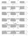
- FIG. 1 shows an example of the circuit diagram of the power semiconductor module apparatus which concerns on 1st Embodiment. It is a sectional side view which shows the structure of the power semiconductor module apparatus which concerns on 1st Embodiment. It is a 1st figure which shows the manufacturing method of the power semiconductor module apparatus which concerns on 1st Embodiment. It is a 2nd figure which shows the manufacturing method of the power semiconductor module apparatus which concerns on 1st Embodiment. It is a 3rd figure which shows the manufacturing method of the power semiconductor module apparatus which concerns on 1st Embodiment. It is a figure which shows the other structure of the power semiconductor module apparatus which concerns on 1st Embodiment.
- the semiconductor elements are fixed to each other on the first surface side (hereinafter referred to as the front surface side) while fixing a plurality of semiconductor elements arranged on the same plane with an insulating support.
- a first thick film plating layer as a first surface side electrode (hereinafter referred to as a front surface side electrode) electrically connected at the second surface side (hereinafter referred to as a back surface side) is electrically connected to the first thick film plating layer.
- a second thick film plating layer is formed as a two-sided electrode (hereinafter referred to as a back side electrode), and the first thick film plating layer and the second thick film plating layer are used as a support for supporting the semiconductor element from above and below. To form.
- the first semiconductor element is the high-side switching element SW1
- the second semiconductor element is the diode D1 corresponding to the switching element SW1
- the third semiconductor element is the low-side.
- a switching power supply circuit in which the switching element SW2 on the side and the fourth semiconductor element as the diode D2 corresponding to the switching element SW2 are described.
- the technology according to the present embodiment can be applied to power semiconductors other than the switching power supply circuit.
- switching elements elements such as Si and SiC can be used, and a combination of SiCMOS and diode, IGBT and diode, or the like is possible.
- FIG. 1 is a diagram showing an example of a circuit diagram of a power semiconductor module device according to this embodiment.
- a switching power supply circuit 1 converts a direct current into an alternating current and supplies it to a load.
- the direct current supplied to the switching power supply circuit 1 is converted into an alternating current by complementary switching of the switching elements.
- the high-side switching element SW1 and the low-side switching element SW2 are connected in series, and electric power is supplied from the connection point T to a load M such as a motor.
- a diode D1 and a diode D2 are connected to the switching elements SW1 and SW2 in antiparallel with the switching elements SW1 and SW2 so that the switching elements SW1 and SW2 are not destroyed by the counter electromotive force.
- the power semiconductor module device can manufacture individual modules by forming a plurality of modules collectively at the substrate level and finally dividing each module into modules. Details of the manufacturing method will be described later.
- FIG. 2 is a diagram showing a configuration of the power semiconductor module device according to the present embodiment.
- 2A is a side sectional view
- FIG. 2B is a top projection view
- FIG. 2C is a bottom projection view.
- the switching power supply circuit 1 constituting the power semiconductor module device includes a switching element SW1, a diode D1, a switching element SW2, and a diode D2, each of which is arranged on the same plane, and between the semiconductor elements.
- the insulating support 11 that is filled and supports each semiconductor element from at least the side surface direction, the first surface side electrode 12 that electrically connects the surface side of the switching element SW1 and the diode D1, and the switching element SW2 and the diode D2
- the first thick film plating layer 14 formed as the second surface side electrode 13 that electrically connects the surface side of the first surface, and the first back surface that electrically connects the back surfaces of the first switching element SW1 and the first diode D1.
- Side electrode 15 and back of second switching element SW2 and second diode D2 The second thick film plating layer 17 formed as the second back surface side electrode 16 that electrically connects the sides and the first back surface side electrode 15 and the second front surface side electrode 13 are electrically connected via the plating layer.
- the semiconductor elements arranged on the plane in a plane are supported from the side surface by the insulating support 11 interposed between the semiconductor elements, and are arranged in the vertical direction.
- the structure is more firmly supported by the first thick film plating layer 14 and the second thick film plating layer 17.
- the first thick film plating layer 14 and the second thick film plating layer 17 have a thickness of at least 50 ⁇ m (more preferably 100 ⁇ m, still more preferably 200 ⁇ m), and are electrically connected between semiconductor elements and externally. It is possible to connect and firmly support and fix each semiconductor element. That is, the first thick film plating layer 14 and the second thick film plating layer 17 can function as a wiring metal substrate, and in this embodiment, the wiring metal substrate as a component is unnecessary.
- the thick film plating layer is thinner than 50 ⁇ m, the amount of warpage due to thermal stress due to the difference in thermal expansion from the semiconductor element
- the thickness is 50 ⁇ m or more, the shape can be maintained as a structural material.
- electrode portions first surface side electrode 12, second surface side electrode 13, second surface side electrode 13 and second surface side electrode 13 in the first thick film plating layer 14 and the second thick film plating layer 17 are provided.
- the projected area of the first back surface side electrode 15 and the second back surface side electrode 16 is as shown in FIG. FIG. 2C shows the side having no gate electrode, that is, the first back side electrode 15 and the second back side electrode 16, which is at least 30% of the projected area of each semiconductor element.
- the size is at least 50% or more of the projected area of each semiconductor element, and it is possible to firmly support each semiconductor element from above and below while flowing a large current.
- the thicknesses of the first thick film plating layer 14 and the second thick film plating layer 17 are both 50 ⁇ m (more preferably 100 ⁇ m, more preferably 200 ⁇ m) or more and substantially the same thickness.
- the projected areas of the first surface side electrode 12 and the second surface side electrode 13 in the first thick film plating layer 14, and the first back surface side electrode 15 and the second back surface side electrode 16 in the second thick film plating layer 17. That is, the projected areas of the first surface side electrode 12 and the second surface side electrode 13 shown in FIG. 2B and the first back side electrode 15 and the second surface shown in FIG. 2C). (Difference from the projected area of the back electrode 16) is within 50%.
- the first surface side electrode 12 and the second surface side electrode 13 of the first thick film plating layer 14 and the first back surface side electrode 15 and the second back surface side electrode 16 of the second thick film plating layer 17 are, for example, Copper, copper alloy, nickel, nickel alloy, silver, aluminum, zinc, palladium and the like are preferable. Further, corrosion or the like may be prevented by covering at least the outermost surface with nickel plating.
- a wiring structure having excellent conductivity and excellent corrosion resistance at high temperatures can be obtained.
- a metal such as Cr, Ni, Ti, Pd, etc., or an alloy thereof or a multilayer of these metals, which has excellent adhesion to both the insulating material and the semiconductor element electrode, is a seed layer.
- the hot dip plating metal may be relatively low melting point Zn, Al or an alloy thereof.
- the semiconductor element may be a compound semiconductor element such as GaN or SiC having excellent heat resistance.
- any one or more of the above semiconductor elements may be SiC or GaN semiconductors. By doing so, it is possible to enhance the heat dissipation effect.
- the semiconductor elements of the switching element SW1, the diode D1, the switching element SW2, and the diode D2 are arranged on the same plane on the substrate 21, and are composed of the switching element SW1 and the diode D1.
- the conductor 18 is disposed between the first pair and the second pair including the switching element SW2 and the diode D2.
- the semiconductor elements and the conductors 18 are molded with a resin 22 so as to be embedded. As shown in FIG.
- grooves 23 are formed in the molded resin 22 so that the electrode portions of the semiconductor elements and the surface of the conductor 18 are exposed.
- general exposure and etching treatment using a resist can be applied.
- a resist is applied on the resin 22, and after performing a selective exposure process, the resist is removed to form an opening in the resist.
- the opening is subjected to dry etching or chemical treatment to remove the resin 22 in the opening to form the groove 23, and then the resist is removed.
- a heat-resistant mask is disposed in a portion to be opened, and after molding a resin, the mask is removed together with the resin thereon to form a groove. 23 may be formed.
- a seed 31 for plating is formed on the surface in a state where the region S1 where no electrode is formed is masked with a mask 24.
- a resist can be used as the mask 24, and the resist can be left only on the region S1 by performing exposure and selective removal by the method described above.
- the seed 31 is formed, as shown in FIG. 4B, the first thick film as the first surface side electrode 12 and the second surface side electrode 13 is performed by performing the plating process while the region S1 is masked.
- a plating layer 14 is formed. After the first thick film plating layer 14 is formed, the resist used as the mask 24 is removed, and then the substrate is peeled off as shown in FIG.
- a heat-resistant double-sided adhesive sheet that can be peeled off by heating or ultraviolet rays may be used in advance for bonding the substrate and the element.
- the back surface side As for the back surface side, as shown in FIG. 5 (A), as in the case of FIG. 4 (A), in the state where the region S2 where the electrode is not formed is masked with the mask 25, the back surface is subjected to the plating process. A seed 41 is formed.
- a resist process is performed so that the plating does not enter the space below the area S2 while the area S2 is masked, and the plating process is performed.
- the second thick film plating layer 17 is formed as the first back surface side electrode 15 and the second back surface side electrode 16.
- the resist used as the mask 25 is removed.
- FIG. 5C the whole is molded with the resin 26, and then is diced in units of modules.
- the power semiconductor module according to this embodiment is manufactured.
- the insulator of the resin 22 may be formed by using, for example, a sol-gel method to form ceramics or apply P glass.
- a layer of the resin 26 may be formed on the uppermost layer by built-up, and a heat radiating substrate or a heat radiating fin may be formed by metal melting (die casting method).
- the first pair 63 including the switching element SW1 and the diode D1 at the position of the conductor 18, the switching element SW2, and the diode without the conductor 18 being disposed.
- the semiconductor elements (switching element SW1, diode D1, switching element SW2, and diode D2) divided into the first pair 63 and the second pair 64 are electrically connected to form a stacked structure. Also good.
- a plating technique as disclosed in International Publication No. 2015/053356 can be used.
- a plurality of semiconductor elements arranged in a plane on a plane are fixed with an insulator, and the semiconductor elements are electrically connected on the front side and the back side.
- the mechanical support structure of the semiconductor element can be formed by plating, and the semiconductor module can be made a simple structure.
- a ceramic or resin substrate (substrate 72) in which conductive (for example, Cu) conductive wiring metal plates 71 are formed on both the front surface side and the back surface side is prepared.
- Temporarily fix with the temporary fixing tape 73 for support (FIG. 7 (A)).
- a through hole 75 larger than the semiconductor element 74 is provided in the substrate 72 of FIG. 7A (FIG. 7B), and the semiconductor element 74 is disposed in the through hole (FIG. 7C).
- the space between the substrate 72 and the semiconductor element 74 is filled with an insulating resin or a ceramic particle paste by a dispenser, for example (FIG. 7D).
- the temporary fixing tape 73 is peeled off (FIG.
- the front side is masked with, for example, a metal mask or mask tape in accordance with the wiring pattern, a seed layer is formed, a thick film plating metal is deposited, and a wiring is formed with the first thick film plating layer 14 (FIG. 7 (F)).
- a thick film plating metal is deposited on the back surface side, and wiring is formed by the second thick film plating layer 17 (FIG. 7G).
- the resin substrate may be, for example, a polyimide material with conductive wiring metal plates bonded on both sides.
- the thickness is preferably about 50 ⁇ m to 1 mm for the insulating material and about 50 ⁇ m to 0.5 mm for the copper plate.
- the power semiconductor module device according to the present embodiment will be described with reference to FIGS.
- one of the electrodes on the front surface side or the back surface side is formed by the thick film plating described in each of the above embodiments, and the conductive wiring metal plate is used for the electrodes on the other surface side. Is formed.
- the electrode connection surfaces of the conductive wiring metal plate and the semiconductor element are plated and connected via the edge portion.
- the surface that requires patterning is formed with an electrode using a conductive wiring metal plate, and the surface that does not require patterning is formed by thick film plating.
- the description which overlaps with each said embodiment is abbreviate
- FIG. 8 is a first diagram showing the configuration of the power semiconductor module device according to the present embodiment.
- 8 and 9 show a structure in which a diode and a MOSFET are used as an example.
- 8A is a top view
- FIG. 8B is a cross-sectional view taken along arrow a in FIG. 8A.
- a semiconductor element 82 here, a diode 82a and a MOSFET 82b
- a ceramic substrate 81 on which conductive wiring metal plates are disposed on both sides, and a ceramic material is placed in the gap between the side surfaces of each semiconductor element 82. And is supported from the side surface direction of the semiconductor element 82.
- the lead 83a of the conductive wiring metal plate 83 and the electrode 82c of the semiconductor element 82 are connected by plating through the edge portion of the bump 84.
- the plating solution can sufficiently flow between the electrode 82c of the semiconductor element 82 and the connection surface of the lead 83a.
- the back surface side has a structure in which the thick film plating layer 85 is formed as a wiring.
- FIG. 9A is a top view
- FIG. 9B is a cross-sectional view taken along arrow a in FIG. 9A.
- conductive wiring metal plates are provided on both sides.
- a semiconductor element 82 is embedded in the disposed ceramic substrate 81, and a gap between the side surfaces of the semiconductor element 82 is filled with a ceramic material and supported from the side surface direction of the semiconductor element 82.
- the connection surface of the lead 83a of the conductive wiring metal plate 83 is formed in a mountain shape, and is connected to the electrode 82c of the semiconductor element 82 by plating through the edge portion of the mountain shape.
- the back surface side has a structure in which the thick film plating layer 85 is formed as a wiring.
- FIG. 10 is a diagram showing a manufacturing process of the power semiconductor module device according to the present embodiment.
- a ceramic or resin substrate substrate 92
- a through hole 95 larger than the semiconductor element 82 here, the diode 82a and the MOSFET 82b
- a conductive wiring metal plate 83 is bonded to the front surface side and back surface side of the substrate 92 (FIG. 10B).
- the conductive wiring metal plate 83 on the surface side is at least bonded to a region other than the through hole 95, and a plurality of leads 83a are arranged in the region of the through hole 95 at intervals. These leads 83a are bonded so that the position of the surface electrode of the semiconductor element 82 embedded in the through-hole 95 in the process described later corresponds to the position of the angled edge portion 83b formed in the lead 83a. . Further, the conductive wiring metal plate 83 on the back surface side is bonded to a region other than the through hole 95, and the region of the through hole 95 is opened.
- the semiconductor element 82 is fitted into the through-hole 95 from the opening on the back side, and the space between the substrate 92 and the semiconductor element 82 is filled and fixed with an insulating resin or ceramic particles by a dispenser, for example (FIG. 10C).
- the edge portion 83b of the lead 83a is plated to connect the surface side conductive wiring metal plate 83 and the semiconductor element 82 (FIG. 10D).
- a copper thin film 98 is deposited on the back side electrode of the semiconductor element 82 by sputtering (FIG. 10E), and then a thick plating layer 85 having a necessary thickness is formed in consideration of the standard current amount. A layer is formed (FIG. 10F).
- the mountain-shaped protrusions formed on the connection surface of the lead 83a of the conductive wiring metal plate 83 are preferably formed at an inclination angle of about 5 to 30 degrees with respect to the contact surface.
- the shape of the protrusion may be a shape that forms an edge portion such as a trapezoidal shape, a circular arc shape, a wave shape, etc. in addition to the mountain shape.
- FIGS. 11 and 12 not only the front side but also the back side can be connected to the conductive wiring metal plate via the edge portion to form a current wiring layer.
- FIGS. 11A and 12A are top views
- FIGS. 11B and 12B are bottom views
- FIGS. 11C and 12C are FIGS.
- FIG. 12 is a cross-sectional view taken along arrow a in FIG.
- a heat spreader is formed by plating on the surface of the conductive wiring metal plate 83 of the power semiconductor module device according to the third embodiment.
- a heat spreader In the power semiconductor module device, it is necessary not only to connect the semiconductor element and the conductive wiring metal plate 83 but also to connect a metal (heat spreader) having high thermal conductivity for heat dissipation.
- a metal heat spreader
- the solder since the solder has poor thermal conductivity, if the solder is interposed between the heat spreader and the conductive wiring metal plate 83, the heat spreader is used. The effect of can not be fully demonstrated. Therefore, in this embodiment, a heat spreader is directly formed on the surface of the conductive wiring metal plate 83 by plating without using a material having poor thermal conductivity such as solder.
- the plating in this embodiment includes electrolytic plating, electroless plating, and hot dipping.
- electroplating and electroless plating a plated metal is directly deposited on the surface of the conductive wiring metal plate 83 to form a heat spreader. You may make it do.
- hot dipping zinc or aluminum having a relatively low melting point may be melted and cast, or a molten metal may be sprayed from a nozzle as in a three-dimensional printer to form a heat spreader.
- FIG. 13 is a diagram illustrating an example of a heat spreader forming method in the power semiconductor module device according to the present embodiment.
- the heat spreader forming method shown in FIG. 13 is directed to the surface of the conductive wiring metal plate 83 when the conductive wiring metal plate 83 is provided on the front surface side and the back surface side is formed of the thick film plating layer 85 as shown in FIG.
- the process in the case where the heat spreader is formed with a build-up type after the power semiconductor module device shown in FIG. 9 is molded with resin is shown. Thick copper plating is applied on the back side, and if the heat spreader is not formed on the back side, either do not cover it with mold resin, or remove the resin by polishing after molding. May be.
- the power semiconductor module device 1 molded with the resin 122 is prepared (FIG. 13A), a hole in the conductive wiring metal plate 83 is drilled with a laser, and a lift-off resist 121 is formed in a place where the heat spreader 120 is not required. Apply. At this time, the resin on the back surface side is removed by polishing (FIG. 13B). A Ti—Au seed 31 is formed on the surface side of the power semiconductor module device 1 formed in FIG. 13B for plating (FIG. 13C). The resist 121 is removed, and at the same time, the seed layer at the resist portion is removed. A heat spreader 120 is formed by plating (FIG. 13D).
- the plating treatment at this time may use any method of electrolytic plating, electroless plating, and hot dipping as described above. Since the seed 31 is a metal of about 1 ⁇ m or less, even if it has a lower thermal conductivity than the material of the heat spreader, it hardly causes a reduction in heat dissipation.
- the heat spreader 120 for diffusing heat is formed on the surface of the conductive wiring metal plate 83 by plating, so that heat can be efficiently released.
- the heat spreader 120 is formed by plating, the heat of the conductive wiring metal plate 83 is efficiently transferred to the heat spreader 120 without interposing a solder having poor heat conductivity between the conductive wiring metal plate 83 and the heat spreader 120. It becomes possible to communicate well.
- each back surface side has the same structure as the front surface side in FIG. 13, and the process shown in FIG.
- the heat spreader is formed on both sides of the module device. Note that a heat spreader may not be formed on an electrode portion that does not require heat dissipation, such as a gate electrode.
Landscapes
- Cooling Or The Like Of Semiconductors Or Solid State Devices (AREA)
- Engineering & Computer Science (AREA)
- Manufacturing & Machinery (AREA)
- Dicing (AREA)
Abstract
平面上に配列された半導体素子間を絶縁体で支持すると共に、表面側又は裏面側の少なくとも一方から厚膜めっきにより半導体素子間を電気的に接続しつつ、上方向又は下方向の少なくとも一方から支持するパワー半導体モジュール装置及びパワー半導体モジュール製造方法を提供する。 平面上に面一に配列する複数の半導体素子間が絶縁性の支持体で固定され、当該半導体素子同士を表面側又は裏面側の少なくとも一方の面で電気的に接続する第1面側電極として形成されている第1厚膜めっき層14を有しており、第1厚膜めっき層14が半導体素子を上下方向の少なくとも一方から支持する。また、前記第1面側電極と反対側の面に、前記半導体素子の電極とエッジを介して接続する接続面を有する配線金属基板83を有することが可能であり、前記第1厚膜めっき層14と前記配線金属板83とが半導体素子を上下方向から支持することができる。
Description
本発明は、絶縁材料を介して配列される半導体素子の表面側又は裏面側の少なくとも一方を厚膜めっきで配線形成するパワー半導体モジュール装置等に関する。
従来、半導体素子電極と外部端子とを接続するのにワイヤボンディングや半田接続が利用されていた。しかしながら、ワイヤボンディングでは配線長が長くなると共に、超音波接合により半導体素子への応力負荷によるダメージが懸念される。また、半田接続の場合は、半導体素子の高温時における動作の信頼性の確保が困難になってしまう。
そこで、めっき接続により半導体素子電極と外部端子とを接続することが有効と考えられるが、めっき接続の場合には、接続部分にボイドが発生してしまい、品質が低下してしまう可能性がある。そこで、めっき接続においてボイドの発生を防止する技術として、例えば特許文献1、2に示す技術が開示されている。
特許文献1に示す技術は、半導体素子1と金属板2との間において、突起3を中心に放射状にメッキ4が成長する構成としたものである。特許文献2に示す技術は、電気的に接続される電気回路の複数の電極間の少なくとも一部を直接又は間接的に接触させ、当該接触部分の周辺にメッキ液が流通した状態で電極間をメッキして接続するものである。
また、半導体素子などをモールド樹脂で埋め込んで再構成する技術としてファンアウトウエハレベルパッケージ(FOWLP)技術が知られている(例えば、特許文献3を参照)。
特許文献1、2に示す技術は、いずれもめっき接続においてボイドの発生を抑制できるものであるが、個々の半導体素子を配列し、それぞれの電極をめっきで接合する技術ではない。また、FOWLPについては、多層構造で外部端子と接続するものであり、平面上に配列された個々の部品間を厚膜単層で接続し、半導体を支持するものではない。
本発明は、平面上に配列された半導体素子間を絶縁体で支持すると共に、表面側又は裏面側の少なくとも一方から厚膜めっきにより半導体素子間を電気的に接続しつつ、上方向又は下方向の少なくとも一方から支持するパワー半導体モジュール装置及びパワー半導体モジュール製造方法を提供する。
本発明に係るパワー半導体モジュール装置は、平面上に面一に配列する複数の半導体素子間が絶縁性の支持体で固定され、前記半導体素子同士を表面側又は裏面側の少なくとも一方の面で電気的に接続する第1面側電極として形成されている第1厚膜めっき層を有しており、前記第1厚膜めっき層が前記半導体素子を上下方向の少なくとも一方から支持するものである。
このように、本発明に係るパワー半導体モジュール装置においては、平面上に面一に配列する複数の半導体素子間が絶縁性の支持体で固定され、前記半導体素子同士を表面側又は裏面側の少なくとも一方の面で電気的に接続する第1面側電極として形成されている第1厚膜めっき層を有しており、前記第1厚膜めっき層が前記半導体素子を上下方向の少なくとも一方から支持するため、半導体素子の機械的な支持構造をめっきで形成することが可能となり、半導体モジュールをシンプルな構造にすることができるという効果を奏する。
本発明に係るパワー半導体モジュール装置は、前記第1面側電極と反対側の面に、前記半導体素子の電極とエッジを介してめっき接続する接続面を有する導電配線金属板を有しており、前記第1厚膜めっき層と前記導電配線金属板とが前記半導体素子を上下方向から支持するものである。
このように、本発明に係るパワー半導体モジュール装置においては、前記第1面側電極と反対側の面に、前記半導体素子の電極とエッジを介して接続する接続面を有する導電配線金属板を有しており、前記第1厚膜めっき層と前記導電配線金属板とが前記半導体素子を上下方向から支持するため、一方の面にのみパターニングが必要な場合などに、導電配線金属板により簡単なプロセスで配線することが可能になると共に、半導体素子の電極と導電配線金属板の接続面とがエッジを介することで、半導体素子電極とリードの接続面との間にめっき液を十分に流通させることができ、ボイド等を発生させることなく高品質なめっき接続を実現することができる。
なお、上記エッジとは、電極面とめっき接続する被接合体との界面が山形、円錐、ボール、円筒状の形状で形成され、線状もしくは点状、又は球状もしくは円状の頂点の突起部を指し、電極面とエッジ部周辺の間隙部をエッジを介しためっき接続をすることで、強固で、熱、電流損失が少ない伝達接合部を形成することができる。
本発明に係るパワー半導体モジュール装置は、前記第1面側電極と反対側の面に、前記半導体素子同士を電気的に接続する第2面側電極として形成されている第2厚膜めっき層を有しており、前記第1厚膜めっき層と前記第2厚膜めっき層とが前記半導体素子を上下方向から支持するものである。
このように、本発明に係るパワー半導体モジュール装置においては、前記第1面側電極と反対側の面に、前記半導体素子同士を電気的に接続する第2面側電極として形成されている第2厚膜めっき層とを有しており、前記第1厚膜めっき層と前記第2厚膜めっき層とが前記半導体素子を上下方向から支持するため、半導体素子の機械的な支持構造をめっきで形成することが可能となり、半導体モジュールをシンプルな構造にすることができるという効果を奏する。また、第1面側電極と第2面側電極とを同一のめっきプロセスで簡単に形成することが可能になるという効果を奏する。
本発明に係るパワー半導体モジュール装置は、前記第1厚膜めっき層と前記第2厚膜めっき層とが略同一の厚さで、前記第1厚膜めっき層の表面側電極の投影面積が、前記半導体素子の投影面積の30%以上であり、前記第2厚膜めっき層の裏面側電極の投影面積が、前記半導体素子の投影面積の50%以上であり、前記表面側電極の投影面積と前記裏面側電極の投影面積との差が50%以内とするものである。
このように、本発明に係るパワー半導体モジュール装置においては、前記第1厚膜めっき層と前記第2厚膜めっき層とが略同一の厚さで、前記第1厚膜めっき層の表面側電極の投影面積が、前記半導体素子の投影面積の30%以上であり、前記第2厚膜めっき層の裏面側電極の投影面積が、前記半導体素子の投影面積の50%以上であり、前記表面側電極の投影面積と前記裏面側電極の投影面積との差が50%以内であるため、表面側及び裏面側の電極で放熱効果を高めることができると共に、表面側と裏面側との熱膨張による影響の差を最小限に抑えて高品質に保つことができるという効果を奏する。
本発明に係るパワー半導体モジュール装置は、前記第1厚膜めっき層及び前記第2厚膜めっき層のめっきの厚さが少なくとも50μm以上とするものである。
このように、本発明に係るパワー半導体モジュール装置においては、前記第1厚膜めっき層及び前記第2厚膜めっき層のめっきの厚さが少なくとも50μm以上であるため、パワー半導体モジュールで大電流を通電しつつ、半導体素子を強固に支持することができるという効果を奏する。また、厚膜配線が形成された後に150℃以上の温度で熱処理することが望ましく、その場合に、50μmより薄いと半導体素子との熱膨張差による熱応力で反り量が増大してしまうが、50μm以上の厚みとすることで、構造材として形状を維持することができるという効果を奏する。なお、めっきの厚みは、より好ましくは100μm以上、さらに好ましくは200μm以上であってもよい。
本発明に係るパワー半導体モジュール装置は、前記第1厚膜めっき層及び/又は前記第2厚膜めっき層の表面の一部又は全部が1μm以上の厚さのNi又はNi合金で被覆されているものである。
このように、本発明に係るパワー半導体モジュール装置においては、前記第1厚膜めっき層及び/又は前記第2厚膜めっき層の表面の一部又は全部が1μm以上の厚さのNi又はNi合金で被覆されているため、導電性に優れ、高温での耐食性にも優れた配線構造とすることができるという効果を奏する。
本発明に係るパワー半導体モジュール装置は、複数の前記半導体素子のうち一の前記半導体素子がスイッチング素子であり、当該スイッチング素子以外の他の前記半導体素子のうち少なくとも一の前記半導体素子がダイオードであり、前記半導体素子間に、前記第1面側電極と前記第2面側電極とを電気的に接続するための前記半導体素子と略同一の厚みを有する導電体が配設されており、当該導電体が前記第1面側電極及び前記第2面側電極と電気的に接続されているものである。
このように、本発明に係るパワー半導体モジュール装置においては、複数の前記半導体素子のうち一の前記半導体素子がスイッチング素子であり、当該スイッチング素子以外の他の前記半導体素子のうち少なくとも一の前記半導体素子がダイオードであり、前記半導体素子間に、前記第1面側電極と前記第2面側電極とを電気的に接続するための前記半導体素子と略同一の厚みを有する導電体が配設されており、当該導電体が前記第1面側電極及び前記第2面側電極と電気的に接続されているため、上記に示したようなシンプルな構造で高性能なスイッチング素子を実現することができると共に、第1面側電極と第2面側電極とを導電体を介しためっき接続により電気的に確実に接続することができるという効果を奏する。
本発明に係るパワー半導体モジュール装置は、前記導電配線金属板の表面に熱を拡散するためのヒートスプレッダがめっきで形成されているものである。
このように、本発明に係るパワー半導体モジュール装置においては、導電配線金属板の表面に熱を拡散するためのヒートスプレッダがめっきで形成されているため、熱を効率よく放出することができるという効果を奏する。また、ヒートスプレッダがめっきで形成されているため、導電配線金属板とヒートスプレッダとの間に半田等を介することなく、導電配線金属板の熱をヒートスプレッダに効率よく伝達することが可能になるという効果を奏する。
以下、本発明の実施の形態を説明する。また、本実施形態の全体を通して同じ要素には同じ符号を付けている。
(本発明の第1の実施形態)
本実施形態に係るパワー半導体モジュール装置について、図1ないし図7を用いて説明する。本実施形態に係るパワー半導体モジュール装置は、平面上に面一に配列する複数の半導体素子間を絶縁性の支持体で固定しつつ、半導体素子同士を第1面側(以下、表面側という)で電気的に接続する第1面側電極(以下、表面側電極という)として第1厚膜めっき層と、半導体素子同士を第2面側(以下、裏面側という)で電気的に接続する第2面側電極(以下、裏面側電極という)として第2厚膜めっき層とを形成し、第1厚膜めっき層と第2厚膜めっき層とを半導体素子を上下方向から支持する支持体として形成するものである。
本実施形態に係るパワー半導体モジュール装置について、図1ないし図7を用いて説明する。本実施形態に係るパワー半導体モジュール装置は、平面上に面一に配列する複数の半導体素子間を絶縁性の支持体で固定しつつ、半導体素子同士を第1面側(以下、表面側という)で電気的に接続する第1面側電極(以下、表面側電極という)として第1厚膜めっき層と、半導体素子同士を第2面側(以下、裏面側という)で電気的に接続する第2面側電極(以下、裏面側電極という)として第2厚膜めっき層とを形成し、第1厚膜めっき層と第2厚膜めっき層とを半導体素子を上下方向から支持する支持体として形成するものである。
本実施形態に係るパワー半導体モジュール装置おいては、例えば第1の半導体素子をハイサイド側のスイッチング素子SW1、第2の半導体素子をスイッチング素子SW1に対応するダイオードD1、第3の半導体素子をローサイド側のスイッチング素子SW2、第4の半導体素子をスイッチング素子SW2に対応するダイオードD2とするスイッチング電源回路について説明する。なお、スイッチング電源回路以外のパワー半導体についても、本実施形態に係る技術を適用可能である。また、スイッチング素子としては、Si、SiC等の素子を利用することが可能であり、SiCMOSとダイオード、IGBTとダイオードなどの組み合わせが可能である。
図1は、本実施形態に係るパワー半導体モジュール装置の回路図の一例を示す図である。図1において、スイッチング電源回路1は、直流電流を交流電流に変換して負荷に供給するものである。スイッチング電源回路1に供給された直流電流はスイッチング素子の相補的な切り替えにより交流電流に変換される。ハイサイド側のスイッチング素子SW1とローサイド側のスイッチング素子SW2とは、直列接続されており、その接続点Tから例えばモータなどの負荷Mに対して電力が供給される。スイッチング素子SW1,SW2には、逆起電力により当該スイッチング素子SW1,SW2が破壊されないように、それぞれのスイッチング素子SW1,SW2と逆並列にダイオードD1及びダイオードD2が接続されている。
なお、本実施形態に係るパワー半導体モジュール装置は、基板レベルで一括して複数のモジュールを形成し、最後に各モジュール単位に分割することで、個々のモジュールを製造することができる。製造方法の詳細については後述する。
図2は、本実施形態に係るパワー半導体モジュール装置の構成を示す図である。図2(A)が側断面図、図2(B)が上面投影図、図2(C)が下面投影図である。パワー半導体モジュール装置を構成するスイッチング電源回路1は、それぞれが平面上に面一に配列されているスイッチング素子SW1、ダイオードD1、スイッチング素子SW2及びダイオードD2の各半導体素子と、当該各半導体素子間に充填されて当該各半導体素子を少なくとも側面方向から支持する絶縁支持体11と、スイッチング素子SW1及びダイオードD1の表面側を電気的に接続する第1表面側電極12、並びに、スイッチング素子SW2及びダイオードD2の表面側を電気的に接続する第2表面側電極13として形成される第1厚膜めっき層14と、第1スイッチング素子SW1及び第1ダイオードD1の裏面側を電気的に接続する第1裏面側電極15、並びに、第2スイッチング素子SW2及び第2ダイオードD2の裏面側を電気的に接続する第2裏面側電極16として形成される第2厚膜めっき層17と、第1裏面側電極15と第2表面側電極13との間をめっき層を介して電気的に接続するための導電体18とを備える。
図2(A)に示すように、平面上に面一に配列された各半導体素子は、その半導体素子間に介在している絶縁支持体11により側面方向から支持されると共に、上下方向から第1厚膜めっき層14及び第2厚膜めっき層17でより強固に支持される構造となっている。第1厚膜めっき層14及び第2厚膜めっき層17は、少なくとも50μm(より好ましくは100μm、さらに好ましくは200μm)以上の厚さを有しており、半導体素子間及び外部との電気的な接続を行うと共に、各半導体素子を強固に支持固定することが可能となる。すなわち、第1厚膜めっき層14及び第2厚膜めっき層17は配線金属基板として機能することが可能となり、本実施形態においては、部品としての配線金属基板が不要な構造となっている。また、厚膜めっき層が形成された後に150℃以上の温度で熱処理することが望ましいため、その場合に、厚膜めっき層が50μmより薄いと半導体素子との熱膨張差による熱応力で反り量が増大してしまうが、50μm以上の厚みとすることで、構造材として形状を維持することが可能となる。
また、図2(B)、(C)に示すように、第1厚膜めっき層14及び第2厚膜めっき層17における電極部分(第1表面側電極12、第2表面側電極13、第1裏面側電極15及び第2裏面側電極16)の投影面積が、ゲート電極を有する側、すなわち第1表面側電極12及び第2表面側電極13については、図2(B)に示すように、各半導体素子の投影面積の少なくとも30%以上の大きさとなっており、ゲート電極を有しない側、すなわち第1裏面側電極15及び第2裏面側電極16については、図2(C)に示すように、各半導体素子の投影面積の少なくとも50%以上の大きさとなっており、いずれも大電流を流しつつ、各半導体素子を上下方向から強固に支持することが可能となっている。
また、上述したように、第1厚膜めっき層14及び第2厚膜めっき層17の厚さがどちらも50μm(より好ましくは100μm、さらに好ましくは200μm)以上で略同一の厚さを有しており、第1厚膜めっき層14における第1表面側電極12及び第2表面側電極13の投影面積と、第2厚膜めっき層17における第1裏面側電極15及び第2裏面側電極16の投影面積との差(すなわち、図2(B)に示す第1表面側電極12及び第2表面側電極13の投影面積と、図2(C)に示す第1裏面側電極15及び第2裏面側電極16の投影面積との差)が50%と以内となっている。つまり、第1厚膜めっき層14と第2厚膜めっき層17とにおいて熱膨張の差が発生しにくいため、熱膨張による変形応力等によって品質が低下するのを防止することが可能となる。特に、多層に積層された際には上下間の撓みを最小限に抑えて品質を保つことが可能となる。
なお、第1厚膜めっき層14の第1表面側電極12及び第2表面側電極13、並びに、第2厚膜めっき層17の第1裏面側電極15及び第2裏面側電極16は、例えば、銅、銅合金、ニッケル、ニッケル合金、銀、アルミニウム、亜鉛、パラジウム等であることが好ましい。また、少なくとも最表面がニッケルめっきで被覆されることで腐食等が防止されるようにしてもよい。
例えば、Cuめっきにより主めっき層を形成し、表面に1μm以上の厚みで被覆層を形成することで、導電性に優れ、高温での耐食性にも優れた、配線構造とすることができる。めっきするための下地層には、絶縁材料及び半導体素子電極ともに密着性の優れるCr、Ni、Ti、Pdなどの金属、又は、それらの合金もしくはそれらの金属の複層をスパッタ蒸着し、シード層として金属めっきをすることができる。
また、電極側からCr、Ni、Pd又は最表面には、さらにめっき金属と同種のもの又は酸化防止のためのAgもしくはAu膜を形成することが好ましい。
さらに、第1厚膜めっき層14及び第2厚膜めっき層17を形成するためのめっき処理の方法としては、電気めっきの他溶融めっきを利用することが可能である。溶融めっき金属としては、比較的低融点のZn、Al又はそれらの合金としてもよい。その場合の半導体素子は、耐熱性に優れるGaNやSiCなどの化合物半導体素子としてもよい。
さらにまた、上記各半導体素子のいずれか1つ又は複数が、SiC又はGaN半導体であってもよい。そうすることで、放熱効果を高めることが可能となる。
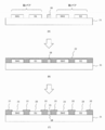
次に、本実施形態に係るパワー半導体モジュール装置の製造方法について説明する。まず、図3(A)に示すように、基板21上にスイッチング素子SW1、ダイオードD1、スイッチング素子SW2及びダイオードD2の各半導体素子が面一に配列されると共に、スイッチング素子SW1及びダイオードD1からなる第1ペアと、スイッチング素子SW2及びダイオードD2からなる第2ペアとの間に導電体18が配置される。各半導体素子及び導電体18が配置されると、図3(B)に示すように、上記の各半導体素子と導電体18を埋め込むように樹脂22でモールドされる。モールドされた樹脂22に対して、図3(C)に示すように、上記各半導体素子の電極部分及び導電体18の表面が露出されるように溝23を形成する。この処理にはレジストを用いた一般的な露光、エッチング処理が適用できる。例えば、樹脂22の上にレジストを塗布し、選択的な露光処理を行ったあとレジスト除去を行い、レジストに開口部を形成する。開口部をドライエッチング又は薬液処理を行って、開口部の樹脂22を除去することで溝23を形成し、その後、レジストを除去する。なお、他の方法として、図3(A)のプロセスの次に、開口すべき部分に耐熱性のマスクを配置しておき、樹脂をモールドした後、マスクをその上の樹脂ごと除去して溝23を形成してもよい。
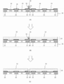
続いて、図4(A)に示すように、電極を形成しない領域S1をマスク24でマスクした状態で、表面にめっき処理のためのシード31を形成する。マスク24としてレジストを用いることができ、先に説明したような方法で露光と選択的除去を行うことで領域S1上のみにレジストを残すことができる。シード31が形成されると、図4(B)に示すように、領域S1をマスクした状態のままめっき処理を行って第1表面側電極12及び第2表面側電極13としての第1厚膜めっき層14が形成される。第1厚膜めっき層14を形成したあとマスク24として用いたレジストを除去し、続いて図4(C)に示すように、基板を剥離し、裏面側の工程へと進む。なお、基板剥離を容易にするため、予め基板と素子の接着に加熱や紫外線で剥離可能な耐熱性両面接着シートを用いるようにしてもよい。
裏面側については、図5(A)に示すように、図4(A)の場合と同様に、電極を形成しない領域S2をマスク25でマスクした状態で、裏面側表面にめっき処理のためのシード41を形成する。裏面側のシード41が形成されると、図5(B)に示すように、領域S2をマスクした状態のまま領域S2の下方空間にめっきが侵入しないようにレジスト処理を施し、めっき処理を行って第1裏面側電極15及び第2裏面側電極16としての第2厚膜めっき層17が形成される。第2厚膜めっき層17を形成したあとマスク25として用いたレジストを除去し、続いて図5(C)に示すように、全体を樹脂26でモールドした後、モジュール単位でダイシングすることで、本実施形態に係るパワー半導体モジュールが製造される。
なお、上記めっき処理は、電解めっき、無電解めっき又は溶融めっきのいずれかを適用することが可能である。また、樹脂22の絶縁体は、例えばゾルゲル法を用いて行うようにして、セラミックスを形成するか、Pガラスを塗布してもよい。さらに、図5(C)に示すように、最上層にビルトアップで樹脂26の層が形成され、さらに放熱基板又は放熱フィンを金属溶融(ダイキャスト法)により形成するようにしてもよい。
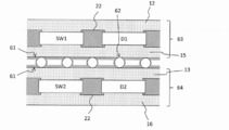
また、上記の製造工程において、図6に示すように、導電体18を配設せずに、導電体18の位置でスイッチング素子SW1及びダイオードD1からなる第1ペア63と、スイッチング素子SW2及びダイオードD2からなる第2ペア64とに分断するようにダイシングし、それぞれの部品を外部で接続するか縦に積層し、近接する面61においてワイヤやボール等のエッジ部62を介してめっき接続することで、第1ペア63と第2ペア64とに分断されたそれぞれの半導体素子(スイッチング素子SW1、ダイオードD1、スイッチング素子SW2及びダイオードD2)を電気的に接続して積層構造を形成するようにしてもよい。このとき、例えば、国際公開第2015/053356号に開示されているようなめっき技術を用いることができる。
以上のように、本実施形態に係るパワー半導体モジュール装置においては、平面上に面一に配列する複数の半導体素子間を絶縁体で固定し、半導体素子同士を表面側及び裏面側で電気的に接続し、それぞれに第1厚膜めっき層及び第2厚膜めっき層とを有しており、第1厚膜めっき層と第2厚膜めっき層とが半導体素子を上下方向から支持するため、半導体素子の機械的な支持構造をめっきで形成することが可能となり、半導体モジュールをシンプルな構造にすることができる。
(本発明の第2の実施形態)
本実施形態に係るパワー半導体モジュール装置の製造方法について、図7を用いて説明する。前記第1の実施形態における図3~図5に示したパワー半導体モジュール装置の製造方法以外にも、図7に示すような製造方法を用いてパワー半導体モジュールを製造することができる。なお、本実施形態において、前記第1の実施形態と重複する説明は省略する。
本実施形態に係るパワー半導体モジュール装置の製造方法について、図7を用いて説明する。前記第1の実施形態における図3~図5に示したパワー半導体モジュール装置の製造方法以外にも、図7に示すような製造方法を用いてパワー半導体モジュールを製造することができる。なお、本実施形態において、前記第1の実施形態と重複する説明は省略する。
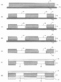
具体的には、表面側及び裏面側の両面に導電性(例えば、Cu等)の導電配線金属板71が形成されているセラミックス又は樹脂基板(基板72)を用意し、表面側となる面を支持用の仮止めテープ73で仮止めする(図7(A))。図7(A)の基板72に半導体素子74よりも大きい貫通孔75を設け(図7(B))、貫通孔内に半導体素子74を配置する(図7(C))。基板72と半導体素子74間を、例えばディスペンサにより絶縁樹脂又はセラミックス粒子ペースト等で充填する(図7(D))。充填された絶縁樹脂又はセラミックス粒子ペーストが硬化したら、仮止めテープ73を剥がす(図7(E))。表面側に対して、配線パターンに合わせて、例えばメタルマスクやマスクテープでマスクし、シード層を形成し、厚膜めっき金属を堆積させて第1厚膜めっき層14で配線を形成する(図7(F))。裏面側も同様に厚膜めっき金属を堆積させて第2厚膜めっき層17で配線を形成する(図7(G))。このような製造方法を用いることで、図2に示す構造と同様の構造を形成することが可能となる。
なお、樹脂基板は、例えばポリイミド材で両面に導電配線金属板を接着したものでもよい。また、厚みは絶縁材が50μmから1mm、銅板は50μm~0.5mm程度が好適である。
(本発明の第3の実施形態)
本実施形態に係るパワー半導体モジュール装置について、図8ないし図11を用いて説明する。本実施形態に係るパワー半導体モジュール装置は、表面側又は裏面側のいずれか一方の電極を前記各実施形態において説明した厚膜めっきで形成し、他の面側の電極については、導電配線金属板で形成するものである。このとき、導電配線金属板と半導体素子との電極接続面はエッジ部を介してめっき接続されるものである。本実施形態においては、例えば、パターニングが必要な方の面を導電配線金属板で電極形成し、パターニングが不要な面を厚膜めっきで電極形成する。なお、本実施形態において前記各実施形態と重複する説明は省略する。
本実施形態に係るパワー半導体モジュール装置について、図8ないし図11を用いて説明する。本実施形態に係るパワー半導体モジュール装置は、表面側又は裏面側のいずれか一方の電極を前記各実施形態において説明した厚膜めっきで形成し、他の面側の電極については、導電配線金属板で形成するものである。このとき、導電配線金属板と半導体素子との電極接続面はエッジ部を介してめっき接続されるものである。本実施形態においては、例えば、パターニングが必要な方の面を導電配線金属板で電極形成し、パターニングが不要な面を厚膜めっきで電極形成する。なお、本実施形態において前記各実施形態と重複する説明は省略する。
図8は、本実施形態に係るパワー半導体モジュール装置の構成を示す第1の図である。なお、図8及び図9においては、一例としてダイオードとMOSFETを用いた場合の構造を示している。図8(A)は上面図、図8(B)は図8(A)における矢印aの断面図である。図8において、両面に導電配線金属板が配設されたセラミックス基板81に半導体素子82(ここでは、ダイオード82aとMOSFET82b)が埋め込まれており、それぞれの半導体素子82の側面の隙間にはセラミックス材料が充填されて、半導体素子82の側面方向から支持している。表面側は、導電配線金属板83のリード83aと半導体素子82の電極82cとがバンプ84のエッジ部分を介してめっきにより接続されている。図8(B)に示すように、リード83a間には隙間が空いていることから、半導体素子82の電極82cとリード83aの接続面との間にめっき液を十分に流通することができるため、エッジ部分を介しためっき接続を行うことで、ボイド等を発生させることなく高品質なめっき接続を実現することができる。裏面側は、上記第1の実施形態において説明したように、厚膜めっき層85を配線として形成する構造となっている。
図9において、図9(A)は上面図、図9(B)は図9(A)における矢印aの断面図を示しており、図8の場合と同様に、両面に導電配線金属板が配設されたセラミックス基板81に半導体素子82が埋め込まれており、半導体素子82の側面の隙間にはセラミックス材料が充填されて、半導体素子82の側面方向から支持している。表面側は、導電配線金属板83のリード83aの接続面が山形に形成されており、その山形のエッジ部分を介して半導体素子82の電極82cとめっきにより接続されている。ここでも、図9(A)に示すように、リード83a間には隙間が空いていることから、半導体素子82の電極82cとリード83aの接続面との間にめっき液を十分に流通することができるため、エッジ部分を介しためっき接続を行うことで、ボイド等を発生させることなく高品質なめっき接続を実現することができる。裏面側は、上記第1の実施形態において説明したように、厚膜めっき層85を配線として形成する構造となっている。
次に、本実施形態に係るパワー半導体モジュール装置の製造方法について説明する。ここでは、図9の構造について説明する。図10は、本実施形態に係るパワー半導体モジュール装置の製造工程を示す図である。まず、セラミックス又は樹脂基板(基板92)を用意し、半導体素子82(ここでは、ダイオード82aとMOSFET82b)よりも大きい貫通孔95を設ける(図10(A))。基板92の表面側及び裏面側に導電配線金属板83を接着する(図10(B))。このとき、表面側の導電配線金属板83は、貫通孔95以外の領域に少なくとも接着され、貫通孔95の領域については、間隔を空けて複数のリード83aが配設されている。これらのリード83aは、後述する工程で貫通孔95内に埋め込まれる半導体素子82の表面電極の位置と、リード83aに形成されている山形のエッジ部分83bの位置とが対応するように接着される。また、裏面側の導電配線金属板83は、貫通孔95以外の領域に接着され、貫通孔95の領域は開口した状態となる。
裏面側の開口部から半導体素子82を貫通孔95に嵌め込み、基板92と半導体素子82間を、例えばディスペンサにより絶縁樹脂又はセラミックス粒子等で充填して固定する(図10(C))。リード83aのエッジ部分83bをめっき処理して表面側の導電配線金属板83と半導体素子82とを接続する(図10(D))。半導体素子82の裏面側電極に銅薄膜98をスパッタにより被着させ(図10(E))、その後、規格電流量を勘案して、必要な厚みの厚膜めっき層85を形成し、電流配線層とする(図10(F))。
なお、導電配線金属板83のリード83aの接続面に形成される山形の突起は、接触面に対して5~30度程度の傾斜角度で形成されることが望ましい。また、突起の形状は、山形以外にも、台形状、円弧状、波状等のようにエッジ部分が形成されるような形状であればよい。
このように、一方の面の電極を導電配線金属板で形成し、他方の面を厚膜めっきで形成することで、一方の面にのみパターニングが必要な場合などに、導電配線金属板により簡単なプロセスで配線することが可能になると共に、半導体素子の電極と導電配線金属板の接続面とがエッジを介することで、半導体素子電極とリードの接続面との間にめっき液を十分に流通させることができ、ボイド等を発生させることなく高品質なめっき接続を実現することができる。
なお、例えば、図11及び図12に示すように、表面側だけではなく、裏面側についても、エッジ部分を介して導電配線金属板と接続し、電流配線層を形成する構成とすることも可能である。ここで、図11(A)及び図12(A)は上面図、図11(B)及び図12(B)は下面図、図11(C)及び図12(C)は図11(A)及び図12(A)の矢印aにおける断面図を示している。
(本発明の第4の実施形態)
本実施形態に係るパワー半導体モジュール装置について、図13を用いて説明する。本実施形態に係るパワー半導体モジュール装置は、前記第3の実施形態におけるパワー半導体モジュール装置の導電配線金属板83の表面にめっきによりヒートスプレッダが形成されるものである。
本実施形態に係るパワー半導体モジュール装置について、図13を用いて説明する。本実施形態に係るパワー半導体モジュール装置は、前記第3の実施形態におけるパワー半導体モジュール装置の導電配線金属板83の表面にめっきによりヒートスプレッダが形成されるものである。
パワー半導体モジュール装置においては、半導体素子と導電配線金属板83を接続するだけではなく、放熱用に熱伝導率が高い金属(ヒートスプレッダ)も接続する必要がある。ヒートスプレッダを導電配線金属板83に接続する場合には、半田を介して接続する方法があるが、半田は熱伝導率が悪いため、ヒートスプレッダと導電配線金属板83との間に半田を介するとヒートスプレッダの効果が十分に発揮できなくなってしまう。そこで、本実施形態においては、半田のような熱伝導率が悪い材料を介することなく、導電配線金属板83の表面にめっきにより直接ヒートスプレッダを形成する。
なお、本実施形態におけるめっきには電解めっき、無電解めっき、溶融めっきを含んでおり、電界めっきや無電解めっきにおいては、導電配線金属板83の表面にめっき金属を直接析出させてヒートスプレッダを形成するようにしてもよい。また、溶融めっきにおいては、比較的低融点の亜鉛やアルミニウムを溶かして鋳造し、又は、3次元プリンタのようにノズルから溶融金属を吹き付けてヒートスプレッダを形成するようにしてもよい。
本実施形態に係るパワー半導体モジュール装置におけるヒートスプレッダの形成方法について詳細に説明する。図13は、本実施形態に係るパワー半導体モジュール装置におけるヒートスプレッダの形成方法の一例を示す図である。図13に示すヒートスプレッダの形成方法は、図9のように、表面側に導電配線金属板83が配設され、裏面側が厚膜めっき層85で形成されている場合における導電配線金属板83表面へのヒートスプレッダの形成方法を示している。なお、ここでは、図9に示すパワー半導体モジュール装置を樹脂でモールドした後に、ビルドアップ型でヒートスプレッダを形成する場合の処理を示している。裏面側には厚膜の銅めっきなどがされており、この裏面側にヒートスプレッダの形成を行わない場合は、モールド樹脂で覆われないようにするか、モールド後に、研磨などで樹脂を取り除くようにしてもよい。
まず、樹脂122でモールドされたパワー半導体モジュール装置1を用意し(図13(A))、導電配線金属板83の箇所をレーザで穴開けし、ヒートスプレッダ120が不要な箇所にリフトオフ用レジスト121を塗布する。このとき、裏面側の樹脂は研磨で除去する(図13(B))。めっき処理のために図13(B)で形成されたパワー半導体モジュール装置1の表面側にTi-Auのシード31を成膜する(図13(C))。レジスト121を剥離し、同時にレジスト箇所のシード層を除去する。めっき処理によりヒートスプレッダ120を形成する(図13(D))。このときのめっき処理は、上述したように、電解めっき、無電解めっき、溶融めっきのいずれの手法を用いてもよい。シード31は金属で1μm程度以下であるため、ヒートスプレッダの材質より熱伝導の低いものであっても放熱性の低下要因にはほとんどならない。
このように、本実施形態に係るパワー半導体モジュール装置においては、導電配線金属板83の表面に熱を拡散するためのヒートスプレッダ120がめっきで形成されているため、熱を効率よく放出することができると共に、ヒートスプレッダ120がめっきで形成されているため、導電配線金属板83とヒートスプレッダ120との間に熱伝導率が良くない半田等を介することなく、導電配線金属板83の熱をヒートスプレッダ120に効率よく伝達することが可能になる。
なお、本実施形態に係るヒートスプレッダの構造及び形成方法は、図9に示すパワー半導体モジュール装置以外にも、図8、図11、図12に示すパワー半導体モジュール装置においても適用することが可能である。特に図11及び図12に示すパワー半導体モジュール装置の場合には、それぞれの裏面側を図13の表面側と同様の構造とし、図13に示すプロセスをこの裏面側に適用することで、パワー半導体モジュール装置の両面にヒートスプレッダが形成される構造となる。なおゲート電極など、放熱不要な電極部分には、ヒートスプレッダーの形成しなくてもよい。
D1,D2 ダイオード
SW1,SW2 スイッチング素子
1 スイッチング電源回路
11 絶縁支持体
12 第1表面側電極
13 第2表面側電極
14 第1厚膜めっき層
15 第1裏面側電極
16 第2裏面側電極
17 第2厚膜めっき層
18 導電体
21 基板
22 樹脂
23 レジスト溝
26 樹脂
31 シード
41 裏面側シード
61 面
62 エッジ部
63 第1ペア
64 第2ペア
71 金属配線
72 基板
73 仮止めテープ
74 半導体素子
81 セラミックス基板
82 半導体素子
82a ダイオード
82b MOSFET
83 導電配線金属板
83a リード
83b エッジ部分
84 バンプ
85 厚膜めっき層
92 基板
95 貫通孔
98 銅薄膜
120 ヒートスプレッダ
121 レジスト
122 樹脂
SW1,SW2 スイッチング素子
1 スイッチング電源回路
11 絶縁支持体
12 第1表面側電極
13 第2表面側電極
14 第1厚膜めっき層
15 第1裏面側電極
16 第2裏面側電極
17 第2厚膜めっき層
18 導電体
21 基板
22 樹脂
23 レジスト溝
26 樹脂
31 シード
41 裏面側シード
61 面
62 エッジ部
63 第1ペア
64 第2ペア
71 金属配線
72 基板
73 仮止めテープ
74 半導体素子
81 セラミックス基板
82 半導体素子
82a ダイオード
82b MOSFET
83 導電配線金属板
83a リード
83b エッジ部分
84 バンプ
85 厚膜めっき層
92 基板
95 貫通孔
98 銅薄膜
120 ヒートスプレッダ
121 レジスト
122 樹脂
Claims (17)
- 平面上に面一に配列する複数の半導体素子間が絶縁性の支持体で固定され、前記半導体素子同士を表面側又は裏面側の少なくとも一方の面で電気的に接続する第1面側電極として形成されている第1厚膜めっき層を有しており、前記第1厚膜めっき層が前記半導体素子を上下方向の少なくとも一方から支持することを特徴とするパワー半導体モジュール装置。
- 請求項1に記載のパワー半導体モジュール装置において、
前記第1面側電極と反対側の面に、前記半導体素子の電極とエッジを介して接続する接続面を有する導電配線金属板を有しており、前記第1厚膜めっき層と前記導電配線金属板とが前記半導体素子を上下方向から支持することを特徴とするパワー半導体モジュール装置。 - 請求項1に記載のパワー半導体モジュール装置において、
前記第1面側電極と反対側の面に、前記半導体素子同士を電気的に接続する第2面側電極として形成されている第2厚膜めっき層を有しており、前記第1厚膜めっき層と前記第2厚膜めっき層とが前記半導体素子を上下方向から支持することを特徴とするパワー半導体モジュール装置。 - 請求項3に記載のパワー半導体モジュール装置において、
前記第1厚膜めっき層と前記第2厚膜めっき層とが略同一の厚さで、前記第1厚膜めっき層の表面側電極の投影面積が、前記半導体素子の投影面積の30%以上であり、前記第2厚膜めっき層の裏面側電極の投影面積が、前記半導体素子の投影面積の50%以上であり、前記表面側電極の投影面積と前記裏面側電極の投影面積との差が50%以内であることを特徴とするパワー半導体モジュール装置。 - 請求項3又は4に記載のパワー半導体モジュール装置において、
前記第1厚膜めっき層及び前記第2厚膜めっき層のめっきの厚さが少なくとも50μm以上であることを特徴とするパワー半導体モジュール装置。 - 請求項3ないし5のいずれかに記載のパワー半導体モジュール装置において、
前記第1厚膜めっき層及び/又は前記第2厚膜めっき層の表面の一部又は全部が1μm以上の厚さのNi又はNi合金で被覆されていることを特徴とするパワー半導体モジュール装置。 - 請求項1ないし6のいずれかに記載のパワー半導体モジュール装置において、
複数の前記半導体素子のうち一の前記半導体素子がスイッチング素子であり、当該スイッチング素子以外の他の前記半導体素子のうち少なくとも一の前記半導体素子がダイオードであり、
前記半導体素子間に、前記第1面側電極と前記第2面側電極とを電気的に接続するための前記半導体素子と略同一の厚みを有する導電体が配設されており、当該導電体が前記第1面側電極及び前記第2面側電極と電気的に接続されていることを特徴とするパワー半導体モジュール装置。 - 請求項2に記載のパワー半導体モジュール装置において、
前記導電配線金属板の表面に熱を拡散するためのヒートスプレッダがめっきで形成されているパワー半導体モジュール装置。 - 配列基板上に複数の半導体素子を面一に配列するステップと、
配列された半導体素子間を絶縁材料で埋め込むステップと、
前記半導体素子の配線部分にレジスト溝を形成するステップと、
第1面側にめっきシードを形成し、厚膜めっき処理を行うステップと、
前記配列基板を剥離するステップと、
前記配列基板が剥離された第2面側に対して、前記半導体素子同士を電気的に接続する第2面側電極を形成するステップと、
モジュール単位にダイシングするステップとを含むことを特徴とするパワー半導体モジュール製造方法。 - 請求項9に記載のパワー半導体モジュール製造方法において、
前記第2面側電極を形成するステップが、前記半導体素子の電極にエッジを介して接続する接続面を有する導電配線金属板と前記半導体素子の電極とをめっきで接合することを特徴とするパワー半導体モジュール製造方法。 - 請求項9に記載のパワー半導体モジュール製造方法において、
前記第2面側電極を形成するステップが、前記半導体素子の第2面側の配線部分にレジスト溝を形成するステップと、第2面側の表面にめっきシードを形成し、厚膜めっき処理を行うステップとを含むことを特徴とするパワー半導体モジュール製造方法。 - 請求項9ないし11のいずれかに記載のパワー半導体モジュール製造方法において、
前記配列基板上に複数の前記半導体素子を配列すると共に、前記半導体素子と略同一の厚みを有する導電体を前記半導体素子間に配置することを特徴とするパワー半導体モジュール製造方法。 - 絶縁基板に埋め込みの対象となる半導体素子よりも大きいサイズの貫通孔を形成するステップと、
前記絶縁基板の両面に、少なくとも前記貫通孔以外の領域に導電配線金属板を接着するステップと、
前記貫通孔に前記半導体素子を嵌め込むステップと、
前記貫通孔内で前記基板と前記半導体素子との間を絶縁材料で埋め込むステップと、
第1面側にめっきシードを形成し、厚膜めっき処理を行うステップと、
第2面側に前記半導体素子の電極にエッジを介して接続する接続面を有する導電配線金属板と前記半導体素子の電極とをめっきで接合するステップと、
モジュール単位にダイシングするステップとを含むことを特徴とするパワー半導体モジュール製造方法。 - 両面に導電配線金属板が形成された基板に、埋め込みの対象となる半導体素子よりも大きいサイズの貫通孔を形成するステップと、
前記貫通孔に前記半導体素子を嵌め込むステップと、
前記貫通孔内で前記基板と前記半導体素子との間を絶縁材料で埋め込むステップと、
第1面側及び第2面側にめっきシードを形成し、厚膜めっき処理を行うステップと、
モジュール単位にダイシングするステップとを含むことを特徴とするパワー半導体モジュール製造方法。 - 請求項13又は14に記載のパワー半導体モジュール製造方法において、
前記貫通孔に前記半導体素子を嵌め込む場合に、他の貫通孔に前記半導体素子と略同一の厚みを有する導電体を嵌め込むことを特徴とするパワー半導体モジュール製造方法。 - 請求項9ないし15のいずれかに記載のパワー半導体モジュール製造方法において、
前記厚膜めっき処理がCu又はCu合金でなされ、形成された厚膜めっきの表面の一部又は全部が、1μm以上のNi又はNi合金でめっきされるステップを含むことを特徴とするパワー半導体モジュール製造方法。 - 請求項10又は13に記載のパワー半導体モジュール製造方法において、
前記導電配線金属板の表面に熱を拡散するためのヒートスプレッダをめっきで形成するステップを含むパワー半導体モジュール製造方法。
Priority Applications (2)
| Application Number | Priority Date | Filing Date | Title |
|---|---|---|---|
| JP2019518894A JP7178713B2 (ja) | 2017-05-19 | 2018-05-18 | パワー半導体モジュール装置及びパワー半導体モジュール製造方法 |
| US16/254,049 US11152286B2 (en) | 2017-05-19 | 2019-01-22 | Power semiconductor module device |
Applications Claiming Priority (2)
| Application Number | Priority Date | Filing Date | Title |
|---|---|---|---|
| JP2017-099869 | 2017-05-19 | ||
| JP2017099869 | 2017-05-19 |
Related Child Applications (1)
| Application Number | Title | Priority Date | Filing Date |
|---|---|---|---|
| US16/254,049 Continuation US11152286B2 (en) | 2017-05-19 | 2019-01-22 | Power semiconductor module device |
Publications (1)
| Publication Number | Publication Date |
|---|---|
| WO2018212342A1 true WO2018212342A1 (ja) | 2018-11-22 |
Family
ID=64274098
Family Applications (1)
| Application Number | Title | Priority Date | Filing Date |
|---|---|---|---|
| PCT/JP2018/019354 Ceased WO2018212342A1 (ja) | 2017-05-19 | 2018-05-18 | パワー半導体モジュール装置及びパワー半導体モジュール製造方法 |
Country Status (4)
| Country | Link |
|---|---|
| US (1) | US11152286B2 (ja) |
| JP (1) | JP7178713B2 (ja) |
| TW (1) | TWI677958B (ja) |
| WO (1) | WO2018212342A1 (ja) |
Families Citing this family (1)
| Publication number | Priority date | Publication date | Assignee | Title |
|---|---|---|---|---|
| TWI858373B (zh) * | 2022-08-10 | 2024-10-11 | 廖富江 | 半導體製造方法 |
Citations (8)
| Publication number | Priority date | Publication date | Assignee | Title |
|---|---|---|---|---|
| JP2007335473A (ja) * | 2006-06-12 | 2007-12-27 | Nissan Motor Co Ltd | 半導体素子の接合方法および半導体装置 |
| JP2008004612A (ja) * | 2006-06-20 | 2008-01-10 | Fuji Electric Device Technology Co Ltd | 超小型電力変換装置およびその製造方法 |
| WO2009101685A1 (ja) * | 2008-02-14 | 2009-08-20 | Mitsubishi Heavy Industries, Ltd. | 半導体素子モジュール及びその製造方法 |
| JP2013219324A (ja) * | 2012-03-14 | 2013-10-24 | Toshiba Corp | 半導体装置及び半導体装置の製造方法 |
| JP2014107506A (ja) * | 2012-11-29 | 2014-06-09 | National Institute Of Advanced Industrial & Technology | 半導体モジュール |
| JP2014179612A (ja) * | 2013-03-14 | 2014-09-25 | General Electric Co <Ge> | パワーオーバーレイ構造およびその製造方法 |
| JP2016086082A (ja) * | 2014-10-27 | 2016-05-19 | パナソニックIpマネジメント株式会社 | 電子部品パッケージおよびその製造方法 |
| JP2016186964A (ja) * | 2015-03-27 | 2016-10-27 | 株式会社ジェイデバイス | 半導体装置 |
Family Cites Families (10)
| Publication number | Priority date | Publication date | Assignee | Title |
|---|---|---|---|---|
| JP3215686B2 (ja) * | 1999-08-25 | 2001-10-09 | 株式会社日立製作所 | 半導体装置及びその製造方法 |
| JP2004356138A (ja) | 2003-05-27 | 2004-12-16 | Sharp Corp | 配線基板の積層構造 |
| WO2009142310A1 (en) * | 2008-05-23 | 2009-11-26 | Semiconductor Energy Laboratory Co., Ltd. | Semiconductor device and method for manufacturing the same |
| JP5017228B2 (ja) | 2008-09-29 | 2012-09-05 | ルネサスエレクトロニクス株式会社 | 半導体装置 |
| EP2725609B1 (en) * | 2011-06-27 | 2019-11-13 | Rohm Co., Ltd. | Semiconductor module |
| WO2014034411A1 (ja) * | 2012-08-27 | 2014-03-06 | 三菱電機株式会社 | 電力用半導体装置 |
| DE102012218868B3 (de) * | 2012-10-17 | 2013-11-07 | Semikron Elektronik Gmbh & Co. Kg | Leistungshalbleitermodul |
| JP5897486B2 (ja) | 2013-03-14 | 2016-03-30 | 株式会社東芝 | 半導体装置 |
| WO2015053356A1 (ja) | 2013-10-09 | 2015-04-16 | 学校法人早稲田大学 | 電極接続方法及び電極接続構造 |
| JP6269296B2 (ja) * | 2014-04-25 | 2018-01-31 | 株式会社デンソー | 半導体モジュール |
-
2018
- 2018-05-18 WO PCT/JP2018/019354 patent/WO2018212342A1/ja not_active Ceased
- 2018-05-18 TW TW107117094A patent/TWI677958B/zh active
- 2018-05-18 JP JP2019518894A patent/JP7178713B2/ja active Active
-
2019
- 2019-01-22 US US16/254,049 patent/US11152286B2/en active Active
Patent Citations (8)
| Publication number | Priority date | Publication date | Assignee | Title |
|---|---|---|---|---|
| JP2007335473A (ja) * | 2006-06-12 | 2007-12-27 | Nissan Motor Co Ltd | 半導体素子の接合方法および半導体装置 |
| JP2008004612A (ja) * | 2006-06-20 | 2008-01-10 | Fuji Electric Device Technology Co Ltd | 超小型電力変換装置およびその製造方法 |
| WO2009101685A1 (ja) * | 2008-02-14 | 2009-08-20 | Mitsubishi Heavy Industries, Ltd. | 半導体素子モジュール及びその製造方法 |
| JP2013219324A (ja) * | 2012-03-14 | 2013-10-24 | Toshiba Corp | 半導体装置及び半導体装置の製造方法 |
| JP2014107506A (ja) * | 2012-11-29 | 2014-06-09 | National Institute Of Advanced Industrial & Technology | 半導体モジュール |
| JP2014179612A (ja) * | 2013-03-14 | 2014-09-25 | General Electric Co <Ge> | パワーオーバーレイ構造およびその製造方法 |
| JP2016086082A (ja) * | 2014-10-27 | 2016-05-19 | パナソニックIpマネジメント株式会社 | 電子部品パッケージおよびその製造方法 |
| JP2016186964A (ja) * | 2015-03-27 | 2016-10-27 | 株式会社ジェイデバイス | 半導体装置 |
Also Published As
| Publication number | Publication date |
|---|---|
| JPWO2018212342A1 (ja) | 2020-03-19 |
| US20190198428A1 (en) | 2019-06-27 |
| TW201911530A (zh) | 2019-03-16 |
| US11152286B2 (en) | 2021-10-19 |
| TWI677958B (zh) | 2019-11-21 |
| JP7178713B2 (ja) | 2022-11-28 |
Similar Documents
| Publication | Publication Date | Title |
|---|---|---|
| CN104051376B (zh) | 功率覆盖结构及其制作方法 | |
| TWI628750B (zh) | 功率覆蓋結構及其製造方法 | |
| US7479691B2 (en) | Power semiconductor module having surface-mountable flat external contacts and method for producing the same | |
| KR101204187B1 (ko) | 소성 접합을 이용한 파워 모듈 및 그 제조 방법 | |
| JP6868455B2 (ja) | 電子部品パッケージおよびその製造方法 | |
| US20050224955A1 (en) | Method and apparatus for establishing improved thermal communication between a die and a heatspreader in a semiconductor package | |
| US7955901B2 (en) | Method for producing a power semiconductor module comprising surface-mountable flat external contacts | |
| JP7483955B2 (ja) | パワーモジュール用基板およびパワーモジュール | |
| JP6816776B2 (ja) | 半導体装置 | |
| JP2022016126A (ja) | 半導体装置および半導体モジュール | |
| JP2021007182A (ja) | 半導体装置及びその製造方法 | |
| JP7178713B2 (ja) | パワー半導体モジュール装置及びパワー半導体モジュール製造方法 | |
| JP2015517743A (ja) | 表面実装可能な半導体デバイス | |
| KR100923784B1 (ko) | 방열 특성이 우수한 금속 회로 기판 및 그 제조 방법 | |
| JP4199513B2 (ja) | 熱電素子の製造方法 | |
| CN101069283A (zh) | 封装的热能管理装置以及制造这种装置的方法 | |
| JP7516883B2 (ja) | 半導体装置、半導体モジュールおよび半導体装置の製造方法 | |
| JP6325346B2 (ja) | 配線基板、電子装置および電子モジュール | |
| TW201214640A (en) | Semiconductor device and manufacturing method thereof | |
| JP2020155639A (ja) | モジュールおよびその製造方法 | |
| JP4743764B2 (ja) | 半導体パッケージの製造方法 | |
| JP6794734B2 (ja) | 半導体装置及び半導体装置の製造方法 | |
| JP2021190455A (ja) | 回路基板とその製造方法 | |
| JP2020167232A (ja) | モジュールおよびその製造方法 | |
| JP2015211157A (ja) | パワー半導体モジュールおよびその製造方法 |
Legal Events
| Date | Code | Title | Description |
|---|---|---|---|
| 121 | Ep: the epo has been informed by wipo that ep was designated in this application |
Ref document number: 18802804 Country of ref document: EP Kind code of ref document: A1 |
|
| ENP | Entry into the national phase |
Ref document number: 2019518894 Country of ref document: JP Kind code of ref document: A |
|
| NENP | Non-entry into the national phase |
Ref country code: DE |
|
| 122 | Ep: pct application non-entry in european phase |
Ref document number: 18802804 Country of ref document: EP Kind code of ref document: A1 |