JP7516883B2 - 半導体装置、半導体モジュールおよび半導体装置の製造方法 - Google Patents
半導体装置、半導体モジュールおよび半導体装置の製造方法 Download PDFInfo
- Publication number
- JP7516883B2 JP7516883B2 JP2020098220A JP2020098220A JP7516883B2 JP 7516883 B2 JP7516883 B2 JP 7516883B2 JP 2020098220 A JP2020098220 A JP 2020098220A JP 2020098220 A JP2020098220 A JP 2020098220A JP 7516883 B2 JP7516883 B2 JP 7516883B2
- Authority
- JP
- Japan
- Prior art keywords
- semiconductor element
- sealing material
- semiconductor device
- electrode pad
- semiconductor
- Prior art date
- Legal status (The legal status is an assumption and is not a legal conclusion. Google has not performed a legal analysis and makes no representation as to the accuracy of the status listed.)
- Active
Links
- 239000004065 semiconductor Substances 0.000 title claims description 360
- 238000004519 manufacturing process Methods 0.000 title claims description 50
- 238000000034 method Methods 0.000 title claims description 33
- 239000003566 sealing material Substances 0.000 claims description 142
- 239000004020 conductor Substances 0.000 claims description 68
- 239000000463 material Substances 0.000 claims description 65
- 230000017525 heat dissipation Effects 0.000 claims description 58
- 239000000758 substrate Substances 0.000 claims description 51
- 229920005989 resin Polymers 0.000 claims description 23
- 239000011347 resin Substances 0.000 claims description 23
- 239000008393 encapsulating agent Substances 0.000 claims description 21
- 229910052802 copper Inorganic materials 0.000 claims description 7
- 229910052737 gold Inorganic materials 0.000 claims description 4
- 229910052759 nickel Inorganic materials 0.000 claims description 4
- 229910052782 aluminium Inorganic materials 0.000 claims description 3
- 229910052709 silver Inorganic materials 0.000 claims description 3
- 229910052763 palladium Inorganic materials 0.000 claims description 2
- 229910052719 titanium Inorganic materials 0.000 claims description 2
- 229910052721 tungsten Inorganic materials 0.000 claims description 2
- 229910052725 zinc Inorganic materials 0.000 claims description 2
- 229910052745 lead Inorganic materials 0.000 claims 1
- 239000010410 layer Substances 0.000 description 131
- 239000010408 film Substances 0.000 description 21
- 238000009413 insulation Methods 0.000 description 17
- 229910052751 metal Inorganic materials 0.000 description 17
- 239000002184 metal Substances 0.000 description 17
- 239000010949 copper Substances 0.000 description 15
- 239000010409 thin film Substances 0.000 description 14
- 238000005530 etching Methods 0.000 description 13
- 230000005684 electric field Effects 0.000 description 11
- 239000000565 sealant Substances 0.000 description 10
- 238000000227 grinding Methods 0.000 description 9
- 230000015572 biosynthetic process Effects 0.000 description 8
- 238000009713 electroplating Methods 0.000 description 8
- 239000010419 fine particle Substances 0.000 description 7
- 239000007769 metal material Substances 0.000 description 7
- 230000001681 protective effect Effects 0.000 description 7
- 229910000679 solder Inorganic materials 0.000 description 6
- 239000010931 gold Substances 0.000 description 5
- PXHVJJICTQNCMI-UHFFFAOYSA-N nickel Substances [Ni] PXHVJJICTQNCMI-UHFFFAOYSA-N 0.000 description 5
- 238000000206 photolithography Methods 0.000 description 5
- 230000002829 reductive effect Effects 0.000 description 5
- 238000007650 screen-printing Methods 0.000 description 5
- 239000000945 filler Substances 0.000 description 4
- XEEYBQQBJWHFJM-UHFFFAOYSA-N iron Substances [Fe] XEEYBQQBJWHFJM-UHFFFAOYSA-N 0.000 description 4
- 238000012986 modification Methods 0.000 description 4
- 230000004048 modification Effects 0.000 description 4
- 238000004080 punching Methods 0.000 description 4
- 239000004642 Polyimide Substances 0.000 description 3
- 238000005452 bending Methods 0.000 description 3
- 238000005520 cutting process Methods 0.000 description 3
- 238000010586 diagram Methods 0.000 description 3
- 230000000694 effects Effects 0.000 description 3
- 239000003822 epoxy resin Substances 0.000 description 3
- 238000010438 heat treatment Methods 0.000 description 3
- 229910052742 iron Inorganic materials 0.000 description 3
- KDLHZDBZIXYQEI-UHFFFAOYSA-N palladium Substances [Pd] KDLHZDBZIXYQEI-UHFFFAOYSA-N 0.000 description 3
- 238000005498 polishing Methods 0.000 description 3
- 229920000647 polyepoxide Polymers 0.000 description 3
- 229920001721 polyimide Polymers 0.000 description 3
- 238000004528 spin coating Methods 0.000 description 3
- RYGMFSIKBFXOCR-UHFFFAOYSA-N Copper Chemical compound [Cu] RYGMFSIKBFXOCR-UHFFFAOYSA-N 0.000 description 2
- 239000000853 adhesive Substances 0.000 description 2
- 230000001070 adhesive effect Effects 0.000 description 2
- 238000000748 compression moulding Methods 0.000 description 2
- PMHQVHHXPFUNSP-UHFFFAOYSA-M copper(1+);methylsulfanylmethane;bromide Chemical compound Br[Cu].CSC PMHQVHHXPFUNSP-UHFFFAOYSA-M 0.000 description 2
- 238000007772 electroless plating Methods 0.000 description 2
- 239000011810 insulating material Substances 0.000 description 2
- 238000000059 patterning Methods 0.000 description 2
- 239000010936 titanium Substances 0.000 description 2
- 239000011701 zinc Substances 0.000 description 2
- 229910018072 Al 2 O 3 Inorganic materials 0.000 description 1
- RTAQQCXQSZGOHL-UHFFFAOYSA-N Titanium Chemical compound [Ti] RTAQQCXQSZGOHL-UHFFFAOYSA-N 0.000 description 1
- HCHKCACWOHOZIP-UHFFFAOYSA-N Zinc Chemical compound [Zn] HCHKCACWOHOZIP-UHFFFAOYSA-N 0.000 description 1
- 230000002411 adverse Effects 0.000 description 1
- XAGFODPZIPBFFR-UHFFFAOYSA-N aluminium Chemical compound [Al] XAGFODPZIPBFFR-UHFFFAOYSA-N 0.000 description 1
- PNEYBMLMFCGWSK-UHFFFAOYSA-N aluminium oxide Inorganic materials [O-2].[O-2].[O-2].[Al+3].[Al+3] PNEYBMLMFCGWSK-UHFFFAOYSA-N 0.000 description 1
- 238000004380 ashing Methods 0.000 description 1
- QVGXLLKOCUKJST-UHFFFAOYSA-N atomic oxygen Chemical compound [O] QVGXLLKOCUKJST-UHFFFAOYSA-N 0.000 description 1
- 238000000576 coating method Methods 0.000 description 1
- 238000004891 communication Methods 0.000 description 1
- 238000009429 electrical wiring Methods 0.000 description 1
- 238000005516 engineering process Methods 0.000 description 1
- 238000010304 firing Methods 0.000 description 1
- PCHJSUWPFVWCPO-UHFFFAOYSA-N gold Chemical compound [Au] PCHJSUWPFVWCPO-UHFFFAOYSA-N 0.000 description 1
- 238000005304 joining Methods 0.000 description 1
- 230000000670 limiting effect Effects 0.000 description 1
- 229910052760 oxygen Inorganic materials 0.000 description 1
- 239000001301 oxygen Substances 0.000 description 1
- 230000036961 partial effect Effects 0.000 description 1
- 238000007747 plating Methods 0.000 description 1
- 229910052710 silicon Inorganic materials 0.000 description 1
- 239000010703 silicon Substances 0.000 description 1
- 239000004332 silver Substances 0.000 description 1
- 238000004544 sputter deposition Methods 0.000 description 1
- 230000035882 stress Effects 0.000 description 1
- 239000002344 surface layer Substances 0.000 description 1
- 230000008646 thermal stress Effects 0.000 description 1
- 229920001187 thermosetting polymer Polymers 0.000 description 1
- WFKWXMTUELFFGS-UHFFFAOYSA-N tungsten Chemical compound [W] WFKWXMTUELFFGS-UHFFFAOYSA-N 0.000 description 1
- 239000010937 tungsten Substances 0.000 description 1
- 238000001771 vacuum deposition Methods 0.000 description 1
Images


Classifications
-
- H—ELECTRICITY
- H01—ELECTRIC ELEMENTS
- H01L—SEMICONDUCTOR DEVICES NOT COVERED BY CLASS H10
- H01L24/00—Arrangements for connecting or disconnecting semiconductor or solid-state bodies; Methods or apparatus related thereto
- H01L24/01—Means for bonding being attached to, or being formed on, the surface to be connected, e.g. chip-to-package, die-attach, "first-level" interconnects; Manufacturing methods related thereto
- H01L24/18—High density interconnect [HDI] connectors; Manufacturing methods related thereto
- H01L24/19—Manufacturing methods of high density interconnect preforms
-
- H—ELECTRICITY
- H01—ELECTRIC ELEMENTS
- H01L—SEMICONDUCTOR DEVICES NOT COVERED BY CLASS H10
- H01L21/00—Processes or apparatus adapted for the manufacture or treatment of semiconductor or solid state devices or of parts thereof
- H01L21/02—Manufacture or treatment of semiconductor devices or of parts thereof
- H01L21/04—Manufacture or treatment of semiconductor devices or of parts thereof the devices having potential barriers, e.g. a PN junction, depletion layer or carrier concentration layer
- H01L21/48—Manufacture or treatment of parts, e.g. containers, prior to assembly of the devices, using processes not provided for in a single one of the groups H01L21/18 - H01L21/326 or H10D48/04 - H10D48/07
- H01L21/4814—Conductive parts
- H01L21/4821—Flat leads, e.g. lead frames with or without insulating supports
- H01L21/4825—Connection or disconnection of other leads to or from flat leads, e.g. wires, bumps, other flat leads
-
- H—ELECTRICITY
- H01—ELECTRIC ELEMENTS
- H01L—SEMICONDUCTOR DEVICES NOT COVERED BY CLASS H10
- H01L21/00—Processes or apparatus adapted for the manufacture or treatment of semiconductor or solid state devices or of parts thereof
- H01L21/02—Manufacture or treatment of semiconductor devices or of parts thereof
- H01L21/04—Manufacture or treatment of semiconductor devices or of parts thereof the devices having potential barriers, e.g. a PN junction, depletion layer or carrier concentration layer
- H01L21/50—Assembly of semiconductor devices using processes or apparatus not provided for in a single one of the groups H01L21/18 - H01L21/326 or H10D48/04 - H10D48/07 e.g. sealing of a cap to a base of a container
- H01L21/56—Encapsulations, e.g. encapsulation layers, coatings
-
- H—ELECTRICITY
- H01—ELECTRIC ELEMENTS
- H01L—SEMICONDUCTOR DEVICES NOT COVERED BY CLASS H10
- H01L23/00—Details of semiconductor or other solid state devices
- H01L23/28—Encapsulations, e.g. encapsulating layers, coatings, e.g. for protection
- H01L23/31—Encapsulations, e.g. encapsulating layers, coatings, e.g. for protection characterised by the arrangement or shape
- H01L23/3107—Encapsulations, e.g. encapsulating layers, coatings, e.g. for protection characterised by the arrangement or shape the device being completely enclosed
- H01L23/3135—Double encapsulation or coating and encapsulation
-
- H—ELECTRICITY
- H01—ELECTRIC ELEMENTS
- H01L—SEMICONDUCTOR DEVICES NOT COVERED BY CLASS H10
- H01L23/00—Details of semiconductor or other solid state devices
- H01L23/34—Arrangements for cooling, heating, ventilating or temperature compensation ; Temperature sensing arrangements
- H01L23/36—Selection of materials, or shaping, to facilitate cooling or heating, e.g. heatsinks
- H01L23/373—Cooling facilitated by selection of materials for the device or materials for thermal expansion adaptation, e.g. carbon
- H01L23/3735—Laminates or multilayers, e.g. direct bond copper ceramic substrates
-
- H—ELECTRICITY
- H01—ELECTRIC ELEMENTS
- H01L—SEMICONDUCTOR DEVICES NOT COVERED BY CLASS H10
- H01L23/00—Details of semiconductor or other solid state devices
- H01L23/34—Arrangements for cooling, heating, ventilating or temperature compensation ; Temperature sensing arrangements
- H01L23/42—Fillings or auxiliary members in containers or encapsulations selected or arranged to facilitate heating or cooling
- H01L23/433—Auxiliary members in containers characterised by their shape, e.g. pistons
- H01L23/4334—Auxiliary members in encapsulations
-
- H—ELECTRICITY
- H01—ELECTRIC ELEMENTS
- H01L—SEMICONDUCTOR DEVICES NOT COVERED BY CLASS H10
- H01L23/00—Details of semiconductor or other solid state devices
- H01L23/48—Arrangements for conducting electric current to or from the solid state body in operation, e.g. leads, terminal arrangements ; Selection of materials therefor
- H01L23/488—Arrangements for conducting electric current to or from the solid state body in operation, e.g. leads, terminal arrangements ; Selection of materials therefor consisting of soldered or bonded constructions
- H01L23/495—Lead-frames or other flat leads
- H01L23/49517—Additional leads
-
- H—ELECTRICITY
- H01—ELECTRIC ELEMENTS
- H01L—SEMICONDUCTOR DEVICES NOT COVERED BY CLASS H10
- H01L23/00—Details of semiconductor or other solid state devices
- H01L23/48—Arrangements for conducting electric current to or from the solid state body in operation, e.g. leads, terminal arrangements ; Selection of materials therefor
- H01L23/488—Arrangements for conducting electric current to or from the solid state body in operation, e.g. leads, terminal arrangements ; Selection of materials therefor consisting of soldered or bonded constructions
- H01L23/495—Lead-frames or other flat leads
- H01L23/49541—Geometry of the lead-frame
- H01L23/49562—Geometry of the lead-frame for individual devices of subclass H10D
-
- H—ELECTRICITY
- H01—ELECTRIC ELEMENTS
- H01L—SEMICONDUCTOR DEVICES NOT COVERED BY CLASS H10
- H01L23/00—Details of semiconductor or other solid state devices
- H01L23/52—Arrangements for conducting electric current within the device in operation from one component to another, i.e. interconnections, e.g. wires, lead frames
- H01L23/538—Arrangements for conducting electric current within the device in operation from one component to another, i.e. interconnections, e.g. wires, lead frames the interconnection structure between a plurality of semiconductor chips being formed on, or in, insulating substrates
- H01L23/5389—Arrangements for conducting electric current within the device in operation from one component to another, i.e. interconnections, e.g. wires, lead frames the interconnection structure between a plurality of semiconductor chips being formed on, or in, insulating substrates the chips being integrally enclosed by the interconnect and support structures
-
- H—ELECTRICITY
- H01—ELECTRIC ELEMENTS
- H01L—SEMICONDUCTOR DEVICES NOT COVERED BY CLASS H10
- H01L24/00—Arrangements for connecting or disconnecting semiconductor or solid-state bodies; Methods or apparatus related thereto
- H01L24/01—Means for bonding being attached to, or being formed on, the surface to be connected, e.g. chip-to-package, die-attach, "first-level" interconnects; Manufacturing methods related thereto
- H01L24/18—High density interconnect [HDI] connectors; Manufacturing methods related thereto
- H01L24/20—Structure, shape, material or disposition of high density interconnect preforms
-
- H—ELECTRICITY
- H01—ELECTRIC ELEMENTS
- H01L—SEMICONDUCTOR DEVICES NOT COVERED BY CLASS H10
- H01L24/00—Arrangements for connecting or disconnecting semiconductor or solid-state bodies; Methods or apparatus related thereto
- H01L24/01—Means for bonding being attached to, or being formed on, the surface to be connected, e.g. chip-to-package, die-attach, "first-level" interconnects; Manufacturing methods related thereto
- H01L24/42—Wire connectors; Manufacturing methods related thereto
- H01L24/47—Structure, shape, material or disposition of the wire connectors after the connecting process
- H01L24/48—Structure, shape, material or disposition of the wire connectors after the connecting process of an individual wire connector
-
- H—ELECTRICITY
- H01—ELECTRIC ELEMENTS
- H01L—SEMICONDUCTOR DEVICES NOT COVERED BY CLASS H10
- H01L24/00—Arrangements for connecting or disconnecting semiconductor or solid-state bodies; Methods or apparatus related thereto
- H01L24/80—Methods for connecting semiconductor or other solid state bodies using means for bonding being attached to, or being formed on, the surface to be connected
- H01L24/85—Methods for connecting semiconductor or other solid state bodies using means for bonding being attached to, or being formed on, the surface to be connected using a wire connector
-
- H—ELECTRICITY
- H01—ELECTRIC ELEMENTS
- H01L—SEMICONDUCTOR DEVICES NOT COVERED BY CLASS H10
- H01L25/00—Assemblies consisting of a plurality of semiconductor or other solid state devices
- H01L25/03—Assemblies consisting of a plurality of semiconductor or other solid state devices all the devices being of a type provided for in a single subclass of subclasses H10B, H10F, H10H, H10K or H10N, e.g. assemblies of rectifier diodes
- H01L25/04—Assemblies consisting of a plurality of semiconductor or other solid state devices all the devices being of a type provided for in a single subclass of subclasses H10B, H10F, H10H, H10K or H10N, e.g. assemblies of rectifier diodes the devices not having separate containers
- H01L25/07—Assemblies consisting of a plurality of semiconductor or other solid state devices all the devices being of a type provided for in a single subclass of subclasses H10B, H10F, H10H, H10K or H10N, e.g. assemblies of rectifier diodes the devices not having separate containers the devices being of a type provided for in group subclass H10D
-
- H—ELECTRICITY
- H01—ELECTRIC ELEMENTS
- H01L—SEMICONDUCTOR DEVICES NOT COVERED BY CLASS H10
- H01L25/00—Assemblies consisting of a plurality of semiconductor or other solid state devices
- H01L25/18—Assemblies consisting of a plurality of semiconductor or other solid state devices the devices being of the types provided for in two or more different main groups of the same subclass of H10B, H10D, H10F, H10H, H10K or H10N
-
- H—ELECTRICITY
- H01—ELECTRIC ELEMENTS
- H01L—SEMICONDUCTOR DEVICES NOT COVERED BY CLASS H10
- H01L21/00—Processes or apparatus adapted for the manufacture or treatment of semiconductor or solid state devices or of parts thereof
- H01L21/02—Manufacture or treatment of semiconductor devices or of parts thereof
- H01L21/04—Manufacture or treatment of semiconductor devices or of parts thereof the devices having potential barriers, e.g. a PN junction, depletion layer or carrier concentration layer
- H01L21/50—Assembly of semiconductor devices using processes or apparatus not provided for in a single one of the groups H01L21/18 - H01L21/326 or H10D48/04 - H10D48/07 e.g. sealing of a cap to a base of a container
- H01L21/56—Encapsulations, e.g. encapsulation layers, coatings
- H01L21/568—Temporary substrate used as encapsulation process aid
-
- H—ELECTRICITY
- H01—ELECTRIC ELEMENTS
- H01L—SEMICONDUCTOR DEVICES NOT COVERED BY CLASS H10
- H01L2224/00—Indexing scheme for arrangements for connecting or disconnecting semiconductor or solid-state bodies and methods related thereto as covered by H01L24/00
- H01L2224/01—Means for bonding being attached to, or being formed on, the surface to be connected, e.g. chip-to-package, die-attach, "first-level" interconnects; Manufacturing methods related thereto
- H01L2224/02—Bonding areas; Manufacturing methods related thereto
- H01L2224/04—Structure, shape, material or disposition of the bonding areas prior to the connecting process
- H01L2224/04105—Bonding areas formed on an encapsulation of the semiconductor or solid-state body, e.g. bonding areas on chip-scale packages
-
- H—ELECTRICITY
- H01—ELECTRIC ELEMENTS
- H01L—SEMICONDUCTOR DEVICES NOT COVERED BY CLASS H10
- H01L2224/00—Indexing scheme for arrangements for connecting or disconnecting semiconductor or solid-state bodies and methods related thereto as covered by H01L24/00
- H01L2224/01—Means for bonding being attached to, or being formed on, the surface to be connected, e.g. chip-to-package, die-attach, "first-level" interconnects; Manufacturing methods related thereto
- H01L2224/02—Bonding areas; Manufacturing methods related thereto
- H01L2224/04—Structure, shape, material or disposition of the bonding areas prior to the connecting process
- H01L2224/06—Structure, shape, material or disposition of the bonding areas prior to the connecting process of a plurality of bonding areas
- H01L2224/0601—Structure
- H01L2224/0603—Bonding areas having different sizes, e.g. different heights or widths
-
- H—ELECTRICITY
- H01—ELECTRIC ELEMENTS
- H01L—SEMICONDUCTOR DEVICES NOT COVERED BY CLASS H10
- H01L2224/00—Indexing scheme for arrangements for connecting or disconnecting semiconductor or solid-state bodies and methods related thereto as covered by H01L24/00
- H01L2224/01—Means for bonding being attached to, or being formed on, the surface to be connected, e.g. chip-to-package, die-attach, "first-level" interconnects; Manufacturing methods related thereto
- H01L2224/18—High density interconnect [HDI] connectors; Manufacturing methods related thereto
- H01L2224/20—Structure, shape, material or disposition of high density interconnect preforms
- H01L2224/21—Structure, shape, material or disposition of high density interconnect preforms of an individual HDI interconnect
- H01L2224/214—Connecting portions
-
- H—ELECTRICITY
- H01—ELECTRIC ELEMENTS
- H01L—SEMICONDUCTOR DEVICES NOT COVERED BY CLASS H10
- H01L2224/00—Indexing scheme for arrangements for connecting or disconnecting semiconductor or solid-state bodies and methods related thereto as covered by H01L24/00
- H01L2224/01—Means for bonding being attached to, or being formed on, the surface to be connected, e.g. chip-to-package, die-attach, "first-level" interconnects; Manufacturing methods related thereto
- H01L2224/26—Layer connectors, e.g. plate connectors, solder or adhesive layers; Manufacturing methods related thereto
- H01L2224/31—Structure, shape, material or disposition of the layer connectors after the connecting process
- H01L2224/32—Structure, shape, material or disposition of the layer connectors after the connecting process of an individual layer connector
- H01L2224/321—Disposition
- H01L2224/32151—Disposition the layer connector connecting between a semiconductor or solid-state body and an item not being a semiconductor or solid-state body, e.g. chip-to-substrate, chip-to-passive
- H01L2224/32221—Disposition the layer connector connecting between a semiconductor or solid-state body and an item not being a semiconductor or solid-state body, e.g. chip-to-substrate, chip-to-passive the body and the item being stacked
- H01L2224/32245—Disposition the layer connector connecting between a semiconductor or solid-state body and an item not being a semiconductor or solid-state body, e.g. chip-to-substrate, chip-to-passive the body and the item being stacked the item being metallic
-
- H—ELECTRICITY
- H01—ELECTRIC ELEMENTS
- H01L—SEMICONDUCTOR DEVICES NOT COVERED BY CLASS H10
- H01L2224/00—Indexing scheme for arrangements for connecting or disconnecting semiconductor or solid-state bodies and methods related thereto as covered by H01L24/00
- H01L2224/01—Means for bonding being attached to, or being formed on, the surface to be connected, e.g. chip-to-package, die-attach, "first-level" interconnects; Manufacturing methods related thereto
- H01L2224/42—Wire connectors; Manufacturing methods related thereto
- H01L2224/47—Structure, shape, material or disposition of the wire connectors after the connecting process
- H01L2224/48—Structure, shape, material or disposition of the wire connectors after the connecting process of an individual wire connector
- H01L2224/481—Disposition
- H01L2224/48151—Connecting between a semiconductor or solid-state body and an item not being a semiconductor or solid-state body, e.g. chip-to-substrate, chip-to-passive
-
- H—ELECTRICITY
- H01—ELECTRIC ELEMENTS
- H01L—SEMICONDUCTOR DEVICES NOT COVERED BY CLASS H10
- H01L2224/00—Indexing scheme for arrangements for connecting or disconnecting semiconductor or solid-state bodies and methods related thereto as covered by H01L24/00
- H01L2224/73—Means for bonding being of different types provided for in two or more of groups H01L2224/10, H01L2224/18, H01L2224/26, H01L2224/34, H01L2224/42, H01L2224/50, H01L2224/63, H01L2224/71
- H01L2224/732—Location after the connecting process
- H01L2224/73251—Location after the connecting process on different surfaces
- H01L2224/73267—Layer and HDI connectors
-
- H—ELECTRICITY
- H01—ELECTRIC ELEMENTS
- H01L—SEMICONDUCTOR DEVICES NOT COVERED BY CLASS H10
- H01L2224/00—Indexing scheme for arrangements for connecting or disconnecting semiconductor or solid-state bodies and methods related thereto as covered by H01L24/00
- H01L2224/91—Methods for connecting semiconductor or solid state bodies including different methods provided for in two or more of groups H01L2224/80 - H01L2224/90
- H01L2224/92—Specific sequence of method steps
- H01L2224/922—Connecting different surfaces of the semiconductor or solid-state body with connectors of different types
- H01L2224/9222—Sequential connecting processes
-
- H—ELECTRICITY
- H01—ELECTRIC ELEMENTS
- H01L—SEMICONDUCTOR DEVICES NOT COVERED BY CLASS H10
- H01L24/00—Arrangements for connecting or disconnecting semiconductor or solid-state bodies; Methods or apparatus related thereto
- H01L24/01—Means for bonding being attached to, or being formed on, the surface to be connected, e.g. chip-to-package, die-attach, "first-level" interconnects; Manufacturing methods related thereto
- H01L24/02—Bonding areas ; Manufacturing methods related thereto
- H01L24/04—Structure, shape, material or disposition of the bonding areas prior to the connecting process
- H01L24/06—Structure, shape, material or disposition of the bonding areas prior to the connecting process of a plurality of bonding areas
-
- H—ELECTRICITY
- H01—ELECTRIC ELEMENTS
- H01L—SEMICONDUCTOR DEVICES NOT COVERED BY CLASS H10
- H01L24/00—Arrangements for connecting or disconnecting semiconductor or solid-state bodies; Methods or apparatus related thereto
- H01L24/01—Means for bonding being attached to, or being formed on, the surface to be connected, e.g. chip-to-package, die-attach, "first-level" interconnects; Manufacturing methods related thereto
- H01L24/26—Layer connectors, e.g. plate connectors, solder or adhesive layers; Manufacturing methods related thereto
- H01L24/31—Structure, shape, material or disposition of the layer connectors after the connecting process
- H01L24/32—Structure, shape, material or disposition of the layer connectors after the connecting process of an individual layer connector
-
- H—ELECTRICITY
- H01—ELECTRIC ELEMENTS
- H01L—SEMICONDUCTOR DEVICES NOT COVERED BY CLASS H10
- H01L24/00—Arrangements for connecting or disconnecting semiconductor or solid-state bodies; Methods or apparatus related thereto
- H01L24/73—Means for bonding being of different types provided for in two or more of groups H01L24/10, H01L24/18, H01L24/26, H01L24/34, H01L24/42, H01L24/50, H01L24/63, H01L24/71
-
- H—ELECTRICITY
- H01—ELECTRIC ELEMENTS
- H01L—SEMICONDUCTOR DEVICES NOT COVERED BY CLASS H10
- H01L24/00—Arrangements for connecting or disconnecting semiconductor or solid-state bodies; Methods or apparatus related thereto
- H01L24/91—Methods for connecting semiconductor or solid state bodies including different methods provided for in two or more of groups H01L24/80 - H01L24/90
- H01L24/92—Specific sequence of method steps
-
- H—ELECTRICITY
- H01—ELECTRIC ELEMENTS
- H01L—SEMICONDUCTOR DEVICES NOT COVERED BY CLASS H10
- H01L2924/00—Indexing scheme for arrangements or methods for connecting or disconnecting semiconductor or solid-state bodies as covered by H01L24/00
- H01L2924/15—Details of package parts other than the semiconductor or other solid state devices to be connected
- H01L2924/181—Encapsulation
- H01L2924/1815—Shape
- H01L2924/1816—Exposing the passive side of the semiconductor or solid-state body
- H01L2924/18162—Exposing the passive side of the semiconductor or solid-state body of a chip with build-up interconnect
Landscapes
- Engineering & Computer Science (AREA)
- Microelectronics & Electronic Packaging (AREA)
- Power Engineering (AREA)
- Computer Hardware Design (AREA)
- General Physics & Mathematics (AREA)
- Condensed Matter Physics & Semiconductors (AREA)
- Physics & Mathematics (AREA)
- Chemical & Material Sciences (AREA)
- Manufacturing & Machinery (AREA)
- Materials Engineering (AREA)
- Ceramic Engineering (AREA)
- Structures Or Materials For Encapsulating Or Coating Semiconductor Devices Or Solid State Devices (AREA)
- Cooling Or The Like Of Semiconductors Or Solid State Devices (AREA)
- Internal Circuitry In Semiconductor Integrated Circuit Devices (AREA)
Description
第1実施形態の半導体装置1について、図1、図2を参照して説明する。図1は、図2中のI-I間の構成を示す断面図である。
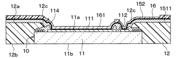
本実施形態の半導体装置1は、例えば図1に示すように、半導体素子11と、封止材12と、第1導体部13と、第2導体部14と、半導体素子11の上にて、半導体素子11の外郭内側から外側まで延設された延設配線152を有する再配線層15とを備える。半導体素子11は、表面11aに第1電極パッド111、複数の第2電極パッド112、電界緩和層113および素子上絶縁膜114を備え、第1電極パッド111に第1導体部13が接続され、第2電極パッド112に第2導体部14が接続されている。延設配線152は、第2導体部14から半導体素子11の外郭外側にまで延設されると共に、その先端付近の一部の領域が封止材12から露出している。この半導体装置1は、半導体素子11の表面11aの一部が封止材12により覆われ、封止材12の一面12a上に延設配線152を含む再配線層15が形成されたファンアウトパッケージ構造(以下「FOP構造」という)である。
次に、本実施形態の半導体装置1の製造方法の一例について、図3A~図3Jを参照して説明する。
〔製造方法の変形例〕
上記の製造方法は、あくまで一例であり、これに限定されるものではない。例えば、被覆部161および延設配線152を電解メッキに代えて、スクリーン印刷法により形成してもよい。
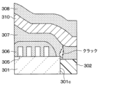
ここで、本実施形態の半導体装置1において、延設配線152と半導体素子11との短絡が抑制される理由について、封止材302により表面が覆われていない半導体装置300(以下、単に「半導体装置300」という)を示す図5、図6を参照して説明する。
〔半導体モジュールの構成例〕
次に、本実施形態の半導体装置1を用いた半導体モジュールの一例については、図7を参照して説明する。図7では、後述する第2ヒートシンク3のうち別断面において外部に接続される配線部分を破線で示している。
第2実施形態の半導体装置1について、図9を参照して説明する。
次に、本実施形態の半導体装置1の製造方法の一例について、図10A~図10Kを参照して説明する。ここでは、上記第1実施形態の半導体装置1の製造工程とは異なる相違部分について主に説明する。
上記では、内壁面12cの断面形状が湾曲した形状である例について説明したが、これに限定されるものでない。内壁面12cは、一面12aと半導体素子11の露出部分とのなす段差が緩やかに変化する形状であればよく、例えば図13に示すように、一面12aと内壁面12cとのなす交差角度θが鈍角となるテーパ形状であってもよい。つまり、内壁面12cは、封止材12の一面12aと交差する上端部分を角部として角部が鈍角となる断面形状とされた場合であっても、絶縁層151の段切れを抑制できる。この場合であっても、絶縁層151の第1層1511が封止材12の角部に追従でき、封止材12の角部で局所的に薄くなったり、角部が第1層1511から露出したりすることが抑制され、延設配線152の段切れも抑制できる。
第3実施形態の半導体装置1について、図14~図16Bを参照して説明する。
〔製造方法〕
次に、本実施形態の半導体装置1の製造方法の一例について、図16A、図16Bを参照して説明する。ここでは、上記第1実施形態とは異なる製造工程について主に説明する。
本発明は、実施例に準拠して記述されたが、本発明は当該実施例や構造に限定されるものではないと理解される。本発明は、様々な変形例や均等範囲内の変形をも包含する。加えて、様々な組み合わせや形態、さらには、それらの一要素のみ、それ以上、あるいはそれ以下、を含む他の組み合わせや形態をも、本発明の範疇や思想範囲に入るものである。
111・・・第1電極パッド、112・・・第2電極パッド、12c・・・内壁面、
114・・・素子上絶縁膜、12・・・封止材、12a・・・一面、
13・・・第1導体部、14・・・第2導体部、151・・・絶縁層、
1511・・・第1層、1512・・・第2層、152・・・延設配線、
153・・・第1外部電極、154・・・第2外部電極、2・・・第1放熱部材、
2a・・・上面、3・・・第2放熱部材、3b・・・下面、4・・・リードフレーム、
5・・・接合材、6・・・封止材、7・・・伝熱絶縁基板、71・・・電気伝導部、
72・・・絶縁部、73・・・熱伝導部、19・・・導電部材、191・・・厚肉部、
192・・・第1薄肉部、193・・・中肉部、194・・・第2薄肉部
Claims (14)
- 表面(11a)に第1電極パッド(111)および複数の第2電極パッド(112)を有し、前記表面と裏面(11b)とを繋ぐ方向に電流が生じる半導体素子(11)と、
絶縁性の樹脂材料で構成され、前記半導体素子の前記表面の一部および側面(11c)を覆う封止材(12)と、
前記半導体素子の上であって、前記封止材の内部または前記封止材の上に配置され、前記第2電極パッドと電気的に接続されると共に、前記半導体素子の外郭の内側から外側まで延設されている延設配線(152)と、を備え、
前記封止材のうち前記半導体素子の前記表面の側を覆う面を一面(12a)として、前記一面は、前記封止材とは異なる絶縁性の樹脂材料で構成された絶縁層(151)により覆われている、半導体装置。 - 前記第1電極パッドに接続されると共に、前記第1電極パッドの真上に向かって延設され、前記封止材から露出する第1導体部(13、181)と、
前記第2電極パッドに接続されると共に、前記第2電極パッドの上部に向かって延設され、前記封止材から露出する第2導体部(14、182)と、をさらに備え、
前記延設配線は、前記第2導体部に接続されている、請求項1に記載の半導体装置。 - 前記第1導体部は、単一の部材で構成され、前記第1電極パッドに接続された側の面とは反対側の面が外部に露出しており、
前記第2導体部は、一部が前記延設配線であり、前記第1導体部と同一の材料によりなる単一の部材で構成されると共に、前記第2電極パッドに接続された側の面とは反対側の面が外部に露出している、請求項2に記載の半導体装置。 - 前記第1電極パッドに電気的に接続され、前記第1電極パッドとは反対側において外部に露出する電極部分を第1外部電極(153)とし、前記第2電極パッドに電気的に接続され、前記第2電極パッドとは反対側において外部に露出する部分を第2外部電極(154)として、
前記第1外部電極は、前記第2外部電極と距離を隔てて配置され、前記第2外部電極よりも平面サイズが大きい、請求項1ないし3のいずれか1つに記載の半導体装置。 - 前記延設配線は、Cu、Al、Ti、Au、Ag、Pd、W、Ni、Zn、Pbのうちいずれか1つを主成分とする導電性材料により構成されている、請求項1ないし4のいずれか1つに記載の半導体装置。
- 前記絶縁層のうち前記延設配線よりも前記一面の側の部分を第1層(1511)として、
前記第1層の厚みは、前記絶縁層のうち前記延設配線よりも上に位置する部分の厚みよりも大きい、請求項1ないし5のいずれか1つに記載の半導体装置。 - 表面(11a)に第1電極パッド(111)および複数の第2電極パッド(112)を有し、前記表面と裏面(11b)とを繋ぐ方向に電流が生じる半導体素子(11)と、
絶縁性の樹脂材料で構成され、前記半導体素子の前記表面の一部および側面(11c)を覆う封止材(12)と、
前記半導体素子の上であって、前記封止材の内部または前記封止材の上に配置され、前記第2電極パッドと電気的に接続されると共に、前記半導体素子の外郭の内側から外側まで延設されている延設配線(152)と、
前記第1電極パッドに接続されると共に、前記第1電極パッドの真上に向かって延設され、前記封止材から露出する第1導体部(13、181)と、
前記第2電極パッドに接続されると共に、前記第2電極パッドの上部に向かって延設され、前記封止材から露出する第2導体部(14、182)と、を備え、
前記延設配線は、前記第2導体部に接続されており、
前記第2導体部は、一部が前記延設配線であり、前記第1導体部とは異なる導電性材料から構成されている、半導体装置。 - 表面(11a)に第1電極パッド(111)および複数の第2電極パッド(112)を有し、前記表面と裏面(11b)とを繋ぐ方向に電流が生じる半導体素子(11)と、
絶縁性の樹脂材料で構成され、前記半導体素子の前記表面の一部および側面(11c)を覆う封止材(12)と、
前記半導体素子の上であって、前記封止材の内部または前記封止材の上に配置され、前記第2電極パッドと電気的に接続されると共に、前記半導体素子の外郭の内側から外側まで延設されている延設配線(152)と、を備え、
前記封止材のうち前記半導体素子の前記表面の側を覆う面を一面(12a)とし、前記半導体素子の前記表面の上に位置する面であって、前記一面に繋がる面を内壁面(12c)として、
前記内壁面のうち前記一面と交差する上端部分の断面形状は、湾曲した曲面形状である、半導体装置。 - 表面(11a)に第1電極パッド(111)および複数の第2電極パッド(112)を有し、前記表面と裏面(11b)とを繋ぐ方向に電流が生じる半導体素子(11)と、
絶縁性の樹脂材料で構成され、前記半導体素子の前記表面の一部および側面(11c)を覆う封止材(12)と、
前記半導体素子の上であって、前記封止材の内部または前記封止材の上に配置され、前記第2電極パッドと電気的に接続されると共に、前記半導体素子の外郭の内側から外側まで延設されている延設配線(152)と、を備え、
前記封止材のうち前記半導体素子の前記表面の側を覆う面を一面(12a)とし、前記半導体素子の前記表面の上に位置する面であって、前記一面に繋がる面を内壁面(12c)とし、前記内壁面と前記一面と交差する上端部分の角度を交差角度(θ)として、
前記内壁面の断面形状は、前記交差角度が鈍角となる形状である、半導体装置。 - 表面(11a)に少なくとも1つ以上の第1電極パッド(111)および少なくとも1つ以上の第2電極パッド(112)を有し、前記表面と裏面(11b)とを繋ぐ方向に電流が生じる半導体素子(11)と、絶縁性の樹脂材料で構成され、前記表面の一部を含む前記半導体素子の周囲を覆う第1の封止材(12)と、前記半導体素子の上であって、前記第1の封止材の内部または前記第1の封止材の上に配置され、前記第2電極パッドと電気的に接続されると共に、前記半導体素子の外郭の内側から外側まで延設されている延設配線(152)と、を備える半導体装置(1)と、
前記半導体装置のうち前記第1の封止材から露出する前記裏面に接合材(5)を介して接続される第1放熱部材(2)と、
前記半導体装置のうち前記第1電極パッドに前記接合材を介して電気的に接続される第2放熱部材(3)と、
前記半導体装置のうち前記延設配線に前記接合材を介して電気的に接続されるリードフレーム(4)と、
前記半導体装置、前記第1放熱部材の一部、前記第2放熱部材の一部および前記リードフレームの一部を覆う第2の封止材(6)と、を備える、半導体モジュール。 - 前記半導体装置の一部は、前記第2放熱部材の外郭よりも外側に位置する露出領域であり、
前記リードフレームは、前記露出領域において前記接合材を介して前記延設配線に電気的に接続されている、請求項10に記載の半導体モジュール。 - 前記第1放熱部材のうち前記半導体装置に向き合う面とは反対面である上面(2a)は、前記第2の封止材から露出しており、
前記第2放熱部材のうち前記半導体装置に向き合う面とは反対面である下面(3b)は、前記第2の封止材から露出している、請求項10または11に記載の半導体モジュール。 - 前記第1放熱部材および前記第2放熱部材は、一部または全部が、電気伝導部(71)と、絶縁部(72)と、熱伝導部(73)とがこの順に積層された伝熱絶縁基板(7)であり、前記電気伝導部が前記半導体装置に接続されている、請求項10ないし12のいずれか1つに記載の半導体モジュール。
- ファンアウトパッケージ構造の半導体装置の製造方法であって、
表面(11a)に少なくとも1つ以上の第1電極パッド(111)および少なくとも1つ以上の第2電極パッド(112)を備える半導体素子(11)を用意することと、
厚肉部(191)と、前記厚肉部の上端から外部に向かって延設され、前記厚肉部よりも厚みが小さい第1薄肉部(192)と、前記第1薄肉部の先端に設けられ、前記厚肉部よりも厚みが小さく、かつ前記第1薄肉部よりも厚みが大きい中肉部(193)と、前記中肉部から前記厚肉部の下端の側に向かって延設され、前記厚肉部よりも厚みが小さい第2薄肉部(194)とを備える導電部材(19)を用意することと、
前記半導体素子の裏面(11b)を支持基板(200)に貼り付けることと、
前記半導体素子の前記第1電極パッドに前記導電部材のうち前記厚肉部の下端側の面を接続し、前記半導体素子の前記第2電極パッドに前記導電部材のうち前記第2薄肉部の先端を接続することと、
前記導電部材が接続され、前記支持基板に貼り付けられた前記半導体素子を前記導電部材ごと覆う封止材(12)を形成することと、
前記封止材のうち前記導電部材を覆う側の面から前記封止材を除去し、前記導電部材の前記厚肉部および前記中肉部を前記封止材から露出させることと、を含み、
前記封止材を形成することにおいては、絶縁性の樹脂材料を用い、
前記封止材を除去することにおいては、前記導電部材のうち前記第1薄肉部を除去し、前記厚肉部と、前記中肉部および前記第2薄肉部とを分離させる、半導体装置の製造方法。
Priority Applications (4)
| Application Number | Priority Date | Filing Date | Title |
|---|---|---|---|
| JP2020098220A JP7516883B2 (ja) | 2020-06-05 | 2020-06-05 | 半導体装置、半導体モジュールおよび半導体装置の製造方法 |
| CN202180040056.8A CN115699296A (zh) | 2020-06-05 | 2021-05-21 | 半导体装置、半导体模组及半导体装置的制造方法 |
| PCT/JP2021/019433 WO2021246204A1 (ja) | 2020-06-05 | 2021-05-21 | 半導体装置、半導体モジュールおよび半導体装置の製造方法 |
| US18/059,748 US20230093554A1 (en) | 2020-06-05 | 2022-11-29 | Semiconductor device, semiconductor module, and method for manufacturing semiconductor device |
Applications Claiming Priority (1)
| Application Number | Priority Date | Filing Date | Title |
|---|---|---|---|
| JP2020098220A JP7516883B2 (ja) | 2020-06-05 | 2020-06-05 | 半導体装置、半導体モジュールおよび半導体装置の製造方法 |
Publications (3)
| Publication Number | Publication Date |
|---|---|
| JP2021190670A JP2021190670A (ja) | 2021-12-13 |
| JP2021190670A5 JP2021190670A5 (ja) | 2022-05-19 |
| JP7516883B2 true JP7516883B2 (ja) | 2024-07-17 |
Family
ID=78831005
Family Applications (1)
| Application Number | Title | Priority Date | Filing Date |
|---|---|---|---|
| JP2020098220A Active JP7516883B2 (ja) | 2020-06-05 | 2020-06-05 | 半導体装置、半導体モジュールおよび半導体装置の製造方法 |
Country Status (4)
| Country | Link |
|---|---|
| US (1) | US20230093554A1 (ja) |
| JP (1) | JP7516883B2 (ja) |
| CN (1) | CN115699296A (ja) |
| WO (1) | WO2021246204A1 (ja) |
Citations (6)
| Publication number | Priority date | Publication date | Assignee | Title |
|---|---|---|---|---|
| JP2010287651A (ja) | 2009-06-10 | 2010-12-24 | Nissan Motor Co Ltd | 半導体装置 |
| JP2011181879A (ja) | 2010-02-04 | 2011-09-15 | Denso Corp | 半導体装置およびその製造方法 |
| JP2013172105A (ja) | 2012-02-22 | 2013-09-02 | Toyota Motor Corp | 半導体モジュール |
| JP2014157927A (ja) | 2013-02-15 | 2014-08-28 | Denso Corp | 半導体装置及びその製造方法 |
| US20200176348A1 (en) | 2018-11-30 | 2020-06-04 | Delta Electronics Int'l (Singapore) Pte Ltd | Package structure and power module using same |
| WO2020189508A1 (ja) | 2019-03-19 | 2020-09-24 | 株式会社デンソー | 半導体モジュールおよびこれに用いられる半導体装置 |
Family Cites Families (2)
| Publication number | Priority date | Publication date | Assignee | Title |
|---|---|---|---|---|
| JP2020077857A (ja) * | 2018-09-28 | 2020-05-21 | 太陽誘電株式会社 | モジュールおよびその製造方法 |
| JP2020088107A (ja) * | 2018-11-21 | 2020-06-04 | トヨタ自動車株式会社 | 半導体モジュール |
-
2020
- 2020-06-05 JP JP2020098220A patent/JP7516883B2/ja active Active
-
2021
- 2021-05-21 WO PCT/JP2021/019433 patent/WO2021246204A1/ja active Application Filing
- 2021-05-21 CN CN202180040056.8A patent/CN115699296A/zh active Pending
-
2022
- 2022-11-29 US US18/059,748 patent/US20230093554A1/en active Pending
Patent Citations (6)
| Publication number | Priority date | Publication date | Assignee | Title |
|---|---|---|---|---|
| JP2010287651A (ja) | 2009-06-10 | 2010-12-24 | Nissan Motor Co Ltd | 半導体装置 |
| JP2011181879A (ja) | 2010-02-04 | 2011-09-15 | Denso Corp | 半導体装置およびその製造方法 |
| JP2013172105A (ja) | 2012-02-22 | 2013-09-02 | Toyota Motor Corp | 半導体モジュール |
| JP2014157927A (ja) | 2013-02-15 | 2014-08-28 | Denso Corp | 半導体装置及びその製造方法 |
| US20200176348A1 (en) | 2018-11-30 | 2020-06-04 | Delta Electronics Int'l (Singapore) Pte Ltd | Package structure and power module using same |
| WO2020189508A1 (ja) | 2019-03-19 | 2020-09-24 | 株式会社デンソー | 半導体モジュールおよびこれに用いられる半導体装置 |
Also Published As
| Publication number | Publication date |
|---|---|
| US20230093554A1 (en) | 2023-03-23 |
| JP2021190670A (ja) | 2021-12-13 |
| WO2021246204A1 (ja) | 2021-12-09 |
| CN115699296A (zh) | 2023-02-03 |
Similar Documents
| Publication | Publication Date | Title |
|---|---|---|
| JP5141076B2 (ja) | 半導体装置 | |
| US5874784A (en) | Semiconductor device having external connection terminals provided on an interconnection plate and fabrication process therefor | |
| JP3152180B2 (ja) | 半導体装置及びその製造方法 | |
| JP3189703B2 (ja) | 半導体装置及びその製造方法 | |
| JP3684978B2 (ja) | 半導体装置およびその製造方法ならびに電子機器 | |
| JP3390661B2 (ja) | パワーモジュール | |
| JPH02285646A (ja) | 半導体装置 | |
| CN110178202B (zh) | 半导体装置及其制造方法 | |
| US20030122237A1 (en) | Semiconductor device | |
| JP2014022505A (ja) | 半導体装置およびその製造方法 | |
| JP2007157844A (ja) | 半導体装置、および半導体装置の製造方法 | |
| JP7088224B2 (ja) | 半導体モジュールおよびこれに用いられる半導体装置 | |
| JP7117960B2 (ja) | パワーモジュール用基板およびパワーモジュール | |
| JP3685659B2 (ja) | 半導体装置の製造方法 | |
| JP2021007182A (ja) | 半導体装置及びその製造方法 | |
| JP7516883B2 (ja) | 半導体装置、半導体モジュールおよび半導体装置の製造方法 | |
| JP7472806B2 (ja) | 半導体装置、パワーモジュール及び半導体装置の製造方法 | |
| WO2020189508A1 (ja) | 半導体モジュールおよびこれに用いられる半導体装置 | |
| WO2022009705A1 (ja) | 半導体装置および半導体モジュール | |
| JP2016219707A (ja) | 半導体装置及びその製造方法 | |
| JP3314574B2 (ja) | 半導体装置の製造方法 | |
| JP2008235492A (ja) | 半導体装置および半導体装置の製造方法 | |
| JP2004273561A (ja) | 半導体装置及びその製造方法 | |
| JP4356196B2 (ja) | 半導体装置組立体 | |
| JP2000100864A (ja) | 半導体装置及びその組立体 |
Legal Events
| Date | Code | Title | Description |
|---|---|---|---|
| A521 | Request for written amendment filed |
Free format text: JAPANESE INTERMEDIATE CODE: A523 Effective date: 20220511 |
|
| A621 | Written request for application examination |
Free format text: JAPANESE INTERMEDIATE CODE: A621 Effective date: 20230403 |
|
| TRDD | Decision of grant or rejection written | ||
| A01 | Written decision to grant a patent or to grant a registration (utility model) |
Free format text: JAPANESE INTERMEDIATE CODE: A01 Effective date: 20240604 |
|
| A61 | First payment of annual fees (during grant procedure) |
Free format text: JAPANESE INTERMEDIATE CODE: A61 Effective date: 20240617 |
|
| R150 | Certificate of patent or registration of utility model |
Ref document number: 7516883 Country of ref document: JP Free format text: JAPANESE INTERMEDIATE CODE: R150 |