WO2018198330A1 - キャパシタ装置とその製造方法 - Google Patents
キャパシタ装置とその製造方法 Download PDFInfo
- Publication number
- WO2018198330A1 WO2018198330A1 PCT/JP2017/016977 JP2017016977W WO2018198330A1 WO 2018198330 A1 WO2018198330 A1 WO 2018198330A1 JP 2017016977 W JP2017016977 W JP 2017016977W WO 2018198330 A1 WO2018198330 A1 WO 2018198330A1
- Authority
- WO
- WIPO (PCT)
- Prior art keywords
- cell
- capacitor device
- capacitor
- terminals
- electrode
- Prior art date
Links
- 239000003990 capacitor Substances 0.000 title claims abstract description 437
- 238000004519 manufacturing process Methods 0.000 title claims description 68
- 210000004027 cell Anatomy 0.000 claims description 386
- 239000004020 conductor Substances 0.000 claims description 116
- 239000000758 substrate Substances 0.000 claims description 74
- 239000004065 semiconductor Substances 0.000 claims description 68
- 229910052751 metal Inorganic materials 0.000 claims description 65
- 239000002184 metal Substances 0.000 claims description 65
- 238000000034 method Methods 0.000 claims description 31
- VYPSYNLAJGMNEJ-UHFFFAOYSA-N Silicium dioxide Chemical compound O=[Si]=O VYPSYNLAJGMNEJ-UHFFFAOYSA-N 0.000 claims description 30
- XUIMIQQOPSSXEZ-UHFFFAOYSA-N Silicon Chemical compound [Si] XUIMIQQOPSSXEZ-UHFFFAOYSA-N 0.000 claims description 30
- 229910052710 silicon Inorganic materials 0.000 claims description 30
- 239000010703 silicon Substances 0.000 claims description 30
- 229910052814 silicon oxide Inorganic materials 0.000 claims description 30
- 239000000463 material Substances 0.000 claims description 16
- 238000002161 passivation Methods 0.000 claims description 15
- 210000004460 N cell Anatomy 0.000 claims description 13
- 230000015556 catabolic process Effects 0.000 claims description 6
- 229910018072 Al 2 O 3 Inorganic materials 0.000 claims description 3
- 229910010413 TiO 2 Inorganic materials 0.000 claims description 3
- 239000010410 layer Substances 0.000 description 35
- 238000010586 diagram Methods 0.000 description 17
- 150000004767 nitrides Chemical class 0.000 description 16
- 239000011229 interlayer Substances 0.000 description 10
- 230000008569 process Effects 0.000 description 10
- 238000005516 engineering process Methods 0.000 description 9
- CIWBSHSKHKDKBQ-JLAZNSOCSA-N Ascorbic acid Chemical compound OC[C@H](O)[C@H]1OC(=O)C(O)=C1O CIWBSHSKHKDKBQ-JLAZNSOCSA-N 0.000 description 7
- 230000004888 barrier function Effects 0.000 description 7
- 230000000694 effects Effects 0.000 description 5
- 238000005530 etching Methods 0.000 description 5
- 238000005498 polishing Methods 0.000 description 5
- 238000003491 array Methods 0.000 description 4
- 230000008859 change Effects 0.000 description 3
- 229920002120 photoresistant polymer Polymers 0.000 description 3
- 230000008901 benefit Effects 0.000 description 2
- 238000007796 conventional method Methods 0.000 description 2
- 238000013461 design Methods 0.000 description 2
- 239000003989 dielectric material Substances 0.000 description 2
- 230000004048 modification Effects 0.000 description 2
- 238000012986 modification Methods 0.000 description 2
- 230000009467 reduction Effects 0.000 description 2
- WFKWXMTUELFFGS-UHFFFAOYSA-N tungsten Chemical compound [W] WFKWXMTUELFFGS-UHFFFAOYSA-N 0.000 description 2
- 229910052721 tungsten Inorganic materials 0.000 description 2
- 239000010937 tungsten Substances 0.000 description 2
- 229910000577 Silicon-germanium Inorganic materials 0.000 description 1
- LEVVHYCKPQWKOP-UHFFFAOYSA-N [Si].[Ge] Chemical compound [Si].[Ge] LEVVHYCKPQWKOP-UHFFFAOYSA-N 0.000 description 1
- 239000003985 ceramic capacitor Substances 0.000 description 1
- 239000011796 hollow space material Substances 0.000 description 1
- 230000010354 integration Effects 0.000 description 1
- 238000007521 mechanical polishing technique Methods 0.000 description 1
- 238000000059 patterning Methods 0.000 description 1
- 230000000149 penetrating effect Effects 0.000 description 1
- 238000011165 process development Methods 0.000 description 1
- 230000001681 protective effect Effects 0.000 description 1
- 229910000679 solder Inorganic materials 0.000 description 1
- 239000000126 substance Substances 0.000 description 1
Images


Classifications
-
- H—ELECTRICITY
- H01—ELECTRIC ELEMENTS
- H01L—SEMICONDUCTOR DEVICES NOT COVERED BY CLASS H10
- H01L28/00—Passive two-terminal components without a potential-jump or surface barrier for integrated circuits; Details thereof; Multistep manufacturing processes therefor
- H01L28/40—Capacitors
- H01L28/60—Electrodes
- H01L28/82—Electrodes with an enlarged surface, e.g. formed by texturisation
- H01L28/90—Electrodes with an enlarged surface, e.g. formed by texturisation having vertical extensions
-
- H—ELECTRICITY
- H01—ELECTRIC ELEMENTS
- H01L—SEMICONDUCTOR DEVICES NOT COVERED BY CLASS H10
- H01L21/00—Processes or apparatus adapted for the manufacture or treatment of semiconductor or solid state devices or of parts thereof
- H01L21/02—Manufacture or treatment of semiconductor devices or of parts thereof
- H01L21/04—Manufacture or treatment of semiconductor devices or of parts thereof the devices having potential barriers, e.g. a PN junction, depletion layer or carrier concentration layer
- H01L21/18—Manufacture or treatment of semiconductor devices or of parts thereof the devices having potential barriers, e.g. a PN junction, depletion layer or carrier concentration layer the devices having semiconductor bodies comprising elements of Group IV of the Periodic Table or AIIIBV compounds with or without impurities, e.g. doping materials
- H01L21/28—Manufacture of electrodes on semiconductor bodies using processes or apparatus not provided for in groups H01L21/20 - H01L21/268
- H01L21/283—Deposition of conductive or insulating materials for electrodes conducting electric current
-
- H—ELECTRICITY
- H01—ELECTRIC ELEMENTS
- H01L—SEMICONDUCTOR DEVICES NOT COVERED BY CLASS H10
- H01L21/00—Processes or apparatus adapted for the manufacture or treatment of semiconductor or solid state devices or of parts thereof
- H01L21/02—Manufacture or treatment of semiconductor devices or of parts thereof
- H01L21/04—Manufacture or treatment of semiconductor devices or of parts thereof the devices having potential barriers, e.g. a PN junction, depletion layer or carrier concentration layer
- H01L21/18—Manufacture or treatment of semiconductor devices or of parts thereof the devices having potential barriers, e.g. a PN junction, depletion layer or carrier concentration layer the devices having semiconductor bodies comprising elements of Group IV of the Periodic Table or AIIIBV compounds with or without impurities, e.g. doping materials
- H01L21/30—Treatment of semiconductor bodies using processes or apparatus not provided for in groups H01L21/20 - H01L21/26
- H01L21/31—Treatment of semiconductor bodies using processes or apparatus not provided for in groups H01L21/20 - H01L21/26 to form insulating layers thereon, e.g. for masking or by using photolithographic techniques; After treatment of these layers; Selection of materials for these layers
- H01L21/3205—Deposition of non-insulating-, e.g. conductive- or resistive-, layers on insulating layers; After-treatment of these layers
- H01L21/321—After treatment
- H01L21/3213—Physical or chemical etching of the layers, e.g. to produce a patterned layer from a pre-deposited extensive layer
- H01L21/32139—Physical or chemical etching of the layers, e.g. to produce a patterned layer from a pre-deposited extensive layer using masks
-
- H—ELECTRICITY
- H01—ELECTRIC ELEMENTS
- H01L—SEMICONDUCTOR DEVICES NOT COVERED BY CLASS H10
- H01L23/00—Details of semiconductor or other solid state devices
- H01L23/52—Arrangements for conducting electric current within the device in operation from one component to another, i.e. interconnections, e.g. wires, lead frames
- H01L23/522—Arrangements for conducting electric current within the device in operation from one component to another, i.e. interconnections, e.g. wires, lead frames including external interconnections consisting of a multilayer structure of conductive and insulating layers inseparably formed on the semiconductor body
- H01L23/5226—Via connections in a multilevel interconnection structure
-
- H—ELECTRICITY
- H01—ELECTRIC ELEMENTS
- H01L—SEMICONDUCTOR DEVICES NOT COVERED BY CLASS H10
- H01L23/00—Details of semiconductor or other solid state devices
- H01L23/52—Arrangements for conducting electric current within the device in operation from one component to another, i.e. interconnections, e.g. wires, lead frames
- H01L23/522—Arrangements for conducting electric current within the device in operation from one component to another, i.e. interconnections, e.g. wires, lead frames including external interconnections consisting of a multilayer structure of conductive and insulating layers inseparably formed on the semiconductor body
- H01L23/528—Geometry or layout of the interconnection structure
-
- H—ELECTRICITY
- H01—ELECTRIC ELEMENTS
- H01L—SEMICONDUCTOR DEVICES NOT COVERED BY CLASS H10
- H01L27/00—Devices consisting of a plurality of semiconductor or other solid-state components formed in or on a common substrate
- H01L27/02—Devices consisting of a plurality of semiconductor or other solid-state components formed in or on a common substrate including semiconductor components specially adapted for rectifying, oscillating, amplifying or switching and having potential barriers; including integrated passive circuit elements having potential barriers
- H01L27/04—Devices consisting of a plurality of semiconductor or other solid-state components formed in or on a common substrate including semiconductor components specially adapted for rectifying, oscillating, amplifying or switching and having potential barriers; including integrated passive circuit elements having potential barriers the substrate being a semiconductor body
- H01L27/08—Devices consisting of a plurality of semiconductor or other solid-state components formed in or on a common substrate including semiconductor components specially adapted for rectifying, oscillating, amplifying or switching and having potential barriers; including integrated passive circuit elements having potential barriers the substrate being a semiconductor body including only semiconductor components of a single kind
- H01L27/0805—Capacitors only
-
- H—ELECTRICITY
- H01—ELECTRIC ELEMENTS
- H01L—SEMICONDUCTOR DEVICES NOT COVERED BY CLASS H10
- H01L27/00—Devices consisting of a plurality of semiconductor or other solid-state components formed in or on a common substrate
- H01L27/02—Devices consisting of a plurality of semiconductor or other solid-state components formed in or on a common substrate including semiconductor components specially adapted for rectifying, oscillating, amplifying or switching and having potential barriers; including integrated passive circuit elements having potential barriers
- H01L27/04—Devices consisting of a plurality of semiconductor or other solid-state components formed in or on a common substrate including semiconductor components specially adapted for rectifying, oscillating, amplifying or switching and having potential barriers; including integrated passive circuit elements having potential barriers the substrate being a semiconductor body
- H01L27/10—Devices consisting of a plurality of semiconductor or other solid-state components formed in or on a common substrate including semiconductor components specially adapted for rectifying, oscillating, amplifying or switching and having potential barriers; including integrated passive circuit elements having potential barriers the substrate being a semiconductor body including a plurality of individual components in a repetitive configuration
- H01L27/101—Devices consisting of a plurality of semiconductor or other solid-state components formed in or on a common substrate including semiconductor components specially adapted for rectifying, oscillating, amplifying or switching and having potential barriers; including integrated passive circuit elements having potential barriers the substrate being a semiconductor body including a plurality of individual components in a repetitive configuration including resistors or capacitors only
-
- H—ELECTRICITY
- H01—ELECTRIC ELEMENTS
- H01L—SEMICONDUCTOR DEVICES NOT COVERED BY CLASS H10
- H01L28/00—Passive two-terminal components without a potential-jump or surface barrier for integrated circuits; Details thereof; Multistep manufacturing processes therefor
- H01L28/40—Capacitors
- H01L28/60—Electrodes
- H01L28/75—Electrodes comprising two or more layers, e.g. comprising a barrier layer and a metal layer
-
- H—ELECTRICITY
- H01—ELECTRIC ELEMENTS
- H01L—SEMICONDUCTOR DEVICES NOT COVERED BY CLASS H10
- H01L28/00—Passive two-terminal components without a potential-jump or surface barrier for integrated circuits; Details thereof; Multistep manufacturing processes therefor
- H01L28/40—Capacitors
- H01L28/60—Electrodes
- H01L28/82—Electrodes with an enlarged surface, e.g. formed by texturisation
- H01L28/90—Electrodes with an enlarged surface, e.g. formed by texturisation having vertical extensions
- H01L28/91—Electrodes with an enlarged surface, e.g. formed by texturisation having vertical extensions made by depositing layers, e.g. by depositing alternating conductive and insulating layers
-
- H—ELECTRICITY
- H10—SEMICONDUCTOR DEVICES; ELECTRIC SOLID-STATE DEVICES NOT OTHERWISE PROVIDED FOR
- H10B—ELECTRONIC MEMORY DEVICES
- H10B12/00—Dynamic random access memory [DRAM] devices
- H10B12/01—Manufacture or treatment
- H10B12/02—Manufacture or treatment for one transistor one-capacitor [1T-1C] memory cells
- H10B12/03—Making the capacitor or connections thereto
-
- H—ELECTRICITY
- H10—SEMICONDUCTOR DEVICES; ELECTRIC SOLID-STATE DEVICES NOT OTHERWISE PROVIDED FOR
- H10B—ELECTRONIC MEMORY DEVICES
- H10B12/00—Dynamic random access memory [DRAM] devices
- H10B12/30—DRAM devices comprising one-transistor - one-capacitor [1T-1C] memory cells
Definitions
- the present invention relates to a capacitor device including one or a plurality of capacitor cells formed on a semiconductor substrate, and a manufacturing method thereof.
- a capacitor device including one or a plurality of capacitor cells formed on a semiconductor substrate using a semiconductor process technology is known. Such a capacitor device is required to satisfy various requirements such as an increase in capacity, a reduction in size, a reduction in manufacturing cost, and ease of design change.
- Patent Document 1 discloses a trench capacitor having a structure formed in a direction perpendicular to the surface of a semiconductor substrate.
- Capacitor devices are required to reduce the diameter and spacing of terminals (solder balls, etc.) and the thickness of the capacitor device for further circuit integration.
- the trench capacitor as in Patent Document 1, since the trench capacitor is formed in the silicon substrate, it is necessary to polish the surface of the silicon substrate in the manufacturing process so that the capacitor portion remains. Therefore, the thickness (depth) of the silicon substrate that can be reduced by polishing is limited. In addition, the depth of trench capacitors is increasing with the miniaturization of semiconductor process technology, and there is a trench capacitor having a depth exceeding 10 ⁇ m. Therefore, as the depth of the trench capacitor increases, the final capacitor device thickness also increases. Accordingly, there is a need for a capacitor device having a reduced thickness compared to the conventional one without being subject to such restrictions.
- An object of the present invention is to provide a capacitor device including one or a plurality of capacitor cells formed on a semiconductor substrate, and having a reduced thickness compared to the conventional one.
- Another object of the present invention is a capacitor device including one or a plurality of capacitor cells formed on a semiconductor substrate, which can be manufactured by changing the characteristics of the capacitor described above at a lower cost than in the past. Is required.
- an object of the present invention is to provide a method for manufacturing such a capacitor device.
- the capacitor device includes: A capacitor device including a plurality of capacitor cells formed on a rectangular semiconductor substrate having sides extending along a first direction and a second direction orthogonal to each other,
- the capacitor device includes: A plurality of first electrodes including a portion formed in a first layer of the semiconductor substrate, arranged in a first period in the first direction, and second in the second direction; A plurality of first electrodes arranged in a period; A plurality of second electrodes including a portion formed in a second layer different from the first layer of the semiconductor substrate, disposed in the first direction at the first period, and A plurality of second electrodes arranged in the second direction at the second period, Each of the second electrodes is arranged so as to be shifted from the first electrode by half the length of the first period in the first direction, and the second electrode is moved in the second direction.
- Each first electrode and each second electrode are partially coupled to each other and capacitively coupled to each other, and each pair of the first and second electrodes coupled to each other and capacitively coupled is a capacitor cell.
- the capacitor device includes: A plurality of first cell terminals including a portion formed in a third layer different from the first and second layers of the semiconductor substrate, the first cell terminals being arranged in the first direction at the first period; A plurality of first cell terminals arranged in the second direction at the second period and electrically connected to the plurality of first electrodes, respectively.
- a plurality of second cell terminals including a portion formed in a third layer of the semiconductor substrate, arranged at the first period in the first direction, and the second cell terminal in the second direction; And a plurality of second cell terminals electrically connected to the plurality of second electrodes, respectively.
- the second layer is located between the first and third layers;
- Each of the second cell terminals is shifted from the first cell terminal by half the length of the first period in the first direction, and in the second direction.
- the second period is shifted by half the length of the second period.
- a capacitor device is the capacitor device according to the first aspect, The capacitor device further includes at least two external terminals, and each external terminal is electrically connected to a part of the plurality of cell terminals including the plurality of first cell terminals and the plurality of second cell terminals. Connected.
- a capacitor device is the capacitor device according to the second aspect,
- the plurality of cell terminals respectively extend in the first direction or the second direction, and form a plurality of cell terminal rows adjacent to each other in the extending direction;
- the capacitor device includes first and second external terminals each having a comb shape, Each of the first and second external terminals includes a plurality of first portions electrically connected to every 2N cell terminal rows of the plurality of cell terminal rows when N is an integer. And a second portion connecting the first portions to each other, and the first portions of the first external terminals and the first portions of the second external terminals are fitted to each other. Formed into The first and second external terminals are arranged such that every N cell terminal rows of the plurality of cell terminal rows are electrically connected to the first and second external terminals alternately.
- a capacitor device is the capacitor device according to the second aspect,
- the plurality of cell terminals respectively extend in the first direction or the second direction, and form a plurality of cell terminal rows adjacent to each other in the extending direction;
- the capacitor device includes a first external terminal having a fishbone shape, and second and third external terminals each having a comb shape, A plurality of first portions electrically connected to every 2N cell terminal rows of the plurality of cell terminal rows when N is an integer; and A second portion connecting the first portions of the first external terminals to each other at the center of the first portions of the external terminals;
- the second external terminal includes a plurality of first portions electrically connected to a part of the plurality of cell terminals included in every 2N cell terminal rows of the plurality of cell terminal rows.
- a second portion that connects each first portion of the second external terminal to each other, and the second external terminal is a first portion based on the second portion of the first external terminal.
- the third external terminal includes a plurality of first portions electrically connected to a part of a plurality of cell terminals included in every 2N cell terminal rows of the plurality of cell terminal rows. And a second portion that connects each first portion of the third external terminal to each other, and the third external terminal is based on the second portion of the first external terminal.
- every N cell terminal rows of the plurality of cell terminal rows are alternately electrically connected to the first external terminal and the second or third external terminal. It is arranged to be connected to.
- a capacitor device is the capacitor device according to the second aspect,
- the plurality of cell terminals respectively extend in the first direction or the second direction, and form a plurality of cell terminal rows adjacent to each other in the extending direction;
- the capacitor device includes a first external terminal having a meander shape, and second and third external terminals each having a comb shape, A plurality of first portions electrically connected to every 2N cell terminal rows of the plurality of cell terminal rows when N is an integer; and A plurality of second portions for connecting the first portions of the first external terminals to each other at either one of the longitudinal ends of the first portions of the external terminals;
- the second external terminal includes a plurality of first portions electrically connected to every 4N cell terminal rows of the plurality of cell terminal rows and each first of the second external terminals.
- the third external terminal includes a plurality of first portions electrically connected to every 4N cell terminal rows of the plurality of cell terminal rows, and each of the first external terminals.
- every N cell terminal rows of the plurality of cell terminal rows are alternately electrically connected to the first external terminal and the second or third external terminal. It is arranged to be connected to.
- a capacitor device is the capacitor device according to the second aspect,
- the plurality of cell terminals respectively extend in the first direction or the second direction, and form a plurality of cell terminal rows adjacent to each other in the extending direction;
- the capacitor device includes a plurality of sets of external terminals each including first and second external terminals, Each of the first and second external terminals of each set includes a portion that is electrically connected to at least one cell terminal row of the plurality of cell terminal rows, When each of the first and second external terminals of each set is an integer, every N cell terminal rows of the plurality of cell terminal rows are alternately connected to the first and second external terminals. Arranged to be electrically connected.
- a capacitor device is the capacitor device according to one of the third to sixth aspects, Each external terminal is electrically connected to a circuit external to the capacitor device at a portion electrically connected to one of the plurality of cell terminal rows.
- a capacitor device is the capacitor device according to one of the first to seventh aspects,
- the semiconductor substrate has a first surface and a second surface;
- the capacitor device includes: A first silicon oxide film exposed on the first surface; A passivation film exposed on the second surface,
- the first electrode includes a plurality of conductive films formed and stacked on the first silicon oxide film,
- the second electrode includes a plurality of laminated conductor films,
- the capacitor device includes: An insulating film formed between the first and second electrodes; A second silicon oxide film formed on the second electrode; The passivation film is formed on the second silicon oxide film;
- the first and second cell terminals are exposed on the second surface;
- the first electrode, the second electrode, and the insulating film form the capacitor cell.
- a capacitor device is the capacitor device according to one of the first to eighth aspects, Each capacitor cell is formed as a crown type stack capacitor.
- a capacitor device includes: A capacitor device including at least one capacitor cell formed on a semiconductor substrate having a first surface and a second surface, the capacitor device comprising: A first silicon oxide film exposed on the first surface; A first electrode including a plurality of stacked conductive films formed on the first silicon oxide film; A second electrode including a plurality of laminated conductor films; An insulating film formed between the first and second electrodes; A second silicon oxide film formed on the second electrode; A passivation film formed on the second silicon oxide film and exposed on the second surface; At least one first cell terminal electrically connected to the first electrode and exposed on the second surface; And at least one second cell terminal electrically connected to the second electrode and exposed on the second surface, The first electrode, the second electrode, and the insulating film form the capacitor cell.
- a capacitor device according to an eleventh aspect of the present invention is the capacitor device according to the tenth aspect,
- the capacitor cell is formed as a crown type stack capacitor.
- a capacitor device is the capacitor device according to the tenth or eleventh aspect,
- Each of the first and second electrodes includes at least one metal film.
- a capacitor device is the capacitor device according to one of the tenth to twelfth aspects,
- the insulating film includes one or more of Ta 2 O 5 material, Al 2 O 3 material, HfO 2 material, ZrO 2 material, and TiO 2 material.
- a capacitor device is the capacitor device according to one of the tenth to thirteenth aspects,
- Each of the first cell terminals includes a first pad conductor exposed on the second surface, and a first via conductor electrically connected to the first electrode from the first pad conductor.
- Each of the second cell terminals includes a second pad conductor exposed on the second surface, and a second via conductor electrically connected to the second electrode from the second pad conductor.
- a capacitor device is the capacitor device according to one of the tenth to fourteenth aspects,
- the capacitor device includes a plurality of capacitor cells stacked in a direction perpendicular to the first and second surfaces of the semiconductor substrate,
- the first cell terminal is connected to each first electrode of the plurality of capacitor cells;
- the second cell terminal is connected to each second electrode of the plurality of capacitor cells.
- a capacitor device manufacturing method includes: A method of manufacturing a capacitor device including a plurality of capacitor cells formed on a rectangular semiconductor substrate having sides extending along a first direction and a second direction orthogonal to each other, The manufacturing method includes: A plurality of first electrodes including a portion formed in a first layer of the semiconductor substrate, arranged in a first period in the first direction, and second in the second direction; Forming a plurality of first electrodes arranged in a period; A plurality of second electrodes including a portion formed in a second layer different from the first layer of the semiconductor substrate, disposed in the first direction at the first period, and Forming a plurality of second electrodes arranged in the second direction at the second period, The step of forming each of the second electrodes is arranged with respect to each of the first electrodes being shifted in the first direction by a half of the length of the first period, and the second electrode Displacing in the direction by half the length of the second period, Each first electrode and each second electrode are
- Form the The manufacturing method includes: A plurality of first cell terminals including a portion formed in a third layer different from the first and second layers of the semiconductor substrate, the first cell terminals being arranged in the first direction at the first period; Forming a plurality of first cell terminals arranged in the second direction in the second period and electrically connected to the plurality of first electrodes, respectively.
- a plurality of second cell terminals including a portion formed in a third layer of the semiconductor substrate, arranged at the first period in the first direction, and the second cell terminal in the second direction; And forming a plurality of second cell terminals that are arranged in a cycle of and electrically connected to the plurality of second electrodes, respectively.
- the second layer is located between the first and third layers;
- the step of forming each of the second cell terminals is arranged so as to be shifted from the first cell terminal by half the length of the first period in the first direction, and Including shifting in the direction of 2 by half the length of the second period.
- a method for manufacturing a capacitor device according to a seventeenth aspect of the present invention is the method for manufacturing a capacitor device according to the sixteenth aspect.
- the manufacturing method includes the step of forming at least two external terminals electrically connected to a part of the plurality of cell terminals including the plurality of first cell terminals and the plurality of second cell terminals. Further included.
- a method for manufacturing a capacitor device according to an eighteenth aspect of the present invention is the method for manufacturing a capacitor device according to the seventeenth aspect, The manufacturing method is based on a desired position for electrically connecting the external terminal to a circuit outside the capacitor device, a desired capacitance and a desired breakdown voltage of the capacitor device, and a size of the capacitor device. Selecting a first mask for forming a metal wiring to be used as a scribe line and a guard ring; Selecting a second mask for forming the external terminals; Selecting a third mask for forming a cell terminal for connecting the metal wiring and the external terminal to each other among the plurality of cell terminals.
- a capacitor device manufacturing method includes: A method of manufacturing a capacitor device including at least one capacitor cell formed on a semiconductor substrate having a first surface and a second surface, The manufacturing method includes: Forming a first silicon oxide film on a silicon substrate; Forming a first electrode including a plurality of stacked conductor films on the first silicon oxide film; Forming an insulating film on the first electrode; Forming a second electrode including a plurality of laminated conductor films on the insulating film; Forming a second silicon oxide film on the second electrode; Forming a passivation film on the second silicon oxide film; Forming at least one first cell terminal electrically connected to the first electrode and exposed on the second surface; Forming at least one second cell terminal electrically connected to the second electrode and exposed on the second surface; Removing the silicon substrate; The first electrode, the second electrode, and the insulating film form the capacitor cell.
- a method for manufacturing a capacitor device according to a twentieth aspect of the present invention is the method for manufacturing a capacitor device according to the nineteenth aspect. Forming a plurality of capacitor cells stacked in a direction perpendicular to the first and second surfaces of the semiconductor substrate; Connecting the first cell terminal to each first electrode of the plurality of capacitor cells; Connecting the second cell terminal to each second electrode of the plurality of capacitor cells.
- a capacitor device including one or a plurality of capacitor cells formed on a semiconductor substrate and having a reduced thickness compared to the conventional one.
- a capacitor device including one or a plurality of capacitor cells formed on a semiconductor substrate, which can be manufactured by changing the characteristics of the capacitor described above at a lower cost than in the past. Can be provided.
- a method for manufacturing such a capacitor device can be provided.
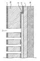
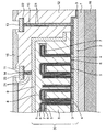
- FIG. 1 is a perspective view illustrating a configuration of a capacitor device according to a first embodiment.
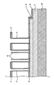
- FIG. 2 is a diagram showing a part of a longitudinal section taken along line A1-A1 ′ of the capacitor device of FIG.
- FIG. 3 is a circuit diagram showing an equivalent circuit of the capacitor device of FIG. 2. It is sectional drawing which shows the 1st state in the manufacturing process of the capacitor apparatus of FIG.
- FIG. 8 is a cross-sectional view showing a second state in the manufacturing process of the capacitor device of FIG. 1.
- FIG. 8 is a cross-sectional view showing a third state in the manufacturing process of the capacitor device of FIG. 1.
- FIG. 7 is a cross-sectional view showing a fourth state in the manufacturing process of the capacitor device of FIG. 1.
- FIG. 1 is a perspective view illustrating a configuration of a capacitor device according to a first embodiment.
- FIG. 2 is a diagram showing a part of a longitudinal section taken along line A1-A1 ′ of the capacitor device
- FIG. 10 is a cross-sectional view showing a fifth state in the manufacturing process of the capacitor device of FIG. 1.
- FIG. 10 is a cross-sectional view showing a sixth state in the manufacturing process of the capacitor device of FIG. 1. It is sectional drawing which shows the 7th state in the manufacturing process of the capacitor apparatus of FIG. It is sectional drawing which shows the 8th state in the manufacturing process of the capacitor apparatus of FIG. It is sectional drawing which shows the 9th state in the manufacturing process of the capacitor apparatus of FIG. It is sectional drawing which shows the 10th state in the manufacturing process of the capacitor apparatus of FIG. It is a perspective view which shows the structure of the capacitor apparatus which concerns on 2nd Embodiment.
- FIG. 10 is a cross-sectional view showing a fifth state in the manufacturing process of the capacitor device of FIG. 1.
- FIG. 10 is a cross-sectional view showing a sixth state in the manufacturing process of the capacitor device of FIG. 1. It is sectional drawing which shows the 7th state in the manufacturing process of the capacitor apparatus of FIG. It is
- FIG. 15 is a view showing a part of a longitudinal section taken along line A2-A2 ′ of the capacitor device of FIG. 14;
- FIG. 15 is a diagram illustrating a part of a longitudinal section taken along line A3-A3 ′ of the capacitor device of FIG. 14.
- FIG. 17 is a circuit diagram showing an equivalent circuit of the capacitor device of FIGS. 15 and 16. It is a capacitor apparatus which concerns on 3rd Embodiment, Comprising: It is a top view which shows the state which has not formed the external terminal.
- FIG. 19 is a top view showing a capacitor device according to a third embodiment in a state in which external terminals 105 and 106 are formed in the capacitor device of FIG. 18. It is a circuit diagram which shows the equivalent circuit of the capacitor apparatus of FIG.
- FIG. 26 is a circuit diagram showing an equivalent circuit of the capacitor device of FIG. 25. It is a top view which shows the structure of the capacitor apparatus which concerns on 6th Embodiment. It is a circuit diagram which shows the equivalent circuit of the capacitor apparatus of FIG.
- FIG. 10 is a schematic diagram for explaining a method for manufacturing a capacitor device according to third to eleventh embodiments.
- FIG. 10 is a schematic diagram for explaining a method for manufacturing a capacitor device according to third to eleventh embodiments.
- FIG. 1 is a perspective view showing the configuration of the capacitor device according to the first embodiment.
- the capacitor device of FIG. 1 includes a capacitor cell 30 formed on a semiconductor substrate having a first surface and a second surface.
- the lower surface of the capacitor device is a first surface
- the upper surface of the capacitor device is a second surface.
- the capacitor cell 30 includes a first electrode including the metal film 2, a second electrode including the metal film 9, and an insulating film (not shown in FIG. 1) formed between the first and second electrodes. ).
- the first electrode including the metal film 2 is also referred to as a lower electrode
- the second electrode including the metal film 9 is also referred to as an upper electrode.
- the capacitor device is electrically connected to the lower electrode including the metal film 2 and electrically connected to at least one first cell terminal including the pad conductor 13 exposed on the upper surface of FIG. 1 and the upper electrode including the metal film 9. And at least one second cell terminal including a pad conductor 14 exposed on the upper surface of FIG.
- the capacitor device includes a plurality of first cell terminals each including a pad conductor 13 and a plurality of second cell terminals each including a pad conductor 14.
- FIG. 2 is a view showing a part of a longitudinal section taken along the line A1-A1 'of the capacitor device of FIG.
- the capacitor device includes an oxide film 1 exposed on the lower surface.
- the oxide film 1 is also referred to as a first silicon oxide film.
- the capacitor device is formed on the oxide film 1 and formed between a lower electrode including a plurality of stacked conductor films, an upper electrode including a plurality of stacked conductor films, and the lower electrode and the upper electrode.
- the insulating film 5 is provided.
- the lower electrode includes a metal film 2 made of tungsten and a conductor film 4 made of Ti—TiN as conductor films.
- the metal film 2 and the conductor film 4 are electrically connected to each other and function as an integrated lower electrode.
- the conductor film 4 functions as a barrier metal.
- the lower electrode further includes a nitride film 3.
- the upper electrode includes a conductor film 6 made of Ti—TiN, doped silicon 8 and a metal film 9 made of tungsten as conductor films.
- the doped silicon 8 fills the hollow space of the crown type stack capacitor with good coverage and improves its mechanical strength.
- the conductor film 6, the doped silicon 8, and the metal film 9 are electrically connected to each other and function as an integral upper electrode.
- the upper electrode further includes a nitride film 7.
- the insulating film 5 is made of, for example, a high dielectric material.
- the insulating film 5 includes, for example, one or more of Ta 2 O 5 material, Al 2 O 3 material, HfO 2 material, ZrO 2 material, and TiO 2 material as a high dielectric material. .
- the lower electrode, the upper electrode, and the insulating film 5 form a capacitor cell 30. Since each of the lower electrode and the upper electrode includes at least one metal film 2 and 9, the capacitor cell 30 is formed as an MIM (Metal-Insulator-Metal) capacitor.
- the capacitor cell 30 is formed as a crown type stack capacitor as shown in FIG.
- the capacitor device includes an interlayer oxide film 12 formed on the metal film 9 of the upper electrode.
- the interlayer oxide film 12 is also referred to as a second silicon oxide film.
- the capacitor device includes a passivation film 15 formed on the interlayer oxide film 12 and exposed on the upper surface.
- the passivation film 15 functions as a protective film that protects the upper surface of the capacitor device.
- the capacitor device is electrically connected to the metal film 2 of the lower electrode and is at least one first cell terminal exposed on the upper surface and electrically connected to the metal film 9 of the upper electrode and exposed at least on the upper surface.
- Each first cell terminal includes a pad conductor 13 exposed on the upper surface and a via conductor 10 electrically connected from the pad conductor 13 to the metal film 2 of the lower electrode.
- the pad conductor 13 is also referred to as a first pad conductor
- the via conductor 10 is also referred to as a first via conductor.
- Each second cell terminal includes a pad conductor 14 exposed on the upper surface and a via conductor 11 electrically connected from the pad conductor 14 to the metal film 9 of the upper electrode.
- the pad conductor 14 is also referred to as a second pad conductor
- the via conductor 11 is also referred to as a second via conductor.
- a barrier metal 21 is formed around the via conductors 10 and 11, and a barrier metal 22 is formed on the lower surfaces of the pad conductors 13 and 14.
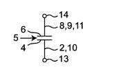
- FIG. 3 is a circuit diagram showing an equivalent circuit of the capacitor device of FIG.
- the conductor films 4 and 6 are capacitively coupled to each other through the insulating film 5.
- the conductor film 4 is electrically connected to the pad conductor 13 through the metal film 2 and the via conductor 10.
- the conductor film 6 is electrically connected to the pad conductor 14 via the doped silicon 8, the metal film 9, and the via conductor 11. Thereby, the capacitor device functions as a capacitor.
- FIG. 4 is a cross-sectional view showing a first state in the manufacturing process of the capacitor device of FIG. FIG. 4 shows a state in which the oxide film 1 and the metal film 2 are formed on the silicon substrate 16 and patterned with a resist mask (not shown).
- a conventional method can be used.
- a thermal oxide film having a high film density may be used as a material that can withstand the mechanical strength at the time of back surface polishing described later.
- FIG. 5 is a cross-sectional view showing a second state in the manufacturing process of the capacitor device of FIG.
- FIG. 5 shows a state where the nitride film 3, another oxide film 1A, and the nitride film 7 are formed after the oxide film 1 and the metal film 2 are formed.
- Prior art methods can be used to form nitride film 3, another oxide film 1A, and nitride film 7.
- the nitride film 7 is formed in order to prevent the crown-type stacked capacitor electrode from falling down in a later step.
- FIG. 6 is a cross-sectional view showing a third state in the manufacturing process of the capacitor device of FIG.
- FIG. 6 shows a state in which the nitride film 7, the oxide film 1A, and the nitride film 3 are patterned and etched to form an opening 17 for the stack capacitor.
- Prior art methods can be used to pattern and etch the nitride film 7, the oxide film 1A, and the nitride film 3.
- FIG. 7 is a cross-sectional view showing a fourth state in the manufacturing process of the capacitor device of FIG.
- FIG. 7 shows a state in which the conductor film 4 is formed and the oxide film 18 is further formed.
- Prior art methods can be used to form the conductor film 4 and the oxide film 18.
- FIG. 8 is a cross-sectional view showing a fifth state in the manufacturing process of the capacitor device of FIG. FIG. 8 shows a state in which the opening 20 for forming the crown type stack capacitor is patterned by the photoresist 19.
- FIG. 9 is a sectional view showing a sixth state in the manufacturing process of the capacitor device of FIG.
- FIG. 9 shows a state in which the photoresist 19 is removed after the oxide film 18 in the opening 20 is etched. Thereafter, the conductor film 4 and the nitride film 7 in the opening 20 are etched using the oxide film 18 as a mask (not shown). At this time, the oxide film 18 and the conductor film 4 serving as a mask are also removed in a self-aligned manner, and a remaining structure of the conductor film 4 forms a crown-shaped structure. Even if the conductor film 4 that becomes a mask remains after etching, it can be removed by performing additional etching only on the conductor film 4.
- FIG. 10 is a cross-sectional view showing a seventh state in the manufacturing process of the capacitor device of FIG.
- FIG. 10 shows a state in which the oxide film 1A remaining immediately under the side wall of the conductor film 4 and the nitride film 7 is removed from the opening formed at the position of the opening 20 in FIG. 9 by a wet process.
- a lower electrode including the metal film 2 and the conductor film 4 as a plurality of stacked conductor films is formed on the oxide film 1.
- FIG. 11 is a sectional view showing an eighth state in the manufacturing process of the capacitor device of FIG.
- the insulating film 5 is formed on the conductor film 4, and the conductor film 6, the doped silicon 8, and the metal film 9 are sequentially formed on the insulating film 5, and then the insulating film 5, the doped silicon is formed. 8 and the metal film 9 are patterned by etching.
- a conventional method can be used in order to pattern the insulating film 5, the doped silicon 8, and the metal film 9 by etching.
- the insulating film 5 is formed on the lower electrode, and the upper electrode including the conductive film 6, the doped silicon 8, and the metal film 9 is formed on the insulating film 5 as a plurality of stacked conductive films. Is done.
- FIG. 12 is a cross-sectional view showing a ninth state in the manufacturing process of the capacitor device of FIG.
- FIG. 12 shows a state in which an interlayer oxide film 12 is formed and planarized on the nitride film 3 and the metal film 9 of the upper electrode.
- Prior art methods can be used to form and planarize the interlayer oxide film 12.
- the planarization may be performed using a chemical mechanical polishing technique, may be performed by removing only the oxide film on the convex portion by patterning and etching, or a combination thereof.
- FIG. 13 is a sectional view showing a tenth state in the manufacturing process of the capacitor device of FIG.
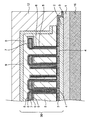
- via conductors 10 and 11 penetrating the interlayer oxide film 12 are formed, pad conductors 13 and 14 are formed on the interlayer oxide film 12, and a passivation film 15 is formed on the interlayer oxide film 12. Shows the state.
- openings are formed only in the portions of the pad conductors 13 and 14.
- Prior art methods can be used to form via conductors 10 and 11.
- the via conductor 10 and the pad conductor 13 are electrically connected to the metal film 2 of the lower electrode and form at least one first cell terminal exposed on the upper surface.
- the via conductor 11 and the pad conductor 14 are electrically connected to the metal film 9 of the upper electrode and form at least one second cell terminal exposed on the upper surface.
- a barrier metal 21 is formed around the via conductors 10 and 11, and a barrier metal 22 is formed on the lower surfaces of the pad conductors 13 and 14.
- the silicon substrate 16 is removed by backside polishing, thereby completing the capacitor device shown in FIG.
- the capacitor device according to the first embodiment does not use a silicon substrate in the capacitor cell 30, the capacitor device operates normally even if the silicon substrate 16 is removed by backside polishing. By removing the silicon substrate 16, the thickness of the capacitor device can be reduced as compared with the conventional case.
- the total thickness of the capacitor device according to the first embodiment can be reduced to about 4 to 5 ⁇ m when configured as a MIM crown type stack capacitor.
- a concave (concavated) stack MIM capacitor according to the prior art may be adopted.
- An advantage of the MIM capacitor is that a desired capacitance can be secured without increasing the thickness of the capacitor device due to the effect of the high dielectric constant of the insulating film.
- a capacitor can be formed without using a structure formed below the surface of a silicon substrate like a trench capacitor, and is very suitable for thinning the capacitor device itself. ing. Furthermore, process development costs can be reduced by diverting general-purpose DRAM semiconductor process technology.
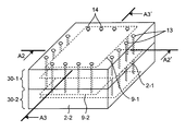
- FIG. 14 is a perspective view showing the configuration of the capacitor device according to the second embodiment.
- the capacitor device of FIG. 14 is configured similarly to the capacitor cell 30 of the capacitor device according to the first embodiment, and a plurality of capacitor cells 30-1 stacked in a direction perpendicular to the lower surface and the upper surface of the semiconductor substrate.
- At least one first cell terminal including the pad conductor 13 is electrically connected to the lower electrode including the metal film 2-1 in the capacitor cell 30-1, and further, the metal film 2-in the capacitor cell 30-2. 2 is electrically connected to the lower electrode.
- At least one second cell terminal including the pad conductor 14 is electrically connected to the upper electrode including the metal film 9-1 in the capacitor cell 30-1, and further, the metal film 9-2 in the capacitor cell 30-2. Is electrically connected to the upper electrode including
- FIG. 15 is a view showing a part of a longitudinal section taken along line A2-A2 'of the capacitor device of FIG.
- FIG. 16 is a view showing a part of a longitudinal section taken along line A3-A3 'of the capacitor device of FIG.
- the capacitor device of FIG. 14 forms the capacitor cell 30 in FIG. 11, forms the interlayer oxide film 12 in FIG. 12 and planarizes the upper surface, and then repeats the steps described with reference to FIGS. Repeatedly, another capacitor cell 30 is formed.
- a plurality of capacitor cells 30-1 and 30-2 are formed that are stacked in a direction perpendicular to the lower surface and the upper surface of the semiconductor substrate.
- the silicon substrate 16 is removed by backside polishing.
- the via conductor 10 is electrically connected to the metal film 2-1 of the lower electrode in the capacitor cell 30-1, and further electrically connected to the metal film 2-2 of the lower electrode in the capacitor cell 30-2. It is formed to be connected. Accordingly, the first cell terminal including the via conductor 10 and the pad conductor 13 is connected to the lower electrodes of the plurality of capacitor cells 30-1 and 30-2. Via conductor 11 is electrically connected to metal film 9-1 of the upper electrode in capacitor cell 30-1, and is further electrically connected to metal film 9-2 of the upper electrode in capacitor cell 30-2. Formed. Accordingly, the second cell terminal including the via conductor 11 and the pad conductor 14 is connected to the upper electrodes of the plurality of capacitor cells 30-1 and 30-2.
- FIG. 17 is a circuit diagram showing an equivalent circuit of the capacitor device of FIGS. 15 and 16.
- the conductor films 4-1 and 6-1 are capacitively coupled to each other through the insulating film 5-1.
- the conductor film 4-1 is electrically connected to the pad conductor 13 through the metal film 2-1 and the via conductor 10.
- the conductor film 6-1 is electrically connected to the pad conductor 14 via doped silicon (not shown), the metal film 9-1, and the via conductor 11.
- the conductor films 4-2 and 6-2 are capacitively coupled to each other through the insulating film 5-2.
- the conductor film 4-2 is electrically connected to the pad conductor 13 through the metal film 2-2 and the via conductor 10.
- the conductor film 6-2 is electrically connected to the pad conductor 14 via doped silicon (not shown), the metal film 9-2, and the via conductor 11.
- the capacitor cells 30-1 and 30-2 are connected in parallel between the pad conductors 13 and 14.
- the capacitor cells 30-1 and 30-2 are stacked and connected in parallel, so that the area of the capacitor cell in the horizontal direction is not increased.
- the capacity can be doubled.
- the via conductors 10 and 11 may be formed using, for example, a conventional TSV (Through Si Via) technique.
- the thickness of the capacitor device can be reduced as compared with the conventional case by removing the silicon substrate, similarly to the capacitor device according to the first embodiment.
- the total thickness of the capacitor device according to the second embodiment is only about 6 to 7 ⁇ m when configured as a MIM crown type stack capacitor.
- the capacitor device according to the second embodiment also has other advantages similar to those of the capacitor device according to the first embodiment.
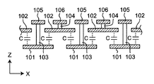
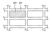
- FIG. 18 is a top view showing the capacitor device according to the third embodiment, in which no external terminal is formed.
- the capacitor device of FIG. 18 includes a plurality of capacitor cells C formed on a rectangular semiconductor substrate having sides extending along a first direction and a second direction orthogonal to each other.
- Each lower electrode 101, each upper electrode 102, each cell terminal 103, and each cell terminal 104 are the lower electrode, the upper electrode, the first cell terminal, and the second electrode of the capacitor device according to the first embodiment. It corresponds to each cell terminal.
- Each lower electrode 101, each upper electrode 102, each cell terminal 103, and each cell terminal 104 are formed on a semiconductor substrate including an oxide film, as in the capacitor device according to the first embodiment. After 18, the semiconductor substrate is omitted for simplification of illustration.
- each lower electrode 101, each upper electrode 102, each cell terminal 103, and each cell terminal 104 is referred to as a first electrode, a second electrode, a first cell terminal, and a second cell terminal. Also called a cell terminal.
- the plurality of lower electrodes 101 includes a portion (for example, a portion corresponding to the metal film 2 in FIG. 2) formed in the first layer of the semiconductor substrate, and is disposed at the first period d1 in the X direction. Arranged in the direction with a second period d2.
- the plurality of upper electrodes 102 include a portion (for example, a portion corresponding to the metal film 9 in FIG. 2) formed in a second layer different from the first layer of the semiconductor substrate, and is arranged with a period d1 in the X direction. And arranged with a period d2 in the Y direction.
- Each upper electrode 102 is arranged so as to be shifted from the lower electrode 101 by a half of the length of the period d1 in the X direction, and is shifted by a half of the length of the period d2 in the Y direction.
- Each lower electrode 101 and each upper electrode 102 are partly opposed and capacitively coupled to each other, and each pair of lower electrode 101 and upper electrode 102 that are capacitively coupled to each other form a capacitor cell C. To do.
- the plurality of cell terminals 103 includes a portion formed in a third layer different from the first and second layers of the semiconductor substrate, and is arranged with a period d1 in the X direction and with a period d2 in the Y direction.
- the plurality of lower electrodes 101 are electrically connected to each other.
- the second layer is located between the first and third layers.
- the plurality of cell terminals 104 include a portion formed in the third layer of the semiconductor substrate, and are arranged with a period d1 in the X direction and with a period d2 in the Y direction, and are electrically connected to the plurality of upper electrodes 102, respectively. Connected.
- Each cell terminal 104 is arranged so as to be shifted from the cell terminal 103 by half the length of the period d1 in the X direction, and is shifted by half the length of the period d2 in the Y direction.
- the capacitor device includes two lower electrodes 101 adjacent to each other in the Y direction and two upper electrodes 102 adjacent to each other in the X direction (or two lower electrodes 101 adjacent to each other in the X direction; A plurality of unit cells 100 (including two upper electrodes 102 adjacent to each other in the Y direction) are included.
- Each unit cell 100 includes four capacitor cells C formed from a pair of lower electrode 101 and upper electrode 102 that are capacitively coupled to face each other. Capacitor cells C having a desired number of rows and columns are formed by repeatedly arranging a plurality of unit cells 100.
- the capacitor device according to the third embodiment may be configured similarly to the capacitor device according to the first embodiment.
- the semiconductor substrate has a first surface and a second surface.
- the capacitor device includes a first silicon oxide film exposed on the first surface and a passivation film exposed on the second surface.
- Each lower electrode 101 is formed on the first silicon oxide film and includes a plurality of stacked conductor films.
- Each upper electrode 102 includes a plurality of stacked conductor films.
- the capacitor device further includes an insulating film formed between each lower electrode 101 and each upper electrode 102 and a second silicon oxide film formed on each upper electrode 102.
- the passivation film is formed on the second silicon oxide film.
- Cell terminals 103 and 104 are exposed on the second surface.
- Each capacitor cell C is formed of a pair of lower electrode 101 and upper electrode 102 that are capacitively coupled to face each other, and an insulating film formed therebetween.
- Each capacitor cell C may be formed as a crown type stack capacitor.
- the cell terminals 103 and 104 may be configured in the same manner as the first and second cell terminals of the capacitor device according to the first embodiment.
- each cell terminal 103 is electrically connected to the first pad conductor formed on the third layer of the semiconductor substrate and one of the plurality of lower electrodes 101 from the first pad conductor. And a first via conductor.
- each cell terminal 104 is electrically connected to a second pad conductor formed on the third layer of the semiconductor substrate and one of the plurality of upper electrodes 102 from the second pad conductor. A second via conductor.
- FIG. 19 is a top view showing the capacitor device according to the third embodiment, in which the external terminals 105 and 106 are formed on the capacitor device of FIG.
- the capacitor device further includes at least two external terminals 105 and 106 for electrical connection to a circuit external to the capacitor device.
- Each external terminal 105 and 106 is electrically connected to a part of the plurality of cell terminals including the plurality of cell terminals 103 and the plurality of cell terminals 104, respectively.
- the plurality of cell terminals 103 and 104 respectively extend in the Y direction and form a plurality of cell terminal rows adjacent to each other in the extending direction.
- the capacitor device includes external terminals 105 and 106 each having a comb shape.
- the external terminal 105 includes a plurality of first portions (portions extending in the Y direction) electrically connected to every 2N cell terminal rows of the plurality of cell terminal rows when N is an integer. And a second portion (a portion extending in the X direction) that connects the first portions to each other.
- the external terminal 106 also includes a plurality of first portions (portions extending in the Y direction) electrically connected to every 2N cell terminal rows of the plurality of cell terminal rows, and a first portion. And a second portion (a portion extending in the X direction) connected to each other.
- Each first portion of the external terminal 105 and each first portion of the external terminal 106 are formed so as to be fitted to each other.
- Each of the external terminals 105 and 106 is arranged such that every N cell terminal rows of the plurality of cell terminal rows are electrically connected to the external terminals 105 and 106 alternately.
- External terminals 105 and 106 can be connected to a voltage source having an arbitrary voltage.
- a voltage source having an arbitrary voltage.
- one of them may be connected to a power source and the other may be grounded.
- the external terminals 105 and 106 are electrically connected to a circuit external to the capacitor device at a portion electrically connected to one of the plurality of cell terminal rows (that is, each first portion of the external terminals 105 and 106). May be connected. Instead, the external terminals 105 and 106 may be electrically connected to a circuit outside the capacitor device in their respective second portions (portions extending in the X direction).
- FIG. 20 is a circuit diagram showing an equivalent circuit of the capacitor device of FIG. As described above, each capacitor cell C is formed between each pair of the lower electrode 101 and the upper electrode 102 that are capacitively coupled to face each other. According to FIG. 20, one capacitor cell C is formed between the external terminals 105 and 106 adjacent to each other. Therefore, in the entire capacitor device, a plurality of capacitor cells C are connected in parallel.
- FIG. 21 is a schematic diagram showing a current flowing through the capacitor device of FIG.
- the external terminals 105 and 106 are omitted.
- the equivalent series inductance ESL
- the equivalent series inductance can be reduced by arranging each lower electrode 101, each upper electrode 102, each cell terminal 103, and each cell terminal 104 periodically and symmetrically.
- the equivalent series inductance is best reduced when a fine pitch bump is formed in a portion where the external terminals 105 and 106 are electrically connected to one of the plurality of cell terminal rows. .
- the period d1 in which each lower electrode 101, each upper electrode 102, each cell terminal 103, and each cell terminal 104 are arranged in the X direction and the period d2 in which each cell terminal 104 is arranged in the Y direction may be set to be equal to each other. May be set.
- FIG. 22 is a top view showing a part of the capacitor device according to the modification of the third embodiment and showing a state in which no external terminal is formed.
- the period d1 'for arranging each upper electrode 102, each cell terminal 103, and each cell terminal 104 in the X direction and the period d2' for arranging in the Y direction are set to be different from each other.
- the unit cell 100A includes two lower electrodes 101 adjacent in the Y direction and two upper electrodes 102 adjacent in the X direction.
- the capacitor device of FIG. 22 can also operate in the same manner as the capacitor device of FIG.
- a capacitor device having characteristics such as a different capacitance, a different capacitance density, a different breakdown voltage, and / or a different position and number of terminals from the capacitor device of FIG.
- a mask for forming the external terminals 105 and 106 may be replaced as described in the following embodiments.
- a plurality of expensive masks are required.
- the capacitor device according to the third embodiment when customizing the capacitor device according to customer requirements, by changing only one (or a small number) of relatively inexpensive masks, the external terminals 105 and 106 can be changed. The shape can be changed, whereby the characteristics of the capacitor described above can be changed. At this time, it is not necessary to change the mask for forming the plurality of capacitor cells C.
- FIG. 23 is a top view showing the configuration of the capacitor device according to the fourth embodiment.
- the capacitor device of FIG. 23 includes external terminals 105A and 106A each having a comb shape.
- the external terminals 105A extend in the Y direction and are electrically connected to every four cell terminal rows of the plurality of adjacent cell terminal rows, and the external terminal 106A is also a plurality of cell terminals. It is electrically connected to every four cell terminal rows in the row.
- Each of the external terminals 105A and 106A is arranged such that every two cell terminal rows of the plurality of cell terminal rows are electrically connected to the external terminals 105A and 106A alternately.
- the capacitor device of FIG. 23 further includes a plurality of floating terminals 107 that are respectively electrically connected to the cell terminal row including the cell terminals 103 that are not connected to the external terminals 105A and 106A due to the convenience of the semiconductor process technology. Each floating terminal 107 is not connected to other circuits.
- FIG. 24 is a circuit diagram showing an equivalent circuit of the capacitor device of FIG. According to FIG. 24, two capacitor cells C are formed between the external terminals 105A and 106A adjacent to each other. Therefore, in the entire capacitor device, a plurality of circuits each including two capacitor cells C connected in series are connected in parallel.
- FIG. 25 is a top view showing the configuration of the capacitor device according to the fifth embodiment.
- the capacitor device of FIG. 25 includes external terminals 105B and 106B each having a comb shape.
- the external terminals 105B extend in the Y direction and are electrically connected to every six cell terminal rows among the plurality of adjacent cell terminal rows, and the external terminal 106B also has a plurality of cell terminals. It is electrically connected to every six cell terminal rows in the row.
- Each of the external terminals 105B and 106B is arranged such that every three cell terminal rows of the plurality of cell terminal rows are electrically connected to the external terminals 105B and 106B alternately.
- the capacitor device of FIG. 25 further includes a plurality of floating terminals 107 and 108 that are electrically connected to cell terminal rows that are not connected to the external terminals 105B and 106B, respectively, for the convenience of semiconductor process technology.
- Each floating terminal 107 is electrically connected to a cell terminal row including cell terminals 103
- each floating terminal 108 is electrically connected to a cell terminal row including cell terminals 104.
- Each floating terminal 107 and 108 is not connected to other circuits.
- FIG. 26 is a circuit diagram showing an equivalent circuit of the capacitor device of FIG. According to FIG. 26, three capacitor cells C are formed between the external terminals 105B and 106B adjacent to each other. Therefore, in the entire capacitor device, a plurality of circuits each including three capacitor cells C connected in series are connected in parallel.
- FIG. 27 is a top view showing the configuration of the capacitor device according to the sixth embodiment.
- the capacitor device of FIG. 27 includes external terminals 105C and 106C each having a comb shape.
- Each of the external terminals 105C and 106C is arranged such that every four cell terminal rows of the plurality of cell terminal rows are electrically connected to the external terminals 105C and 106C alternately.
- the capacitor device of FIG. 27 further includes a plurality of floating terminals 107 and 108 that are electrically connected to cell terminal rows that are not connected to the external terminals 105C and 106C, respectively, due to the convenience of semiconductor process technology.
- Each floating terminal 107 is electrically connected to a cell terminal row including cell terminals 103
- each floating terminal 108 is electrically connected to a cell terminal row including cell terminals 104.
- Each floating terminal 107 and 108 is not connected to other circuits.
- FIG. 28 is a circuit diagram showing an equivalent circuit of the capacitor device of FIG. According to FIG. 28, four capacitor cells C are formed between the external terminals 105C and 106C adjacent to each other. Therefore, in the entire capacitor device, a plurality of circuits each including four capacitor cells C connected in series are connected in parallel.
- a pair of external terminals includes a pair of cell terminal rows every N of the plurality of cell terminal rows. You may arrange
- the number of capacitor cells C connected in series can be changed by changing the shape of the external terminal.
- the number of capacitor cells C connected in series is inversely proportional to the capacity density and breakdown voltage of the capacitor device.
- FIG. 29 is a top view showing the configuration of the capacitor device according to the seventh embodiment.
- the plurality of external terminals 105 and 106 are not limited to being formed in the same layer.
- the external terminal 105 is formed below the lower electrode 101, and the external terminal 106 is formed above the upper electrode 102.
- the capacitor device according to the seventh embodiment can also operate in the same manner as the capacitor device according to the third embodiment.
- FIG. 30 is a top view showing the configuration of the capacitor device according to the eighth embodiment.
- the plurality of cell terminals 103 and 104 extend in the X direction and are adjacent to each other in the extending direction instead of the cell terminal rows extending in the Y direction as in the third to seventh embodiments.
- the cell terminal array may be formed.
- the capacitor device includes external terminals 105D and 106D each having a comb shape.
- the external terminal 105D has a plurality of first portions (portions extending in the X direction) electrically connected to every 2N cell terminal rows of the plurality of cell terminal rows when N is an integer. , And a second portion (a portion extending in the Y direction) that connects the first portions to each other.
- the external terminal 106D also includes a plurality of first portions (portions extending in the X direction) electrically connected to every 2N cell terminal rows of the plurality of cell terminal rows, and a first portion. And a second portion (a portion extending in the Y direction) connected to each other.
- Each first portion of the external terminal 105D and each first portion of the external terminal 106D are formed so as to be fitted to each other.
- Each of the external terminals 105D and 106D is arranged such that every N cell terminal rows of the plurality of cell terminal rows are electrically connected to the external terminals 105D and 106D alternately.
- the external terminals 105D and 106D are electrically connected to a circuit outside the capacitor device in a portion electrically connected to one of the plurality of cell terminal rows (that is, each first portion of the external terminals 105D and 106D). May be connected. Instead, the external terminals 105D and 106D may be electrically connected to a circuit outside the capacitor device in their respective second portions (portions extending in the Y direction).
- a pair of external terminals includes a pair of cell terminal rows every N of the plurality of cell terminal rows. You may arrange
- the capacitor device may include external terminals 105D and 106D formed as in the eighth embodiment, and these external terminals 105D and 106D are short sides (sides extending in the Y direction) of the rectangular capacitor device. ) May be electrically connected to a circuit outside the capacitor device.
- the capacitor device may include external terminals 105 and 106 formed as in the third to seventh embodiments, and these external terminals 105 and 106 are the length of the rectangular capacitor device. The side (side extending in the X direction) may be electrically connected to a circuit outside the capacitor device.
- the equivalent series inductance is higher in the third to seventh embodiments than in the case where the short side of the rectangular capacitor device is electrically connected to a circuit outside the capacitor device as in the eighth embodiment.
- the case where the long side of the rectangular capacitor device is electrically connected to a circuit outside the capacitor device is reduced.
- FIG. 31 is a top view showing the configuration of the capacitor device according to the ninth embodiment.
- the plurality of cell terminals 103 and 104 respectively extend in the Y direction and form a plurality of cell terminal rows adjacent to each other in the extending direction.
- the capacitor device includes external terminals 111 and 112 each having a comb shape, and an external terminal 113 having a fishbone shape.
- the external terminal 113 includes a plurality of first portions (portions extending in the Y direction) electrically connected to every 2N cell terminal rows of the plurality of cell terminal rows when N is an integer. And a second portion (a portion extending in the X direction) for connecting the first portions of the external terminals 113 to each other at the center of the first portions of the external terminals 113.
- the external terminal 111 includes a plurality of first portions (extending in the Y direction) that are electrically connected to a part of the plurality of cell terminals included in every 2N cell terminal rows of the plurality of cell terminal rows.
- the external terminal 111 is formed on the first side with respect to the second portion of the external terminal 113 so as to be fitted to the first portion of the external terminal 113.
- the external terminal 112 includes a plurality of first portions (extending in the Y direction) that are electrically connected to a part of the plurality of cell terminals included in every 2N cell terminal rows of the plurality of cell terminal rows. And a second portion (a portion extending in the X direction) that connects the first portions of the external terminals 112 to each other.
- the external terminal 112 is formed to be fitted to the first portion of the external terminal 113 on the second side opposite to the first side with respect to the second portion of the external terminal 113.
- Each of the external terminals 111 to 113 is arranged such that every N cell terminal rows of the plurality of cell terminal rows are electrically connected to the external terminals 111 and 112 and the external terminal 113 alternately.
- the external terminal 111 is electrically connected to a part of the plurality of cell terminals included in every two cell terminal rows of the plurality of cell terminal rows.
- Each of the external terminals 112 to 113 electrically connected to a part of the plurality of cell terminals included in every two cell terminal columns of the plurality of cell terminal columns
- the cell terminal rows are arranged so as to be electrically connected to the external terminals 111 and 112 and the external terminal 113 alternately.
- External terminals 111 and 112 may be electrically connected to a circuit outside the capacitor device on the long side (side extending in the X direction) of the capacitor device.
- the external terminal 113 may be electrically connected to a circuit outside the capacitor device on the short side (side extending in the Y direction) of the capacitor device.
- the external terminal 113 is connected to a power source, for example, and the external terminals 111 and 112 are grounded, for example.
- the capacitor device according to the ninth embodiment has an effect of reducing the equivalent series inductance compared to the third to eighth embodiments by changing the shape of the external terminal.
- FIG. 32 is a top view showing the configuration of the capacitor device according to the tenth embodiment.
- the plurality of cell terminals 103 and 104 respectively extend in the Y direction and form a plurality of cell terminal rows adjacent to each other in the extending direction.
- the capacitor device includes external terminals 111A and 112A each having a comb shape, and an external terminal 113A having a meander shape.
- the external terminal 113A has a plurality of first portions (portions extending in the Y direction) electrically connected to every 2N cell terminal rows of the plurality of cell terminal rows when N is an integer.
- the external terminal 111A includes a plurality of first portions (portions extending in the Y direction) electrically connected to every 4N cell terminal rows of the plurality of cell terminal rows, and each of the external terminals 111A. And a second portion (a portion extending in the X direction) that connects the first portions to each other.
- the external terminal 111A is formed on the first side with respect to the external terminal 113A so as to be fitted to the first portion of the external terminal 113A.
- the external terminal 112A includes a plurality of first portions (portions extending in the Y direction) electrically connected to every 4N cell terminal rows of the plurality of cell terminal rows, and each of the external terminals 112A.
- the external terminal 112A is formed to be fitted to the first portion of the external terminal 113A on the second side opposite to the first side with respect to the external terminal 113A.
- Each of the external terminals 111A to 113A is arranged such that every N cell terminal rows of the plurality of cell terminal rows are electrically connected to the external terminals 111A or 112A and the external terminals 113A alternately.
- the external terminal 111A is electrically connected to every four cell terminal rows of the plurality of cell terminal rows.
- the external terminal 112A is electrically connected to every four cell terminal rows of the plurality of cell terminal rows.
- Each of the external terminals 111A to 113A is arranged such that a plurality of cell terminal arrays are alternately electrically connected to the external terminals 111A or 112A and the external terminals 113A.
- External terminals 111A and 112A may be electrically connected to a circuit outside the capacitor device on the long side (side extending in the X direction) of the capacitor device.
- the external terminal 113A may be electrically connected to a circuit outside the capacitor device on the short side (side extending in the Y direction) of the capacitor device.
- the external terminal 113A is connected to a power source, for example, and the external terminals 111A and 112A are grounded, for example.
- the capacitor device of the tenth embodiment by changing the shape of the external terminal, it is equivalent to the third to eighth embodiments as in the case of the ninth embodiment. There is an effect of reducing the series inductance.
- FIG. 33 is a top view showing the configuration of the capacitor device according to the eleventh embodiment.
- the capacitor device may include four or more external terminals.
- the plurality of cell terminals 103 and 104 respectively extend in the Y direction and form a plurality of cell terminal rows adjacent to each other in the extending direction.
- the capacitor device includes a plurality of sets of external terminals each including first and second external terminals.
- a set including the external terminals 121 and 125, a set including the external terminals 122 and 126, a set including the external terminals 123 and 126, and a set including the external terminals 124 and 127 are provided.
- Each of the first and second external terminals of each set includes a portion that is electrically connected to at least one cell terminal row of the plurality of cell terminal rows.
- Each of the first and second external terminals of each set is such that when N is an integer, every N cell terminal rows of the plurality of cell terminal rows are alternately connected to the first and second external terminals. Arranged to be connected to each other.
- the external terminals 125 to 127 are connected to a power source, for example, and the external terminals 121 to 124 are grounded, for example.
- a plurality of cell terminal arrays are alternately electrically connected to the external terminals 125 to 127 connected to the power source and the grounded external terminals 121 to 124. Placed in. Further, among the long sides (sides extending in the X direction) of the capacitor device, the external terminals 125 and 126 connected to the power source and the external terminals 122 and 124 grounded are alternately provided on the + Y side. .
- the external terminals 126 and 127 connected to the power source and the external terminals 121 and 123 connected to the ground alternately on the ⁇ Y side side.
- the capacitor device according to the eleventh embodiment has an effect of further reducing the equivalent series inductance as compared to the ninth and tenth embodiments by changing the shape of the external terminal.
- the capacitor devices according to the third to eleventh embodiments can be manufactured, for example, by the following manufacturing process.
- the manufacturing method includes a plurality of lower electrodes 101 including a portion formed in a first layer of a semiconductor substrate, arranged at a period d1 in the X direction and arranged at a period d2 in the Y direction.
- a plurality of upper electrodes including a step of forming an electrode 101 and a portion formed in a second layer different from the first layer of the semiconductor substrate, the electrodes being arranged at a period d1 in the X direction, and in the Y direction; Forming a plurality of upper electrodes 102 arranged at a period d2.
- each upper electrode 102 is arranged so as to be shifted by half the length of the period d1 in the X direction with respect to each lower electrode 101 and shifted by half the length of the period d2 in the Y direction. Including placing.
- Each lower electrode 101 and each upper electrode 102 are partly opposed and capacitively coupled to each other, and each pair of lower electrode 101 and upper electrode 102 that are capacitively coupled to each other form a capacitor cell C. To do.
- the manufacturing method includes a plurality of cell terminals 103 including a portion formed in a third layer different from the first and second layers of the semiconductor substrate, arranged at a period d1 in the X direction, and a period in the Y direction. a step of forming a plurality of cell terminals 103 arranged at d2 and electrically connected to the plurality of lower electrodes 101, and a plurality of cell terminals 104 including a portion formed in the third layer of the semiconductor substrate And forming a plurality of cell terminals 104 arranged in the X direction at a period d1 and arranged in the Y direction at a period d2 and electrically connected to the plurality of upper electrodes 102, respectively.
- the second layer is located between the first and third layers.
- each cell terminal 104 is arranged with respect to each cell terminal 103 by being shifted by half the length of the period d1 in the X direction and by being shifted by half the length of the period d2 in the Y direction. Including doing.
- the manufacturing method further includes forming at least two external terminals that are respectively electrically connected to a part of the plurality of cell terminals including the plurality of cell terminals 103 and the plurality of cell terminals 104.
- 34 and 35 are schematic views for explaining the capacitor device manufacturing method according to the third to eleventh embodiments.
- MLCC multilayer ceramic capacitor
- Many of such capacitor devices have a rectangular parallelepiped outer shape and are external terminals having the shapes described in the third to eleventh embodiments, and have been described in the third to eleventh embodiments.
- an external terminal connected to an external circuit is provided.
- Various configurations can be taken by providing compatibility with MLCC when mounting the capacitor device and changing only one mask to meet customer requirements.
- MLCC capacitor devices are available in various sizes.
- a scribe line and a guard ring are arranged so that a chip having the smallest size can be cut out from a silicon wafer.
- the size of the capacitor device can be changed by changing only three masks as described below. Thereafter, by removing the scribe line and the guard ring, it is possible to connect the chips of each capacitor device with metal wiring. For this reason, the size of the capacitor device can be changed to be scalable.
- metal wiring 211 used as a scribe line and a guard ring is formed on a semiconductor substrate in the manufacturing process of the capacitor device.
- the capacitor device region 201 has, for example, a 05025 size (500 ⁇ 250 ⁇ m).
- a metal wiring 212 is formed on the semiconductor substrate.
- the region 202 of the capacitor device having a 1005 size 1000 ⁇ 500 ⁇ m) can be obtained.
- the manufacturing method performs the following steps according to a desired position where the external terminal is electrically connected to a circuit outside the capacitor device, a desired capacitance and desired breakdown voltage of the capacitor device, and a size of the capacitor device. To do. That is, the manufacturing method includes a step of selecting a first mask for forming a metal wiring used as a scribe line and a guard ring, a step of selecting a second mask for forming an external terminal, Selecting a third mask for forming a cell terminal for connecting the metal wiring and the external terminal to each other among the cell terminals.
- the capacitor devices according to the third to eleventh embodiments only a small number of masks need be changed, so that the design change of the capacitor device can be performed at low cost.
- the number of rows and / or columns of the capacitor cell C of the capacitor device is equal to the number of capacitor cells connected in series required for each application. Set to least common multiple or multiple.
- the capacitor device according to each embodiment of the present invention is useful, for example, as an on-package decoupling capacitor.
- semiconductor devices there are problems such as a decrease in voltage tolerance range due to a decrease in power supply voltage, generation of large power supply noise or ground noise due to an increase in current consumption, and a decrease in EMI resistance due to an increase in operating frequency.
- problems such as a decrease in voltage tolerance range due to a decrease in power supply voltage, generation of large power supply noise or ground noise due to an increase in current consumption, and a decrease in EMI resistance due to an increase in operating frequency.
- it is effective to use a decoupling capacitor.
- By using the capacitor device according to each embodiment of the present invention it is possible to provide a semiconductor device in which the above problems are reduced.
Landscapes
- Engineering & Computer Science (AREA)
- Power Engineering (AREA)
- Computer Hardware Design (AREA)
- Microelectronics & Electronic Packaging (AREA)
- Physics & Mathematics (AREA)
- Condensed Matter Physics & Semiconductors (AREA)
- General Physics & Mathematics (AREA)
- Manufacturing & Machinery (AREA)
- Geometry (AREA)
- Semiconductor Integrated Circuits (AREA)
- Ceramic Capacitors (AREA)
- Fixed Capacitors And Capacitor Manufacturing Machines (AREA)
Abstract
各下側電極(101,102)は、X方向に周期d1で配置され、Y方向に周期d2で配置される。各上側電極(102)は、各下側電極(101)に対して、X方向に周期(d1)の長さの半分だけずらして配置され、Y方向に周期(d2)の長さの半分だけずらして配置される。互いに対向して容量的に結合する各一対の下側電極(101)及び上側電極(102)はキャパシタセル(C)を形成する。各セル端子(103,104)は、X方向に周期(d1)で配置され、Y方向に周期(d2)で配置され、各下側電極(101)及び各上側電極(102)にそれぞれ電気的に接続される。各セル端子(104)は、各セル端子(103)に対して、X方向に周期(d1)の長さの半分だけずらして配置され、Y方向に周期(d2)の長さの半分だけずらして配置される。
Description
本発明は、半導体基板上に形成された1つ又は複数のキャパシタセルを含むキャパシタ装置とその製造方法に関する。
半導体プロセス技術を用いて半導体基板上に形成された1つ又は複数のキャパシタセルを含むキャパシタ装置が知られている。このようなキャパシタ装置は、容量の増大、サイズの削減、製造コストの低減、設計変更の容易さなど、さまざまな要件を満たすことが求められる。
特許文献1は、半導体基板の表面に対して垂直方向に形成された構造物を有するトレンチキャパシタを開示している。
キャパシタ装置は、回路のさらなる集積化のために、端子(半田ボールなど)の直径及び間隔を削減するとともに、キャパシタ装置の厚さを削減することが求められる。
特許文献1のようなトレンチキャパシタの場合、トレンチキャパシタはシリコン基板中に形成されるので、製造工程でシリコン基板の表面を研磨する際には、キャパシタ部分を残すように研磨する必要がある。従って、研磨により削減可能なシリコン基板の厚さ(深さ)は制限される。また、半導体プロセス技術の微細化によりトレンチキャパシタの深さは益々増大し、10μmを越える深さを有するトレンチキャパシタも存在する。従って、トレンチキャパシタの深さが増大する分だけ、最終的なキャパシタ装置の厚さも増大する。従って、このような制約を受けることなく、従来よりも削減された厚さを有するキャパシタ装置が求められる。
また、半導体プロセス技術を用いて、異なる容量、異なる容量密度(単位体積あたりの容量)、異なる耐圧、及び/又は、端子の異なる位置及び個数などの特性を有するキャパシタ装置を製造する場合、従来であれば、マスクを作り直す必要があるので、大きなコストがかかっていた。従って、従来よりも低いコストで上述したキャパシタの特性を変更して製造可能なキャパシタ装置が求められる。
本発明の目的は、半導体基板上に形成された1つ又は複数のキャパシタセルを含むキャパシタ装置であって、従来よりも削減された厚さを有するキャパシタ装置を提供することにある。
また、本発明の目的は、半導体基板上に形成された1つ又は複数のキャパシタセルを含むキャパシタ装置であって、従来よりも低いコストで上述したキャパシタの特性を変更して製造可能なキャパシタ装置が求められる。
さらに、本発明の目的は、そのようなキャパシタ装置の製造方法を提供することにある。
本発明の第1の態様に係るキャパシタ装置は、
互いに直交する第1の方向及び第2の方向に沿って延在する辺を有する矩形の半導体基板に形成された複数のキャパシタセルを含むキャパシタ装置であって、
前記キャパシタ装置は、
前記半導体基板の第1の層に形成された部分を含む複数の第1の電極であって、前記第1の方向に第1の周期で配置され、かつ、前記第2の方向に第2の周期で配置された複数の第1の電極と、
前記半導体基板の第1の層とは異なる第2の層に形成された部分を含む複数の第2の電極であって、前記第1の方向に前記第1の周期で配置され、かつ、前記第2の方向に前記第2の周期で配置された複数の第2の電極とを備え、
前記各第2の電極は、前記各第1の電極に対して、前記第1の方向に前記第1の周期の長さの半分だけずらして配置され、かつ、前記第2の方向に前記第2の周期の長さの半分だけずらして配置され、
前記各第1の電極及び前記各第2の電極は互いに部分的に対向して容量的に結合し、互いに対向して容量的に結合する各一対の前記第1及び第2の電極はキャパシタセルを形成し、
前記キャパシタ装置は、
前記半導体基板の第1及び第2の層とは異なる第3の層に形成された部分を含む複数の第1のセル端子であって、前記第1の方向に前記第1の周期で配置され、前記第2の方向に前記第2の周期で配置され、かつ、前記複数の第1の電極にそれぞれ電気的に接続された複数の第1のセル端子と、
前記半導体基板の第3の層に形成された部分を含む複数の第2のセル端子であって、前記第1の方向に前記第1の周期で配置され、前記第2の方向に前記第2の周期で配置され、かつ、前記複数の第2の電極にそれぞれ電気的に接続された複数の第2のセル端子とをさらに備え、
前記第2の層は前記第1及び第3の層の間に位置し、
前記各第2のセル端子は、前記各第1のセル端子に対して、前記第1の方向に前記第1の周期の長さの半分だけずらして配置され、かつ、前記第2の方向に前記第2の周期の長さの半分だけずらして配置される。
本発明の第2の態様に係るキャパシタ装置は、第1の態様に係るキャパシタ装置において、
前記キャパシタ装置は少なくとも2つの外部端子をさらに備え、前記各外部端子は、前記複数の第1のセル端子及び前記複数の第2のセル端子を含む複数のセル端子のうちの一部にそれぞれ電気的に接続される。
前記キャパシタ装置は少なくとも2つの外部端子をさらに備え、前記各外部端子は、前記複数の第1のセル端子及び前記複数の第2のセル端子を含む複数のセル端子のうちの一部にそれぞれ電気的に接続される。
本発明の第3の態様に係るキャパシタ装置は、第2の態様に係るキャパシタ装置において、
前記複数のセル端子は、前記第1の方向又は前記第2の方向にそれぞれ延在し、延在方向に互いに隣接する複数のセル端子列を形成し、
前記キャパシタ装置は、櫛形形状をそれぞれ有する第1及び第2の外部端子を備え、
前記第1及び第2の外部端子のそれぞれは、Nが整数であるとき、前記複数のセル端子列のうちの2N個毎のセル端子列に電気的に接続される複数の第1の部分と、前記第1の部分を互いに接続する第2の部分とを備え、前記第1の外部端子の各第1の部分と前記第2の外部端子の各第1の部分とは互いに嵌合するように形成され、
前記第1及び第2の外部端子は、前記複数のセル端子列のうちのN個毎のセル端子列が前記第1及び第2の外部端子に交互に電気的に接続されるように配置される。
本発明の第4の態様に係るキャパシタ装置は、第2の態様に係るキャパシタ装置において、
前記複数のセル端子は、前記第1の方向又は前記第2の方向にそれぞれ延在し、延在方向に互いに隣接する複数のセル端子列を形成し、
前記キャパシタ装置は、フィッシュボーン形状を有する第1の外部端子と、櫛形形状をそれぞれ有する第2及び第3の外部端子とを備え、
前記第1の外部端子は、Nが整数であるとき、前記複数のセル端子列のうちの2N個毎のセル端子列に電気的に接続される複数の第1の部分と、前記第1の外部端子の各第1の部分の中央において前記第1の外部端子の各第1の部分を互いに接続する第2の部分とを備え、
前記第2の外部端子は、前記複数のセル端子列のうちの2N個毎のセル端子列に含まれる複数のセル端子のうちの一部に電気的に接続される複数の第1の部分と、前記第2の外部端子の各第1の部分を互いに接続する第2の部分とを備え、前記第2の外部端子は、前記第1の外部端子の第2の部分を基準として第1の側において、前記第1の外部端子の第1の部分に対して嵌合するように形成され、
前記第3の外部端子は、前記複数のセル端子列のうちの2N個毎のセル端子列に含まれる複数のセル端子のうちの一部に電気的に接続される複数の第1の部分と、前記第3の外部端子の各第1の部分を互いに接続する第2の部分とを備え、前記第3の外部端子は、前記第1の外部端子の第2の部分を基準として前記第1の側の逆の第2の側において、前記第1の外部端子の第1の部分に対して嵌合するように形成され、
前記第1~第3の外部端子は、前記複数のセル端子列のうちのN個毎のセル端子列が前記第1の外部端子と前記第2又は第3の外部端子とに交互に電気的に接続されるように配置される。
本発明の第5の態様に係るキャパシタ装置は、第2の態様に係るキャパシタ装置において、
前記複数のセル端子は、前記第1の方向又は前記第2の方向にそれぞれ延在し、延在方向に互いに隣接する複数のセル端子列を形成し、
前記キャパシタ装置は、ミアンダ形状を有する第1の外部端子と、櫛形形状をそれぞれ有する第2及び第3の外部端子とを備え、
前記第1の外部端子は、Nが整数であるとき、前記複数のセル端子列のうちの2N個毎のセル端子列に電気的に接続される複数の第1の部分と、前記第1の外部端子の各第1の部分の長手方向の両端のうちのいずれかにおいて前記第1の外部端子の各第1の部分を互いに接続する複数の第2の部分とを備え、
前記第2の外部端子は、前記複数のセル端子列のうちの4N個毎のセル端子列に電気的に接続される複数の第1の部分と、前記第2の外部端子の各第1の部分を互いに接続する第2の部分とを備え、前記第2の外部端子は、前記第1の外部端子を基準として第1の側において、前記第1の外部端子の第1の部分に対して嵌合するように形成され、
前記第3の外部端子は、前記複数のセル端子列のうちの4N個毎のセル端子列に電気的に接続される複数の第1の部分と、前記第3の外部端子の各第1の部分を互いに接続する第2の部分とを備え、前記第3の外部端子は、前記第1の外部端子を基準として前記第1の側の逆の第2の側において、前記第1の外部端子の第1の部分に対して嵌合するように形成され、
前記第1~第3の外部端子は、前記複数のセル端子列のうちのN個毎のセル端子列が前記第1の外部端子と前記第2又は第3の外部端子とに交互に電気的に接続されるように配置される。
本発明の第6の態様に係るキャパシタ装置は、第2の態様に係るキャパシタ装置において、
前記複数のセル端子は、前記第1の方向又は前記第2の方向にそれぞれ延在し、延在方向に互いに隣接する複数のセル端子列を形成し、
前記キャパシタ装置は、第1及び第2の外部端子をそれぞれ含む複数組の外部端子を備え、
前記各組の第1及び第2の外部端子のそれぞれは、前記複数のセル端子列のうちの少なくとも1つのセル端子列に電気的に接続される部分を備え、
前記各組の第1及び第2の外部端子は、Nが整数であるとき、前記複数のセル端子列のうちのN個毎のセル端子列が前記第1及び第2の外部端子に交互に電気的に接続されるように配置される。
前記複数のセル端子は、前記第1の方向又は前記第2の方向にそれぞれ延在し、延在方向に互いに隣接する複数のセル端子列を形成し、
前記キャパシタ装置は、第1及び第2の外部端子をそれぞれ含む複数組の外部端子を備え、
前記各組の第1及び第2の外部端子のそれぞれは、前記複数のセル端子列のうちの少なくとも1つのセル端子列に電気的に接続される部分を備え、
前記各組の第1及び第2の外部端子は、Nが整数であるとき、前記複数のセル端子列のうちのN個毎のセル端子列が前記第1及び第2の外部端子に交互に電気的に接続されるように配置される。
本発明の第7の態様に係るキャパシタ装置は、第3~第6のうちの1つの態様に係るキャパシタ装置において、
前記各外部端子は、前記複数のセル端子列のうちの1つに電気的に接続される部分において、前記キャパシタ装置の外部の回路に電気的に接続される。
前記各外部端子は、前記複数のセル端子列のうちの1つに電気的に接続される部分において、前記キャパシタ装置の外部の回路に電気的に接続される。
本発明の第8の態様に係るキャパシタ装置は、第1~第7のうちの1つの態様に係るキャパシタ装置において、
前記半導体基板は第1の面及び第2の面を有し、
前記キャパシタ装置は、
前記第1の面に露出する第1のシリコン酸化膜と、
前記第2の面に露出するパッシベーション膜とを備え、
前記第1の電極は、前記第1のシリコン酸化膜の上に形成され、積層された複数の導体膜を含み、
前記第2の電極は、積層された複数の導体膜を含み、
前記キャパシタ装置は、
前記第1及び第2の電極の間に形成された絶縁膜と、
前記第2の電極の上に形成された第2のシリコン酸化膜とをさらに備え、
前記パッシベーション膜は前記第2のシリコン酸化膜の上に形成され、
前記第1及び第2のセル端子は前記第2の面に露出し、
前記第1の電極、前記第2の電極、及び前記絶縁膜は、前記キャパシタセルを形成する。
本発明の第9の態様に係るキャパシタ装置は、第1~第8のうちの1つの態様に係るキャパシタ装置において、
前記各キャパシタセルは、クラウン型スタックキャパシタとして形成される。
前記各キャパシタセルは、クラウン型スタックキャパシタとして形成される。
本発明の第10の態様に係るキャパシタ装置は、
第1の面及び第2の面を有する半導体基板に形成された少なくとも1つのキャパシタセルを含むキャパシタ装置であって、前記キャパシタ装置は、
前記第1の面に露出する第1のシリコン酸化膜と、
前記第1のシリコン酸化膜の上に形成され、積層された複数の導体膜を含む第1の電極と、
積層された複数の導体膜を含む第2の電極と、
前記第1及び第2の電極の間に形成された絶縁膜と、
前記第2の電極の上に形成された第2のシリコン酸化膜と、
前記第2のシリコン酸化膜の上に形成され、前記第2の面に露出するパッシベーション膜と、
前記第1の電極に電気的に接続され、前記第2の面に露出する少なくとも1つの第1のセル端子と、
前記第2の電極に電気的に接続され、前記第2の面に露出する少なくとも1つの第2のセル端子とを備え、
前記第1の電極、前記第2の電極、及び前記絶縁膜は、前記キャパシタセルを形成する。
本発明の第11の態様に係るキャパシタ装置は、第10の態様に係るキャパシタ装置において、
前記キャパシタセルは、クラウン型スタックキャパシタとして形成される。
前記キャパシタセルは、クラウン型スタックキャパシタとして形成される。
本発明の第12の態様に係るキャパシタ装置は、第10又は第11の態様に係るキャパシタ装置において、
前記第1及び第2の電極のそれぞれは、少なくとも1つの金属膜を含む。
前記第1及び第2の電極のそれぞれは、少なくとも1つの金属膜を含む。
本発明の第13の態様に係るキャパシタ装置は、第10~第12のうちの1つの態様に係るキャパシタ装置において、
前記絶縁膜は、Ta2O5系材料、Al2O3系材料、HfO2系材料、ZrO2系材料、及びTiO2系材料のうちの1つ以上を含む。
前記絶縁膜は、Ta2O5系材料、Al2O3系材料、HfO2系材料、ZrO2系材料、及びTiO2系材料のうちの1つ以上を含む。
本発明の第14の態様に係るキャパシタ装置は、第10~第13のうちの1つの態様に係るキャパシタ装置において、
前記各第1のセル端子は、前記第2の面に露出する第1のパッド導体と、前記第1のパッド導体から前記第1の電極に電気的に接続された第1のビア導体とを備え、
前記各第2のセル端子は、前記第2の面に露出する第2のパッド導体と、前記第2のパッド導体から前記第2の電極に電気的に接続された第2のビア導体とを備える。
前記各第1のセル端子は、前記第2の面に露出する第1のパッド導体と、前記第1のパッド導体から前記第1の電極に電気的に接続された第1のビア導体とを備え、
前記各第2のセル端子は、前記第2の面に露出する第2のパッド導体と、前記第2のパッド導体から前記第2の電極に電気的に接続された第2のビア導体とを備える。
本発明の第15の態様に係るキャパシタ装置は、第10~第14のうちの1つの態様に係るキャパシタ装置において、
前記キャパシタ装置は、前記半導体基板の第1及び第2の面に対して垂直な方向に積層された複数のキャパシタセルを備え、
前記第1のセル端子は、前記複数のキャパシタセルの各第1の電極に接続され、
前記第2のセル端子は、前記複数のキャパシタセルの各第2の電極に接続される。
前記キャパシタ装置は、前記半導体基板の第1及び第2の面に対して垂直な方向に積層された複数のキャパシタセルを備え、
前記第1のセル端子は、前記複数のキャパシタセルの各第1の電極に接続され、
前記第2のセル端子は、前記複数のキャパシタセルの各第2の電極に接続される。
本発明の第16の態様に係るキャパシタ装置の製造方法は、
互いに直交する第1の方向及び第2の方向に沿って延在する辺を有する矩形の半導体基板に形成された複数のキャパシタセルを含むキャパシタ装置の製造方法であって、
前記製造方法は、
前記半導体基板の第1の層に形成された部分を含む複数の第1の電極であって、前記第1の方向に第1の周期で配置され、かつ、前記第2の方向に第2の周期で配置された複数の第1の電極を形成するステップと、
前記半導体基板の第1の層とは異なる第2の層に形成された部分を含む複数の第2の電極であって、前記第1の方向に前記第1の周期で配置され、かつ、前記第2の方向に前記第2の周期で配置された複数の第2の電極を形成するステップとを含み、
前記各第2の電極を形成するステップは、前記各第1の電極に対して、前記第1の方向に前記第1の周期の長さの半分だけずらして配置し、かつ、前記第2の方向に前記第2の周期の長さの半分だけずらして配置することを含み、
前記各第1の電極及び前記各第2の電極は互いに部分的に対向して容量的に結合し、互いに対向して容量的に結合する各一対の前記第1及び第2の電極はキャパシタセルを形成し、
前記製造方法は、
前記半導体基板の第1及び第2の層とは異なる第3の層に形成された部分を含む複数の第1のセル端子であって、前記第1の方向に前記第1の周期で配置され、前記第2の方向に前記第2の周期で配置され、かつ、前記複数の第1の電極にそれぞれ電気的に接続された複数の第1のセル端子を形成するステップと、
前記半導体基板の第3の層に形成された部分を含む複数の第2のセル端子であって、前記第1の方向に前記第1の周期で配置され、前記第2の方向に前記第2の周期で配置され、かつ、前記複数の第2の電極にそれぞれ電気的に接続された複数の第2のセル端子を形成するステップとをさらに含み、
前記第2の層は前記第1及び第3の層の間に位置し、
前記各第2のセル端子を形成するステップは、前記各第1のセル端子に対して、前記第1の方向に前記第1の周期の長さの半分だけずらして配置し、かつ、前記第2の方向に前記第2の周期の長さの半分だけずらして配置することを含む。
本発明の第17の態様に係るキャパシタ装置の製造方法は、第16の態様に係るキャパシタ装置の製造方法において、
前記製造方法は、前記複数の第1のセル端子及び前記複数の第2のセル端子を含む複数のセル端子のうちの一部にそれぞれ電気的に接続される少なくとも2つの外部端子を形成するステップをさらに含む。
前記製造方法は、前記複数の第1のセル端子及び前記複数の第2のセル端子を含む複数のセル端子のうちの一部にそれぞれ電気的に接続される少なくとも2つの外部端子を形成するステップをさらに含む。
本発明の第18の態様に係るキャパシタ装置の製造方法は、第17の態様に係るキャパシタ装置の製造方法において、
前記製造方法は、前記外部端子を前記キャパシタ装置の外部の回路に電気的に接続する所望の位置と、前記キャパシタ装置の所望の容量及び所望の耐圧と、前記キャパシタ装置のサイズとに応じて、
スクライブライン及びガードリングとして使用する金属配線を形成するための第1のマスクを選択するステップと、
前記外部端子を形成するための第2のマスクを選択するステップと、
前記複数のセル端子のうち、前記金属配線及び前記外部端子を互いに接続するセル端子を形成するための第3のマスクを選択するステップとをさらに含む。
前記製造方法は、前記外部端子を前記キャパシタ装置の外部の回路に電気的に接続する所望の位置と、前記キャパシタ装置の所望の容量及び所望の耐圧と、前記キャパシタ装置のサイズとに応じて、
スクライブライン及びガードリングとして使用する金属配線を形成するための第1のマスクを選択するステップと、
前記外部端子を形成するための第2のマスクを選択するステップと、
前記複数のセル端子のうち、前記金属配線及び前記外部端子を互いに接続するセル端子を形成するための第3のマスクを選択するステップとをさらに含む。
本発明の第19の態様に係るキャパシタ装置の製造方法は、
第1の面及び第2の面を有する半導体基板に形成された少なくとも1つのキャパシタセルを含むキャパシタ装置の製造方法であって、
前記製造方法は、
シリコン基板の上に第1のシリコン酸化膜を形成するステップと、
前記第1のシリコン酸化膜の上に、積層された複数の導体膜を含む第1の電極を形成するステップと、
前記第1の電極の上に絶縁膜を形成するステップと、
前記絶縁膜の上に、積層された複数の導体膜を含む第2の電極を形成するステップと、
前記第2の電極の上に第2のシリコン酸化膜を形成するステップと、
前記第2のシリコン酸化膜の上にパッシベーション膜を形成するステップと、
前記第1の電極に電気的に接続され、前記第2の面に露出する少なくとも1つの第1のセル端子を形成するステップと、
前記第2の電極に電気的に接続され、前記第2の面に露出する少なくとも1つの第2のセル端子とを形成するステップと、
前記シリコン基板を除去するステップとを含み、
前記第1の電極、前記第2の電極、及び前記絶縁膜は、前記キャパシタセルを形成する。
本発明の第20の態様に係るキャパシタ装置の製造方法は、第19の態様に係るキャパシタ装置の製造方法において、
前記半導体基板の第1及び第2の面に対して垂直な方向に積層された複数のキャパシタセルを形成するステップと、
前記第1のセル端子を、前記複数のキャパシタセルの各第1の電極に接続するステップと、
前記第2のセル端子を、前記複数のキャパシタセルの各第2の電極に接続するステップとを含む。
前記半導体基板の第1及び第2の面に対して垂直な方向に積層された複数のキャパシタセルを形成するステップと、
前記第1のセル端子を、前記複数のキャパシタセルの各第1の電極に接続するステップと、
前記第2のセル端子を、前記複数のキャパシタセルの各第2の電極に接続するステップとを含む。
本発明によれば、半導体基板上に形成された1つ又は複数のキャパシタセルを含むキャパシタ装置であって、従来よりも削減された厚さを有するキャパシタ装置を提供することができる。
また、本発明によれば、半導体基板上に形成された1つ又は複数のキャパシタセルを含むキャパシタ装置であって、従来よりも低いコストで上述したキャパシタの特性を変更して製造可能なキャパシタ装置を提供することができる。
さらに、本発明によれば、そのようなキャパシタ装置の製造方法を提供することができる。
以下、図面を参照して、本発明の各実施形態について説明する。
第1の実施形態.
図1は、第1の実施形態に係るキャパシタ装置の構成を示す斜視図である。図1のキャパシタ装置は、第1の面及び第2の面を有する半導体基板に形成されたキャパシタセル30を含む。本明細書の例では、キャパシタ装置の下面を第1の面とし、キャパシタ装置の上面を第2の面とする。キャパシタセル30は、金属膜2を含む第1の電極と、金属膜9を含む第2の電極と、第1及び第2の電極の間に形成された絶縁膜(図1には図示せず)とから形成される。本明細書の例では、金属膜2を含む第1の電極を下側電極ともいい、金属膜9を含む第2の電極を上側電極ともいう。キャパシタ装置は、金属膜2を含む下側電極に電気的に接続され、図1の上面に露出するパッド導体13を含む少なくとも1つの第1のセル端子と、金属膜9を含む上側電極に電気的に接続され、図1の上面に露出するパッド導体14を含む少なくとも1つの第2のセル端子とを備える。本明細書の例では、キャパシタ装置は、パッド導体13をそれぞれ含む複数の第1のセル端子と、パッド導体14をそれぞれ含む複数の第2のセル端子とを備える。
図1は、第1の実施形態に係るキャパシタ装置の構成を示す斜視図である。図1のキャパシタ装置は、第1の面及び第2の面を有する半導体基板に形成されたキャパシタセル30を含む。本明細書の例では、キャパシタ装置の下面を第1の面とし、キャパシタ装置の上面を第2の面とする。キャパシタセル30は、金属膜2を含む第1の電極と、金属膜9を含む第2の電極と、第1及び第2の電極の間に形成された絶縁膜(図1には図示せず)とから形成される。本明細書の例では、金属膜2を含む第1の電極を下側電極ともいい、金属膜9を含む第2の電極を上側電極ともいう。キャパシタ装置は、金属膜2を含む下側電極に電気的に接続され、図1の上面に露出するパッド導体13を含む少なくとも1つの第1のセル端子と、金属膜9を含む上側電極に電気的に接続され、図1の上面に露出するパッド導体14を含む少なくとも1つの第2のセル端子とを備える。本明細書の例では、キャパシタ装置は、パッド導体13をそれぞれ含む複数の第1のセル端子と、パッド導体14をそれぞれ含む複数の第2のセル端子とを備える。
図2は、図1のキャパシタ装置のA1-A1’線における縦断面の一部を示す図である。
キャパシタ装置は、下面に露出する酸化膜1を備える。本明細書では、酸化膜1を第1のシリコン酸化膜ともいう。
キャパシタ装置は、酸化膜1の上に形成され、積層された複数の導体膜を含む下側電極と、積層された複数の導体膜を含む上側電極と、下側電極及び上側電極の間に形成された絶縁膜5とを備える。
下側電極は、導体膜として、タングステンからなる金属膜2と、Ti-TiNからなる導体膜4とを含む。金属膜2及び導体膜4は互いに電気的に接続され、一体の下側電極として機能する。導体膜4はバリアメタルとして機能する。下側電極はさらに、窒化膜3を含む。
上側電極は、導体膜として、Ti-TiNからなる導体膜6、ドープトシリコン8、及びタングステンからなる金属膜9を含む。ドープトシリコン8は、クラウン型スタックキャパシタの中空空間をカバレッジよく埋めて、その機械的強度を向上させる。ドープトシリコン8として、ボロンドープシリコンゲルマニウム膜を使用してもよい。導体膜6、ドープトシリコン8、及び金属膜9は互いに電気的に接続され、一体の上側電極として機能する。上側電極はさらに、窒化膜7を含む。
絶縁膜5は、例えば、高誘電体材料からなる。絶縁膜5は、高誘電体材料として、例えば、Ta2O5系材料、Al2O3系材料、HfO2系材料、ZrO2系材料、及びTiO2系材料のうちの1つ以上を含む。
下側電極、上側電極、及び絶縁膜5は、キャパシタセル30を形成する。下側電極及び上側電極のそれぞれは、少なくとも1つの金属膜2及び9を含むので、キャパシタセル30は、MIM(Metal-Insulator-Metal)キャパシタとして形成される。また、キャパシタセル30は、図2に示すように、クラウン型スタックキャパシタとして形成される。
キャパシタ装置は、上側電極の金属膜9の上に形成された層間酸化膜12を備える。本明細書では、層間酸化膜12を第2のシリコン酸化膜ともいう。キャパシタ装置は、層間酸化膜12の上に形成され、上面に露出するパッシベーション膜15とを備える。パッシベーション膜15は、キャパシタ装置の上面を保護する保護膜として機能する。
キャパシタ装置は、下側電極の金属膜2に電気的に接続され、上面に露出する少なくとも1つの第1のセル端子と、上側電極の金属膜9に電気的に接続され、上面に露出する少なくとも1つの第2のセル端子とを備える。各第1のセル端子は、上面に露出するパッド導体13と、パッド導体13から下側電極の金属膜2に電気的に接続されたビア導体10とを備える。本明細書では、パッド導体13を第1のパッド導体ともいい、ビア導体10を第1のビア導体ともいう。各第2のセル端子は、上面に露出するパッド導体14と、パッド導体14から上側電極の金属膜9に電気的に接続されたビア導体11とを備える。本明細書では、パッド導体14を第2のパッド導体ともいい、ビア導体11を第2のビア導体ともいう。ビア導体10及び11の周りにはバリアメタル21が形成され、パッド導体13及び14の下面にはバリアメタル22が形成される。
図3は、図2のキャパシタ装置の等価回路を示す回路図である。導体膜4、6は絶縁膜5を介して互いに容量的に結合する。導体膜4は、金属膜2及びビア導体10を介してパッド導体13に電気的に接続される。導体膜6は、ドープトシリコン8、金属膜9、及びビア導体11を介してパッド導体14に電気的に接続される。これにより、キャパシタ装置はキャパシタとして機能する。
次に、図4~図13を参照して、図1のキャパシタ装置の製造工程について説明する。
図4は、図1のキャパシタ装置の製造工程における第1の状態を示す断面図である。図4は、シリコン基板16の上に酸化膜1及び金属膜2を形成し、レジストマスク(図示せず)でパターニングした状態を示す。シリコン基板16の上に酸化膜1及び金属膜2を形成するために、従来技術の方法を使用可能である。例えば、酸化膜1を形成するために、後述する裏面研磨の際の機械的強度に耐え得る材料として、膜密度の高い熱酸化膜を使用してもよい。
図5は、図1のキャパシタ装置の製造工程における第2の状態を示す断面図である。図5は、酸化膜1及び金属膜2を形成した後、窒化膜3、もう1つの酸化膜1A、及び窒化膜7を形成した状態を示す。窒化膜3、もう1つの酸化膜1A、及び窒化膜7を形成するために、従来技術の方法を使用可能である。窒化膜7は、後の工程においてクラウン型スタックキャパシタの電極が倒れることを防止するために形成される。
図6は、図1のキャパシタ装置の製造工程における第3の状態を示す断面図である。図6は、窒化膜7、酸化膜1A、及び窒化膜3をパターニング及びエッチングして、スタックキャパシタのための開口部17を形成した状態を示す。窒化膜7、酸化膜1A、及び窒化膜3をパターニング及びエッチングするために、従来技術の方法を使用可能である。
図7は、図1のキャパシタ装置の製造工程における第4の状態を示す断面図である。図7は、導体膜4を形成し、更に酸化膜18を形成した状態を示す。導体膜4及び酸化膜18を形成するために、従来技術の方法を使用可能である。
図8は、図1のキャパシタ装置の製造工程における第5の状態を示す断面図である。図8は、フォトレジスト19により、クラウン型スタックキャパシタを形成するための開口部20をパターニングした状態を示す。
図9は、図1のキャパシタ装置の製造工程における第6の状態を示す断面図である。図9は、開口部20における酸化膜18をエッチングした後、フォトレジスト19を除去した状態を示す。この後、酸化膜18をマスクとして用いて、開口部20における導体膜4及び窒化膜7をエッチングする(図示せず)。このとき、マスクとなった酸化膜18及び導体膜4もまた、自己整合的に除去され、残った導体膜4の部分により、クラウン形状の構造物が形成される。もし、エッチングの後でマスクとなった導体膜4が残った場合でも、導体膜4のみに追加のエッチングを行って除去することができる。
図10は、図1のキャパシタ装置の製造工程における第7の状態を示す断面図である。図10は、図9の開口部20の位置に形成された開口から、ウェットプロセスにより導体膜4の側壁及び窒化膜7の直下に残った酸化膜1Aを除去した状態を示す。これにより、酸化膜1の上に、積層された複数の導体膜として金属膜2及び導体膜4を含む下側電極が形成される。
図11は、図1のキャパシタ装置の製造工程における第8の状態を示す断面図である。図11は、導体膜4の上に絶縁膜5を形成し、絶縁膜5の上に順に導体膜6、ドープトシリコン8、及び金属膜9を形成し、その後、絶縁膜5、ドープトシリコン8、及び金属膜9をエッチングによりパターニングした状態を示す。絶縁膜5、ドープトシリコン8、及び金属膜9をエッチングによりパターニングするために、従来技術の方法を使用可能である。これにより、下側電極の上に絶縁膜5が形成され、絶縁膜5の上に、積層された複数の導体膜として導体膜6、ドープトシリコン8、及び金属膜9を含む上側電極が形成される。
図12は、図1のキャパシタ装置の製造工程における第9の状態を示す断面図である。図12は、窒化膜3及び上側電極の金属膜9の上に層間酸化膜12を形成して平坦化した状態を示す。層間酸化膜12を形成して平坦化するために、従来技術の方法を使用可能である。平坦化は、化学機械研磨技術を用いて行ってもよく、パターニング及びエッチングにより凸部の酸化膜のみを除去することによって行ってもよく、これらを組み合わせてもよい。
図13は、図1のキャパシタ装置の製造工程における第10の状態を示す断面図である。図13は、層間酸化膜12を貫通するビア導体10及び11を形成し、層間酸化膜12の上にパッド導体13及び14を形成し、更に、層間酸化膜12の上にパッシベーション膜15を形成した状態を示す。パッシベーション膜15において、パッド導体13及び14の部分にのみ開口が形成される。ビア導体10及び11を形成するために、従来技術の方法を使用可能である。ビア導体10及びパッド導体13は、下側電極の金属膜2に電気的に接続され、上面に露出する少なくとも1つの第1のセル端子を形成する。ビア導体11及びパッド導体14は、上側電極の金属膜9に電気的に接続され、上面に露出する少なくとも1つの第2のセル端子を形成する。ビア導体10及び11の周りにはバリアメタル21が形成され、パッド導体13及び14の下面にはバリアメタル22が形成される。
その後、裏面研磨によりシリコン基板16を除去することにより、図2のキャパシタ装置が完成する。
第1の実施形態に係るキャパシタ装置は、キャパシタセル30の部分においてシリコン基板を用いないので、裏面研磨によりシリコン基板16を除去しても、キャパシタ装置は正常に動作する。シリコン基板16を除去することにより、キャパシタ装置の厚さを従来よりも削減することができる。第1の実施形態に係るキャパシタ装置の合計の厚さは、MIMのクラウン型スタックキャパシタとして構成した場合、4~5μm程度に薄膜化できる。
また、スタックキャパシタの構造として、従来技術による凹型(Concave型)スタックMIMキャパシタを採用してもよい。
MIMキャパシタの利点としては、絶縁膜の高い誘電率の効果で、キャパシタ装置の厚さを増大することなく、所望の容量を確保できる点がある。
例えば汎用のDRAMなどの半導体プロセス技術を用いてMIMキャパシタを形成することにより高密度、薄型化、及び低コストを実現することができる。汎用のDRAMの半導体プロセス技術では、トレンチキャパシタのようにシリコン基板の表面より下に形成された構造物を利用することなく、キャパシタを形成することができ、キャパシタ装置自体の薄型化に非常に適している。さらに、汎用のDRAMの半導体プロセス技術の流用により、プロセス開発コストを低減することができる。
第2の実施形態.
図14は、第2の実施形態に係るキャパシタ装置の構成を示す斜視図である。図14のキャパシタ装置は、第1の実施形態に係るキャパシタ装置のキャパシタセル30とそれぞれ同様に構成され、半導体基板の下面及び上面に対して垂直な方向に積層された複数のキャパシタセル30-1及び30-2を備える。パッド導体13を含む少なくとも1つの第1のセル端子は、キャパシタセル30-1における金属膜2-1を含む下側電極に電気的に接続され、さらに、キャパシタセル30-2における金属膜2-2を含む下側電極に電気的に接続される。パッド導体14を含む少なくとも1つの第2のセル端子は、キャパシタセル30-1における金属膜9-1を含む上側電極に電気的に接続され、さらに、キャパシタセル30-2における金属膜9-2を含む上側電極に電気的に接続される。
図14は、第2の実施形態に係るキャパシタ装置の構成を示す斜視図である。図14のキャパシタ装置は、第1の実施形態に係るキャパシタ装置のキャパシタセル30とそれぞれ同様に構成され、半導体基板の下面及び上面に対して垂直な方向に積層された複数のキャパシタセル30-1及び30-2を備える。パッド導体13を含む少なくとも1つの第1のセル端子は、キャパシタセル30-1における金属膜2-1を含む下側電極に電気的に接続され、さらに、キャパシタセル30-2における金属膜2-2を含む下側電極に電気的に接続される。パッド導体14を含む少なくとも1つの第2のセル端子は、キャパシタセル30-1における金属膜9-1を含む上側電極に電気的に接続され、さらに、キャパシタセル30-2における金属膜9-2を含む上側電極に電気的に接続される。
図15は、図14のキャパシタ装置のA2-A2’線における縦断面の一部を示す図である。図16は、図14のキャパシタ装置のA3-A3’線における縦断面の一部を示す図である。図14のキャパシタ装置は、図11においてキャパシタセル30を形成し、図12において層間酸化膜12を形成して上面を平坦化した後、再度、図4~図12を参照して説明した工程を繰り返し、もう1つのキャパシタセル30を形成することによって得られる。これにより、半導体基板の下面及び上面に対して垂直な方向に積層された複数のキャパシタセル30-1及び30-2が形成される。2つ目のキャパシタセル30を形成した後で、裏面研磨によりシリコン基板16を除去する。次いで、ビア導体10は、キャパシタセル30-1における下側電極の金属膜2-1に電気的に接続され、さらに、キャパシタセル30-2における下側電極の金属膜2-2に電気的に接続されるように形成される。これにより、ビア導体10及びパッド導体13を含む第1のセル端子は、複数のキャパシタセル30-1及び30-2の各下側電極に接続される。ビア導体11は、キャパシタセル30-1における上側電極の金属膜9-1に電気的に接続され、さらに、キャパシタセル30-2における上側電極の金属膜9-2に電気的に接続されるように形成される。これにより、ビア導体11及びパッド導体14を含む第2のセル端子は、複数のキャパシタセル30-1及び30-2の各上側電極に接続される。
図17は、図15及び図16のキャパシタ装置の等価回路を示す回路図である。キャパシタセル30-1において、導体膜4-1、6-1は絶縁膜5-1を介して互いに容量的に結合する。導体膜4-1は、金属膜2-1及びビア導体10を介してパッド導体13に電気的に接続される。導体膜6-1は、ドープトシリコン(図示せず)、金属膜9-1、及びビア導体11を介してパッド導体14に電気的に接続される。同様に、キャパシタセル30-2において、導体膜4-2、6-2は絶縁膜5-2を介して互いに容量的に結合する。導体膜4-2は、金属膜2-2及びビア導体10を介してパッド導体13に電気的に接続される。導体膜6-2は、ドープトシリコン(図示せず)、金属膜9-2、及びビア導体11を介してパッド導体14に電気的に接続される。これにより、キャパシタセル30-1及び30-2は、パッド導体13及び14の間で互いに並列接続される。
第2の実施形態に係るキャパシタ装置では、キャパシタセル30-1及び30-2を積層して並列接続することにより、キャパシタセルの水平方向の面積を増加させることなく、第1の実施形態の場合に比較して容量を2倍にすることができる。
図4~13の工程を繰り返して3つ以上のキャパシタセルを積層して並列接続することにより、第1の実施形態の場合に比較して容量を3倍以上にすることも可能である。その場合、ビア導体10及び11は、例えば、従来技術のTSV(Through Si Via)技術を用いて形成してもよい。
第2の実施形態に係るキャパシタ装置でも、第1の実施形態に係るキャパシタ装置と同様に、シリコン基板を除去することにより、キャパシタ装置の厚さを従来よりも削減することができる。第2の実施形態に係るキャパシタ装置の合計の厚さは、MIMのクラウン型スタックキャパシタとして構成した場合、6~7μm程度に留まる。
第2の実施形態に係るキャパシタ装置は、第1の実施形態に係るキャパシタ装置と同様の他の利点も有する。
第3の実施形態.
図18は、第3の実施形態に係るキャパシタ装置であって、外部端子を形成していない状態を示す上面図である。図18のキャパシタ装置は、互いに直交する第1の方向及び第2の方向に沿って延在する辺を有する矩形の半導体基板に形成された複数のキャパシタセルCを含む。
図18は、第3の実施形態に係るキャパシタ装置であって、外部端子を形成していない状態を示す上面図である。図18のキャパシタ装置は、互いに直交する第1の方向及び第2の方向に沿って延在する辺を有する矩形の半導体基板に形成された複数のキャパシタセルCを含む。
図18のキャパシタ装置は、半導体基板に形成された複数の下側電極101、複数の上側電極102、複数のセル端子103、及び複数のセル端子104を備える。各下側電極101、各上側電極102、各セル端子103、及び各セル端子104は、第1の実施形態に係るキャパシタ装置の下側電極、上側電極、第1のセル端子、及び第2のセル端子にそれぞれ対応する。各下側電極101、各上側電極102、各セル端子103、及び各セル端子104は、第1の実施形態に係るキャパシタ装置と同様に、酸化膜などを含む半導体基板に形成されるが、図18以降では、図示の簡単化のために、半導体基板を省略する。
本明細書では、図18などのX方向を第1の方向ともいい、Y方向を第2の方向ともいう。また、本明細書では、各下側電極101、各上側電極102、各セル端子103、及び各セル端子104を、第1の電極、第2の電極、第1のセル端子、及び第2のセル端子ともいう。
複数の下側電極101は、半導体基板の第1の層に形成された部分(例えば、図2の金属膜2に対応する部分)を含み、X方向に第1の周期d1で配置され、Y方向に第2の周期d2で配置される。複数の上側電極102は、半導体基板の第1の層とは異なる第2の層に形成された部分(例えば、図2の金属膜9に対応する部分)を含み、X方向に周期d1で配置され、Y方向に周期d2で配置される。各上側電極102は、各下側電極101に対して、X方向に周期d1の長さの半分だけずらして配置され、かつ、Y方向に周期d2の長さの半分だけずらして配置される。
各下側電極101及び各上側電極102は互いに部分的に対向して容量的に結合し、互いに対向して容量的に結合する各一対の下側電極101及び上側電極102はキャパシタセルCを形成する。
複数のセル端子103は、半導体基板の第1及び第2の層とは異なる第3の層に形成された部分を含み、X方向に周期d1で配置され、Y方向に周期d2で配置され、複数の下側電極101にそれぞれ電気的に接続される。このとき、第2の層は第1及び第3の層の間に位置する。複数のセル端子104は、半導体基板の第3の層に形成された部分を含み、X方向に周期d1で配置され、Y方向に周期d2で配置され、複数の上側電極102にそれぞれ電気的に接続される。各セル端子104は、各セル端子103に対して、X方向に周期d1の長さの半分だけずらして配置され、かつ、Y方向に周期d2の長さの半分だけずらして配置される。
言い換えると、キャパシタ装置は、Y方向に隣接する2つの下側電極101と、X方向に隣接する2つの上側電極102とをそれぞれ含む(又は、X方向に隣接する2つの下側電極101と、Y方向に隣接する2つの上側電極102とをそれぞれ含む)複数の単位セル100を含む。各単位セル100は、互いに対向して容量的に結合する各一対の下側電極101及び上側電極102からそれぞれ形成される4つのキャパシタセルCを含む。複数の単位セル100を繰り返して配置することにより、所望の行数および列数のキャパシタセルCを形成する。
第3の実施形態に係るキャパシタ装置は、第1の実施形態に係るキャパシタ装置と同様に構成されてもよい。この場合、半導体基板は第1の面及び第2の面を有する。キャパシタ装置は、第1の面に露出する第1のシリコン酸化膜と、第2の面に露出するパッシベーション膜とを備える。各下側電極101は、第1のシリコン酸化膜の上に形成され、積層された複数の導体膜を含む。各上側電極102は、積層された複数の導体膜を含む。キャパシタ装置は、各下側電極101及び各上側電極102の間に形成された絶縁膜と、各上側電極102の上に形成された第2のシリコン酸化膜とをさらに備える。パッシベーション膜は第2のシリコン酸化膜の上に形成される。セル端子103及び104は第2の面に露出する。各キャパシタセルCは、互いに対向して容量的に結合する一対の下側電極101及び上側電極102と、それらの間に形成された絶縁膜とから形成される。
各キャパシタセルCは、クラウン型スタックキャパシタとして形成されてもよい。
各セル端子103及び104は、第1の実施形態に係るキャパシタ装置の第1及び第2のセル端子と同様に構成されてもよい。この場合、各セル端子103は、半導体基板の第3の層に形成された第1のパッド導体と、第1のパッド導体から複数の下側電極101のうちの1つに電気的に接続された第1のビア導体とを備える。同様に、各セル端子104は、半導体基板の第3の層に形成された第2のパッド導体と、第2のパッド導体から複数の上側電極102のうちの1つに電気的に接続された第2のビア導体とを備える。
図19は、第3の実施形態に係るキャパシタ装置であって、図18のキャパシタ装置に外部端子105及び106を形成した状態を示す上面図である。キャパシタ装置は、キャパシタ装置の外部の回路に電気的に接続するために、少なくとも2つの外部端子105及び106をさらに備える。各外部端子105及び106は、複数のセル端子103及び複数のセル端子104を含む複数のセル端子のうちの一部にそれぞれ電気的に接続される。
複数のセル端子103及び104は、Y方向にそれぞれ延在し、延在方向に互いに隣接する複数のセル端子列を形成するものとする。
図19の例では、キャパシタ装置は、櫛形形状をそれぞれ有する外部端子105及び106を備える。外部端子105は、Nが整数であるとき、複数のセル端子列のうちの2N個毎のセル端子列に電気的に接続される複数の第1の部分(Y方向に延在する部分)と、第1の部分を互いに接続する第2の部分(X方向に延在する部分)とを備える。外部端子106もまた、複数のセル端子列のうちの2N個毎のセル端子列に電気的に接続される複数の第1の部分(Y方向に延在する部分)と、第1の部分を互いに接続する第2の部分(X方向に延在する部分)とを備える。外部端子105の各第1の部分と外部端子106の各第1の部分とは互いに嵌合するように形成される。外部端子105及び106のそれぞれは、複数のセル端子列のうちのN個毎のセル端子列が外部端子105及び106に交互に電気的に接続されるように配置される。
図19は、N=1である場合を示す。従って、外部端子105は、複数のセル端子列のうちの2個毎のセル端子列に電気的に接続され、外部端子106もまた、複数のセル端子列のうちの2個毎のセル端子列に電気的に接続される。外部端子105及び106のそれぞれは、複数のセル端子列が外部端子105及び106に交互に電気的に接続されるように配置される。
外部端子105及び106は、任意の電圧の電圧源に接続可能である。例えば、それらの一方が電源に接続され、他方が接地されてもよい。
外部端子105及び106は、複数のセル端子列のうちの1つに電気的に接続される部分(すなわち、外部端子105及び106の各第1の部分)において、キャパシタ装置の外部の回路に電気的に接続されてもよい。それに変わって、外部端子105及び106は、それらの各第2の部分(X方向に延在する部分)において、キャパシタ装置の外部の回路に電気的に接続されてもよい。
図20は、図18のキャパシタ装置の等価回路を示す回路図である。前述のように、各キャパシタセルCは、互いに対向して容量的に結合する各一対の下側電極101及び上側電極102の間に形成される。図20によれば、互いに隣接する外部端子105及び106の間に1つのキャパシタセルCが形成される。従って、キャパシタ装置の全体では、複数のキャパシタセルCが並列接続されている。
図21は、図18のキャパシタ装置に流れる電流を示す概略図である。図21では、外部端子105及び106を省略している。例えば、外部端子106(従ってセル端子104)が電源に接続され、外部端子105(従ってセル端子103)が接地されている場合、矢印の向きに電流が流れる。等価直列インダクタンス(ESL)を低減するためには、キャパシタ装置を通る電流が互いに打ち消しあうようにキャパシタ装置の各構成要素をレイアウトするのが効果的である。図21に示すように、各下側電極101、各上側電極102、各セル端子103、及び各セル端子104を周期的かつ対称に配置することにより、等価直列インダクタンスを低減することができる。図19に示すように、外部端子105及び106が複数のセル端子列のうちの1つに電気的に接続される部分に微細ピッチのバンプを形成する場合に、最もよく等価直列インダクタンスを低減する。
各下側電極101、各上側電極102、各セル端子103、及び各セル端子104をX方向に配置する周期d1及びY方向に配置する周期d2は、互いに等しく設定されてもよく、互いに異なるように設定されてもよい。図18は、例えば、d1=d2の場合を示す。
図22は、第3の実施形態の変形例に係るキャパシタ装置の一部を示し、外部端子を形成していない状態を示す上面図である。図22の例において、各上側電極102、各セル端子103、及び各セル端子104をX方向に配置する周期d1’及びY方向に配置する周期d2’は、互いに異なるように設定される。単位セル100Aは、Y方向に隣接する2つの下側電極101と、X方向に隣接する2つの上側電極102とをそれぞれ含む。図22のキャパシタ装置もまた、図18のキャパシタ装置と同様に動作可能である。
第3の実施形態に係るキャパシタ装置によれば、図19のキャパシタ装置とは異なる容量、異なる容量密度、異なる耐圧、及び/又は、端子の異なる位置及び個数などの特性を有するキャパシタ装置を製造する場合、以降の実施形態で説明するように、外部端子105及び106を形成するためのマスクのみを置き換えればよい。複数のキャパシタセルCを形成するためには複数の高価なマスクを必要とする。第3の実施形態に係るキャパシタ装置によれば、顧客要求に応じてキャパシタ装置をカスタマイズする際、比較的安価な1つのみ(又は少数)のマスクを変更することにより、外部端子105及び106の形状を変更することができ、これにより、上述したキャパシタの特性を変更することができる。このとき、複数のキャパシタセルCを形成するためのマスクを変更する必要はない。このように、第3の実施形態に係るキャパシタ装置によれば、従来よりも低いコストで、上述したキャパシタの特性を変更してキャパシタ装置を製造可能である。
第4の実施形態.
図23は、第4の実施形態に係るキャパシタ装置の構成を示す上面図である。図23のキャパシタ装置は、櫛形形状をそれぞれ有する外部端子105A及び106Aを備える。図23は、N=2である場合を示す。従って、外部端子105Aは、Y方向にそれぞれ延在し、互いに隣接する複数のセル端子列のうちの4個毎のセル端子列に電気的に接続され、外部端子106Aもまた、複数のセル端子列のうちの4個毎のセル端子列に電気的に接続される。外部端子105A及び106Aのそれぞれは、複数のセル端子列のうちの2個毎のセル端子列が外部端子105A及び106Aに交互に電気的に接続されるように配置される。
図23は、第4の実施形態に係るキャパシタ装置の構成を示す上面図である。図23のキャパシタ装置は、櫛形形状をそれぞれ有する外部端子105A及び106Aを備える。図23は、N=2である場合を示す。従って、外部端子105Aは、Y方向にそれぞれ延在し、互いに隣接する複数のセル端子列のうちの4個毎のセル端子列に電気的に接続され、外部端子106Aもまた、複数のセル端子列のうちの4個毎のセル端子列に電気的に接続される。外部端子105A及び106Aのそれぞれは、複数のセル端子列のうちの2個毎のセル端子列が外部端子105A及び106Aに交互に電気的に接続されるように配置される。
図23のキャパシタ装置は、半導体プロセス技術の都合により、外部端子105A及び106Aに接続されないセル端子103を含むセル端子列にそれぞれ電気的に接続される複数のフローティング端子107をさらに備える。各フローティング端子107は、他の回路には接続されない。
図24は、図23のキャパシタ装置の等価回路を示す回路図である。図24によれば、互いに隣接する外部端子105A及び106Aの間に2つのキャパシタセルCが形成される。従って、キャパシタ装置の全体では、直列接続された2つのキャパシタセルCをそれぞれ含む複数の回路が並列接続されている。
第5の実施形態.
図25は、第5の実施形態に係るキャパシタ装置の構成を示す上面図である。図25のキャパシタ装置は、櫛形形状をそれぞれ有する外部端子105B及び106Bを備える。図25は、N=3である場合を示す。従って、外部端子105Bは、Y方向にそれぞれ延在し、互いに隣接する複数のセル端子列のうちの6個毎のセル端子列に電気的に接続され、外部端子106Bもまた、複数のセル端子列のうちの6個毎のセル端子列に電気的に接続される。外部端子105B及び106Bのそれぞれは、複数のセル端子列のうちの3個毎のセル端子列が外部端子105B及び106Bに交互に電気的に接続されるように配置される。
図25は、第5の実施形態に係るキャパシタ装置の構成を示す上面図である。図25のキャパシタ装置は、櫛形形状をそれぞれ有する外部端子105B及び106Bを備える。図25は、N=3である場合を示す。従って、外部端子105Bは、Y方向にそれぞれ延在し、互いに隣接する複数のセル端子列のうちの6個毎のセル端子列に電気的に接続され、外部端子106Bもまた、複数のセル端子列のうちの6個毎のセル端子列に電気的に接続される。外部端子105B及び106Bのそれぞれは、複数のセル端子列のうちの3個毎のセル端子列が外部端子105B及び106Bに交互に電気的に接続されるように配置される。
図25のキャパシタ装置は、半導体プロセス技術の都合により、外部端子105B及び106Bに接続されないセル端子列にそれぞれ電気的に接続される複数のフローティング端子107及び108をさらに備える。各フローティング端子107は、セル端子103を含むセル端子列に電気的に接続され、各フローティング端子108は、セル端子104を含むセル端子列に電気的に接続される。各フローティング端子107及び108は、他の回路には接続されない。
図26は、図25のキャパシタ装置の等価回路を示す回路図である。図26によれば、互いに隣接する外部端子105B及び106Bの間に3つのキャパシタセルCが形成される。従って、キャパシタ装置の全体では、直列接続された3つのキャパシタセルCをそれぞれ含む複数の回路が並列接続されている。
第6の実施形態.
図27は、第6の実施形態に係るキャパシタ装置の構成を示す上面図である。図27のキャパシタ装置は、櫛形形状をそれぞれ有する外部端子105C及び106Cを備える。図27は、N=4である場合を示す。従って、外部端子105Cは、Y方向にそれぞれ延在し、互いに隣接する複数のセル端子列のうちの8個毎のセル端子列に電気的に接続され、外部端子106Cもまた、複数のセル端子列のうちの8個毎のセル端子列に電気的に接続される。外部端子105C及び106Cのそれぞれは、複数のセル端子列のうちの4個毎のセル端子列が外部端子105C及び106Cに交互に電気的に接続されるように配置される。
図27は、第6の実施形態に係るキャパシタ装置の構成を示す上面図である。図27のキャパシタ装置は、櫛形形状をそれぞれ有する外部端子105C及び106Cを備える。図27は、N=4である場合を示す。従って、外部端子105Cは、Y方向にそれぞれ延在し、互いに隣接する複数のセル端子列のうちの8個毎のセル端子列に電気的に接続され、外部端子106Cもまた、複数のセル端子列のうちの8個毎のセル端子列に電気的に接続される。外部端子105C及び106Cのそれぞれは、複数のセル端子列のうちの4個毎のセル端子列が外部端子105C及び106Cに交互に電気的に接続されるように配置される。
図27のキャパシタ装置は、半導体プロセス技術の都合により、外部端子105C及び106Cに接続されないセル端子列にそれぞれ電気的に接続される複数のフローティング端子107及び108をさらに備える。各フローティング端子107は、セル端子103を含むセル端子列に電気的に接続され、各フローティング端子108は、セル端子104を含むセル端子列に電気的に接続される。各フローティング端子107及び108は、他の回路には接続されない。
図28は、図27のキャパシタ装置の等価回路を示す回路図である。図28によれば、互いに隣接する外部端子105C及び106Cの間に4つのキャパシタセルCが形成される。従って、キャパシタ装置の全体では、直列接続された4つのキャパシタセルCをそれぞれ含む複数の回路が並列接続されている。
第3~第6の実施形態に係るキャパシタ装置と同様に、一対の外部端子は、Nが5以上の整数であるとき、複数のセル端子列のうちのN個毎のセル端子列が一対の外部端子に交互に電気的に接続されるように配置されてもよい。
第3~第6の実施形態に係るキャパシタ装置によれば、外部端子の形状を変更することにより、直列接続されたキャパシタセルCの個数を変化させることができる。直列接続されたキャパシタセルCの個数は、キャパシタ装置の容量密度及び耐圧とは反比例の関係にある。顧客要求に応じて、外部端子のためのマスクのみを変更することにより、最適な容量密度及び耐圧のキャパシタ装置を安価に製造することができる。
第7の実施形態.
図29は、第7の実施形態に係るキャパシタ装置の構成を示す上面図である。複数の外部端子105及び106は、同じ層に形成されることに限定されない。図29のキャパシタ装置では、外部端子105は下側電極101の下方に形成され、外部端子106は上側電極102の上方に形成される。第7の実施形態に係るキャパシタ装置もまた、第3などの実施形態に係るキャパシタ装置と同様に動作可能である。
図29は、第7の実施形態に係るキャパシタ装置の構成を示す上面図である。複数の外部端子105及び106は、同じ層に形成されることに限定されない。図29のキャパシタ装置では、外部端子105は下側電極101の下方に形成され、外部端子106は上側電極102の上方に形成される。第7の実施形態に係るキャパシタ装置もまた、第3などの実施形態に係るキャパシタ装置と同様に動作可能である。
第8の実施形態.
図30は、第8の実施形態に係るキャパシタ装置の構成を示す上面図である。複数のセル端子103及び104は、第3~第7の実施形態のようにY方向にそれぞれ延在するセル端子列に代えて、X方向にそれぞれ延在し、延在方向に互いに隣接する複数のセル端子列を形成してもよい。
図30は、第8の実施形態に係るキャパシタ装置の構成を示す上面図である。複数のセル端子103及び104は、第3~第7の実施形態のようにY方向にそれぞれ延在するセル端子列に代えて、X方向にそれぞれ延在し、延在方向に互いに隣接する複数のセル端子列を形成してもよい。
図30の例では、キャパシタ装置は、櫛形形状をそれぞれ有する外部端子105D及び106Dを備える。外部端子105Dは、Nが整数であるとき、複数のセル端子列のうちの2N個毎のセル端子列に電気的に接続される複数の第1の部分(X方向に延在する部分)と、第1の部分を互いに接続する第2の部分(Y方向に延在する部分)とを備える。外部端子106Dもまた、複数のセル端子列のうちの2N個毎のセル端子列に電気的に接続される複数の第1の部分(X方向に延在する部分)と、第1の部分を互いに接続する第2の部分(Y方向に延在する部分)とを備える。外部端子105Dの各第1の部分と外部端子106Dの各第1の部分とは互いに嵌合するように形成される。外部端子105D及び106Dのそれぞれは、複数のセル端子列のうちのN個毎のセル端子列が外部端子105D及び106Dに交互に電気的に接続されるように配置される。
図30は、N=1である場合を示す。従って、外部端子105Dは、複数のセル端子列のうちの2個毎のセル端子列に電気的に接続され、外部端子106Dもまた、複数のセル端子列のうちの2個毎のセル端子列に電気的に接続される。外部端子105D及び106Dのそれぞれは、複数のセル端子列が外部端子105D及び106Dに交互に電気的に接続されるように配置される。
外部端子105D及び106Dは、複数のセル端子列のうちの1つに電気的に接続される部分(すなわち、外部端子105D及び106Dの各第1の部分)において、キャパシタ装置の外部の回路に電気的に接続されてもよい。それに変わって、外部端子105D及び106Dは、それらの各第2の部分(Y方向に延在する部分)において、キャパシタ装置の外部の回路に電気的に接続されてもよい。
第4~第6の実施形態に係るキャパシタ装置と同様に、一対の外部端子は、Nが2以上の整数であるとき、複数のセル端子列のうちのN個毎のセル端子列が一対の外部端子に交互に電気的に接続されるように配置されてもよい。
第8の実施形態に係るキャパシタ装置によれば、顧客要求に応じて、外部端子の形状と、外部端子においてキャパシタ装置の外部の回路に電気的に接続する位置とをカスタマイズできるという効果がある。キャパシタ装置は、第8の実施形態のように形成された外部端子105D及び106Dを備えてもよく、これらの外部端子105D及び106Dは、矩形のキャパシタ装置の短辺(Y方向に延在する辺)においてキャパシタ装置の外部の回路に電気的に接続されてもよい。それに代わって、キャパシタ装置は、第3~第7の実施形態のように形成された外部端子105及び106などを備えてもよく、これらの外部端子105及び106などは、矩形のキャパシタ装置の長辺(X方向に延在する辺)においてキャパシタ装置の外部の回路に電気的に接続されてもよい。
なお、等価直列インダクタンスは、第8の実施形態のように、矩形のキャパシタ装置の短辺においてキャパシタ装置の外部の回路に電気的に接続される場合よりも、第3~第7の実施形態のように、矩形のキャパシタ装置の長辺においてキャパシタ装置の外部の回路に電気的に接続される場合のほうが低減される。
第9の実施形態.
図31は、第9の実施形態に係るキャパシタ装置の構成を示す上面図である。
図31は、第9の実施形態に係るキャパシタ装置の構成を示す上面図である。
複数のセル端子103及び104は、Y方向にそれぞれ延在し、延在方向に互いに隣接する複数のセル端子列を形成するものとする。
キャパシタ装置は、櫛形形状をそれぞれ有する外部端子111及び112と、フィッシュボーン形状を有する外部端子113とを備える。外部端子113は、Nが整数であるとき、複数のセル端子列のうちの2N個毎のセル端子列に電気的に接続される複数の第1の部分(Y方向に延在する部分)と、外部端子113の各第1の部分の中央において外部端子113の各第1の部分を互いに接続する第2の部分(X方向に延在する部分)とを備える。外部端子111は、複数のセル端子列のうちの2N個毎のセル端子列に含まれる複数のセル端子のうちの一部に電気的に接続される複数の第1の部分(Y方向に延在する部分)と、外部端子111の各第1の部分を互いに接続する第2の部分(X方向に延在する部分)とを備える。外部端子111は、外部端子113の第2の部分を基準として第1の側において、外部端子113の第1の部分に対して嵌合するように形成され。外部端子112は、複数のセル端子列のうちの2N個毎のセル端子列に含まれる複数のセル端子のうちの一部に電気的に接続される複数の第1の部分(Y方向に延在する部分)と、外部端子112の各第1の部分を互いに接続する第2の部分(X方向に延在する部分)とを備える。外部端子112は、外部端子113の第2の部分を基準として第1の側の逆の第2の側において、外部端子113の第1の部分に対して嵌合するように形成される。外部端子111~113のそれぞれは、複数のセル端子列のうちのN個毎のセル端子列が外部端子111及び112と外部端子113に交互に電気的に接続されるように配置される。
図31は、N=1である場合を示す。従って、外部端子113は、複数のセル端子列のうちの2個毎のセル端子列に電気的に接続される。外部端子111は、複数のセル端子列のうちの2個毎のセル端子列に含まれる複数のセル端子のうちの一部に電気的に接続される。外部端子112は、複数のセル端子列のうちの2個毎のセル端子列に含まれる複数のセル端子のうちの一部に電気的に接続される外部端子111~113のそれぞれは、複数のセル端子列が外部端子111及び112と外部端子113とに交互に電気的に接続されるように配置される。
外部端子111及び112は、キャパシタ装置の長辺(X方向に延在する辺)において、キャパシタ装置の外部の回路に電気的に接続されてもよい。外部端子113は、キャパシタ装置の短辺(Y方向に延在する辺)において、キャパシタ装置の外部の回路に電気的に接続されてもよい。
外部端子113は、例えば電源に接続され、外部端子111及び112は、例えば接地される。
第9の実施形態に係るキャパシタ装置によれば、外部端子の形状を変更したことにより、第3~第8の実施形態の場合に比較して、等価直列インダクタンスを低減する効果がある。
第10の実施形態.
図32は、第10の実施形態に係るキャパシタ装置の構成を示す上面図である。
図32は、第10の実施形態に係るキャパシタ装置の構成を示す上面図である。
複数のセル端子103及び104は、Y方向にそれぞれ延在し、延在方向に互いに隣接する複数のセル端子列を形成するものとする。
キャパシタ装置は、櫛形形状をそれぞれ有する外部端子111A及び112Aと、ミアンダ形状を有する外部端子113Aとを備える。外部端子113Aは、Nが整数であるとき、複数のセル端子列のうちの2N個毎のセル端子列に電気的に接続される複数の第1の部分(Y方向に延在する部分)と、外部端子113Aの各第1の部分の長手方向の両端のうちのいずれかにおいて外部端子113Aの各第1の部分を互いに接続する複数の第2の部分(X方向に延在する部分)とを備える。外部端子111Aは、複数のセル端子列のうちの4N個毎のセル端子列に電気的に接続される複数の第1の部分(Y方向に延在する部分)と、外部端子111Aの各第1の部分を互いに接続する第2の部分(X方向に延在する部分)とを備える。外部端子111Aは、外部端子113Aを基準として第1の側において、外部端子113Aの第1の部分に対して嵌合するように形成される。外部端子112Aは、複数のセル端子列のうちの4N個毎のセル端子列に電気的に接続される複数の第1の部分(Y方向に延在する部分)と、外部端子112Aの各第1の部分を互いに接続する第2の部分(X方向に延在する部分)とを備える。外部端子112Aは、外部端子113Aを基準として第1の側の逆の第2の側において、外部端子113Aの第1の部分に対して嵌合するように形成される。外部端子111A~113Aのそれぞれは、複数のセル端子列のうちのN個毎のセル端子列が外部端子111A又は112Aと外部端子113Aとに交互に電気的に接続されるように配置される。
図32は、N=1である場合を示す。従って、外部端子113Aは、複数のセル端子列のうちの2個毎のセル端子列に電気的に接続される。外部端子111Aは、複数のセル端子列のうちの4個毎のセル端子列に電気的に接続される。外部端子112Aは、複数のセル端子列のうちの4個毎のセル端子列に電気的に接続される。外部端子111A~113Aのそれぞれは、複数のセル端子列が外部端子111A又は112Aと外部端子113Aとに交互に電気的に接続されるように配置される。
外部端子111A及び112Aは、キャパシタ装置の長辺(X方向に延在する辺)において、キャパシタ装置の外部の回路に電気的に接続されてもよい。外部端子113Aは、キャパシタ装置の短辺(Y方向に延在する辺)において、キャパシタ装置の外部の回路に電気的に接続されてもよい。
外部端子113Aは、例えば電源に接続され、外部端子111A及び112Aは、例えば接地される。
第10の実施形態に係るキャパシタ装置によれば、外部端子の形状を変更したことにより、第9の実施形態の場合と同様に、第3~第8の実施形態の場合に比較して、等価直列インダクタンスを低減する効果がある。
第11の実施形態.
図33は、第11の実施形態に係るキャパシタ装置の構成を示す上面図である。キャパシタ装置は4つ以上の外部端子を備えてもよい。
図33は、第11の実施形態に係るキャパシタ装置の構成を示す上面図である。キャパシタ装置は4つ以上の外部端子を備えてもよい。
複数のセル端子103及び104は、Y方向にそれぞれ延在し、延在方向に互いに隣接する複数のセル端子列を形成するものとする。
キャパシタ装置は、第1及び第2の外部端子をそれぞれ含む複数組の外部端子を備える。図33の例では、外部端子121及び125を含む組と、外部端子122及び126を含む組と、外部端子123及び126を含む組と、外部端子124及び127を含む組とが設けられる。各組の第1及び第2の外部端子のそれぞれは、複数のセル端子列のうちの少なくとも1つのセル端子列に電気的に接続される部分を備える。各組の第1及び第2の外部端子のそれぞれは、Nが整数であるとき、複数のセル端子列のうちのN個毎のセル端子列が第1及び第2の外部端子に交互に電気的に接続されるように配置される。
図33は、N=1である場合を示す。
外部端子125~127は、例えば電源に接続され、外部端子121~124は、例えば接地される。この場合、外部端子121~127のそれぞれは、複数のセル端子列が、電源に接続された外部端子125~127と、接地された外部端子121~124とに交互に電気的に接続されるように配置される。また、キャパシタ装置の長辺(X方向に延在する辺)のうち、+Y側の辺において、電源に接続される外部端子125及び126と接地される外部端子122及び124とが交互に設けられる。同様に、キャパシタ装置の長辺(X方向に延在する辺)のうち、-Y側の辺において、電源に接続される外部端子126及び127と接地される外部端子121及び123とが交互に設けられる。
第11の実施形態に係るキャパシタ装置によれば、外部端子の形状を変更したことにより、第9及び第10の実施形態の場合に比較して、等価直列インダクタンスをさらに低減する効果がある。
第3~第11の実施形態に係るキャパシタ装置は、例えば、以下の製造工程で製造することができる。
製造方法は、半導体基板の第1の層に形成された部分を含む複数の下側電極101であって、X方向に周期d1で配置され、Y方向に周期d2で配置された複数の下側電極101を形成するステップと、半導体基板の第1の層とは異なる第2の層に形成された部分を含む複数の上側電極102であって、X方向に周期d1で配置され、Y方向に周期d2で配置された複数の上側電極102を形成するステップとを含む。各上側電極102を形成するステップは、各下側電極101に対して、X方向に周期d1の長さの半分だけずらして配置し、かつ、Y方向に周期d2の長さの半分だけずらして配置することを含む。
各下側電極101及び各上側電極102は互いに部分的に対向して容量的に結合し、互いに対向して容量的に結合する各一対の下側電極101及び上側電極102はキャパシタセルCを形成する。
製造方法は、半導体基板の第1及び第2の層とは異なる第3の層に形成された部分を含む複数のセル端子103であって、X方向に周期d1で配置され、Y方向に周期d2で配置され、複数の下側電極101にそれぞれ電気的に接続された複数のセル端子103を形成するステップと、半導体基板の第3の層に形成された部分を含む複数のセル端子104であって、X方向に周期d1で配置され、Y方向に周期d2で配置され、複数の上側電極102にそれぞれ電気的に接続された複数のセル端子104を形成するステップとをさらに含む。第2の層は第1及び第3の層の間に位置する。各セル端子104を形成するステップは、各セル端子103に対して、X方向に周期d1の長さの半分だけずらして配置し、かつ、Y方向に周期d2の長さの半分だけずらして配置することを含む。
製造方法は、複数のセル端子103及び複数のセル端子104を含む複数のセル端子のうちの一部にそれぞれ電気的に接続される少なくとも2つの外部端子を形成するステップをさらに含む。
図34及び図35は、第3~第11の実施形態に係るキャパシタ装置の製造方法を説明するための概略図である。
現状、デカップルキャパシタには、MLCC(multilayer ceramic capacitor)と呼ばれるタイプのキャパシタ装置が一般的に使用されている。このようなキャパシタ装置の多くは、直方体の外形形状を有し、第3~第11の実施形態で説明したような形状を有する外部端子であって、第3~第11の実施形態で説明したように外部の回路に接続される外部端子を備える。キャパシタ装置の実装時にMLCCと互換性を持たせ、顧客要求に応えるために1つのマスクのみを変更することにより、さまざまな構成をとることができる。
MLCCのキャパシタ装置は、いろいろなサイズのものが用意されている。キャパシタ装置を製造する際、最も小さいサイズのチップをシリコンウェハから切り出すことができるように、スクライブライン及びガードリングを配置する。本発明の第3~第11の実施形態に係るキャパシタ装置では、以下に説明するように、3つのみのマスクを変更することによりキャパシタ装置のサイズを変更することができる。その後、スクライブライン及びガードリングをとりはずすことで、各キャパシタ装置のチップをメタル配線で接続することが可能となる。このため、キャパシタ装置のサイズをスケーラブルに変更することができる。
図34を参照すると、キャパシタ装置の製造工程において、半導体基板の上に、スクライブライン及びガードリングとして使用する金属配線211が形成されている。キャパシタ装置の領域201は、例えば、05025サイズ(500×250μm)を有する。領域201よりも大きなサイズのキャパシタ装置を製造する場合、図35に示すように、半導体基板の上に金属配線212を形成する。これにより、例えば、1005サイズ(1000×500μm)を有するキャパシタ装置の領域202を得ることができる。
製造方法は、外部端子をキャパシタ装置の外部の回路に電気的に接続する所望の位置と、キャパシタ装置の所望の容量及び所望の耐圧と、キャパシタ装置のサイズとに応じて、以下のステップを実行する。すなわち、製造方法は、スクライブライン及びガードリングとして使用する金属配線を形成するための第1のマスクを選択するステップと、外部端子を形成するための第2のマスクを選択するステップと、複数のセル端子のうち、金属配線及び外部端子を互いに接続するセル端子を形成するための第3のマスクを選択するステップとをさらに含む。
第3~第11の実施形態に係るキャパシタ装置によれば、少数のマスクのみを変更すればよいので、キャパシタ装置の設計変更を低コストで実施することができる。
図18のキャパシタ装置を複数の用途に使用することを予定している場合、キャパシタ装置のキャパシタセルCの行数及び/又は列数は、各用途に必要な直列接続されるキャパシタセルの個数の最小公倍数又は倍数に設定される。
本発明の各実施形態に係るキャパシタ装置は、例えば、オンパッケージのデカップリングキャパシタとして有用である。半導体デバイスにおいて、電源電圧の低下による電圧許容度の範囲の減少、消費電流の増大による大きな電源ノイズ又は接地ノイズの発生、動作周波数の増大によるEMI耐性の低下、などの問題があるが、このような問題を低減するためにデカップリングキャパシタを使用することが効果的である。本発明の各実施形態に係るキャパシタ装置を用いることにより、上記の問題を低減した半導体デバイスを提供することができる。
1,1A…酸化膜、
2,2-1,2-2…金属膜、
3…窒化膜、
4,4-1,4-2…導体膜、
5,5-1,5-2…絶縁膜、
6,6-1,6-2…導体膜、
7…窒化膜、
8…ドープトシリコン、
9,9-1,9-2…金属膜、
10…ビア導体、
11…ビア導体、
12…層間酸化膜、
13…パッド導体、
14…パッド導体、
15…パッシベーション膜、
16…シリコン基板、
17…開口部、
18…酸化膜、
19…フォトレジスト、
20…開口部、
21…バリアメタル、
22…バリアメタル、
30,30-1,30-2…キャパシタセル、
100,100A…単位セル、
101…下側電極、
102…上側電極、
103…セル端子、
104…セル端子、
105,105A~105D…外部端子、
106,106A~106D…外部端子、
107,108…フローティング端子、
111~113,121~127…外部端子、
201,202…キャパシタ装置の領域、
211,212…金属配線。
Claims (20)
- 互いに直交する第1の方向及び第2の方向に沿って延在する辺を有する矩形の半導体基板に形成された複数のキャパシタセルを含むキャパシタ装置であって、
前記キャパシタ装置は、
前記半導体基板の第1の層に形成された部分を含む複数の第1の電極であって、前記第1の方向に第1の周期で配置され、かつ、前記第2の方向に第2の周期で配置された複数の第1の電極と、
前記半導体基板の第1の層とは異なる第2の層に形成された部分を含む複数の第2の電極であって、前記第1の方向に前記第1の周期で配置され、かつ、前記第2の方向に前記第2の周期で配置された複数の第2の電極とを備え、
前記各第2の電極は、前記各第1の電極に対して、前記第1の方向に前記第1の周期の長さの半分だけずらして配置され、かつ、前記第2の方向に前記第2の周期の長さの半分だけずらして配置され、
前記各第1の電極及び前記各第2の電極は互いに部分的に対向して容量的に結合し、互いに対向して容量的に結合する各一対の前記第1及び第2の電極はキャパシタセルを形成し、
前記キャパシタ装置は、
前記半導体基板の第1及び第2の層とは異なる第3の層に形成された部分を含む複数の第1のセル端子であって、前記第1の方向に前記第1の周期で配置され、前記第2の方向に前記第2の周期で配置され、かつ、前記複数の第1の電極にそれぞれ電気的に接続された複数の第1のセル端子と、
前記半導体基板の第3の層に形成された部分を含む複数の第2のセル端子であって、前記第1の方向に前記第1の周期で配置され、前記第2の方向に前記第2の周期で配置され、かつ、前記複数の第2の電極にそれぞれ電気的に接続された複数の第2のセル端子とをさらに備え、
前記第2の層は前記第1及び第3の層の間に位置し、
前記各第2のセル端子は、前記各第1のセル端子に対して、前記第1の方向に前記第1の周期の長さの半分だけずらして配置され、かつ、前記第2の方向に前記第2の周期の長さの半分だけずらして配置される、
キャパシタ装置。 - 前記キャパシタ装置は少なくとも2つの外部端子をさらに備え、前記各外部端子は、前記複数の第1のセル端子及び前記複数の第2のセル端子を含む複数のセル端子のうちの一部にそれぞれ電気的に接続される、
請求項1記載のキャパシタ装置。 - 前記複数のセル端子は、前記第1の方向又は前記第2の方向にそれぞれ延在し、延在方向に互いに隣接する複数のセル端子列を形成し、
前記キャパシタ装置は、櫛形形状をそれぞれ有する第1及び第2の外部端子を備え、
前記第1及び第2の外部端子のそれぞれは、Nが整数であるとき、前記複数のセル端子列のうちの2N個毎のセル端子列に電気的に接続される複数の第1の部分と、前記第1の部分を互いに接続する第2の部分とを備え、前記第1の外部端子の各第1の部分と前記第2の外部端子の各第1の部分とは互いに嵌合するように形成され、
前記第1及び第2の外部端子は、前記複数のセル端子列のうちのN個毎のセル端子列が前記第1及び第2の外部端子に交互に電気的に接続されるように配置される、
請求項2記載のキャパシタ装置。 - 前記複数のセル端子は、前記第1の方向又は前記第2の方向にそれぞれ延在し、延在方向に互いに隣接する複数のセル端子列を形成し、
前記キャパシタ装置は、フィッシュボーン形状を有する第1の外部端子と、櫛形形状をそれぞれ有する第2及び第3の外部端子とを備え、
前記第1の外部端子は、Nが整数であるとき、前記複数のセル端子列のうちの2N個毎のセル端子列に電気的に接続される複数の第1の部分と、前記第1の外部端子の各第1の部分の中央において前記第1の外部端子の各第1の部分を互いに接続する第2の部分とを備え、
前記第2の外部端子は、前記複数のセル端子列のうちの2N個毎のセル端子列に含まれる複数のセル端子のうちの一部に電気的に接続される複数の第1の部分と、前記第2の外部端子の各第1の部分を互いに接続する第2の部分とを備え、前記第2の外部端子は、前記第1の外部端子の第2の部分を基準として第1の側において、前記第1の外部端子の第1の部分に対して嵌合するように形成され、
前記第3の外部端子は、前記複数のセル端子列のうちの2N個毎のセル端子列に含まれる複数のセル端子のうちの一部に電気的に接続される複数の第1の部分と、前記第3の外部端子の各第1の部分を互いに接続する第2の部分とを備え、前記第3の外部端子は、前記第1の外部端子の第2の部分を基準として前記第1の側の逆の第2の側において、前記第1の外部端子の第1の部分に対して嵌合するように形成され、
前記第1~第3の外部端子は、前記複数のセル端子列のうちのN個毎のセル端子列が前記第1の外部端子と前記第2又は第3の外部端子とに交互に電気的に接続されるように配置される、
請求項2記載のキャパシタ装置。 - 前記複数のセル端子は、前記第1の方向又は前記第2の方向にそれぞれ延在し、延在方向に互いに隣接する複数のセル端子列を形成し、
前記キャパシタ装置は、ミアンダ形状を有する第1の外部端子と、櫛形形状をそれぞれ有する第2及び第3の外部端子とを備え、
前記第1の外部端子は、Nが整数であるとき、前記複数のセル端子列のうちの2N個毎のセル端子列に電気的に接続される複数の第1の部分と、前記第1の外部端子の各第1の部分の長手方向の両端のうちのいずれかにおいて前記第1の外部端子の各第1の部分を互いに接続する複数の第2の部分とを備え、
前記第2の外部端子は、前記複数のセル端子列のうちの4N個毎のセル端子列に電気的に接続される複数の第1の部分と、前記第2の外部端子の各第1の部分を互いに接続する第2の部分とを備え、前記第2の外部端子は、前記第1の外部端子を基準として第1の側において、前記第1の外部端子の第1の部分に対して嵌合するように形成され、
前記第3の外部端子は、前記複数のセル端子列のうちの4N個毎のセル端子列に電気的に接続される複数の第1の部分と、前記第3の外部端子の各第1の部分を互いに接続する第2の部分とを備え、前記第3の外部端子は、前記第1の外部端子を基準として前記第1の側の逆の第2の側において、前記第1の外部端子の第1の部分に対して嵌合するように形成され、
前記第1~第3の外部端子は、前記複数のセル端子列のうちのN個毎のセル端子列が前記第1の外部端子と前記第2又は第3の外部端子とに交互に電気的に接続されるように配置される、
請求項2記載のキャパシタ装置。 - 前記複数のセル端子は、前記第1の方向又は前記第2の方向にそれぞれ延在し、延在方向に互いに隣接する複数のセル端子列を形成し、
前記キャパシタ装置は、第1及び第2の外部端子をそれぞれ含む複数組の外部端子を備え、
前記各組の第1及び第2の外部端子のそれぞれは、前記複数のセル端子列のうちの少なくとも1つのセル端子列に電気的に接続される部分を備え、
前記各組の第1及び第2の外部端子は、Nが整数であるとき、前記複数のセル端子列のうちのN個毎のセル端子列が前記第1及び第2の外部端子に交互に電気的に接続されるように配置される、
請求項2記載のキャパシタ装置。 - 前記各外部端子は、前記複数のセル端子列のうちの1つに電気的に接続される部分において、前記キャパシタ装置の外部の回路に電気的に接続される、
請求項3~6のうちの1つに記載のキャパシタ装置。 - 前記半導体基板は第1の面及び第2の面を有し、
前記キャパシタ装置は、
前記第1の面に露出する第1のシリコン酸化膜と、
前記第2の面に露出するパッシベーション膜とを備え、
前記第1の電極は、前記第1のシリコン酸化膜の上に形成され、積層された複数の導体膜を含み、
前記第2の電極は、積層された複数の導体膜を含み、
前記キャパシタ装置は、
前記第1及び第2の電極の間に形成された絶縁膜と、
前記第2の電極の上に形成された第2のシリコン酸化膜とをさらに備え、
前記パッシベーション膜は前記第2のシリコン酸化膜の上に形成され、
前記第1及び第2のセル端子は前記第2の面に露出し、
前記第1の電極、前記第2の電極、及び前記絶縁膜は、前記キャパシタセルを形成する、
請求項1~7のうちの1つに記載のキャパシタ装置。 - 前記各キャパシタセルは、クラウン型スタックキャパシタとして形成される、
請求項1~8のうちの1つに記載のキャパシタ装置。 - 第1の面及び第2の面を有する半導体基板に形成された少なくとも1つのキャパシタセルを含むキャパシタ装置であって、前記キャパシタ装置は、
前記第1の面に露出する第1のシリコン酸化膜と、
前記第1のシリコン酸化膜の上に形成され、積層された複数の導体膜を含む第1の電極と、
積層された複数の導体膜を含む第2の電極と、
前記第1及び第2の電極の間に形成された絶縁膜と、
前記第2の電極の上に形成された第2のシリコン酸化膜と、
前記第2のシリコン酸化膜の上に形成され、前記第2の面に露出するパッシベーション膜と、
前記第1の電極に電気的に接続され、前記第2の面に露出する少なくとも1つの第1のセル端子と、
前記第2の電極に電気的に接続され、前記第2の面に露出する少なくとも1つの第2のセル端子とを備え、
前記第1の電極、前記第2の電極、及び前記絶縁膜は、前記キャパシタセルを形成する、
キャパシタ装置。 - 前記キャパシタセルは、クラウン型スタックキャパシタとして形成される、
請求項10記載のキャパシタ装置。 - 前記第1及び第2の電極のそれぞれは、少なくとも1つの金属膜を含む、
請求項10又は11記載のキャパシタ装置。 - 前記絶縁膜は、Ta2O5系材料、Al2O3系材料、HfO2系材料、ZrO2系材料、及びTiO2系材料のうちの1つ以上を含む、
請求項10~12のうちの1つに記載のキャパシタ装置。 - 前記各第1のセル端子は、前記第2の面に露出する第1のパッド導体と、前記第1のパッド導体から前記第1の電極に電気的に接続された第1のビア導体とを備え、
前記各第2のセル端子は、前記第2の面に露出する第2のパッド導体と、前記第2のパッド導体から前記第2の電極に電気的に接続された第2のビア導体とを備える、
請求項10~13のうちの1つに記載のキャパシタ装置。 - 前記キャパシタ装置は、前記半導体基板の第1及び第2の面に対して垂直な方向に積層された複数のキャパシタセルを備え、
前記第1のセル端子は、前記複数のキャパシタセルの各第1の電極に接続され、
前記第2のセル端子は、前記複数のキャパシタセルの各第2の電極に接続される、
請求項10~14のうちの1つに記載のキャパシタ装置。 - 互いに直交する第1の方向及び第2の方向に沿って延在する辺を有する矩形の半導体基板に形成された複数のキャパシタセルを含むキャパシタ装置の製造方法であって、
前記製造方法は、
前記半導体基板の第1の層に形成された部分を含む複数の第1の電極であって、前記第1の方向に第1の周期で配置され、かつ、前記第2の方向に第2の周期で配置された複数の第1の電極を形成するステップと、
前記半導体基板の第1の層とは異なる第2の層に形成された部分を含む複数の第2の電極であって、前記第1の方向に前記第1の周期で配置され、かつ、前記第2の方向に前記第2の周期で配置された複数の第2の電極を形成するステップとを含み、
前記各第2の電極を形成するステップは、前記各第1の電極に対して、前記第1の方向に前記第1の周期の長さの半分だけずらして配置し、かつ、前記第2の方向に前記第2の周期の長さの半分だけずらして配置することを含み、
前記各第1の電極及び前記各第2の電極は互いに部分的に対向して容量的に結合し、互いに対向して容量的に結合する各一対の前記第1及び第2の電極はキャパシタセルを形成し、
前記製造方法は、
前記半導体基板の第1及び第2の層とは異なる第3の層に形成された部分を含む複数の第1のセル端子であって、前記第1の方向に前記第1の周期で配置され、前記第2の方向に前記第2の周期で配置され、かつ、前記複数の第1の電極にそれぞれ電気的に接続された複数の第1のセル端子を形成するステップと、
前記半導体基板の第3の層に形成された部分を含む複数の第2のセル端子であって、前記第1の方向に前記第1の周期で配置され、前記第2の方向に前記第2の周期で配置され、かつ、前記複数の第2の電極にそれぞれ電気的に接続された複数の第2のセル端子を形成するステップとをさらに含み、
前記第2の層は前記第1及び第3の層の間に位置し、
前記各第2のセル端子を形成するステップは、前記各第1のセル端子に対して、前記第1の方向に前記第1の周期の長さの半分だけずらして配置し、かつ、前記第2の方向に前記第2の周期の長さの半分だけずらして配置することを含む、
キャパシタ装置の製造方法。 - 前記製造方法は、前記複数の第1のセル端子及び前記複数の第2のセル端子を含む複数のセル端子のうちの一部にそれぞれ電気的に接続される少なくとも2つの外部端子を形成するステップをさらに含む、
請求項16記載のキャパシタ装置の製造方法。 - 前記製造方法は、前記外部端子を前記キャパシタ装置の外部の回路に電気的に接続する所望の位置と、前記キャパシタ装置の所望の容量及び所望の耐圧と、前記キャパシタ装置のサイズとに応じて、
スクライブライン及びガードリングとして使用する金属配線を形成するための第1のマスクを選択するステップと、
前記外部端子を形成するための第2のマスクを選択するステップと、
前記複数のセル端子のうち、前記金属配線及び前記外部端子を互いに接続するセル端子を形成するための第3のマスクを選択するステップとをさらに含む、
請求項17記載のキャパシタ装置の製造方法。 - 第1の面及び第2の面を有する半導体基板に形成された少なくとも1つのキャパシタセルを含むキャパシタ装置の製造方法であって、
前記製造方法は、
シリコン基板の上に第1のシリコン酸化膜を形成するステップと、
前記第1のシリコン酸化膜の上に、積層された複数の導体膜を含む第1の電極を形成するステップと、
前記第1の電極の上に絶縁膜を形成するステップと、
前記絶縁膜の上に、積層された複数の導体膜を含む第2の電極を形成するステップと、
前記第2の電極の上に第2のシリコン酸化膜を形成するステップと、
前記第2のシリコン酸化膜の上にパッシベーション膜を形成するステップと、
前記第1の電極に電気的に接続され、前記第2の面に露出する少なくとも1つの第1のセル端子を形成するステップと、
前記第2の電極に電気的に接続され、前記第2の面に露出する少なくとも1つの第2のセル端子とを形成するステップと、
前記シリコン基板を除去するステップとを含み、
前記第1の電極、前記第2の電極、及び前記絶縁膜は、前記キャパシタセルを形成する、
キャパシタ装置の製造方法。 - 前記半導体基板の第1及び第2の面に対して垂直な方向に積層された複数のキャパシタセルを形成するステップと、
前記第1のセル端子を、前記複数のキャパシタセルの各第1の電極に接続するステップと、
前記第2のセル端子を、前記複数のキャパシタセルの各第2の電極に接続するステップとを含む、
請求項19記載のキャパシタ装置の製造方法。
Priority Applications (6)
| Application Number | Priority Date | Filing Date | Title |
|---|---|---|---|
| PCT/JP2017/016977 WO2018198330A1 (ja) | 2017-04-28 | 2017-04-28 | キャパシタ装置とその製造方法 |
| US16/609,159 US11038012B2 (en) | 2017-04-28 | 2017-04-28 | Capacitor device and manufacturing method therefor |
| JP2019515032A JP6639736B2 (ja) | 2017-04-28 | 2017-04-28 | キャパシタ装置とその製造方法 |
| US17/085,770 US20210050410A1 (en) | 2017-04-28 | 2020-10-30 | Capacitor device and manufacturing method therefor |
| US17/511,190 US20220045162A1 (en) | 2017-04-28 | 2021-10-26 | Interposer structure and method for manufacturing thereof |
| US17/721,675 US20220238430A1 (en) | 2017-04-28 | 2022-04-15 | Capacitor structure, semiconductor structure, and method for manufacturing thereof |
Applications Claiming Priority (1)
| Application Number | Priority Date | Filing Date | Title |
|---|---|---|---|
| PCT/JP2017/016977 WO2018198330A1 (ja) | 2017-04-28 | 2017-04-28 | キャパシタ装置とその製造方法 |
Related Child Applications (2)
| Application Number | Title | Priority Date | Filing Date |
|---|---|---|---|
| US16/609,159 A-371-Of-International US11038012B2 (en) | 2017-04-28 | 2017-04-28 | Capacitor device and manufacturing method therefor |
| US17/085,770 Continuation-In-Part US20210050410A1 (en) | 2017-04-28 | 2020-10-30 | Capacitor device and manufacturing method therefor |
Publications (1)
| Publication Number | Publication Date |
|---|---|
| WO2018198330A1 true WO2018198330A1 (ja) | 2018-11-01 |
Family
ID=63918104
Family Applications (1)
| Application Number | Title | Priority Date | Filing Date |
|---|---|---|---|
| PCT/JP2017/016977 WO2018198330A1 (ja) | 2017-04-28 | 2017-04-28 | キャパシタ装置とその製造方法 |
Country Status (3)
| Country | Link |
|---|---|
| US (1) | US11038012B2 (ja) |
| JP (1) | JP6639736B2 (ja) |
| WO (1) | WO2018198330A1 (ja) |
Cited By (5)
| Publication number | Priority date | Publication date | Assignee | Title |
|---|---|---|---|---|
| US11158552B2 (en) | 2018-12-26 | 2021-10-26 | AP Memory Technology Corp. | Semiconductor device and method to manufacture the same |
| US11315916B2 (en) | 2018-12-26 | 2022-04-26 | AP Memory Technology Corp. | Method of assembling microelectronic package and method of operating the same |
| US11380614B2 (en) | 2018-12-26 | 2022-07-05 | AP Memory Technology Corp. | Circuit assembly |
| US11404533B2 (en) * | 2020-08-18 | 2022-08-02 | Nanya Technology Corporation | Capacitance structure and manufacturing method thereof |
| US11417628B2 (en) | 2018-12-26 | 2022-08-16 | Ap Memory Technology Corporation | Method for manufacturing semiconductor structure |
Families Citing this family (5)
| Publication number | Priority date | Publication date | Assignee | Title |
|---|---|---|---|---|
| CN111834338A (zh) * | 2019-04-22 | 2020-10-27 | 长鑫存储技术有限公司 | 电容器及其形成方法、dram单元和存储器 |
| US11476186B2 (en) | 2020-06-10 | 2022-10-18 | Qualcomm Incorporated | MIMCAP architecture |
| US11887976B2 (en) * | 2020-10-26 | 2024-01-30 | Mediatek Inc. | Land-side silicon capacitor design and semiconductor package using the same |
| CN114927496A (zh) * | 2022-05-17 | 2022-08-19 | 长鑫存储技术有限公司 | 半导体结构 |
| TWI822048B (zh) * | 2022-05-19 | 2023-11-11 | 華邦電子股份有限公司 | 半導體裝置及其製造方法 |
Citations (10)
| Publication number | Priority date | Publication date | Assignee | Title |
|---|---|---|---|---|
| JPS60103690A (ja) * | 1983-11-10 | 1985-06-07 | 富士通株式会社 | コンデンサ内蔵セラミツク基板 |
| JPH04111462A (ja) * | 1990-08-31 | 1992-04-13 | Fujitsu Ltd | 半導体装置 |
| JPH11289062A (ja) * | 1998-04-02 | 1999-10-19 | Toshiba Corp | 半導体記憶装置及びその製造方法 |
| WO2002003458A1 (fr) * | 2000-06-30 | 2002-01-10 | Sony Corporation | Dispositif semi-conducteur et son procede de fabrication |
| JP2002043517A (ja) * | 2000-07-21 | 2002-02-08 | Sony Corp | 半導体装置およびその製造方法 |
| JP2003124329A (ja) * | 2001-10-12 | 2003-04-25 | Nec Corp | 容量素子 |
| JP2011040571A (ja) * | 2009-08-11 | 2011-02-24 | Murata Mfg Co Ltd | 誘電体薄膜素子 |
| JP2011066284A (ja) * | 2009-09-18 | 2011-03-31 | Nippon Telegr & Teleph Corp <Ntt> | スタック型mimキャパシタおよびその製造方法 |
| JP2012227431A (ja) * | 2011-04-21 | 2012-11-15 | Fujitsu Semiconductor Ltd | キャパシタおよび半導体装置 |
| JP2016195160A (ja) * | 2015-03-31 | 2016-11-17 | Tdk株式会社 | 薄膜キャパシタ |
Family Cites Families (12)
| Publication number | Priority date | Publication date | Assignee | Title |
|---|---|---|---|---|
| JP3276351B2 (ja) * | 1999-12-13 | 2002-04-22 | 松下電器産業株式会社 | 半導体装置の製造方法 |
| KR100456697B1 (ko) * | 2002-07-30 | 2004-11-10 | 삼성전자주식회사 | 반도체 장치의 캐패시터 및 그 제조방법 |
| JP4069412B2 (ja) * | 2002-08-07 | 2008-04-02 | 株式会社日立メディコ | 画像処理装置 |
| CN101189721B (zh) * | 2005-06-02 | 2015-04-01 | 富士通半导体股份有限公司 | 半导体装置及其制造方法 |
| DE102005046734B4 (de) * | 2005-09-29 | 2011-06-16 | Infineon Technologies Ag | Halbleiterbauelement mit integrierter Kapazitätsstruktur |
| JP4778765B2 (ja) * | 2005-10-07 | 2011-09-21 | 富士通セミコンダクター株式会社 | 半導体装置及びその製造方法 |
| TWI299206B (en) * | 2006-06-16 | 2008-07-21 | Realtek Semiconductor Corp | X-shaped semiconductor capacitor structure |
| JP4745264B2 (ja) * | 2007-02-15 | 2011-08-10 | 富士通株式会社 | キャパシタ内蔵インターポーザモジュールの製造方法及びパッケージの製造方法 |
| US9472690B2 (en) | 2012-11-01 | 2016-10-18 | Taiwan Semiconductor Manufacturing Co., Ltd. | Deep trench capacitor manufactured by streamlined process |
| US9793339B2 (en) * | 2015-01-08 | 2017-10-17 | Taiwan Semiconductor Manufacturing Co., Ltd. | Method for preventing copper contamination in metal-insulator-metal (MIM) capacitors |
| US20160293334A1 (en) * | 2015-03-31 | 2016-10-06 | Tdk Corporation | Thin film capacitor |
| US10896950B2 (en) * | 2017-02-27 | 2021-01-19 | Nxp Usa, Inc. | Method and apparatus for a thin film dielectric stack |
-
2017
- 2017-04-28 JP JP2019515032A patent/JP6639736B2/ja not_active Expired - Fee Related
- 2017-04-28 WO PCT/JP2017/016977 patent/WO2018198330A1/ja active Application Filing
- 2017-04-28 US US16/609,159 patent/US11038012B2/en active Active
Patent Citations (10)
| Publication number | Priority date | Publication date | Assignee | Title |
|---|---|---|---|---|
| JPS60103690A (ja) * | 1983-11-10 | 1985-06-07 | 富士通株式会社 | コンデンサ内蔵セラミツク基板 |
| JPH04111462A (ja) * | 1990-08-31 | 1992-04-13 | Fujitsu Ltd | 半導体装置 |
| JPH11289062A (ja) * | 1998-04-02 | 1999-10-19 | Toshiba Corp | 半導体記憶装置及びその製造方法 |
| WO2002003458A1 (fr) * | 2000-06-30 | 2002-01-10 | Sony Corporation | Dispositif semi-conducteur et son procede de fabrication |
| JP2002043517A (ja) * | 2000-07-21 | 2002-02-08 | Sony Corp | 半導体装置およびその製造方法 |
| JP2003124329A (ja) * | 2001-10-12 | 2003-04-25 | Nec Corp | 容量素子 |
| JP2011040571A (ja) * | 2009-08-11 | 2011-02-24 | Murata Mfg Co Ltd | 誘電体薄膜素子 |
| JP2011066284A (ja) * | 2009-09-18 | 2011-03-31 | Nippon Telegr & Teleph Corp <Ntt> | スタック型mimキャパシタおよびその製造方法 |
| JP2012227431A (ja) * | 2011-04-21 | 2012-11-15 | Fujitsu Semiconductor Ltd | キャパシタおよび半導体装置 |
| JP2016195160A (ja) * | 2015-03-31 | 2016-11-17 | Tdk株式会社 | 薄膜キャパシタ |
Cited By (8)
| Publication number | Priority date | Publication date | Assignee | Title |
|---|---|---|---|---|
| US11158552B2 (en) | 2018-12-26 | 2021-10-26 | AP Memory Technology Corp. | Semiconductor device and method to manufacture the same |
| US11315916B2 (en) | 2018-12-26 | 2022-04-26 | AP Memory Technology Corp. | Method of assembling microelectronic package and method of operating the same |
| US11380614B2 (en) | 2018-12-26 | 2022-07-05 | AP Memory Technology Corp. | Circuit assembly |
| US11417628B2 (en) | 2018-12-26 | 2022-08-16 | Ap Memory Technology Corporation | Method for manufacturing semiconductor structure |
| US11652011B2 (en) | 2018-12-26 | 2023-05-16 | AP Memory Technology Corp. | Method to manufacture semiconductor device |
| US11887974B2 (en) | 2018-12-26 | 2024-01-30 | AP Memory Technology Corp. | Method of operating microelectronic package |
| US11404533B2 (en) * | 2020-08-18 | 2022-08-02 | Nanya Technology Corporation | Capacitance structure and manufacturing method thereof |
| US11588011B2 (en) | 2020-08-18 | 2023-02-21 | Nanya Technology Corporation | Method of capacitance structure manufacturing |
Also Published As
| Publication number | Publication date |
|---|---|
| JP6639736B2 (ja) | 2020-02-05 |
| US11038012B2 (en) | 2021-06-15 |
| US20200098853A1 (en) | 2020-03-26 |
| JPWO2018198330A1 (ja) | 2020-01-16 |
Similar Documents
| Publication | Publication Date | Title |
|---|---|---|
| WO2018198330A1 (ja) | キャパシタ装置とその製造方法 | |
| KR101595788B1 (ko) | 커패시터 구조물 및 그 제조 방법 | |
| US9064927B2 (en) | Semiconductor device | |
| US8872303B2 (en) | Chip pad resistant to antenna effect and method | |
| US7990676B2 (en) | Density-conforming vertical plate capacitors exhibiting enhanced capacitance and methods of fabricating the same | |
| US6465832B1 (en) | Semiconductor device | |
| US8817451B2 (en) | Semiconductor devices and methods of manufacture thereof | |
| US6411492B1 (en) | Structure and method for fabrication of an improved capacitor | |
| JP2004228188A (ja) | 半導体装置 | |
| CN103378094A (zh) | 用于中介片的电容器及其制造方法 | |
| US20230387187A1 (en) | High density metal insulator metal capacitor | |
| US6100591A (en) | Semiconductor device and method of fabricating the same | |
| JP3566658B2 (ja) | キャパシタおよびその形成方法 | |
| CN112447720A (zh) | 半导体元件及其制备方法 | |
| US20100237465A1 (en) | Capacitor and a method of manufacturing a capacitor | |
| KR101380309B1 (ko) | 커패시터 및 그 형성 방법 | |
| US7960811B2 (en) | Semiconductor devices and methods of manufacture thereof | |
| CN101335268A (zh) | 金属绝缘体金属电容器及其制造方法 | |
| JP2021048204A (ja) | 半導体装置及びその製造方法 | |
| US20210050410A1 (en) | Capacitor device and manufacturing method therefor | |
| US20080090376A1 (en) | Method of fabricating semiconductor device | |
| US20070262453A1 (en) | Semiconductor device including triple-stacked structures having the same structure | |
| JP2021052160A (ja) | 半導体装置 | |
| JP2010140972A (ja) | 半導体装置 | |
| US8748257B2 (en) | Semiconductor devices and methods of manufacture thereof |
Legal Events
| Date | Code | Title | Description |
|---|---|---|---|
| 121 | Ep: the epo has been informed by wipo that ep was designated in this application |
Ref document number: 17907091 Country of ref document: EP Kind code of ref document: A1 |
|
| ENP | Entry into the national phase |
Ref document number: 2019515032 Country of ref document: JP Kind code of ref document: A |
|
| NENP | Non-entry into the national phase |
Ref country code: DE |
|
| 122 | Ep: pct application non-entry in european phase |
Ref document number: 17907091 Country of ref document: EP Kind code of ref document: A1 |