US11038012B2 - Capacitor device and manufacturing method therefor - Google Patents
Capacitor device and manufacturing method therefor Download PDFInfo
- Publication number
- US11038012B2 US11038012B2 US16/609,159 US201716609159A US11038012B2 US 11038012 B2 US11038012 B2 US 11038012B2 US 201716609159 A US201716609159 A US 201716609159A US 11038012 B2 US11038012 B2 US 11038012B2
- Authority
- US
- United States
- Prior art keywords
- cell
- terminals
- capacitor
- terminal
- capacitor device
- Prior art date
- Legal status (The legal status is an assumption and is not a legal conclusion. Google has not performed a legal analysis and makes no representation as to the accuracy of the status listed.)
- Active, expires
Links
- 239000003990 capacitor Substances 0.000 title claims abstract description 403
- 238000004519 manufacturing process Methods 0.000 title claims description 50
- 210000004027 cell Anatomy 0.000 claims description 383
- 239000004020 conductor Substances 0.000 claims description 118
- 229910052751 metal Inorganic materials 0.000 claims description 81
- 239000002184 metal Substances 0.000 claims description 81
- VYPSYNLAJGMNEJ-UHFFFAOYSA-N Silicium dioxide Chemical compound O=[Si]=O VYPSYNLAJGMNEJ-UHFFFAOYSA-N 0.000 claims description 26
- 229910052814 silicon oxide Inorganic materials 0.000 claims description 26
- 238000000034 method Methods 0.000 claims description 21
- 239000000463 material Substances 0.000 claims description 16
- 238000002161 passivation Methods 0.000 claims description 14
- 210000004460 N cell Anatomy 0.000 claims description 11
- GWEVSGVZZGPLCZ-UHFFFAOYSA-N Titan oxide Chemical compound O=[Ti]=O GWEVSGVZZGPLCZ-UHFFFAOYSA-N 0.000 claims description 6
- MCMNRKCIXSYSNV-UHFFFAOYSA-N Zirconium dioxide Chemical compound O=[Zr]=O MCMNRKCIXSYSNV-UHFFFAOYSA-N 0.000 claims description 6
- 230000015556 catabolic process Effects 0.000 claims description 6
- PNEYBMLMFCGWSK-UHFFFAOYSA-N aluminium oxide Inorganic materials [O-2].[O-2].[O-2].[Al+3].[Al+3] PNEYBMLMFCGWSK-UHFFFAOYSA-N 0.000 claims description 3
- 229910052593 corundum Inorganic materials 0.000 claims description 3
- CJNBYAVZURUTKZ-UHFFFAOYSA-N hafnium(IV) oxide Inorganic materials O=[Hf]=O CJNBYAVZURUTKZ-UHFFFAOYSA-N 0.000 claims description 3
- PBCFLUZVCVVTBY-UHFFFAOYSA-N tantalum pentoxide Inorganic materials O=[Ta](=O)O[Ta](=O)=O PBCFLUZVCVVTBY-UHFFFAOYSA-N 0.000 claims description 3
- 229910001845 yogo sapphire Inorganic materials 0.000 claims description 3
- 239000000758 substrate Substances 0.000 description 57
- 239000004065 semiconductor Substances 0.000 description 53
- XUIMIQQOPSSXEZ-UHFFFAOYSA-N Silicon Chemical compound [Si] XUIMIQQOPSSXEZ-UHFFFAOYSA-N 0.000 description 38
- 239000010410 layer Substances 0.000 description 36
- 229910052710 silicon Inorganic materials 0.000 description 28
- 239000010703 silicon Substances 0.000 description 28
- 238000010586 diagram Methods 0.000 description 20
- 150000004767 nitrides Chemical class 0.000 description 16
- 239000011229 interlayer Substances 0.000 description 10
- 230000008569 process Effects 0.000 description 10
- 238000005516 engineering process Methods 0.000 description 9
- CIWBSHSKHKDKBQ-JLAZNSOCSA-N Ascorbic acid Chemical compound OC[C@H](O)[C@H]1OC(=O)C(O)=C1O CIWBSHSKHKDKBQ-JLAZNSOCSA-N 0.000 description 7
- 230000004888 barrier function Effects 0.000 description 7
- 230000000694 effects Effects 0.000 description 6
- 238000005530 etching Methods 0.000 description 5
- 238000005498 polishing Methods 0.000 description 5
- 238000003491 array Methods 0.000 description 4
- 230000008859 change Effects 0.000 description 3
- 229920002120 photoresistant polymer Polymers 0.000 description 3
- 230000008901 benefit Effects 0.000 description 2
- 238000007796 conventional method Methods 0.000 description 2
- 238000013461 design Methods 0.000 description 2
- 239000003989 dielectric material Substances 0.000 description 2
- 230000004048 modification Effects 0.000 description 2
- 238000012986 modification Methods 0.000 description 2
- 230000009467 reduction Effects 0.000 description 2
- WFKWXMTUELFFGS-UHFFFAOYSA-N tungsten Chemical compound [W] WFKWXMTUELFFGS-UHFFFAOYSA-N 0.000 description 2
- 229910052721 tungsten Inorganic materials 0.000 description 2
- 239000010937 tungsten Substances 0.000 description 2
- 229910000577 Silicon-germanium Inorganic materials 0.000 description 1
- LEVVHYCKPQWKOP-UHFFFAOYSA-N [Si].[Ge] Chemical compound [Si].[Ge] LEVVHYCKPQWKOP-UHFFFAOYSA-N 0.000 description 1
- 239000003985 ceramic capacitor Substances 0.000 description 1
- 239000011796 hollow space material Substances 0.000 description 1
- 230000010354 integration Effects 0.000 description 1
- 238000007521 mechanical polishing technique Methods 0.000 description 1
- 238000000059 patterning Methods 0.000 description 1
- 230000000149 penetrating effect Effects 0.000 description 1
- 238000011165 process development Methods 0.000 description 1
- 230000001681 protective effect Effects 0.000 description 1
- 229910000679 solder Inorganic materials 0.000 description 1
- 239000000126 substance Substances 0.000 description 1
Images


Classifications
-
- H—ELECTRICITY
- H01—ELECTRIC ELEMENTS
- H01L—SEMICONDUCTOR DEVICES NOT COVERED BY CLASS H10
- H01L28/00—Passive two-terminal components without a potential-jump or surface barrier for integrated circuits; Details thereof; Multistep manufacturing processes therefor
- H01L28/40—Capacitors
- H01L28/60—Electrodes
- H01L28/82—Electrodes with an enlarged surface, e.g. formed by texturisation
- H01L28/90—Electrodes with an enlarged surface, e.g. formed by texturisation having vertical extensions
-
- H—ELECTRICITY
- H01—ELECTRIC ELEMENTS
- H01L—SEMICONDUCTOR DEVICES NOT COVERED BY CLASS H10
- H01L21/00—Processes or apparatus adapted for the manufacture or treatment of semiconductor or solid state devices or of parts thereof
- H01L21/02—Manufacture or treatment of semiconductor devices or of parts thereof
- H01L21/04—Manufacture or treatment of semiconductor devices or of parts thereof the devices having at least one potential-jump barrier or surface barrier, e.g. PN junction, depletion layer or carrier concentration layer
- H01L21/18—Manufacture or treatment of semiconductor devices or of parts thereof the devices having at least one potential-jump barrier or surface barrier, e.g. PN junction, depletion layer or carrier concentration layer the devices having semiconductor bodies comprising elements of Group IV of the Periodic System or AIIIBV compounds with or without impurities, e.g. doping materials
- H01L21/28—Manufacture of electrodes on semiconductor bodies using processes or apparatus not provided for in groups H01L21/20 - H01L21/268
- H01L21/283—Deposition of conductive or insulating materials for electrodes conducting electric current
-
- H—ELECTRICITY
- H01—ELECTRIC ELEMENTS
- H01L—SEMICONDUCTOR DEVICES NOT COVERED BY CLASS H10
- H01L21/00—Processes or apparatus adapted for the manufacture or treatment of semiconductor or solid state devices or of parts thereof
- H01L21/02—Manufacture or treatment of semiconductor devices or of parts thereof
- H01L21/04—Manufacture or treatment of semiconductor devices or of parts thereof the devices having at least one potential-jump barrier or surface barrier, e.g. PN junction, depletion layer or carrier concentration layer
- H01L21/18—Manufacture or treatment of semiconductor devices or of parts thereof the devices having at least one potential-jump barrier or surface barrier, e.g. PN junction, depletion layer or carrier concentration layer the devices having semiconductor bodies comprising elements of Group IV of the Periodic System or AIIIBV compounds with or without impurities, e.g. doping materials
- H01L21/30—Treatment of semiconductor bodies using processes or apparatus not provided for in groups H01L21/20 - H01L21/26
- H01L21/31—Treatment of semiconductor bodies using processes or apparatus not provided for in groups H01L21/20 - H01L21/26 to form insulating layers thereon, e.g. for masking or by using photolithographic techniques; After treatment of these layers; Selection of materials for these layers
- H01L21/3205—Deposition of non-insulating-, e.g. conductive- or resistive-, layers on insulating layers; After-treatment of these layers
- H01L21/321—After treatment
- H01L21/3213—Physical or chemical etching of the layers, e.g. to produce a patterned layer from a pre-deposited extensive layer
- H01L21/32139—Physical or chemical etching of the layers, e.g. to produce a patterned layer from a pre-deposited extensive layer using masks
-
- H—ELECTRICITY
- H01—ELECTRIC ELEMENTS
- H01L—SEMICONDUCTOR DEVICES NOT COVERED BY CLASS H10
- H01L23/00—Details of semiconductor or other solid state devices
- H01L23/52—Arrangements for conducting electric current within the device in operation from one component to another, i.e. interconnections, e.g. wires, lead frames
- H01L23/522—Arrangements for conducting electric current within the device in operation from one component to another, i.e. interconnections, e.g. wires, lead frames including external interconnections consisting of a multilayer structure of conductive and insulating layers inseparably formed on the semiconductor body
- H01L23/5226—Via connections in a multilevel interconnection structure
-
- H—ELECTRICITY
- H01—ELECTRIC ELEMENTS
- H01L—SEMICONDUCTOR DEVICES NOT COVERED BY CLASS H10
- H01L23/00—Details of semiconductor or other solid state devices
- H01L23/52—Arrangements for conducting electric current within the device in operation from one component to another, i.e. interconnections, e.g. wires, lead frames
- H01L23/522—Arrangements for conducting electric current within the device in operation from one component to another, i.e. interconnections, e.g. wires, lead frames including external interconnections consisting of a multilayer structure of conductive and insulating layers inseparably formed on the semiconductor body
- H01L23/528—Geometry or layout of the interconnection structure
-
- H—ELECTRICITY
- H01—ELECTRIC ELEMENTS
- H01L—SEMICONDUCTOR DEVICES NOT COVERED BY CLASS H10
- H01L27/00—Devices consisting of a plurality of semiconductor or other solid-state components formed in or on a common substrate
- H01L27/02—Devices consisting of a plurality of semiconductor or other solid-state components formed in or on a common substrate including semiconductor components specially adapted for rectifying, oscillating, amplifying or switching and having at least one potential-jump barrier or surface barrier; including integrated passive circuit elements with at least one potential-jump barrier or surface barrier
- H01L27/04—Devices consisting of a plurality of semiconductor or other solid-state components formed in or on a common substrate including semiconductor components specially adapted for rectifying, oscillating, amplifying or switching and having at least one potential-jump barrier or surface barrier; including integrated passive circuit elements with at least one potential-jump barrier or surface barrier the substrate being a semiconductor body
- H01L27/08—Devices consisting of a plurality of semiconductor or other solid-state components formed in or on a common substrate including semiconductor components specially adapted for rectifying, oscillating, amplifying or switching and having at least one potential-jump barrier or surface barrier; including integrated passive circuit elements with at least one potential-jump barrier or surface barrier the substrate being a semiconductor body including only semiconductor components of a single kind
- H01L27/0805—Capacitors only
-
- H—ELECTRICITY
- H01—ELECTRIC ELEMENTS
- H01L—SEMICONDUCTOR DEVICES NOT COVERED BY CLASS H10
- H01L27/00—Devices consisting of a plurality of semiconductor or other solid-state components formed in or on a common substrate
- H01L27/02—Devices consisting of a plurality of semiconductor or other solid-state components formed in or on a common substrate including semiconductor components specially adapted for rectifying, oscillating, amplifying or switching and having at least one potential-jump barrier or surface barrier; including integrated passive circuit elements with at least one potential-jump barrier or surface barrier
- H01L27/04—Devices consisting of a plurality of semiconductor or other solid-state components formed in or on a common substrate including semiconductor components specially adapted for rectifying, oscillating, amplifying or switching and having at least one potential-jump barrier or surface barrier; including integrated passive circuit elements with at least one potential-jump barrier or surface barrier the substrate being a semiconductor body
- H01L27/10—Devices consisting of a plurality of semiconductor or other solid-state components formed in or on a common substrate including semiconductor components specially adapted for rectifying, oscillating, amplifying or switching and having at least one potential-jump barrier or surface barrier; including integrated passive circuit elements with at least one potential-jump barrier or surface barrier the substrate being a semiconductor body including a plurality of individual components in a repetitive configuration
- H01L27/101—Devices consisting of a plurality of semiconductor or other solid-state components formed in or on a common substrate including semiconductor components specially adapted for rectifying, oscillating, amplifying or switching and having at least one potential-jump barrier or surface barrier; including integrated passive circuit elements with at least one potential-jump barrier or surface barrier the substrate being a semiconductor body including a plurality of individual components in a repetitive configuration including resistors or capacitors only
-
- H—ELECTRICITY
- H01—ELECTRIC ELEMENTS
- H01L—SEMICONDUCTOR DEVICES NOT COVERED BY CLASS H10
- H01L28/00—Passive two-terminal components without a potential-jump or surface barrier for integrated circuits; Details thereof; Multistep manufacturing processes therefor
- H01L28/40—Capacitors
- H01L28/60—Electrodes
- H01L28/75—Electrodes comprising two or more layers, e.g. comprising a barrier layer and a metal layer
-
- H—ELECTRICITY
- H01—ELECTRIC ELEMENTS
- H01L—SEMICONDUCTOR DEVICES NOT COVERED BY CLASS H10
- H01L28/00—Passive two-terminal components without a potential-jump or surface barrier for integrated circuits; Details thereof; Multistep manufacturing processes therefor
- H01L28/40—Capacitors
- H01L28/60—Electrodes
- H01L28/82—Electrodes with an enlarged surface, e.g. formed by texturisation
- H01L28/90—Electrodes with an enlarged surface, e.g. formed by texturisation having vertical extensions
- H01L28/91—Electrodes with an enlarged surface, e.g. formed by texturisation having vertical extensions made by depositing layers, e.g. by depositing alternating conductive and insulating layers
-
- H01L27/10805—
-
- H01L27/1085—
-
- H—ELECTRICITY
- H10—SEMICONDUCTOR DEVICES; ELECTRIC SOLID-STATE DEVICES NOT OTHERWISE PROVIDED FOR
- H10B—ELECTRONIC MEMORY DEVICES
- H10B12/00—Dynamic random access memory [DRAM] devices
- H10B12/01—Manufacture or treatment
- H10B12/02—Manufacture or treatment for one transistor one-capacitor [1T-1C] memory cells
- H10B12/03—Making the capacitor or connections thereto
-
- H—ELECTRICITY
- H10—SEMICONDUCTOR DEVICES; ELECTRIC SOLID-STATE DEVICES NOT OTHERWISE PROVIDED FOR
- H10B—ELECTRONIC MEMORY DEVICES
- H10B12/00—Dynamic random access memory [DRAM] devices
- H10B12/30—DRAM devices comprising one-transistor - one-capacitor [1T-1C] memory cells
Definitions
- the present invention relates to a capacitor device including one or a plurality of capacitor cells formed on a semiconductor substrate, and a manufacturing method thereof.
- Capacitor devices that include one or more capacitor cells formed on a semiconductor substrate using semiconductor process technology are known. Such a capacitor device is required to satisfy various requirements such as an increase in capacity, a reduction in size, a reduction in manufacturing cost, and ease of design change.
- Patent Document 1 discloses a trench capacitor having a structure formed in a direction perpendicular to the surface of a semiconductor substrate.
- Patent Document 1 U.S. Pat. No. 9,472,690
- Capacitor devices are required to reduce the diameter and spacing of terminals (solder balls, etc.) and the thickness of the capacitor device for further circuit integration.
- An object of the present invention is to provide a capacitor device including one or a plurality of capacitor cells formed on a semiconductor substrate and having a thickness reduced as compared with the conventional one.
- Another object of the present invention is a capacitor device including one or a plurality of capacitor cells formed on a semiconductor substrate, which can be manufactured by changing the characteristics of the capacitor described above at a lower cost than in the past.
- a further object of the present invention is to provide a method for manufacturing such a capacitor device.
- a capacitor device may comprise a plurality of capacitor cells formed on a rectangular semiconductor substrate having sides extending along a first direction and a second direction orthogonal to each other, the capacitor device comprising: a plurality of first electrodes, comprising a portion formed in a first layer of the semiconductor substrate, arranged in a first period in the first direction and in a second period in the second direction; a plurality of second electrodes, comprising a portion formed in a second layer different from the first layer of the semiconductor substrate, arranged in the first period in the first direction and in the second period in the second direction above the first electrodes and shifted by half the length of the first period in the first direction and half the length of the second period in the second direction with respect to the first electrodes, each pair of the first and second electrodes, partially opposed to each other and coupled capacitively to each other, forming a capacitor cell; a plurality of first cell terminals, comprising portions formed on a third layer different from the first and second layers of the semiconductor
- the capacitor device according to the first aspect may further comprise at least two external terminals, each of which is electrically connected to a portion of the first cell terminals and the plurality of second cell terminals.
- the capacitor device according to the second aspect may be featured by wherein the plurality of cell terminals extend in the first direction or the second direction, and form a plurality of cell terminal rows adjacent to each other in the extending direction, the capacitor device comprises first and second external terminals having a comb shape, each of the first and second external terminals is electrically connected to every 2N cell terminal rows of the plurality of cell terminal rows when N is an integer, a plurality of first portions connect to each other, and a second portion connects the first portions to each other, each of the first portions of the first external terminal and each of the first portions of the second external terminal is formed so as to be engaged with each other, and the N cell terminal rows of the plurality of cell terminal rows are arranged so as to be electrically connected to the first and second external terminals alternately.
- the capacitor device may be featured by wherein the plurality of cell terminals extend in the first direction or the second direction, and form a plurality of cell terminal rows adjacent to each other in the extending direction, and the capacitor device comprises a first external terminal, having a fishbone shape; and second and third external terminals, each having a comb shape; wherein a plurality of first portions of the first external terminal electrically connect to the cell terminal rows at every 2N cell terminal row of the plurality of cell terminal rows and a second portion of the first external terminal connects the first portion to each other at the center of the first portions of the first external terminal; wherein every 2N cell terminal row of the plurality of cell terminal rows comprises a plurality of cell terminals a part of which electrically connects to a plurality of first portions of the second external terminal, a second portion of the second external terminal connects the first portions of the second external terminal to each other, and the second portion of the second external terminal is formed so as to be engaged with the first portion
- the capacitor device may be featured by wherein the plurality of cell terminals extend in the first direction or the second direction, and form a plurality of cell terminal rows adjacent to each other in the extending direction, the capacitor device comprises a external terminal having a meander shape and second and third external terminals each having a comb shape; wherein a plurality of first portions of the first external terminal electrically connect to the cell terminal rows at every 2N cell terminal row of the plurality of cell terminal rows and a second portion of the first external terminal connects the first portion to each other at one of both ends in the longitudinal direction of the first portions of the first external terminal; wherein every 4N cell terminal row of the plurality of cell terminal rows electrically connects to a plurality of first portions of the second external terminal, a second portion of the second external terminal connects the first portions of the second external terminal to each other, and the second portion of the second external terminal is formed so as to be engaged with the first portion of the first external terminal on a first side with the first
- a capacitor device may be featured by wherein the plurality of cell terminals extend in the first direction or the second direction, and form a plurality of cell terminal rows adjacent to each other in the extending direction, the capacitor device comprises a plurality of external terminals which comprise first and second external terminals, each of the first and second external terminals of each set comprises a portion electrically connecting to at least one cell terminal row of the plurality of cell terminal rows, the cell terminal rows are arranged so that every 2N cell terminal row of the plurality of cell terminal rows electrically connects alternately to the first and second external terminals.
- a capacitor device according to one of the third to sixth aspects may be featured by wherein each of the external terminals is electrically connected to a circuit external to the capacitor device at a portion electrically connected to one of the plurality of cell terminal rows.
- a capacitor device may be featured by wherein the semiconductor substrate has a first surface and a second surface, in the capacitor device, a first silicon oxide film is exposed on the first surface, a passivation film is exposed on the second surface, the first electrode, formed on the first silicon oxide film, comprises a plurality of stacked conductor films, the second electrode comprises a plurality of conductor films which are laminated, the capacitor device further comprises an insulating film formed between the first and second electrodes and a second silicon oxide film formed on the second electrode, the passivation film is formed on the silicon oxide film, the first and second cell terminals are exposed on the second surface, and the first electrode, the second electrode and the insulating film form on the capacitor cell.
- a capacitor device according to one of the first to eighth aspects may be featured by, wherein each of the capacitor cells is formed as a crown type stacked capacitor.
- a capacitor device comprising at least one capacitor cell formed on a semiconductor substrate having a first surface and a second surface, may comprise a first silicon oxide film, exposed on the first surface; a first electrode, formed on the first silicon oxide film, comprising a plurality of stacked conductor films; a second electrode, comprising a plurality of stacked conductor films; an insulating film, formed between the electrodes; a second silicon oxide film, formed on the second electrode; an exposed passivation film, formed on the second silicon oxide film and exposed to the second surface; at least one first cell terminal, electrically connected to the first electrode and exposed to the second surface; at least one second cell terminal, electrically connected to the second electrode and exposed to the second surface; and the first electrode, the second electrode and the insulating film form the capacitor cell.
- a capacitor device according to the tenth aspect may be featured by wherein the capacitor cell is formed as a crown type stacked capacitor.
- a capacitor device according to the tenth or eleventh aspect may be featured by wherein each of the first and second electrodes includes at least one metal film.
- a capacitor device according to one of the tenth to twelfth aspects may be featured by wherein the insulating layer comprises one or more of Ta 2 O 5 based material, Al 2 O 3 based material, HfO 2 based material, ZrO 2 based material, and TiO 2 based material.
- a capacitor device according to one of the tenth to thirteenth aspects may be featured by wherein each of the first cell terminals comprises a first pad conductor exposed to the second surface, and a first via conductor electrically connected to the first electrode from the first pad conductor, each second cell terminal comprises a second pad conductor exposed on the second surface, and a second via conductor electrically connected to the second electrode from the second pad conductor.
- a capacitor device according to one of the tenth to fourteenth aspects further comprise a plurality of capacitor cells stacked in a direction perpendicular to the first and second surfaces of the semiconductor substrate, the first cell terminal being connected to each first electrode of the plurality of capacitor cells, and the second cell terminal is connected to each second electrode of the plurality of capacitor cells.
- a manufacturing method may be characterized by a step of forming a plurality of external terminals, wherein at least one of the plurality of first cell terminals and the plurality of second cell terminals comprises a plurality of cell terminals a part of which are electrically connected to two of the external terminals.
- a manufacturing method may further comprise steps of electrically connecting the external terminals to a circuit external to the capacitor device at a desired position to provide a desired capacitance and a desired breakdown voltage and a size of the capacitor device; selecting a first mask for forming a metal wiring used as a scribe line and a guard ring; selecting a second mask for forming the external terminals; and selecting a third mask for forming a cell terminal for connecting the metal wiring and the external terminals among the plurality of cell terminals.
- a manufacturing method of a capacitor device comprising at least one capacitor cell formed on a semiconductor substrate having a first surface and a second surface, may comprise steps of: forming a first silicon oxide film on a silicon substrate, and forming a first electrode comprising a plurality of stacked conductor films on the first silicon oxide film; forming an insulating film on the first electrode; forming a second electrode comprising a plurality of stacked conductor films on the insulating film; forming a second silicon oxide film on the second electrode; forming a passivation film on the second silicon oxide film; forming at least one first cell terminal electrically connected to the first electrode and exposed to the second surface; forming at least one second cell terminal electrically connected to the second electrode and exposed to the second surface;
- a manufacturing method may further comprise steps of forming a plurality of capacitor cells stacked in a direction perpendicular to the first and second surfaces of the semiconductor substrate; connecting the first cell terminal to each first electrode of the plurality of capacitor cells; and connecting the second cell terminal to each second electrode of the plurality of capacitor cells.
- the present invention it is possible to provide a capacitor device including one or a plurality of capacitor cells formed on a semiconductor substrate, the capacitor device having a thickness reduced as compared with the related art.
- a capacitor device including one or a plurality of capacitor cells formed on a semiconductor substrate, which can be manufactured by changing the characteristics of the capacitor described above at a lower cost than in the past.
- a method for manufacturing such a capacitor device can be provided.
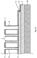
- FIG. 1 is a perspective view showing a configuration of a capacitor device according to a first embodiment.
- FIG. 2 is a diagram showing a part of a longitudinal section taken along line A 1 -A 1 ′ of the capacitor device of FIG. 1 .
- FIG. 3 is a circuit diagram showing an equivalent circuit of the capacitor device of FIG. 2 .
- FIG. 4 is a cross-sectional view showing a first state in the manufacturing process of the capacitor device of FIG. 1 .
- FIG. 5 is a cross-sectional view showing a second state in the manufacturing process of the capacitor device of FIG. 1 .
- FIG. 6 is a cross-sectional view showing a third state in the manufacturing process of the capacitor device of FIG. 1 .
- FIG. 7 is a cross-sectional view showing a fourth state in the manufacturing process of the capacitor device of FIG. 1 .
- FIG. 8 is a cross-sectional view showing a fifth state in the manufacturing process of the capacitor device of FIG. 1 .
- FIG. 9 is a cross-sectional view showing a sixth state in the manufacturing process of the capacitor device of FIG. 1 .
- FIG. 10 is a cross-sectional view showing a seventh state in the manufacturing process of the capacitor device of FIG. 1 .
- FIG. 11 is a cross-sectional view showing an eighth state in the manufacturing process of the capacitor device of FIG. 1 .
- FIG. 12 is a cross-sectional view showing a ninth state in the manufacturing process of the capacitor device of FIG. 1 .
- FIG. 13 is a cross-sectional view showing a tenth state in the manufacturing process of the capacitor device of FIG. 1 .
- FIG. 14 is a perspective view showing a configuration of a capacitor device according to a second embodiment.
- FIG. 15 is a diagram showing a part of a longitudinal section taken along line A 2 -A 2 ′ of the capacitor device of FIG. 12 .
- FIG. 16 is a diagram showing a part of a longitudinal section taken along line A 3 -A 3 ′ of the capacitor device of FIG. 13 .
- FIG. 17 is a circuit diagram showing an equivalent circuit of the capacitor device of FIGS. 15 and 16 .
- FIG. 18 is a top view showing a capacitor device according to a third embodiment in a state where no external terminal is formed.
- FIG. 19 is a top view showing a capacitor device according to a third embodiment in which external terminals 105 and 106 are formed in the capacitor device of FIG. 18 .
- FIG. 20 is a circuit diagram showing an equivalent circuit of the capacitor device of FIG. 18 .
- FIG. 21 is a schematic diagram showing a current flowing through the capacitor device of FIG. 18 .
- FIG. 22 is a top view showing a part of a capacitor device according to a modification of the third embodiment and showing a state in which no external terminal is formed.
- FIG. 23 is a top view showing a configuration of a capacitor device according to a fourth embodiment.
- FIG. 24 is a circuit diagram showing an equivalent circuit of the capacitor device of FIG. 23 .
- FIG. 25 is a top view showing a configuration of a capacitor device according to a fifth embodiment.
- FIG. 26 is a circuit diagram showing an equivalent circuit of the capacitor device of FIG. 25 .
- FIG. 27 is a top view showing a configuration of a capacitor device according to a sixth embodiment.
- FIG. 28 is a circuit diagram showing an equivalent circuit of the capacitor device of FIG. 27 .
- FIG. 29 is a top view showing a configuration of a capacitor device according to a seventh embodiment.
- FIG. 30 is a top view showing a configuration of a capacitor device according to an eighth embodiment.
- FIG. 31 is a top view showing a configuration of a capacitor device according to a ninth embodiment.
- FIG. 32 is a top view showing a configuration of a capacitor device according to a tenth embodiment.
- FIG. 33 is a top view showing a configuration of a capacitor device according to an eleventh embodiment.
- FIG. 34 is a schematic diagram for explaining a method for manufacturing a capacitor device according to third to eleventh embodiments.
- FIG. 35 is a schematic diagram for explaining a method for manufacturing a capacitor device according to third to eleventh embodiments.
- FIG. 1 is a perspective view showing the configuration of the capacitor device according to the first embodiment.
- the capacitor device of FIG. 1 includes a capacitor cell 30 formed on a semiconductor substrate having a first surface and a second surface.
- the lower surface of the capacitor device is a first surface
- the upper surface of the capacitor device is a second surface.
- the capacitor cell 30 includes a first electrode including the metal film 2 , a second electrode including the metal film 9 , and an insulating film (not shown in FIG. 1 ) formed between the first and second electrodes.
- the first electrode including the metal film 2 is also referred to as a lower electrode
- the second electrode including the metal film 9 is also referred to as an upper electrode.
- the capacitor device is electrically connected to the lower electrode including the metal film 2 and electrically connected to at least one first cell terminal including the pad conductor 13 exposed on the upper surface of FIG. 1 and the upper electrode including the metal film 9 . And at least one second cell terminal including a pad conductor 14 exposed on the upper surface shown in the figure.
- the capacitor device includes a plurality of first cell terminals each including a pad conductor 13 and a plurality of second cell terminals each including a pad conductor 14 .
- FIG. 2 is a diagram showing a part of a longitudinal section taken along the line A 1 -A 1 ′ of the capacitor device of FIG. 1 .
- the capacitor device includes an oxide film 1 exposed on the lower surface.
- the oxide film 1 is also referred to as a first silicon oxide film.
- the capacitor device is formed on the oxide film 1 and formed between a lower electrode including a plurality of stacked conductor films, an upper electrode including a plurality of stacked conductor films, and the lower electrode and the upper electrode.
- the insulating film 5 is provided.
- the lower electrode includes a metal film 2 made of tungsten and a conductor film 4 made of Ti—TiN as conductor films.
- the metal film 2 and the conductor film 4 are electrically connected to each other and function as an integrated lower electrode.
- the conductor film 4 functions as a barrier metal.
- the lower electrode further includes a nitride film 3 .
- the upper electrode includes a conductor film 6 made of Ti—TiN, doped silicon 8 and a metal film 9 made of tungsten as conductor films.
- the doped silicon 8 fills the hollow space of the crown type stack capacitor with good coverage and improves its mechanical strength.
- As the doped silicon 8 a boron-doped silicon germanium film may be used.
- the conductor film 6 , the doped silicon 8 , and the metal film 9 are electrically connected to each other and function as an integral upper electrode.
- the upper electrode further includes a nitride film 7 .
- the insulating film 5 is made of, for example, a high dielectric material.
- the insulating film 5 includes, as a high dielectric material, for example, one or more of Ta 2 O 5 material, Al 2 O 3 material, HfO 2 material, ZrO 2 material, and TiO 2 material.
- the lower electrode, the upper electrode, and the insulating film 5 form a capacitor cell 30 . Since each of the lower electrode and the upper electrode includes at least one metal film 2 and 9 , the capacitor cell 30 is formed as an MIM (Metal-Insulator-Metal) capacitor. The capacitor cell 30 is formed as a crown type stack capacitor as shown in FIG. 2 .
- MIM Metal-Insulator-Metal
- the capacitor device includes an interlayer oxide film 12 formed on the metal film 9 of the upper electrode.
- the interlayer oxide film 12 is also referred to as a second silicon oxide film.
- the capacitor device includes a passivation film 15 formed on the interlayer oxide film 12 and exposed on the upper surface.
- the passivation film 15 functions as a protective film that protects the upper surface of the capacitor device.
- the capacitor device is electrically connected to the metal film 2 of the lower electrode and is at least one first cell terminal exposed on the upper surface and electrically connected to the metal film 9 of the upper electrode and exposed at least on the upper surface.
- Each first cell terminal includes a pad conductor 13 exposed on the upper surface and a via conductor 10 electrically connected from the pad conductor 13 to the metal film 2 of the lower electrode.
- the pad conductor 13 is also referred to as a first pad conductor
- the via conductor 10 is also referred to as a first via conductor.
- Each second cell terminal includes a pad conductor 14 exposed on the upper surface and a via conductor 11 electrically connected from the pad conductor 14 to the metal film 9 of the upper electrode.
- the pad conductor 14 is also referred to as a second pad conductor
- the via conductor 11 is also referred to as a second via conductor.
- a barrier metal 21 is formed around the via conductors 10 and 11
- a barrier metal 22 is formed on the lower surfaces of the pad conductors 13 and 14 .
- FIG. 3 is a circuit diagram showing an equivalent circuit of the capacitor device of FIG. 2 .
- the conductor films 4 and 6 are capacitively coupled to each other through the insulating film 5 .
- the conductor film 4 is electrically connected to the pad conductor 13 through the metal film 2 and the via conductor 10 .
- the conductor film 6 is electrically connected to the pad conductor 14 via the doped silicon 8 , the metal film 9 , and the via conductor 11 .
- the capacitor device functions as a capacitor.
- FIG. 4 is a cross-sectional view showing a first state in the manufacturing process of the capacitor device of FIG. 1 .
- FIG. 4 shows a state in which the oxide film 1 and the metal film 2 are formed on the silicon substrate 16 and patterned with a resist mask (not shown).
- a conventional method can be used.
- a thermal oxide film having a high film density may be used as a material that can withstand the mechanical strength at the time of back surface polishing described later.
- FIG. 5 is a cross-sectional view showing a second state in the manufacturing process of the capacitor device of FIG. 1 .
- FIG. 5 shows a state where the nitride film 3 , another oxide film 1 A, and the nitride film 7 are formed after the oxide film 1 and the metal film 2 are formed.
- Prior art methods can be used to form nitride film 3 , another oxide film 1 A, and nitride film 7 .
- the nitride film 7 is formed in order to prevent the crown-type stacked capacitor electrode from falling down in a later step.
- FIG. 6 is a cross-sectional view showing a third state in the manufacturing process of the capacitor device of FIG. 1 .
- FIG. 6 shows a state in which the nitride film 7 , the oxide film 1 A, and the nitride film 3 are patterned and etched to form an opening 17 for the stack capacitor.
- Prior art methods can be used to pattern and etch the nitride film 7 , the oxide film 1 A, and the nitride film 3 .
- FIG. 7 is a cross-sectional view showing a fourth state in the manufacturing process of the capacitor device of FIG. 1 .
- FIG. 7 shows a state in which the conductor film 4 is formed and the oxide film 18 is further formed.
- Prior art methods can be used to form the conductor film 4 and the oxide film 18 .
- FIG. 8 is a sectional view showing a fifth state in the manufacturing process of the capacitor device of FIG. 1 .
- FIG. 8 shows a state in which the opening 20 for forming the crown type stack capacitor is patterned by the photoresist 19 .
- FIG. 9 is a sectional view showing a sixth state in the manufacturing process of the capacitor device of FIG. 1 .
- FIG. 9 shows a state in which the photoresist 19 is removed after the oxide film 18 in the opening 20 is etched. Thereafter, the conductor film 4 and the nitride film 7 in the opening 20 are etched using the oxide film 18 as a mask (not shown). At this time, the oxide film 18 and the conductor film 4 serving as a mask are also removed in a self-aligned manner, and a remaining structure of the conductor film 4 forms a crown-shaped structure. Even if the conductor film 4 that becomes a mask remains after etching, it can be removed by performing additional etching only on the conductor film 4 .
- FIG. 10 is a sectional view showing a seventh state in the manufacturing process of the capacitor device of FIG. 1 .
- FIG. 10 shows a state in which the oxide film 1 A remaining immediately under the side wall of the conductor film 4 and the nitride film 7 is removed from the opening formed at the position of the opening 20 in FIG. 9 by a wet process.
- a lower electrode including the metal film 2 and the conductor film 4 as a plurality of stacked conductor films is formed on the oxide film 1 .
- FIG. 11 is a sectional view showing an eighth state in the manufacturing process of the capacitor device of FIG. 1 .
- the insulating film 5 is formed on the conductor film 4 , and the conductor film 6 , the doped silicon 8 , and the metal film 9 are sequentially formed on the insulating film 5 , and then the insulating film 5 , the doped silicon is formed. 8 and the metal film 9 are patterned by etching.
- a conventional method can be used.
- the insulating film 5 is formed on the lower electrode, and the upper electrode including the conductor film 6 , the doped silicon 8 , and the metal film 9 is formed on the insulating film 5 as a plurality of stacked conductor films. Is done.
- FIG. 12 is a cross-sectional view showing a ninth state in the manufacturing process of the capacitor device of FIG. 1 .
- FIG. 12 shows a state in which an interlayer oxide film 12 is formed and planarized on the nitride film 3 and the metal film 9 of the upper electrode.
- Prior art methods can be used to form and planarize the interlayer oxide film 12 .
- the planarization may be performed using a chemical mechanical polishing technique, may be performed by removing only the oxide film on the convex portion by patterning and etching, or a combination thereof.
- FIG. 13 is a cross-sectional view showing a tenth state in the manufacturing process of the capacitor device of FIG. 1 .
- via conductors 10 and 11 penetrating the interlayer oxide film 12 are formed, pad conductors 13 and 14 are formed on the interlayer oxide film 12 , and a passivation film 15 is formed on the interlayer oxide film 12 . Shows the state. In the passivation film 15 , openings are formed only in the portions of the pad conductors 13 and 14 .
- Prior art methods can be used to form via conductors 10 and 11 .
- the via conductor 10 and the pad conductor 13 are electrically connected to the metal film 2 of the lower electrode and form at least one first cell terminal exposed on the upper surface.
- the via conductor 11 and the pad conductor 14 are electrically connected to the metal film 9 of the upper electrode and form at least one second cell terminal exposed on the upper surface.
- a barrier metal 21 is formed around the via conductors 10 and 11 , and a barrier metal 22 is formed on the lower surfaces of the pad conductors 13 and 14 .
- the silicon substrate 16 is removed by backside polishing, whereby the capacitor device of FIG. 2 is completed.
- the capacitor device according to the first embodiment does not use a silicon substrate in the portion of the capacitor cell 30 , the capacitor device operates normally even if the silicon substrate 16 is removed by backside polishing. By removing the silicon substrate 16 , the thickness of the capacitor device can be reduced as compared with the conventional case.
- the total thickness of the capacitor device according to the first embodiment can be reduced to about 4 to 5 ⁇ m when configured as a MIM crown type stack capacitor.
- a concave (Concaved) stack MIM capacitor according to the prior art may be adopted.
- An advantage of the MIM capacitor is that the desired capacitance can be secured without increasing the thickness of the capacitor device due to the effect of the high dielectric constant of the insulating film.
- a capacitor can be formed without using a structure formed below the surface of a silicon substrate like a trench capacitor, and is very suitable for thinning the capacitor device itself. Furthermore, process development costs can be reduced by diverting general-purpose DRAM semiconductor process technology.
- FIG. 14 is a perspective view showing the configuration of the capacitor device according to the second embodiment.
- the capacitor device of FIG. 14 is configured similarly to the capacitor cell 30 of the capacitor device according to the first embodiment, and a plurality of capacitor cells 30 - 1 stacked in a direction perpendicular to the lower surface and the upper surface of the semiconductor substrate. And 30 - 2 .
- At least one first cell terminal including the pad conductor 13 is electrically connected to the lower electrode including the metal film 2 - 1 in the capacitor cell 30 - 1 , and further, the metal film 2 in the capacitor cell 30 - 2 . 2 is electrically connected to the lower electrode.
- At least one second cell terminal including the pad conductor 14 is electrically connected to the upper electrode including the metal film 9 - 1 in the capacitor cell 30 - 1 , and further, the metal film 9 - 2 in the capacitor cell 30 - 2 .
- FIG. 15 is a view showing a part of a longitudinal section taken along line A 2 -A 2 ′ of the capacitor device of FIG. 14 .
- FIG. 16 is a view showing a part of a longitudinal section taken along line A 3 -A 3 ′ of the capacitor device of FIG. 14 .
- the capacitor device of FIG. 14 forms the capacitor cell 30 in FIG. 11 , forms the interlayer oxide film 12 in FIG. 12 and planarizes the upper surface, and then repeats the steps described with reference to FIG. 4 to FIG. 12 . Repeatedly, another capacitor cell 30 is formed.
- a plurality of capacitor cells 30 - 1 and 30 - 2 are formed that are stacked in a direction perpendicular to the lower surface and the upper surface of the semiconductor substrate.
- the silicon substrate 16 is removed by backside polishing.
- the via conductor 10 is electrically connected to the metal film 2 - 1 of the lower electrode in the capacitor cell 30 - 1 , and further electrically connected to the metal film 2 - 2 of the lower electrode in the capacitor cell 30 - 2 . It is formed to be connected. Accordingly, the first cell terminal including the via conductor 10 and the pad conductor 13 is connected to the lower electrodes of the plurality of capacitor cells 30 - 1 and 30 - 2 .
- Via conductor 11 is electrically connected to metal film 9 - 1 of the upper electrode in capacitor cell 30 - 1 , and is further electrically connected to metal film 9 - 2 of the upper electrode in capacitor cell 30 - 2 .
- the second cell terminal including the via conductor 11 and the pad conductor 14 is connected to the upper electrodes of the plurality of capacitor cells 30 - 1 and 30 - 2 .
- FIG. 17 is a circuit diagram showing an equivalent circuit of the capacitor device of FIGS. 15 and 16 .
- the conductor films 4 - 1 and 6 - 1 are capacitively coupled to each other through the insulating film 5 - 1 .
- the conductor film 4 - 1 is electrically connected to the pad conductor 13 through the metal film 2 - 1 and the via conductor 10 .
- the conductor film 6 - 1 is electrically connected to the pad conductor 14 via doped silicon (not shown), the metal film 9 - 1 , and the via conductor 11 .
- the conductor films 4 - 2 and 6 - 2 are capacitively coupled to each other through the insulating film 5 - 2 .
- the conductor film 4 - 2 is electrically connected to the pad conductor 13 through the metal film 2 - 2 and the via conductor 10 .
- the conductor film 6 - 2 is electrically connected to the pad conductor 14 via doped silicon (not shown), the metal film 9 - 2 , and the via conductor 11 . Thereby, the capacitor cells 30 - 1 and 30 - 2 are connected in parallel between the pad conductors 13 and 14 .
- the capacitor cells 30 - 1 and 30 - 2 are stacked and connected in parallel, so that the area of the capacitor cell in the horizontal direction is not increased.
- the capacity can be doubled.
- the via conductors 10 and 11 may be formed using, for example, a conventional TSV (Through Si Via) technique.
- the thickness of the capacitor device can be reduced as compared with the conventional case by removing the silicon substrate, similarly to the capacitor device according to the first embodiment.
- the total thickness of the capacitor device according to the second embodiment is only about 6 to 7 ⁇ m when configured as a MIM crown type stack capacitor.
- the capacitor device according to the second embodiment also has other advantages similar to those of the capacitor device according to the first embodiment.
- FIG. 18 is a top view showing the capacitor device according to the third embodiment, in which no external terminal is formed.
- the capacitor device of FIG. 18 includes a plurality of capacitor cells C formed on a rectangular semiconductor substrate having sides extending along a first direction and a second direction orthogonal to each other.
- FIG. 18 includes a plurality of lower electrodes 101 , a plurality of upper electrodes 102 , a plurality of cell terminals 103 , and a plurality of cell terminals 104 formed on a semiconductor substrate.
- Each lower electrode 101 , each upper electrode 102 , each cell terminal 103 , and each cell terminal 104 are the lower electrode, the upper electrode, the first cell terminal, and the second electrode of the capacitor device according to the first embodiment. It corresponds to each cell terminal.
- Each lower electrode 101 , each upper electrode 102 , each cell terminal 103 , and each cell terminal 104 are formed on a semiconductor substrate including an oxide film, as in the capacitor device according to the first embodiment. After FIG. 18 , the semiconductor substrate is omitted for simplification of illustration.
- each lower electrode 101 , each upper electrode 102 , each cell terminal 103 , and each cell terminal 104 is referred to as a first electrode, a second electrode, a first cell terminal, and a second cell terminal. Also called a cell terminal.
- the plurality of lower electrodes 101 includes a portion (for example, a portion corresponding to the metal film 2 in FIG. 2 ) formed in the first layer of the semiconductor substrate, and is disposed at the first period d 1 in the X direction. Arranged in the direction with a second period d 2 .
- the plurality of upper electrodes 102 include a portion (for example, a portion corresponding to the metal film 9 in FIG. 2 ) formed in a second layer different from the first layer of the semiconductor substrate, and is arranged with a period d 1 in the X direction, and arranged with a period d 2 in the Y direction.
- Each upper electrode 102 is arranged so as to be shifted from the lower electrode 101 by a half of the length of the period d 1 in the X direction, and is shifted by a half of the length of the period d 2 in the Y direction.
- Each lower electrode 101 and each upper electrode 102 are partly opposed and capacitively coupled to each other, and each pair of lower electrode 101 and upper electrode 102 that are capacitively coupled to each other form a capacitor cell C.
- the plurality of cell terminals 103 includes a portion formed in a third layer different from the first and second layers of the semiconductor substrate, and is arranged with a period d 1 in the X direction and with a period d 2 in the Y direction.
- the plurality of lower electrodes 101 are electrically connected to each other.
- the second layer is located between the first and third layers.
- the plurality of cell terminals 104 include a portion formed in the third layer of the semiconductor substrate, and are arranged with a period d 1 in the X direction and with a period d 2 in the Y direction, and are electrically connected to the plurality of upper electrodes 102 , respectively.
- Each cell terminal 104 is arranged so as to be shifted from the cell terminal 103 by half the length of the period d 1 in the X direction, and is shifted by half the length of the period d 2 in the Y direction.
- the capacitor device includes two lower electrodes 101 adjacent to each other in the Y direction and two upper electrodes 102 adjacent to each other in the X direction (or two lower electrodes 101 adjacent to each other in the X direction; A plurality of unit cells 100 (including two upper electrodes 102 adjacent to each other in the Y direction) are included.
- Each unit cell 100 includes four capacitor cells C formed from a pair of lower electrode 101 and upper electrode 102 that are capacitively coupled to face each other. Capacitor cells C having a desired number of rows and columns are formed by repeatedly arranging a plurality of unit cells 100 .
- the capacitor device according to the third embodiment may be configured similarly to the capacitor device according to the first embodiment.
- the semiconductor substrate has a first surface and a second surface.
- the capacitor device includes a first silicon oxide film exposed on the first surface and a passivation film exposed on the second surface.
- Each lower electrode 101 is formed on the first silicon oxide film and includes a plurality of stacked conductor films.
- Each upper electrode 102 includes a plurality of stacked conductor films.
- the capacitor device further includes an insulating film formed between each lower electrode 101 and each upper electrode 102 and a second silicon oxide film formed on each upper electrode 102 .
- the passivation film is formed on the second silicon oxide film.
- Cell terminals 103 and 104 are exposed on the second surface.
- Each capacitor cell C is formed of a pair of lower electrode 101 and upper electrode 102 that are capacitively coupled to face each other, and an insulating film formed therebetween.
- Each capacitor cell C may be formed as a crown type stack capacitor.
- Each of the cell terminals 103 and 104 may be configured similarly to the first and second cell terminals of the capacitor device according to the first embodiment.
- each cell terminal 103 is electrically connected to the first pad conductor formed on the third layer of the semiconductor substrate and one of the plurality of lower electrodes 101 from the first pad conductor.
- each cell terminal 104 is electrically connected to a second pad conductor formed on the third layer of the semiconductor substrate and one of the plurality of upper electrodes 102 from the second pad conductor.
- FIG. 19 is a top view showing the capacitor device according to the third embodiment, in which external terminals 105 and 106 are formed in the capacitor device of FIG. 18 .
- the capacitor device further includes at least two external terminals 105 and 106 for electrical connection to a circuit external to the capacitor device.
- Each external terminal 105 and 106 is electrically connected to a part of the plurality of cell terminals including the plurality of cell terminals 103 and the plurality of cell terminals 104 , respectively.
- the plurality of cell terminals 103 and 104 extend in the Y direction, and form a plurality of cell terminal rows adjacent to each other in the extending direction.
- the capacitor device includes external terminals 105 and 106 each having a comb shape.
- the external terminal 105 includes a plurality of first portions (portions extending in the Y direction) electrically connected to every 2N cell terminal rows of the plurality of cell terminal rows when N is an integer, and a second portion (a portion extending in the X direction) that connects the first portions to each other.
- the external terminal 106 also includes a plurality of first portions (portions extending in the Y direction) electrically connected to every 2N cell terminal rows of the plurality of cell terminal rows, and a first portion, and a second portion (a portion extending in the X direction) connected to each other.
- Each first portion of the external terminal 105 and each first portion of the external terminal 106 are formed so as to be fitted to each other.
- Each of the external terminals 105 and 106 is arranged such that every N cell terminal rows of the plurality of cell terminal rows are electrically connected to the external terminals 105 and 106 alternately.
- the external terminals 105 and 106 can be connected to a voltage source having an arbitrary voltage. For example, one of them may be connected to a power source and the other may be grounded.
- the external terminals 105 and 106 are electrically connected to a circuit external to the capacitor device at a portion electrically connected to one of the plurality of cell terminal rows (that is, each first portion of the external terminals 105 and 106 ). Instead, the external terminals 105 and 106 may be electrically connected to a circuit outside the capacitor device in their respective second portions (portions extending in the X direction).
- FIG. 20 is a circuit diagram showing an equivalent circuit of the capacitor device of FIG. 18 .
- each capacitor cell C is formed between each pair of the lower electrode 101 and the upper electrode 102 that are capacitively coupled to face each other.
- one capacitor cell C is formed between the external terminals 105 and 106 adjacent to each other. Therefore, in the entire capacitor device, a plurality of capacitor cells C are connected in parallel.
- FIG. 21 is a schematic diagram showing a current flowing through the capacitor device of FIG. 18 .
- the external terminals 105 and 106 are omitted.
- the equivalent series inductance ESL
- the equivalent series inductance can be reduced by arranging each lower electrode 101 , each upper electrode 102 , each cell terminal 103 , and each cell terminal 104 periodically and symmetrically.
- the equivalent series inductance is best reduced when a fine pitch bump is formed in a portion where the external terminals 105 and 106 are electrically connected to one of the plurality of cell terminal rows.
- each lower electrode 101 , each upper electrode 102 , each cell terminal 103 , and each cell terminal 104 are arranged in the X direction and the period d 2 in which each cell terminal 104 is arranged in the Y direction may be set to be equal to each other.
- FIG. 22 is a top view showing a part of a capacitor device according to a modification of the third embodiment and showing a state in which no external terminal is formed.
- the period d 1 ′ in which the upper electrodes 102 , the cell terminals 103 , and the cell terminals 104 are arranged in the X direction and the period d 2 ′ in the Y direction are set to be different from each other.
- the unit cell 100 A includes two lower electrodes 101 adjacent in the Y direction and two upper electrodes 102 adjacent in the X direction.
- the capacitor device of FIG. 22 can also operate in the same manner as the capacitor device of FIG. 18 .
- a capacitor device having characteristics such as a different capacitance, a different capacitance density, a different breakdown voltage, and/or a different position and number of terminals from the capacitor device of FIG. 19 .
- a mask for forming the external terminals 105 and 106 may be replaced as described in the following embodiments.
- a plurality of expensive masks are required.
- the capacitor device according to the third embodiment when customizing the capacitor device according to customer requirements, by changing only one (or a small number) of relatively inexpensive masks, the external terminals 105 and 106 can be changed. The shape can be changed, whereby the characteristics of the capacitor described above can be changed. At this time, it is not necessary to change the mask for forming the plurality of capacitor cells C.
- FIG. 23 is a top view showing the configuration of the capacitor device according to the fourth embodiment.
- the capacitor device of FIG. 23 includes external terminals 105 A and 106 A each having a comb shape.
- Each of the external terminals 105 A and 106 A is arranged such that every two cell terminal rows of the plurality of cell terminal rows are electrically connected to the external terminals 105 A and 106 A alternately.
- the capacitor device of FIG. 23 further includes a plurality of floating terminals 107 that are electrically connected to the cell terminal row including the cell terminals 103 that are not connected to the external terminals 105 A and 106 A, due to the convenience of the semiconductor process technology. Each floating terminal 107 is not connected to other circuits.
- FIG. 24 is a circuit diagram showing an equivalent circuit of the capacitor device of FIG. 23 .
- two capacitor cells C are formed between the external terminals 105 A and 106 A adjacent to each other. Therefore, in the entire capacitor device, a plurality of circuits each including two capacitor cells C connected in series are connected in parallel.
- FIG. 25 is a top view showing the configuration of the capacitor device according to the fifth embodiment.
- the capacitor device of FIG. 25 includes external terminals 105 B and 106 B each having a comb shape.
- the external terminals 105 B extend in the Y direction and are electrically connected to every six cell terminal rows among the plurality of adjacent cell terminal rows, and the external terminal 106 B also has a plurality of cell terminals. It is electrically connected to every six cell terminal rows in the row.
- Each of the external terminals 105 B and 106 B is arranged such that every three cell terminal rows of the plurality of cell terminal rows are electrically connected to the external terminals 105 B and 106 B alternately.
- the capacitor device of FIG. 25 further includes a plurality of floating terminals 107 and 108 that are electrically connected to cell terminal rows that are not connected to the external terminals 105 B and 106 B, respectively, for the convenience of semiconductor process technology.
- Each floating terminal 107 is electrically connected to a cell terminal row including cell terminals 103
- each floating terminal 108 is electrically connected to a cell terminal row including cell terminals 104 .
- Each floating terminal 107 and 108 is not connected to other circuits.
- FIG. 26 is a circuit diagram showing an equivalent circuit of the capacitor device of FIG. 25 .
- three capacitor cells C are formed between the external terminals 105 B and 106 B adjacent to each other. Therefore, in the entire capacitor device, a plurality of circuits each including three capacitor cells C connected in series are connected in parallel.
- FIG. 27 is a top view showing the configuration of the capacitor device according to the sixth embodiment.
- the capacitor device of FIG. 27 includes external terminals 105 C and 106 C each having a comb shape.
- Each of the external terminals 105 C and 106 C is arranged such that every four cell terminal rows of the plurality of cell terminal rows are electrically connected to the external terminals 105 C and 106 C alternately.
- the capacitor device of FIG. 27 further includes a plurality of floating terminals 107 and 108 that are electrically connected to cell terminal rows that are not connected to the external terminals 105 C and 106 C, respectively, due to the convenience of semiconductor process technology.
- Each floating terminal 107 is electrically connected to a cell terminal row including cell terminals 103
- each floating terminal 108 is electrically connected to a cell terminal row including cell terminals 104 .
- Each floating terminal 107 and 108 is not connected to other circuits.
- FIG. 28 is a circuit diagram showing an equivalent circuit of the capacitor device of FIG. 27 .
- four capacitor cells C are formed between the external terminals 105 C and 106 C adjacent to each other. Therefore, in the entire capacitor device, a plurality of circuits each including four capacitor cells C connected in series are connected in parallel.
- a pair of external terminals includes a pair of cell terminal rows every N of the plurality of cell terminal rows. You may arrange
- the number of capacitor cells C connected in series can be changed by changing the shape of the external terminal.
- the number of capacitor cells C connected in series is inversely proportional to the capacity density and breakdown voltage of the capacitor device.
- FIG. 29 is a top view showing the configuration of the capacitor device according to the seventh embodiment.
- the plurality of external terminals 105 and 106 are not limited to being formed in the same layer.
- the external terminal 105 is formed below the lower electrode 101
- the external terminal 106 is formed above the upper electrode 102 .
- the capacitor device according to the seventh embodiment can also operate in the same manner as the capacitor device according to the third embodiment.
- FIG. 30 is a top view showing the configuration of the capacitor device according to the eighth embodiment.
- the plurality of cell terminals 103 and 104 extend in the X direction and are adjacent to each other in the extending direction instead of the cell terminal rows extending in the Y direction as in the third to seventh embodiments.
- the cell terminal array may be formed.
- the capacitor device includes external terminals 105 D and 106 D each having a comb shape.
- the external terminal 105 D has a plurality of first portions (portions extending in the X direction) electrically connected to every 2N cell terminal rows of the plurality of cell terminal rows when N is an integer, and a second portion (a portion extending in the Y direction) that connects the first portions to each other.
- the external terminal 106 D also includes a plurality of first portions (portions extending in the X direction) electrically connected to every 2N cell terminal rows of the plurality of cell terminal rows, and a first portion, and a second portion (a portion extending in the Y direction) connected to each other.
- Each first portion of the external terminal 105 D and each first portion of the external terminal 106 D are formed so as to be fitted to each other.
- Each of the external terminals 105 D and 106 D is arranged such that every N cell terminal rows of the plurality of cell terminal rows are electrically connected to the external terminals 105 D and 106 D alternately.
- the external terminals 105 D and 106 D are electrically connected to a circuit outside the capacitor device in a portion electrically connected to one of the plurality of cell terminal rows (that is, each first portion of the external terminals 105 D and 106 D). May be connected. Instead, the external terminals 105 D and 106 D may be electrically connected to a circuit outside the capacitor device in their respective second portions (portions extending in the Y direction).
- a pair of external terminals includes a pair of cell terminal rows every N of the plurality of cell terminal rows. You may arrange
- the capacitor device according to the eighth embodiment has an effect that the shape of the external terminal and the position at which the external terminal is electrically connected to a circuit outside the capacitor device can be customized according to customer requirements.
- the capacitor device may include external terminals 105 D and 106 D formed as in the eighth embodiment, and these external terminals 105 D and 106 D are short sides (sides extending in the Y direction) of the rectangular capacitor device, may be electrically connected to a circuit outside the capacitor device.
- the capacitor device may include external terminals 105 and 106 formed as in the third to seventh embodiments, and these external terminals 105 and 106 are the length of the rectangular capacitor device.
- the side (side extending in the X direction) may be electrically connected to a circuit outside the capacitor device.
- the equivalent series inductance is higher in the third to seventh embodiments than in the case where the short side of the rectangular capacitor device is electrically connected to a circuit outside the capacitor device as in the eighth embodiment.
- the case where the long side of the rectangular capacitor device is electrically connected to a circuit outside the capacitor device is reduced.
- FIG. 31 is a top view showing the configuration of the capacitor device according to the ninth embodiment.
- the plurality of cell terminals 103 and 104 extend in the Y direction, and form a plurality of cell terminal rows adjacent to each other in the extending direction.
- the capacitor device includes external terminals 111 and 112 each having a comb shape, and an external terminal 113 having a fishbone shape.
- the external terminal 113 includes a plurality of first portions (portions extending in the Y direction) electrically connected to every 2N cell terminal rows of the plurality of cell terminal rows when N is an integer, and a second portion (a portion extending in the X direction) for connecting the first portions of the external terminals 113 to each other at the center of the first portions of the external terminals 113 .
- the external terminal 111 includes a plurality of first portions (extending in the Y direction) that are electrically connected to a part of the plurality of cell terminals included in every 2N cell terminal rows of the plurality of cell terminal rows, and a second portion (a portion extending in the X direction) that connects the first portions of the external terminals 111 to each other.
- the external terminal 111 is formed on the first side with respect to the second portion of the external terminal 113 so as to be fitted to the first portion of the external terminal 113 .
- the external terminal 112 includes a plurality of first portions (extending in the Y direction) that are electrically connected to a part of the plurality of cell terminals included in every 2N cell terminal rows of the plurality of cell terminal rows, and a second portion (a portion extending in the X direction) that connects the first portions of the external terminals 112 to each other.
- the external terminal 112 is formed to be fitted to the first portion of the external terminal 113 on the second side opposite to the first side with respect to the second portion of the external terminal 113 .
- Each of the external terminals 111 to 113 is arranged such that every N cell terminal rows of the plurality of cell terminal rows are electrically connected to the external terminals 111 and 112 and the external terminal 113 alternately.
- the external terminal 111 is electrically connected to a part of the plurality of cell terminals included in every two cell terminal rows of the plurality of cell terminal rows.
- Each of the external terminals 112 to 113 electrically connected to a part of the plurality of cell terminals included in every two cell terminal columns of the plurality of cell terminal columns which are arranged so as to be electrically connected to the external terminals 111 and 112 and the external terminal 113 alternately.
- the external terminals 111 and 112 may be electrically connected to a circuit outside the capacitor device on the long side (side extending in the X direction) of the capacitor device.
- the external terminal 113 may be electrically connected to a circuit outside the capacitor device on the short side (side extending in the Y direction) of the capacitor device.
- the external terminal 113 is connected to a power source, for example, and the external terminals 111 and 112 are grounded, for example.
- the capacitor device according to the ninth embodiment has an effect of reducing the equivalent series inductance compared to the third to eighth embodiments by changing the shape of the external terminal.
- FIG. 32 is a top view showing the configuration of the capacitor device according to the tenth embodiment.
- the plurality of cell terminals 103 and 104 extend in the Y direction, and form a plurality of cell terminal rows adjacent to each other in the extending direction.
- the capacitor device includes external terminals 111 A and 112 A each having a comb shape, and an external terminal 113 A having a meander shape.
- the external terminal 113 A has a plurality of first portions (portions extending in the Y direction) electrically connected to every 2N cell terminal rows of the plurality of cell terminal rows when N is an integer.
- the external terminal 111 A includes a plurality of first portions (portions extending in the Y direction) electrically connected to every 4N cell terminal rows of the plurality of cell terminal rows, and each of the external terminals 111 A.
- the external terminal 111 A is formed on the first side with respect to the external terminal 113 A so as to be fitted to the first portion of the external terminal 113 A.
- the external terminal 112 A includes a plurality of first portions (portions extending in the Y direction) electrically connected to every 4N cell terminal rows of the plurality of cell terminal rows, and each of the external terminals 112 A, and a second portion (a portion extending in the X direction) that connects the first portions to each other.
- the external terminal 112 A is formed to be fitted to the first portion of the external terminal 113 A on the second side opposite to the first side with respect to the external terminal 113 A.
- Each of the external terminals 111 A to 113 A is arranged such that every N cell terminal rows of the plurality of cell terminal rows are electrically connected to the external terminals 111 A or 112 A and the external terminals 113 A alternately.
- the external terminal 111 A is electrically connected to every four cell terminal rows of the plurality of cell terminal rows.
- the external terminal 112 A is electrically connected to every four cell terminal rows of the plurality of cell terminal rows.
- Each of the external terminals 111 A to 113 A is arranged such that a plurality of cell terminal arrays are alternately electrically connected to the external terminals 111 A or 112 A and the external terminals 113 A.
- the external terminals 111 A and 112 A may be electrically connected to a circuit outside the capacitor device on the long side (side extending in the X direction) of the capacitor device.
- the external terminal 113 A may be electrically connected to a circuit outside the capacitor device on the short side (side extending in the Y direction) of the capacitor device.
- the external terminal 113 A is connected to a power source, for example, and the external terminals 111 A and 112 A are grounded, for example.
- the capacitor device of the tenth embodiment by changing the shape of the external terminal, it is equivalent to the third to eighth embodiments as in the case of the ninth embodiment. There is an effect of reducing the series inductance.
- FIG. 33 is a top view showing the configuration of the capacitor device according to the eleventh embodiment.
- the capacitor device may include four or more external terminals.
- the plurality of cell terminals 103 and 104 extend in the Y direction, and form a plurality of cell terminal rows adjacent to each other in the extending direction.
- the capacitor device includes a plurality of sets of external terminals each including first and second external terminals.
- a set including the external terminals 121 and 125 , a set including the external terminals 122 and 126 , a set including the external terminals 123 and 126 , and a set including the external terminals 124 and 127 are provided.
- Each of the first and second external terminals of each set includes a portion that is electrically connected to at least one cell terminal row of the plurality of cell terminal rows.
- Each of the first and second external terminals of each set is such that when N is an integer, every N cell terminal rows of the plurality of cell terminal rows are alternately connected to the first and second external terminals, arranged to be connected to each other.
- the external terminals 125 to 127 are connected to a power source, for example, and the external terminals 121 to 124 are grounded, for example.
- a plurality of cell terminal arrays are alternately electrically connected to the external terminals 125 to 127 connected to the power source and the grounded external terminals 121 to 124 .
- the external terminals 125 and 126 connected to the power source and the external terminals 122 and 124 grounded are alternately provided on the +Y side.
- the external terminals 126 and 127 connected to the power source and the external terminals 121 and 123 connected to the ground alternately on the ⁇ Y side side.
- the capacitor device according to the eleventh embodiment has an effect of further reducing the equivalent series inductance compared to the ninth and tenth embodiments by changing the shape of the external terminal.
- the capacitor devices according to the third to eleventh embodiments can be manufactured, for example, by the following manufacturing process.
- the manufacturing method includes a plurality of lower electrodes 101 including a portion formed in a first layer of a semiconductor substrate, arranged at a period d 1 in the X direction and arranged at a period d 2 in the Y direction.
- a plurality of upper electrodes including a step of forming an electrode 101 and a portion formed in a second layer different from the first layer of the semiconductor substrate, the electrodes being arranged at a period d 1 in the X direction, and in the Y direction; forming a plurality of upper electrodes 102 arranged at a period d 2 .
- the step of forming each upper electrode 102 is arranged so as to be shifted by half the length of the period d 1 in the X direction with respect to each lower electrode 101 and shifted by half the length of the period d 2 in the Y direction.
- Each lower electrode 101 and each upper electrode 102 are partly opposed and capacitively coupled to each other, and each pair of lower electrode 101 and upper electrode 102 that are capacitively coupled to each other form a capacitor cell C.
- the manufacturing method includes a plurality of cell terminals 103 including a portion formed in a third layer different from the first and second layers of the semiconductor substrate, arranged at a period d 1 in the X direction, and a period in the Y direction.
- the second layer is located between the first and third layers.
- the step of forming each cell terminal 104 is arranged with respect to each cell terminal 103 by being shifted by half the length of the period d 1 in the X direction and by being shifted by half the length of the period d 2 in the Y direction.
- the manufacturing method further includes forming at least two external terminals that are respectively electrically connected to a part of the plurality of cell terminals including the plurality of cell terminals 103 and the plurality of cell terminals 104 .
- FIGS. 34 and 35 are schematic views for explaining the capacitor device manufacturing method according to the third to eleventh embodiments.
- a capacitor device of a type called MLCC multilayer ceramic capacitor
- MLCC multilayer ceramic capacitor
- Many of such capacitor devices have a rectangular parallelepiped outer shape and are external terminals having the shapes described in the third to eleventh embodiments, and have been described in the third to eleventh embodiments.
- an external terminal connected to an external circuit is provided.
- Various configurations can be taken by providing compatibility with MLCC when mounting the capacitor device and changing only one mask to meet customer requirements.
- MLCC capacitor devices are available in various sizes.
- a scribe line and a guard ring are arranged so that a chip having the smallest size can be cut out from a silicon wafer.
- the size of the capacitor device can be changed by changing only three masks as described below. Thereafter, by removing the scribe line and the guard ring, it is possible to connect the chips of each capacitor device with metal wiring. For this reason, the size of the capacitor device can be changed to be scalable.
- metal wiring 211 used as a scribe line and a guard ring is formed on a semiconductor substrate in the manufacturing process of the capacitor device.
- the capacitor device region 201 has, for example, a 05025 size (500 ⁇ 250 ⁇ m).
- a metal wiring 212 is formed on the semiconductor substrate.
- the region 202 of the capacitor device having a 1005 size (1000 ⁇ 500 ⁇ m) can be obtained.
- the manufacturing method performs the following steps according to a desired position where the external terminal is electrically connected to a circuit outside the capacitor device, a desired capacitance and desired breakdown voltage of the capacitor device, and a size of the capacitor device. That is, the manufacturing method includes a step of selecting a first mask for forming a metal wiring used as a scribe line and a guard ring, a step of selecting a second mask for forming an external terminal, selecting a third mask for forming a cell terminal for connecting the metal wiring and the external terminal to each other among the cell terminals.
- the capacitor devices according to the third to eleventh embodiments only a small number of masks need be changed, so that the design change of the capacitor device can be performed at low cost.
- the number of rows and/or columns of the capacitor cell C of the capacitor device is equal to the number of capacitor cells connected in series required for each application, set to least common multiple or multiple.
- the capacitor device according to each embodiment of the present invention is useful, for example, as an on-package decoupling capacitor.
- semiconductor devices there are problems such as a decrease in voltage tolerance range due to a decrease in power supply voltage, generation of large power supply noise or ground noise due to an increase in current consumption, and a decrease in EMI resistance due to an increase in operating frequency.
- problems such as a decrease in voltage tolerance range due to a decrease in power supply voltage, generation of large power supply noise or ground noise due to an increase in current consumption, and a decrease in EMI resistance due to an increase in operating frequency.
- it is effective to use a decoupling capacitor.
- By using the capacitor device according to each embodiment of the present invention it is possible to provide a semiconductor device in which the above problems are reduced.
Abstract
Description
- 1, 1A . . . Oxide film,
- 2, 2-1, 2-2 . . . Metal film,
- 3 . . . Nitride film,
- 4, 4-1, 4-2 . . . Conductor film,
- 5, 5-1, 5-2 . . . Insulating film,
- 6, 6-1, 6-2 . . . conductor film,
- 7 . . . nitride film,
- 8 . . . doped silicon,
- 9, 9-1, 9-2 . . . metal film,
- 10 . . . via conductor,
- 11 . . . via conductor,
- 12 . . . Interlayer oxide film,
- 13 . . . pad conductor,
- 14 . . . pad conductor,
- 15 . . . passivation film,
- 16 . . . silicon substrate,
- 17 . . . opening,
- 18 . . . oxide film,
- 19 . . . photoresist,
- 20 . . . opening,
- 21 . . . barrier metal,
- 22 . . . Barrier metal,
- 30, 30-1, 30-2 . . . Capacitor cell,
- 100, 100A . . . Unit cell,
- 101 . . . Lower electrode,
- 102 . . . Upper electrode,
- 103 . . . Cell terminal,
- 104 . . . Cell terminal,
- 105, 105 a˜105D . . . external terminals,
- 106, 106 a˜106D . . . external terminals,
- 107, 108 . . . floating terminals,
- 111˜113, 121˜127 . . . external terminals,
- 201, 202 . . . area of the capacitor device,
- 211, 212 . . . metal wiring.
Claims (18)
Applications Claiming Priority (1)
| Application Number | Priority Date | Filing Date | Title |
|---|---|---|---|
| PCT/JP2017/016977 WO2018198330A1 (en) | 2017-04-28 | 2017-04-28 | Capacitor device and manufacturing method therefor |
Related Parent Applications (1)
| Application Number | Title | Priority Date | Filing Date |
|---|---|---|---|
| PCT/JP2017/016977 A-371-Of-International WO2018198330A1 (en) | 2017-04-28 | 2017-04-28 | Capacitor device and manufacturing method therefor |
Related Child Applications (1)
| Application Number | Title | Priority Date | Filing Date |
|---|---|---|---|
| US17/085,770 Continuation-In-Part US20210050410A1 (en) | 2017-04-28 | 2020-10-30 | Capacitor device and manufacturing method therefor |
Publications (2)
| Publication Number | Publication Date |
|---|---|
| US20200098853A1 US20200098853A1 (en) | 2020-03-26 |
| US11038012B2 true US11038012B2 (en) | 2021-06-15 |
Family
ID=63918104
Family Applications (1)
| Application Number | Title | Priority Date | Filing Date |
|---|---|---|---|
| US16/609,159 Active 2037-07-03 US11038012B2 (en) | 2017-04-28 | 2017-04-28 | Capacitor device and manufacturing method therefor |
Country Status (3)
| Country | Link |
|---|---|
| US (1) | US11038012B2 (en) |
| JP (1) | JP6639736B2 (en) |
| WO (1) | WO2018198330A1 (en) |
Families Citing this family (10)
| Publication number | Priority date | Publication date | Assignee | Title |
|---|---|---|---|---|
| US11158552B2 (en) | 2018-12-26 | 2021-10-26 | AP Memory Technology Corp. | Semiconductor device and method to manufacture the same |
| US11380614B2 (en) | 2018-12-26 | 2022-07-05 | AP Memory Technology Corp. | Circuit assembly |
| US11417628B2 (en) | 2018-12-26 | 2022-08-16 | Ap Memory Technology Corporation | Method for manufacturing semiconductor structure |
| US10811402B2 (en) | 2018-12-26 | 2020-10-20 | AP Memory Technology Corp. | Memory device and microelectronic package having the same |
| CN111834338A (en) * | 2019-04-22 | 2020-10-27 | 长鑫存储技术有限公司 | Capacitor and forming method thereof, DRAM unit and memory |
| US11476186B2 (en) * | 2020-06-10 | 2022-10-18 | Qualcomm Incorporated | MIMCAP architecture |
| US11404533B2 (en) | 2020-08-18 | 2022-08-02 | Nanya Technology Corporation | Capacitance structure and manufacturing method thereof |
| US11887976B2 (en) * | 2020-10-26 | 2024-01-30 | Mediatek Inc. | Land-side silicon capacitor design and semiconductor package using the same |
| CN114927496A (en) * | 2022-05-17 | 2022-08-19 | 长鑫存储技术有限公司 | Semiconductor structure |
| TWI822048B (en) * | 2022-05-19 | 2023-11-11 | 華邦電子股份有限公司 | Semiconductor device and method of manufacturing the same |
Citations (20)
| Publication number | Priority date | Publication date | Assignee | Title |
|---|---|---|---|---|
| JPS60103690A (en) | 1983-11-10 | 1985-06-07 | 富士通株式会社 | Condenser-containing ceramic substrate |
| JPH04111462A (en) | 1990-08-31 | 1992-04-13 | Fujitsu Ltd | Semiconductor device |
| JPH11289062A (en) | 1998-04-02 | 1999-10-19 | Toshiba Corp | Semiconductor storage device and its manufacture |
| WO2002003458A1 (en) | 2000-06-30 | 2002-01-10 | Sony Corporation | Semiconductor device and its manufacturing method |
| JP2002043517A (en) | 2000-07-21 | 2002-02-08 | Sony Corp | Semiconductor device and its manufacturing method |
| US20020030243A1 (en) * | 1999-12-13 | 2002-03-14 | Takumi Mikawa | Semiconductor device and method for fabricating the same |
| JP2003124329A (en) | 2001-10-12 | 2003-04-25 | Nec Corp | Capacitive element |
| US20040084709A1 (en) * | 2002-07-30 | 2004-05-06 | Samsung Electronics Co, Ltd. | Capacitor for a semiconductor device and method of fabricating same |
| US20070080382A1 (en) * | 2005-10-07 | 2007-04-12 | Fujitsu Limited | Semiconductor device |
| US20070291439A1 (en) * | 2006-06-16 | 2007-12-20 | Ta-Hsun Yeh | X-Shaped Semiconductor Capacitor Structure |
| US20080073685A1 (en) * | 2005-06-02 | 2008-03-27 | Fujitsu Limited | Semiconductor device and method for manufacturing the same |
| US20080079117A1 (en) * | 2005-09-29 | 2008-04-03 | Infineon Technologies Ag | Integrated capacitor structure |
| JP2011040571A (en) | 2009-08-11 | 2011-02-24 | Murata Mfg Co Ltd | Dielectric thin film element |
| JP2011066284A (en) | 2009-09-18 | 2011-03-31 | Nippon Telegr & Teleph Corp <Ntt> | Stacked mim capacitor, and method of manufacturing the same |
| JP2012227431A (en) | 2011-04-21 | 2012-11-15 | Fujitsu Semiconductor Ltd | Capacitor and semiconductor device |
| US20160204190A1 (en) * | 2015-01-08 | 2016-07-14 | Taiwan Semiconductor Manufacturing Co., Ltd. | Method for preventing copper contamination in metal-insulator-metal (mim) capacitors |
| US20160293334A1 (en) * | 2015-03-31 | 2016-10-06 | Tdk Corporation | Thin film capacitor |
| US9472690B2 (en) | 2012-11-01 | 2016-10-18 | Taiwan Semiconductor Manufacturing Co., Ltd. | Deep trench capacitor manufactured by streamlined process |
| JP2016195160A (en) | 2015-03-31 | 2016-11-17 | Tdk株式会社 | Thin film capacitor |
| US20180247997A1 (en) * | 2017-02-27 | 2018-08-30 | Blackberry Limited | Method and apparatus for a thin film dielectric stack |
Family Cites Families (2)
| Publication number | Priority date | Publication date | Assignee | Title |
|---|---|---|---|---|
| JP4069412B2 (en) * | 2002-08-07 | 2008-04-02 | 株式会社日立メディコ | Image processing device |
| JP4745264B2 (en) * | 2007-02-15 | 2011-08-10 | 富士通株式会社 | Manufacturing method of interposer module with built-in capacitor and manufacturing method of package |
-
2017
- 2017-04-28 US US16/609,159 patent/US11038012B2/en active Active
- 2017-04-28 JP JP2019515032A patent/JP6639736B2/en not_active Expired - Fee Related
- 2017-04-28 WO PCT/JP2017/016977 patent/WO2018198330A1/en active Application Filing
Patent Citations (23)
| Publication number | Priority date | Publication date | Assignee | Title |
|---|---|---|---|---|
| JPS60103690A (en) | 1983-11-10 | 1985-06-07 | 富士通株式会社 | Condenser-containing ceramic substrate |
| JPH04111462A (en) | 1990-08-31 | 1992-04-13 | Fujitsu Ltd | Semiconductor device |
| JPH11289062A (en) | 1998-04-02 | 1999-10-19 | Toshiba Corp | Semiconductor storage device and its manufacture |
| US20010023110A1 (en) | 1998-04-02 | 2001-09-20 | Yoshiaki Fukuzumi | Storage capacitor having undulated lower electrode for a semiconductor device |
| US20020030243A1 (en) * | 1999-12-13 | 2002-03-14 | Takumi Mikawa | Semiconductor device and method for fabricating the same |
| US6770974B2 (en) * | 2000-06-30 | 2004-08-03 | Sony Corporation | Semiconductor device and its manufacturing method |
| WO2002003458A1 (en) | 2000-06-30 | 2002-01-10 | Sony Corporation | Semiconductor device and its manufacturing method |
| US20020180053A1 (en) | 2000-06-30 | 2002-12-05 | Hirokazu Ejiri | Semiconductor device and its manufacturing method |
| JP2002043517A (en) | 2000-07-21 | 2002-02-08 | Sony Corp | Semiconductor device and its manufacturing method |
| JP2003124329A (en) | 2001-10-12 | 2003-04-25 | Nec Corp | Capacitive element |
| US20040084709A1 (en) * | 2002-07-30 | 2004-05-06 | Samsung Electronics Co, Ltd. | Capacitor for a semiconductor device and method of fabricating same |
| US20080073685A1 (en) * | 2005-06-02 | 2008-03-27 | Fujitsu Limited | Semiconductor device and method for manufacturing the same |
| US20080079117A1 (en) * | 2005-09-29 | 2008-04-03 | Infineon Technologies Ag | Integrated capacitor structure |
| US20070080382A1 (en) * | 2005-10-07 | 2007-04-12 | Fujitsu Limited | Semiconductor device |
| US20070291439A1 (en) * | 2006-06-16 | 2007-12-20 | Ta-Hsun Yeh | X-Shaped Semiconductor Capacitor Structure |
| JP2011040571A (en) | 2009-08-11 | 2011-02-24 | Murata Mfg Co Ltd | Dielectric thin film element |
| JP2011066284A (en) | 2009-09-18 | 2011-03-31 | Nippon Telegr & Teleph Corp <Ntt> | Stacked mim capacitor, and method of manufacturing the same |
| JP2012227431A (en) | 2011-04-21 | 2012-11-15 | Fujitsu Semiconductor Ltd | Capacitor and semiconductor device |
| US9472690B2 (en) | 2012-11-01 | 2016-10-18 | Taiwan Semiconductor Manufacturing Co., Ltd. | Deep trench capacitor manufactured by streamlined process |
| US20160204190A1 (en) * | 2015-01-08 | 2016-07-14 | Taiwan Semiconductor Manufacturing Co., Ltd. | Method for preventing copper contamination in metal-insulator-metal (mim) capacitors |
| US20160293334A1 (en) * | 2015-03-31 | 2016-10-06 | Tdk Corporation | Thin film capacitor |
| JP2016195160A (en) | 2015-03-31 | 2016-11-17 | Tdk株式会社 | Thin film capacitor |
| US20180247997A1 (en) * | 2017-02-27 | 2018-08-30 | Blackberry Limited | Method and apparatus for a thin film dielectric stack |
Non-Patent Citations (2)
| Title |
|---|
| International Search Report in the parent PCT application No. PCT/JP2017/016977, dated Jun. 27, 2017. |
| Written Opinion in the parent PCT application No. PCT/JP2017/016977, dated Jun. 27, 2017. |
Also Published As
| Publication number | Publication date |
|---|---|
| US20200098853A1 (en) | 2020-03-26 |
| JP6639736B2 (en) | 2020-02-05 |
| JPWO2018198330A1 (en) | 2020-01-16 |
| WO2018198330A1 (en) | 2018-11-01 |
Similar Documents
| Publication | Publication Date | Title |
|---|---|---|
| US11038012B2 (en) | Capacitor device and manufacturing method therefor | |
| US9064927B2 (en) | Semiconductor device | |
| US9608130B2 (en) | Semiconductor device having trench capacitor structure integrated therein | |
| EP3123510B1 (en) | Capacitor structure | |
| JP5033807B2 (en) | Integrated capacitor placement for extremely high capacitance values | |
| US6465832B1 (en) | Semiconductor device | |
| KR20020020720A (en) | Multilayer capacitor structure having an array of concentric ring-shaped plates for deep sub-micron cmos | |
| JP2004228188A (en) | Semiconductor device | |
| US6411492B1 (en) | Structure and method for fabrication of an improved capacitor | |
| JP2018157106A (en) | Storage device and capacitive element | |
| TWI763365B (en) | Deep trench capacitor, semiconductor structure and method of forming the same | |
| EP2351078B1 (en) | Shielding for integrated capacitors | |
| CN103378094A (en) | Capacitor for interposers and methods of manufacture thereof | |
| US11776991B2 (en) | High density metal insulator metal capacitor | |
| JP3566658B2 (en) | Capacitor and method of forming the same | |
| CN112447720A (en) | Semiconductor element and method for manufacturing the same | |
| JP2021048204A (en) | Semiconductor device and manufacturing method thereof | |
| US20210050410A1 (en) | Capacitor device and manufacturing method therefor | |
| US20080090376A1 (en) | Method of fabricating semiconductor device | |
| JP2021052160A (en) | Semiconductor device | |
| US10199166B2 (en) | Capacitor | |
| KR20070025924A (en) | Semiconductor device | |
| US8748257B2 (en) | Semiconductor devices and methods of manufacture thereof | |
| EP1943666B1 (en) | Capacitor structure | |
| CN112530933B (en) | Semiconductor device with a semiconductor device having a plurality of semiconductor chips |
Legal Events
| Date | Code | Title | Description |
|---|---|---|---|
| FEPP | Fee payment procedure |
Free format text: ENTITY STATUS SET TO UNDISCOUNTED (ORIGINAL EVENT CODE: BIG.); ENTITY STATUS OF PATENT OWNER: SMALL ENTITY |
|
| FEPP | Fee payment procedure |
Free format text: ENTITY STATUS SET TO SMALL (ORIGINAL EVENT CODE: SMAL); ENTITY STATUS OF PATENT OWNER: SMALL ENTITY |
|
| AS | Assignment |
Owner name: ZENTEL JAPAN CORPORATION, JAPAN Free format text: ASSIGNMENT OF ASSIGNORS INTEREST;ASSIGNORS:HARAGUCHI, MASARU;FUJIISHI, YOSHITAKA;REEL/FRAME:051040/0843 Effective date: 20191028 Owner name: AP MEMORY TECHNOLOGY (HANGZHOU) LIMITED CO., CHINA Free format text: ASSIGNMENT OF 50 % INTEREST;ASSIGNOR:ZENTEL JAPAN CORPORATION;REEL/FRAME:051047/0384 Effective date: 20191111 |
|
| AS | Assignment |
Owner name: AP MEMORY TECHNOLOGY CORP., TAIWAN Free format text: ASSIGNMENT OF 50 % INTEREST;ASSIGNOR:ZENTEL JAPAN CORPORATION;REEL/FRAME:054250/0734 Effective date: 20201029 |
|
| STPP | Information on status: patent application and granting procedure in general |
Free format text: NOTICE OF ALLOWANCE MAILED -- APPLICATION RECEIVED IN OFFICE OF PUBLICATIONS |
|
| STPP | Information on status: patent application and granting procedure in general |
Free format text: PUBLICATIONS -- ISSUE FEE PAYMENT RECEIVED |
|
| STPP | Information on status: patent application and granting procedure in general |
Free format text: PUBLICATIONS -- ISSUE FEE PAYMENT VERIFIED |
|
| STCF | Information on status: patent grant |
Free format text: PATENTED CASE |