WO2018188332A1 - 一种氧化物半导体薄膜及由其制备的薄膜晶体管 - Google Patents
一种氧化物半导体薄膜及由其制备的薄膜晶体管 Download PDFInfo
- Publication number
- WO2018188332A1 WO2018188332A1 PCT/CN2017/111109 CN2017111109W WO2018188332A1 WO 2018188332 A1 WO2018188332 A1 WO 2018188332A1 CN 2017111109 W CN2017111109 W CN 2017111109W WO 2018188332 A1 WO2018188332 A1 WO 2018188332A1
- Authority
- WO
- WIPO (PCT)
- Prior art keywords
- thin film
- oxide semiconductor
- semiconductor thin
- oxide
- channel layer
- Prior art date
- Legal status (The legal status is an assumption and is not a legal conclusion. Google has not performed a legal analysis and makes no representation as to the accuracy of the status listed.)
- Ceased
Links
Images




Classifications
-
- H—ELECTRICITY
- H10—SEMICONDUCTOR DEVICES; ELECTRIC SOLID-STATE DEVICES NOT OTHERWISE PROVIDED FOR
- H10D—INORGANIC ELECTRIC SEMICONDUCTOR DEVICES
- H10D30/00—Field-effect transistors [FET]
- H10D30/60—Insulated-gate field-effect transistors [IGFET]
- H10D30/67—Thin-film transistors [TFT]
- H10D30/674—Thin-film transistors [TFT] characterised by the active materials
- H10D30/6755—Oxide semiconductors, e.g. zinc oxide, copper aluminium oxide or cadmium stannate
- H10D30/6756—Amorphous oxide semiconductors
-
- H—ELECTRICITY
- H10—SEMICONDUCTOR DEVICES; ELECTRIC SOLID-STATE DEVICES NOT OTHERWISE PROVIDED FOR
- H10P—GENERIC PROCESSES OR APPARATUS FOR THE MANUFACTURE OR TREATMENT OF DEVICES COVERED BY CLASS H10
- H10P14/00—Formation of materials, e.g. in the shape of layers or pillars
- H10P14/20—Formation of materials, e.g. in the shape of layers or pillars of semiconductor materials
- H10P14/29—Formation of materials, e.g. in the shape of layers or pillars of semiconductor materials characterised by the substrates
- H10P14/2901—Materials
- H10P14/2922—Materials being non-crystalline insulating materials, e.g. glass or polymers
-
- C—CHEMISTRY; METALLURGY
- C04—CEMENTS; CONCRETE; ARTIFICIAL STONE; CERAMICS; REFRACTORIES
- C04B—LIME, MAGNESIA; SLAG; CEMENTS; COMPOSITIONS THEREOF, e.g. MORTARS, CONCRETE OR LIKE BUILDING MATERIALS; ARTIFICIAL STONE; CERAMICS; REFRACTORIES; TREATMENT OF NATURAL STONE
- C04B35/00—Shaped ceramic products characterised by their composition; Ceramics compositions; Processing powders of inorganic compounds preparatory to the manufacturing of ceramic products
- C04B35/01—Shaped ceramic products characterised by their composition; Ceramics compositions; Processing powders of inorganic compounds preparatory to the manufacturing of ceramic products based on oxide ceramics
- C04B35/453—Shaped ceramic products characterised by their composition; Ceramics compositions; Processing powders of inorganic compounds preparatory to the manufacturing of ceramic products based on oxide ceramics based on zinc, tin, or bismuth oxides or solid solutions thereof with other oxides, e.g. zincates, stannates or bismuthates
-
- C—CHEMISTRY; METALLURGY
- C04—CEMENTS; CONCRETE; ARTIFICIAL STONE; CERAMICS; REFRACTORIES
- C04B—LIME, MAGNESIA; SLAG; CEMENTS; COMPOSITIONS THEREOF, e.g. MORTARS, CONCRETE OR LIKE BUILDING MATERIALS; ARTIFICIAL STONE; CERAMICS; REFRACTORIES; TREATMENT OF NATURAL STONE
- C04B35/00—Shaped ceramic products characterised by their composition; Ceramics compositions; Processing powders of inorganic compounds preparatory to the manufacturing of ceramic products
- C04B35/01—Shaped ceramic products characterised by their composition; Ceramics compositions; Processing powders of inorganic compounds preparatory to the manufacturing of ceramic products based on oxide ceramics
- C04B35/453—Shaped ceramic products characterised by their composition; Ceramics compositions; Processing powders of inorganic compounds preparatory to the manufacturing of ceramic products based on oxide ceramics based on zinc, tin, or bismuth oxides or solid solutions thereof with other oxides, e.g. zincates, stannates or bismuthates
- C04B35/457—Shaped ceramic products characterised by their composition; Ceramics compositions; Processing powders of inorganic compounds preparatory to the manufacturing of ceramic products based on oxide ceramics based on zinc, tin, or bismuth oxides or solid solutions thereof with other oxides, e.g. zincates, stannates or bismuthates based on tin oxides or stannates
-
- C—CHEMISTRY; METALLURGY
- C04—CEMENTS; CONCRETE; ARTIFICIAL STONE; CERAMICS; REFRACTORIES
- C04B—LIME, MAGNESIA; SLAG; CEMENTS; COMPOSITIONS THEREOF, e.g. MORTARS, CONCRETE OR LIKE BUILDING MATERIALS; ARTIFICIAL STONE; CERAMICS; REFRACTORIES; TREATMENT OF NATURAL STONE
- C04B35/00—Shaped ceramic products characterised by their composition; Ceramics compositions; Processing powders of inorganic compounds preparatory to the manufacturing of ceramic products
- C04B35/50—Shaped ceramic products characterised by their composition; Ceramics compositions; Processing powders of inorganic compounds preparatory to the manufacturing of ceramic products based on rare-earth compounds
-
- C—CHEMISTRY; METALLURGY
- C04—CEMENTS; CONCRETE; ARTIFICIAL STONE; CERAMICS; REFRACTORIES
- C04B—LIME, MAGNESIA; SLAG; CEMENTS; COMPOSITIONS THEREOF, e.g. MORTARS, CONCRETE OR LIKE BUILDING MATERIALS; ARTIFICIAL STONE; CERAMICS; REFRACTORIES; TREATMENT OF NATURAL STONE
- C04B35/00—Shaped ceramic products characterised by their composition; Ceramics compositions; Processing powders of inorganic compounds preparatory to the manufacturing of ceramic products
- C04B35/515—Shaped ceramic products characterised by their composition; Ceramics compositions; Processing powders of inorganic compounds preparatory to the manufacturing of ceramic products based on non-oxide ceramics
- C04B35/547—Shaped ceramic products characterised by their composition; Ceramics compositions; Processing powders of inorganic compounds preparatory to the manufacturing of ceramic products based on non-oxide ceramics based on sulfides or selenides or tellurides
-
- C—CHEMISTRY; METALLURGY
- C04—CEMENTS; CONCRETE; ARTIFICIAL STONE; CERAMICS; REFRACTORIES
- C04B—LIME, MAGNESIA; SLAG; CEMENTS; COMPOSITIONS THEREOF, e.g. MORTARS, CONCRETE OR LIKE BUILDING MATERIALS; ARTIFICIAL STONE; CERAMICS; REFRACTORIES; TREATMENT OF NATURAL STONE
- C04B35/00—Shaped ceramic products characterised by their composition; Ceramics compositions; Processing powders of inorganic compounds preparatory to the manufacturing of ceramic products
- C04B35/515—Shaped ceramic products characterised by their composition; Ceramics compositions; Processing powders of inorganic compounds preparatory to the manufacturing of ceramic products based on non-oxide ceramics
- C04B35/58—Shaped ceramic products characterised by their composition; Ceramics compositions; Processing powders of inorganic compounds preparatory to the manufacturing of ceramic products based on non-oxide ceramics based on borides, nitrides, i.e. nitrides, oxynitrides, carbonitrides or oxycarbonitrides or silicides
- C04B35/5805—Shaped ceramic products characterised by their composition; Ceramics compositions; Processing powders of inorganic compounds preparatory to the manufacturing of ceramic products based on non-oxide ceramics based on borides, nitrides, i.e. nitrides, oxynitrides, carbonitrides or oxycarbonitrides or silicides based on borides
-
- H—ELECTRICITY
- H10—SEMICONDUCTOR DEVICES; ELECTRIC SOLID-STATE DEVICES NOT OTHERWISE PROVIDED FOR
- H10D—INORGANIC ELECTRIC SEMICONDUCTOR DEVICES
- H10D30/00—Field-effect transistors [FET]
- H10D30/01—Manufacture or treatment
- H10D30/021—Manufacture or treatment of FETs having insulated gates [IGFET]
- H10D30/031—Manufacture or treatment of FETs having insulated gates [IGFET] of thin-film transistors [TFT]
-
- H—ELECTRICITY
- H10—SEMICONDUCTOR DEVICES; ELECTRIC SOLID-STATE DEVICES NOT OTHERWISE PROVIDED FOR
- H10D—INORGANIC ELECTRIC SEMICONDUCTOR DEVICES
- H10D30/00—Field-effect transistors [FET]
- H10D30/60—Insulated-gate field-effect transistors [IGFET]
- H10D30/67—Thin-film transistors [TFT]
- H10D30/674—Thin-film transistors [TFT] characterised by the active materials
- H10D30/6755—Oxide semiconductors, e.g. zinc oxide, copper aluminium oxide or cadmium stannate
-
- H—ELECTRICITY
- H10—SEMICONDUCTOR DEVICES; ELECTRIC SOLID-STATE DEVICES NOT OTHERWISE PROVIDED FOR
- H10D—INORGANIC ELECTRIC SEMICONDUCTOR DEVICES
- H10D62/00—Semiconductor bodies, or regions thereof, of devices having potential barriers
- H10D62/80—Semiconductor bodies, or regions thereof, of devices having potential barriers characterised by the materials
- H10D62/81—Semiconductor bodies, or regions thereof, of devices having potential barriers characterised by the materials of structures exhibiting quantum-confinement effects, e.g. single quantum wells; of structures having periodic or quasi-periodic potential variation
-
- H—ELECTRICITY
- H10—SEMICONDUCTOR DEVICES; ELECTRIC SOLID-STATE DEVICES NOT OTHERWISE PROVIDED FOR
- H10D—INORGANIC ELECTRIC SEMICONDUCTOR DEVICES
- H10D99/00—Subject matter not provided for in other groups of this subclass
-
- H—ELECTRICITY
- H10—SEMICONDUCTOR DEVICES; ELECTRIC SOLID-STATE DEVICES NOT OTHERWISE PROVIDED FOR
- H10P—GENERIC PROCESSES OR APPARATUS FOR THE MANUFACTURE OR TREATMENT OF DEVICES COVERED BY CLASS H10
- H10P14/00—Formation of materials, e.g. in the shape of layers or pillars
- H10P14/20—Formation of materials, e.g. in the shape of layers or pillars of semiconductor materials
- H10P14/22—Formation of materials, e.g. in the shape of layers or pillars of semiconductor materials using physical deposition, e.g. vacuum deposition or sputtering
-
- H—ELECTRICITY
- H10—SEMICONDUCTOR DEVICES; ELECTRIC SOLID-STATE DEVICES NOT OTHERWISE PROVIDED FOR
- H10P—GENERIC PROCESSES OR APPARATUS FOR THE MANUFACTURE OR TREATMENT OF DEVICES COVERED BY CLASS H10
- H10P14/00—Formation of materials, e.g. in the shape of layers or pillars
- H10P14/20—Formation of materials, e.g. in the shape of layers or pillars of semiconductor materials
- H10P14/32—Formation of materials, e.g. in the shape of layers or pillars of semiconductor materials characterised by intermediate layers between substrates and deposited layers
- H10P14/3202—Materials thereof
- H10P14/3238—Materials thereof being insulating materials
-
- H—ELECTRICITY
- H10—SEMICONDUCTOR DEVICES; ELECTRIC SOLID-STATE DEVICES NOT OTHERWISE PROVIDED FOR
- H10P—GENERIC PROCESSES OR APPARATUS FOR THE MANUFACTURE OR TREATMENT OF DEVICES COVERED BY CLASS H10
- H10P14/00—Formation of materials, e.g. in the shape of layers or pillars
- H10P14/20—Formation of materials, e.g. in the shape of layers or pillars of semiconductor materials
- H10P14/34—Deposited materials, e.g. layers
- H10P14/3402—Deposited materials, e.g. layers characterised by the chemical composition
- H10P14/3424—Deposited materials, e.g. layers characterised by the chemical composition being Group IIB-VIA materials
- H10P14/3426—Oxides
-
- H—ELECTRICITY
- H10—SEMICONDUCTOR DEVICES; ELECTRIC SOLID-STATE DEVICES NOT OTHERWISE PROVIDED FOR
- H10P—GENERIC PROCESSES OR APPARATUS FOR THE MANUFACTURE OR TREATMENT OF DEVICES COVERED BY CLASS H10
- H10P14/00—Formation of materials, e.g. in the shape of layers or pillars
- H10P14/20—Formation of materials, e.g. in the shape of layers or pillars of semiconductor materials
- H10P14/34—Deposited materials, e.g. layers
- H10P14/3402—Deposited materials, e.g. layers characterised by the chemical composition
- H10P14/3434—Deposited materials, e.g. layers characterised by the chemical composition being oxide semiconductor materials
-
- H—ELECTRICITY
- H10—SEMICONDUCTOR DEVICES; ELECTRIC SOLID-STATE DEVICES NOT OTHERWISE PROVIDED FOR
- H10P—GENERIC PROCESSES OR APPARATUS FOR THE MANUFACTURE OR TREATMENT OF DEVICES COVERED BY CLASS H10
- H10P14/00—Formation of materials, e.g. in the shape of layers or pillars
- H10P14/20—Formation of materials, e.g. in the shape of layers or pillars of semiconductor materials
- H10P14/34—Deposited materials, e.g. layers
- H10P14/3438—Doping during depositing
- H10P14/3441—Conductivity type
- H10P14/3446—Transition metal elements; Rare earth elements
-
- H—ELECTRICITY
- H10—SEMICONDUCTOR DEVICES; ELECTRIC SOLID-STATE DEVICES NOT OTHERWISE PROVIDED FOR
- H10P—GENERIC PROCESSES OR APPARATUS FOR THE MANUFACTURE OR TREATMENT OF DEVICES COVERED BY CLASS H10
- H10P14/00—Formation of materials, e.g. in the shape of layers or pillars
- H10P14/60—Formation of materials, e.g. in the shape of layers or pillars of insulating materials
- H10P14/63—Formation of materials, e.g. in the shape of layers or pillars of insulating materials characterised by the formation processes
- H10P14/6326—Deposition processes
- H10P14/6328—Deposition from the gas or vapour phase
- H10P14/6329—Deposition from the gas or vapour phase using physical ablation of a target, e.g. physical vapour deposition or pulsed laser deposition
-
- H—ELECTRICITY
- H10—SEMICONDUCTOR DEVICES; ELECTRIC SOLID-STATE DEVICES NOT OTHERWISE PROVIDED FOR
- H10P—GENERIC PROCESSES OR APPARATUS FOR THE MANUFACTURE OR TREATMENT OF DEVICES COVERED BY CLASS H10
- H10P50/00—Etching of wafers, substrates or parts of devices
- H10P50/60—Wet etching
- H10P50/64—Wet etching of semiconductor materials
- H10P50/642—Chemical etching
-
- C—CHEMISTRY; METALLURGY
- C04—CEMENTS; CONCRETE; ARTIFICIAL STONE; CERAMICS; REFRACTORIES
- C04B—LIME, MAGNESIA; SLAG; CEMENTS; COMPOSITIONS THEREOF, e.g. MORTARS, CONCRETE OR LIKE BUILDING MATERIALS; ARTIFICIAL STONE; CERAMICS; REFRACTORIES; TREATMENT OF NATURAL STONE
- C04B2235/00—Aspects relating to ceramic starting mixtures or sintered ceramic products
- C04B2235/02—Composition of constituents of the starting material or of secondary phases of the final product
- C04B2235/30—Constituents and secondary phases not being of a fibrous nature
- C04B2235/32—Metal oxides, mixed metal oxides, or oxide-forming salts thereof, e.g. carbonates, nitrates, (oxy)hydroxides, chlorides
- C04B2235/3224—Rare earth oxide or oxide forming salts thereof, e.g. scandium oxide
-
- C—CHEMISTRY; METALLURGY
- C04—CEMENTS; CONCRETE; ARTIFICIAL STONE; CERAMICS; REFRACTORIES
- C04B—LIME, MAGNESIA; SLAG; CEMENTS; COMPOSITIONS THEREOF, e.g. MORTARS, CONCRETE OR LIKE BUILDING MATERIALS; ARTIFICIAL STONE; CERAMICS; REFRACTORIES; TREATMENT OF NATURAL STONE
- C04B2235/00—Aspects relating to ceramic starting mixtures or sintered ceramic products
- C04B2235/02—Composition of constituents of the starting material or of secondary phases of the final product
- C04B2235/30—Constituents and secondary phases not being of a fibrous nature
- C04B2235/32—Metal oxides, mixed metal oxides, or oxide-forming salts thereof, e.g. carbonates, nitrates, (oxy)hydroxides, chlorides
- C04B2235/3224—Rare earth oxide or oxide forming salts thereof, e.g. scandium oxide
- C04B2235/3225—Yttrium oxide or oxide-forming salts thereof
-
- C—CHEMISTRY; METALLURGY
- C04—CEMENTS; CONCRETE; ARTIFICIAL STONE; CERAMICS; REFRACTORIES
- C04B—LIME, MAGNESIA; SLAG; CEMENTS; COMPOSITIONS THEREOF, e.g. MORTARS, CONCRETE OR LIKE BUILDING MATERIALS; ARTIFICIAL STONE; CERAMICS; REFRACTORIES; TREATMENT OF NATURAL STONE
- C04B2235/00—Aspects relating to ceramic starting mixtures or sintered ceramic products
- C04B2235/02—Composition of constituents of the starting material or of secondary phases of the final product
- C04B2235/30—Constituents and secondary phases not being of a fibrous nature
- C04B2235/32—Metal oxides, mixed metal oxides, or oxide-forming salts thereof, e.g. carbonates, nitrates, (oxy)hydroxides, chlorides
- C04B2235/3224—Rare earth oxide or oxide forming salts thereof, e.g. scandium oxide
- C04B2235/3229—Cerium oxides or oxide-forming salts thereof
-
- C—CHEMISTRY; METALLURGY
- C04—CEMENTS; CONCRETE; ARTIFICIAL STONE; CERAMICS; REFRACTORIES
- C04B—LIME, MAGNESIA; SLAG; CEMENTS; COMPOSITIONS THEREOF, e.g. MORTARS, CONCRETE OR LIKE BUILDING MATERIALS; ARTIFICIAL STONE; CERAMICS; REFRACTORIES; TREATMENT OF NATURAL STONE
- C04B2235/00—Aspects relating to ceramic starting mixtures or sintered ceramic products
- C04B2235/02—Composition of constituents of the starting material or of secondary phases of the final product
- C04B2235/30—Constituents and secondary phases not being of a fibrous nature
- C04B2235/32—Metal oxides, mixed metal oxides, or oxide-forming salts thereof, e.g. carbonates, nitrates, (oxy)hydroxides, chlorides
- C04B2235/3286—Gallium oxides, gallates, indium oxides, indates, thallium oxides, thallates or oxide forming salts thereof, e.g. zinc gallate
-
- C—CHEMISTRY; METALLURGY
- C04—CEMENTS; CONCRETE; ARTIFICIAL STONE; CERAMICS; REFRACTORIES
- C04B—LIME, MAGNESIA; SLAG; CEMENTS; COMPOSITIONS THEREOF, e.g. MORTARS, CONCRETE OR LIKE BUILDING MATERIALS; ARTIFICIAL STONE; CERAMICS; REFRACTORIES; TREATMENT OF NATURAL STONE
- C04B35/00—Shaped ceramic products characterised by their composition; Ceramics compositions; Processing powders of inorganic compounds preparatory to the manufacturing of ceramic products
- C04B35/515—Shaped ceramic products characterised by their composition; Ceramics compositions; Processing powders of inorganic compounds preparatory to the manufacturing of ceramic products based on non-oxide ceramics
- C04B35/5152—Shaped ceramic products characterised by their composition; Ceramics compositions; Processing powders of inorganic compounds preparatory to the manufacturing of ceramic products based on non-oxide ceramics based on halogenides other than fluorides
Definitions
- the invention belongs to the technical field of semiconductor materials and devices, and in particular relates to an oxide semiconductor film and a thin film transistor prepared therefrom.
- the core technology of the new Flat Panel Display (FPD) industry is Thin Film Transistor (TFT) backplane technology.
- the metal oxide TFT (MO-TFT, Metal Oxide-TFT) not only has a high mobility (about 1 to 100 cm 2 /(V ⁇ s)), but also has a relatively simple fabrication process and can be combined with the current a-Si process. Compatible, low manufacturing cost, and excellent large area uniformity. Therefore, MO-TFT technology has attracted much attention from the industry since its inception.
- the concentration of oxygen vacancies in the semiconductor film is reduced, which can improve the illumination stability of the device to some extent, but also reduce the device. Mobility; and, for its practical application, there are still huge challenges.
- the active layer of the thin film transistor may be light-shielded by adding a black matrix similar to the silicon-based process.
- this method can only improve the light response characteristics of the device to some extent, for long-term light.
- the limited improvement in stability under the conditions has severely limited its application.
- the increase in the shading process that is, the complexity of the preparation, increases the manufacturing cost. Therefore, it is of great practical significance to improve the illumination stability of an oxide thin film transistor.
- Another object of the present invention is to provide a thin film transistor which is prepared from the above oxide semiconductor film as a channel layer material.
- An oxide semiconductor thin film in which a metal oxide (Metal Oxide, MO) semiconductor film is doped with a small amount of rare earth oxide (Rare-earth Oxides, RO) as a light stabilizer to form (MO ) x (RO) y semiconductor material, where 0 ⁇ x ⁇ 1, 0.0001 ⁇ y ⁇ 0.2, x + y 1.
- MO Metal Oxide
- RO rare earth oxide
- M is one element of In, Zn, Ga, Sn, Si, Al, Mg, Zr, Hf, Ta, or any combination of two or more.
- the rare earth oxide RO material comprises one of cerium oxide, cerium oxide, cerium oxide, cerium oxide or a combination of any two or more materials.
- the oxide semiconductor film has a thickness of 5 to 100 nm.
- the oxide semiconductor film has a carrier concentration of less than 5 ⁇ 10 19 cm -3 .
- the oxide semiconductor film is prepared by a single target sputtering method or by any one of solution method, atomic layer deposition, or pulsed laser deposition.
- a thin film transistor including a gate, a channel layer, a gate insulating layer between the gate and the channel layer, and a source and a drain respectively connected across the channel layer; the channel Layer material It is the above oxide semiconductor film.
- the present invention has the following advantages and beneficial effects:
- the oxide semiconductor thin film and the thin film transistor of the present invention have excellent light stability. This is because the rare earth oxide is doped into the metal oxide semiconductor, and the rare earth metal atom replaces the original metal atom, which causes the original MM interaction to weaken, causing the valence band to be displaced, so that the original metal oxide semiconductor material band structure is directly
- the gap changes to an indirect band gap.
- the valence band electrons need to interact with the phonons to transition to the conduction band, contributing to the transport properties. Therefore, the incorporation of the rare earth metal oxide can greatly reduce the photo-generated carriers when the thin film transistor operates. That is, when the incident light is irradiated, the threshold voltage of the device and the unexposed light are hardly shifted, and other performance parameters are not affected by the light;
- the content of the rare earth metal oxide is relatively small, and the influence on the mobility of the base material (the material which is the main component of the compound) is small, and the device is not substantially caused. Degradation of performance;
- the oxide semiconductor thin film material of the present invention has very excellent light stability, and has the characteristics of simple preparation process and strong applicability, and the improvement of the matrix material of different systems is also obvious.
- FIG. 1 is a schematic structural view of a thin film transistor in Embodiment 5 of the present invention.
- FIG. 2 is a view showing a device light response characteristic of a thin film transistor in Embodiment 5 of the present invention
- FIG. 3 is a schematic structural view of a thin film transistor in Embodiment 6 of the present invention.
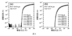
- Embodiment 6 is a view showing a device light response characteristic of a thin film transistor in Embodiment 6 of the present invention.
- FIG. 5 is a schematic structural view of a thin film transistor in Embodiment 7 of the present invention.
- Figure 6 is a schematic view showing the structure of a thin film transistor in Embodiment 8 of the present invention.
- the oxide semiconductor thin film is formed by doping a small amount of cerium oxide as a light stabilizer in an indium zinc oxide semiconductor film by a ceramic target magnetron sputtering method to form a cerium oxide doped oxidation.
- the Pr:IZO semiconductor film has a thickness of 20 nm and a carrier concentration of less than 5 ⁇ 10 19 cm -3 .
- Tb: The IGZO semiconductor film has a thickness of 40 nm and a carrier concentration of less than 5 ⁇ 10 19 cm -3 .
- An oxide semiconductor thin film of the present embodiment wherein the oxide semiconductor thin film is formed by doping a small amount of cerium oxide as a light stabilizer in an indium tin zinc-semiconductor thin film by an atomic layer deposition method to form yttrium oxide doped indium tin oxide.
- a zinc (Dy:ITZO) semiconductor thin film material in which Dy:In:Sn:Zn 0.11:1:1:1 mol.
- Dy: The thickness of the ITZO semiconductor film is 30 nm, and the carrier concentration is less than 5 ⁇ 10 19 cm -3 .
- the Yb:ZTO semiconductor film has a thickness of 30 nm and a carrier concentration of less than 5 ⁇ 10 19 cm -3 .
- a thin film transistor of the present embodiment is an etch barrier structure, and its structure is as shown in FIG. 1 , and is provided with a substrate 01 , a gate electrode 02 on the substrate 01 , and a substrate 01 and a gate electrode 02 .
- the insulating layer 03, the channel layer 04 covering the upper surface of the insulating layer 03 and corresponding to the gate electrode 02, the etch barrier layer 05, and the source electrode 06-1 which are spaced apart from each other and electrically connected to both ends of the channel layer 04 And drain 06-2, and passivation layer 07.
- the substrate 01 is a glass substrate covered with a buffer layer of silicon oxide.
- the material of the gate electrode 02 is a molybdenum aluminum molybdenum (Mo/Al/Mo) laminated structure prepared by metal magnetron sputtering, and has a thickness of 50/200/50 nm.
- the insulating layer 03 is a laminate of silicon nitride (Si 3 N 4 ) and silicon oxide (SiO 2 ) prepared by chemical vapor deposition, and has a thickness of 250/50 nm.
- the material of the channel layer 04 is yttria-doped indium zinc oxide (Pr:IZO) and yttria-doped indium gallium zinc oxide (Tb: IGZO) of Examples 1 and 2, respectively.
- the material of the etch barrier layer 05 and the passivation layer 07 is silicon oxide (SiO 2 ) prepared by chemical vapor deposition, and the thickness is 300 nm.
- the material of the source 06-1 and the drain 06-2 is a metal molybdenum aluminum molybdenum (Mo/Al/Mo) laminated structure having a thickness of 50/200/50 nm.
- the thin film transistor of this embodiment may be a closed structure including only a substrate, a gate, an insulating layer, a channel layer, an etch barrier layer, a source and a drain, and a passivation layer, and may further include a pixel defining layer and the like. Can be integrated with other devices.
- the patterning of the film is performed by photolithography and etching in combination with wet or dry etching.
- the photoreaction characteristics of the devices prepared by using the two channel layer materials Pr: IZO and Tb: IGZO in the present embodiment are respectively shown in (a) and (b) of FIG. 2 . It can be seen from Fig. 2 that by incorporating a certain amount of yttrium oxide or ytterbium oxide, the threshold voltage is hardly changed under the irradiation of different wavelengths of light and the dark condition (Dark), and excellent light is exhibited. stability.
- the experimental results show that the incorporation of a certain amount of rare earth oxide in the base oxide material of the present invention can effectively improve the light stability of the material.
- a thin film transistor of the present embodiment is a back channel etch type structure, and its structure is shown in FIG. 3, and is provided with a substrate 01, a gate electrode 02 located above the substrate 01, and a substrate 01 and a gate electrode 02.
- the upper insulating layer 03, the channel layer 04 covering the upper surface of the insulating layer 03 and corresponding to the gate electrode 02, and the source electrode 05-1 and the drain electrode 50 which are spaced apart from each other and electrically connected to both ends of the channel layer 04 -2, and passivation layer 06.
- the substrate 01 is a flexible polyimide (PI) substrate covered with a buffer layer of silicon oxide.
- the material of the gate electrode 02 is a molybdenum aluminum molybdenum (Mo/Al/Mo) laminated structure prepared by metal magnetron sputtering, and has a thickness of 50/200/50 nm.
- the insulating layer 03 is a laminate of silicon nitride (Si 3 N 4 ) and silicon oxide (SiO 2 ) prepared by chemical vapor deposition, and has a thickness of 250/50 nm.
- the material of the channel layer 04 is yttria-doped indium tin zinc oxide (Dy:ITZO) and yttria-doped zinc tin oxide (Yb:ZTO) of Examples 3 and 4, respectively.
- the material of source 05-1 and drain 05-2 is a metal molybdenum aluminum molybdenum (Mo/Al/Mo) laminated structure with a thickness of 50/200/50 nm, which is carried out using a commercial phosphoric acid molybdenum aluminum molybdenum etching solution. Patterned.
- the material of the passivation layer 06 is silicon oxide (SiO 2 ) prepared by chemical vapor deposition and has a thickness of 300 nm.
- the thin film transistor of this embodiment may be a closed structure including only a substrate, a gate, an insulating layer, a channel layer, a source and a drain, and a passivation layer, and may further include a pixel defining layer and the like, and may also be integrated with other devices. Wait.
- the patterning of the film is performed by photolithography and etching in combination with wet or dry etching.
- the photo response characteristics of the devices prepared by using the two channel layer materials Dy: ITZO and Yb: ZTO, respectively, in this embodiment are shown in (a) and (b) of FIG. 4, respectively. It can be seen from the results in Fig. 4 that by incorporating a certain amount of cerium oxide or cerium oxide, the threshold voltage is hardly changed with the incident light of different wavelengths and the dark condition (Dark), showing excellent performance. Light stability.
- the experimental results show that the incorporation of a certain amount of rare earth oxide in the base oxide material of the present invention can effectively improve the light stability of the material.
- a thin film transistor of the present embodiment is a back channel etch type structure, and a schematic structural view thereof is shown in FIG. 5, and is provided with a substrate 01, a gate electrode 02 located above the substrate 01, and a substrate 01 and a gate electrode 02.
- the substrate 01 is a flexible polyimide (PI) substrate covered with a buffer layer of silicon oxide.
- the material of the gate electrode 02 is a molybdenum aluminum molybdenum (Mo/Al/Mo) laminated structure prepared by metal magnetron sputtering, and has a thickness of 50/200/50 nm.
- the insulating layer 03 is a laminate of silicon nitride (Si 3 N 4 ) and silicon oxide (SiO 2 ) prepared by chemical vapor deposition, and has a thickness of 250/50 nm.
- the material of the channel layer 04 was yttria-doped indium zinc oxide (Pr: IZO) in Example 1, and the thickness was 20 nm.
- the material of the channel protective layer 05 is a tin oxide doped oxide or carbon film prepared by magnetron sputtering, and has a thickness of 10 nm.
- the material of source 06-1 and drain 06-2 is a metal molybdenum aluminum molybdenum (Mo/Al/Mo) laminated structure with a thickness of 50/200/50 nm, which is carried out using a commercial phosphoric acid molybdenum aluminum molybdenum etching solution. Patterned.
- the material of the passivation layer 07 is silicon oxide (SiO 2 ) prepared by chemical vapor deposition and has a thickness of 300 nm.
- the thin film transistor of this embodiment may be a closed structure including only a substrate, a gate, an insulating layer, a channel layer, a channel protective layer, a source and a drain, and a passivation layer, and may further include a pixel defining layer and the like. Can be integrated with other devices.
- the patterning of the film is performed by photolithography and etching in combination with wet or dry etching.
- the corresponding photo-response characteristics of the prepared device show that the threshold voltage is hardly changed with the incident light of different wavelengths, showing excellent light stability.
- a thin film transistor of the present embodiment is a self-aligned structure, and its structure is shown in FIG. 6.
- the substrate 01, the buffer layer 02, the channel layer 03, and the insulating layer above the channel layer 03 are provided. 04 and a gate electrode 05, a spacer layer 06 covering the upper surface of the channel layer 03, and a source electrode 07-1 and a drain electrode 07-2 which are spaced apart from each other and electrically connected to both ends of the channel layer.
- the substrate 01 is a hard glass substrate.
- the buffer layer 02 is a plasma enhanced chemical vapor deposition method for preparing silicon oxide.
- the material of the channel layer 03 was yttria-doped indium gallium zinc oxide (Tb: IGZO) in Example 2 and had a thickness of 40 nm.
- the gate insulating layer 04 is silicon oxide and has a thickness of 300 nm; the gate electrode 05 is a molybdenum aluminum molybdenum (Mo/Al/Mo) laminated structure prepared by magnetron sputtering, and has a thickness of 50/200/50 nm.
- Mo/Al/Mo molybdenum aluminum molybdenum
- the spacer layer 06 is silicon nitride and has a thickness of 200 nm.
- the material of the source 07-1 and the drain 07-2 is a metal molybdenum aluminum molybdenum (Mo/Al/Mo) laminated structure having a thickness of 50/200/50 nm.
- the thin film transistor of this embodiment may be a closed structure including only a substrate, a channel layer, an insulating layer, a gate, a spacer layer, a source and a drain, and may further include a passivation layer, a pixel defining layer, and the like. Integration with other devices, etc.
- the patterning of the film is performed by photolithography and etching in combination with wet or dry etching.
- the corresponding photo-response characteristics of the prepared device show that the threshold voltage is hardly changed with the incident light of different wavelengths, showing excellent light stability.
Landscapes
- Chemical & Material Sciences (AREA)
- Engineering & Computer Science (AREA)
- Ceramic Engineering (AREA)
- Manufacturing & Machinery (AREA)
- Organic Chemistry (AREA)
- Structural Engineering (AREA)
- Materials Engineering (AREA)
- Thin Film Transistor (AREA)
- Crystallography & Structural Chemistry (AREA)
- Optics & Photonics (AREA)
- Physics & Mathematics (AREA)
- Inorganic Chemistry (AREA)
- General Chemical & Material Sciences (AREA)
- Chemical Kinetics & Catalysis (AREA)
Abstract
一种氧化物半导体薄膜及由其制备的薄膜晶体管。该氧化物半导体薄膜由金属氧化物半导体薄膜中掺入少量稀土氧化物得到。该薄膜晶体管包括栅极(02)、氧化物半导体薄膜制备的沟道层(04)、位于栅极和沟道层之间的栅绝缘层、以及分别连接在沟道层两端的源极(06-1)和漏极(06-2)。该氧化物半导体薄膜材料及由其制备的薄膜晶体管具有优异的光照稳定性,而且制备工艺简单、适用性强。
Description
本发明属于半导体材料与器件技术领域,具体涉及一种氧化物半导体薄膜及由其制备的薄膜晶体管。
新型平板显示(FPD,Flat Panel Display)产业的核心技术是薄膜晶体管(TFT,Thin Film Transistor)背板技术。金属氧化物TFT(MO-TFT,Metal Oxide-TFT)不仅具有较高的迁移率(在1~100cm2/(V·s)左右),而且制作工艺相对简单,可以和目前的a-Si工艺兼容,制造成本较低,还具有优异的大面积均匀性。因此,MO-TFT技术自诞生以来便备受业界瞩目。
众所周知,作为显示器件核心部件的薄膜晶体管,在显示领域的应用中,其不可避免地会受到光的照射;而目前所开发的氧化物半导体薄膜由于氧空位的存在,使得禁带中产生相应的带隙态。该带隙态受到特定能量的光照射后,会激发出相应的电子空穴对,其在栅场的作用下导致器件阈值电压的偏移,从而引起显示画面的劣化。因此,如何实现优异的光照稳定性(在受到光照射时,器件的阈值电压几乎不发生偏移)是氧化物薄膜晶体管器件在实际应用中必须克服的难题。
现有技术,一方面,通过掺入一定量高断键能的氧化物,用以降低半导体薄膜中氧空位的浓度,这能一定程度上改善器件的光照稳定性,但同时也会降低器件的迁移率;而且,对于其在实际应用中而言,还存在巨大的挑战。另外一种方式,通过增加类似硅基工艺中的黑矩阵,对薄膜晶体管的有源层进行遮光处理。但是,该方式仅能一定程度上改善器件的光响应特性,对于长时间光
照条件下的稳定性改善有限,使其应用领域受到了严重的限制。而且,增加遮光工艺,也即增加了制备的复杂程度,造成制造成本的提高。因此,提高氧化物薄膜晶体管的光照稳定性具有非常重大的现实意义。
因此,开发一种具有优异的光照稳定性的氧化物半导体材料,对于氧化物薄膜晶体管的产业化应用具有非同寻常的意义。
发明内容
为了解决以上现有技术的缺点和不足之处,本发明的首要目的在于提供一种氧化物半导体薄膜。
本发明的另一目的在于提供一种由上述氧化物半导体薄膜作为沟道层材料制备的薄膜晶体管。
本发明目的通过以下技术方案实现:
一种氧化物半导体薄膜,所述氧化物半导体薄膜为:在金属氧化物(Metal Oxide,MO)半导体薄膜中掺入少量稀土氧化物(Rare-earth Oxides,RO)作为光稳定剂,形成(MO)x(RO)y半导体材料,其中0<x<1,0.0001≤y≤0.2,x+y=1。
所述金属氧化物MO中,M为In、Zn、Ga、Sn、Si、Al、Mg、Zr、Hf、Ta中的一种元素或两种以上的任意组合。
所述稀土氧化物RO材料包含:氧化镨、氧化铽、氧化镝、氧化镱中的一种或任意两种以上材料组合。
优选地,0.001≤y≤0.1;更优选为0.001≤y≤0.05。
优选地,所述氧化物半导体薄膜的厚度为5~100nm。
优选地,所述氧化物半导体薄膜的载流子浓度小于5×1019cm-3。
优选地,所述氧化物半导体薄膜采用单靶溅射的方法制备,或者采用溶液法、原子层沉积或脉冲激光沉积中的任意一种方式制备。
一种薄膜晶体管,所述薄膜晶体管包括栅极、沟道层、位于栅极和沟道层之间的栅绝缘层、以及分别连接在沟道层两端的源极和漏极;所述沟道层材料
为上述氧化物半导体薄膜。
相对于现有技术,本发明具有如下优点及有益效果:
(1)本发明的氧化物半导体薄膜及薄膜晶体管,具有优异的光照稳定性。这是因为稀土氧化物掺入金属氧化物半导体中,稀土金属原子替代了原金属原子而导致原来的M-M相互作用减弱,致使价带顶位移,使原金属氧化物半导体材料能带结构由直接带隙向间接带隙转变。在入射光照射时,价带电子需要与声子相互作用才能跃迁到导带,对输运特性产生贡献。因此,稀土金属氧化物的掺入可以大大减少薄膜晶体管工作时的光生载流子。也即,在入射光照射时,器件的阈值电压和未受光照时几乎不发生偏移,同时其他性能参数亦不受光照影响;
(2)本发明的氧化物半导体薄膜材料中,稀土金属氧化物的含量相对较少,其对基体材料(化合物中占主要成分的材料)的迁移率等性能影响较小,不会造成器件基本性能的退化;
(3)本发明的氧化物半导体薄膜材料具有非常优异的光照稳定性,而且具有制备工艺简单、适用性强的特点,其对不同体系基体材料的改善同样明显。
图1是本发明实施例5中薄膜晶体管的结构示意图;
图2是本发明实施例5中薄膜晶体管的器件光响应特性图;
图3是本发明实施例6中薄膜晶体管的结构示意图;
图4是本发明实施例6中薄膜晶体管的器件光响应特性图;
图5是本发明实施例7中薄膜晶体管的结构示意图;
图6是本发明实施例8中薄膜晶体管的结构示意图。
下面结合实施例及附图对本发明作进一步详细的描述,但本发明的实施方
式不限于此。
实施例1
本实施例的一种氧化物半导体薄膜,所述氧化物半导体薄膜为:通过陶瓷靶磁控溅射方式在氧化铟锌半导体薄膜中掺入少量氧化镨作为光稳定剂,形成氧化镨掺杂氧化铟锌(Pr:IZO)半导体薄膜材料,其中,Pr:In:Zn=0.2:5:1mol。Pr:IZO半导体薄膜的厚度为20nm,载流子浓度小于5×1019cm-3。
实施例2
本实施例的一种氧化物半导体薄膜,所述氧化物半导体薄膜为:通过陶瓷靶磁控溅射方式在氧化铟镓锌半导体薄膜中掺入少量氧化铽作为光稳定剂,形成氧化铽掺杂氧化铟镓锌(Tb:IGZO)半导体薄膜材料,其中,Tb:In:Ga:Zn=0.1:1:1:0.5mol。Tb:IGZO半导体薄膜的厚度为40nm,载流子浓度小于5×1019cm-3。
实施例3
本实施例的一种氧化物半导体薄膜,所述氧化物半导体薄膜为:通过原子层沉积法在氧化铟锡锌半导体薄膜中掺入少量氧化铥作为光稳定剂,形成氧化铥掺杂氧化铟锡锌(Dy:ITZO)半导体薄膜材料,其中,Dy:In:Sn:Zn=0.1:1:1:1mol。Dy:ITZO半导体薄膜的厚度为30nm,载流子浓度小于5×1019cm-3。
实施例4
本实施例的一种氧化物半导体薄膜,所述氧化物半导体薄膜为:通过原子层沉积法在氧化锌锡半导体薄膜中掺入少量氧化镱作为光稳定剂,形成氧化镱掺杂氧化锌锡(Yb:ZTO)半导体薄膜材料,其中,Yb:Sn:Zn=0.2:1:1mol。Yb:ZTO半导体薄膜的厚度为30nm,载流子浓度小于5×1019cm-3。
实施例5
本实施例的一种薄膜晶体管,为刻蚀阻挡型结构,其结构示意图如图1所示,设置有:基板01、位于基板01之上的栅极02、位于基板01和栅极02之上的绝缘层03、覆盖在绝缘层03上表面并与栅极02对应的沟道层04、刻蚀阻挡层05、相互间隔并与沟道层04的两端电性相连的源极06-1和漏极06-2、以及钝化层07。
基板01为玻璃衬底,其上覆盖有缓冲层氧化硅。
栅极02的材料为金属磁控溅射方式制备的钼铝钼(Mo/Al/Mo)叠层结构,厚度为50/200/50nm。
绝缘层03为化学气相沉积方式制备的氮化硅(Si3N4)和氧化硅(SiO2)的叠层,厚度为250/50nm。
沟道层04的材料分别为实施例1和实施例2的氧化镨掺杂氧化铟锌(Pr:IZO)和氧化铽掺杂氧化铟镓锌(Tb:IGZO)两种材料。
刻蚀阻挡层05和钝化层07的材料为化学气相沉积方式制备的氧化硅(SiO2),厚度都为300nm。
源极06-1以及漏极06-2的材料为金属钼铝钼(Mo/Al/Mo)叠层结构,厚度为50/200/50nm。
本实施例的薄膜晶体管可以为仅包括基板、栅极、绝缘层、沟道层、刻蚀阻挡层、源极和漏极、钝化层的封闭结构,也可以进一步包括像素定义层等,还可以与其它器件集成等。
其中薄膜的图案化采用光刻、并结合湿法或干法的刻蚀方式进行。
本实施例分别采用两种沟道层材料Pr:IZO和Tb:IGZO所制备的器件对应的光响应特性分别如图2中的(a)和(b)所示。由图2可以看出,通过掺入一定含量的氧化镨或氧化铥,器件随着不同波长的入射光照射及避光条件(Dark)下,阈值电压几乎不发生变化,表现出了优异的光稳定性。实验结果表明,本发明在基体氧化物材料中,掺入一定量的稀土氧化物能有效提高材料的光稳定性。
实施例6
本实施例的一种薄膜晶体管,为背沟道刻蚀型结构,其结构示意图如图3所示,设置有:基板01、位于基板01之上的栅极02、位于基板01和栅极02之上的绝缘层03、覆盖在绝缘层03上表面并与栅极02对应的沟道层04、相互间隔并与沟道层04的两端电性相连的源极05-1和漏极05-2、以及钝化层06。
基板01为柔性聚酰亚胺(PI)衬底,其上覆盖有缓冲层氧化硅。
栅极02的材料为金属磁控溅射方式制备的钼铝钼(Mo/Al/Mo)叠层结构,厚度为50/200/50nm。
绝缘层03为化学气相沉积方式制备的氮化硅(Si3N4)和氧化硅(SiO2)的叠层,厚度为250/50nm。
沟道层04的材料分别为实施例3和实施例4的氧化铥掺杂氧化铟锡锌(Dy:ITZO)和氧化镱掺杂氧化锌锡(Yb:ZTO)两种材料。
源极05-1以及漏极05-2的材料为金属钼铝钼(Mo/Al/Mo)叠层结构,厚度为50/200/50nm,其采用商用的磷酸基钼铝钼刻蚀液进行图案化。
钝化层06的材料为化学气相沉积方式制备的氧化硅(SiO2),厚度为300nm。
本实施例的薄膜晶体管可以为仅包括基板、栅极、绝缘层、沟道层、源极和漏极、钝化层的封闭结构,也可以进一步包括像素定义层等,还可以与其它器件集成等。
其中薄膜的图案化采用光刻、并结合湿法或干法的刻蚀方式进行。
本实施例分别采用两种沟道层材料Dy:ITZO和Yb:ZTO所制备的器件对应的光响应特性分别如图4中的(a)和(b)所示。由图4结果可以看出,通过掺入一定含量的氧化铥或氧化镱,器件随着不同波长的入射光照射及避光条件(Dark)下,阈值电压几乎不发生变化,表现出了优异的光稳定性。实验结果表明,本发明在基体氧化物材料中,掺入一定量的稀土氧化物能有效提高材料的光稳定性。
实施例7
本实施例的一种薄膜晶体管,为背沟道刻蚀型结构,其结构示意图如图5所示,设置有:基板01、位于基板01之上的栅极02、位于基板01和栅极02之上的绝缘层03、覆盖在绝缘层03上表面并与栅极02对应的沟道层04、沟道保护层05、相互间隔并与沟道层的两端电性相连的源极06-1和漏极06-2、以及钝化层07。
基板01为柔性聚酰亚胺(PI)衬底,其上覆盖有缓冲层氧化硅。
栅极02的材料为金属磁控溅射方式制备的钼铝钼(Mo/Al/Mo)叠层结构,厚度为50/200/50nm。
绝缘层03为化学气相沉积方式制备的氮化硅(Si3N4)和氧化硅(SiO2)的叠层,厚度为250/50nm。
沟道层04的材料为实施例1中的氧化镨掺杂氧化铟锌(Pr:IZO),厚度为20nm。
沟道保护层05的材料为磁控溅射方式制备的氧化锡掺杂氧化物或碳膜,厚度为10nm。
源极06-1以及漏极06-2的材料为金属钼铝钼(Mo/Al/Mo)叠层结构,厚度为50/200/50nm,其采用商用的磷酸基钼铝钼刻蚀液进行图案化。
钝化层07的材料为化学气相沉积方式制备的氧化硅(SiO2),厚度为300nm。
本实施例的薄膜晶体管可以为仅包括基板、栅极、绝缘层、沟道层、沟道保护层、源极和漏极、钝化层的封闭结构,也可以进一步包括像素定义层等,还可以与其它器件集成等。
其中薄膜的图案化采用光刻、并结合湿法或干法的刻蚀方式进行。
所制备的器件对应的光响应特性结果表明:器件随着不同波长的入射光照射,阈值电压几乎不发生变化,表现出了优异的光稳定性。
实施例8
本实施例的一种薄膜晶体管,为自对准型结构,其结构示意图如图6所示,设置有:基板01、缓冲层02、沟道层03、位于沟道层03之上的绝缘层04以及栅极05、覆盖在沟道层03上表面的间隔层06、相互间隔并与沟道层的两端电性相连的源极07-1和漏极07-2。
基板01为硬质玻璃衬底。
缓冲层02为等离子增强化学气相沉积方式制备氧化硅。
沟道层03的材料为实施例2中的氧化铽掺杂氧化铟镓锌(Tb:IGZO),厚度为40nm。
栅绝缘层04为氧化硅,厚度为300nm;栅极05为磁控溅射方式制备的钼铝钼(Mo/Al/Mo)叠层结构,厚度为50/200/50nm。
间隔层06为的氮化硅,厚度为200nm。
源极07-1以及漏极07-2的材料为金属钼铝钼(Mo/Al/Mo)叠层结构,厚度为50/200/50nm。
本实施例的薄膜晶体管可以为仅包括基板、沟道层、绝缘层、栅极、间隔层、源极和漏极的封闭结构,也可以进一步包括钝化层、以及像素定义层等,还可以与其它器件集成等。
其中薄膜的图案化采用光刻、并结合湿法或干法的刻蚀方式进行。
所制备的器件对应的光响应特性结果表明:器件随着不同波长的入射光照射,阈值电压几乎不发生变化,表现出了优异的光稳定性。
上述实施例为本发明较佳的实施方式,但本发明的实施方式并不受上述实施例的限制,其它的任何未背离本发明的精神实质与原理下所作的改变、修饰、替代、组合、简化,均应为等效的置换方式,都包含在本发明的保护范围之内。
Claims (9)
- 一种氧化物半导体薄膜,其特征在于所述氧化物半导体薄膜为:在金属氧化物MO半导体薄膜中掺入少量稀土氧化物RO作为光稳定剂,形成(MO)x(RO)y半导体材料,其中0<x<1,0.0001≤y≤0.2,x+y=1。
- 根据权利要求1所述的一种氧化物半导体薄膜,其特征在于:所述金属氧化物MO中,M为In、Zn、Ga、Sn、Si、Al、Mg、Zr、Hf、Ta中的一种元素或两种以上的任意组合。
- 根据权利要求1所述的一种氧化物半导体薄膜,其特征在于:所述稀土氧化物RO材料包含:氧化镨、氧化铽、氧化镝、氧化镱中的一种或任意两种以上材料组合。
- 根据权利要求1所述的一种氧化物半导体薄膜,其特征在于:0.001≤y≤0.1。
- 根据权利要求4所述的一种氧化物半导体薄膜,其特征在于:0.001≤y≤0.05。
- 根据权利要求1所述的一种氧化物半导体薄膜,其特征在于:所述氧化物半导体薄膜的厚度为5~100nm。
- 根据权利要求1所述的一种氧化物半导体薄膜,其特征在于:所述氧化物半导体薄膜的载流子浓度小于5×1019cm-3。
- 根据权利要求1所述的一种氧化物半导体薄膜,其特征在于:所述氧化物半导体薄膜采用单靶溅射的方法制备,或者采用溶液法、原子层沉积或脉冲激光沉积中的任意一种方式制备。
- 一种薄膜晶体管,所述薄膜晶体管包括栅极、沟道层、位于栅极和沟道层之间的栅绝缘层、以及分别连接在沟道层两端的源极和漏极;其特征在于:所述沟道层材料为权利要求1~8任一项所述的氧化物半导体薄膜。
Priority Applications (3)
| Application Number | Priority Date | Filing Date | Title |
|---|---|---|---|
| US16/529,833 US11677031B2 (en) | 2017-04-10 | 2019-08-02 | Oxide semiconductor thin-film and thin-film transistor consisted thereof |
| US17/105,655 US11545580B2 (en) | 2017-11-15 | 2020-11-27 | Metal oxide (MO semiconductor and thin-film transistor and application thereof |
| US17/994,022 US12520538B2 (en) | 2017-04-10 | 2022-11-25 | Rare-earth doped semiconductor material, thin-film transistor, and application |
Applications Claiming Priority (2)
| Application Number | Priority Date | Filing Date | Title |
|---|---|---|---|
| CN201710229199.9 | 2017-04-10 | ||
| CN201710229199.9A CN107146816B (zh) | 2017-04-10 | 2017-04-10 | 一种氧化物半导体薄膜及由其制备的薄膜晶体管 |
Related Child Applications (1)
| Application Number | Title | Priority Date | Filing Date |
|---|---|---|---|
| US16/529,833 Continuation US11677031B2 (en) | 2017-04-10 | 2019-08-02 | Oxide semiconductor thin-film and thin-film transistor consisted thereof |
Publications (1)
| Publication Number | Publication Date |
|---|---|
| WO2018188332A1 true WO2018188332A1 (zh) | 2018-10-18 |
Family
ID=59774618
Family Applications (1)
| Application Number | Title | Priority Date | Filing Date |
|---|---|---|---|
| PCT/CN2017/111109 Ceased WO2018188332A1 (zh) | 2017-04-10 | 2017-11-15 | 一种氧化物半导体薄膜及由其制备的薄膜晶体管 |
Country Status (3)
| Country | Link |
|---|---|
| US (1) | US11677031B2 (zh) |
| CN (1) | CN107146816B (zh) |
| WO (1) | WO2018188332A1 (zh) |
Cited By (1)
| Publication number | Priority date | Publication date | Assignee | Title |
|---|---|---|---|---|
| US20210083125A1 (en) * | 2019-09-18 | 2021-03-18 | South China University Of Technology | Composite metal oxide semiconductor and thin-film transistor made therefrom and its application |
Families Citing this family (16)
| Publication number | Priority date | Publication date | Assignee | Title |
|---|---|---|---|---|
| CN112582466B (zh) * | 2020-11-20 | 2025-07-01 | 华南理工大学 | 一种金属氧化物半导体及薄膜晶体管与应用 |
| CN107146816B (zh) | 2017-04-10 | 2020-05-15 | 华南理工大学 | 一种氧化物半导体薄膜及由其制备的薄膜晶体管 |
| CN108735821B (zh) * | 2018-05-29 | 2021-06-08 | 华南理工大学 | 一种镨铟锌氧化物薄膜晶体管及其制备方法 |
| CN108987470B (zh) * | 2018-07-16 | 2021-01-01 | 华南理工大学 | 薄膜晶体管、显示面板及薄膜晶体管的制作方法 |
| CN110008936A (zh) * | 2019-04-19 | 2019-07-12 | 广州新视界光电科技有限公司 | 一种指纹识别模组和指纹识别设备 |
| CN110797395A (zh) * | 2019-09-18 | 2020-02-14 | 华南理工大学 | 掺杂型金属氧化物半导体及薄膜晶体管与应用 |
| CN113838801B (zh) | 2020-06-24 | 2024-10-22 | 京东方科技集团股份有限公司 | 半导体基板的制造方法和半导体基板 |
| CN114649408B (zh) * | 2020-12-18 | 2025-10-17 | 京东方科技集团股份有限公司 | 金属氧化物半导体材料、靶材及其制备方法、薄膜晶体管及其制备方法 |
| EP4141959A4 (en) * | 2021-01-28 | 2023-08-09 | BOE Technology Group Co., Ltd. | THIN-FILM TRANSISTOR AND METHOD FOR MAKING IT, MATRIX SUBSTRATE AND DISPLAY DEVICE |
| CN113066599B (zh) * | 2021-02-03 | 2024-12-13 | 华南理工大学 | 一种金属氧化物透明导电薄膜及其应用 |
| CN115084275B (zh) * | 2021-03-15 | 2024-09-27 | 京东方科技集团股份有限公司 | 金属氧化物TFT及制造方法、x射线探测器和显示面板 |
| CN113078042B (zh) * | 2021-03-22 | 2022-04-26 | 青岛科技大学 | 一种薄膜晶体管制备方法 |
| CN116207137B (zh) * | 2022-11-24 | 2025-11-07 | 漳州市合琦靶材科技有限公司 | 一种高迁移率铟镓锌铽氧基复合薄膜晶体管及其制备方法 |
| CN116813310B (zh) * | 2023-06-01 | 2024-06-07 | 先导薄膜材料(广东)有限公司 | 一种稀土元素掺杂氧化铟锡镓靶材及其制备方法 |
| CN117457753B (zh) * | 2023-11-20 | 2024-11-19 | 漳州市合琦靶材科技有限公司 | 一种双有源层铽掺杂氧化物薄膜晶体管及其制备方法 |
| CN119569421A (zh) * | 2024-11-04 | 2025-03-07 | 广州市尤特新材料有限公司 | 一种aitzo靶材及其制备方法与在制备太阳能电池中的应用 |
Citations (2)
| Publication number | Priority date | Publication date | Assignee | Title |
|---|---|---|---|---|
| CN102832235A (zh) * | 2012-09-14 | 2012-12-19 | 华南理工大学 | 氧化物半导体及其制造方法 |
| CN107146816A (zh) * | 2017-04-10 | 2017-09-08 | 华南理工大学 | 一种氧化物半导体薄膜及由其制备的薄膜晶体管 |
Family Cites Families (49)
| Publication number | Priority date | Publication date | Assignee | Title |
|---|---|---|---|---|
| US5686557A (en) * | 1994-09-21 | 1997-11-11 | Tomoegawa Paper Co., Ltd. | Polyamide resin which can be dissolved in alcohol solvent, composition thereof, and method of use thereof |
| US5820960A (en) * | 1996-05-15 | 1998-10-13 | Saint-Gobain/Norton Industrial Ceramics Corporation | Thin zirconia disk substrate |
| JP2002080693A (ja) * | 2000-06-28 | 2002-03-19 | Nippon Kayaku Co Ltd | エポキシ樹脂組成物及びその硬化物 |
| US6794031B2 (en) * | 2001-09-28 | 2004-09-21 | Ube Industries, Ltd. | Cover-lay film and printed circuit board having the same |
| US7544967B2 (en) * | 2005-03-28 | 2009-06-09 | Massachusetts Institute Of Technology | Low voltage flexible organic/transparent transistor for selective gas sensing, photodetecting and CMOS device applications |
| EP3614442A3 (en) * | 2005-09-29 | 2020-03-25 | Semiconductor Energy Laboratory Co., Ltd. | Semiconductor device having oxide semiconductor layer and manufactoring method thereof |
| US7993560B2 (en) * | 2006-04-20 | 2011-08-09 | Curwood, Inc. | Process for introducing an additive into a polymer melt |
| JP5279312B2 (ja) * | 2008-03-28 | 2013-09-04 | 株式会社東芝 | 半導体装置、及び半導体装置の製造方法 |
| KR101468591B1 (ko) * | 2008-05-29 | 2014-12-04 | 삼성전자주식회사 | 산화물 반도체 및 이를 포함하는 박막 트랜지스터 |
| US9666719B2 (en) * | 2008-07-31 | 2017-05-30 | Semiconductor Energy Laboratory Co., Ltd. | Semiconductor device and manufacturing method thereof |
| JP5451280B2 (ja) * | 2008-10-09 | 2014-03-26 | キヤノン株式会社 | ウルツ鉱型結晶成長用基板およびその製造方法ならびに半導体装置 |
| CN101740570B (zh) * | 2008-11-26 | 2011-06-15 | 中国科学院微电子研究所 | 互补型金属氧化物半导体晶体管器件及其制作方法 |
| CN101599436A (zh) * | 2009-07-03 | 2009-12-09 | 中国科学院微电子研究所 | 用于mos器件的金属栅极结构及其制作方法 |
| US8513720B2 (en) * | 2010-07-14 | 2013-08-20 | Sharp Laboratories Of America, Inc. | Metal oxide semiconductor thin film transistors |
| US8883555B2 (en) * | 2010-08-25 | 2014-11-11 | Semiconductor Energy Laboratory Co., Ltd. | Electronic device, manufacturing method of electronic device, and sputtering target |
| US9546416B2 (en) * | 2010-09-13 | 2017-01-17 | Semiconductor Energy Laboratory Co., Ltd. | Method of forming crystalline oxide semiconductor film |
| CN102446969B (zh) * | 2010-10-13 | 2015-03-18 | 中国科学院微电子研究所 | 半导体器件及其形成方法 |
| CN102464864A (zh) * | 2010-10-29 | 2012-05-23 | E.I.内穆尔杜邦公司 | 光稳定的共聚醚酯组合物 |
| TWI555205B (zh) * | 2010-11-05 | 2016-10-21 | 半導體能源研究所股份有限公司 | 半導體裝置及半導體裝置的製造方法 |
| US9443984B2 (en) * | 2010-12-28 | 2016-09-13 | Semiconductor Energy Laboratory Co., Ltd. | Semiconductor device and manufacturing method thereof |
| JP5977523B2 (ja) * | 2011-01-12 | 2016-08-24 | 株式会社半導体エネルギー研究所 | トランジスタの作製方法 |
| US8916867B2 (en) * | 2011-01-20 | 2014-12-23 | Semiconductor Energy Laboratory Co., Ltd. | Oxide semiconductor element and semiconductor device |
| US9397222B2 (en) * | 2011-05-13 | 2016-07-19 | Semiconductor Energy Laboratory Co., Ltd. | Display device and electronic device |
| JP6005401B2 (ja) * | 2011-06-10 | 2016-10-12 | 株式会社半導体エネルギー研究所 | 半導体装置の作製方法 |
| US8952377B2 (en) * | 2011-07-08 | 2015-02-10 | Semiconductor Energy Laboratory Co., Ltd. | Semiconductor device and manufacturing method thereof |
| US8952379B2 (en) * | 2011-09-16 | 2015-02-10 | Semiconductor Energy Laboratory Co., Ltd. | Semiconductor device |
| JP6226518B2 (ja) * | 2011-10-24 | 2017-11-08 | 株式会社半導体エネルギー研究所 | 半導体装置 |
| KR20130046357A (ko) * | 2011-10-27 | 2013-05-07 | 가부시키가이샤 한도오따이 에네루기 켄큐쇼 | 반도체 장치 |
| KR20130055521A (ko) * | 2011-11-18 | 2013-05-28 | 가부시키가이샤 한도오따이 에네루기 켄큐쇼 | 반도체 소자, 및 반도체 소자의 제작 방법, 및 반도체 소자를 포함하는 반도체 장치 |
| US8969130B2 (en) * | 2011-11-18 | 2015-03-03 | Semiconductor Energy Laboratory Co., Ltd. | Insulating film, formation method thereof, semiconductor device, and manufacturing method thereof |
| KR102072244B1 (ko) * | 2011-11-30 | 2020-01-31 | 가부시키가이샤 한도오따이 에네루기 켄큐쇼 | 반도체 장치 및 반도체 장치의 제작 방법 |
| KR102034911B1 (ko) * | 2012-01-25 | 2019-10-21 | 가부시키가이샤 한도오따이 에네루기 켄큐쇼 | 반도체 장치 및 반도체 장치의 제작 방법 |
| WO2013179922A1 (en) * | 2012-05-31 | 2013-12-05 | Semiconductor Energy Laboratory Co., Ltd. | Semiconductor device and method for manufacturing the same |
| US9153699B2 (en) * | 2012-06-15 | 2015-10-06 | Semiconductor Energy Laboratory Co., Ltd. | Thin film transistor with multiple oxide semiconductor layers |
| JP6224931B2 (ja) * | 2012-07-27 | 2017-11-01 | 株式会社半導体エネルギー研究所 | 半導体装置 |
| SG11201505225TA (en) * | 2012-08-03 | 2015-08-28 | Semiconductor Energy Lab | Oxide semiconductor stacked film and semiconductor device |
| TWI657539B (zh) * | 2012-08-31 | 2019-04-21 | Semiconductor Energy Laboratory Co., Ltd. | 半導體裝置 |
| TWI605593B (zh) * | 2012-11-15 | 2017-11-11 | 半導體能源研究所股份有限公司 | 半導體裝置 |
| US9905585B2 (en) * | 2012-12-25 | 2018-02-27 | Semiconductor Energy Laboratory Co., Ltd. | Semiconductor device comprising capacitor |
| KR102241249B1 (ko) * | 2012-12-25 | 2021-04-15 | 가부시키가이샤 한도오따이 에네루기 켄큐쇼 | 저항 소자, 표시 장치, 및 전자기기 |
| TWI620324B (zh) * | 2013-04-12 | 2018-04-01 | Semiconductor Energy Laboratory Co., Ltd. | 半導體裝置 |
| WO2014181777A1 (ja) * | 2013-05-09 | 2014-11-13 | 独立行政法人物質・材料研究機構 | 薄膜トランジスタおよびその製造方法 |
| US9704894B2 (en) * | 2013-05-10 | 2017-07-11 | Semiconductor Energy Laboratory Co., Ltd. | Display device including pixel electrode including oxide |
| US9006736B2 (en) * | 2013-07-12 | 2015-04-14 | Semiconductor Energy Laboratory Co., Ltd. | Semiconductor device |
| US9929279B2 (en) * | 2014-02-05 | 2018-03-27 | Semiconductor Energy Laboratory Co., Ltd. | Semiconductor device and manufacturing method thereof |
| CN104218074A (zh) * | 2014-09-16 | 2014-12-17 | 北京大学 | 一种非晶半导体薄膜及其制备方法和应用 |
| CN105472791A (zh) * | 2015-12-23 | 2016-04-06 | 东莞珂洛赫慕电子材料科技有限公司 | 一种稀土掺杂半导体红外辐射厚膜电子浆料及其制备方法 |
| US20160315163A1 (en) * | 2016-06-30 | 2016-10-27 | L'air Liquide, Societe Anonyme Pour L'etude Et L'exploitation Des Procedes Georges Claude | Process for forming gate insulators for tft structures |
| US11545581B2 (en) * | 2019-08-02 | 2023-01-03 | South China University Of Technology | Metal oxide (MO) semiconductor and thin-film transistor and application thereof |
-
2017
- 2017-04-10 CN CN201710229199.9A patent/CN107146816B/zh active Active
- 2017-11-15 WO PCT/CN2017/111109 patent/WO2018188332A1/zh not_active Ceased
-
2019
- 2019-08-02 US US16/529,833 patent/US11677031B2/en active Active
Patent Citations (2)
| Publication number | Priority date | Publication date | Assignee | Title |
|---|---|---|---|---|
| CN102832235A (zh) * | 2012-09-14 | 2012-12-19 | 华南理工大学 | 氧化物半导体及其制造方法 |
| CN107146816A (zh) * | 2017-04-10 | 2017-09-08 | 华南理工大学 | 一种氧化物半导体薄膜及由其制备的薄膜晶体管 |
Cited By (2)
| Publication number | Priority date | Publication date | Assignee | Title |
|---|---|---|---|---|
| US20210083125A1 (en) * | 2019-09-18 | 2021-03-18 | South China University Of Technology | Composite metal oxide semiconductor and thin-film transistor made therefrom and its application |
| US11984510B2 (en) * | 2019-09-18 | 2024-05-14 | South China University Of Technology | Composite metal oxide semiconductor and thin-film transistor made therefrom and its application |
Also Published As
| Publication number | Publication date |
|---|---|
| US20200027993A1 (en) | 2020-01-23 |
| CN107146816B (zh) | 2020-05-15 |
| US11677031B2 (en) | 2023-06-13 |
| CN107146816A (zh) | 2017-09-08 |
Similar Documents
| Publication | Publication Date | Title |
|---|---|---|
| CN107146816B (zh) | 一种氧化物半导体薄膜及由其制备的薄膜晶体管 | |
| TWI401804B (zh) | 薄膜電晶體及其製造方法 | |
| JP2022518522A (ja) | 複合金属酸化物半導体および薄膜トランジスタとその応用 | |
| JP2022518521A (ja) | ドーピングされた金属酸化物半導体および薄膜トランジスタとその応用 | |
| CN102082170B (zh) | 非晶态氧化物半导体材料、场效应晶体管和显示装置 | |
| CN104882486B (zh) | 高迁移率、高稳定性金属氧化物薄膜晶体管及其制备工艺 | |
| CN112582466B (zh) | 一种金属氧化物半导体及薄膜晶体管与应用 | |
| CN102084486A (zh) | 薄膜晶体管及显示装置 | |
| TW200937534A (en) | Method for manufacturing field-effect transistor | |
| US11037958B2 (en) | Array substrate and manufacturing method thereof | |
| JP2011071476A (ja) | 薄膜トランジスタ、薄膜トランジスタを用いた表示装置及び薄膜トランジスタの製造方法 | |
| CN106876327A (zh) | 一种阵列基板及其制备方法、显示装置 | |
| CN103545221B (zh) | 金属氧化物薄膜晶体管及其制备方法 | |
| JP5437776B2 (ja) | 酸化物半導体を用いた薄膜トランジスタおよびその製造方法 | |
| WO2022062454A1 (zh) | 一种金属氧化物半导体及薄膜晶体管与应用 | |
| CN114175271A (zh) | 薄膜晶体管、半导体基板和x射线平板探测器 | |
| WO2023141967A1 (zh) | 氧化物半导体靶材、薄膜、薄膜晶体管及提高其稳定性的方法 | |
| CN111697006A (zh) | 显示面板及显示面板的制备方法 | |
| US9070779B2 (en) | Metal oxide TFT with improved temperature stability | |
| JP2011258804A (ja) | 電界効果型トランジスタ及びその製造方法 | |
| CN115799276A (zh) | 驱动基板及显示面板 | |
| CN110444644A (zh) | 一种增强硅基铒掺杂ZnO薄膜电致发光的器件及制备方法 | |
| CN119947196A (zh) | 薄膜晶体管、显示面板及显示装置 | |
| CN104900707A (zh) | 双有源层结构氧化锌基薄膜晶体管及其制备方法 | |
| CN109638082B (zh) | 薄膜晶体管以及制备方法 |
Legal Events
| Date | Code | Title | Description |
|---|---|---|---|
| 121 | Ep: the epo has been informed by wipo that ep was designated in this application |
Ref document number: 17905166 Country of ref document: EP Kind code of ref document: A1 |
|
| NENP | Non-entry into the national phase |
Ref country code: DE |
|
| 32PN | Ep: public notification in the ep bulletin as address of the adressee cannot be established |
Free format text: NOTING OF LOSS OF RIGHTS PURSUANT TO RULE 112(1) EPC (EPO FORM 1205A DATED 27.01.2020) |
|
| 122 | Ep: pct application non-entry in european phase |
Ref document number: 17905166 Country of ref document: EP Kind code of ref document: A1 |