WO2018124055A1 - 撮像装置、カメラ、及び撮像方法 - Google Patents
撮像装置、カメラ、及び撮像方法 Download PDFInfo
- Publication number
- WO2018124055A1 WO2018124055A1 PCT/JP2017/046599 JP2017046599W WO2018124055A1 WO 2018124055 A1 WO2018124055 A1 WO 2018124055A1 JP 2017046599 W JP2017046599 W JP 2017046599W WO 2018124055 A1 WO2018124055 A1 WO 2018124055A1
- Authority
- WO
- WIPO (PCT)
- Prior art keywords
- frame image
- image
- pixel
- period
- light
- Prior art date
Links
- 238000003384 imaging method Methods 0.000 title claims abstract description 200
- 238000012937 correction Methods 0.000 claims abstract description 285
- 238000006243 chemical reaction Methods 0.000 claims abstract description 106
- 230000000694 effects Effects 0.000 claims abstract description 31
- 238000012935 Averaging Methods 0.000 claims description 13
- 239000010409 thin film Substances 0.000 claims description 7
- 230000005622 photoelectricity Effects 0.000 claims 1
- 238000000034 method Methods 0.000 description 124
- 230000008569 process Effects 0.000 description 120
- 238000007792 addition Methods 0.000 description 53
- 230000004048 modification Effects 0.000 description 49
- 238000012986 modification Methods 0.000 description 49
- 238000012545 processing Methods 0.000 description 48
- 238000010586 diagram Methods 0.000 description 28
- 238000009825 accumulation Methods 0.000 description 26
- 230000006870 function Effects 0.000 description 22
- 230000003287 optical effect Effects 0.000 description 11
- 230000003111 delayed effect Effects 0.000 description 9
- 238000010606 normalization Methods 0.000 description 9
- 235000019557 luminance Nutrition 0.000 description 8
- 230000003321 amplification Effects 0.000 description 6
- 238000005516 engineering process Methods 0.000 description 6
- 238000003199 nucleic acid amplification method Methods 0.000 description 6
- 238000004364 calculation method Methods 0.000 description 4
- 239000000470 constituent Substances 0.000 description 3
- 230000010354 integration Effects 0.000 description 3
- 239000004065 semiconductor Substances 0.000 description 3
- 230000006835 compression Effects 0.000 description 1
- 238000007906 compression Methods 0.000 description 1
- 238000004519 manufacturing process Methods 0.000 description 1
- 239000000463 material Substances 0.000 description 1
- 230000009467 reduction Effects 0.000 description 1
- 230000004044 response Effects 0.000 description 1
- 239000013589 supplement Substances 0.000 description 1
Images


Classifications
-
- H—ELECTRICITY
- H01—ELECTRIC ELEMENTS
- H01L—SEMICONDUCTOR DEVICES NOT COVERED BY CLASS H10
- H01L27/00—Devices consisting of a plurality of semiconductor or other solid-state components formed in or on a common substrate
- H01L27/14—Devices consisting of a plurality of semiconductor or other solid-state components formed in or on a common substrate including semiconductor components sensitive to infrared radiation, light, electromagnetic radiation of shorter wavelength or corpuscular radiation and specially adapted either for the conversion of the energy of such radiation into electrical energy or for the control of electrical energy by such radiation
- H01L27/144—Devices controlled by radiation
- H01L27/146—Imager structures
- H01L27/14601—Structural or functional details thereof
- H01L27/14638—Structures specially adapted for transferring the charges across the imager perpendicular to the imaging plane
-
- H—ELECTRICITY
- H04—ELECTRIC COMMUNICATION TECHNIQUE
- H04N—PICTORIAL COMMUNICATION, e.g. TELEVISION
- H04N25/00—Circuitry of solid-state image sensors [SSIS]; Control thereof
- H04N25/60—Noise processing, e.g. detecting, correcting, reducing or removing noise
- H04N25/63—Noise processing, e.g. detecting, correcting, reducing or removing noise applied to dark current
-
- H—ELECTRICITY
- H01—ELECTRIC ELEMENTS
- H01L—SEMICONDUCTOR DEVICES NOT COVERED BY CLASS H10
- H01L27/00—Devices consisting of a plurality of semiconductor or other solid-state components formed in or on a common substrate
- H01L27/02—Devices consisting of a plurality of semiconductor or other solid-state components formed in or on a common substrate including semiconductor components specially adapted for rectifying, oscillating, amplifying or switching and having potential barriers; including integrated passive circuit elements having potential barriers
- H01L27/04—Devices consisting of a plurality of semiconductor or other solid-state components formed in or on a common substrate including semiconductor components specially adapted for rectifying, oscillating, amplifying or switching and having potential barriers; including integrated passive circuit elements having potential barriers the substrate being a semiconductor body
- H01L27/10—Devices consisting of a plurality of semiconductor or other solid-state components formed in or on a common substrate including semiconductor components specially adapted for rectifying, oscillating, amplifying or switching and having potential barriers; including integrated passive circuit elements having potential barriers the substrate being a semiconductor body including a plurality of individual components in a repetitive configuration
- H01L27/118—Masterslice integrated circuits
- H01L27/11803—Masterslice integrated circuits using field effect technology
- H01L27/11807—CMOS gate arrays
-
- H—ELECTRICITY
- H01—ELECTRIC ELEMENTS
- H01L—SEMICONDUCTOR DEVICES NOT COVERED BY CLASS H10
- H01L27/00—Devices consisting of a plurality of semiconductor or other solid-state components formed in or on a common substrate
- H01L27/14—Devices consisting of a plurality of semiconductor or other solid-state components formed in or on a common substrate including semiconductor components sensitive to infrared radiation, light, electromagnetic radiation of shorter wavelength or corpuscular radiation and specially adapted either for the conversion of the energy of such radiation into electrical energy or for the control of electrical energy by such radiation
- H01L27/142—Energy conversion devices
-
- H—ELECTRICITY
- H04—ELECTRIC COMMUNICATION TECHNIQUE
- H04N—PICTORIAL COMMUNICATION, e.g. TELEVISION
- H04N23/00—Cameras or camera modules comprising electronic image sensors; Control thereof
- H04N23/50—Constructional details
- H04N23/55—Optical parts specially adapted for electronic image sensors; Mounting thereof
-
- H—ELECTRICITY
- H04—ELECTRIC COMMUNICATION TECHNIQUE
- H04N—PICTORIAL COMMUNICATION, e.g. TELEVISION
- H04N25/00—Circuitry of solid-state image sensors [SSIS]; Control thereof
- H04N25/40—Extracting pixel data from image sensors by controlling scanning circuits, e.g. by modifying the number of pixels sampled or to be sampled
-
- H—ELECTRICITY
- H04—ELECTRIC COMMUNICATION TECHNIQUE
- H04N—PICTORIAL COMMUNICATION, e.g. TELEVISION
- H04N25/00—Circuitry of solid-state image sensors [SSIS]; Control thereof
- H04N25/70—SSIS architectures; Circuits associated therewith
- H04N25/76—Addressed sensors, e.g. MOS or CMOS sensors
-
- H—ELECTRICITY
- H01—ELECTRIC ELEMENTS
- H01L—SEMICONDUCTOR DEVICES NOT COVERED BY CLASS H10
- H01L27/00—Devices consisting of a plurality of semiconductor or other solid-state components formed in or on a common substrate
- H01L27/14—Devices consisting of a plurality of semiconductor or other solid-state components formed in or on a common substrate including semiconductor components sensitive to infrared radiation, light, electromagnetic radiation of shorter wavelength or corpuscular radiation and specially adapted either for the conversion of the energy of such radiation into electrical energy or for the control of electrical energy by such radiation
- H01L27/144—Devices controlled by radiation
- H01L27/146—Imager structures
-
- Y—GENERAL TAGGING OF NEW TECHNOLOGICAL DEVELOPMENTS; GENERAL TAGGING OF CROSS-SECTIONAL TECHNOLOGIES SPANNING OVER SEVERAL SECTIONS OF THE IPC; TECHNICAL SUBJECTS COVERED BY FORMER USPC CROSS-REFERENCE ART COLLECTIONS [XRACs] AND DIGESTS
- Y02—TECHNOLOGIES OR APPLICATIONS FOR MITIGATION OR ADAPTATION AGAINST CLIMATE CHANGE
- Y02E—REDUCTION OF GREENHOUSE GAS [GHG] EMISSIONS, RELATED TO ENERGY GENERATION, TRANSMISSION OR DISTRIBUTION
- Y02E10/00—Energy generation through renewable energy sources
- Y02E10/50—Photovoltaic [PV] energy
Definitions
- the present invention relates to an imaging apparatus, a camera, and an imaging method for imaging an image.
- Patent Document 1 discloses that a dark current signal component in a light-shielded state is acquired and stored in a light-shielded state by narrowing the lens aperture, and a dark current included in a captured frame image using the stored dark current signal component.
- An imaging device that corrects to reduce signal components is described.
- this imaging apparatus in order to capture a continuous frame, it is necessary to open the lens aperture during the imaging period.
- this imaging apparatus in order to acquire the dark current signal component in the light shielding state, it is necessary to reduce the lens aperture for a certain period to be in the light shielding state. In other words, this imaging apparatus cannot acquire the dark current signal component in the light-shielded state during the imaging period of continuous frame images.
- the dark current signal component included in the frame image captured during the imaging period is calculated. It cannot be corrected to reduce.
- the present disclosure reduces the dark current signal component included in the frame image captured during the imaging period based on the dark current signal component in the light shielding state acquired during the imaging period of consecutive frame images. It is an object to provide an imaging apparatus, a camera, and an imaging method that can be corrected as described above.
- An imaging device generates charges due to an internal photoelectric effect by receiving light in a state where a voltage in a first predetermined range is applied, and receives light in a state where a voltage in a second predetermined range is applied.
- it includes a photoelectric conversion member that does not generate charges due to the internal photoelectric effect, and a plurality of pixel circuits that store charges generated by the photoelectric conversion members in units of pixels, and the amount of charges stored in the plurality of pixel circuits
- An image sensor that outputs a frame image based on the voltage, a voltage control unit that controls a voltage applied to the photoelectric conversion member, and at least a part of one or more frame images output from the image sensor.
- a correction unit that corrects the current signal component to be reduced, and the voltage control unit applies the first predetermined range to the photoelectric conversion member during a partial exposure period of a predetermined frame period.
- the voltage is applied, and the control is performed so that the voltage within the second predetermined range is applied to the photoelectric conversion member during a light shielding period other than the exposure period in the frame period, For each frame period, a signal frame image based on the amount of charge accumulated in the plurality of pixel circuits in the exposure period and a light shielding frame image based on the amount of charge accumulated in the plurality of pixel circuits in the light shielding period.
- the correction unit performs the correction on the signal frame image output from the image sensor using the light-shielded frame image output from the image sensor.
- a camera includes the imaging device and a lens that collects external light on the imaging device.
- An imaging method is an imaging method performed by an imaging device including an imaging element, a voltage control unit, and a correction unit, and the imaging element is in a state where a voltage in a first predetermined range is applied.
- a photoelectric conversion member that generates charges due to the internal photoelectric effect by receiving light, and that does not generate charges due to the internal photoelectric effect even when receiving light in a state where a voltage in the second predetermined range is applied, and the photoelectric conversion member A plurality of pixel circuits for accumulating charges in units of pixels, the imaging element outputting a frame image based on the amount of charges accumulated in the plurality of pixel circuits, and the voltage control unit includes the photoelectric conversion A voltage control step for controlling a voltage applied to the member; and the correction unit applies a dark current signal to at least a part of one or more frame images output from the image sensor.
- a correction step of correcting so as to reduce a component In the voltage control step, the voltage control unit applies the first predetermined range to the photoelectric conversion member during a partial exposure period of a predetermined frame period. The control is performed so that the voltage of the second predetermined range is applied to the photoelectric conversion member in a light shielding period other than the exposure period in the frame period, and in the imaging step, The image sensor is based on the signal frame image based on the amount of charge accumulated in the plurality of pixel circuits in the exposure period and the amount of charge accumulated in the plurality of pixel circuits in the light shielding period for each frame period.
- a shading frame image is output, and in the correction step, the correction unit outputs the signal frame image output from the image sensor from the image sensor. Using a light-blocking frame image, it performs the correction.
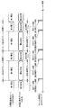
- FIG. 1 is a block diagram illustrating a configuration of a camera according to an embodiment.
- FIG. 2 is a block diagram showing the configuration of the image sensor.
- FIG. 3A is a plan view of the photoelectric conversion element.
- FIG. 3B is a side view of the photoelectric conversion element.
- FIG. 4 is a block diagram showing the configuration of the pixel circuit.
- FIG. 5A is a timing chart showing the operation of the voltage control unit.
- FIG. 5B is a timing chart showing the operation of the image sensor.
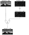
- FIG. 6 is a schematic diagram illustrating how correction is performed by the correction unit.
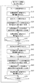
- FIG. 7 is a flowchart of the first frame image output process.
- FIG. 8 is a flowchart of the first correction process.
- FIG. 7 is a flowchart of the first frame image output process.
- FIG. 9 is a block diagram illustrating a configuration of a camera according to the first modification.
- FIG. 10A is a timing chart illustrating the operation of the voltage control unit.
- FIG. 10B is a timing chart illustrating the operation of the image sensor.
- FIG. 11 is a schematic diagram illustrating how correction is performed by the correction unit.
- FIG. 12 is a flowchart of the second frame image output process.
- FIG. 13 is a flowchart of the second correction process.
- FIG. 14 is a block diagram illustrating a configuration of an imaging apparatus according to the second modification.
- FIG. 15 is a schematic diagram illustrating a state of generation of the added light-shielded frame image performed by the added image generation unit.
- FIG. 16 is a schematic diagram illustrating how correction is performed by the correction unit.
- FIG. 10A is a timing chart illustrating the operation of the voltage control unit.
- FIG. 10B is a timing chart illustrating the operation of the image sensor.
- FIG. 11 is a schematic diagram
- FIG. 17 is a flowchart of the third correction process.
- FIG. 18 is a block diagram illustrating a configuration of a camera according to Modification 3.
- FIG. 19 is a schematic diagram illustrating a state of generation of an addition average shading frame image performed by the addition average image generation unit.
- FIG. 20 is a schematic diagram illustrating how correction is performed by the correction unit.
- FIG. 21 is a flowchart of the fourth correction process.
- FIG. 22 is a block diagram illustrating a configuration of a camera according to the fourth modification.
- FIG. 23A is a timing chart illustrating the operation of the voltage control unit.
- FIG. 23B is a timing chart illustrating the operation of the image sensor.
- FIG. 24 is a schematic diagram illustrating how correction is performed by the correction unit.
- FIG. 24 is a schematic diagram illustrating how correction is performed by the correction unit.
- FIG. 25 is a flowchart of the third frame image output process.
- FIG. 26 is a flowchart of the fifth correction process.
- FIG. 27A is a perspective view of a digital still camera according to a modification.
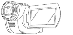
- FIG. 27B is a perspective view of a video camera according to a modification.
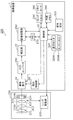
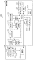
- FIG. 1 is a block diagram showing a configuration of a camera 200 according to the embodiment.
- the camera 200 includes a lens barrel 230 and the imaging device 1.
- the lens barrel 230 includes an optical system 210 and a lens driving unit 220.
- the optical system 210 is composed of one or more lenses that collect external light on the imaging device 10 of the imaging device 1.
- the optical system 210 includes a zoom lens 211, a camera shake correction lens 212, a focus lens 213, and a diaphragm 214.
- the subject image can be enlarged or reduced by moving the zoom lens 211 along the optical axis 210A.
- the focus of the subject image can be adjusted by moving the focus lens 213 along the optical axis 210A.
- the camera shake correction lens 212 is movable in a plane perpendicular to the optical axis 210A of the optical system 210. By moving the camera shake correction lens 212 in a direction to cancel the camera 200 shake, the influence of the camera 200 shake on the captured image can be reduced.
- the diaphragm 214 has an opening 214A located on the optical axis 210A, and adjusts the size of the opening 214A according to the setting of the user or automatically to adjust the amount of transmitted light.
- the lens driving unit 220 includes a zoom actuator that drives the zoom lens 211, a camera shake correction actuator that drives the camera shake correction lens 212, a focus actuator that drives the focus lens 213, and a diaphragm actuator that drives the diaphragm 214.
- the lens driving unit 220 controls the zoom actuator, the focus actuator, the camera shake correction actuator, and the aperture actuator.
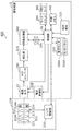
- the imaging device 1 includes an imaging device 10, a correction unit 15, a voltage control unit 20, a control unit 50, an A / D converter 250, an image processing unit 260, a memory 270, a card slot 290, and an internal memory. 340, the operation member 310, and the display monitor 320 are comprised.
- the imaging device 10 outputs a signal frame image (described later) and a light-shielded frame image (described later) at a predetermined frame period T1 (for example, 1/60 seconds).
- the A / D converter 250 increases the analog gain of the analog image data generated by the image sensor 10 and converts it to digital image data that is a digital signal.
- the correction unit 15 reduces the dark current signal component with respect to at least a part of one or more frame images (here, digital image data converted by the A / D converter 250) output from the image sensor 10. Correct as follows.
- the correction unit 15 is realized by a processor (not shown) executing a program stored in a memory (not shown).
- the voltage control unit 20 controls a voltage applied to a photoelectric conversion member 111 (described later) included in the image sensor 10.
- the voltage control unit 20 is realized by a processor (not shown) executing a program stored in a memory (not shown).
- the image processing unit 260 performs various processes on the image data generated by the image sensor 10 (here, the frame image corrected by the correction unit 15), and generates image data to be displayed on the display monitor 320. Or image data to be stored in the memory card 300 is generated.
- the image processing unit 260 performs various processes such as gamma correction and white balance correction on the image data generated by the image sensor 10.
- the image processing unit 260 converts the image data generated by the image sensor 10 into H.264. It compresses by the compression format etc. based on H.264 standard or MPEG2 standard.
- the image processing unit 260 is realized by a processor (not shown) executing a program stored in a memory (not shown).
- the control unit 50 controls the entire camera 200.
- the control unit 50 is realized by developing a program recorded in the internal memory 340 in the memory 270 that temporarily stores the program and executing a processor (not shown) in the control unit 50. .
- the memory 270 also functions as a work memory for the image processing unit 360 and the control unit 50.
- the memory 270 can be realized by, for example, a DRAM or an SRAM.
- the card slot 390 holds the memory card 300 in a removable manner.
- the card slot 290 can be mechanically and electrically connected to the memory card 300.
- the memory card 300 includes a nonvolatile flash memory, a ferroelectric memory, and the like, and can store data such as an image file generated by the image processing unit 260.
- the internal memory 340 is configured by a nonvolatile flash memory, a ferroelectric memory, or the like.
- the internal memory 340 stores a control program for controlling the entire camera 200 and the like.
- the operation member 310 is a generic term for a user interface that receives an operation from a user.
- the operation member 310 includes, for example, a cross key that accepts an operation from the user, a determination button, and the like.
- the display monitor 320 includes a screen 320A that can display an image indicated by the image data generated by the image sensor 10 and an image indicated by the image data read from the memory card 300.
- the display monitor 320 can also display various menu screens for performing various settings of the camera 200 on the screen 320A.
- a touch panel 320B is arranged on the screen 320A of the display monitor 320. The touch panel 320B can be touched by the user and accept various touch operations. The instruction indicated by the touch operation on the touch panel 320B is notified to the control unit 50 and various processes are performed.
- the imaging device 1 the imaging device 10, the correction unit 15, and the voltage control unit 20 will be described in more detail with reference to the drawings.
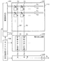
- FIG. 2 is a block diagram showing the configuration of the image sensor 10.
- the image sensor 10 includes a photoelectric conversion element 110, a pixel circuit array 120, a readout circuit 130, an output circuit 140, a row scanning circuit 150, a timing control circuit 160, and a voltage application circuit. 170.
- FIG. 3A is a plan view of the photoelectric conversion element 110
- FIG. 3B is a side view of the photoelectric conversion element 110.
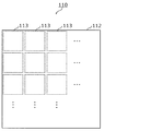
- the photoelectric conversion element 110 is in close contact with the thin-film photoelectric conversion member 111, the upper transparent electrode 112 that is in close contact with the upper surface of the photoelectric conversion member 111, and the lower surface of the photoelectric conversion member 111.
- N ⁇ M lower pixel electrodes 113 arranged in a two-dimensional array of N rows and M columns (N and M are integers of 1 or more).
- the photoelectric conversion member 111 generates charges due to the internal photoelectric effect by receiving light in a state where a first predetermined range voltage not including 0V is applied, and in a state where a second predetermined range voltage including 0V is applied. Even if light is received, no charge is generated by the internal photoelectric effect.
- the photoelectric conversion member 111 is an organic thin film having the above characteristics. That is, in this embodiment, the image pickup device 10 is an example of an organic CMOS image sensor that uses an organic thin film as a photoelectric conversion member.
- the upper transparent electrode 112 is a transparent electrode that applies a voltage that generates a potential difference including 0 to the lower surface over the entire upper surface of the photoelectric conversion member 111.
- the lower pixel electrode 113 is an electrode arranged in a two-dimensional array of N rows and M columns so as to cover the entire lower surface of the photoelectric conversion member 111.
- the lower pixel electrode 113 is formed in the vicinity of itself when a charge is generated on the upper surface of the photoelectric conversion member 111 so as to generate a positive potential difference with respect to the lower surface. Among the generated charges, positive charges are collected.
- the photoelectric conversion element 110 configured as described above has an internal photoelectric effect due to light reception under a condition in which a voltage causing a positive potential difference in a range in which the internal photoelectric effect is generated is applied to the upper surface of the photoelectric conversion member 111 with respect to the lower surface.
- Each of the lower pixel electrodes 113 collects the positive charges generated by the above. That is, the photoelectric conversion element 110 is in an exposed state under this condition.
- the photoelectric conversion element 110 under the condition that the upper surface of the photoelectric conversion member 111 has substantially the same potential as the lower surface, even if light is received, no charge is generated due to the internal photoelectric effect, and therefore each of the lower pixel electrodes 113 has a charge. There is no current collection. That is, the photoelectric conversion element 110 is in a light shielding state under this condition.
- a period in which a voltage causing a positive potential difference in a range in which the internal photoelectric effect occurs is applied to the upper surface of the photoelectric conversion member 111 as an exposure period.
- a period in which a voltage in a range where the internal photoelectric effect does not occur is applied to the lower surface is referred to as a light shielding period.
- the pixel circuit array 120 is a semiconductor device in which N ⁇ M pixel circuits 21 are arranged in a two-dimensional array of N rows and M columns, and the photoelectric conversion element 110 is arranged on the lower surface side of the photoelectric conversion element 110. Arranged in a superimposed manner.
- each pixel circuit 21 is arranged so that the position of each pixel circuit 21 overlaps with the position of each lower pixel electrode 113 in a one-to-one correspondence when the imaging device 10 is viewed in plan. Has been.
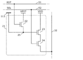
- FIG. 4 is a block diagram showing the configuration of the pixel circuit 21. As shown in FIG. 4
- the pixel circuit 21 includes a reset transistor 22, an amplification transistor 23, a selection transistor 24, and a charge storage node 25.
- the charge storage node 25 is connected to the lower pixel electrode 113 corresponding to the pixel circuit 21 to which the charge storage node 25 belongs, the source of the reset transistor 22, and the gate of the amplification transistor 23, and is collected by the connected lower pixel electrode 113. Accumulate positive charge.
- the reset transistor 22 has a gate connected to the reset signal line 51, a drain supplied with a reset voltage VRST, and a source connected to the charge storage node 25.
- the reset transistor 22 is turned on by a reset signal delivered from the row scanning circuit 150 (described later) via the reset signal line 51, thereby resetting (initializing) the amount of charge accumulated in the charge accumulation node 25. To do.
- the charge storage node 25 is connected to the gate, the power supply voltage VDD is supplied to the drain, and the drain of the selection transistor 24 is connected to the source.
- a voltage corresponding to the charge accumulated in the charge accumulation node 25 is applied to the gate of the amplification transistor 23.
- the amplifying transistor 23 functions as a current source for supplying a current corresponding to the charge stored in the charge storage node 25 when the selection transistor 24 is in the ON state.
- the selection signal line 52 is connected to the gate, the source of the amplification transistor 23 is connected to the drain, and the vertical signal line 32 is connected to the source.
- the selection transistor 24 is turned on by a selection signal delivered from the row scanning circuit 150 (described later) via the selection signal line 52, thereby outputting a current flowing through the amplification transistor 23 to the vertical signal line 32.
- the pixel circuit 21 accumulates the charge generated by the photoelectric conversion member 111 in the charge accumulation node 25 in units of pixels with the above configuration. Then, the amount of charge stored in the charge storage node 25 is read out nondestructively.
- the row scanning circuit 150 has the following stored charge amount reset function and the following readout pixel circuit selection function.
- the accumulated charge amount resetting function is sequentially performed row by row from the row farthest to the readout circuit 130 (first row) to the row closest to the readout circuit 130 (Nth row).
- the reset signal for resetting the positive charge accumulated in the charge accumulation node 25 in each pixel circuit 21 belonging to the relevant row is delivered via the reset signal line 51 connected to each pixel circuit 21 belonging to the relevant row. It is a function to do.
- the resetting of the charges accumulated in the charge accumulation nodes 25 of all the pixel circuits 21 included in the pixel circuit array 120 is sequentially executed in units of rows from the first row to the Nth row.
- the readout pixel circuit selection function refers to a selection signal for turning on the selection transistor 24 in each of the pixel circuits 21 belonging to the corresponding row in order from the first row to the Nth row in the pixel circuit array 120. This is a function of delivering via the selection signal line 52 connected to each pixel circuit 21 belonging to the corresponding row.
- the reading of the charge amount accumulated in the charge accumulation nodes 25 of all the pixel circuits 21 included in the pixel circuit array 120 is sequentially executed in units of rows from the first row to the Nth row.
- the readout circuit 130 reads out the amount of charge accumulated in each of the pixel circuits 21 constituting the pixel circuit array 120.
- the readout circuit 130 is configured to include M column readout circuits 31 corresponding to the M columns of the pixel circuit array 120, respectively.
- the column readout circuit 31 includes a selection transistor 24 that is turned on by a selection signal via a vertical signal line 32 connected to each of the pixel circuits 21 belonging to the corresponding column (this pixel circuit 21). Is also referred to as “a pixel circuit 21 to be read”.), By detecting the amount of current flowing through the amplification transistor 23, the amount of charge accumulated in the charge accumulation node 25 of the pixel circuit 21 to be read is read. Then, a digital signal of K bits (K is a positive integer, for example, 8) indicating the amount of the read electric charge is output as a pixel value of the pixel circuit 21 to be read.
- the output circuit 140 outputs a frame image composed of the pixel values output from the column readout circuit 31 to the outside.
- the frame image output from the output circuit 140 includes a signal frame image based on the amount of charge accumulated in the charge accumulation node 25 of each pixel circuit 21 and the photoelectric conversion element 110 during the period in which the photoelectric conversion element 110 is in the exposure state. There is a light-shielded frame image based on the amount of charge accumulated in the charge accumulation node 25 of each pixel circuit 21 during the light-shielded state.
- the charge accumulated in the charge accumulation node 25 of each pixel circuit 21 during the period when the photoelectric conversion element 110 is in the light-shielding state is a dark current component of each pixel circuit 21.
- the light-shielded frame image is a frame image made up of dark current components of each pixel circuit 21.
- the voltage application circuit 170 applies a voltage to the photoelectric conversion member 111. More specifically, the voltage application circuit 170 controls the voltage applied to the upper transparent electrode 112 so that (1) the lower surface of the photoelectric conversion member 111 has a positive potential difference that causes the internal photoelectric effect.
- the photoelectric conversion element 110 is set as the exposure period during the application state, and (2) a positive potential difference that causes the internal photoelectric effect is generated on the lower surface.
- the photoelectric conversion element 110 is set as a light shielding period during the application state.
- the timing control circuit 160 controls the operation timing of the row scanning circuit 150, the operation timing of the readout circuit 130, the operation timing of the voltage application circuit 170, and the operation timing of the output circuit 140. That is, the timing control circuit 160 controls the timing for executing the stored charge amount reset function and the timing for executing the readout pixel circuit selection function by the row scanning circuit 150, and is selected by the selection signal by the readout circuit 130.
- the timing at which the amount of charge accumulated in the charge accumulation node 25 of the pixel circuit 21 is read is controlled, the timing at which the voltage conversion circuit 110 sets the photoelectric conversion element 110 as the exposure period, and the photoelectric conversion element 110 as the light shielding period.
- the timing of outputting a frame image by the output circuit 140 is controlled.
- the timing control circuit 160 when the timing control circuit 160 receives a frame start signal (described later) from the voltage control unit 20, the timing control circuit 160 performs the row scanning circuit 150, the readout circuit 130, the voltage application circuit 170, and the output circuit 140. By controlling the operation timing, (1) the charge amount accumulated in the charge accumulation nodes 25 of all the pixel circuits 21 included in the pixel circuit array 120 is read, and (2) based on the read charge amount. A frame image is output to the outside as a light-shielded frame image, (3) the charge amount accumulated in the charge accumulation nodes 25 of all the pixel circuits 21 included in the pixel circuit array 120 is reset, and (4) a photoelectric conversion member Application of the first voltage to 111 is started.
- a frame start signal described later
- the timing control circuit 160 When the timing control circuit 160 receives an exposure shading switching signal (described later) from the voltage control unit 20, the timing control circuit 160 determines the operation timing of the row scanning circuit 150, the readout circuit 130, the voltage application circuit 170, and the output circuit 140. And (1) read out the charge amount accumulated in the charge accumulation nodes 25 of all the pixel circuits 21 included in the pixel circuit array 120, and (2) read out the frame image based on the read charge amount. The signal frame image is output to the outside, (3) the charge amount accumulated in the charge accumulation nodes 25 of all the pixel circuits 21 included in the pixel circuit array 120 is reset, and (4) the photoelectric conversion member 111 Application of the second voltage is started. Returning to FIG. 1 again, the description of the imaging device 1 will be continued.
- the voltage control unit 20 applies a first voltage in a first predetermined range to the photoelectric conversion member 111 during a part of the exposure period in the frame period T1 every predetermined frame period T1, and the voltage period in the frame period T1.
- the voltage applied to the photoelectric conversion member 111 is controlled such that the second voltage in the second predetermined range is applied to the photoelectric conversion member 111 during the light shielding period that does not include the exposure period. More specifically, a frame start signal for starting a new frame cycle is output to the image sensor 10 at a frame cycle T1, and the phase is delayed by a predetermined period T2 from the frame start signal output.
- By controlling the voltage applied to the photoelectric conversion member 111 by outputting an exposure shading switching signal for switching the voltage applied to the photoelectric conversion member 111 from the first voltage to the second voltage at the frame period T1. .
- FIG. 5A is a timing chart of a frame start signal and an exposure shading switching signal output by the voltage control unit 20.
- FIG. 5B is a timing chart showing the operation of the image sensor 10 when a frame start signal and an exposure shading switching signal are received from the voltage control unit 20.
- the voltage control unit 20 provides the image sensor 10 with a frame start signal and an exposure shading switching signal for each frame period T1, and the exposure shading switching signal for a predetermined period from the frame start signal.
- the output is made so as to be delayed by T2 (T2 ⁇ T1).
- the image sensor 10 when receiving the frame start signal and the exposure shading switching signal output from the voltage control unit 20 for each frame period T1, the image sensor 10 receives the frame start signal and then executes the next. During the period until the exposure shading switching signal is received, the first voltage is applied to the photoelectric conversion member 111, and after the exposure shading switching signal is received until the next frame start signal is received, the photoelectric conversion member 111 receives the second voltage. Apply voltage.
- the photoelectric conversion element 110 is in an exposure state during the period from the reception of the frame start signal to the next reception of the exposure shading switching signal, and from the reception of the exposure shading switching signal to the next reception of the frame start signal. During this period, the light is blocked.
- the imaging element 10 reads out the charge amount accumulated in the charge accumulation node 25 of each pixel circuit 21 during the exposure period in which the photoelectric conversion element 110 is in an exposure state, and outputs a signal frame image based on the read charge amount. Then, during the light shielding period in which the photoelectric conversion element 110 is in the light shielding state, the charge amount accumulated in the charge accumulation node 25 of each pixel circuit 21 is read, and a light shielding frame image based on the read charge amount is output.
- the correction unit 15 corrects the signal frame image output from the image sensor 10 so as to reduce the dark current signal component using the light-shielded frame image output from the image sensor 10.
- correction unit 15 applies a signal frame image to be corrected (hereinafter referred to as “correction target signal frame image”) in the same frame cycle as the frame cycle in which the correction target signal frame image is output. Correction is performed using the output light-shielding frame image (hereinafter referred to as “correction light-shielding frame image”).
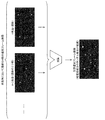
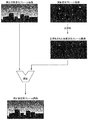
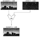
- FIG. 6 is a schematic diagram showing a state of correction performed by the correction unit 15.
- white dots included in the correction target signal frame image and the correction light-shielding frame image schematically represent the dark current signal component in the corresponding pixel.
- a dark current signal component called a “white scratch” may appear as a white point on a frame image.
- the correction target signal frame image is an image in which a dark current signal component is superimposed on an image of a subject
- the correction light-shielding frame image is an image including a dark current signal component
- the correction unit 15 performs a normalization process on the correction light-shielding frame image to generate a normalized light-shielding frame image.
- the normalization process is a process for normalizing the light-shielded state period (light-shielded period Ts) in the correction light-shielded frame image with the exposure state period (exposure period Tr) in the correction target signal frame image.
- the correction unit 15 generates a normalized light-shielding frame image by multiplying each pixel value of the light-shielding frame image for correction by the value of (exposure period Tr / light-shielding period Ts). To do.
- the dark current signal component in the normalized shading frame image is (Tr / Ts) times the dark current signal component in the correction shading frame image.
- Tr the dark current signal component in the normalized shading frame image
- Tr the dark current signal component in the correction shading frame image.
- the correction unit 15 subtracts the corresponding pixel value of each pixel of the normalized shading frame image from the pixel value of each pixel of the correction target signal frame image, thereby correcting the signal frame image after correction. Is generated.
- the correction unit 15 performs the above processing to generate a corrected signal frame image in which the dark current signal component is reduced from the correction target signal frame image.
- the imaging device 1 performs a first frame image output process and a first correction process as characteristic operations.
- the first frame image output process is a process in which the image sensor 10 alternately outputs a signal frame image and a light-shielded frame image at a predetermined frame period T1.
- the applied voltage to the photoelectric conversion member 111 is the second voltage (eg, 0 V here) in the initial state before the first frame image output process is started.
- the first frame image output process is started when the user using the imaging device 1 receives an operation to start capturing a moving image.
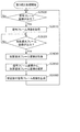
- FIG. 7 is a flowchart of the first frame image output process.
- the voltage control unit 20 When the first frame image output process is started, the voltage control unit 20 outputs a frame start signal to the image sensor 10 (step S5).
- the image sensor 10 When the image sensor 10 receives the frame start signal output from the voltage controller 20, the image sensor 10 reads the amount of charge accumulated in the charge accumulation node 25 of each pixel circuit 21 included in the pixel circuit array 120 (step S10). A light shielding frame image based on the read charge amount is output (step S15).
- the image sensor 10 changes the voltage applied to the photoelectric conversion member 111 from the second voltage to the first voltage (here, 10 V, for example) (step S20).
- the state of the photoelectric conversion element 110 is switched from the light shielding state to the exposure state (step S25).
- the image sensor 10 resets the amount of charge accumulated in the charge accumulation node 25 of each pixel circuit 21 included in the pixel circuit array 120 (step S30).
- the voltage control unit 20 outputs an exposure shading switching signal to the image sensor 10 when a predetermined period T2 has elapsed since the last frame start signal was output (Step S35: Yes after repeating Step S35: Yes). Output (step S40).
- the image sensor 10 When the image sensor 10 receives the exposure shading switching signal output from the voltage controller 20, the image sensor 10 reads the amount of charge accumulated in the charge accumulation node 25 of each pixel circuit 21 included in the pixel circuit array 120 (step S45). Then, an exposure frame image based on the read charge amount is output (step S50).
- the imaging device 10 changes the voltage applied to the photoelectric conversion member 111 from the first voltage to the second voltage (step S55).
- step S60 the state of the photoelectric conversion element 110 is switched from the exposure state to the light shielding state.
- the image sensor 10 resets the charge amount accumulated in the charge accumulation node 25 of each pixel circuit 21 included in the pixel circuit array 120 (step S65).
- step S70 when a predetermined time T1 has elapsed since the last frame start signal was output (step S70: No is repeated and then step S70: Yes), the image sensor 10 proceeds to the process of step S5 and repeats the subsequent processes. .
- the correction unit 15 reduces the target and the dark current signal component by using the light-shielded frame image output from the image sensor 10 for the signal frame image output from the image sensor 10. This is a correction process.
- the first correction process is started when the first light-shielded frame image is output from the image sensor 10 in the first frame image output process described above.
- FIG. 8 is a flowchart of the first correction process.
- the correction unit 15 waits until a signal frame image is output from the image sensor 10. Then, when the signal frame image is output while waiting for the output of the signal frame image (Step S100: Yes after repeating Step S100: Yes), the correction unit 15 acquires the signal frame image (Step S110). ).
- the correction unit 15 waits until the light shielding frame image is output from the image sensor 10.
- the correction unit 15 acquires the light shielding frame image (Step S130). ).
- the correction unit 15 performs a normalization process on the acquired shading frame image to generate a normalized shading frame image (step S140). That is, the correction unit 15 generates a normalized shading frame image by multiplying each pixel value of the acquired shading frame image by a value of (Tr / Ts).
- the correction unit 15 calculates the pixel value of each pixel of the normalized shading frame image corresponding to the pixel value of each pixel of the acquired signal frame image. By subtracting (step S150), a corrected signal frame image is generated (step S160).
- step S160 When the process of step S160 is completed, the correction unit 15 proceeds to the process of step S100 and repeats the subsequent processes.
- the imaging device 1 uses the light-shielded frame image output from the image sensor 10 in the same frame period for the signal frame image output from the image sensor 10 at the predetermined frame period T1, and uses the dark current. Perform correction to reduce signal components.
- the dark current signal component varies depending on the temperature of the image sensor and the like. For this reason, when the temperature of the image sensor changes during the imaging period of continuous frame images, the dark current signal component changes. Therefore, according to the imaging apparatus 1 according to the present embodiment, the dark current signal component during the imaging period of the continuous signal frame images cannot be acquired, and the imaging apparatus 1 can perform more accurately during the imaging period. The dark current signal component included in the captured frame image can be reduced.
- Modification 1 an imaging apparatus according to Modification 1 in which some of the functions are changed from the imaging apparatus 1 according to the embodiment will be described with reference to the drawings.
- the correction unit 15 is normalized by multiplying each pixel value of the correction light-shielding frame image by a value of (exposure period Tr) / (light-shielding period Ts).
- the corrected signal frame image is generated by subtracting the pixel value of each pixel of the corresponding normalized shading frame image from each pixel value of the correction target signal frame image. It was an example of a configuration to do.
- the exposure period Tr and the light shielding period Ts are set equal to each other, and the correction unit performs correction corresponding to each pixel value of the correction target signal frame image.
- the corrected signal frame image is generated by subtracting each pixel of the light-shielded frame image as it is.
- FIG. 9 is a block diagram illustrating a configuration of a camera 900 according to the first modification.
- the camera 900 is modified so that the imaging device 1 is changed to the imaging device 2 from the camera 200 according to the embodiment.
- the imaging device 2 is modified from the imaging device 1 according to the embodiment so that the correction unit 15 is changed to the correction unit 915 and the voltage control unit 20 is changed to the voltage control unit 920.
- the voltage control unit 920 is modified from the voltage control unit 20 according to the embodiment so that a part of its function is changed.
- the voltage control unit 20 outputs a frame start signal to the image sensor 10 at a frame period T1, and further performs exposure at a frame period T1 having a phase delayed by a predetermined period T2 from the frame start signal output.
- This is an example of a configuration in which the voltage applied to the photoelectric conversion member 111 is controlled by outputting a light shielding switching signal.
- the voltage control unit 920 outputs a frame start signal to the image sensor 10 at a frame period T1, and further performs exposure at a frame period T1 that has a phase delayed by T1 / 2 from the frame start signal output. It is an example of a configuration in which the voltage applied to the photoelectric conversion member 111 is controlled by outputting a light shielding switching signal.
- FIG. 10A is a timing chart of a frame start signal and an exposure shading switching signal output by the voltage control unit 920.
- FIG. 10B is a timing chart showing the operation of the image sensor 10 when a frame start signal and an exposure shading switching signal are received from the voltage control unit 920.
- the voltage control unit 920 sends a frame start signal and an exposure shading switching signal to the image sensor 10 every frame period T1, and the exposure shading switching signal is T1 / T1 more than the frame start signal. An output is made so that the timing is delayed by two.
- the image sensor 10 when receiving the frame start signal and the exposure shading switching signal output from the voltage control unit 920 for each frame period T1, the image sensor 10 receives the frame start signal, and then The first voltage is applied to the photoelectric conversion member 111 during the period until the exposure shading switching signal is received, and the second voltage is applied to the photoelectric conversion member 111 during the period from when the exposure shading switching signal is received until the next frame start signal is received. Apply.
- the photoelectric conversion element 110 is in an exposure state for a period from when the frame start signal is received until T1 / 2 elapses, and is shielded from light for the period after T1 / 2 elapses until the next frame start signal is received. It becomes a state.
- the imaging element 10 reads out the charge amount accumulated in the charge accumulation node 25 of each pixel circuit 21 during the exposure period in which the photoelectric conversion element 110 is in an exposure state, and outputs a signal frame image based on the read charge amount. Then, during the light shielding period in which the photoelectric conversion element 110 is in the light shielding state, the charge amount accumulated in the charge accumulation node 25 of each pixel circuit 21 is read, and a signal frame image based on the read charge amount is output.
- the correction unit 915 is modified from the correction unit 15 according to the embodiment so that a part of the function is changed.
- the correction unit 15 multiplies each pixel value of the light-shielding frame image for correction by the value of (exposure period Tr) / (light-shielding period Ts), thereby obtaining a normalized light-shielding frame image.
- the correction unit 915 generates a corrected signal frame image by subtracting each pixel of the corresponding light-shielding frame image for correction as it is from each pixel of the correction target signal frame image. It has become.
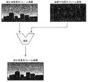
- FIG. 11 is a schematic diagram showing a state of correction performed by the correction unit 915.
- the correction unit 915 subtracts the pixel value of the corresponding light-shielding frame image for correction from each pixel value of the pixel of the correction target signal frame, thereby obtaining the corrected signal frame image. Generate.
- the exposure period Tr and the light shielding period Ts are set equal.
- the correction unit 915 performs an initialization process for initializing the light shielding period Ts with the exposure period Tr in each frame cycle, as in the correction unit 15 according to the embodiment. There is no need.
- the imaging device 2 performs a second frame image output process and a second correction process as characteristic operations.
- the second frame image output process is a process in which the image sensor 10 alternately outputs a signal frame image and a light-shielded frame image with a phase shifted by T1 / 2 from each other at a predetermined frame period T1.
- This second frame image output process is a process in which a part of the process is changed from the first frame image output process according to the embodiment.
- FIG. 12 is a flowchart of the second frame image output process.
- step S1205 to step S1230 and the processing from step S1240 to step S1270 are the same as those in step S5 in the first frame image output processing (see FIG. 7) according to the embodiment.
- the voltage controller 20 is replaced with the voltage controller 920.
- step S1235 the processing before and after that will be described.
- step S1230 After the process of step S1230 is completed, the voltage control unit 920 outputs the previous frame start signal and when T1 / 2 has elapsed (step S1235: No is repeated and then step S1235: Yes), the image sensor 10 On the other hand, an exposure switching signal is output (step S1240).
- the correction unit 915 subtracts each pixel of the corresponding light-shielding frame image as it is from each pixel of the signal frame image output from the image sensor 10, so that the target signal frame image is obtained.
- the correction is performed so as to reduce the dark current component.
- the second correction process is a process in which a part of the process is changed from the first correction process according to the embodiment.
- FIG. 13 is a flowchart of the second correction process.
- step S1300 to step S1330 and the processing from step S1360 are respectively the same as the processing from step S100 to step S130 in the first correction processing according to the embodiment (see FIG. 8).
- the correction unit 15 is replaced with the correction unit 915.
- step S140 in the first correction process according to the embodiment is deleted.
- step S1350 the processing in step S1350 and the processing before and after that will be described.
- the correction unit 915 subtracts the corresponding pixel value of the shaded frame image from the pixel value of each pixel of the acquired signal frame image (step S1350). Thus, a corrected signal frame image is generated (step S1360).
- the correction unit 915 subtracts each pixel value of the corresponding correction light-shielding frame image as it is from each pixel value of the correction target signal frame image, thereby correcting the corrected signal. Generate a frame image.
- the imaging device 2 according to the first modification it is possible to realize the correction of the signal frame image with a smaller calculation amount than the imaging device 1 according to the embodiment.
- Modification 2 an imaging apparatus according to Modification 2 in which some of the functions are changed from the imaging apparatus 1 according to the embodiment will be described with reference to the drawings.
- the imaging apparatus 1 is an example of a configuration in which a correction target signal frame is corrected using a light-shielded frame image output in the same frame period as the correction target signal frame is output.
- the imaging apparatus is configured to correct the correction target signal frame using the light-shielded frame image output in a plurality of frame periods including the frame period in which the correction target signal frame is output. It is an example.
- FIG. 14 is a block diagram illustrating a configuration of a camera 1400 according to the second modification.
- the camera 1400 is modified so that the imaging device 1 is changed to the imaging device 3 from the camera 200 according to the embodiment.
- the imaging apparatus 3 is modified from the imaging apparatus 1 according to the embodiment so that the correction unit 15 is changed to the correction unit 1415 and an added image generation unit 1417 is added.
- the addition image generation unit 1417 generates an addition light shielding frame image by adding pixel values of pixels corresponding to each other in each light shielding frame image to a plurality of light shielding frame images output from the image sensor 10.
- FIG. 15 is a schematic diagram showing a state of generation of the added light-shielded frame image performed by the added image generating unit 1417.
- the addition image generation unit 1417 outputs the image including the newly output light-shielded frame image.
- an added shading frame image is generated by adding pixel values of pixels corresponding to each other in each shading frame image to the latest n (n is an integer of 2 or more) shading frame images in time series.
- n is an integer of 2 or more shading frame images in time series.
- random noise (“random component”) generated at different positions (that is, different pixels) in n light-shielding frame images is added only for one sheet in the added light-shielding frame image. Therefore, the brightness appears sufficiently lower than the “white scratch” added n times, and is hardly noticeable. That is, the “random component” is reduced in the added light-shielded frame image compared to “white scratches”. Even if random noise is generated at the same position in a plurality of light-shielding frame images among n light-shielding frame images, it is not a problem because it is less than the number of “white scratches”.
- the correction unit 1415 is modified from the correction unit 15 according to the embodiment so that a part of its function is changed.
- the correction unit 15 is an example of a configuration in which a correction target signal frame is corrected using a light-shielded frame image output in the same frame period as that of the correction target signal frame.
- the correction unit 1415 includes, as an addition target, a light shielding frame image output from the addition image generation unit 1417 that includes a light shielding frame image output in the same frame period as the frame period in which the correction target signal frame is output. This is an example of a configuration for correcting the signal frame to be corrected using.
- FIG. 16 is a schematic diagram showing how correction is performed by the correction unit 1415.
- the correction unit 1415 performs a normalization process on the added shading frame image to generate a normalized added shading frame image.
- the normalization process refers to a process of normalizing the total of the light shielding periods (n ⁇ Ts) in the added light shielding frame image with the exposure period (Tr) in the correction target signal frame image. More specifically, the correction unit 1415 generates a normalized added shading frame image by multiplying each pixel value of the added shading frame image by a value of (Tr / (n ⁇ Ts)). To do. Thereby, the dark current signal component in the normalized addition light-shielding frame image is (Tr / (n ⁇ Ts)) times the dark current signal component in the addition light-shielding frame image.
- Tr ⁇ (n ⁇ Ts) is an example.
- the brightness of the so-called “white scratch” and “random component” in the normalized added shading frame image is the so-called “white scratch” and “random” in the added shading frame image. It becomes smaller than the brightness of “component”.
- the absolute value can be reduced by normalization. Further, for example, if a threshold value that does not include the “random component” is provided in the luminance level for performing the normalization process and the luminance equal to or lower than the threshold value is set to 0, the “random component” can be further reduced.
- the correction unit 1415 subtracts the corresponding pixel value of each pixel of the normalized addition shading frame from the pixel value of each pixel of the correction target signal frame image, thereby correcting the signal frame image after correction. Is generated.
- the imaging device 3 performs a first frame image output process and a third correction process as characteristic operations.
- the correction unit 1415 reduces the dark current signal component by using the added shading frame image output from the added image generation unit 1417 for the signal frame image output from the image sensor 10. This is a process of correcting to.
- This third correction process is started by outputting the (n-1) th light-shielded frame image from the image sensor 10 in the first frame image output process described above.
- FIG. 17 is a flowchart of the third correction process.
- the correction unit 1415 waits until a signal frame image is output from the image sensor 10.
- the correction unit 1415 acquires the signal frame image (step S1710). ).
- the correction unit 1415 waits until the addition light shielding frame image is output from the addition image generation unit 1417. Then, when the addition light-shielding frame image is output while waiting for the output of the additional light-shielding frame image (step S1720: No is repeated and then step S1720: Yes), the correction unit 1415 acquires the additional light-shielding frame image. (Step S1730).
- the correction unit 1415 performs a normalization process on the acquired added shading frame image to generate a normalized adding shading frame image (step S1740). That is, the correction unit 15 generates a normalized added light-shielded frame image by multiplying each pixel value of the acquired added light-shielded frame image by a value of (Tr / (n ⁇ Ts)).
- the correction unit 1415 corresponds to the pixel value of each pixel of the acquired signal frame image, and the corresponding pixel of each pixel of the normalized addition shading frame image. By subtracting the value (step S1750), a corrected signal frame image is generated (step S1760).
- step S1760 the correction unit 1415 proceeds to the process of step S1700 and repeats the subsequent processes.
- the added shading frame image generated by the adding image generation unit 1417 is reduced by averaging the random components of the dark current components in each of the n shading frame images. Image.
- the signal frame image can be corrected with higher accuracy than the imaging device 1 according to the embodiment.
- Modification 3 an imaging apparatus according to Modification 3 in which some of the functions of the imaging apparatus 2 according to Modification 1 are changed will be described with reference to the drawings.
- the exposure period Tr and the light shielding period Ts are set to be equal, and the same frame period as the frame period in which the correction target signal frame is output for each pixel of the correction target signal frame image.
- the corrected signal frame image is generated by subtracting the pixel value of each pixel of the light-shielded frame image output in the cycle as it is.
- the imaging apparatus is the same in that the exposure period Tr and the light shielding period Ts are set equal, but the light shielding frame image to be subtracted from the correction target signal frame is To be changed to an added blocked average light frame image obtained by averaging the pixels of the shaded frame image output in a plurality of frame periods including the frame period in which the correction target signal frame is output.
- This is an example of a deformed configuration.
- FIG. 18 is a block diagram illustrating a configuration of a camera 1800 according to the third modification.
- the camera 1800 is modified from the camera 900 according to Modification 1 so that the imaging device 2 is changed to the imaging device 4.
- the imaging apparatus 4 is modified from the imaging apparatus 2 according to the first modification so that the correction unit 915 is changed to the correction unit 1815 and an addition average image generation unit 1817 is added.
- the addition average image generation unit 1817 generates an addition average light shielding frame image by averaging the pixel values of pixels corresponding to each other in each light shielding frame image with respect to the plurality of light shielding frame images output from the image sensor 10. .
- FIG. 19 is a schematic diagram showing a state of generation of an addition average shading frame image performed by the addition average image generation unit 1817.
- the addition average image generation unit 1817 outputs the image from the image sensor 10 including the newly output light-shielded frame image.
- an addition average shading frame image is generated by adding and averaging pixel values of corresponding pixels in each shading frame image with respect to the latest n (n is an integer of 2 or more) shading frame images in time series. To do.
- the dark current signal components at the same position (that is, the same pixel) in the n light-shielding frame images are added as the dark current signal components at the corresponding position (that is, the corresponding pixel) in the addition average light-shielding frame image. Averaged. For this reason, as illustrated in FIG.
- the added light-shielded frame image generated by the averaging process is an image in which the random component of the dark current component in each of the n light-shielded frame images is reduced.
- the addition average light-shielding frame image generated by the addition average image generation unit 1817 is an image that is reduced by averaging the random components of the dark current components in each of the n light-shielding frame images. ing.
- the correction unit 1815 is modified from the correction unit 915 according to Modification 1 so that a part of the function is changed.
- the correction unit 915 uses the pixel value of each pixel of the light-shielded frame image output in the same frame period as that of the correction target signal frame for each pixel of the correction target signal frame image. This is an example of a configuration in which a signal frame image after correction is generated by subtracting as it is.
- the correction unit 1815 uses the light-shielded frame image output in the same frame period as the frame period in which the correction target signal frame is output as the average of the light-shielded frame image to be subtracted from the correction target signal frame. It is an example of the structure modified so that it may be changed to the addition average shading frame image output from the addition average image generation unit 1817.
- FIG. 20 is a schematic diagram showing how correction is performed by the correction unit 1815.
- the correction unit 1815 subtracts the pixel value of the corresponding added average light-shielded frame image from the pixel value of the pixel of the correction target signal frame, thereby obtaining the corrected signal frame image. Generate.
- the imaging device 4 performs a second frame image output process and a fourth correction process as characteristic operations.
- the correction unit 1815 uses the pixel value of each pixel that forms the signal frame image output from the image sensor 10, and the pixels that form the addition average light-shielded frame image generated by the addition average image generation unit 1817. Is a process of correcting the target signal frame image so as to reduce the dark current signal component.
- the fourth correction process is started by outputting the (n-1) th light-shielded frame image from the image sensor 10 in the first frame image output process described above.
- FIG. 21 is a flowchart of the fourth correction process.
- the correction unit 1815 waits until the signal frame image is output from the image sensor 10. Then, when the signal frame image is output while waiting for the output of the signal frame image (step S2100: No after repeating step S2100: Yes), the correction unit 1815 acquires the signal frame image (step S2110). ).
- the correction unit 1815 waits until the addition average light shielding frame image is output from the addition average image generation unit 1817. Then, when the addition average light-shielding frame image is output while waiting for the output of the addition average light-shielding frame image (Step S2120: Yes after repeating Step S2120), the correction average light-shielding frame image is output. Is acquired (step S2130).
- the correction unit 1815 subtracts the corresponding pixel value of each pixel of the acquired averaged light-shielded frame image from the pixel value of each pixel of the acquired signal frame image (step S2150), thereby correcting the pixel value.
- the signal frame image is generated (step S2160).
- step S2160 When the process of step S2160 is completed, the correction unit 1815 proceeds to the process of step S2100 and repeats the subsequent processes.
- the addition average light shielding frame image generated by the addition average image generation unit 1817 is reduced by averaging the random components of the dark current components in each of the n light shielding frame images. The resulting image.
- the signal frame image can be corrected with higher accuracy than the imaging device 2 according to the first modification.
- Modification 4 an imaging apparatus according to Modification 4 in which some of the functions are changed from the imaging apparatus 3 according to Modification 2 will be described with reference to the drawings.
- the correction unit 1415 calculates (exposure period Tr) / (n ⁇ (light shielding period) for each pixel value of the added light shielding frame image obtained by adding n light shielding frame images. By multiplying the value of Ts)), a normalized added shading frame image is generated, and for each pixel value of the correction target signal frame image, each pixel of the corresponding normalized added shading frame image is In this example, the corrected signal frame image is generated by subtracting the pixel value.
- the exposure period Tr is set to be n times the light shielding period Ts, and the correction unit performs the correction on each pixel value of the correction target signal frame image.
- This is an example of a configuration in which a corrected signal frame image is generated by subtracting each pixel value of the corresponding added light-shielded frame image as it is.
- FIG. 22 is a block diagram illustrating a configuration of a camera 2200 according to the fourth modification.
- the camera 2200 is modified from the camera 1400 according to the modified example 2 so that the imaging device 3 is changed to the imaging device 5.
- the imaging device 5 is modified from the imaging device 3 according to Modification 2 so that the correction unit 1415 is changed to the correction unit 2215 and the voltage control unit 20 is changed to the voltage control unit 2220.
- the voltage control unit 2220 is modified from the voltage control unit 20 according to the second modification so that a part of its function is changed.
- the voltage control unit 20 outputs a frame start signal to the image sensor 10 at a frame period T1, and further performs exposure at a frame period T1 that has a phase delayed by a predetermined period T2 from the frame start signal.
- This is an example of a configuration in which the voltage applied to the photoelectric conversion member 111 is controlled by outputting a light shielding switching signal.
- the voltage control unit 2220 outputs a frame start signal to the image sensor 10 at a frame period T1, and further has a phase delayed by (n / (n + 1)) ⁇ T1 from the frame start signal output.
- This is an example of a configuration in which the voltage applied to the photoelectric conversion member 111 is controlled by outputting the exposure shading switching signal at the frame period T1.
- FIG. 23A is a timing chart of a frame start signal and an exposure shading switching signal output by the voltage control unit 2220.
- FIG. 23B is a timing chart showing the operation of the image sensor 10 when a frame start signal and an exposure shading switching signal are received from the voltage controller 2220.
- the voltage control unit 2220 gives the image sensor 10 a frame start signal and an exposure shading switching signal for each frame period T1, and the exposure shading switching signal is (n greater than the frame start signal). / (N + 1)) ⁇ T1 is output so as to be delayed by T1.
- the image sensor 10 when receiving the frame start signal and the exposure shading switching signal output for each frame period T1 from the voltage control unit 2220, the image sensor 10 receives the frame start signal, and then The first voltage is applied to the photoelectric conversion member 111 during the period until the exposure shading switching signal is received, and the second voltage is applied to the photoelectric conversion member 111 during the period from when the exposure shading switching signal is received until the next frame start signal is received. Apply.
- the photoelectric conversion element 110 is in an exposure state from the reception of the frame start signal until (n / (n + 1)) ⁇ T1 elapses, and after (n / (n + 1)) ⁇ T1 elapses, Next, it is in a light shielding state until a frame start signal is received.
- the imaging element 10 reads out the charge amount accumulated in the charge accumulation node 25 of each pixel circuit 21 during the exposure period in which the photoelectric conversion element 110 is in an exposure state, and outputs a signal frame image based on the read charge amount. Then, during the light shielding period in which the photoelectric conversion element 110 is in the light shielding state, the charge amount accumulated in the charge accumulation node 25 of each pixel circuit 21 is read, and a signal frame image based on the read charge amount is output.
- the correction unit 2215 is modified from the correction unit 1415 according to the second modification so that a part of the function is changed.
- the correction unit 1415 generates a normalized added shading frame image by multiplying each pixel value of the added shading frame image by a value of (Tr / (n ⁇ Ts)).
- This is an example of a configuration in which a corrected signal frame image is generated by subtracting the pixel value of each pixel of the corresponding normalized added light-shielded frame image from each pixel value of the correction target signal frame image. It was.
- the correction unit 2215 generates a corrected signal frame image by subtracting each pixel of the corresponding added light-shielded frame image as it is from each pixel of the correction target signal frame image. It has become.
- FIG. 24 is a schematic diagram showing how correction is performed by the correction unit 2215.
- the correction unit 2215 generates a corrected signal frame image by subtracting the pixel value of the corresponding added shading frame image from the pixel value of the pixel of the correction target signal frame. To do.
- the exposure period Tr is set to be n times the light shielding period Ts.
- the correction unit 2215 calculates the total sum (n ⁇ Ts) of the light-shielded state for the added light-shielded frame image and the exposure state in the correction target signal frame image. There is no need to perform normalization processing to normalize in the period (Tr).
- the imaging device 5 performs a third frame image output process and a fifth correction process as characteristic operations.
- the image sensor 10 has a signal frame image and a light-shielded frame image at a predetermined frame period T1, and the light-shielded frame image is (n / (n + 1)) with respect to the signal frame image. This is a process of alternately outputting at a timing delayed by ⁇ T1.
- This third frame image output process is a process in which a part of the process is changed from the first frame image output process according to the embodiment.
- FIG. 25 is a flowchart of the third frame image output process.
- step S2505 to step S2530 and the processing from step S2540 to step S2570 are the same as those in step S5 in the first frame image output processing (see FIG. 7) according to the embodiment.
- the voltage controller 20 is replaced with the voltage controller 920.
- step S2535 the processing before and after that will be described.
- step S2530 After the processing of step S2530 is completed, the voltage control unit 2220 outputs (n / (n + 1)) ⁇ T1 after outputting the previous frame start signal (step S2535: No is repeated and then step S2535: Yes) ), An exposure switching signal is output to the image sensor 10 (step S2540).
- the correction unit 2215 subtracts each pixel of the corresponding added light-shielded frame image as it is from each pixel of the signal frame image output from the image sensor 10, so that a correction target signal frame image is obtained.
- the correction process is performed so as to reduce the dark current signal component.
- the fourth correction process is a process in which a part of the process is changed from the third correction process according to the second modification.
- FIG. 26 is a flowchart of the fifth correction process.
- step S2600 to step S2630 and the processing from step S2660 are the same as the processing from step S1700 to the processing from step S1730 in the third correction processing according to the second modification (see FIG. 17), respectively.
- the correction unit 915 is replaced with the correction unit 2215.
- step S1740 in the third correction process according to Modification 2 is deleted.
- step S2650 the processing in step S2650 and the processing before and after that will be described.
- step S2630 when the added shading frame image is acquired, the correction unit 2215 subtracts the corresponding pixel value of the added shading frame image from the pixel value of each pixel of the acquired signal frame image (In step S2650), a corrected signal frame image is generated (step S2660).
- the correction unit 2215 subtracts each pixel value of the corresponding added light-shielded frame image as it is from each pixel value of the correction target signal frame image, thereby correcting the signal frame after correction. Generate an image.
- the imaging device 5 according to the fourth modification it is possible to realize the correction of the signal frame image with a smaller calculation amount than the imaging device 3 according to the second modification.
- the photoelectric conversion member 111 generates light due to the internal photoelectric effect by receiving light in a state where a voltage in the first predetermined range is applied, and the voltage in the second predetermined range. It has been described that the organic thin film has a function that does not generate charges due to the internal photoelectric effect even when light is received in a state where is applied.
- the photoelectric conversion member 111 is not necessarily limited to the organic thin film as long as the presence or absence of charge generation due to the internal photoelectric effect can be controlled by the applied voltage.
- the imaging device 1 may be an example in which the photoelectric conversion member 111 is a diode having a PN junction surface.
- the imaging apparatus 1 has been described assuming that the frame period T1 is, for example, 1/60 seconds.
- the frame period T1 is not necessarily limited to 1/60 seconds.
- the imaging apparatus 1 may be an example in which the frame period T1 is 1/50 seconds, an example in which the frame period T1 is set by a user who uses the imaging apparatus 1, and the like.
- the image pickup device 3 includes an image pickup device that includes the newly output light-shielded frame image when the addition image generation unit 1417 outputs a new light-shielded frame image from the image pickup device 10.
- the latest n light-shielding frame images in time series output from 10 are targeted, and the added light-shielding frame image is generated by adding the pixel values of the corresponding pixels in each light-shielding frame image.
- the method for generating the added light-shielded frame image is not necessarily limited to the above method.
- a new shading frame image is added to the already generated summing shading frame image by addition averaging or IIR (Ifinite Impulse Response) is also conceivable.
- pixel values of pixels corresponding to each other in each light-shielded frame image with respect to n light-shielded frame images so that a newer light-shielded frame image is more heavily weighted in time series.
- An example in which an added shading frame image is generated by weighted addition is also conceivable. By doing so, it is possible to reflect more light-shielded frame images output more recently in the reduction of dark current signal components.
- the present disclosure includes an electronic device in which the imaging device 1 according to the embodiment is incorporated.
- Such an electronic device is realized, for example, as a digital still camera shown in FIG. 27A or a video camera shown in FIG. 27B.
- the imaging apparatus 1 has been described as having a configuration separate from the optical system 210.
- the imaging device 1 is not necessarily limited to a configuration that is separate from the optical system 210.
- the imaging device 1 may be a camera with a lens including the optical system 210 and the lens driving unit 220.
- Each component (functional block) in the imaging devices 1 to 5 may be individually made into one chip by a semiconductor device such as an IC (Integrated Circuit), an LSI (Large Scale Integration), or a part thereof. Alternatively, it may be made into one chip so as to include the whole. Further, the method of circuit integration is not limited to LSI's, and implementation using dedicated circuitry or general purpose processors is also possible. An FPGA (Field Programmable Gate Array) that can be programmed after manufacturing the LSI or a reconfigurable processor that can reconfigure the connection and setting of circuit cells inside the LSI may be used. Furthermore, if integrated circuit technology that replaces LSI appears as a result of progress in semiconductor technology or other derived technology, functional blocks may be integrated using this technology. Biotechnology can be applied as a possibility.
- IC Integrated Circuit
- LSI Large Scale Integration
- all or part of the various processes described above may be realized by hardware such as an electronic circuit or may be realized by using software.
- the processing by software is realized by a processor included in the imaging apparatus 1 executing a program stored in the memory.
- the program may be recorded on a recording medium and distributed or distributed. For example, by installing the distributed program in a device having another processor and causing the processor to execute the program, it is possible to cause the device to perform each of the above processes.
- the imaging apparatus 1 generates charges due to the internal photoelectric effect by receiving light in a state where the voltage in the first predetermined range is applied, and the voltage in the second predetermined range is applied Including a photoelectric conversion member 111 that does not generate charges due to the internal photoelectric effect even if it receives light in a state, and a plurality of pixel circuits 21 that accumulate charges generated by the photoelectric conversion member 111 in pixel units.
- the voltage control unit 20 that controls the voltage applied to the photoelectric conversion member 111, and one or more frame images output from the imaging device 10
- a correction unit 15 configured to correct at least a part of the dark current signal component so as to reduce the dark current signal component.
- the voltage of the first predetermined range is applied to the photoelectric conversion member 111
- the voltage of the second predetermined range is applied to the photoelectric conversion member 111 during a light shielding period other than the exposure period in the frame period.
- the image sensor 10 By performing the control, the image sensor 10 accumulates a signal frame image based on the amount of charge accumulated in the plurality of pixel circuits 21 in the exposure period and the plurality of pixel circuits 21 in the light shielding period for each frame period. And the correction unit 15 performs the correction on the signal frame image output from the image sensor 10 using the light-shielded frame image output from the image sensor 10. .
- the dark current component in the light shielding state is accumulated as a charge in the pixel circuit 21 during the light shielding period.
- the imaging element 10 outputs a light-shielded frame image based on the amount of charge accumulated in the pixel circuit 21 during the light-shielding period during the imaging period of continuous signal frame images.
- the correction unit 15 corrects the signal frame image so as to reduce the dark current signal component based on the light shielding frame.
- the dark current signal included in the frame image captured during the imaging period Correction can be made so as to reduce the component.
- the dark current signal component varies depending on the temperature of the image sensor 10 or the like. For this reason, when the temperature or the like of the image sensor 10 changes during the imaging period of continuous frame images, the dark current signal component changes. Therefore, according to the imaging apparatus 1, the frame image captured during the imaging period is more accurate than the conventional imaging apparatus that cannot acquire the dark current signal component during the imaging period of the continuous signal frame images. It is possible to reduce the dark current signal component contained in the.
- the image sensor 10 may be an organic CMOS image sensor using an organic thin film as a photoelectric conversion member 111.
- the exposure period is equal to the light shielding period
- the correction unit 15 uses the pixel value of each pixel constituting the signal frame image to be corrected, and the same frame as the signal frame image corresponding to the pixel.
- the correction may be performed by subtracting pixel values of pixels constituting the light-shielding frame image output from the image sensor 10 in the cycle.
- the correction by the correction unit 15 can be realized by a calculation with a relatively small processing amount.
- the correction unit 15 uses the pixel value of each pixel constituting the signal frame image to be corrected, and corresponds to the pixel, and is a light-shielded frame output from the image sensor 10 in the same frame period as the signal frame image.
- the correction may be performed by subtracting the value obtained by multiplying the pixel value of the pixels constituting the image by the ratio of the exposure period to the light shielding period.
- the correction unit 15 can correct even when the exposure period and the light shielding period are not equal.
- the exposure period is equal to the light shielding period
- an addition average light shielding frame image is obtained by adding and averaging pixel values of pixels corresponding to each other in each light shielding frame image.
- An addition average image generation unit 1817 is provided, and the correction unit 15 adds, from the pixel value of each pixel constituting the signal frame image to be corrected, the addition average image generation unit 1817 corresponding to the pixel.
- the correction may be performed by subtracting the pixel values of the pixels constituting the average shading frame image.
- an addition image generation unit 1417 that generates an addition light shielding frame image by adding pixel values of pixels corresponding to each other in each light shielding frame image to a plurality of light shielding frame images is provided.
- the correction may be performed based on the added light-shielded frame image generated by the added image generating unit 14117.
- the ratio between the exposure period and the light shielding period is n (n is an integer of 2 or more) to 1, and the added image generation unit 1417 outputs n light shielding frame images output from the image sensor 10.
- the correction image is generated from the pixel value of each pixel constituting the signal frame image to be corrected, and the correction image is generated by the addition image generation unit 1417 corresponding to the pixel.
- the correction may be performed by subtracting the pixel values of the pixels constituting the.
- the correction performed by the correction unit 15 using the dark current signal component in which the random component is reduced can be realized by a calculation with a relatively small processing amount.
- the addition image generation unit 1417 generates the addition image so that addition images for n light-shielding frame images continuous in time series are sequentially generated, and the correction unit 15 performs correction. From the pixel values of each pixel constituting the target signal frame image, n consecutive light shielding frames including the light shielding frame image corresponding to the pixel and output from the image sensor 10 in the same frame period as the signal frame image. The correction may be performed by subtracting the pixel values of the pixels constituting the addition image generated by the addition image generation unit 1417 for the image.
- the camera 200 includes the imaging device 1 and a lens that collects external light on the imaging element 10.
- the dark current component in the light-shielded state is accumulated as charges in the pixel circuit 21 during the light-shielded period.
- the imaging element 10 outputs a light-shielded frame image based on the amount of charge accumulated in the pixel circuit 21 during the light-shielding period during the imaging period of continuous signal frame images.
- the correction unit 15 corrects the signal frame image based on the light shielding frame so that the dark current signal component is reduced.
- the camera 200 based on the dark current signal component in the light shielding state acquired during the imaging period of the continuous frame images, the dark current signal component included in the frame image captured during the imaging period. It is possible to correct so as to reduce.
- An imaging method is an imaging method performed by the imaging device 1 including the imaging device 10, the voltage control unit 20, and the correction unit 15, and the imaging device 10 applies a voltage in a first predetermined range.
- a photoelectric conversion member 111 that generates a charge due to the internal photoelectric effect by receiving light in the generated state, and does not generate a charge due to the internal photoelectric effect even when received in a state where a voltage in the second predetermined range is applied, and a photoelectric conversion member
- An imaging step and a voltage control unit that output a frame image based on the amount of charges accumulated in the plurality of pixel circuits 21.
- the voltage control unit 20 is a voltage control step for controlling the voltage applied to the photoelectric conversion member 111, and the correction unit 15 is a small one of the one or more frame images output from the image sensor 10.
- the voltage of the first predetermined range is applied to the photoelectric conversion member 111
- the voltage of the second predetermined range is applied to the photoelectric conversion member 111 during a light shielding period other than the exposure period in the frame period.
- the imaging device 10 performs a signal frame image based on a charge amount accumulated in the plurality of pixel circuits 21 during the exposure period and a plurality of periods during the light shielding period in the imaging period.
- a light shielding frame image based on the amount of charge accumulated in the pixel circuit 21 is output, and in the correction step, the correction unit 15 outputs the signal frame output from the image sensor 10. The image, by using the light shielding frame image output from the imaging device 10 performs the correction.
- the dark current component in the light shielding state is accumulated as a charge in the pixel circuit 21 during the light shielding period.
- the imaging element 10 outputs a light-shielded frame image based on the amount of charge accumulated in the pixel circuit 21 during the light-shielding period during the imaging period of continuous signal frame images.
- the correction unit 15 corrects the signal frame image so as to reduce the dark current signal component based on the light shielding frame.
- the dark current signal component included in the frame image captured during the imaging period based on the dark current signal component in the light shielding state acquired during the imaging period of the continuous frame images. It is possible to correct so as to reduce.
- the present disclosure can be widely used for imaging devices that capture images.
- Imaging device Imaging device 15, 915, 1415, 1815, 2215 Correction unit 20, 920, 2220 Voltage control unit 21 Pixel circuit 30 Interface unit 110 Photoelectric conversion element 111 Photoelectric conversion member 112 Upper transparent Electrode 113 Lower pixel electrode 120 Pixel circuit array 130 Read circuit 140 Output circuit 150 Row scanning circuit 160 Timing control circuit 170 Voltage application circuit 200, 900, 1400, 1800, 2200 Camera 211 Zoom lens 212 Camera shake correction lens 213 Focus lens 1417 Additional image Generation unit 1817 Addition average image generation unit
Landscapes
- Engineering & Computer Science (AREA)
- Power Engineering (AREA)
- Multimedia (AREA)
- Signal Processing (AREA)
- Physics & Mathematics (AREA)
- General Physics & Mathematics (AREA)
- Condensed Matter Physics & Semiconductors (AREA)
- Computer Hardware Design (AREA)
- Microelectronics & Electronic Packaging (AREA)
- Electromagnetism (AREA)
- Life Sciences & Earth Sciences (AREA)
- Sustainable Development (AREA)
- Sustainable Energy (AREA)
- Transforming Light Signals Into Electric Signals (AREA)
- Studio Devices (AREA)
Abstract
第1所定範囲の電圧が印加された状態において受光することで内部光電効果による電荷を生成し、第2所定範囲の電圧が印加された状態において受光しても内部光電効果による電荷を生成しない光電変換部材(111)と、光電変換部材(111)によって生成された電荷を画素単位で蓄積する複数の画素回路(21)とを含み、前記複数の画素回路に蓄積される電荷量に基づくフレーム画像を出力する撮像素子(10)と、光電変換部材(111)に印加される電圧を制御する電圧制御部(20)と、撮像素子(10)から出力された1以上のフレーム画像のうちの少なくとも一部に対して、暗電流信号成分を低減するように補正する補正部(15)とを備える。
Description
画像を撮像する撮像装置、カメラ、及び撮像方法に関する。
従来、撮像素子を用いて、複数の連続するフレーム画像からなる映像を撮像する撮像装置が知られている。
この種の撮像装置において、フレーム画像に含まれる暗電流信号成分を低減する技術が提案されている。
例えば、特許文献1には、レンズ絞りを絞って遮光状態として、遮光状態における暗電流信号成分を取得して記憶し、記憶する暗電流信号成分を用いて、撮像したフレーム画像に含まれる暗電流信号成分を低減するように補正する撮像装置について記載されている。
上記従来の撮像装置では、連続するフレームを撮像するためには、その撮像期間中、レンズ絞りを開いた状態とする必要がある。これに対して、この撮像装置では、遮光状態における暗電流信号成分を取得するためには、一定期間、レンズ絞りを絞って遮光状態とする必要がある。すなわち、この撮像装置では、連続するフレーム画像の撮像期間中において、遮光状態における暗電流信号成分を取得することができない。
このため、この撮像装置では、連続するフレーム画像の撮像期間中に取得された、遮光状態における暗電流信号成分に基づいて、その撮像期間中に撮像されたフレーム画像に含まれる暗電流信号成分を低減するように補正ことができない。
そこで、本開示は、連続するフレーム画像の撮像期間中に取得された、遮光状態における暗電流信号成分に基づいて、その撮像期間中に撮像されたフレーム画像に含まれる暗電流信号成分を低減するように補正することが可能となる撮像装置、カメラ、及び撮像方法を提供することを目的とする。
本開示の一態様に係る撮像装置は、第1所定範囲の電圧が印加された状態において受光することで内部光電効果による電荷を生成し、第2所定範囲の電圧が印加された状態において受光しても内部光電効果による電荷を生成しない光電変換部材と、前記光電変換部材によって生成された電荷を画素単位で蓄積する複数の画素回路とを含み、前記複数の画素回路に蓄積される電荷量に基づくフレーム画像を出力する撮像素子と、前記光電変換部材に印加される電圧を制御する電圧制御部と、前記撮像素子から出力された1以上のフレーム画像のうちの少なくとも一部に対して、暗電流信号成分を低減するように補正する補正部とを備え、前記電圧制御部は、所定のフレーム周期のうちの一部の露光期間に、前記光電変換部材に前記第1所定範囲の電圧が印加され、前記フレーム周期のうちの、前記露光期間以外の遮光期間に、前記光電変換部材に前記第2所定範囲の電圧が印加されるように前記制御を行い、前記撮像素子は、前記フレーム周期毎に、前記露光期間において前記複数の画素回路に蓄積される電荷量に基づく信号フレーム画像と、前記遮光期間において前記複数の画素回路に蓄積される電荷量に基づく遮光フレーム画像とを出力し、前記補正部は、前記撮像素子から出力された信号フレーム画像に対して、前記撮像素子から出力された遮光フレーム画像を用いて、前記補正を行う。
本開示の一態様に係るカメラは、上記撮像装置と、前記撮像素子に外部の光を集光するレンズとを備える。
本開示の一態様に係る撮像方法は、撮像素子と電圧制御部と補正部とを含む撮像装置が行う撮像方法であって、前記撮像素子は、第1所定範囲の電圧が印加された状態において受光することで内部光電効果による電荷を生成し、第2所定範囲の電圧が印加された状態において受光しても内部光電効果による電荷を生成しない光電変換部材と、前記光電変換部材によって生成された電荷を画素単位で蓄積する複数の画素回路とを含み、前記撮像素子が、前記複数の画素回路に蓄積される電荷量に基づくフレーム画像を出力する撮像ステップと前記電圧制御部が、前記光電変換部材に印加される電圧を制御する電圧制御ステップと、前記補正部が、前記撮像素子から出力された1以上のフレーム画像のうちの少なくとも一部に対して、暗電流信号成分を低減するように補正する補正ステップとを含み、前記電圧制御ステップでは、前記電圧制御部が、所定のフレーム周期のうちの一部の露光期間に、前記光電変換部材に前記第1所定範囲の電圧が印加され、前記フレーム周期のうちの、前記露光期間以外の遮光期間に、前記光電変換部材に前記第2所定範囲の電圧が印加されるように前記制御を行い、前記撮像ステップでは、前記撮像素子が、前記フレーム周期毎に、前記露光期間において前記複数の画素回路に蓄積される電荷量に基づく信号フレーム画像と、前記遮光期間において前記複数の画素回路に蓄積される電荷量に基づく遮光フレーム画像とを出力し、前記補正ステップでは、前記補正部が、前記撮像素子から出力された信号フレーム画像に対して、前記撮像素子から出力された遮光フレーム画像を用いて、前記補正を行う。
上記本開示に係る撮像装置、カメラ、及び撮像方法によると、連続するフレーム画像の撮像期間中に取得された、遮光状態における暗電流信号成分に基づいて、その撮像期間中に撮像されたフレーム画像に含まれる暗電流信号成分を低減するように補正ことが可能となる。
以下、実施の形態について詳細に説明する。なお、以下で説明する実施の形態は、いずれも本開示の好ましい一具体例を示すものである。以下の実施の形態で示される数値、形状、材料、構成要素、構成要素の配置位置及び接続形態、ステップ、ステップの順序などは、一例であり、本開示を限定する主旨ではない。本開示は、請求の範囲だけによって限定される。よって、以下の実施の形態における構成要素のうち、本開示の独立請求項に記載されていない構成要素については、本開示の課題を達成するのに必ずしも必要ではないが、より好ましい形態を構成するものとして説明される。
(実施の形態)
ここでは、画像を撮像する撮像装置1について、図面を参照しながら説明する。
ここでは、画像を撮像する撮像装置1について、図面を参照しながら説明する。
[1-1.構成]
図1は、実施の形態に係るカメラ200の構成を示すブロック図である。
図1は、実施の形態に係るカメラ200の構成を示すブロック図である。
カメラ200は、レンズ鏡筒230と、撮像装置1とを備えている。そして、レンズ鏡筒230は、光学系210と、レンズ駆動部220とを備えている。
光学系210は、撮像装置1の撮像素子10に外部の光を集光する1以上のレンズから構成されている。具体的には、光学系210は、ズームレンズ211、手振れ補正レンズ212、フォーカスレンズ213、絞り214により構成される。ズームレンズ211を光軸210Aに沿って移動させることにより、被写体像の拡大、縮小をすることができる。また、フォーカスレンズ213を光軸210Aに沿って移動させることにより被写体像のフォーカスを調整することができる。また、手振れ補正レンズ212は、光学系210の光軸210Aに垂直な面内で移動可能である。カメラ200のブレを打ち消す方向に手振れ補正レンズ212を移動することで、カメラ200のブレが撮像画像に与える影響を低減できる。また、絞り214は光軸210A上に位置する開口部214Aを有し、使用者の設定に応じて若しくは自動で開口部214Aの大きさを調整し、透過する光の量を調整する。
レンズ駆動部220は、ズームレンズ211を駆動するズームアクチュエータや、手振れ補正レンズ212を駆動する手ブレ補正アクチュエータや、フォーカスレンズ213を駆動するフォーカスアクチュエータや、絞り214を駆動する絞りアクチュエータを含む。そして、レンズ駆動部220は、上記のズームアクチュエータや、フォーカスアクチュエータや、手ブレ補正アクチュエータや、絞りアクチュエータを制御する。
撮像装置1は、撮像素子10と、補正部15と、電圧制御部20と、制御部50と、A/Dコンバータ250と、画像処理部260と、メモリ270と、カードスロット290と、内部メモリ340と、操作部材310と、表示モニタ320とを含んで構成される。
撮像素子10は、所定のフレーム周期T1(例えば、1/60秒)で、信号フレーム画像(後述)と、遮光フレーム画像(後述)とを出力する。
A/Dコンバータ250は、撮像素子10で生成されたアナログ画像データに対してアナログゲインアップを行い、デジタル信号であるデジタル画像データに変換する。
補正部15は、撮像素子10から出力された1以上のフレーム画像(ここでは、A/Dコンバータ250によって変換されたデジタル画像データ)のうちの少なくとも一部に対して暗電流信号成分を低減するように補正する。補正部15は、一例として、メモリ(図示されず。)に記憶されるプログラムをプロセッサ(図示されず。)が実行することによって実現される。
電圧制御部20は、撮像素子10に含まれる光電変換部材111(後述)に印加される電圧を制御する。電圧制御部20は、一例として、メモリ(図示されず。)に記憶されるプログラムをプロセッサ(図示されず。)が実行することによって実現される。
画像処理部260は、撮像素子10で生成された画像データ(ここでは、補正部15によって補正されたフレーム画像)に対して各種処理を施し、表示モニタ320に表示するための画像データを生成したり、メモリカード300に格納するための画像データを生成したりする。例えば、画像処理部260は、撮像素子10で生成された画像データに対して、ガンマ補正、ホワイトバランス補正などの各種処理を行う。また、画像処理部260は、撮像素子10で生成された画像データを、H.264規格やMPEG2規格に準拠した圧縮形式等により圧縮する。画像処理部260は、一例として、メモリ(図示されず。)に記憶されるプログラムをプロセッサ(図示されず。)が実行することによって実現される。
制御部50は、カメラ200全体を制御する。制御部50は、一例として、内部メモリ340に記録されたプログラムを、一時的な記憶を行うメモリ270に展開し、制御部50内のプロセッサ(図示されず。)が実行することによって実現される。
メモリ270は、画像処理部360及び制御部50のワークメモリとしても機能する。メモリ270は、例えば、DRAM、SRAMなどで実現できる。
カードスロット390はメモリカード300を着脱可能に保持する。カードスロット290は機械的及び電気的にメモリカード300と接続可能である。メモリカード300は不揮発性フラッシュメモリや強誘電体メモリなどを内部に含み、画像処理部260で生成された画像ファイル等のデータを格納できる。
内部メモリ340は、不揮発性フラッシュメモリや強誘電体メモリなどで構成される。内部メモリ340は、カメラ200全体を制御するための制御プログラム等を記憶する。
操作部材310は使用者からの操作を受け付けるユーザーインターフェースの総称である。操作部材310は、例えば、使用者からの操作を受け付ける十字キーや決定釦等を含む。
表示モニタ320は、撮像素子10で生成された画像データが示す画像や、メモリカード300から読み出された画像データが示す画像を表示できる画面320Aを有する。また、表示モニタ320は、カメラ200の各種設定を行うための各種メニュー画面等も画面320Aに表示できる。表示モニタ320の画面320A上にはタッチパネル320Bが配置されている。タッチパネル320Bはユーザによりタッチされて各種タッチ操作を受け付けることができる。タッチパネル320Bに対するタッチ操作が示す指示は制御部50に通知され各種処理が行われる。
以下、撮像装置1を構成する上記構成要素のうち、撮像素子10と、補正部15と、電圧制御部20とについて、図面を参照しながら、さらに詳細に説明する。
図2は、撮像素子10の構成を示すブロック図である。
同図に示されるように、撮像素子10は、光電変換素子110と、画素回路アレイ120と、読み出し回路130と、出力回路140と、行走査回路150と、タイミング制御回路160と、電圧印加回路170とを含んで構成される。
図3Aは、光電変換素子110の平面図であり、図3Bは、光電変換素子110の側面図である。
図3A、図3Bに示されるように、光電変換素子110は、薄膜状の光電変換部材111と、光電変換部材111の上面に密着する上部透明電極112と、光電変換部材111の下面に密着する、N行M列(N、Mは、1以上の整数。)の二次元アレイ状に配置されたN×M枚の下部画素電極113とを含んで構成される。
光電変換部材111は、0Vを含まない第1所定範囲の電圧が印加された状態において受光することで内部光電効果による電荷を生成し、0Vを含む第2所定範囲の電圧が印加された状態において受光しても内部光電効果による電荷を生成しない。
ここでは、光電変換部材111が、上記特性を有する有機薄膜であるとして説明する。すなわち、この実施の形態においては、撮像素子10が、有機薄膜を光電変換部材とする有機CMOSイメージセンサである場合の例となっている。
上部透明電極112は、光電変換部材111の上面の全体に、下面に対して0を含む電位差を生じさせる電圧を印加する、透明な電極である。
下部画素電極113は、光電変換部材111の下面の全体を覆うように、N行M列の二次元アレイ状に配置された電極である。
下部画素電極113は、光電変換部材111の上面に、下面に対して正の電位差を生じさせる電圧が印加されている場合において、光電変換部材111で電荷が生成されるときに、自身の近傍において生成される電荷のうち、正の電荷を集電する。
上記構成の光電変換素子110は、光電変換部材111の上面に、下面に対して、内部光電効果が生ずる範囲の正の電位差を生じさせる電圧が印加されている条件下では、受光による内部光電効果によって生成される正の電荷を、下部画素電極113のそれぞれが集電する。すなわち、光電変換素子110は、この条件下において、露光状態となる。これに対して、光電変換部材111の上面が、下面と略同電位である条件下では、受光しても、内部光電効果による電荷が生成されず、従って、下部画素電極113のそれぞれが電荷を集電することはない。すなわち、光電変換素子110は、この条件下において、遮光状態となる。
以下、光電変換部材111の上面に、下面に対して、内部光電効果が生ずる範囲の正の電位差を生じさせる電圧が印加されている期間のことを露光期間と呼び、光電変換部材111の上面に、下面に対して、内部光電効果が生じない範囲の電圧(ここでは、下面と略同電位の電圧)が印加されている期間のことを遮光期間と呼ぶ。
再び、図2に戻って、撮像素子10の説明を続ける。
画素回路アレイ120は、N×M個の画素回路21が、N行M列の二次元アレイ状に配置されてなる半導体デバイスであって、光電変換素子110の下面側に、光電変換素子110に重ね合わされて配置される。
画素回路アレイ120において、各画素回路21は、撮像素子10を平面視した場合において、画素回路21それぞれの位置が、下部画素電極113それぞれの位置と、一対一に対応付けられて重なるように配置されている。
図4は、画素回路21の構成を示すブロック図である。
同図に示されるように、画素回路21は、リセットトランジスタ22と、増幅トランジスタ23と、選択トランジスタ24と、電荷蓄積ノード25とを含んで構成される。
電荷蓄積ノード25は、自身の属する画素回路21に対応する下部画素電極113と、リセットトランジスタ22のソースと、増幅トランジスタ23のゲートとに接続され、接続される下部画素電極113によって集電された正の電荷を蓄積する。
リセットトランジスタ22は、ゲートにリセット信号線51が接続され、ドレインにリセット電圧VRSTが供給され、ソースに電荷蓄積ノード25が接続される。
リセットトランジスタ22は、行走査回路150(後述)からリセット信号線51を介して配送されるリセット信号によってオンにされることで、電荷蓄積ノード25に蓄積された電荷の量をリセット(初期化)する。
増幅トランジスタ23は、ゲートに電荷蓄積ノード25が接続され、ドレインに電源電圧VDDが供給され、ソースに選択トランジスタ24のドレインが接続される。
増幅トランジスタ23のゲートには、電荷蓄積ノード25に蓄積される電荷に応じた電圧が印加される。
このため、増幅トランジスタ23は、選択トランジスタ24がオン状態の場合に、電荷蓄積ノード25に蓄積された電荷に応じた電流を流す電流源として機能する。
選択トランジスタ24は、ゲートに選択信号線52が接続され、ドレインに増幅トランジスタ23のソースが接続され、ソースに垂直信号線32が接続される。
選択トランジスタ24は、行走査回路150(後述)から選択信号線52を介して配送される選択信号によってオンにされることで、増幅トランジスタ23に流れる電流を垂直信号線32に出力する。
後述するように、垂直信号線32に出力される電流の電流量が、列読み出し回路31(後述)によって検知されることで、選択信号によってオンされた選択トランジスタ24を含む画素回路21の電荷蓄積ノード25に蓄積された電荷の量が読み出される。
画素回路21は、上記構成により、光電変換部材111によって生成された電荷を電荷蓄積ノード25に画素単位で蓄積する。そして、電荷蓄積ノード25に蓄積された電荷の量が非破壊で読み出される。
再び、図2に戻って、撮像素子10の説明を続ける。
行走査回路150は、下記蓄積電荷量リセット機能と下記読み出し画素回路選択機能とを有する。
蓄積電荷量リセット機能とは、画素回路アレイ120において、読み出し回路130に最も遠い側の行(第1行)から、読み出し回路130に最も近い側の行(第N行)へと1行ずつ順に、該当行に属する画素回路21それぞれにおける電荷蓄積ノード25に蓄積された正の電荷をリセットするためのリセット信号を、該当行に属する画素回路21それぞれに接続されるリセット信号線51を介して配送する機能である。
これにより、画素回路アレイ120に含まれる全ての画素回路21の電荷蓄積ノード25に蓄積された電荷のリセットは、第1行目から第N行目まで行単位で順に実行される。
読み出し画素回路選択機能とは、画素回路アレイ120において、第1行から第N行へと1行ずつ順に、該当行に属する画素回路21それぞれにおける選択トランジスタ24をオンにするための選択信号を、該当行に属する画素回路21それぞれに接続される選択信号線52を介して配送する機能である。
これにより、画素回路アレイ120に含まれる全ての画素回路21の電荷蓄積ノード25に蓄積された電荷量の読み出しは、第1行目から第N行目まで行単位で順に実行される。
読み出し回路130は、画素回路アレイ120を構成する画素回路21のそれぞれに蓄積されている電荷の量を読み出す。
読み出し回路130は、画素回路アレイ120のM個の列それぞれに対応するM個の列読み出し回路31を含んで構成される。
列読み出し回路31は、対応する列に属する画素回路21それぞれに接続される垂直信号線32を介して、選択信号によってオンとなっている選択トランジスタ24を含む画素回路21(この画素回路21のことを、「読み出し対象の画素回路21」とも呼ぶ。)の増幅トランジスタ23に流れる電流量を検知することで、読み出し対象の画素回路21の電荷蓄積ノード25に蓄積されている電荷の量を読み出して、読み出した電荷の量を示すKビット(Kは、正の整数、例えば8)のデジタル信号を、読み出し対象の画素回路21の画素値として出力する。
出力回路140は、列読み出し回路31から出力された画素値からなるフレーム画像を外部に出力する。
出力回路140が出力するフレーム画像には、光電変換素子110が露光状態である期間において、各画素回路21の電荷蓄積ノード25に蓄積された電荷量に基づく信号フレーム画像と、光電変換素子110が遮光状態である期間において、各画素回路21の電荷蓄積ノード25に蓄積された電荷量に基づく遮光フレーム画像とがある。
光電変換素子110が遮光状態である期間において、各画素回路21の電荷蓄積ノード25に蓄積される電荷は、各画素回路21の暗電流成分である。このため、遮光フレーム画像は、各画素回路21の暗電流成分からなるフレーム画像となる。
電圧印加回路170は、光電変換部材111に電圧を印加する。より具体的には、電圧印加回路170は、上部透明電極112に印加する電圧を制御して、光電変換部材111の上面に、(1)下面に対して、内部光電効果が生ずる正の電位差を生じさせる、第1所定範囲の第1電圧を印加することで、その印加状態の期間、光電変換素子110を露光期間とし、(2)下面に対して、内部光電効果が生ずる正の電位差を生じさせない電位差(ここでは、下面と同電位)を生じさせる、第2所定範囲の第2電圧を印加することで、その印加状態の期間、光電変換素子110を遮光期間とする。
タイミング制御回路160は、行走査回路150の動作タイミングと、読み出し回路130の動作タイミングと、電圧印加回路170の動作タイミングと、出力回路140の動作タイミングとを制御する。すなわち、タイミング制御回路160は、行走査回路150による、蓄積電荷量リセット機能を実行するタイミングと、読み出し画素回路選択機能を実行するタイミングとを制御し、読み出し回路130による、選択信号によって選択された画素回路21の電荷蓄積ノード25に蓄積されている電荷の量を読み出すタイミングを制御し、電圧印加回路170による、光電変換素子110を露光期間とするタイミングと、光電変換素子110を遮光期間とするタイミングとを制御し、出力回路140による、フレーム画像を出力するタイミングとを制御する。
より具体的には、タイミング制御回路160は、電圧制御部20から、フレーム開始信号(後述)を受け取ると、行走査回路150と、読み出し回路130と、電圧印加回路170と、出力回路140との動作タイミングを制御して、(1)画素回路アレイ120に含まれる全ての画素回路21の電荷蓄積ノード25に蓄積された電荷量を読み出させて、(2)読み出された電荷量に基づくフレーム画像を遮光フレーム画像として外部に出力させて、(3)画素回路アレイ120に含まれる全ての画素回路21の電荷蓄積ノード25に蓄積された電荷量をリセットさせて、(4)光電変換部材111への第1電圧の印加を開始させる。
また、タイミング制御回路160は、電圧制御部20から、露光遮光切替信号(後述)を受け取ると、行走査回路150と、読み出し回路130と、電圧印加回路170と、出力回路140との動作タイミングを制御して、(1)画素回路アレイ120に含まれる全ての画素回路21の電荷蓄積ノード25に蓄積された電荷量を読み出させて、(2)読み出された電荷量に基づくフレーム画像を信号フレーム画像として外部に出力させて、(3)画素回路アレイ120に含まれる全ての画素回路21の電荷蓄積ノード25に蓄積された電荷量をリセットさせて、(4)光電変換部材111への第2電圧の印加を開始させる。再び、図1に戻って、撮像装置1の説明を続ける。
電圧制御部20は、所定のフレーム周期T1毎に、フレーム周期T1のうちの一部の露光期間に、光電変換部材111に第1所定範囲の第1電圧が印加され、フレーム周期T1のうちの、上記露光期間を含まない遮光期間に、光電変換部材111に第2所定範囲の第2電圧が印加されるように、光電変換部材111へ印加する電圧を制御する。より具体的には、撮像素子10に対して、フレーム周期T1で、新たなフレーム周期を開始する旨のフレーム開始信号を出力し、さらに、フレーム開始信号出力から所定期間T2だけ遅延する位相となるフレーム周期T1で、光電変換部材111に印加される電圧を第1電圧から第2電圧へと切り替える旨の露光遮光切替信号を出力することで、光電変換部材111へ印加される電圧の制御を行う。
図5Aは、電圧制御部20によって出力されるフレーム開始信号及び露光遮光切替信号のタイミングチャートである。そして、図5Bは、電圧制御部20から、フレーム開始信号及び露光遮光切替信号を受け取った場合における、撮像素子10の動作を示すタイミングチャートである。
図5Aに示されるように、電圧制御部20は、撮像素子10に対して、フレーム周期T1毎に、フレーム開始信号と露光遮光切替信号とを、露光遮光切替信号がフレーム開始信号よりも所定期間T2(T2<T1)だけ遅延するタイミングとなるように出力する。
図5Bに示されるように、撮像素子10は、電圧制御部20から、フレーム周期T1毎に出力される、フレーム開始信号及び露光遮光切替信号をと受け取ると、フレーム開始信号を受け取ってから、次に露光遮光切替信号を受け取るまでの期間、光電変換部材111へ第1電圧を印加し、露光遮光切替信号を受け取ってから、次にフレーム開始信号を受け取るまでの期間、光電変換部材111へ第2電圧を印加する。
このため、光電変換素子110は、フレーム開始信号を受け取ってから、次に露光遮光切替信号を受け取るまでの期間、露光状態となり、露光遮光切替信号を受け取ってから、次にフレーム開始信号を受け取るまでの期間、遮光状態となる。
そして、撮像素子10は、光電変換素子110が露光状態である露光期間において、各画素回路21の電荷蓄積ノード25に蓄積された電荷量を読み出して、読み出した電荷量に基づく信号フレーム画像を出力し、光電変換素子110が遮光状態である遮光期間において、各画素回路21の電荷蓄積ノード25に蓄積された電荷量を読み出して、読み出した電荷量に基づく遮光フレーム画像を出力する。
再び、図1に戻って、撮像装置1の説明を続ける。
補正部15は、撮像素子10から出力された信号フレーム画像に対して、撮像素子10から出力された遮光フレーム画像を用いて、暗電流信号成分を低減するように補正する。
ここでは、補正部15は、補正対象とする信号フレーム画像(以下、「補正対象信号フレーム画像」と呼ぶ。)に対して、その補正対象信号フレーム画像が出力されたフレーム周期と同じフレーム周期において出力された遮光フレーム画像(以下、「補正用遮光フレーム画像」と呼ぶ。)を用いて補正する。
図6は、補正部15が行う補正の様子を示す模式図である。
図6において、補正対象信号フレーム画像と、補正用遮光フレーム画像とに含まれている白い点は、該当する画素における暗電流信号成分を模式的に表現するものである。一例として、いわゆる「白キズ」と呼ばれる暗電流信号成分が、フレーム画像上の白い点として現れることがある。
一般に、補正対象信号フレーム画像は、被写体の画像に暗電流信号成分が重畳された画像となり、補正用遮光フレーム画像は、暗電流信号成分からなる画像となる。
まず、補正部15は、補正用遮光フレーム画像に対して、正規化処理を行って、正規化された遮光フレーム画像を生成する。ここで、この正規化処理とは、補正用遮光フレーム画像おける遮光状態の期間(遮光期間Ts)を、補正対象信号フレーム画像における露光状態の期間(露光期間Tr)で正規化する処理のことを言う。より具体的には、補正部15は、補正用遮光フレーム画像の各画素値に対して、(露光期間Tr/遮光期間Ts)の値を乗算することで、正規化された遮光フレーム画像を生成する。これにより、正規化された遮光フレーム画像における暗電流信号成分は、補正用遮光フレーム画像における暗電流信号成分の(Tr/Ts)倍となる。実施の形態1では、図5Bに例示されるように、Tr>Tsとなる場合の例となっている。このため、図6に例示されるように、正規化された遮光フレーム画像におけるいわゆる「白キズ」の輝度は、補正用遮光フレーム画像におけるいわゆる「白キズ」の輝度よりも大きくなる。
そして、補正部15は、補正対象信号フレーム画像の各画素の画素値に対して、対応する、正規化された遮光フレーム画像の各画素の画素値を減算することで、補正後の信号フレーム画像を生成する。
補正部15は、上記処理を行うことで、補正対象信号フレーム画像から、暗電流信号成分が低減された補正後信号フレーム画像を生成する。
上記構成の撮像装置1が行う動作について、以下、図面を参照しながら説明する。
[1-2.動作]
撮像装置1は、その特徴的な動作として、第1フレーム画像出力処理と、第1補正処理とを行う。
撮像装置1は、その特徴的な動作として、第1フレーム画像出力処理と、第1補正処理とを行う。
以下、これらの処理について、順に説明する。
[1-2-1.第1フレーム画像出力処理]
第1フレーム画像出力処理は、撮像素子10が、所定のフレーム周期T1で、信号フレーム画像と、遮光フレーム画像とを交互に出力する処理である。以下では、第1フレーム画像出力処理が開始されるより前の初期状態において、光電変換部材111への印加電圧が第2電圧(ここでは、例えば0V)であるとして説明する。
第1フレーム画像出力処理は、撮像素子10が、所定のフレーム周期T1で、信号フレーム画像と、遮光フレーム画像とを交互に出力する処理である。以下では、第1フレーム画像出力処理が開始されるより前の初期状態において、光電変換部材111への印加電圧が第2電圧(ここでは、例えば0V)であるとして説明する。
この第1フレーム画像出力処理は、撮像装置1を利用するユーザによって、動画の撮像を開始する旨の操作が受け付けられたことで開始される。
図7は、第1フレーム画像出力処理のフローチャートである。
第1フレーム画像出力処理が開始されると、電圧制御部20は、撮像素子10に対して、フレーム開始信号を出力する(ステップS5)。
撮像素子10は、電圧制御部20から出力されたフレーム開始信号を受け取ると、画素回路アレイ120に含まれる各画素回路21の電荷蓄積ノード25に蓄積された電荷量を読み出して(ステップS10)、読み出した電荷量に基づく遮光フレーム画像を出力する(ステップS15)。
そして、撮像素子10は、光電変換部材111への印加電圧を、第2電圧から第1電圧(ここでは、例えば10V)へ変更する(ステップS20)。
すると、光電変換素子110の状態が、遮光状態から露光状態へと切り替えられる(ステップS25)。
そして、撮像素子10は、画素回路アレイ120に含まれる各画素回路21の電荷蓄積ノード25に蓄積された電荷量をリセットする(ステップS30)。
一方、電圧制御部20は、前回フレーム開始信号を出力してから、所定期間T2経過すると(ステップS35:Noを繰り返した後ステップS35:Yes)、撮像素子10に対して、露光遮光切替信号を出力する(ステップS40)。
撮像素子10は、電圧制御部20から出力された露光遮光切替信号を受け取ると、画素回路アレイ120に含まれる各画素回路21の電荷蓄積ノード25に蓄積された電荷量を読み出して(ステップS45)、読み出した電荷量に基づく露光フレーム画像を出力する(ステップS50)。
そして、撮像素子10は、光電変換部材111への印加電圧を、第1電圧から第2電圧へ変更する(ステップS55)。
すると、光電変換素子110の状態が、露光状態から遮光状態へと切り替えられる(ステップS60)。
そして、撮像素子10は、画素回路アレイ120に含まれる各画素回路21の電荷蓄積ノード25に蓄積された電荷量をリセットする(ステップS65)。
一方、前回フレーム開始信号を出力してから、所定時間T1経過すると(ステップS70:Noを繰り返した後ステップS70:Yes)、撮像素子10は、ステップS5の処理に進んで、以降の処理を繰り返す。
[1-2-2.第1補正処理]
第1補正処理は、補正部15が、撮像素子10から出力された信号フレーム画像に対して、撮像素子10から出力された遮光フレーム画像を用いて、対象と暗電流信号成分を低減するように補正する処理である。
第1補正処理は、補正部15が、撮像素子10から出力された信号フレーム画像に対して、撮像素子10から出力された遮光フレーム画像を用いて、対象と暗電流信号成分を低減するように補正する処理である。
この第1補正処理は、上述の第1フレーム画像出力処理において、撮像素子10から、最初の遮光フレーム画像が出力されることで開始される。
図8は、第1補正処理のフローチャートである。
第1補正処理が開始されると、補正部15は、撮像素子10から、信号フレーム画像が出力されるまで待機する。そして、補正部15は、信号フレーム画像の出力の待機中において、信号フレーム画像が出力されると(ステップS100:Noを繰り返した後ステップS100:Yes)、その信号フレーム画像を取得する(ステップS110)。
信号フレーム画像が取得されると、補正部15は、撮像素子10から、遮光フレーム画像が出力されるまで待機する。そして、補正部15は、遮光フレーム画像の出力の待機中において、遮光フレーム画像が出力されると(ステップS120:Noを繰り返した後ステップS120:Yes)、その遮光フレーム画像を取得する(ステップS130)。
そして、補正部15は、取得した遮光フレーム画像に対して、正規化処理を行って、正規化された遮光フレーム画像を生成する(ステップS140)。すなわち、補正部15は、取得した遮光フレーム画像の各画素値に対して、(Tr/Ts)の値を乗算することで、正規化された遮光フレーム画像を生成する。
正規化された遮光フレーム画像が生成されると、補正部15は、取得した信号フレーム画像の各画素の画素値に対して、対応する、正規化された遮光フレーム画像の各画素の画素値を減算する(ステップS150)ことで、補正後の信号フレーム画像を生成する(ステップS160)。
ステップS160の処理が終わると、補正部15は、ステップS100の処理に進んで、以降の処理を繰り返す。
[1-3.効果等]
上述したように、撮像装置1は、撮像素子10から所定のフレーム周期T1で出力される信号フレーム画像に対して、同じフレーム周期において撮像素子10から出力される遮光フレーム画像を用いて、暗電流信号成分を低減する補正を行う。
上述したように、撮像装置1は、撮像素子10から所定のフレーム周期T1で出力される信号フレーム画像に対して、同じフレーム周期において撮像素子10から出力される遮光フレーム画像を用いて、暗電流信号成分を低減する補正を行う。
一般に、暗電流信号成分は、撮像素子の温度等により変化する。このため、連続するフレーム画像の撮像期間中に撮像素子の温度等が変化すると、暗電流信号成分が変化する。従って、本実施の形態に係る撮像装置1によると、連続する信号フレーム画像の撮像期間中における暗電流信号成分を取得することができない従来の撮像措置よりも、より精度良く、その撮像期間中に撮像されたフレーム画像に含まれる暗電流信号成分を低減することができるようになる。
(変形例1)
ここでは、実施の形態に係る撮像装置1から、その一部の機能が変更された変形例1に係る撮像装置について、図面を参照しながら説明する。
ここでは、実施の形態に係る撮像装置1から、その一部の機能が変更された変形例1に係る撮像装置について、図面を参照しながら説明する。
実施の形態に係る撮像装置1は、補正部15が、補正用遮光フレーム画像の各画素値に対して、(露光期間Tr)/(遮光期間Ts)の値を乗算することで、正規化された遮光フレーム画像を生成し、補正対象信号フレーム画像の各画素値に対して、対応する正規化された遮光フレーム画像の各画素の画素値を減算することで、補正後の信号フレーム画像を生成する構成の例であった。
これに対して、変形例1に係る撮像装置は、露光期間Trと遮光期間Tsとが等しく設定されており、補正部が、補正対象信号フレーム画像の各画素値に対して、対応する補正用遮光フレーム画像の各画素をそのまま減算することで、補正後の信号フレーム画像を生成する構成の例となっている。
以下、変形例1に係る撮像装置について、実施の形態に係る撮像装置1からの変更点を中心に、図面を参照しながら説明する。
[2-1.構成]
図9は、変形例1に係るカメラ900の構成を示すブロック図である。
図9は、変形例1に係るカメラ900の構成を示すブロック図である。
同図に示されるように、カメラ900は、実施の形態に係るカメラ200から、撮像装置1が撮像装置2に変更されるように変形されている。そして、撮像装置2は、実施の形態に係る撮像装置1から、補正部15が補正部915に変更され、電圧制御部20が電圧制御部920に変更されるように変形されている。
電圧制御部920は、実施の形態に係る電圧制御部20から、その機能の一部が変更されるように変形されている。
実施の形態に係る電圧制御部20は、撮像素子10に対して、フレーム周期T1でフレーム開始信号を出力し、さらに、フレーム開始信号出力から所定期間T2だけ遅延する位相となるフレーム周期T1で露光遮光切替信号を出力することで、光電変換部材111へ印加される電圧の制御を行う構成の例であった。
これに対して、電圧制御部920は、撮像素子10に対して、フレーム周期T1でフレーム開始信号を出力し、さらに、フレーム開始信号出力からT1/2だけ遅延する位相となるフレーム周期T1で露光遮光切替信号を出力することで、光電変換部材111へ印加される電圧の制御を行う構成の例となっている。
図10Aは、電圧制御部920によって出力されるフレーム開始信号及び露光遮光切替信号のタイミングチャートである。そして、図10Bは、電圧制御部920から、フレーム開始信号及び露光遮光切替信号を受け取った場合における、撮像素子10の動作を示すタイミングチャートである。
図10Aに示されるように、電圧制御部920は、撮像素子10に対して、フレーム周期T1毎に、フレーム開始信号と露光遮光切替信号とを、露光遮光切替信号がフレーム開始信号よりもT1/2だけ遅延するタイミングとなるように出力する。
図10Bに示されるように、撮像素子10は、電圧制御部920から、フレーム周期T1毎に出力される、フレーム開始信号及び露光遮光切替信号を受け取ると、フレーム開始信号を受け取ってから、次に露光遮光切替信号を受け取るまでの期間、光電変換部材111へ第1電圧を印加し、露光遮光切替信号を受け取ってから、次にフレーム開始信号を受け取るまでの期間、光電変換部材111へ第2電圧を印加する。
このため、光電変換素子110は、フレーム開始信号を受け取ってから、T1/2経過するまでの期間、露光状態となり、T1/2経過してから、次にフレーム開始信号を受け取るまでの期間、遮光状態となる。
そして、撮像素子10は、光電変換素子110が露光状態である露光期間において、各画素回路21の電荷蓄積ノード25に蓄積された電荷量を読み出して、読み出した電荷量に基づく信号フレーム画像を出力し、光電変換素子110が遮光状態である遮光期間において、各画素回路21の電荷蓄積ノード25に蓄積された電荷量を読み出して、読み出した電荷量に基づく信号フレーム画像を出力する。
再び図9に戻って、撮像装置2の説明を続ける。
補正部915は、実施の形態に係る補正部15から、その機能の一部が変更されるように変形されている。
実施の形態に係る補正部15は、補正用遮光フレーム画像の各画素値に対して、(露光期間Tr)/(遮光期間Ts)の値を乗算することで、正規化された遮光フレーム画像を生成し、補正対象信号フレーム画像の各画素値に対して、対応する正規化された遮光フレーム画像の各画素の画素値を減算することで、補正後の信号フレーム画像を生成する構成の例であった。
これに対して補正部915は、補正対象信号フレーム画像の各画素に対して、対応する補正用遮光フレーム画像の各画素をそのまま減算することで、補正後の信号フレーム画像を生成する構成の例となっている。
図11は、補正部915が行う補正の様子を示す模式図である。
同図に示されるように、補正部915は、補正対象信号フレームの画素の各画素値に対して、対応する補正用遮光フレーム画像の画素値を減算することで、補正後の信号フレーム画像を生成する。
撮像装置2において、露光期間Trと遮光期間Tsとが等しく設定されている。このため、補正部915は、実施の形態に係る補正部15のように、補正用遮光フレーム画像に対して、各フレーム周期における、遮光期間Tsを露光期間Trで初期化する初期化処理を行う必要がない。
上記構成の撮像装置2が行う動作について、以下、図面を参照しながら説明する。
[2-2.動作]
撮像装置2は、その特徴的な動作として、第2フレーム画像出力処理と、第2補正処理とを行う。
撮像装置2は、その特徴的な動作として、第2フレーム画像出力処理と、第2補正処理とを行う。
以下、これらの処理について、順に説明する。
[2-2-1.第2フレーム画像出力処理]
第2フレーム画像出力処理は、撮像素子10が、所定のフレーム周期T1で、信号フレーム画像と、遮光フレーム画像とを、互いにT1/2ずれた位相で、交互に出力する処理である。
第2フレーム画像出力処理は、撮像素子10が、所定のフレーム周期T1で、信号フレーム画像と、遮光フレーム画像とを、互いにT1/2ずれた位相で、交互に出力する処理である。
この第2フレーム画像出力処理は、実施の形態に係る第1フレーム画像出力処理から、その処理の一部が変更された処理となっている。
図12は、第2フレーム画像出力処理のフローチャートである。
同図において、ステップS1205の処理~ステップS1230の処理、及び、ステップS1240の処理~ステップS1270の処理は、それぞれ、実施の形態に係る第1フレーム画像出力処理(図7参照)における、ステップS5の処理~ステップS30の処理、及び、ステップS40の処理~ステップS79の処理に対して、電圧制御部20を電圧制御部920へと読み替えた処理となっている。
従って、ここでは、ステップS1205の処理~ステップS1230の処理、及び、ステップS1240の処理~ステップS1270の処理については説明済みであるとして、ステップS1235の処理、及び、その前後の処理について説明する。
ステップS1230の処理が終了した後において、電圧制御部920は、前回フレーム開始信号を出力してから、T1/2経過すると(ステップS1235:Noを繰り返した後ステップS1235:Yes)、撮像素子10に対して、露光切替信号を出力する(ステップS1240)。
[2-2-2.第2補正処理]
第2補正処理は、補正部915が、撮像素子10から出力された信号フレーム画像の各画素に対して、対応する遮光フレーム画像の各画素をそのまま減算することで、対象とする信号フレーム画像に対して、暗電流成分を低減するように補正する処理である。
第2補正処理は、補正部915が、撮像素子10から出力された信号フレーム画像の各画素に対して、対応する遮光フレーム画像の各画素をそのまま減算することで、対象とする信号フレーム画像に対して、暗電流成分を低減するように補正する処理である。
この第2補正処理は、実施の形態に係る第1補正処理から、その処理の一部の処理が変更された処理となっている。
図13は、第2補正処理のフローチャートである。
同図において、ステップS1300の処理~ステップS1330の処理、及び、ステップS1360の処理は、それぞれ、実施の形態に係る第1補正処理(図8参照)における、ステップS100の処理~ステップS130の処理に対して、補正部15を補正部915へと読み替えた処理となっている。
また、第2補正処理では、実施の形態に係る第1補正処理におけるステップS140に該当する処理が削除されている。
従って、ここでは、ステップS1300の処理~ステップS1330の処理、及び、ステップS1360の処理は説明済みであるとして、ステップS1350の処理、及び、その前後の処理について説明する。
ステップS1330の処理において、遮光フレーム画像が取得されると、補正部915は、取得した信号フレーム画像の各画素の画素値に対して、対応する、遮光フレーム画像の画素値を減算する(ステップS1350)ことで、補正後の信号フレーム画像を生成する(ステップS1360)。
[2-3.効果等]
上述したように、撮像装置2において、補正部915は、補正対象信号フレーム画像の各画素値に対して、対応する補正用遮光フレーム画像の各画素値をそのまま減算することで、補正後の信号フレーム画像を生成する。
上述したように、撮像装置2において、補正部915は、補正対象信号フレーム画像の各画素値に対して、対応する補正用遮光フレーム画像の各画素値をそのまま減算することで、補正後の信号フレーム画像を生成する。
このため、本変形例1に係る撮像装置2によると、実施の形態に係る撮像装置1よりも少ない演算量で、信号フレーム画像の補正を実現することができる。
(変形例2)
ここでは、実施の形態に係る撮像装置1から、その一部の機能が変更された変形例2に係る撮像装置について、図面を参照しながら説明する。
ここでは、実施の形態に係る撮像装置1から、その一部の機能が変更された変形例2に係る撮像装置について、図面を参照しながら説明する。
実施の形態に係る撮像装置1は、補正対象信号フレームが出力されたフレーム周期と同じフレーム周期において出力された遮光フレーム画像を用いて、その補正対象信号フレームを補正する構成の例であった。
これに対して、変形例2に係る撮像装置は、補正対象信号フレームが出力されたフレーム周期を含む複数のフレーム周期において出力された遮光フレーム画像を用いて、その補正対象信号フレームを補正する構成の例となっている。
以下、変形例2に係る撮像装置について、実施の形態に係る撮像装置1からの変更点を中心に、図面を参照しながら説明する。
[3-1.構成]
図14は、変形例2に係るカメラ1400の構成を示すブロック図である。
図14は、変形例2に係るカメラ1400の構成を示すブロック図である。
同図に示されるように、カメラ1400は、実施の形態に係るカメラ200から、撮像装置1が撮像装置3に変更されるように変形されている。そして、撮像装置3は、実施の形態に係る撮像装置1から、補正部15が補正部1415に変更され、加算画像生成部1417が追加されるように変形されている。
加算画像生成部1417は、撮像素子10から出力される複数の遮光フレーム画像に対して、各遮光フレーム画像において互いに対応する画素の画素値を加算することで加算遮光フレーム画像を生成する。
図15は、加算画像生成部1417が行う加算遮光フレーム画像の生成の様子を示す模式図である。
同図に示されるように、加算画像生成部1417は、撮像素子10から、新たに遮光フレーム画像が出力されると、その新たに出力された遮光フレーム画像を含む、撮像素子10から出力された、時系列における最新のn(nは2以上の整数)枚の遮光フレーム画像に対して、各遮光フレーム画像において互いに対応する画素の画素値を加算することで加算遮光フレーム画像を生成する。これにより、n枚の遮光フレーム画像において、同じ位置(すなわち、同じ画素)の暗電流信号成分は、加算遮光フレーム画像において、該当する位置(すなわち、該当する画素)の暗電流信号成分として加算される。このため、図15に例示されるように、n枚の遮光フレーム画像において、同じ位置に現れるいわゆる「白キズ」は、加算遮光フレーム画像において、該当する位置に、各遮光フレーム画像における白キズの輝度が加算された輝度の白キズとして現れる。
一方で、n枚の遮光フレーム画像において、異なる位置(すなわち、異なる画素)に生じるランダムノイズ(「ランダム成分」)は、加算遮光フレーム画像において1枚分しか加算されない。したがって、n回加算された「白キズ」よりも十分低い輝度として現れ、ほとんど目立たない。すなわち、加算遮光フレーム画像において、「白キズ」に比べて、「ランダム成分」は低減されている。仮に、ランダムノイズがn枚の遮光フレーム画像のうち、複数枚の遮光フレーム画像において、同じ位置に発生したとしても、「白キズ」が発生する枚数に比べて少ないため、問題とはならない。
再び図14に戻って、撮像装置3の説明を続ける。
補正部1415は、実施の形態に係る補正部15から、その機能の一部が変更されるように変形されている。
実施の形態に係る補正部15は、補正対象信号フレームが出力されたフレーム周期と同じフレーム周期において出力された遮光フレーム画像を用いて、その補正対象信号フレームを補正する構成の例であった。
これに対して、補正部1415は、補正対象信号フレームが出力されたフレーム周期と同じフレーム周期において出力された遮光フレーム画像を加算対象として含む、加算画像生成部1417から出力された加算遮光フレーム画像を用いて、その補正対象信号フレームを補正する構成の例となっている。
図16は、補正部1415が行う補正の様子を示す模式図である。
まず、補正部1415は、加算遮光フレーム画像に対して、正規化処理を行って、正規化された加算遮光フレーム画像を生成する。ここで、この正規化処理とは、加算遮光フレーム画像における、遮光期間の総和(n×Ts)を、補正対象信号フレーム画像における露光期間(Tr)で正規化する処理のことを言う。より具体的には、補正部1415は、加算遮光フレーム画像の各画素値に対して、(Tr/(n×Ts))の値を乗算することで、正規化された加算遮光フレーム画像を生成する。これにより、正規化された加算遮光フレーム画像における暗電流信号成分は、加算遮光フレーム画像における暗電流信号成分の(Tr/(n×Ts))倍となる。変形例2では、Tr<(n×Ts)となる場合の例となっている。このため、図16に例示されるように、正規化された加算遮光フレーム画像におけるいわゆる「白キズ」、及び「ランダム成分」の輝度は、加算遮光フレーム画像におけるいわゆる「白キズ」、及び「ランダム成分」の輝度よりも小さくなる。ここで、「ランダム成分」の輝度は「白キズ」よりも十分低い輝度であるので、正規化により絶対値を小さくできる。また、例えば正規化処理を行う輝度レベルに「ランダム成分」が含まれないような閾値を設け、閾値以下の輝度を0とすれば、さらに「ランダム成分」は低減できる。
そして、補正部1415は、補正対象信号フレーム画像の各画素の画素値に対して、対応する、正規化された加算遮光フレームの各画素の画素値を減算することで、補正後の信号フレーム画像を生成する。
上記構成の撮像装置3が行う動作について、以下、図面を参照しながら説明する。
[3-2.動作]
撮像装置3は、その特徴的な動作として、第1フレーム画像出力処理と、第3補正処理とを行う。
撮像装置3は、その特徴的な動作として、第1フレーム画像出力処理と、第3補正処理とを行う。
第1フレーム画像出力処理は、既に、実施の形態において説明済みである。このため、ここでは、第3補正処理について説明する。
[3-2-1.第3補正処理]
第3補正処理は、補正部1415が、撮像素子10から出力された信号フレーム画像に対して、加算画像生成部1417から出力された加算遮光フレーム画像を用いて、暗電流信号成分を低減するように補正する処理である。
第3補正処理は、補正部1415が、撮像素子10から出力された信号フレーム画像に対して、加算画像生成部1417から出力された加算遮光フレーム画像を用いて、暗電流信号成分を低減するように補正する処理である。
この第3補正処理は、前述の第1フレーム画像出力処理において、撮像素子10から、n-1回目の遮光フレーム画像が出力されることで開始される。
図17は、第3補正処理のフローチャートである。
第3補正処理が開始されると、補正部1415は、撮像素子10から、信号フレーム画像が出力されるまで待機する。そして、補正部1415は、信号フレーム画像の出力の待機中において、信号フレーム画像が出力されると(ステップS1700:Noを繰り返した後ステップS1700:Yes)、その信号フレーム画像を取得する(ステップS1710)。
信号フレーム画像が取得されると、補正部1415は、加算画像生成部1417から、加算遮光フレーム画像が出力されるまで待機する。そして、補正部1415は、加算遮光フレーム画像の出力の待機中において、加算遮光フレーム画像が出力されると(ステップS1720:Noを繰り返した後ステップS1720:Yes)、その加算遮光フレーム画像を取得する(ステップS1730)。
そして、補正部1415は、取得した加算遮光フレーム画像に対して、正規化処理を行って、正規化された加算遮光フレーム画像を生成する(ステップS1740)。すなわち、補正部15は、取得した加算遮光フレーム画像の各画素値に対して、(Tr/(n×Ts))の値を乗算することで、正規化された加算遮光フレーム画像を生成する。
正規化された加算遮光フレーム画像が生成されると、補正部1415は、取得した信号フレーム画像の各画素の画素値に対して、対応する、正規化された加算遮光フレーム画像の各画素の画素値を減算する(ステップS1750)ことで、補正後の信号フレーム画像を生成する(ステップS1760)。
ステップS1760の処理が終わると、補正部1415は、ステップS1700の処理に進んで、以降の処理を繰り返す。
[3-3.効果等]
上述したように、撮像装置3において、加算画像生成部1417によって生成される加算遮光フレーム画像は、n枚の遮光フレーム画像のそれぞれにおける暗電流成分のランダム成分が、平均化されることで低減された画像となる。
上述したように、撮像装置3において、加算画像生成部1417によって生成される加算遮光フレーム画像は、n枚の遮光フレーム画像のそれぞれにおける暗電流成分のランダム成分が、平均化されることで低減された画像となる。
このため、本変形例2に係る撮像装置3によると、実施の形態に係る撮像装置1よりも精度良く、信号フレーム画像の補正を実現することができる。
(変形例3)
ここでは、変形例1に係る撮像装置2から、その一部の機能が変更された変形例3に係る撮像装置について、図面を参照しながら説明する。
ここでは、変形例1に係る撮像装置2から、その一部の機能が変更された変形例3に係る撮像装置について、図面を参照しながら説明する。
変形例1に係る撮像装置2は、露光期間Trと遮光期間Tsとが等しく設定されており、補正対象信号フレーム画像の各画素に対して、補正対象信号フレームが出力されたフレーム周期と同じフレーム周期において出力された遮光フレーム画像の各画素の画素値をそのまま減算することで、補正後の信号フレーム画像を生成する構成の例であった。
これに対して、変形例3に係る撮像装置は、露光期間Trと遮光期間Tsとが等しく設定されている点は同じであるが、補正対象信号フレームからの減算対象となる遮光フレーム画像が、補正対象信号フレームが出力されたフレーム周期を含む複数のフレーム周期において出力された遮光フレーム画像の各画素に対して、加算平均することで得られる加算遮平均光フレーム画像へと変更されるように変形される構成の例となっている。
以下、変形例3に係る撮像装置について、変形例1に係る撮像装置2からの変更点を中心に、図面を参照しながら説明する。
[4-1.構成]
図18は、変形例3に係るカメラ1800の構成を示すブロック図である。
図18は、変形例3に係るカメラ1800の構成を示すブロック図である。
同図に示されるように、カメラ1800は、変形例1に係るカメラ900から、撮像装置2が撮像装置4に変更されるように変形されている。そして、撮像装置4は、変形例1に係る撮像装置2から、補正部915が補正部1815に変更され、加算平均画像生成部1817が追加されるように変形されている。
加算平均画像生成部1817は、撮像素子10から出力される複数の遮光フレーム画像に対して、各遮光フレーム画像において互いに対応する画素の画素値を加算平均することで加算平均遮光フレーム画像を生成する。
図19は、加算平均画像生成部1817が行う加算平均遮光フレーム画像の生成の様子を示す模式図である。
同図に示されるように、加算平均画像生成部1817は、撮像素子10から、新たに遮光フレーム画像が出力されると、その新たに出力された遮光フレーム画像を含む、撮像素子10から出力された、時系列における最新のn(nは2以上の整数)枚の遮光フレーム画像に対して、各遮光フレーム画像において互いに対応する画素の画素値を加算平均することで加算平均遮光フレーム画像を生成する。これにより、n枚の遮光フレーム画像において、同じ位置(すなわち、同じ画素)の暗電流信号成分は、加算平均遮光フレーム画像において、該当する位置(すなわち、該当する画素)の暗電流信号成分として加算平均される。このため、図19に例示されるように、n枚の遮光フレーム画像において、同じ位置に現れるいわゆる「白キズ」は、加算平均遮光フレーム画像において、該当する位置に、各遮光フレーム画像における白キズの輝度が加算平均された輝度の「白キズ」として現れる。一方で、n枚の遮光フレーム画像において、異なる位置(すなわち、異なる画素)に生じるランダムノイズ(「ランダム成分」)は、加算平均遮光フレーム画像において1枚分しか加算されず、さらに平均化により1/n倍にされる。したがって、n回加算された「白キズ」よりも十分低い輝度として現れ、ほとんど目立たない。また、例えば加算平均処理を行う輝度レベルに「ランダム成分」が含まれないような閾値を設け、閾値以下の輝度を0とすれば、さらに「ランダム成分」は低減できる。このように、加算平均処理によって生成される加算遮光フレーム画像は、n枚の遮光フレーム画像のそれぞれにおける暗電流成分のランダム成分が低減された画像となる。
このように、加算平均画像生成部1817によって生成される加算平均遮光フレーム画像は、n枚の遮光フレーム画像のそれぞれにおける暗電流成分のランダム成分が、平均化されることで低減された画像となっている。
再び図18に戻って、撮像装置4の説明を続ける。
補正部1815は、変形例1に係る補正部915から、その機能の一部が変更されるように変形されている。
変形例1に係る補正部915は、補正対象信号フレーム画像の各画素に対して、補正対象信号フレームが出力されたフレーム周期と同じフレーム周期において出力された遮光フレーム画像の各画素の画素値をそのまま減算することで、補正後の信号フレーム画像を生成する構成の例であった。
これに対して補正部1815は、補正対象信号フレームからの減算対象となる遮光フレーム画像が、補正対象信号フレームが出力されたフレーム周期と同じフレーム周期において出力された遮光フレーム画像を加算平均対象として含む、加算平均画像生成部1817から出力された加算平均遮光フレーム画像へと変更されるように変形される構成の例となっている。
図20は、補正部1815が行う補正の様子を示す模式図である。
同図に示されるように、補正部1815は、補正対象信号フレームの画素の各画素値に対して、対応する加算平均遮光フレーム画像の画素値を減算することで、補正後の信号フレーム画像を生成する。
上記構成の撮像装置4が行う動作について、以下、図面を参照しながら説明する。
[4-2.動作]
撮像装置4は、その特徴的な動作として、第2フレーム画像出力処理と、第4補正処理とを行う。
撮像装置4は、その特徴的な動作として、第2フレーム画像出力処理と、第4補正処理とを行う。
第2フレーム画像出力処理は、既に、変形例1において説明済みである。このため、ここでは、第4補正処理について説明する。
[4-2-1.第4補正処理]
第4補正処理は、補正部1815が、撮像素子10から出力された信号フレーム画像を構成する各画素の画素値から、加算平均画像生成部1817によって生成された加算平均遮光フレーム画像を構成する画素の画素値を減算することで、対象とする信号フレーム画像に対して、暗電流信号成分を低減するように補正する処理である。
第4補正処理は、補正部1815が、撮像素子10から出力された信号フレーム画像を構成する各画素の画素値から、加算平均画像生成部1817によって生成された加算平均遮光フレーム画像を構成する画素の画素値を減算することで、対象とする信号フレーム画像に対して、暗電流信号成分を低減するように補正する処理である。
この第4補正処理は、前述の第1フレーム画像出力処理において、撮像素子10から、n-1回目の遮光フレーム画像が出力されることで開始される。
図21は、第4補正処理のフローチャートである。
第4補正処理が開始されると、補正部1815は、撮像素子10から、信号フレーム画像が出力されるまで待機する。そして、補正部1815は、信号フレーム画像の出力の待機中において、信号フレーム画像が出力されると(ステップS2100:Noを繰り返した後ステップS2100:Yes)、その信号フレーム画像を取得する(ステップS2110)。
信号フレーム画像が取得されると、補正部1815は、加算平均画像生成部1817から、加算平均遮光フレーム画像が出力されるまで待機する。そして、補正部1815は、加算平均遮光フレーム画像の出力の待機中において、加算平均遮光フレーム画像が出力されると(ステップS2120:Noを繰り返した後ステップS2120:Yes)、その加算平均遮光フレーム画像を取得する(ステップS2130)。
そして、補正部1815は、取得した信号フレーム画像の各画素の画素値に対して、対応する、取得した加算平均遮光フレーム画像の各画素の画素値を減算する(ステップS2150)ことで、補正後の信号フレーム画像を生成する(ステップS2160)。
ステップS2160の処理が終わると、補正部1815は、ステップS2100の処理に進んで、以降の処理を繰り返す。
[4-3.効果等]
上述したように、撮像装置4において、加算平均画像生成部1817によって生成される加算平均遮光フレーム画像は、n枚の遮光フレーム画像それぞれにおける暗電流成分のランダム成分が、平均化されることで低減された画像となる。
上述したように、撮像装置4において、加算平均画像生成部1817によって生成される加算平均遮光フレーム画像は、n枚の遮光フレーム画像それぞれにおける暗電流成分のランダム成分が、平均化されることで低減された画像となる。
このため、本変形例3に係る撮像装置4によると、変形例1に係る撮像装置2よりも、精度良く、信号フレーム画像の補正を実現することができる。
(変形例4)
ここでは、変形例2に係る撮像装置3から、その一部の機能が変更された変形例4に係る撮像装置について、図面を参照しながら説明する。
ここでは、変形例2に係る撮像装置3から、その一部の機能が変更された変形例4に係る撮像装置について、図面を参照しながら説明する。
変形例2に係る撮像装置3は、補正部1415が、n枚の遮光フレーム画像の加算によって得られる加算遮光フレーム画像の各画素値に対して、(露光期間Tr)/(n×(遮光期間Ts))の値を乗算することで、正規化された加算遮光フレーム画像を生成し、補正対象信号フレーム画像の各画素値に対して、対応する正規化された加算遮光フレーム画像の各画素の画素値を減算することで、補正後の信号フレーム画像を生成する構成の例であった。
これに対して、変形例4に係る撮像装置は、露光期間Trが、遮光期間Tsのn倍となるように設定されており、補正部が、補正対象信号フレーム画像の各画素値に対して、対応する加算遮光フレーム画像の各画素値をそのまま減算することで、補正後の信号フレーム画像を生成する構成の例となっている。
以下、変形例4に係る撮像装置について変形例2に係る撮像装置3からの変更点を中心に、図面を参照しながら説明する。
[5-1.構成]
図22は、変形例4に係るカメラ2200の構成を示すブロック図である。
図22は、変形例4に係るカメラ2200の構成を示すブロック図である。
同図に示されるように、カメラ2200は、変形例2に係るカメラ1400から、撮像装置3が撮像装置5に変更されるように変形されている。そして、撮像装置5は、変形例2に係る撮像装置3から、補正部1415が補正部2215に変形され、電圧制御部20が電圧制御部2220に変更されるように変形されている。
電圧制御部2220は、変形例2に係る電圧制御部20から、その機能の一部が変更されるように変形されている。
変形例2に係る電圧制御部20は、撮像素子10に対して、フレーム周期T1でフレーム開始信号を出力し、さらに、フレーム開始信号から所定期間T2だけ遅延する位相となるフレーム周期T1で、露光遮光切替信号を出力することで、光電変換部材111へ印加される電圧の制御を行う構成の例であった。
これに対して、電圧制御部2220は、撮像素子10に対して、フレーム周期T1でフレーム開始信号を出力し、さらに、フレーム開始信号出力から(n/(n+1))×T1だけ遅延する位相となるフレーム周期T1で露光遮光切替信号を出力することで、光電変換部材111へ印加される電圧の制御を行う構成の例となっている。
図23Aは、電圧制御部2220によって出力されるフレーム開始信号及び露光遮光切替信号のタイミングチャートである。そして、図23Bは、電圧制御部2220から、フレーム開始信号及び露光遮光切替信号を受け取った場合における、撮像素子10の動作を示すタイミングチャートである。
図23Aに示されるように、電圧制御部2220は、撮像素子10に対して、フレーム周期T1毎に、フレーム開始信号と露光遮光切替信号とを、露光遮光切替信号がフレーム開始信号よりも(n/(n+1))×T1だけ遅延するタイミングとなるように出力する。
図23Bに示されるように、撮像素子10は、電圧制御部2220から、フレーム周期T1毎に出力される、フレーム開始信号及び露光遮光切替信号を受け取ると、フレーム開始信号を受け取ってから、次に露光遮光切替信号を受け取るまでの期間、光電変換部材111へ第1電圧を印加し、露光遮光切替信号を受け取ってから、次にフレーム開始信号を受け取るまでの期間、光電変換部材111へ第2電圧を印加する。
このため、光電変換素子110は、フレーム開始信号を受け取ってから、(n/(n+1))×T1経過するまでの期間、露光状態となり、(n/(n+1))×T1経過してから、次にフレーム開始信号を受け取るまでの期間、遮光状態となる。
そして、撮像素子10は、光電変換素子110が露光状態である露光期間において、各画素回路21の電荷蓄積ノード25に蓄積された電荷量を読み出して、読み出した電荷量に基づく信号フレーム画像を出力し、光電変換素子110が遮光状態である遮光期間において、各画素回路21の電荷蓄積ノード25に蓄積された電荷量を読み出して、読み出した電荷量に基づく信号フレーム画像を出力する。
再び図22に戻って、撮像装置5の説明を続ける。
補正部2215は、変形例2に係る補正部1415から、その機能の一部が変更されるように変形されている。
変形例2に係る補正部1415は、加算遮光フレーム画像の各画素値に対して、(Tr/(n×Ts))の値を乗算することで、正規化された加算遮光フレーム画像を生成し、補正対象信号フレーム画像の各画素値に対して、対応する正規化された加算遮光フレーム画像の各画素の画素値を減算することで、補正後の信号フレーム画像を生成する構成の例であった。
これに対して補正部2215は、補正対象信号フレーム画像の各画素に対して、対応する加算遮光フレーム画像の各画素をそのまま減算することで、補正後の信号フレーム画像を生成する構成の例となっている。
図24は、補正部2215が行う補正の様子を示す模式図である。
同図に示されるように、補正部2215は、補正対象信号フレームの画素の各画素値に対して、対応する加算遮光フレーム画像の画素値を減算することで、補正後の信号フレーム画像を生成する。
撮像装置5において、露光期間Trが、遮光期間Tsのn倍となるように設定されている。このため、補正部2215は、変形例2に係る補正部1415のように、加算遮光フレーム画像に対して、遮光状態の期間の総和(n×Ts)を、補正対象信号フレーム画像における露光状態の期間(Tr)で正規化する正規化処理を行う必要がない。
上記構成の撮像装置5が行う動作について、以下、図面を参照しながら説明する。
[5-2.動作]
撮像装置5は、その特徴的な動作として、第3フレーム画像出力処理と、第5補正処理とを行う。
撮像装置5は、その特徴的な動作として、第3フレーム画像出力処理と、第5補正処理とを行う。
以下、これらの処理について、順位説明する。
[5-2-1.第3フレーム画像出力処理]
第3フレーム画像出力処理は、撮像素子10が、所定のフレーム周期T1で、信号フレーム画像と、遮光フレーム画像とを、遮光フレーム画像が、信号フレーム画像に対して、(n/(n+1))×T1だけ遅延するタイミングで、交互に出力する処理である。
第3フレーム画像出力処理は、撮像素子10が、所定のフレーム周期T1で、信号フレーム画像と、遮光フレーム画像とを、遮光フレーム画像が、信号フレーム画像に対して、(n/(n+1))×T1だけ遅延するタイミングで、交互に出力する処理である。
この第3フレーム画像出力処理は、実施の形態に係る第1フレーム画像出力処理から、その処理の一部が変更された処理となっている。
図25は、第3フレーム画像出力処理のフローチャートである。
同図において、ステップS2505の処理~ステップS2530の処理、及び、ステップS2540の処理~ステップS2570の処理は、それぞれ、実施の形態に係る第1フレーム画像出力処理(図7参照)における、ステップS5の処理~ステップS30の処理、及び、ステップS40の処理~ステップS79の処理に対して、電圧制御部20を電圧制御部920へと読み替えた処理となっている。
従って、ここでは、ステップS2505の処理~ステップS2530の処理、及び、ステップS2540の処理~ステップS2570の処理については説明済みであるとして、ステップS2535の処理、及び、その前後の処理について説明する。
ステップS2530の処理が終了した後において、電圧制御部2220は、前回フレーム開始信号を出力してから、(n/(n+1))×T1経過すると(ステップS2535:Noを繰り返した後ステップS2535:Yes)、撮像素子10に対して、露光切替信号を出力する(ステップS2540)。
[5-2-2.第2補正処理]
第5補正処理は、補正部2215が、撮像素子10から出力された信号フレーム画像の各画素に対して、対応する加算遮光フレーム画像の各画素をそのまま減算することで、補正対象信号フレーム画像に対して、暗電流信号成分を低減するように補正する処理である。
第5補正処理は、補正部2215が、撮像素子10から出力された信号フレーム画像の各画素に対して、対応する加算遮光フレーム画像の各画素をそのまま減算することで、補正対象信号フレーム画像に対して、暗電流信号成分を低減するように補正する処理である。
この第4補正処理は、変形例2に係る第3補正処理から、その一部の処理が変更された処理となっている。
図26は、第5補正処理のフローチャートである。
同図において、ステップS2600の処理~ステップS2630の処理、及び、ステップS2660の処理は、それぞれ、変形例2に係る第3補正処理(図17参照)における、ステップS1700の処理~ステップS1730の処理に対して、補正部915を補正部2215へと読み替えた処理となっている。
また、第5補正処理では、変形例2に係る第3補正処理におけるステップS1740に該当する処理が削除されている。
従って、ここでは、ステップS2600の処理~ステップS2630の処理、及び、ステップS2660の処理は説明済みであるとして、ステップS2650の処理、及び、その前後の処理について説明する。
ステップS2630の処理において、加算遮光フレーム画像が取得されると、補正部2215は、取得した信号フレーム画像の各画素の画素値に対して、対応する、加算遮光フレーム画像の画素値を減算する(ステップS2650)ことで、補正後の信号フレーム画像を生成する(ステップS2660)。
[5-3.効果等]
上述したように、撮像装置5において、補正部2215は、補正対象信号フレーム画像の各画素値に対して、対応する加算遮光フレーム画像の各画素値をそのまま減算することで、補正後の信号フレーム画像を生成する。
上述したように、撮像装置5において、補正部2215は、補正対象信号フレーム画像の各画素値に対して、対応する加算遮光フレーム画像の各画素値をそのまま減算することで、補正後の信号フレーム画像を生成する。
このため、本変形例4に係る撮像装置5によると、変形例2に係る撮像装置3よりも少ない演算量で、信号フレーム画像の補正を実現することができる。
(補足)
以上のように、本出願において開示する技術の例示として、実施の形態、変形例1~変形例4について説明した。しかしながら、本開示における技術は、これらに限定されず、適宜、変更、置き換え、付加、省略等を行った実施の形態にも適用可能である。
以上のように、本出願において開示する技術の例示として、実施の形態、変形例1~変形例4について説明した。しかしながら、本開示における技術は、これらに限定されず、適宜、変更、置き換え、付加、省略等を行った実施の形態にも適用可能である。
(1)実施の形態において、撮像装置1は、光電変換部材111が、第1所定範囲の電圧が印加された状態において受光することで内部光電効果による電荷を生成し、第2所定範囲の電圧が印加された状態において受光しても内部光電効果による電荷を生成しない機能を有する有機薄膜であるとして説明した。
しかしながら、光電変換部材111は、内部光電効果による電荷の生成の有無を、印加電圧によって制御することができる部材であれば、必ずしも上記有機薄膜に限定される必要はない。一例として、撮像装置1は、光電変換部材111が、PN接合面を有するダイオードである例等が考えられる。
(2)実施の形態において、撮像装置1は、フレーム周期T1が、例えば1/60秒であるとして説明した。
しかしながら、フレーム周期T1は、必ずしも1/60秒に限定される必要はない。
一例として、撮像装置1は、フレーム周期T1が、1/50秒である例、フレーム周期T1が、撮像装置1を利用するユーザによって設定される例等が考えらえる。
(3)変形例2において、撮像装置3は、加算画像生成部1417が、撮像素子10から、新たに遮光フレーム画像が出力されると、その新たに出力された遮光フレーム画像を含む、撮像素子10から出力された、時系列における最新のn枚の遮光フレーム画像を対象として、各遮光フレーム画像において互いに対応する画素の画素値を加算することで加算遮光フレーム画像を生成するとして説明した。
しかしながら、加算遮光フレーム画像の生成方法は、必ずしも、上記方法に限定される必要はない。
一例として、既に加算遮光フレーム画像が生成された後において、新たな遮光フレーム画像が出力されると、既に生成されている加算遮光フレーム画像に、新たな遮光フレーム画像を、加算平均、又はIIR(Infinite Impulse Response)などの演算処理で取り込むことで、加算遮光フレーム画像を更新する例等も考えられる。
また、別の一例として、時系列において、より新しい遮光フレーム画像の方が、より大きな重み付けされるように、n枚の遮光フレーム画像を対象として、各遮光フレーム画像において互いに対応する画素の画素値を重み付け加算することで加算遮光フレーム画像を生成する例等も考えられる。このようにすることで、より最近出力された遮光フレーム画像を、より多く暗電流信号成分の低減に反映させることができるようになる。
(4)本開示には、実施の形態における撮像装置1が内蔵された電子機器も含まれるのは言うまでもない。
このような電子機器は、例えば、図27Aに示されるデジタルスチルカメラや、図27Bに示されるビデオカメラとして実現される。
(5)実施の形態において、図1に示されるように、撮像装置1は、光学系210とは別体となる構成であるとして説明した。しかしながら、撮像装置1は、必ずしも光学系210と別体となる構成に限定されない。例えば、撮像装置1は、光学系210とレンズ駆動部220とを含む、レンズ付きカメラであっても構わない。
(6)撮像装置1~撮像装置5における各構成要素(機能ブロック)は、IC(Integrated Circuit)、LSI(Large Scale Integration)等の半導体装置により個別に1チップ化されてもよいし、一部又は全部を含むように1チップ化されてもよい。また、集積回路化の手法はLSIに限るものではなく、専用回路又は汎用プロセッサで実現してもよい。LSI製造後に、プログラムすることが可能なFPGA(Field Programmable Gate Array)や、LSI内部の回路セルの接続や設定を再構成可能なリコンフィギュラブル・プロセッサを利用してもよい。更には、半導体技術の進歩又は派生する別技術によりLSIに置き換わる集積回路化の技術が登場すれば、その技術を用いて機能ブロックの集積化を行ってもよい。バイオ技術の適用等が可能性としてあり得る。
また、上記各種処理の全部又は一部は、電子回路等のハードウェアにより実現されても、ソフトウェアを用いて実現されてもよい。なお、ソフトウェアによる処理は、撮像装置1に含まれるプロセッサがメモリに記憶されたプログラムを実行することにより実現されるものである。また、そのプログラムを記録媒体に記録して頒布や流通させてもよい。例えば、頒布されたプログラムを、他のプロセッサを有する装置にインストールして、そのプログラムをそのプロセッサに実行させることで、その装置に、上記各処理を行わせることが可能となる。
また、上述した実施の形態で示した構成要素及び機能を任意に組み合わせることで実現される形態も本開示の範囲に含まれる。
(7)本開示の一態様に係る撮像装置1は、第1所定範囲の電圧が印加された状態において受光することで内部光電効果による電荷を生成し、第2所定範囲の電圧が印加された状態において受光しても内部光電効果による電荷を生成しない光電変換部材111と、光電変換部材111によって生成された電荷を画素単位で蓄積する複数の画素回路21とを含み、複数の画素回路21に蓄積される電荷量に基づくフレーム画像を出力する撮像素子10と、光電変換部材111に印加される電圧を制御する電圧制御部20と、撮像素子10から出力された1以上のフレーム画像のうちの少なくとも一部に対して、暗電流信号成分を低減するように補正する補正部15とを備え、電圧制御部20は、所定のフレーム周期のうちの一部の露光期間に、光電変換部材111に前記第1所定範囲の電圧が印加され、前記フレーム周期のうちの、前記露光期間以外の遮光期間に、光電変換部材111に前記第2所定範囲の電圧が印加されるように前記制御を行い、撮像素子10は、前記フレーム周期毎に、前記露光期間において複数の画素回路21に蓄積される電荷量に基づく信号フレーム画像と、前記遮光期間において複数の画素回路21に蓄積される電荷量に基づく遮光フレーム画像とを出力し、補正部15は、撮像素子10から出力された信号フレーム画像に対して、撮像素子10から出力された遮光フレーム画像を用いて、前記補正を行う。
この撮像装置1では、遮光状態における暗電流成分は、遮光期間において画素回路21に電荷として蓄積される。そして、撮像素子10は、連続する信号フレーム画像の撮像期間中において、遮光期間において画素回路21に蓄積された電荷量に基づく遮光フレーム画像を出力する。一方で、補正部15は、その遮光フレームに基づいて、信号フレーム画像に対して、暗電流信号成分を低減するように補正する。
このため、この撮像装置1によると、連続するフレーム画像の撮像期間中に取得された、遮光状態における暗電流信号成分に基づいて、その撮像期間中に撮像されたフレーム画像に含まれる暗電流信号成分を低減するように補正することが可能となる。
一般に、暗電流信号成分は、撮像素子10の温度等により変化する。このため、連続するフレーム画像の撮像期間中に撮像素子10の温度等が変化すると、暗電流信号成分が変化する。従って、この撮像装置1によると、連続する信号フレーム画像の撮像期間中における暗電流信号成分を取得することができない従来の撮像装置よりも、より精度良く、その撮像期間中に撮像されたフレーム画像に含まれる暗電流信号成分を低減することができるようになる。
また、例えば、撮像素子10は、有機薄膜を光電変換部材111とする有機CMOSイメージセンサであるとしてもよい。
これにより、撮像素子10の高集積化を実現することが可能となる。
また、例えば、前記露光期間と前記遮光期間とが等しく、補正部15は、補正対象とする信号フレーム画像を構成する各画素の画素値から、当該画素に対応する、当該信号フレーム画像と同じフレーム周期において撮像素子10から出力された遮光フレーム画像を構成する画素の画素値を減算することで、前記補正を行うとしてもよい。
これにより、補正部15による補正を、比較的処理量の少ない演算によって実現することができるようになる。
また、例えば、補正部15は、補正対象とする信号フレーム画像を構成する各画素の画素値から、当該画素に対応する、当該信号フレーム画像と同じフレーム周期において撮像素子10から出力された遮光フレーム画像を構成する画素の画素値に対して、前記遮光期間に対する前記露光期間の比率を乗ずることで得られる値を減算することで、前記補正を行うとしてもよい。
これにより、補正部15は、露光期間と遮光期間とが等しく無い場合であっても、補正することができるようになる。
また、例えば、前記露光期間と前記遮光期間とが等しく、さらに、複数の遮光フレーム画像に対して、各遮光フレーム画像において互いに対応する画素の画素値を加算平均することで加算平均遮光フレーム画像を生成する加算平均画像生成部1817を備え、補正部15は、補正対象とする信号フレーム画像を構成する各画素の画素値から、当該画素に対応する、加算平均画像生成部1817によって生成された加算平均遮光フレーム画像を構成する画素の画素値を減算することで、前記補正を行うとしてもよい。
これにより、暗電流信号成分に含まれるランダム成分を低減することができるようになる。
また、例えば、さらに、複数の遮光フレーム画像に対して、各遮光フレーム画像において互いに対応する画素の画素値を加算することで加算遮光フレーム画像を生成する加算画像生成部1417を備え、補正部15は、加算画像生成部14117によって生成された加算遮光フレーム画像に基づいて、前記補正を行うとしてもよい。
これにより、暗電流信号成分に含まれるランダム成分を低減することができるようになる。
また、例えば、前記露光期間と前記遮光期間との比率は、n(nは2以上の整数)対1であり、加算画像生成部1417は、撮像素子10から出力されたn枚の遮光フレーム画像を対象として前記加算画像の生成を行い、補正部15は、補正対象とする信号フレーム画像を構成する各画素の画素値から、当該画素に対応する、加算画像生成部1417によって生成された加算画像を構成する画素の画素値を減算することで、前記補正を行うとしてもよい。
これにより、補正部15による、ランダム成分が低減された暗電流信号成分を用い行う補正を、比較的処理量の少ない演算によって実現することができるようになる。
また、例えば、加算画像生成部1417は、時系列において連続するn枚の遮光フレーム画像を対象とする加算画像が逐次生成されるように、前記加算画像の生成を行い、補正部15は、補正対象とする信号フレーム画像を構成する各画素の画素値から、当該画素に対応する、当該信号フレーム画像と同じフレーム周期において撮像素子10から出力された遮光フレーム画像を含む連続するn枚の遮光フレーム画像を対象として加算画像生成部1417によって生成された加算画像を構成する画素の画素値を減算することで、前記補正を行うとしてもよい。
これにより、撮像時間差が最も小さくなる遮光フレーム画像群を用いて、ランダム成分が低減された暗電流信号成分を用い行う補正を実現することができるようになる。
本開示の一態様に係るカメラ200は、撮像装置1と、撮像素子10に外部の光を集光するレンズとを備える。
このカメラ200では、遮光状態における暗電流成分は、遮光期間において画素回路21に電荷として蓄積される。そして、撮像素子10は、連続する信号フレーム画像の撮像期間中において、遮光期間において画素回路21に蓄積された電荷量に基づく遮光フレーム画像を出力する。一方で、補正部15は、その遮光フレームに基づいて、信号フレーム画像に対して、暗電流信号成分が低減されるように補正する。
このため、このカメラ200によると、連続するフレーム画像の撮像期間中に取得された、遮光状態における暗電流信号成分に基づいて、その撮像期間中に撮像されたフレーム画像に含まれる暗電流信号成分を低減するように補正することが可能となる。
本開示の一態様に係る撮像方法は、撮像素子10と電圧制御部20と補正部15とを含む撮像装置1が行う撮像方法であって、撮像素子10は、第1所定範囲の電圧が印加された状態において受光することで内部光電効果による電荷を生成し、第2所定範囲の電圧が印加された状態において受光しても内部光電効果による電荷を生成しない光電変換部材111と、光電変換部材111によって生成された電荷を画素単位で蓄積する複数の画素回路21とを含み、撮像素子10が、複数の画素回路21に蓄積される電荷量に基づくフレーム画像を出力する撮像ステップと電圧制御部20が、光電変換部材111に印加される電圧を制御する電圧制御ステップと、補正部15が、撮像素子10から出力された1以上のフレーム画像のうちの少なくとも一部に対して、暗電流信号成分を低減するように補正する補正ステップとを含み、前記電圧制御ステップでは、電圧制御部20が、所定のフレーム周期のうちの一部の露光期間に、光電変換部材111に前記第1所定範囲の電圧が印加され、前記フレーム周期のうちの、前記露光期間以外の遮光期間に、光電変換部材111に前記第2所定範囲の電圧が印加されるように前記制御を行い、前記撮像ステップでは、撮像素子10が、前記フレーム周期毎に、前記露光期間において前記複数の画素回路21に蓄積される電荷量に基づく信号フレーム画像と、前記遮光期間において複数の画素回路21に蓄積される電荷量に基づく遮光フレーム画像とを出力し、前記補正ステップでは、補正部15が、撮像素子10から出力された信号フレーム画像に対して、撮像素子10から出力された遮光フレーム画像を用いて、前記補正を行う。
この撮像方法では、遮光状態における暗電流成分は、遮光期間において画素回路21に電荷として蓄積される。そして、撮像素子10は、連続する信号フレーム画像の撮像期間中において、遮光期間において画素回路21に蓄積された電荷量に基づく遮光フレーム画像を出力する。一方で、補正部15は、その遮光フレームに基づいて、信号フレーム画像に対して、暗電流信号成分を低減するように補正する。
このため、この撮像方法によると、連続するフレーム画像の撮像期間中に取得された、遮光状態における暗電流信号成分に基づいて、その撮像期間中に撮像されたフレーム画像に含まれる暗電流信号成分を低減するように補正することが可能となる。
本開示は、画像を撮像する撮像装置に広く利用可能である。
1、2、3、4、5 撮像装置
10 撮像素子
15、915、1415、1815、2215 補正部
20、920、2220 電圧制御部
21 画素回路
30 インターフェース部
110 光電変換素子
111 光電変換部材
112 上部透明電極
113 下部画素電極
120 画素回路アレイ
130 読み出し回路
140 出力回路
150 行走査回路
160 タイミング制御回路
170 電圧印加回路
200、900、1400、1800、2200 カメラ
211 ズームレンズ
212 手振れ補正レンズ
213 フォーカスレンズ
1417 加算画像生成部
1817 加算平均画像生成部
10 撮像素子
15、915、1415、1815、2215 補正部
20、920、2220 電圧制御部
21 画素回路
30 インターフェース部
110 光電変換素子
111 光電変換部材
112 上部透明電極
113 下部画素電極
120 画素回路アレイ
130 読み出し回路
140 出力回路
150 行走査回路
160 タイミング制御回路
170 電圧印加回路
200、900、1400、1800、2200 カメラ
211 ズームレンズ
212 手振れ補正レンズ
213 フォーカスレンズ
1417 加算画像生成部
1817 加算平均画像生成部
Claims (10)
- 第1所定範囲の電圧が印加された状態において受光することで内部光電効果による電荷を生成し、第2所定範囲の電圧が印加された状態において受光しても内部光電効果による電荷を生成しない光電変換部材と、前記光電変換部材によって生成された電荷を画素単位で蓄積する複数の画素回路とを含み、前記複数の画素回路に蓄積される電荷量に基づくフレーム画像を出力する撮像素子と、
前記光電変換部材に印加される電圧を制御する電圧制御部と、
前記撮像素子から出力された1以上のフレーム画像のうちの少なくとも一部に対して、暗電流信号成分を低減するように補正する補正部とを備え、
前記電圧制御部は、所定のフレーム周期のうちの一部の露光期間に、前記光電変換部材に前記第1所定範囲の電圧が印加され、前記フレーム周期のうちの、前記露光期間以外の遮光期間に、前記光電変換部材に前記第2所定範囲の電圧が印加されるように前記制御を行い、
前記撮像素子は、前記フレーム周期毎に、前記露光期間において前記複数の画素回路に蓄積される電荷量に基づく信号フレーム画像と、前記遮光期間において前記複数の画素回路に蓄積される電荷量に基づく遮光フレーム画像とを出力し、
前記補正部は、前記撮像素子から出力された信号フレーム画像に対して、前記撮像素子から出力された遮光フレーム画像を用いて、前記補正を行う
撮像装置。 - 前記撮像素子は、有機薄膜を前記光電変換部材とする有機CMOSイメージセンサである
請求項1に記載の撮像装置。 - 前記露光期間と前記遮光期間とが等しく、
前記補正部は、補正対象とする信号フレーム画像を構成する各画素の画素値から、当該画素に対応する、当該信号フレーム画像と同じフレーム周期において前記撮像素子から出力された遮光フレーム画像を構成する画素の画素値を減算することで、前記補正を行う
請求項1又は2に記載の撮像装置。 - 前記補正部は、補正対象とする信号フレーム画像を構成する各画素の画素値から、当該画素に対応する、当該信号フレーム画像と同じフレーム周期において前記撮像素子から出力された遮光フレーム画像を構成する画素の画素値に対して、前記遮光期間に対する前記露光期間の比率を乗ずることで得られる値を減算することで、前記補正を行う
請求項1又は2に記載の撮像装置。 - 前記露光期間と前記遮光期間とが等しく、
さらに、複数の遮光フレーム画像に対して、各遮光フレーム画像において互いに対応する画素の画素値を加算平均することで加算平均遮光フレーム画像を生成する加算平均画像生成部を備え、
前記補正部は、補正対象とする信号フレーム画像を構成する各画素の画素値から、当該画素に対応する、前記加算平均画像生成部によって生成された加算平均遮光フレーム画像を構成する画素の画素値を減算することで、前記補正を行う
請求項1又は2に記載の撮像装置。 - さらに、複数の遮光フレーム画像に対して、各遮光フレーム画像において互いに対応する画素の画素値を加算することで加算遮光フレーム画像を生成する加算画像生成部を備え、
前記補正部は、前記加算画像生成部によって生成された加算遮光フレーム画像に基づいて、前記補正を行う
請求項1又は2に記載の撮像装置。 - 前記露光期間と前記遮光期間との比率は、n(nは2以上の整数)対1であり、
前記加算画像生成部は、前記撮像素子から出力されたn枚の遮光フレーム画像を対象として前記加算画像の生成を行い、
前記補正部は、補正対象とする信号フレーム画像を構成する各画素の画素値から、当該画素に対応する、前記加算画像生成部によって生成された加算画像を構成する画素の画素値を減算することで、前記補正を行う
請求項6に記載の撮像装置。 - 前記加算画像生成部は、時系列において連続するn枚の遮光フレーム画像を対象とする加算画像が逐次生成されるように、前記加算画像の生成を行い、
前記補正部は、補正対象とする信号フレーム画像を構成する各画素の画素値から、当該画素に対応する、当該信号フレーム画像と同じフレーム周期において前記撮像素子から出力された遮光フレーム画像を含む連続するn枚の遮光フレーム画像を対象として前記加算画像生成部によって生成された加算画像を構成する画素の画素値を減算することで、前記補正を行う
請求項6又は7に記載の撮像装置。 - 請求項1~8のいずれか1項に記載の撮像装置と、
前記撮像素子に外部の光を集光するレンズとを備える
カメラ。 - 撮像素子と電圧制御部と補正部とを含む撮像装置が行う撮像方法であって、
前記撮像素子は、第1所定範囲の電圧が印加された状態において受光することで内部光電効果による電荷を生成し、第2所定範囲の電圧が印加された状態において受光しても内部光電効果による電荷を生成しない光電変換部材と、前記光電変換部材によって生成された電荷を画素単位で蓄積する複数の画素回路とを含み、
前記撮像素子が、前記複数の画素回路に蓄積される電荷量に基づくフレーム画像を出力する撮像ステップと、
前記電圧制御部が、前記光電変換部材に印加される電圧を制御する電圧制御ステップと、
前記補正部が、前記撮像素子から出力された1以上のフレーム画像のうちの少なくとも一部に対して、暗電流信号成分を低減するように補正する補正ステップとを含み、
前記電圧制御ステップでは、前記電圧制御部が、所定のフレーム周期のうちの一部の露光期間に、前記光電変換部材に前記第1所定範囲の電圧が印加され、前記フレーム周期のうちの、前記露光期間以外の遮光期間に、前記光電変換部材に前記第2所定範囲の電圧が印加されるように前記制御を行い、
前記撮像ステップでは、前記撮像素子が、前記フレーム周期毎に、前記露光期間において前記複数の画素回路に蓄積される電荷量に基づく信号フレーム画像と、前記遮光期間において前記複数の画素回路に蓄積される電荷量に基づく遮光フレーム画像とを出力し、
前記補正ステップでは、前記補正部が、前記撮像素子から出力された信号フレーム画像に対して、前記撮像素子から出力された遮光フレーム画像を用いて、前記補正を行う
撮像方法。
Priority Applications (4)
| Application Number | Priority Date | Filing Date | Title |
|---|---|---|---|
| CN201780072782.1A CN109997352B (zh) | 2016-12-27 | 2017-12-26 | 摄像装置、相机以及摄像方法 |
| JP2018559512A JP6731626B2 (ja) | 2016-12-27 | 2017-12-26 | 撮像装置、カメラ、及び撮像方法 |
| EP17887648.8A EP3565238B1 (en) | 2016-12-27 | 2017-12-26 | Imaging device, camera and imaging method |
| US16/422,291 US10573681B2 (en) | 2016-12-27 | 2019-05-24 | Imaging device, camera, and imaging method |
Applications Claiming Priority (2)
| Application Number | Priority Date | Filing Date | Title |
|---|---|---|---|
| JP2016254499 | 2016-12-27 | ||
| JP2016-254499 | 2016-12-27 |
Related Child Applications (1)
| Application Number | Title | Priority Date | Filing Date |
|---|---|---|---|
| US16/422,291 Continuation US10573681B2 (en) | 2016-12-27 | 2019-05-24 | Imaging device, camera, and imaging method |
Publications (1)
| Publication Number | Publication Date |
|---|---|
| WO2018124055A1 true WO2018124055A1 (ja) | 2018-07-05 |
Family
ID=62707599
Family Applications (1)
| Application Number | Title | Priority Date | Filing Date |
|---|---|---|---|
| PCT/JP2017/046599 WO2018124055A1 (ja) | 2016-12-27 | 2017-12-26 | 撮像装置、カメラ、及び撮像方法 |
Country Status (5)
| Country | Link |
|---|---|
| US (1) | US10573681B2 (ja) |
| EP (1) | EP3565238B1 (ja) |
| JP (1) | JP6731626B2 (ja) |
| CN (1) | CN109997352B (ja) |
| WO (1) | WO2018124055A1 (ja) |
Families Citing this family (5)
| Publication number | Priority date | Publication date | Assignee | Title |
|---|---|---|---|---|
| WO2021044771A1 (ja) * | 2019-09-06 | 2021-03-11 | パナソニックIpマネジメント株式会社 | 撮像装置 |
| JP7295329B2 (ja) * | 2020-02-21 | 2023-06-20 | 株式会社日立国際電気 | 撮像システム、画像処理プログラム、および画像処理方法 |
| CN112367475B (zh) * | 2021-01-15 | 2021-03-30 | 上海闪马智能科技有限公司 | 一种交通事件检测方法、系统及电子设备 |
| US11711628B2 (en) | 2021-05-28 | 2023-07-25 | Microsoft Technology Licensing, Llc | Systems and methods for obtaining color imagery using single photon avalanche diodes |
| US11696049B2 (en) * | 2021-05-28 | 2023-07-04 | Microsoft Technology Licensing, Llc | Systems and methods for dark current compensation in single photon avalanche diode imagery |
Citations (3)
| Publication number | Priority date | Publication date | Assignee | Title |
|---|---|---|---|---|
| JP2008042180A (ja) * | 2006-07-13 | 2008-02-21 | Matsushita Electric Ind Co Ltd | イメージセンサ |
| JP4292751B2 (ja) | 2002-05-30 | 2009-07-08 | 日本ビクター株式会社 | 撮像装置 |
| JP2011250249A (ja) * | 2010-05-28 | 2011-12-08 | Panasonic Corp | 映像信号処理装置および映像信号処理方法 |
Family Cites Families (18)
| Publication number | Priority date | Publication date | Assignee | Title |
|---|---|---|---|---|
| JPH02164184A (ja) * | 1988-12-19 | 1990-06-25 | Toshiba Corp | X線診断装置 |
| WO1999009603A1 (en) * | 1997-08-15 | 1999-02-25 | Uniax Corporation | Organic diodes with switchable photosensitivity |
| KR20060038681A (ko) * | 2004-11-01 | 2006-05-04 | 삼성테크윈 주식회사 | 디지털 카메라에서 고정 패턴 노이즈 제거 장치 및 방법 |
| US20070041063A1 (en) | 2005-08-18 | 2007-02-22 | Matsushita Electric Industrial Co., Ltd. | Image sensor |
| JP2007067194A (ja) * | 2005-08-31 | 2007-03-15 | Fujifilm Corp | 有機光電変換素子、および積層型光電変換素子 |
| JP4252078B2 (ja) * | 2006-09-28 | 2009-04-08 | 三洋電機株式会社 | 光検出装置 |
| JP5020840B2 (ja) * | 2007-06-26 | 2012-09-05 | 富士フイルム株式会社 | 画像検出装置および画像検出器の駆動方法 |
| JP2009105246A (ja) * | 2007-10-24 | 2009-05-14 | Seiko Epson Corp | 光電変換素子、固体撮像装置、および電子機器 |
| JP5335271B2 (ja) * | 2008-04-09 | 2013-11-06 | キヤノン株式会社 | 光電変換装置及びそれを用いた撮像システム |
| JP2011055351A (ja) * | 2009-09-03 | 2011-03-17 | Fujifilm Corp | 撮影装置及びその制御方法 |
| US8916947B2 (en) * | 2010-06-08 | 2014-12-23 | Invisage Technologies, Inc. | Photodetector comprising a pinned photodiode that is formed by an optically sensitive layer and a silicon diode |
| JP5847413B2 (ja) * | 2011-03-24 | 2016-01-20 | キヤノン株式会社 | 撮像装置及び撮像システム、それらの制御方法 |
| GB2497571A (en) * | 2011-12-15 | 2013-06-19 | St Microelectronics Res & Dev | An imaging array with high dynamic range |
| US9325913B2 (en) * | 2011-12-28 | 2016-04-26 | General Electric Company | Radiation detector for use in sequential image acquisition |
| FR3018653B1 (fr) * | 2014-03-11 | 2016-03-04 | E2V Semiconductors | Procede de capture d'image avec reduction de courant d'obscurite et faible consommation |
| JP6223881B2 (ja) * | 2014-03-18 | 2017-11-01 | 株式会社東芝 | 光検出器 |
| JP2017152669A (ja) * | 2016-02-25 | 2017-08-31 | パナソニックIpマネジメント株式会社 | 撮像装置 |
| JP6904730B2 (ja) * | 2016-03-08 | 2021-07-21 | 株式会社半導体エネルギー研究所 | 撮像装置 |
-
2017
- 2017-12-26 WO PCT/JP2017/046599 patent/WO2018124055A1/ja unknown
- 2017-12-26 EP EP17887648.8A patent/EP3565238B1/en active Active
- 2017-12-26 CN CN201780072782.1A patent/CN109997352B/zh active Active
- 2017-12-26 JP JP2018559512A patent/JP6731626B2/ja active Active
-
2019
- 2019-05-24 US US16/422,291 patent/US10573681B2/en active Active
Patent Citations (3)
| Publication number | Priority date | Publication date | Assignee | Title |
|---|---|---|---|---|
| JP4292751B2 (ja) | 2002-05-30 | 2009-07-08 | 日本ビクター株式会社 | 撮像装置 |
| JP2008042180A (ja) * | 2006-07-13 | 2008-02-21 | Matsushita Electric Ind Co Ltd | イメージセンサ |
| JP2011250249A (ja) * | 2010-05-28 | 2011-12-08 | Panasonic Corp | 映像信号処理装置および映像信号処理方法 |
Non-Patent Citations (1)
| Title |
|---|
| See also references of EP3565238A4 |
Also Published As
| Publication number | Publication date |
|---|---|
| EP3565238A4 (en) | 2020-01-22 |
| EP3565238A1 (en) | 2019-11-06 |
| JPWO2018124055A1 (ja) | 2019-07-25 |
| JP6731626B2 (ja) | 2020-07-29 |
| US20190280037A1 (en) | 2019-09-12 |
| CN109997352B (zh) | 2021-06-01 |
| CN109997352A (zh) | 2019-07-09 |
| EP3565238B1 (en) | 2023-07-19 |
| US10573681B2 (en) | 2020-02-25 |
Similar Documents
| Publication | Publication Date | Title |
|---|---|---|
| JP6731626B2 (ja) | 撮像装置、カメラ、及び撮像方法 | |
| US9160934B2 (en) | Image capturing apparatus obtaining high-exposure and low-exposure images, and method for controlling the same | |
| JP5852324B2 (ja) | 撮像装置及びその制御方法、プログラム | |
| JP4396425B2 (ja) | 固体撮像装置及び信号処理方法 | |
| JP5959834B2 (ja) | 撮像装置 | |
| JP5013811B2 (ja) | 撮像装置及び補正方法 | |
| JP2008109504A (ja) | 撮像装置及び補正方法 | |
| JP2010068049A (ja) | 撮像装置 | |
| JP5222029B2 (ja) | 撮像装置、撮像システム、および、撮像装置の制御方法 | |
| JP2014107739A (ja) | 撮像装置及びその制御方法 | |
| JP7134786B2 (ja) | 撮像装置および制御方法 | |
| JP6748979B2 (ja) | 撮像装置及びその制御方法 | |
| JP6463159B2 (ja) | 撮像装置およびその制御方法、プログラム、並びに記憶媒体 | |
| JP5720213B2 (ja) | 撮像装置 | |
| JP2007081453A (ja) | 撮像装置及び信号処理方法並びにプログラム | |
| JP6706850B2 (ja) | 撮像装置、カメラ、及び撮像方法 | |
| JP6706783B2 (ja) | 撮像素子、撮像装置、カメラ、及び撮像方法 | |
| JP2018107732A (ja) | 撮像装置、および、カメラ | |
| JP2020031259A (ja) | 撮像装置及びその制御方法 | |
| WO2018124048A1 (ja) | 撮像装置、カメラ、及び撮像方法 | |
| JP6470589B2 (ja) | 撮像装置およびその制御方法、プログラム、並びに記憶媒体 | |
| WO2018124057A1 (ja) | 撮像装置及びその制御方法 | |
| JP2016039491A (ja) | 撮像装置及びその駆動方法 | |
| JP5664010B2 (ja) | 撮像装置 | |
| JP2006115191A (ja) | 撮像装置、シェーディング補正装置、シェーディング補正方法 |
Legal Events
| Date | Code | Title | Description |
|---|---|---|---|
| 121 | Ep: the epo has been informed by wipo that ep was designated in this application |
Ref document number: 17887648 Country of ref document: EP Kind code of ref document: A1 |
|
| ENP | Entry into the national phase |
Ref document number: 2018559512 Country of ref document: JP Kind code of ref document: A |
|
| NENP | Non-entry into the national phase |
Ref country code: DE |
|
| ENP | Entry into the national phase |
Ref document number: 2017887648 Country of ref document: EP Effective date: 20190729 |