WO2018047770A1 - 半導体装置の製造方法 - Google Patents
半導体装置の製造方法 Download PDFInfo
- Publication number
- WO2018047770A1 WO2018047770A1 PCT/JP2017/031795 JP2017031795W WO2018047770A1 WO 2018047770 A1 WO2018047770 A1 WO 2018047770A1 JP 2017031795 W JP2017031795 W JP 2017031795W WO 2018047770 A1 WO2018047770 A1 WO 2018047770A1
- Authority
- WO
- WIPO (PCT)
- Prior art keywords
- resin composition
- semiconductor device
- photosensitive resin
- manufacturing
- film
- Prior art date
- Legal status (The legal status is an assumption and is not a legal conclusion. Google has not performed a legal analysis and makes no representation as to the accuracy of the status listed.)
- Ceased
Links
Images




Classifications
-
- C—CHEMISTRY; METALLURGY
- C08—ORGANIC MACROMOLECULAR COMPOUNDS; THEIR PREPARATION OR CHEMICAL WORKING-UP; COMPOSITIONS BASED THEREON
- C08L—COMPOSITIONS OF MACROMOLECULAR COMPOUNDS
- C08L63/00—Compositions of epoxy resins; Compositions of derivatives of epoxy resins
-
- G—PHYSICS
- G03—PHOTOGRAPHY; CINEMATOGRAPHY; ANALOGOUS TECHNIQUES USING WAVES OTHER THAN OPTICAL WAVES; ELECTROGRAPHY; HOLOGRAPHY
- G03F—PHOTOMECHANICAL PRODUCTION OF TEXTURED OR PATTERNED SURFACES, e.g. FOR PRINTING, FOR PROCESSING OF SEMICONDUCTOR DEVICES; MATERIALS THEREFOR; ORIGINALS THEREFOR; APPARATUS SPECIALLY ADAPTED THEREFOR
- G03F7/00—Photomechanical, e.g. photolithographic, production of textured or patterned surfaces, e.g. printing surfaces; Materials therefor, e.g. comprising photoresists; Apparatus specially adapted therefor
- G03F7/004—Photosensitive materials
- G03F7/0048—Photosensitive materials characterised by the solvents or agents facilitating spreading, e.g. tensio-active agents
-
- G—PHYSICS
- G03—PHOTOGRAPHY; CINEMATOGRAPHY; ANALOGOUS TECHNIQUES USING WAVES OTHER THAN OPTICAL WAVES; ELECTROGRAPHY; HOLOGRAPHY
- G03F—PHOTOMECHANICAL PRODUCTION OF TEXTURED OR PATTERNED SURFACES, e.g. FOR PRINTING, FOR PROCESSING OF SEMICONDUCTOR DEVICES; MATERIALS THEREFOR; ORIGINALS THEREFOR; APPARATUS SPECIALLY ADAPTED THEREFOR
- G03F7/00—Photomechanical, e.g. photolithographic, production of textured or patterned surfaces, e.g. printing surfaces; Materials therefor, e.g. comprising photoresists; Apparatus specially adapted therefor
- G03F7/004—Photosensitive materials
- G03F7/022—Quinonediazides
- G03F7/023—Macromolecular quinonediazides; Macromolecular additives, e.g. binders
-
- G—PHYSICS
- G03—PHOTOGRAPHY; CINEMATOGRAPHY; ANALOGOUS TECHNIQUES USING WAVES OTHER THAN OPTICAL WAVES; ELECTROGRAPHY; HOLOGRAPHY
- G03F—PHOTOMECHANICAL PRODUCTION OF TEXTURED OR PATTERNED SURFACES, e.g. FOR PRINTING, FOR PROCESSING OF SEMICONDUCTOR DEVICES; MATERIALS THEREFOR; ORIGINALS THEREFOR; APPARATUS SPECIALLY ADAPTED THEREFOR
- G03F7/00—Photomechanical, e.g. photolithographic, production of textured or patterned surfaces, e.g. printing surfaces; Materials therefor, e.g. comprising photoresists; Apparatus specially adapted therefor
- G03F7/004—Photosensitive materials
- G03F7/075—Silicon-containing compounds
-
- H—ELECTRICITY
- H10—SEMICONDUCTOR DEVICES; ELECTRIC SOLID-STATE DEVICES NOT OTHERWISE PROVIDED FOR
- H10W—GENERIC PACKAGES, INTERCONNECTIONS, CONNECTORS OR OTHER CONSTRUCTIONAL DETAILS OF DEVICES COVERED BY CLASS H10
- H10W70/00—Package substrates; Interposers; Redistribution layers [RDL]
- H10W70/60—Insulating or insulated package substrates; Interposers; Redistribution layers
-
- H—ELECTRICITY
- H10—SEMICONDUCTOR DEVICES; ELECTRIC SOLID-STATE DEVICES NOT OTHERWISE PROVIDED FOR
- H10W—GENERIC PACKAGES, INTERCONNECTIONS, CONNECTORS OR OTHER CONSTRUCTIONAL DETAILS OF DEVICES COVERED BY CLASS H10
- H10W74/00—Encapsulations, e.g. protective coatings
- H10W74/01—Manufacture or treatment
-
- H—ELECTRICITY
- H10—SEMICONDUCTOR DEVICES; ELECTRIC SOLID-STATE DEVICES NOT OTHERWISE PROVIDED FOR
- H10W—GENERIC PACKAGES, INTERCONNECTIONS, CONNECTORS OR OTHER CONSTRUCTIONAL DETAILS OF DEVICES COVERED BY CLASS H10
- H10W74/00—Encapsulations, e.g. protective coatings
- H10W74/40—Encapsulations, e.g. protective coatings characterised by their materials
- H10W74/47—Encapsulations, e.g. protective coatings characterised by their materials comprising organic materials, e.g. plastics or resins
- H10W74/473—Encapsulations, e.g. protective coatings characterised by their materials comprising organic materials, e.g. plastics or resins containing a filler
-
- H—ELECTRICITY
- H10—SEMICONDUCTOR DEVICES; ELECTRIC SOLID-STATE DEVICES NOT OTHERWISE PROVIDED FOR
- H10W—GENERIC PACKAGES, INTERCONNECTIONS, CONNECTORS OR OTHER CONSTRUCTIONAL DETAILS OF DEVICES COVERED BY CLASS H10
- H10W72/00—Interconnections or connectors in packages
- H10W72/01—Manufacture or treatment
- H10W72/0198—Manufacture or treatment batch processes
-
- H—ELECTRICITY
- H10—SEMICONDUCTOR DEVICES; ELECTRIC SOLID-STATE DEVICES NOT OTHERWISE PROVIDED FOR
- H10W—GENERIC PACKAGES, INTERCONNECTIONS, CONNECTORS OR OTHER CONSTRUCTIONAL DETAILS OF DEVICES COVERED BY CLASS H10
- H10W72/00—Interconnections or connectors in packages
- H10W72/20—Bump connectors, e.g. solder bumps or copper pillars; Dummy bumps; Thermal bumps
- H10W72/241—Dispositions, e.g. layouts
-
- H—ELECTRICITY
- H10—SEMICONDUCTOR DEVICES; ELECTRIC SOLID-STATE DEVICES NOT OTHERWISE PROVIDED FOR
- H10W—GENERIC PACKAGES, INTERCONNECTIONS, CONNECTORS OR OTHER CONSTRUCTIONAL DETAILS OF DEVICES COVERED BY CLASS H10
- H10W72/00—Interconnections or connectors in packages
- H10W72/90—Bond pads, in general
- H10W72/941—Dispositions of bond pads
- H10W72/9413—Dispositions of bond pads on encapsulations
Definitions
- the present invention relates to a method for manufacturing a semiconductor device.
- the present inventors examined the reliability of the fan-out type WLP obtained by the conventional manufacturing process described in Patent Document 1 and the like. As a result, coating unevenness of the resin composition such as repelling occurs inside the insulating resin film formed on the sealing material for sealing the semiconductor chip is caused, and as a result, the insulating resin film It was found that the reliability of the decline. Note that in this specification, the repellency of the insulating resin film means that the insulating resin film has uneven thickness and the base of the insulating resin film is exposed.
- the present invention provides a technique for manufacturing a fan-out type semiconductor device having an insulating resin film excellent in reliability with high yield.
- a step of preparing a structure in which a plurality of semiconductor chips having connection terminals on the surface are embedded in a sealing material Forming a first insulative resin film in a region on the surface on the side where the connection terminals provided on the semiconductor chip in the structure are disposed; Forming a first opening in the first insulating resin film and the structure to expose a part of the connection terminal; Forming a conductive film so as to cover the exposed connection terminal and at least a part of the first insulating resin film; Forming a second insulating resin film on the surface of the conductive film; Forming a second opening exposing a portion of the conductive film outside a region formed on the semiconductor chip in the second insulating resin film; Including
- the resin material constituting the first insulating resin film is a photosensitive resin composition containing an alkali-soluble resin,
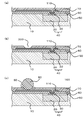
- (First embodiment) 1 to 3 are views for explaining an example of a method for manufacturing the semiconductor device 100 according to the present embodiment.
- the manufacturing method of the semiconductor device 100 according to the present embodiment includes a plurality of semiconductor chips 40 having connection terminals 30 on the surface. And a step of forming a first insulating resin film 60 in a region on the surface of the structure on the side where the connection terminals 30 of the semiconductor chip 40 are embedded. Forming a first opening 250 exposing a part of the connection terminal 30 in the first insulating resin film 60 and the structure; the exposed connection terminal 30; and the first insulating resin film.
- the second opening 300 is formed outside the region formed on the semiconductor chip 40 in the second insulating resin film 70. It is characterized by forming.
- a resin material constituting the first insulating resin film 60 a photosensitive resin composition containing an alkali-soluble resin, and about droplets made of such a photosensitive resin composition. It is particularly important to use a droplet whose surface tension measured by the hanging drop method is 20 mN / m or more and 45 mN / m or less.
- the manufacturing method according to the present embodiment is a method characterized in that the semiconductor chip 40 is sealed from the surface of the semiconductor chip 40 opposite to the side on which the electrode pads 30 are disposed.
- a plurality of semiconductor chips 40 obtained by separating a semiconductor wafer that has been passivated in advance by forming a passivation film 50 are separated at predetermined intervals.
- a structure in which the terminal surface of the semiconductor chip 40 (the surface on which the electrode pad 30 is disposed) is attached to the adhesive surface of the adhesive member 200 is prepared.
- a method for manufacturing such a structure a method of dividing the semiconductor wafer into a state in which the semiconductor wafer is attached to the adhesive surface of the adhesive member 200 may be used.
- a method of die-bonding the semiconductor chip 40 to the adhesive surface of the adhesive member 200 may be used.
- the photosensitive resin composition used in order to form the 1st insulating resin film 60 mentioned later can be used as a material which forms the said passivation film 50.
- the plurality of semiconductor chips 40 are embedded in the sealing material 10 so that the electrode pads 30 provided on the respective surfaces all face the same direction. It is preferable.
- a pillar-shaped conductor portion made of a metal such as copper may be formed on the electrode pad 30 provided in the semiconductor chip 40 described above.
- solder bumps may be formed on the end surface of the conductor portion opposite to the side where the electrode pads are disposed.
- the plurality of semiconductor chips 40 attached to the adhesive member 200 are covered and sealed with a cured product of the semiconductor sealing resin composition.
- cured material of the resin composition for semiconductor sealing shows a sealing material.
- known materials can be used, and examples thereof include an epoxy resin composition containing an epoxy resin, an inorganic filler, and a curing agent.
- examples of the method for sealing the semiconductor chip 40 using the semiconductor sealing resin composition include a transfer molding method, a compression molding method, an injection molding method, and a lamination method.
- a transfer molding method, a compression molding method, or a lamination method is preferable from the viewpoint of forming the sealing material 10 without leaving an unfilled portion. Therefore, it is preferable that the resin composition for semiconductor sealing used for this manufacturing method is a granular form, a granular form, a tablet form, or a sheet form.
- the compression molding method is particularly preferable from the viewpoint of suppressing the occurrence of displacement of the semiconductor chip 40 during the molding of the sealing material 10.
- the adhesive member 200 is peeled off. By doing so, it is possible to obtain a structure in which a plurality of semiconductor chips 40 having electrode pads 30 on the surface are embedded in the sealing material 10.
- the adhesive member 200 is preferably peeled off from the structure after reducing the adhesion between the adhesive member 200 and the structure.
- the adhesion layer between the adhesive member 200 and the structure is adhered by, for example, performing ultraviolet irradiation or heat treatment to deteriorate the adhesion layer of the adhesion member 200 forming the adhesion site. A method of reducing the property.
- the adhesive member 200 is not particularly limited as long as it adheres to the semiconductor chip 40, and examples thereof include a member in which a back grind tape and an adhesive layer are laminated.
- the structure shown in FIG. 1C relates to an aspect in which the surface of the semiconductor chip 40 opposite to the side on which the electrode pads 30 are disposed is covered with the sealing material 10.
- the sealing material 10 is a known method so that the surface of the semiconductor chip 40 opposite to the side on which the electrode pad 30 is disposed is exposed. The step of polishing and removing may be included.
- a first insulating resin film 60 is formed on the surface of the obtained structure on the side where the electrode pad 30 is embedded.
- the first insulating resin film 60 is formed by applying and drying a varnish-like resin composition on the surface of the structure body on which the electrode pad 30 is embedded. To do.
- the film thickness of the first insulating resin film 60 can be, for example, 5 ⁇ m or more and 300 ⁇ m or less.
- a known method such as a spin coating method, a slit coating method, an ink jet method, or the like can be employed. Among these, a spin coating method is preferably employed.
- the photosensitive resin composition containing alkali-soluble resin as a resin material which comprises the 1st insulating resin film 60 Comprising: It consists of this photosensitive resin composition. It is important to use a droplet whose surface tension measured by the hanging drop method is 20 mN / m or more and 45 mN / m or less. Thus, the first insulating resin film 60 having excellent shape reliability can be formed on the sealing material 10 with a high yield. Moreover, the detail of the photosensitive resin composition used for this manufacturing method is mentioned later.
- the present manufacturing method it is preferable to perform plasma treatment on the surface of the sealing material 10 on the side where the first insulating resin film 60 is formed before the first insulating resin film 60 is formed. .
- the wettability of the first insulating resin film 60 can be improved.
- the adhesion between the sealing material 10 and the first insulating resin film 60 is further improved.
- argon gas, oxidizing gas, or fluorine-based gas can be used as a processing gas.
- the oxidizing gas include O 2 gas, O 3 gas, CO gas, CO 2 gas, NO gas, and NO 2 gas.
- an oxidizing gas is preferably used as the processing gas.
- the oxidizing gas for example, O 2 gas is preferably used.
- O 2 gas is preferably used as the oxidizing gas.
- a specific functional group can be formed on the surface of the sealing material 10. Therefore, the adhesion and applicability of the first insulating resin film 60 to the sealing material 10 can be further improved, and the reliability of the semiconductor device can be further improved.
- the conditions for the plasma treatment in this production method are not particularly limited, but in addition to the ashing treatment, a treatment for contacting with plasma derived from an inert gas may be used.
- the plasma processing which concerns on this manufacturing method is the plasma processing performed without applying a bias voltage to a process target, or the plasma processing performed using non-reactive gas.
- it may replace with the plasma processing mentioned above, may implement a chemical
- medical solution process alkaline permanganate aqueous solution, such as potassium permanganate and sodium permanganate, is mentioned, for example.
- a first opening 250 that exposes a part of the electrode pad 30 is formed in the first insulating resin film 60.
- a method of forming the first opening 250 an exposure development method or a laser processing method can be used.
- the desmear process which removes the smear produced when forming this 1st opening part 250 about the formed 1st opening part 250.
- FIG. This desmear processing method can be performed by the following method, for example. First, the structure having the first insulating resin film 60 in which the first opening 250 is formed is immersed in a swelling liquid containing an organic solvent, and then immersed in an alkaline permanganate aqueous solution.
- the permanganate examples include potassium permanganate and sodium permanganate.
- the temperature of the potassium permanganate aqueous solution to be immersed is preferably 45 ° C. or higher, and preferably 95 ° C. or lower.
- the immersion time in the aqueous potassium permanganate solution is preferably 2 minutes or more, and preferably 20 minutes or less. By doing so, the adhesion between the first insulating resin film 60 and the sealing material 10 can be improved more reliably.
- argon gas, O 2 gas, O 3 gas, CO gas, CO 2 gas, NO gas, NO 2 gas, or fluorine-based gas can be used as the processing gas.
- a conductive film 110 is formed so as to cover the exposed electrode pad 30 and the first insulating resin film 60.
- the conductive film 110 is, for example, a solder plating film, a tin plating film, a two-layer plating film in which a gold plating film is laminated on a nickel plating film, or an under bump metal (UBM) film formed by electroless plating. It can be.
- the film thickness of the electrically conductive film 110 can be 2 micrometers or more and 10 micrometers or less, for example. And about the obtained electrically conductive film 110, you may plasma-process with the method similar to the method mentioned above from the viewpoint of improving the durability of the semiconductor device 100 finally obtained.
- the conductive film 110 can be formed as follows. Note that although an example in which the conductive film 110 including two layers of nickel and gold is formed is described here, the present invention is not limited to this.
- a nickel plating film is formed.
- the structure shown in FIG. 2B is immersed in a plating solution.
- the conductive film 110 can be formed on the electrode pad 30 and the surface of the first insulating resin film 60.
- the plating solution nickel lead and a reducing agent containing, for example, hypophosphite can be used.
- electroless gold plating is performed on the nickel plating film.
- the method of electroless gold plating is not particularly limited, for example, it can be performed by substitution gold plating performed by substitution of gold ions and ions of a base metal.
- a second insulating resin film 70 is formed on the surface of the conductive film 110.
- the second opening 300 that exposes a part of the conductive film 110 is formed outside the region formed on the semiconductor chip 40 in the second insulating resin film 70.
- the method for forming the second insulating resin film 70 and the second opening 300 is the same as the method for forming the first insulating resin film 60 and the first opening 250. it can.
- a photosensitive resin composition used for forming the first insulating resin film 60 can be used as a material for forming the second insulating resin film 70.
- the solder bump 80 or the end portion of the bonding wire is melted and fused onto the conductive film 110 exposed in the second opening 300.
- the semiconductor device 100 according to the present embodiment can be obtained.
- the semiconductor device 100 may be divided into a plurality of semiconductor packages by cutting along the dicing line formed in the semiconductor device 100 so as to include at least one semiconductor chip 40. it can.
- a semiconductor having a multilayer wiring structure in which a conductive film (wiring layer) and an insulating resin film are stacked in this order starting from the structure shown in FIG. Devices can also be made.
- a semiconductor device including a four-layer conductive film (wiring layer) and a five-layer insulating resin film can be manufactured.
- a method for forming the conductive film (wiring layer) a method similar to the method for forming the conductive film 110 can be used.
- the insulating resin film can be formed using the same method as the first insulating resin film 60.
- the solder bump 80 or the end of the bonding wire is melted to the outermost layer and melted to the conductive film (wiring layer) by the same method as described above. By attaching, the obtained semiconductor device can be electrically connected.
- the manufacturing method described above relates to a method of forming an insulating resin film and a conductive film (wiring layer) only on one surface of the structure starting from the structure shown in FIG.
- the structure shown in FIG. 1C is in a state where the surface of the semiconductor chip 40 opposite to the side on which the electrode pads 30 are disposed is also exposed, the structure is insulated from both surfaces of the structure.
- a conductive resin film may be formed.
- the manufacturing method can also be applied to a process for manufacturing a chip-sized semiconductor package. From the viewpoint of improving the productivity of a semiconductor package, the process for manufacturing the wafer level package described above in the background section. Or, it is preferably applied to a process for producing a panel level package on the premise that a large area panel larger than the wafer size is used.
- the manufacturing method according to the present embodiment is a method characterized in that the semiconductor chip 40 is sealed from the surface of the semiconductor chip 40 on the side where the electrode pads 30 are disposed. And different. However, also in the manufacturing method according to the present embodiment, a semiconductor device having excellent adhesion between the sealing material 10 and the first insulating resin film 60 can be obtained, as in the first embodiment. The effect of.
- This manufacturing method will be described with reference to FIGS. 4 to 5 are diagrams for explaining an example of a method for manufacturing the semiconductor device 100 according to the present embodiment.
- a support 500 having a release film disposed on one surface of a base substrate is prepared.
- the base substrate include a panel, a wafer, a glass substrate, and a stainless plate.
- the semiconductor chip 40 in which the metal pillar 130 is formed on the electrode pad 30 is disposed on the release film of the support 500 described above. At this time, the semiconductor chip 40 is disposed on the support 500 such that the electrode pad 30 provided in the semiconductor chip 40 faces the surface opposite to the surface on which the support 500 is disposed.
- the semiconductor chip 40 is sealed from the surface of the semiconductor chip 40 on the side where the electrode pads 30 are disposed, using a semiconductor sealing resin composition.
- the sealing material 10 is polished and removed so that the surface of the metal pillar 130 formed on the electrode pad 30 in the semiconductor chip 40 is exposed.
- the support 500 is separated and selectively removed.
- the semiconductor chip 40, the electrode pad 30, and the metal pillar 130 are embedded in the sealing material 10, and the side opposite to the surface on which the electrode pad 30 is disposed in the metal pillar 130. It is possible to obtain a structure in which the surface is exposed.
- the support 500 is preferably peeled after reducing the adhesion between the support 500 and the sealing material 10.
- the material forming the adhesion site in the support 500 is deteriorated by, for example, performing ultraviolet irradiation or heat treatment on the adhesion site between the support 500 and the sealing material 10. It is preferable to peel after reducing the adhesion.
- the selective removal described above refers to removing a part or all of the support 500.
- Methods such as a chemical etching method using an acidic liquid or an alkaline liquid, a physical polishing method, a physical peeling method, a plasma irradiation method, a laser ablation method, and the like can be employed. Among them, a method of chemically removing with an acidic solution or an alkaline solution is preferable. Specific examples of the acidic solution used at this time include mixed acids and aqueous ferric chloride solutions.
- the timing of peeling the support 500 is not limited to the timing described above with reference to FIG. 4D, and may be after the semiconductor device 100 shown in FIG. 5 is manufactured.
- the semiconductor device 100 shown in FIG. 5 can be obtained.
- the photosensitive resin composition used in this manufacturing method is used to form permanent films such as the first insulating resin film 60, the second insulating resin film 70, and the passivation film 50, for example.
- the cured film which comprises a permanent film will be obtained by hardening the photosensitive resin composition.
- a resin film obtained by applying a photosensitive resin composition is patterned into a desired shape by exposure and development, and then the permanent film is formed by curing the resin film by heat treatment or the like. .
- the photosensitive resin composition used for this manufacturing method contains alkali-soluble resin. And the photosensitive resin composition used for this manufacturing method was controlled so that the surface tension of the droplet made of the photosensitive resin composition measured by the hanging drop method was 20 mN / m or more and 45 mN / m or less. Need to be. By carrying out like this, the wettability with respect to the sealing material 10 of the photosensitive resin composition used in order to form the 1st insulating resin film 60 can be improved. Therefore, according to this manufacturing method, when the first insulating resin film 60 is formed by using the photosensitive resin composition in which the surface tension of the droplets is within the above numerical range, It is possible to effectively suppress the occurrence of inconvenience due to coating unevenness of the conductive resin composition.
- the first insulating resin film 60 excellent in reliability is formed on the sealing material 10 by using the photosensitive resin composition in which the surface tension of the droplet is within the above numerical range.
- the photosensitive resin composition used for this manufacturing method compared with the conventional resin material, the familiarity (applicability
- the photosensitive resin composition having a surface tension within the above numerical range it is excellent in reliability from the viewpoint of suppressing inconvenience caused by uneven coating of the photosensitive resin composition such as repelling. Further, the first insulating resin film 60 can be manufactured with a high yield. Thereby, in the case where the shear stress generated by the difference in linear expansion coefficient between the materials forming the first insulating resin film 60 and the sealing material 10 that is the adherend is applied. However, as a result, it is possible to prevent peeling or cracking from occurring at the bonding interface. Specifically, by using a photosensitive resin composition having a surface tension within the above numerical range, the peeling durability at the bonding interface between the first insulating resin film 60 and the sealing material 10 that is the adherend is used. Can be improved to such an extent that it can withstand the shear stress.
- the lower limit of the surface tension of the droplet made of the photosensitive resin composition used in the present production method measured by the hanging drop method is 20 mN / m or more, preferably 25 mN / m. That's it.
- the adhesive strength adheresiveness
- handling properties can be improved.
- the upper limit value of the surface tension of the droplet made of the photosensitive resin composition used in the present production method measured by the hanging drop method is 45 mN / m or less, as described above, but 42 mN / m or less. Is preferable, and it is more preferable that it is 40 mN / m or less.
- the first insulating resin film 60 excellent in reliability can be manufactured with high yield.
- a cured product having a thickness of 10 mm ⁇ 60 mm ⁇ 10 ⁇ m obtained by heat-treating the photosensitive resin composition used in the present production method at 230 ° C. for 90 minutes was used as a test piece, and the stretch rate was 5 mm at 23 ° C.
- the tensile elongation rate of the test piece is preferably 20% or more and 200% or more, more preferably 25% or more and 200% when a tensile test is performed by a method based on JIS K7161 under the conditions of / min. That's it. By doing so, it is possible to form the first insulating resin film 60 having excellent durability that is not easily affected by the interface stress acting on the bonding interface with the sealing material 10, and as a result, peeling, cracking, etc. Can be prevented from occurring.
- the glass transition temperature of the cured product obtained by heat-treating the photosensitive resin composition used in this production method under the conditions of 230 ° C. and 90 minutes is preferably 180 ° C. or more, and more preferably, 200 ° C. or higher.
- the upper limit of the glass transition temperature is sufficient if it is about 300 ° C. or lower.
- a cured product having a thickness of 10 mm ⁇ 60 mm ⁇ 10 ⁇ m obtained by heat-treating the photosensitive resin composition used in the present production method at 230 ° C. for 90 minutes was used as a test piece, and the stretch rate was 5 mm at 23 ° C.
- the tensile elastic modulus of the test piece when a tensile test is performed by a method based on JIS K7161 under the conditions of / min is preferably 2 GPa or more and 5 GPa or less, and more preferably 2.5 GPa or more and 4 GPa or less. is there. By doing so, it is possible to form the first insulating resin film 60 having excellent durability that is not easily affected by the interface stress acting on the bonding interface with the sealing material 10, and as a result, peeling, cracking, etc. Can be prevented from occurring.
- the curing temperature of the photosensitive resin composition used in this production method is preferably 150 ° C. or higher and 250 ° C. or lower, and more preferably 160 ° C. or higher and 230 ° C. or lower.
- the method of preparing the photosensitive resin composition and the measurement by the hanging drop method by appropriately selecting the type and mixing ratio of each raw material component constituting the photosensitive resin composition. It becomes possible to make the value of the surface tension within a desired range. Specifically, a specific alkali-soluble resin, which will be described later, is dissolved in a specific solvent, and further, the type and content of each component such as a crosslinking agent, a silane coupling agent, a dissolution accelerator, and a surfactant are appropriately set. It is preferable to control. As a method for preparing the photosensitive resin composition, for example, it is considered to be important to mix each component in a nitrogen atmosphere. However, the preparation method of the photosensitive resin composition which concerns on this embodiment is not limited to these.
- the inventors have controlled the surface tension of the droplets made of the photosensitive resin composition within a specific numerical range, the applicability of the photosensitive resin composition to the sealing material, and the photosensitive resin composition
- a method for improving the adhesion between the cured product and the sealing material and further improving the reliability of the semiconductor device was studied.
- an alkali-soluble resin having a specific structural unit is dissolved in a specific solvent, and the dispersibility of the alkali-soluble resin is further increased by additives such as a crosslinking agent, a silane coupling agent, a dissolution accelerator, and a surfactant. I found it important to improve.
- the insulating resin film in order to improve mechanical properties such as tensile elongation and tensile modulus of the insulating resin film, it is preferable to include, for example, an alkali-soluble resin having a specific structure to be described later.
- an alkali-soluble resin having a specific structure in order to disperse
- a crosslinking agent it is preferable to use 2 or more types in combination, for example. Thereby, the entanglement between the alkali-soluble resins can be appropriately controlled. Thereby, the dispersibility of alkali-soluble resin can be improved.
- silane coupling agent what contains the specific structural unit mentioned later is preferable, for example, Furthermore, it is preferable to combine the alkali-soluble resin of a specific structure, and the silane coupling agent of a specific structure. Moreover, as a solubility promoter, what contains the specific structural unit mentioned later is preferable, for example. Thereby, the compatibility of the raw material components in the photosensitive resin composition can be improved. Furthermore, it is preferable to use what has a specific functional group mentioned later as surfactant, for example. By appropriately controlling the above elements, it is possible to control the surface tension of the droplet made of the photosensitive resin composition within an appropriate numerical range.
- the photosensitive resin composition contains an alkali-soluble resin as described above.
- the photosensitive resin composition preferably contains a photosensitive agent from the viewpoint of enabling a coating film obtained by applying the photosensitive resin composition to be patterned by lithography. .
- a photosensitive agent from the viewpoint of enabling a coating film obtained by applying the photosensitive resin composition to be patterned by lithography.
- alkali-soluble resin Specific examples of alkali-soluble resins include phenolic resins, hydroxystyrene resins (polyhydroxystyrene), (meth) acrylic acid resins, acrylic resins such as (meth) acrylic ester resins, polybenzoxazole precursors and polyimide precursors, etc.
- the developability, curability, adhesion and film formability of the photosensitive resin composition, the mechanical strength and heat resistance of the cured film obtained by curing the resin film, and the adhesion to other members are improved.
- a precursor having an amide bond having a repeating unit represented by the following general formula (1) is particularly preferable.
- the polybenzoxazole precursor and the polyimide precursor are a kind of polyamide resin and have an amide bond.
- X and Y are organic groups.
- R 1 is a hydroxyl group, —O—R 3 , an alkyl group, an acyloxy group, or a cycloalkyl group, and when there are a plurality of R 1 s , they may be the same or different.
- R 2 is a hydroxyl group, a carboxyl group, —O—R 3 , or —COO—R 3 , and when there are a plurality of R 2 s , they may be the same or different.
- R 3 in R 1 and R 2 is an organic group having 1 to 15 carbon atoms. When R 1 has no hydroxyl group, at least one of R 2 is a carboxyl group.
- R 1 is a hydroxyl group.
- m is an integer from 0 to 8
- n is an integer from 0 to 8.
- X, Y, R 1 to R 3 , m and n may be the same for each repeating unit, or may be different from each other.
- a polyimide resin or a polybenzoxazole resin, or an imide bond and an oxazole ring are generated by causing a heat dehydration or a dehydration reaction using a catalyst.
- a copolymer is produced.
- the alkali-soluble resin may further contain one or both of a polyimide resin and a polybenzoxazole resin.
- the precursor having an amide bond represented by the formula (1) is a polybenzoxazole precursor
- at least one of R 1 is a hydroxyl group.
- a dehydration ring closure occurs between R 1 and the amide structure by heat dehydration or a dehydration reaction using a catalyst, and a polybenzoxazole resin having an oxazole ring is generated.
- the alkali-soluble resin contains at least one of a polybenzoxazole precursor or a polybenzoxazole resin.
- the precursor having an amide bond represented by the formula (1) is a polyimide precursor
- at least one of R 2 is a carboxyl group.
- dehydration ring closure occurs between R 2 and the amide structure by heat dehydration or a dehydration reaction using a catalyst, and a polyimide resin is generated.
- the alkali-soluble resin contains at least one of a polyimide precursor or a polyimide resin.
- Examples of the organic group as X of the precursor having an amide bond having the structure represented by the formula (1) include an aromatic group having a structure such as a benzene ring, a naphthalene ring or a bisphenol structure, a pyrrole ring or a furan ring. And a heterocyclic organic group having the structure: and a siloxane group.
- X in the precursor having an amide bond having a structure represented by the formula (1) is an organic group.
- X for example, those containing an aromatic ring in the structural unit are preferable.
- the aromatic ring refers to a benzene ring; a condensed aromatic ring such as a naphthalene ring, an anthracene ring, or a pyrene ring; a heteroaromatic ring such as a pyridine ring or a pyrrole ring.
- Y in the precursor having an amide bond having a structure represented by the formula (1) is an organic group, and examples of such an organic group include the same as X.
- Y in the formula (1) is, for example, an aromatic group having a structure such as a benzene ring, a naphthalene ring or a bisphenol structure, a heterocyclic organic group having a structure such as a pyrrole ring, a pyridine ring or a furan ring, and a siloxane group. Is mentioned.
- Y in the precursor having an amide bond having a structure represented by the formula (1) is an organic group.
- Y what contains an aromatic ring in the structural unit is preferable, for example.
- mechanical properties such as glass transition temperature, tensile elongation, and tensile elastic modulus of the insulating resin film can be improved, and the reliability of the semiconductor device can be improved.
- both X and Y contain an aromatic ring.
- the molecular chains of the precursor can easily interact with each other, mechanical properties such as glass transition temperature, tensile elongation, and tensile elastic modulus of the insulating resin film can be further improved, and the reliability of the semiconductor device can be further improved.
- the terminal amino group of the precursor is converted to an alkenyl group, an alkynyl group, and the like so as not to affect the mechanical properties and heat resistance of the cured product.
- the end-capping can also be carried out as an amide using an acid anhydride or monocarboxylic acid containing an aliphatic group or a cyclic compound group having at least one organic group selected from hydroxyl groups.
- the precursor having an amide bond represented by formula (1) may have a group in which at least one end of the precursor is end-capped with a nitrogen-containing cyclic compound. Thereby, adhesiveness with a metal wiring (especially copper wiring) etc. can be improved.
- acid anhydrides or monocarboxylic acids containing an aliphatic group or cyclic compound group having at least one organic group selected from alkenyl groups, alkynyl groups, and hydroxyl groups include maleic anhydride, citraconic anhydride, and the like.
- 2,3-dimethylmaleic anhydride 4-cyclohexene-1,2-dicarboxylic anhydride, exo-3,6-epoxy-1,2,3,6-tetrahydrophthalic anhydride, 5-norbornene -2,3-dicarboxylic anhydride, methyl-5-norbornene-2,3-dicarboxylic anhydride, itaconic anhydride, het acid anhydride, 5-norbornene-2-carboxylic acid, 4-ethynylphthalic anhydride , 4-phenylethynylphthalic anhydride, 4-hydroxyphthalic anhydride, 4-hydroxybenzoic acid, and 3-hydroxybenzoic acid It can be mentioned. These may be used alone or in combination of two or more, and a part of the end-capped amide moiety may be dehydrated and closed.
- a precursor having an amide bond represented by formula (1) at least one organic group selected from an alkenyl group, an alkynyl group, and a hydroxyl group is used as the terminal carboxylic acid residue of the precursor.
- An amine derivative containing a group of aliphatic groups or cyclic compound groups can be used to end-cleave as an amide.
- a group end-capped with a nitrogen-containing cyclic compound is added to at least one of the ends to such an extent that the mechanical properties and heat resistance of the cured product are not affected. You may have. Thereby, adhesiveness with a metal wiring (especially copper wiring) etc. can be improved.
- the nitrogen-containing cyclic compound include 1- (5-1H-triazoyl) methylamino group, 3- (1H-pyrazoyl) amino group, 4- (1H-pyrazoyl) amino group, and 5- (1H-pyrazoyl) amino group.
- the precursor having an amide bond represented by the formula (1) is selected from, for example, diamine, bis (aminophenol) or diaminophenol having a structure containing a group represented by X in the formula (1).
- a dicarboxylic acid to obtain a precursor having an amide bond represented by the formula (1)
- 1-hydroxy-1,2,3-benzotriazole or the like is used to increase the reaction yield.
- a dicarboxylic acid derivative of the active ester type reacted in advance may be used.
- the precursor having an amide bond represented by the formula (1) is heated at, for example, 300 to 400 ° C., the precursor is dehydrated and closed, and as a result, polyimide, polybenzoxazole, or both A resin having excellent heat resistance can be obtained in the form of a copolymer.
- the precursor having an amide bond represented by the formula (1) is a polybenzoxazole precursor
- at least one of R 1 in the formula (1) is a hydroxyl group.
- a dehydration ring closure occurs between R 1 and the amide structure by heat dehydration or a dehydration reaction using a catalyst, and a polybenzoxazole resin having an oxazole ring is generated.
- the alkali-soluble resin contains at least one of a polybenzoxazole precursor or a polybenzoxazole resin.
- the precursor having an amide bond represented by the formula (1) is a polyimide precursor
- at least one of R 2 in formula (1) is a carboxyl group.
- dehydration ring closure occurs between R 2 and the amide structure by heat dehydration or a dehydration reaction using a catalyst, and a polyimide resin is generated.
- the alkali-soluble resin contains at least one of a polyimide precursor or a polyimide resin.
- the phenol resin in the alkali-soluble resin examples include a reaction product of a phenol compound typified by a novolak type phenol resin and an aldehyde compound, or a reaction product of a phenol compound typified by a phenol aralkyl resin and a dimethanol compound or a derivative thereof. Can be used. Among these, it is particularly preferable to use a phenol resin obtained by reacting a phenol compound with an aldehyde compound from the viewpoint of suppressing film loss in the development process, improving thermal stability, and manufacturing cost.
- phenol compounds include cresols such as phenol, o-cresol, m-cresol or p-cresol, 2,3-xylenol, 2,4-xylenol, 2,5-xylenol, 2,6-xylenol, 3, Xylenols such as 4-xylenol or 3,5-xylenol, ethylphenols such as o-ethylphenol, m-ethylphenol or p-ethylphenol, alkylphenols such as isopropylphenol, butylphenol or p-tert-butylphenol, or Polyhydric phenols such as resorcin, catechol, hydroquinone, pyrogallol or phloroglucin can be used. These phenol compounds can be used alone or in combination of two or more.
- the aldehyde compound is not particularly limited as long as it is an organic group having an aldehyde group.
- formalin, paraformaldehyde, acetaldehyde, benzaldehyde, or salicylaldehyde can be used.
- the benzaldehyde one substituted with at least one of an alkyl group, an alkoxy group or a hydroxy group, or an unsubstituted one can be used.
- These aldehyde compounds can be used alone or in combination of two or more.
- a phenol resin that is an alkali-soluble resin is obtained by synthesizing the phenol compound and the aldehyde compound by reacting them under an acid catalyst.
- the acid catalyst is not particularly limited, and for example, oxalic acid, nitric acid, sulfuric acid, diethyl sulfate, acetic acid, p-toluenesulfonic acid, phenolsulfonic acid, or benzenesulfonic acid can be used.
- dimethanol compound examples include 1,4-benzenedimethanol, 1,3-benzenedimethanol, 4,4′-biphenyldimethanol, 3,4′-biphenyldimethanol, 3,3′-biphenyldimethanol, or Dimethanol compounds such as 2,6-naphthalenediethanol, 1,4-bis (methoxymethyl) benzene, 1,3-bis (methoxymethyl) benzene, 4,4′-bis (methoxymethyl) biphenyl, 3,4 Bis (alkoxymethyl) compounds such as' -bis (methoxymethyl) biphenyl, 3,3'-bis (methoxymethyl) biphenyl or methyl 2,6-naphthalenedicarboxylate, or 1,4-bis (chloromethyl) benzene, 1,3-bis (chloromethyl) benzene, 1,4-bis (bromomethyl) benzene, 1, -Bis (bromomethyl) benzene, 4,4'-bis (chloromethyl)
- hydroxystyrene resin in the alkali-soluble resin a polymerization reaction product or a copolymerization reaction product obtained by radical polymerization, cation polymerization, or anion polymerization of hydroxystyrene, styrene, or a derivative thereof can be used.
- the phenol resin in the alkali-soluble resin examples include a reaction product of a phenol compound typified by a novolak type phenol resin and an aldehyde compound, or a reaction product of a phenol compound typified by a phenol aralkyl resin and a dimethanol compound or a derivative thereof. Can be used. Among these, it is particularly preferable to use a phenol resin obtained by reacting a phenol compound with an aldehyde compound from the viewpoint of suppressing film loss in the development process, improving thermal stability, and manufacturing cost.
- the alkali-soluble resin is a polymer of a cyclic olefin monomer such as norbornene or cycloalkane (cyclic olefin-based resin)
- examples of the polymerization method of the polymer include an addition polymerization method and a ring-opening polymerization method. These polymers may be random copolymers, block copolymers, or alternating copolymers.
- cyclic olefin monomer examples include monocyclic compounds such as cyclohexene and cyclooctene, norbornene, norbornadiene, dicyclopentadiene, dihydrodicyclopentadiene, tetracyclododecene, tricyclopentadiene, dihydrotricyclopentadiene, tetra And polycyclic compounds such as cyclopentadiene and dihydrotetracyclopentadiene.
- bonded with these monomers can also be used as a cyclic olefin monomer which concerns on this embodiment.
- the cyclic olefin resin according to the present embodiment is preferably a norbornene resin from the viewpoint of heat resistance.
- the norbornene-based resin described above is, for example, ring-opening metathesis polymerization (ROMP), a combination of ROMP and a hydrogenation reaction, polymerization using radicals or cations, polymerization using a cationic palladium polymerization initiator, and other polymerization initiation. It can be obtained by all known polymerization methods such as polymerization using an agent (for example, polymerization initiator of nickel or other transition metal).
- the cyclic olefin resin according to the present embodiment is an addition polymer of a cyclic olefin monomer
- specific examples of the addition polymer include those shown in the following (1) to (3).
- (1) Addition (co) polymer of norbornene type monomer obtained by addition (co) polymerization of norbornene type monomer.
- (2) An addition copolymer of a norbornene type monomer and ethylene or ⁇ -olefins.
- An addition polymer such as an addition copolymer of a norbornene-type monomer and a non-conjugated diene and, if necessary, another monomer.
- the above addition polymer can be obtained by coordination polymerization using a metal catalyst or radical polymerization.
- a polymer in coordination polymerization, can be obtained by polymerizing a monomer in a solution in the presence of a transition metal catalyst.
- metal catalysts used for coordination polymerization include (toluene) bis (perfluorophenyl) nickel, (mesylene) bis (perfluorophenyl) nickel, (benzene) bis (perfluorophenyl) nickel, bis (tetrahydro) bis Known metal catalysts such as (perfluorophenyl) nickel, bis (ethyl acetate) bis (perfluorophenyl) nickel, and bis (dioxane) bis (perfluorophenyl) nickel may be mentioned.
- the cyclic olefin-based resin according to the present embodiment is a ring-opening polymer of a cyclic olefin monomer
- specific examples of the ring-opening polymer include the following (4) to (6).
- a ring-opening copolymer of a norbornene-type monomer and a non-conjugated diene or other monomer is produced by ring-opening (co) polymerization of at least one or more norbornene-type monomers by a known ring-opening polymerization method using titanium or a tungsten compound as a catalyst. Then, if necessary, the carbon-carbon double bond in the ring-opening (co) polymer is hydrogenated by a conventional hydrogenation method to produce a thermoplastic saturated norbornene resin.
- the norbornene-based resin may be a ring-opening polymer such as a polymer obtained by hydrogenating the (co) polymer shown in the above (1) to (6) as necessary.
- the content of the alkali-soluble resin is preferably 10% by weight or more and 70% by weight or less, more preferably 15% by weight or more and 65% by weight or less, based on the total amount of nonvolatile components of the photosensitive resin composition. More preferably, it is 20 to 50 weight%.
- the curability of the photosensitive resin composition can be improved by setting the content of the alkali-soluble resin to the above lower limit value or more. Thereby, the heat resistance of the permanent film formed using a photosensitive resin composition, mechanical strength, and durability can be improved. On the other hand, the resolution in lithography can be improved by setting the content of the alkali-soluble resin to the upper limit or less.
- the ratio (weight%) of the non-volatile component in the photosensitive resin composition can be measured as follows, for example. First, 1.0 g of the photosensitive resin composition is weighed out as a sample in an aluminum cup whose weight (w 0 ) has been measured. In this case, the total weight of the sample and the aluminum cup and w 1. Next, the aluminum cup is kept in a hot air dryer adjusted to 210 ° C. under normal pressure for 1 hour, and then taken out of the hot air dryer and cooled to room temperature. Next, the total weight (w 2 ) of the cooled sample and the aluminum cup is measured. And the ratio (weight%) of the non-volatile component in the photosensitive resin composition is computed from the following formula
- Formula: Non-volatile content (% by weight) (w 2 ⁇ w 0 ) / (w 1 ⁇ w 0 ) ⁇ 100
- the photosensitive resin composition according to this embodiment may contain a photosensitive agent.
- a photosensitive agent a compound that generates an acid by light, that is, a photoactive compound can be used.
- the photosensitive agent include photosensitive diazoquinone compounds, photosensitive diazonaphthoquinone compounds, diaryliodonium salts, triarylsulfonium salts, onium salts such as sulfonium borate salts, 2-nitrobenzyl ester compounds, N-iminosulfonate compounds, Examples thereof include imidosulfonate compounds, 2,6-bis (trichloromethyl) -1,3,5-triazine compounds, and dihydropyridine compounds.
- a photosensitive diazoquinone compound and a photosensitive diazonaphthoquinone compound that are excellent in sensitivity and solvent solubility are preferable.
- Specific examples thereof include 1,2-benzoquinonediazide-4-sulfonic acid ester of a phenol compound, 1,2-naphthoquinonediazide-4-sulfonic acid ester, 1,2-naphthoquinonediazide-5-sulfonic acid ester, and the like. Can be mentioned.
- the content of the photosensitizer is preferably 1 part by weight or more and 50 parts by weight or less, more preferably 5 parts by weight or more and 40 parts by weight or less, and still more preferably, with respect to 100 parts by weight of the alkali-soluble resin. 8 parts by weight or more and 35 parts by weight or less.
- the photosensitive resin composition according to this embodiment may contain a crosslinking agent.
- a crosslinking agent known compounds can be used as long as they have a group capable of reacting with an alkali-soluble resin.
- Specific examples of the crosslinking agent include epoxy compounds, alkoxymethyl compounds, methylol compounds, oxetane compounds and the like.
- 1 type (s) or 2 or more types can be used in combination in the above specific examples.
- the dispersibility of alkali-soluble resin can be improved because two or more types of crosslinked structures are appropriately entangled.
- mechanical properties such as tensile elongation and tensile modulus of the cured product of the photosensitive resin composition can be further improved.
- the crosslinking agent includes, for example, an alkoxymethyl compound or a methylol compound.
- Specific examples of the methylol compound suitable as the crosslinking agent include paraxylene glycol.
- glycidyl ether such as glycidyl ether, adipic acid diglycidyl ester, glycidyl ester such as o-phthalic acid diglycidyl ester, 3,4-epoxycyclohexylmethyl (3,4-epoxycyclohexane) carboxylate, 3 , 4-Epoxy-6-methylcyclohexylmethyl (3,4-epoxy-6-methylcyclohexane) carboxylate, bis (3,4-epoxy 6-methylcyclohexylmethyl) adipate, dicyclopentanediene oxide, bis (2,3-epoxycyclopentyl) ether, Daicel Corporation's Celoxide 2021, Celoxide 2081, Celoxide 2083, Celoxide 2085, Celoxide 8000, Epoxide GT401, etc.
- LX-01 manufactured by Daiso Corporation
- Poly-functional alicyclic epoxy resins such as Poly [(2-oxylanyl) -1,2-cyclohexandiol] 2-ethyl-2- (hydroxymethyl) -1,3-propanediol ether (3: 1), EHPE- 3150 (manufactured by Daicel Corporation) can also be used.
- the photosensitive resin composition can contain one or more of the epoxy compounds exemplified above.
- crosslinking agent examples include 1,4-bis (methoxymethyl) benzene, 4,4′-biphenyldimethanol, 4,4′-bis (methoxymethyl) biphenyl, manufactured by Honshu Chemical Co., Ltd. TMOM-BP, DML-DP, TMOM-BP-MF, Nicarax MX-270, MX-290, MX-370, etc.
- the content of the crosslinking agent is preferably 1 part by weight or more and 100 parts by weight or less, more preferably 2 parts by weight or more and 50 parts by weight or less with respect to 100 parts by weight of the alkali-soluble resin. Less than parts by weight.
- the content of the crosslinking agent is within the above range, a cured film excellent in chemical resistance and resolution can be formed, which is preferable.
- the photosensitive resin material according to the present embodiment may contain a silane coupling agent.
- a silane coupling agent preferably contain organosilicon.
- the silane coupling agent include 3-glycidoxypropyltrimethoxysilane, 3-glycidoxypropyltriethoxysilane, p-styryltrimethoxysilane, 3-methacryloxypropyltrimethoxysilane, 3-methacrylate.
- Examples thereof include silicon compounds obtained by reacting a silane and a silicon compound having an amino group with an acid dianhydride or an acid anhydride.
- silicon compound having an amino group examples include 3-aminopropyltrimethoxysilane, N- (2-aminoethyl) -3-aminopropyltrimethoxysilane, 3-aminopropylmethyldimethoxysilane, N- (2-aminoethyl) -3-aminopropyltriethoxysilane, 3-aminopropyltriethoxysilane, and the like. These may be used individually by 1 type and may be used in combination of 2 or more type.
- acid dianhydride or acid anhydride examples include maleic anhydride, chloromaleic anhydride, cyanomaleic anhydride, cytoconic acid, phthalic anhydride, pyromellitic anhydride, 4,4′-biphthalate.
- acid dianhydride, 4,4′-oxydiphthalic dianhydride, 4,4′-carbonyldiphthalic anhydride, and the like examples include acid dianhydride, 4,4′-oxydiphthalic dianhydride, 4,4′-carbonyldiphthalic anhydride, and the like. These may be used individually by 1 type and may be used in combination of 2 or more type.
- the silane coupling agent preferably includes, for example, a structural unit represented by the following formula (S1) or formula (S2).
- S1 and S2 a portion where no atomic symbol is described is arbitrary.
- the silane coupling agent having a structure close to that of the polybenzoxazole precursor and the polyimide precursor, the amide bond between the photosensitive resin composition and the sealing material strongly interacts with each other.
- the alkali-soluble resin and the silane coupling agent have an aromatic ring, they interact more strongly by stacking ⁇ electrons.
- the alkali-soluble resin and the silane coupling agent interact with each other, and the silane coupling agent and the sealing material interact with each other, whereby an insulating resin film made of a cured product of the photosensitive resin composition and Adhesiveness with a sealing material can be improved. Further, peeling and cracking are less likely to occur at the interface between the insulating resin film and the sealing material, and the reliability of the semiconductor device can be improved.
- silane coupling agent it is preferable to contain 2 or more types from which the structure differs among the said specific examples, for example, and it is more preferable to contain 3 or more types from which a structure differs. Thereby, the affinity of the photosensitive resin composition with respect to the component contained in the sealing material 10 can be improved. Therefore, the adhesiveness between the cured product of the photosensitive resin composition and the sealing material 10 and the reliability of the semiconductor device can be further improved.
- the silane coupling agent having a different structure preferably contains, for example, one containing a structural unit represented by the above formula (S1) and one containing a structural unit represented by the above formula (S2).
- the content of the silane coupling agent is preferably 0.05 parts by weight or more and 50 parts by weight or less, and more preferably 0.1 parts by weight or more and 20 parts by weight or less with respect to 100 parts by weight of the alkali-soluble resin. More preferably, it is 0.5 parts by weight or more and 10 parts by weight or less.
- the content of the silane coupling agent is within the above range, the preservability of the photosensitive resin composition can be improved and a resin film having excellent adhesion to other members can be formed from the composition. .
- the photosensitive resin composition according to this embodiment may contain a dissolution accelerator.
- the dissolution accelerator is a component capable of improving the solubility of the exposed portion of the coating film formed using the photosensitive resin composition in the developer and improving scum during patterning.
- a dissolution accelerator a compound having a phenolic hydroxyl group is preferable.
- examples of the dissolution accelerator include those having a biphenol type skeleton or bisphenol. Those having an A-type skeleton are preferred. Thereby, the skeleton of the alkali-soluble resin interacts with the dissolution accelerator, and the dispersibility of the alkali-soluble resin can be further improved.
- the dissolution accelerator having a biphenol type skeleton for example, those represented by the following general formula (D1) are preferable, and those having a bisphenol A type skeleton include, for example, the following general formula ( Those represented by D2) are preferred.
- R 3 to R 12 are each independently hydrogen, a hydroxyl group, or an organic group having 1 to 10 carbon atoms, At least one of R 3 to R 7 and at least one of R 8 to R 12 includes a hydroxyl group.
- R 3 to R 12 are each independently hydrogen, a hydroxyl group, or an organic group having 1 to 10 carbon atoms, At least one of R 3 to R 7 and at least one of R 8 to R 12 includes a hydroxyl group.
- R 3 to R 12 in the general formula (D1) and the general formula (D2) are each independently hydrogen, hydroxyl group, or an organic group having 1 to 10 carbon atoms, for example, hydrogen, hydroxyl Group, or an organic group having 1 to 5 carbon atoms, preferably hydrogen, a hydroxyl group, or an organic group having 1 to 3 carbon atoms.
- R 3 to R 12 are monovalent organic groups.
- the monovalent organic group means a valence. That is, each of R 3 to R 12 has one bond that bonds to another atom.
- organic group constituting R 3 to R 12 in the general formulas (D1) and (D2) include a methyl group, an ethyl group, an n-propyl group, an isopropyl group, and an n-butyl group.
- Alkyl groups such as isobutyl, sec-butyl, tert-butyl, pentyl, neopentyl, hexyl, heptyl, octyl, nonyl, decyl; alkenyl such as allyl, pentenyl, vinyl Group; alkynyl group such as ethynyl group; alkylidene group such as methylidene group and ethylidene group; aryl group such as tolyl group, xylyl group, phenyl group, naphthyl group and anthracenyl group; aralkyl group such as benzyl group and phenethyl group; adamantyl group , A cycloalkyl group such as a cyclopentyl group, a cyclohexyl group, a cyclooctyl group; Group, and alkaryl groups, such as xylyl
- At least one of R 3 to R 7 and at least one of R 8 to R 12 includes a hydroxyl group.
- R 5 and R 10 preferably include a hydroxyl group, and R 5 and R 10 are more preferably a hydroxyl group.
- the photosensitive resin composition according to the present embodiment may contain a surfactant.
- the surfactant according to this embodiment includes, for example, a compound containing a fluorine group (for example, a fluorinated alkyl group), a silanol group, or a compound having a siloxane bond as a main skeleton.
- a fluorine group for example, a fluorinated alkyl group
- a silanol group for example, a silanol group
- a compound having a siloxane bond as a main skeleton.
- it is more preferable to use a fluorine-based surfactant or a silicone-based surfactant as the surfactant and it is particularly preferable to use a fluorine-based surfactant.
- a fluorosurfactant examples include Megafac F-171, F-173, F-444, F-470, F-471, F-475, F-482, F-477, manufactured by DIC Corporation. Examples thereof include F-554, F-556 and F-557, Novec FC4430 and FC4432 manufactured by Sumitomo 3M Limited.
- a fluorine-type surfactant shows surfactant provided with a fluorine group.
- a fluorinated surfactant is preferably included.
- the content of the surfactant is preferably 0.005 to 5 parts by weight, more preferably 0.01 to 2 parts by weight, with respect to 100 parts by weight of the alkali-soluble resin. Most preferably, it is 0.01 parts by weight or more and 1 part by weight or less. Thereby, the flatness of the resin film obtained using the photosensitive resin composition can be improved.
- the photosensitive resin composition may contain additives such as a curing agent, an antioxidant, a filler, and a sensitizer in addition to the above-described components as necessary.
- the photosensitive resin composition may contain a solvent.
- the photosensitive resin composition has a varnish shape, for example.
- solvents include N-methyl-2-pyrrolidone, ⁇ -butyrolactone (GBL), N, N-dimethylacetamide, dimethyl sulfoxide, diethylene glycol dimethyl ether, diethylene glycol diethyl ether, diethylene glycol dibutyl ether, propylene glycol monomethyl ether, di- Propylene glycol monomethyl ether, propylene glycol monomethyl ether acetate (PGMEA), methyl lactate, ethyl lactate, butyl lactate, methyl-1,3-butylene glycol acetate, 1,3-butylene glycol-3-monomethyl ether, methyl pyruvate, and Examples include ethyl pyruvate and methyl-3-methoxypropionate.
- the solvent among the above specific examples, for example, those having an ester bond are preferable.
- a solvent provided with an ester bond a heterocyclic compound is preferable, for example.
- the heterocyclic compound for example, those containing a lactone ring are preferred.
- the present inventors examined a combination of an alkali-soluble resin and a solvent. As a result, the alkali-soluble resin containing an aromatic ring in the structural unit had low dispersibility in the solvent. In the conventional photosensitive resin composition having a low dispersibility of the alkali-soluble resin, the surface tension of the droplet made of the photosensitive resin composition does not fall within the specific numerical range described above.
- the applicability of the photosensitive resin composition was low, and a semiconductor device could not be produced. Further, even if the application is made and the semiconductor device is manufactured, there is a disadvantage that the adhesion between the insulating resin film and the sealing material is low and the reliability of the semiconductor device is lowered. Therefore, as a result of studying a solvent that can suitably disperse an alkali-soluble resin containing an aromatic ring in its structural unit, the present inventors have found that the solvent having a specific functional group and structure described above is a dispersion of an alkali-soluble resin. It turned out that it is excellent in property.
- the content of the solvent is, for example, preferably 100 parts by weight or more, and more preferably 130 parts by weight or more with respect to 100 parts by weight of the alkali-soluble resin. Further, the content of the solvent is preferably 300 parts by weight or less, and more preferably 250 parts by weight or less with respect to 100 parts by weight of the alkali-soluble resin, for example. Thereby, workability
- the resin composition for encapsulating a semiconductor according to this embodiment examples include an epoxy resin composition containing a thermosetting resin, an inorganic filler, and a curing agent.
- thermosetting resins include phenol novolak resins, cresol novolak resins, bisphenol A novolak resins, and triazine skeleton-containing phenol novolak resins; unmodified resole phenol resins, tung oil, linseed oil, walnut oil Phenol resins such as resol type phenol resins such as oil-modified resol phenol resin modified with bisphenol A type epoxy resin, bisphenol F type epoxy resin, bisphenol S type epoxy resin, bisphenol E type epoxy resin, bisphenol M type epoxy resin, Bisphenol type epoxy resins such as bisphenol P type epoxy resin and bisphenol Z type epoxy resin; phenol novolac type epoxy resin, cresol novolac type epoxy resin Novolac type epoxy resins such as: biphenyl type epoxy resins, biphenyl aralkyl type epoxy resins, aryl alkylene type epoxy resins, naphthalene type epoxy resins, anthracene type epoxy resins, phenoxy
- the content of the thermosetting resin is preferably 1% by mass or more and 38% by mass or less, and more preferably 1.5% by mass or more and 35% by mass or less with respect to the total amount of the semiconductor sealing resin composition. Yes, more preferably 2% by mass or more and 30% by mass or less, and most preferably 3% by mass or more and 25% by mass or less.
- thermosetting resin it is preferable to use an epoxy resin as the thermosetting resin.
- said epoxy resin it is possible to use the monomer, oligomer, and polymer in general which have 2 or more of epoxy groups in 1 molecule irrespective of the molecular weight and molecular structure.
- epoxy resins include biphenyl type epoxy resins, bisphenol A type epoxy resins, bisphenol F type epoxy resins, stilbene type epoxy resins, hydroquinone type epoxy resins and the like; cresol novolac type epoxy resins, Novolak type epoxy resins such as phenol novolac type epoxy resin and naphthol novolak type epoxy resin; Phenol aralkyl type epoxy such as phenylene skeleton-containing phenol aralkyl type epoxy resin, biphenylene skeleton containing phenol aralkyl type epoxy resin, phenylene skeleton containing naphthol aralkyl type epoxy resin Resin; Trifunctional epoxy resin such as triphenolmethane type epoxy resin and alkyl-modified triphenolmethane type epoxy resin; Examples include modified phenolic epoxy resins such as diene-modified phenolic epoxy resins and terpene-modified phenolic epoxy resins; and heterocyclic-containing epoxy resins such as triazine nucleus-
- a curing agent may be contained in the semiconductor sealing resin composition.
- curing agent should just react and cure with a thermosetting resin.
- specific examples of curing agents that can be used when an epoxy resin is used as the thermosetting resin include linear aliphatic groups having 2 to 20 carbon atoms such as ethylenediamine, trimethylenediamine, tetramethylenediamine, and hexamethylenediamine.
- Aniline Resol type phenol resins such as resole resin and dimethyl ether resole resin; Novolak type phenol resins such as phenol novolak resin, cresol novolak resin, tert-butylphenol novolak resin, non
- Alicyclic acid anhydride trimellitic anhydride (TMA), pyromellitic anhydride (PMDA), benzophenone tetracarboxylic acid
- Acid anhydrides including aromatic acid anhydrides such as BTDA polymercaptan compounds such as polysulfides, thioesters, thioethers
- isocyanate compounds such as isocyanate prepolymers and blocked isocyanates
- organic acids such as carboxylic acid-containing polyester resins, etc. Is mentioned. These may be used alone or in combination of two or more.
- a compound having at least two phenolic hydroxyl groups in one molecule is preferable, and specific examples thereof include phenol novolak resin, cresol novolak resin, tert- Examples thereof include novolak-type phenol resins such as butylphenol novolak resin and nonylphenol novolak resin; resol-type phenol resins; polyoxystyrene such as polyparaoxystyrene; phenylene skeleton-containing phenol aralkyl resins and biphenylene skeleton-containing phenol aralkyl resins.
- the semiconductor sealing resin composition may contain a curing accelerator.
- the curing accelerator is not particularly limited as long as it accelerates the curing reaction between a functional group such as an epoxy group and the curing agent. Specific examples thereof include 1,8-diazabicyclo [5.4.0] undecene- Diazabicycloalkenes and derivatives thereof such as 7; amine compounds such as tributylamine and benzyldimethylamine; imidazole compounds such as 2-methylimidazole; organic phosphines such as triphenylphosphine and methyldiphenylphosphine; tetraphenylphosphonium tetra Phenylborate, Tetraphenylphosphonium ⁇ Tetrabenzoic acid borate, Tetraphenylphosphonium ⁇ Tetranaphthoic acid borate, Tetraphenylphosphonium ⁇ Tetranaphthoyloxyborate, Tetraphenylphosphonium ⁇ Tetranaphthy
- the semiconductor sealing resin composition may contain, if necessary, a silane coupling agent such as ⁇ -glycidoxypropyltrimethoxysilane; a colorant such as carbon black; a natural wax; Mold release agents such as wax, higher fatty acids or metal salts thereof, paraffin wax such as paraffin, paraffin oxide or polyethylene oxide; low stress agents such as silicone oil and silicone rubber; ion scavengers such as hydrotalcite; aluminum hydroxide Flame retardants such as: various additives such as antioxidants may be added.
- a silane coupling agent such as ⁇ -glycidoxypropyltrimethoxysilane
- a colorant such as carbon black
- a natural wax such as wax, higher fatty acids or metal salts thereof, paraffin wax such as paraffin, paraffin oxide or polyethylene oxide
- low stress agents such as silicone oil and silicone rubber
- ion scavengers such as hydrotalcite
- aluminum hydroxide Flame retardants such as: various additives such as antioxidants may
- the resin composition for semiconductor encapsulation contains a release agent such as paraffin wax
- the affinity between the conventional photosensitive resin composition and the resin composition for semiconductor encapsulation is poor and the coating property is inferior.
- the photosensitive resin composition according to the present embodiment has a high affinity with the semiconductor sealing resin composition, it exhibits suitable coating properties even when the semiconductor sealing resin composition contains a release agent. It is convenient from the viewpoint that can be done.
- the resin composition for semiconductor sealing contains a silane coupling agent, for example. Thereby, affinity with the resin composition for sealing and the photosensitive resin composition can be improved, and the applicability
- the encapsulating resin composition preferably contains aminosilane as a silane coupling agent.
- the silane coupling agent contained in the resin composition for sealing and the photosensitive resin composition performs the interaction derived from an amide bond, and can improve applicability
- the pressure-sensitive adhesive member 200 is not particularly limited as long as it can adhere the semiconductor chip 40, but may be formed of a support film and a pressure-sensitive adhesive layer, for example.
- the constituent material of the support film is not particularly limited.
- the surface of the support film can be subjected to chemical or physical surface treatment in order to improve the adhesion with the pressure-sensitive adhesive layer.
- the support film may contain various additives (fillers, plasticizers, antioxidants, flame retardants, antistatic agents) as long as the effects of the invention are not impaired.
- the pressure-sensitive adhesive layer of the pressure-sensitive adhesive member 200 is composed of a first resin composition containing an acrylic pressure-sensitive adhesive, a rubber-based pressure-sensitive adhesive, a vinyl alkyl ether-based pressure-sensitive adhesive, a silicone-based pressure-sensitive adhesive, a polyester-based pressure-sensitive adhesive, and the like. Among them, acrylic pressure-sensitive adhesives are preferable.
- a polyamide resin which is a polybenzoxazole precursor represented by the following formula (2) was obtained as an alkali-soluble resin (A-1).
- the obtained alkali-soluble resin (A-1) had a weight average molecular weight of 17,040.
- the mixed solution was cooled to room temperature, and then the pH was adjusted using a 10 wt% aqueous hydrochloric acid solution so that the pH of the mixed solution was in the range of 6.0 to 7.0.
- the precipitate obtained by filtering out the precipitate deposited in the mixed solution is washed with water, dried at a temperature of 60 to 70 ° C., and bis-N, N ′-(para-nitrobenzoyl) -2. , 2-bis (4-hydroxyphenyl) propane solid was obtained.
- the palladium-carbon catalyst was removed by filtering the suspension, and then the obtained filtrate was subjected to an evaporator to evaporate the solvent component.
- the product thus obtained is dried at 90 ° C., whereby bis-N, N ′-(para-aminobenzoyl) -2,2-bis (4- Hydroxyphenyl) propane was obtained.
- the obtained alkali-soluble resin (A-2) had a weight average molecular weight of 15,200.
- a polyamide resin which is a polybenzoxazole precursor represented by the following formula (6) was obtained as an alkali-soluble resin (A-3).
- the obtained alkali-soluble resin (A-3) had a weight average molecular weight of 17,040.
- the obtained alkali-soluble resin (A-4) had a weight average molecular weight of 9,800.
- each raw material component other than the solvent (G) is dissolved in the solvent (G) in the amount shown in the following Table 1 so that the viscosity after preparation is about 500 mPa ⁇ s. And stirred under a nitrogen atmosphere. Then, the filtrate obtained by filtering with a polyethylene filter having a pore size of 0.2 ⁇ m was obtained as a varnish-like photosensitive resin composition.
- the raw material components of the photosensitive resin composition are shown below.
- Photosensitizer B-1 Photosensitizer (B-1) obtained in Synthesis Example 5 (diazonaphthoquinone compound)
- Thermal crosslinking agent (C) Thermal crosslinking agent C-1: para-xylene glycol (Tokyo Chemical Industry Co., Ltd., (C-1) in the following formula (11))
- Thermal crosslinking agent C-2 Tetramethoxymethylglycoluril (manufactured by Sanwa Chemical Co., Ltd., Nicalak MX-270, (C-2) in the following formula (11))
- Silane coupling agent D-1 3-methacryloxypropyltrimethoxysilane (manufactured by Shin-Etsu Silicone)
- Silane coupling agent D-2 Silane coupling agent obtained by Synthesis Example 6
- Silane coupling agent D-3 Silane coupling agent obtained by Synthesis Example 7
- Surfactant F-1 Fluorosurfactant (manufactured by DIC, MegaFuck F-556)
- Surfactant F-2 Fluorosurfactant (Sumitomo 3M, FC4430)
- Glass transition temperature (Tg) of cured product The obtained varnish-like photosensitive resin compositions according to Examples 1 to 11 and Comparative Example 1 were heat-treated in a nitrogen atmosphere at 230 ° C. for 90 minutes. By curing, a test piece (30 mm ⁇ 5 mm ⁇ 10 ⁇ m thickness) made of a cured product of the photosensitive resin composition was obtained. Subsequently, the thermal expansion coefficient of the test piece obtained at a heating rate of 10 ° C./min was measured using a thermomechanical analyzer (manufactured by Seiko Instruments Inc., TMA / SS6000). Next, based on the obtained measurement results, the glass transition temperature (Tg) of the cured product was calculated from the inflection point of the thermal expansion coefficient. The unit is ° C.
- -Tensile modulus of cured product The obtained varnish-like photosensitive resin compositions according to Examples 1 to 11 and Comparative Example 1 are cured by heat treatment under conditions of 230 ° C and 90 minutes in a nitrogen atmosphere. Thus, a test piece (10 mm ⁇ 60 mm ⁇ 10 ⁇ m thickness) made of a cured product of the photosensitive resin composition was obtained. Next, the obtained test piece was subjected to a tensile test using a tensile tester (Orientec Co., Ltd., Tensilon RTC-1210A) in a 23 ° C. atmosphere according to JIS K7161, and the measurement results obtained. Based on the above, a stress-strain curve was prepared.
- a tensile tester Orientec Co., Ltd., Tensilon RTC-1210A
- the tensile modulus was calculated from the initial gradient of the created stress-strain curve.
- the unit of tensile modulus is GPa.
- the stretching speed in the tensile test was 5 mm / min.
- the evaluation results are shown in Table 1 below.
- the semiconductor device according to each example was manufactured by the following method.
- the film was arranged at 10 mm intervals in the vertical and horizontal directions.
- the simulated element wafer is arranged so that the aluminum circuit faces the surface on the side facing the thermally peelable film in the simulated element wafer.
- the epoxy resin composition comprises a polyfunctional epoxy resin as an epoxy resin, a polyfunctional phenol resin as a curing agent, silica as an inorganic filler, an aminosilane coupling agent as a coupling agent, and a paraffin wax as a release agent. And was included.
- the heat-peelable film is peeled off from the carrier while being heated using a hot plate heated to 200 ° C., and then post-cured at 175 ° C. for 4 hours.
- the encapsulant resin substrate having a built-in semiconductor chip shown in c) (a structure in which a plurality of semiconductor chips are embedded inside the encapsulant, hereinafter also referred to as a chip-embedded encapsulant resin substrate) was obtained.
- first insulating resin film Formation of first insulating resin film
- a batch type plasma processing apparatus manufactured by March
- AP-1000 an oxygen plasma treatment was performed under conditions of an output energy of 800 W, a gas amount of 200 sccm, and a time of 1 minute.
- a pre-bake treatment at 120 ° C.
- an insulating resin film provided with an opening so as to expose a part of the aluminum circuit was prepared by heat-treating and curing at 230 ° C. for 90 minutes in an oxygen atmosphere.
- the chip-embedded sealing material resin substrate provided with the insulating resin film is also referred to as a resin film-equipped sealing material substrate.
- Example 12 the same photosensitive resin composition as in Example 1 was used, and the resin film was cured under an oxygen atmosphere at a temperature of 180 ° C. for 30 minutes to produce an insulating resin film.
- Example 13 the same photosensitive resin composition as in Example 1 was used, and the resin film was cured under an oxygen atmosphere at a temperature of 250 ° C. for 30 minutes to produce an insulating resin film.
- Formation of the second insulating resin film A batch type plasma processing apparatus (manufactured by March) is applied to the surface on the side where the Cu wiring layer is arranged in the sealing material substrate with the Cu wiring layer obtained by the method described above. , AP-1000), and an oxygen plasma treatment was performed under conditions of an output energy of 800 W, a gas amount of 200 sccm, and a time of 1 minute. Next, using a spin coater, the varnish-like photosensitive resin composition produced by the above-described method was applied to the surface of the encapsulant substrate with a Cu wiring layer on which the Cu wiring layer was disposed. Thereafter, a pre-bake treatment was performed at 120 ° C.
- the exposed portion was dissolved and removed by performing paddle development processing twice while adjusting, and then rinsed with pure water for 10 seconds. Thereafter, an insulating resin film provided with an opening so as to expose a part of the Cu wiring layer is produced by heat-treating under an oxygen atmosphere at 230 ° C. for 90 minutes to form a desired semiconductor. Got the device.
- size of 35 mm x 35 mmx300 micrometer thickness was produced by the method similar to the method mentioned above.
- a batch type plasma processing apparatus manufactured by March, AP-1000 is used for the surface on the side where the semiconductor chip is arranged in the obtained semiconductor chip embedded sealing resin substrate, the output energy is 800 W, Oxygen plasma treatment was performed under conditions of a gas amount of 200 sccm and a time of 1 minute.
- the first to third embodiments manufactured by the above-described method so that the film thickness becomes 10 ⁇ m with respect to the surface on the side where the semiconductor chip is disposed in the semiconductor chip embedded sealing resin substrate. 13.
- a varnish-like photosensitive resin composition according to Comparative Example 1 was applied.
- the structure for evaluation was obtained by performing a prebaking process for 120 minutes at 120 degreeC with a hotplate.
- the appearance of the resin film made of the photosensitive resin composition in the structure was evaluated based on the following criteria.
- the semiconductor chip-embedded sealing material resin substrate is used by cutting a region 5 mm from the end. For this reason, there is no practical problem with repelling in an area within 5 mm.
- Adhesiveness between cured product of photosensitive resin composition and sealing material First, a semiconductor chip built-in sealing material resin substrate having a size of 35 mm ⁇ 35 mm ⁇ 300 ⁇ m was prepared by the same method as described above. . Next, a batch type plasma processing apparatus (manufactured by March, AP-1000) is used for the surface on the side where the semiconductor chip is arranged in the obtained semiconductor chip embedded sealing resin substrate, the output energy is 800 W, Oxygen plasma treatment was performed under conditions of a gas amount of 200 sccm and a time of 1 minute.
- the first to third embodiments manufactured by the above-described method so that the film thickness becomes 10 ⁇ m with respect to the surface on the side where the semiconductor chip is disposed in the semiconductor chip embedded sealing resin substrate.
- prebaking treatment was performed at 120 ° C. for 4 minutes on a hot plate.
- cured material of the photosensitive resin composition was obtained by heat-processing on 230 degreeC and 90-minute conditions in nitrogen atmosphere.
- the obtained resin film was cut into 11 pieces at 1 mm intervals in the vertical and horizontal directions using a cutter. In this way, a structure having 100 independent resin films was obtained.
- the obtained structure was subjected to a treatment (pressure cooker treatment) at 125 ° C., a relative humidity of 100%, for 300 hours using a pressure cooker tester device.
- a peeling test was performed in which the tape was peeled off after a cellophane (registered trademark) having an adhesive strength of 3 N / 10 mm or more was sufficiently applied to the resin film in the treated structure.
- Table 1 shows the number of resin films peeled by the peel test.
- produces with respect to the semiconductor chip built-in sealing material resin substrate, it was not able to apply
- ⁇ Reliability of semiconductor device Ten semiconductor devices according to Examples 1 to 13 obtained by the above-described method were subjected to 500 cycles in a temperature range of ⁇ 65 ° C. to 150 ° C. in a thermal cycle tester. A cold cycle test was conducted. Subsequently, about the semiconductor device after a thermal cycle test, the cross section was cut out and the presence or absence of peeling and a crack was confirmed about the interface between the resin film which consists of hardened
- any semiconductor device including an insulating resin film formed using a photosensitive resin composition whose surface tension measured by the hanging drop method satisfies a predetermined condition is sealed. It was confirmed that it was excellent in reliability in terms of the presence or absence of peeling and cracks at the bonding interface between the stopper and the insulating resin film. Further, when the photosensitive resin composition of Comparative Example 1 was used, a desired insulating resin film could not be formed on the sealing material due to the occurrence of repellency. That is, when the photosensitive resin composition of Comparative Example 1 was used, a desired semiconductor device could not be produced.
- Comparative Example 2 Further, as the semiconductor device of Comparative Example 2, the same photosensitive resin composition as that of Example 1 described above was used, and a semiconductor device was manufactured by the same method as Example 1 without performing oxygen plasma treatment. Specifically, when forming the first insulating resin film, the oxygen plasma treatment was not performed on the surface of the chip-embedded sealing material resin substrate on the side where the semiconductor chip is disposed. Further, when forming the second insulating resin film, the oxygen plasma treatment was not performed on the surface of the sealing material substrate with the Cu wiring layer on which the Cu wiring layer is disposed. Except for these, a semiconductor device was prepared by the same method as in Example 1, and a semiconductor device of Comparative Example 2 was obtained.
- paintability with respect to the sealing material of the photosensitive resin composition concerning the semiconductor device of the comparative example 2 was evaluated. Specifically, the surface of the semiconductor chip-embedded sealing material resin substrate on which the semiconductor chip is arranged is not subjected to oxygen plasma treatment, and the photosensitive resin composition is formed in the same manner as in Example 1. The applicability to the sealing material was evaluated. The evaluation results are shown in Table 2 below.
- the adhesion between the cured product of the photosensitive resin composition and the sealing material according to the semiconductor device of Comparative Example 2 was evaluated. Specifically, the surface of the semiconductor chip-embedded sealing material resin substrate on which the semiconductor chip is arranged is not subjected to oxygen plasma treatment, and the photosensitive resin composition is formed in the same manner as in Example 1. The adhesion between the cured product and the sealing material was evaluated. The evaluation results are shown in Table 2 below.
- the semiconductor device of each example has a coating property with respect to the sealing material of the photosensitive resin composition, and a cured product and the sealing material of the photosensitive resin composition, compared with the semiconductor device of Comparative Example 2. It was confirmed that the adhesiveness and the reliability of the semiconductor device were excellent.
Landscapes
- Physics & Mathematics (AREA)
- General Physics & Mathematics (AREA)
- Chemical & Material Sciences (AREA)
- Spectroscopy & Molecular Physics (AREA)
- Health & Medical Sciences (AREA)
- Chemical Kinetics & Catalysis (AREA)
- Medicinal Chemistry (AREA)
- Polymers & Plastics (AREA)
- Organic Chemistry (AREA)
- Structures Or Materials For Encapsulating Or Coating Semiconductor Devices Or Solid State Devices (AREA)
- Macromolecular Compounds Obtained By Forming Nitrogen-Containing Linkages In General (AREA)
Abstract
Description
なお、本明細書において、絶縁性樹脂膜のハジキとは、絶縁性樹脂膜について厚みのムラが生じ、絶縁性樹脂膜の下地が露出することを示す。
前記構造体における前記半導体チップに設けられた接続端子が配されている側の面上領域に第1の絶縁性樹脂膜を形成する工程と、
前記第1の絶縁性樹脂膜および前記構造体に、前記接続端子の一部を露出させる第1の開口部を形成する工程と、
露出した前記接続端子と、前記第1の絶縁性樹脂膜の少なくとも一部とを覆うように導電膜を形成する工程と、
前記導電膜の表面に第2の絶縁性樹脂膜を形成する工程と、
前記第2の絶縁性樹脂膜における前記半導体チップ上に形成された領域の外部に、前記導電膜の一部を露出させる第2の開口部を形成する工程と、
を含み、
前記第1の絶縁性樹脂膜を構成する樹脂材料が、アルカリ可溶性樹脂を含む感光性樹脂組成物であって、
懸滴法により測定した前記感光性樹脂組成物からなる液滴の表面張力が、20mN/m以上45mN/m以下である、半導体装置の製造方法が提供される。
図1~3は、いずれも、本実施形態に係る半導体装置100の製造方法の一例を説明するための図である。
本実施形態に係る半導体装置100の製造方法(以下、本製造方法とも示す。)は、図1~3に示すように、表面に接続端子30を有した複数の半導体チップ40が、封止材10の内部に埋め込まれた構造体を準備する工程と、上記構造体における半導体チップ40の接続端子30が埋め込まれている側の面上における領域に第1の絶縁性樹脂膜60を形成する工程と、第1の絶縁性樹脂膜60および構造体に、接続端子30の一部を露出させる第1の開口部250を形成する工程と、露出した接続端子30と、第1の絶縁性樹脂膜60とを覆うように導電膜110を形成する工程と、導電膜110の表面に第2の絶縁性樹脂膜70を形成し、第2の絶縁性樹脂膜70に導電膜110の一部を露出させる第2の開口部300を形成する工程と、を含むものである。ここで、本製造方法においては、上記第2の開口部300を形成する工程において、第2の絶縁性樹脂膜70における半導体チップ40上に形成された領域の外部に第2の開口部300を形成することを特徴としている。また、本製造方法においては、上記第1の絶縁性樹脂膜60を構成する樹脂材料として、アルカリ可溶性樹脂を含む感光性樹脂組成物であって、かかる感光性樹脂組成物からなる液滴について、懸滴法により測定した該液滴の表面張力が、20mN/m以上45mN/m以下となるものを使用することが特に重要である。
また、上記構造体において、複数の半導体チップ40は、それぞれの表面に設けられた電極パッド30がすべて同一方向を向くように、複数の半導体チップ40が封止材10の内部に埋め込まれていることが好ましい。
また、本製造方法において、上述した半導体チップ40に備わる電極パッド30上には、銅などの金属からなるピラー形状の導体部が形成されていてもよい。さらに、かかる導体部の電極パッドが配されている側とは反対側の端面にはハンダバンプが形成されていてもよい。
ここで、図1(c)に示されている構造体は、半導体チップ40における電極パッド30が配されている側とは反対側の面が封止材10に覆われた態様に係るものであるが、本製造方法においては、粘着部材200を剥離する前に、半導体チップ40における電極パッド30が配されている側とは反対側の面が露出するように封止材10を公知の方法で研磨除去する工程を有していてもよい。
また、本製造方法においては、上述したプラズマ処理に代えて、薬液処理を実施してもよいし、プラズマ処理と薬液処理の両方を実施してもよい。かかる薬液処理に使用することができる薬剤としては、たとえば、過マンガン酸カリウム、過マンガン酸ナトリウム等のアルカリ性過マンガン酸塩水溶液が挙げられる。
まず、ニッケルめっき膜を形成する。無電解ニッケルめっきを行う場合、めっき液に図2(b)に示した構造体を浸漬する。こうすることにより、電極パッド30と、第1の絶縁性樹脂膜60の表面上に導電膜110を形成できる。めっき液は、ニッケル鉛、および還元剤として、たとえば次亜リン酸塩を含んだものを用いることができる。続いて、ニッケルめっき膜の上に無電解金めっきを行う。無電解金めっきの方法は特に限定されないが、たとえば金イオンと下地金属のイオンとの置換により行う置換金めっきで行うことができる。
なお、第2の絶縁性樹脂膜70および第2の開口部300の形成方法は、上記第1の絶縁性樹脂膜60および第1の開口部250の形成方法と、同様の手法を用いることができる。また、第2の絶縁性樹脂膜70を形成する材料としては、上記第1の絶縁性樹脂膜60を形成するために用いる感光性樹脂組成物を用いることができる。
その後、図示しないが、少なくとも1つの半導体チップ40を含むように半導体装置100を、該半導体装置100に形成されたダイシングラインに沿って切断することにより、複数の半導体パッケージに個片化することができる。
上述した多層配線構造を有した半導体装置を作製する場合においても、上述した方法と同様の方法で、最外層にハンダバンプ80または、ボンディングワイヤの端部を溶融して導電膜(配線層)に融着させることにより、得られた半導体装置を電気的に接続することができる。
本実施形態に係る製造方法は、半導体チップ40における電極パッド30が配されている側の面から、かかる半導体チップ40を封止することを特徴とした手法である点で、第1の実施形態と異なる。ただし、本実施形態に係る製造方法においても、封止材10と第1の絶縁性樹脂膜60との密着性に優れた半導体装置を得ることができるという点で、第1の実施形態と同様の効果を奏する。
本製造方法について、図4~5を参照して説明する。なお、図4~5は、いずれも、本実施形態に係る半導体装置100の製造方法の一例を説明するための図である。
また、上述した選択的に除去するとは、支持体500の一部又は全部を除去することを指す。酸性液やアルカリ性液を用いて化学的にエッチングする方法、物理的に研磨する方法、物理的に剥離する方法、プラズマ照射法、レーザーアブレーション法等の手法を採用することができる。中でも、酸性液やアルカリ性液を用いて化学的にエッチング除去する方法が好適である。なお、このとき使用する上記酸性液の具体例としては、混酸、塩化第二鉄水溶液等が挙げられる。
また、本製造方法において、支持体500を剥離するタイミングは、図4(d)を参照して上述したタイミングに限られず、図5に示す半導体装置100を作製した後であってもよい。
本製造方法に用いる感光性樹脂組成物は、たとえば、第1の絶縁性樹脂膜60、第2の絶縁性樹脂膜70やパッシベーション膜50等の永久膜を形成するために用いられる。この場合、感光性樹脂組成物を硬化させることにより、永久膜を構成する硬化膜が得られることとなる。本実施形態においては、たとえば感光性樹脂組成物を塗布して得られる樹脂膜を露光および現像により所望の形状にパターニングした後、当該樹脂膜を熱処理等によって硬化させることにより永久膜が形成される。
本製造方法に用いる感光性樹脂組成物によれば、従来の樹脂材料と比べて、第1の絶縁性樹脂膜60を形成する際における封止材10に対する馴染みやすさ(塗布性)と、第1の絶縁性樹脂膜60の封止材10に対する接合強さ(密着性)とのバランスを高度に制御できるものと考えられる。特に、表面張力が上記数値範囲内にある感光性樹脂組成物によれば、ハジキ等の感光性樹脂組成物の塗工ムラに起因した不都合が生じることを抑制するという観点において、信頼性に優れた第1の絶縁性樹脂膜60を歩留りよく作製することができる。
これにより、第1の絶縁性樹脂膜60と、被着体である封止材10との接合界面に対して、両者を形成する材料の線膨張係数差により発生するせん断応力が作用した場合においても、結果として、かかる接合界面に剥離やクラックが生じることを防ぐことができる。具体的には、表面張力が上記数値範囲内にある感光性樹脂組成物を用いることにより、第1の絶縁性樹脂膜60と、被着体である封止材10との接合界面の剥離耐久性を、上記せん断応力に耐えうる程度まで向上させることができる。
感光性樹脂組成物の調製方法としては、たとえば各成分の混合を窒素雰囲気下にて行うことが重要であると考えられている。ただし、本実施形態に係る感光性樹脂組成物の調製方法は、これらに限定されるものではない。
まず前提として、絶縁性樹脂膜の引張伸び率と、引張弾性率といった機械的特性を向上するために、アルカリ可溶性樹脂として、例えば、後述する特定の構造を備えるものを含むことが好ましい。
ここで、特定の構造を有するアルカリ可溶性樹脂をワニス状の感光性樹脂組成物中に良く分散させるため、後述する特定の溶剤を用いることが好ましい。
また、架橋剤として、例えば、異なる2種以上を組み合わせて用いることが好ましい。これにより、アルカリ可溶性樹脂同士の絡み合いを適切に制御できる。これにより、アルカリ可溶性樹脂の分散性を向上できる。
さらに、シランカップリング剤として、例えば、後述する特定の構造単位を含むものが好ましく、さらに、特定の構造のアルカリ可溶性樹脂と、特定の構造のシランカップリング剤とを組み合わせることが好ましい。
また、溶解促進剤として、例えば、後述する特定の構造単位を含むものが好ましい。これにより、感光性樹脂組成物中の原料成分同士の相溶性を向上できる。
さらに、界面活性剤として、例えば、後述する特定の官能基を備えるものを用いることが好ましい。
以上の要素を適切に制御する事によって、感光性樹脂組成物からなる液滴の表面張力を適切な数値範囲内に制御することができる。
以下、感光性樹脂組成物を構成する各成分について詳述する。
アルカリ可溶性樹脂の具体例としては、フェノール樹脂、ヒドロキシスチレン樹脂(ポリヒドロキシスチレン)、(メタ)アクリル酸樹脂、(メタ)アクリル酸エステル樹脂等のアクリル樹脂、ポリベンゾオキサゾール前駆体およびポリイミド前駆体等のアミド結合を有する前駆体、上記前駆体を脱水閉環して得られるポリイミドやポリベンゾオキサゾール等のアミド結合を有する樹脂、ノルボルネンやシクロアルカン等の環状オレフィンモノマーの重合体(環状オレフィン系樹脂)、およびこれらの共重合体等が挙げられる。これらは、1種を単独で使用してもよいし、2種以上を併用してもよい。中でも、感光性樹脂組成物の現像性、硬化性、密着性および成膜性や、該樹脂膜を硬化させてなる硬化膜の機械的強度や耐熱性、さらには他の部材に対する密着性を向上させる観点から、フェノール樹脂、ヒドロキシスチレン樹脂、ポリイミド、ポリイミド前駆体、ポリベンゾオキサゾール、ポリベンゾオキサゾール前駆体、ノルボルネンやシクロアルカン等の環状オレフィンモノマーの重合体(環状オレフィン系樹脂)、およびこれらの共重合体からなる群より選択される1種または2種以上を含むことが好ましく、フェノール樹脂、ヒドロキシスチレン樹脂、ポリイミド、ポリイミド前駆体、ポリベンゾオキサゾール、ポリベンゾオキサゾール前駆体、およびこれらの共重合体からなる群より選択される1種または2種以上を含むことがより好ましい。これにより、絶縁樹脂膜のガラス転移温度、引張伸び率、引張弾性率といった機械的特性を向上でき、半導体装置の信頼性を向上できる。
また、感光性樹脂組成物により耐熱性および機械的特性のバランスに優れた硬化膜を形成する観点から、下記一般式(1)により示される繰り返し単位を有するアミド結合を有する前駆体が特に好ましい。
なお、本実施形態において、ポリベンゾオキサゾール前駆体、ポリイミド前駆体は、ポリアミド樹脂の一種であり、アミド結合を備える。

なお、式(1)により示されるポリアミド樹脂において、X、Y、R1~R3、mおよびnは、それぞれ繰り返し単位毎に同一であってもよく、互いに異なっていてもよい。
また、式(1)により示されるアミド結合を有する前駆体がポリイミド前駆体である場合、R2の少なくとも一つはカルボキシル基である。この場合、加熱脱水または触媒を用いた脱水反応により、R2とアミド構造との間において脱水閉環(イミド化)が起こり、ポリイミド樹脂が生成される。このとき、アルカリ可溶性樹脂には、ポリイミド前駆体またはポリイミド樹脂の少なくとも一方が含まれることとなる。
なお、本実施形態において、芳香族環とは、ベンゼン環;ナフタレン環、アントラセン環、ピレン環などの縮合芳香環;ピリジン環、ピロール環などの複素芳香環などを示す。
ここで、Yとしては、例えば、その構造単位中に芳香族環を含むものが好ましい。これにより、絶縁樹脂膜のガラス転移温度、引張伸び率、引張弾性率といった機械的特性を向上でき、半導体装置の信頼性を向上できる。
ここで、式(1)で表される構造を有するアミド結合を有する前駆体において、X,Yが共に芳香族環を含むことが好ましい。これにより、前駆体の分子鎖同士が相互作用しやすくなり、絶縁樹脂膜のガラス転移温度、引張伸び率、引張弾性率といった機械的特性をさらに向上し、半導体装置の信頼性をさらに向上できる。
アルケニル基、アルキニル基、および水酸基の内から選ばれた有機基を少なくとも1個有する脂肪族基または環式化合物基を含む酸無水物またはモノカルボン酸としては、たとえばマレイン酸無水物、シトラコン酸無水物、2,3-ジメチルマレイン酸無水物、4-シクロヘキセン-1,2-ジカルボン酸無水物、exo-3,6-エポキシ-1,2,3,6-テトラヒドロフタル酸無水物、5-ノルボルネン-2,3-ジカルボン酸無水物、メチル-5-ノルボルネン-2,3-ジカルボン酸無水物、イタコン酸無水物、ヘット酸無水物、5-ノルボルネン-2-カルボン酸、4-エチニルフタル酸無水物、4-フェニルエチニルフタル酸無水物、4―ヒドロキシフタル酸無水物、4―ヒドロキシ安息香酸、および3-ヒドロキシ安息香酸を挙げることができる。これらは単独で用いてもよいし、2種類以上組み合わせて用いてもよく、末端封止したアミド部分の一部が脱水閉環していてもよい。
また、式(1)で表されるアミド結合を有する前駆体を、たとえば、300~400℃で加熱した場合には、かかる前駆体が脱水閉環し、結果として、ポリイミド、ポリベンゾオキサゾール、または両者の共重合体という形で耐熱性に優れた樹脂を得ることができる。
本実施形態においては、たとえば上記フェノール化合物と上記アルデヒド化合物を酸触媒の下で反応させ合成することにより、アルカリ可溶性樹脂であるフェノール樹脂が得られる。酸触媒としては、とくに限定されないが、たとえばシュウ酸、硝酸、硫酸、硫酸ジエチル、酢酸、p-トルエンスルホン酸、フェノールスルホン酸、またはベンゼンスルホン酸を用いることができる。
そして、上記環状オレフィンモノマーの具体例としては、シクロヘキセン、シクロオクテン等の単環体、ノルボルネン、ノルボルナジエン、ジシクロペンタジエン、ジヒドロジシクロペンタジエン、テトラシクロドデセン、トリシクロペンタジエン、ジヒドロトリシクロペンタジエン、テトラシクロペンタジエン、ジヒドロテトラシクロペンタジエン等の多環体が挙げられる。また、これらのモノマーに官能基が結合した置換体についても、本実施形態に係る環状オレフィンモノマーとして使用することができる。
また、本実施形態に係る環状オレフィン系樹脂としては、耐熱性の観点からノルボルネン系樹脂であることが好ましい。以下、本実施形態に係る環状オレフィン系樹脂がノルボルネン系樹脂である場合を例に挙げて、かかる環状オレフィン系樹脂について説明する。なお、上述したノルボルネン系樹脂は、例えば、開環メタセシス重合(ROMP)、ROMPと水素化反応との組み合わせ、ラジカルまたはカチオンによる重合、カチオン性パラジウム重合開始剤を用いた重合、これ以外の重合開始剤(例えば、ニッケルや他の遷移金属の重合開始剤)を用いた重合等、公知のすべての重合方法で得ることができる。
(1)ノルボルネン型モノマーを付加(共)重合して得られるノルボルネン型モノマーの付加(共)重合体。
(2)ノルボルネン型モノマーとエチレンやα-オレフィン類との付加共重合体。
(3)ノルボルネン型モノマーと非共役ジエン、および必要に応じて他のモノマーとの付加共重合体のような付加重合体。
上述した付加重合体は、金属触媒による配位重合、又はラジカル重合によって得られる。このうち、配位重合においては、モノマーを、遷移金属触媒存在下、溶液中で重合することによってポリマーを得ることができる。配位重合に用いる金属触媒の例としては、(トルエン)ビス(パーフルオロフェニル)ニッケル、(メシレン)ビス(パーフルオロフェニル)ニッケル、(ベンゼン)ビス(パーフルオロフェニル)ニッケル、ビス(テトラヒドロ)ビス(パーフルオロフェニル)ニッケル、ビス(エチルアセテート)ビス(パーフルオロフェニル)ニッケル、ビス(ジオキサン)ビス(パーフルオロフェニル)ニッケルなどの公知の金属触媒が挙げられる。
(4)ノルボルネン型モノマーの開環(共)重合体、および必要に応じて該(共)重合体を水素添加した樹脂。
(5)ノルボルネン型モノマーとエチレンやα-オレフィン類との開環共重合体、および必要に応じて該(共)重合体を水素添加した樹脂。
(6)ノルボルネン型モノマーと非共役ジエン、または他のモノマーとの開環共重合体。
上述した開環重合体は、公知の開環重合法により、チタンやタングステン化合物を触媒として、少なくとも一種以上のノルボルネン型モノマ-を開環(共)重合して開環(共)重合体を製造し、次いで必要に応じて通常の水素添加方法により前記開環(共)重合体中の炭素-炭素二重結合を水素添加して熱可塑性飽和ノルボルネン系樹脂を製造することによって得られる。
なお、感光性樹脂組成物中における不揮発成分の割合(重量%)は、たとえば次のように測定することができる。まず、重量(w0)を測定したアルミカップ中に、試料として感光性樹脂組成物を1.0g量り取る。このとき、試料とアルミカップの全重量をw1とする。次いで、アルミカップを、210℃に調整した熱風乾燥機中で常圧下、1時間保持した後、熱風乾燥機から取り出して室温まで冷却する。次いで、冷却した試料とアルミカップの全重量(w2)を測定する。そして、以下の式から感光性樹脂組成物中における不揮発成分の割合(重量%)を算出する。
式:不揮発分(重量%)=(w2-w0)/(w1-w0)×100
本実施形態に係る感光性樹脂組成物は、感光剤を含有してもよい。かかる感光剤としては、光により酸を発生する化合物、すなわち光活性化合物を用いることができる。
感光剤の具体例としては、感光性ジアゾキノン化合物、感光性ジアゾナフトキノン化合物、ジアリールヨードニウム塩、トリアリールスルホニウム塩もしくはスルホニウム・ボレート塩などのオニウム塩、2-ニトロベンジルエステル化合物、N-イミノスルホネート化合物、イミドスルホネート化合物、2,6-ビス(トリクロロメチル)-1,3,5-トリアジン化合物、ジヒドロピリジン化合物等が挙げられる。これらは、1種を単独で使用してもよいし、2種以上を併用してもよい。中でも、感度や溶剤溶解性に優れる感光性ジアゾキノン化合物や感光性ジアゾナフトキノン化合物が好ましい。これらの具体例としては、フェノール化合物の1,2-ベンゾキノンジアジド-4-スルホン酸エステル、1,2-ナフトキノンジアジド-4-スルホン酸エステル、1,2-ナフトキノンジアジド-5-スルホン酸エステルなどが挙げられる。
本実施形態に係る感光性樹脂組成物は、架橋剤を含有してもよい。かかる架橋剤としては、アルカリ可溶性樹脂と反応可能な基を有する化合物であれば公知のものを使用することができる。架橋剤の具体例としては、エポキシ化合物、アルコキシメチル化合物、メチロール化合物、オキセタン化合物等が挙げられる。架橋剤としては、上記具体例のうち、1種または2種以上を組み合わせて用いることができる。なお、架橋剤としては、上記具体例のうち、例えば、構造の異なる2種以上を組み合わせて用いるのが好ましい。これにより、2種以上の架橋構造が適切に絡まり合うことで、アルカリ可溶性樹脂の分散性を向上できる。また、感光性樹脂組成物の硬化物の引張伸び率、引張弾性率といった機械的特性をさらに向上できる。
中でも、良好な耐熱性および機械特性の優れた硬化膜を形成する観点から、架橋剤としては、例えば、アルコキシメチル化合物またはメチロール化合物を含むことが好ましい。
上記架橋剤として好適なメチロール化合物としては、具体的には、パラキシレングリコールなどが挙げられる。
本実施形態に係る感光性樹脂材料は、シランカップリング剤を含有してもよい。かかるシランカップリング剤は、有機ケイ素を含有しているものが好ましい。こうすることで、感光性樹脂組成物により形成された樹脂膜の現像時および硬化後における他の部材に対する密着性を向上させることができる。
上記シランカップリング剤の具体例としては、3-グリシドキシプロピルトリメトキシシラン、3-グリシドキシプロピルトリエトキシシラン、p-スチリルトリメトキシシラン、3-メタクリロキシプロピルトリメトキシシラン、3-メタクリロキシプロピルトリエトキシシラン、3-アクリロキシプロピルトリメトキシシラン、N-2-(アミノエチル)-3-アミノプロピルトリエトキシシラン、3-アミノプロピルトリメトキシシラン、N-フェニル-3-アミノプロピルトリメトキシシラン、及びアミノ基を有するケイ素化合物と酸二無水物または酸無水物とを反応することにより得られるケイ素化合物などが挙げられる。
このような、ポリベンゾオキサゾール前駆体、ポリイミド前駆体の構造単位と近しい構造のシランカップリング剤を含むことで、感光性樹脂組成物と、封止材とのアミド結合同士が強力に相互作用する。さらに、アルカリ可溶性樹脂、シランカップリング剤が芳香族環を備える態様においては、π電子のスタッキングによってさらに強力に相互作用する。したがって、アルカリ可溶性樹脂と、シランカップリング剤とが相互作用し、該シランカップリング剤と、封止材とが相互作用することで、感光性樹脂組成物の硬化物からなる絶縁性樹脂膜と、封止材との密着性を向上できる。また、絶縁性樹脂膜と、封止材との界面に剥離、クラックが生じにくくなり、半導体装置の信頼性を向上できる。

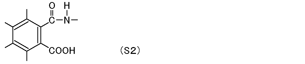
構造の異なるシランカップリング剤としては、例えば、上記式(S1)で示される構造単位を含むものと、上記式(S2)で示される構造単位を含むものとを含有することが好ましい。
本実施形態に係る感光性樹脂組成物は、溶解促進剤を含有してもよい。溶解促進剤は、感光性樹脂組成物を用いて形成された塗膜の露光部の現像液に対する溶解性を向上させ、パターニング時のスカムを改善することが可能な成分である。かかる溶解促進剤としては、フェノール性水酸基を有する化合物が好ましい。
ここで、ビフェノール型の骨格を備える溶解促進剤としては、例えば、下記一般式(D1)で表されるものが好ましい、また、ビスフェノールA型の骨格を備えるものとしては、例えば、下記一般式(D2)で表されるものが好ましい。

R3からR12は、それぞれ独立して、水素、ヒドロキシル基、または、炭素数1以上10以下の有機基であり、
R3からR7のうち少なくとも1つ、及び、R8からR12のうち少なくとも1つは、ヒドロキシル基を含む。)
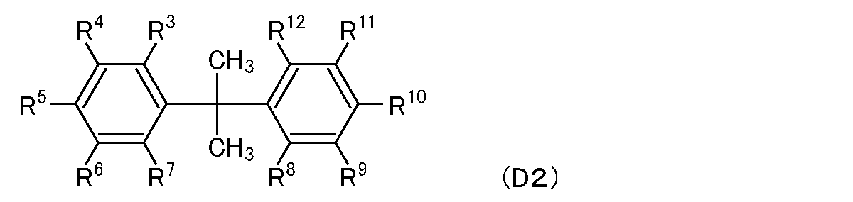
R3からR12は、それぞれ独立して、水素、ヒドロキシル基、または、炭素数1以上10以下の有機基であり、
R3からR7のうち少なくとも1つ、及び、R8からR12のうち少なくとも1つは、ヒドロキシル基を含む。)
なお、R3からR12は1価の有機基である。ここで、1価の有機基とは、原子価のことを示す。すなわち、R3からR12のそれぞれが他の原子と結合する結合手が1個であることを示す。
本実施形態に係る感光性樹脂組成物は、界面活性剤を含有してもよい。本実施形態に係る界面活性剤は、たとえば、フッ素基(たとえば、フッ素化アルキル基)、シラノール基を含む化合物、またはシロキサン結合を主骨格とする化合物を含むものである。
本実施形態においては上記界面活性剤として、フッ素系界面活性剤またはシリコーン系界面活性剤を用いることがより好ましく、フッ素系界面活性剤を用いることがとくに好ましい。かかるフッ素系界面活性剤の具体例としては、DIC社製のメガファックF-171、F-173、F-444、F-470、F-471、F-475、F-482、F-477、F-554、F-556およびF-557、住友スリーエム社製のノベックFC4430およびFC4432等が挙げられる。なお、フッ素系界面活性剤とは、フッ素基を備える界面活性剤を示す。
界面活性剤としては、例えば、フッ素系界面活性剤を含むことが好ましい。これにより、感光性樹脂組成物中の原料成分のなじみを向上できる。したがって、アルカリ可溶性樹脂の分散性を向上できる。また、フッ素系界面活性剤を含むことで、封止材10に対する、感光性樹脂組成物のなじみを向上できる。したがって、塗布性を向上できる。
感光性樹脂組成物は、溶剤を含有してもよい。この場合、感光性樹脂組成物は、たとえばワニス状となる。
かかる溶剤の具体例としては、N-メチル-2-ピロリドン、γ-ブチロラクトン(GBL)、N,N-ジメチルアセトアミド、ジメチルスルホキシド、ジエチレングリコールジメチルエーテル、ジエチレングリコールジエチルエーテル、ジエチレングリコールジブチルエーテル、プロピレングリコールモノメチルエーテル、ジプロピレングリコールモノメチルエーテル、プロピレングリコールモノメチルエーテルアセテート(PGMEA)、乳酸メチル、乳酸エチル、乳酸ブチル、メチル-1,3-ブチレングリコールアセテート、1,3-ブチレングリコール-3-モノメチルエーテル、ピルビン酸メチル、およびピルビン酸エチル及びメチル-3-メトキシプロピオネート等が挙げられる。これらは、1種を単独で使用してもよいし、2種以上を併用してもよい。
溶剤としては、上記具体例のうち、例えば、エステル結合を備えるものが好ましい。また、エステル結合を備える溶剤としては、例えば、複素環式化合物が好ましい。複素環式化合物としては、例えば、ラクトン環を含むものが好ましい。
本発明者らは、アルカリ可溶性樹脂と、溶剤との組み合わせについて検討した。その結果、アルカリ可溶性樹脂として、構造単位中に芳香族環を含むものは、溶剤に対する分散性が低かった。アルカリ可溶性樹脂の分散性が低い従来の感光性樹脂組成物において、感光性樹脂組成物からなる液滴の表面張力は、上述した特定の数値範囲内とならない。この場合、感光性樹脂組成物の塗布性が低く、半導体装置を作成できなかった。また、塗布を工夫し、半導体装置を作製したとしても、絶縁性樹脂膜と、封止材との密着性が低く、さらに、半導体装置の信頼性が低下してしまうという不都合があった。そこで、本発明者らが、その構造単位中に芳香族環を含むアルカリ可溶性樹脂を好適に分散できる溶剤について検討した結果、上述する特定の官能基、構造を備える溶剤は、アルカリ可溶性樹脂の分散性に優れることが判明した。
本実施形態に係る半導体封止用樹脂組成物としては、たとえば、熱硬化性樹脂と、無機充填材と、硬化剤とを含むエポキシ樹脂組成物が挙げられる。
熱硬化性樹脂の具体例としては、フェノールノボラック樹脂、クレゾールノボラック樹脂、ビスフェノールAノボラック樹脂、トリアジン骨格含有フェノールノボラック樹脂などのノボラック型フェノール樹脂;未変性のレゾールフェノール樹脂、桐油、アマニ油、クルミ油などで変性した油変性レゾールフェノール樹脂などのレゾール型フェノール樹脂などのフェノール樹脂;ビスフェノールA型エポキシ樹脂、ビスフェノールF型エポキシ樹脂、ビスフェノールS型エポキシ樹脂、ビスフェノールE型エポキシ樹脂、ビスフェノールM型エポキシ樹脂、ビスフェノールP型エポキシ樹脂、ビスフェノールZ型エポキシ樹脂などのビスフェノール型エポキシ樹脂;フェノールノボラック型エポキシ樹脂、クレゾールノボラック型エポキシ樹脂などのノボラック型エポキシ樹脂;ビフェニル型エポキシ樹脂、ビフェニルアラルキル型エポキシ樹脂、アリールアルキレン型エポキシ樹脂、ナフタレン型エポキシ樹脂、アントラセン型エポキシ樹脂、フェノキシ型エポキシ樹脂、ジシクロペンタジエン型エポキシ樹脂、ノルボルネン型エポキシ樹脂、アダマンタン型エポキシ樹脂、フルオレン型エポキシ樹脂などのエポキシ樹脂;ユリア(尿素)樹脂、メラミン樹脂などのトリアジン環を有する樹脂;不飽和ポリエステル樹脂;ビスマレイミド化合物などのマレイミド樹脂;ポリウレタン樹脂;ジアリルフタレート樹脂;シリコーン樹脂;ベンゾオキサジン樹脂;シアネートエステル樹脂;ポリイミド樹脂;ポリアミドイミド樹脂;ベンゾシクロブテン樹脂、ノボラック型シアネート樹脂、ビスフェノールA型シアネート樹脂、ビスフェノールE型シアネート樹脂、テトラメチルビスフェノールF型シアネート樹脂等のビスフェノール型シアネート樹脂などが挙げられる。これらの中の1種類を単独で用いてもよいし、異なる重量平均分子量を有する2種類以上を併用してもよく、1種類または2種類以上と、それらのプレポリマーを併用してもよい。
半導体封止用樹脂組成物がパラフィン系ワックスなどの離型剤を含む場合、従来の感光性樹脂組成物と、半導体封止用樹脂組成物との親和性が悪く、塗布性に劣るという不都合があった。しかしながら、本実施形態にかかる感光性樹脂組成物は、半導体封止用樹脂組成物との親和性が高いため、半導体封止用樹脂組成物が離型剤を含む場合でも好適な塗布性を発現できる観点で都合がよい。
また、半導体封止用樹脂組成物は、例えば、シランカップリング剤を含むことが好ましい。これにより、封止用樹脂組成物と、感光性樹脂組成物との親和性を向上でき、感光性樹脂組成物の塗布性を向上できる。なお、感光性樹脂組成物が、上記式(S1)または式(S2)で示される構造単位を含む場合、封止用樹脂組成物は、シランカップリング剤としてアミノシランを含むことが好ましい。これにより、封止用樹脂組成物と、感光性樹脂組成物との中に含まれるシランカップリング剤同士がアミド結合に由来する相互作用をし、さらに塗布性を向上できる。
本実施形態に係る粘着部材200は、半導体チップ40を接着できるものであれば、特に限定されないが、たとえば、支持フィルムと粘着剤層で構成されているものでもよい。
・アルカリ可溶性樹脂(A-1)の合成
温度計、攪拌機、原料投入口および乾燥窒素ガス導入管を備えた4つ口のガラス製セパラブルフラスコ内に、206.6g(0.8mol)のジフェニルエーテル-4,4'-ジカルボン酸と245.0g(1.6mol)の1-ヒドロキシ-1,2,3-ベンゾトリアゾール・一水和物とを反応させて得られたジカルボン酸誘導体の混合物422.8g(0.8mol)と、232.5g(0.9mol)の2,2-ビス(3-アミノ-4-ヒドロキシフェニル)プロパンと、23.2g(0.200mol)の3-アミノ-5-メルカプト-1、2、4-トリアゾールと、を入れた。その後、上記セパラブルフラスコ内に1583gのN-メチル-2-ピロリドンを加え、各原料成分を溶解させた。次に、オイルバスを用い、90℃で5時間反応させた。次いで、上記セパラブルフラスコ内に68.9g(0.4mol)の4-エチニルフタル酸無水物と、68.9gのN-メチル-2-ピロリドンとを加え、90℃で3時間攪拌しながら反応させた後、23℃まで冷却して反応を終了させた。

・アルカリ可溶性樹脂(A-2)の合成
温度計、攪拌機、原料投入口および乾燥窒素ガス導入管を備えた4つ口のガラス製セパラブルフラスコ内に、129.2g(0.5mol)の2,2-ビス(3-アミノ-4-ヒドロキシフェニル)プロパンを入れた。その後、上記セパラブルフラスコ内に1290mLのアセトンを加え、2,2-ビス(3-アミノ-4-ヒドロキシフェニル)プロパンを溶解させた。次に、予め185.6g(1.0mol)の4-ニトロベンゾイルクロリドをアセトン100mLに溶解させて得られた溶液を、温度が20℃未満となるように冷却しながら上記セパラブルフラスコ内に30分かけて滴下混合した。次いで、得られた混合液の温度を40℃に加熱してから2時間撹拌した後に、138.0g(1.0mol)の炭酸カリウムを徐々に添加してから、さらに2時間撹拌した。その後、混合液を加熱することなく、室温でさらに18時間撹拌した。次に、混合液を激しく撹拌しながら水酸化ナトリウム水溶液を徐々に添加した後、55℃に加温してさらに30分間撹拌した。撹拌終了後、混合液を室温まで冷却してから、かかる混合液のpHが6.0~7.0の範囲になるよう10重量%の塩酸水溶液を用いてpH調整を行った。次に、混合液中に析出した析出物を濾別して得られた濾液を水で洗浄した後、60~70℃の温度で乾燥させ、ビス-N,N'-(パラ-ニトロベンゾイル)-2,2-ビス(4-ヒドロキシフェニル)プロパンの固体を得た。



・アルカリ可溶性樹脂(A-3)の合成
温度計、攪拌機、原料投入口および乾燥窒素ガス導入管を備えた4つ口のガラス製セパラブルフラスコ内に、232.5g(0.9mol)の2,2-ビス(3-アミノ-4-ヒドロキシフェニル)プロパンと、23.2g(0.200mol)の3-アミノ-5-メルカプト-1、2、4-トリアゾールとを入れた。次に、かかるセパラブルフラスコ内に、597gのN-メチル-2-ピロリドンを添加し溶解させた。次に、118.0g(0.4mol)の4,4'-オキシジベンゾイルクロリドと、95.7g(0.4mol)のセバシン酸ジクロリドとをN-メチル-2-ピロリドン499gに予め溶解させて得た溶液を、温度が20℃未満になるよう冷却しながら上記セパラブルフラスコ内に30分かけて滴下した。滴下終了後、室温で24時間撹拌した。次に、68.9g(0.4mol)の4-エチニルフタル酸無水物と、68.9gのN-メチル-2-ピロリドンとを加え、さらに24時間攪拌混合してから反応を終了させた。

・アルカリ可溶性樹脂(A-4)の合成
温度計、攪拌機、原料投入口および乾燥窒素ガス導入管を備えた4つ口のガラス製丸底フラスコ内に、100.1g(0.50mol)の4,4-ジヒドロキシジフェニルメタンと、63.1g(0.50mol)のフロログルシノールと、169.6g(0.7mol)の4,4'-ビス(メトキシメチル)ビフェニルと、7.7g(0.05mol)のジエチル硫酸と、340gのγ-ブチロラクトンとを仕込んだ後、かかる丸底フラスコを油浴し、反応液を還流させながら100℃で6時間の重縮合反応を行った。次に、得られた反応液を室温まで冷却した後、800gのγ-ブチロラクトンを丸底フラスコ内に添加し均一になるまで撹拌混合した。その後、丸底フラスコ内にある反応液を水10Lに滴下混合することにより、樹脂成分を析出させた。次に、析出した樹脂成分を濾別して回収した後、50℃での真空乾燥を行うことにより、下記式(7)で表されるフェノール樹脂を、アルカリ可溶性樹脂(A-4)として得た。得られたアルカリ可溶性樹脂(A-4)の重量平均分子量は、9,800であった。

・感光剤(B-1)の合成
温度計、攪拌機、原料投入口、乾燥窒素ガス導入管を備えた4つ口のセパラブルフラスコ内に、11.04g(0.026mol)のTrisP-PA(本州化学社製)と、18.81g(0.070mol)の1,2-ナフトキノン-2-ジアジド-4-スルホニルクロライドと、170gのアセトンとを入れて、撹拌することにより溶解させた。
次いで、ウォーターバスを用いて、反応溶液の温度が35℃以上にならないようにフラスコを冷やしながら、かかるフラスコ内に、トリエチルアミン7.78g(0.077mol)およびアセトン5.5gの混合溶液をゆっくり滴下混合した。滴下後、室温で3時間反応させ、1.05g(0.017mol)の酢酸を添加しさらに30分反応させた。
次いで、セパラブルフラスコ内にある反応混合物を濾過して得られた濾液を、990mLの水と10mLの酢酸とからなる混合溶液に投入した。その後、沈殿物を濾別し、水で充分洗浄した後に、真空条件下、かかる沈殿物を乾燥させた。このようにして、下記式(8)で表されるジアゾナフトキノン化合物を、感光剤(B-1)として得た。
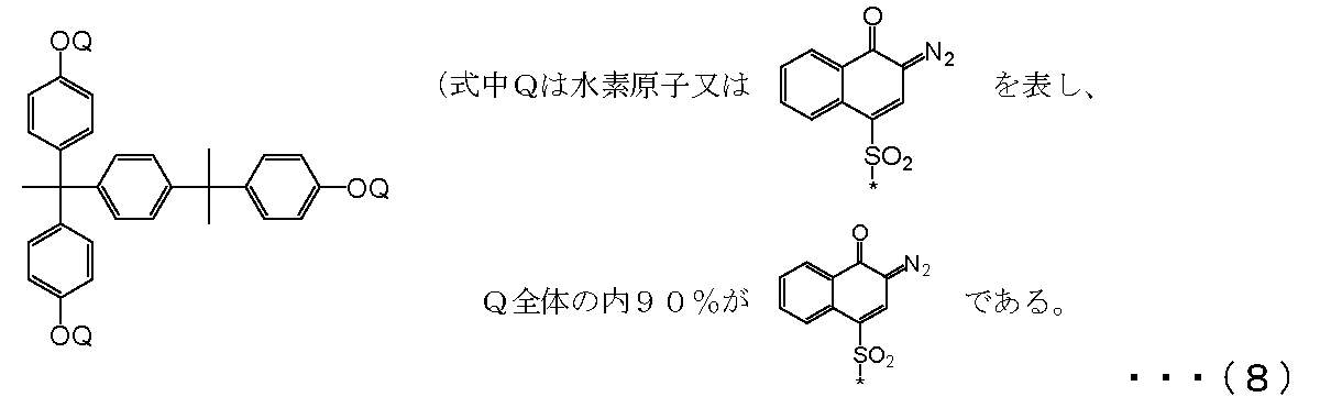
・シランカップリング剤(D-2)の合成
撹拌機および冷却管を備えた適切なサイズの反応容器内で、45.6g(300mmol)のシクロヘキセン-1,2-ジカルボン酸無水物を970gのγ-ブチルラクトンに溶解させ、恒温槽を用いて溶液の温度が30℃となるように温度調整を行った。次いで、62g(280mmol)の3-アミノプロピルトリエトキシシランを60分かけて、反応容器内に滴下混合した。滴下終了後、30℃で18時間撹拌混合することにより、下記式(9)で表されるシランカップリング剤(D-2)を得た。

・シランカップリング剤(D-3)の合成
撹拌機および冷却管を備えた適切なサイズの反応容器内で、32.2g(100mmol)の,3',4,4'-ベンゾフェノンテトラカルボン酸二無水物を669gのγ-ブチルラクトンに溶解させ、恒温槽を用いて溶液の温度が30℃となるように温度調整を行った。次いで、42.1g(190mmol)の3-アミノプロピルトリエトキシシランを60分かけて、反応容器内に滴下混合した。滴下終了後、30℃で18時間撹拌混合することにより、下記式(10)で表されるシランカップリング剤(D-3)を得た。
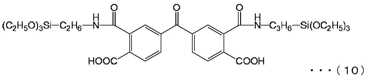
各実施例、各比較例の半導体装置の製造に用いた感光性樹脂組成物を作製した。以下、詳細を説明する。
まず、下記表1に示す配合量に従って溶剤(G)以外の各原料成分を、調合後の粘度が約500mPa・sとなるように、下記表1に示す量の溶剤(G)に溶解させてから、窒素雰囲気下で撹拌した。その後、孔径0.2μmのポリエチレン製フィルターで濾過して得られた濾液を、ワニス状の感光性樹脂組成物として得た。
感光性樹脂組成物の原料成分を下記に示す。
・アルカリ可溶性樹脂A-1:上記合成例1により得られたアルカリ可溶性樹脂(A-1)(ポリアミド樹脂)
・アルカリ可溶性樹脂A-2:上記合成例2により得られたアルカリ可溶性樹脂(A-2)(ポリアミド樹脂)
・アルカリ可溶性樹脂A-3:上記合成例3により得られたアルカリ可溶性樹脂(A-3)(ポリアミド樹脂)
・アルカリ可溶性樹脂A-4:上記合成例4により得られたアルカリ可溶性樹脂(A-4)(フェノール樹脂)
・アルカリ可溶性樹脂A-5:ポリヒドロキシスチレン樹脂(丸善石油社製、マルカリンカーS-1P)
・感光剤B-1:上記合成例5により得られた感光剤(B-1)(ジアゾナフトキノン化合物)
・熱架橋剤C-1:パラキシレングリコール(東京化成工業社製、下記式(11)中の(C-1))
・熱架橋剤C-2:テトラメトキシメチルグリコールウリル(三和ケミカル社製、ニカラック MX-270、下記式(11)中の(C-2))

・シランカップリング剤D-1:3-メタクリロキシプロピルトリメトキシシラン(信越シリコーン社製)
・シランカップリング剤D-2:上記合成例6により得られたシランカップリング剤
・シランカップリング剤D-3:上記合成例7により得られたシランカップリング剤
・溶解促進剤E-1:4,4'-ビフェノール(本州化学社製、下記式(12)中の(E-1))
・溶解促進剤E-2:2,2'-ビス(4-ヒドロキシ-3,5-ジメチルフェニル)プロパン(本州化学社製、Bis-26X-A、下記式(12)中の(E-2))

・界面活性剤F-1:フッ素系界面活性剤(DIC社製、メガファックF-556)
・界面活性剤F-2:フッ素系界面活性剤(住友スリーエム社製、FC4430)
・溶剤G-1:γ-ブチロラクトン(GBL)
・溶剤G-2:プロピレングリコールモノメチルエーテルアセテート(PGMEA)
・溶剤G-3:ホルムアミド
まず、ワニス状の感光性樹脂組成物を18Gのニードルがついたシリンジに充填し、全自動接触角計(協和界面化学社製、DM-901)を用いて、かかる感光性樹脂組成物からなる5μLの液滴を作成した。次いで、young-Laplace法により、作製した液滴の形状を解析して該液滴の表面張力を測定した。
評価結果を下記表1に示す。
評価結果を下記表1に示す。
各実施例に係る半導体装置は、以下の方法で作製した。
まず、表面にアルミ回路を備えており、かつ10mm×10mmの大きさにダイシングした模擬素子ウエハを、熱剥離性フィルムを貼ったSUS製のキャリアーにおける上記フィルムが貼り付けられている側の面上に、縦横それぞれ10mmの間隔を空けて配置した。このとき、模擬素子ウエハにおいてアルミ回路が、上記熱剥離性フィルムと対向する側の面を向くように、かかる模擬素子ウエハを配置する。次に、圧縮成形機を用いて、金型温度125℃、成形圧力5MPa、硬化時間10分の条件で、模擬素子ウエハを埋設するように、エポキシ樹脂組成物(住友ベークライト社製)の硬化物からなる封止材を成形した。なお、エポキシ樹脂組成物は、エポキシ樹脂として多官能エポキシ樹脂と、硬化剤として多官能フェノール樹脂と、無機充填材としてシリカと、カップリング剤としてアミノシランカップリング剤と、離型剤としてパラフィン系ワックスとを含むものであった。
次に、200℃に熱したホットプレートを用いて熱剥離性フィルムを、加熱しながらキャリアーから剥離し、その後、175℃、4時間の条件で後硬化(ポストキュア)することにより、図1(c)に示す半導体チップを内蔵した封止材樹脂基板(複数の半導体チップが封止材の内部に埋め込まれた構造体、以下、チップ内蔵封止材樹脂基板ともいう。)を得た。
まず、上述した方法で得られたチップ内蔵封止材樹脂基板における半導体チップが配されている側の面に対して、バッチ式プラズマ処理装置(March社製、AP-1000)を用い、出力エネルギー800W、ガス量200sccm、時間1分の条件で、酸素プラズマ処理を施した。次に、スピンコーターを用いて、チップ内蔵封止材樹脂基板における半導体チップが配されている側の面に対して、上述した方法で作製したワニス状の感光性樹脂組成物を塗布した後、ホットプレートで120℃、4分間のプリベーク処理を行うことにより、膜厚約9.0μmの樹脂膜を形成した。次いで、半導体チップのアルミ回路に対し、フォトマスクを介して、ブロードバンド露光機(マイクロテック社製、MA-8 SUSS)を用いて十分な露光処理を行った。その後、2.38重量%のテトラメチルアンモニウムヒドロキシド水溶液中において、樹脂膜の膜厚に関し、プリベーク後の膜厚と現像後の膜厚との差が1.5μmとなるように、現像時間を調節しながら2回のパドル現像処理を行うことで露光部を溶解除去してから、純水で10秒間リンスした。その後、酸素雰囲気下、230℃、90分の条件で熱処理して硬化させることにより、アルミ回路の一部を露出させるように開口部が設けられた絶縁性樹脂膜を作製した。以下、上記絶縁性樹脂膜を備えたチップ内蔵封止材樹脂基板のことを、樹脂膜付き封止材基板とも示す。
なお、実施例12は、実施例1と同じ感光性樹脂組成物を用いて、樹脂膜の硬化条件を酸素雰囲気下、温度180℃で30分間とすることで絶縁性樹脂膜を作製した。
また、実施例13は、実施例1と同じ感光性樹脂組成物を用いて、樹脂膜の硬化条件を酸素雰囲気下、温度250℃で30分間とすることで絶縁性樹脂膜を作製した。
上述した方法で得られた樹脂膜付き封止材基板における、開口部内に露出したアルミ回路と、絶縁性樹脂膜との上部に、スパッタ装置とレジストとを用いて、500ÅのTi膜と、3000ÅのCu膜とをこの順で取り付けてなるスパッタ膜を形成した。次に、上記スパッタ膜上に、Cuを用いて厚み7μmのめっき膜を形成した。その後、レジストを除去してから、上記スパッタ層を薬液でエッチングすることにより、Cuからなる配線層(Cu配線層)を有したCu配線層付き封止材基板を得た。
上述した方法で得られたCu配線層付き封止材基板におけるCu配線層が配されている側の面に対して、バッチ式プラズマ処理装置(March社製、AP-1000)を用い、出力エネルギー800W、ガス量200sccm、時間1分の条件で、酸素プラズマ処理を施した。次に、スピンコーターを用いて、Cu配線層付き封止材基板におけるCu配線層が配されている側の面に対して、上述した方法で作製したワニス状の感光性樹脂組成物を塗布した後、ホットプレートで120℃、4分間のプリベーク処理を行うことにより、膜厚約11.0μmの樹脂膜を形成した。次いで、Cu配線層付き封止材基板において半導体チップが配されている領域外に形成されているCu配線層の一部に、フォトマスクを介して、ブロードバンド露光機(マイクロテック社製、MA-8 SUSS)を用いて十分な露光処理を行った。その後、2.38重量%のテトラメチルアンモニウムヒドロキシド水溶液中において、樹脂膜の膜厚に関し、プリベーク後の膜厚と現像後の膜厚との差が1.5μmとなるように、現像時間を調節しながら2回のパドル現像処理を行うことで露光部を溶解除去してから、純水で10秒間リンスした。その後、酸素雰囲気下、230℃、90分の条件で熱処理して硬化させることにより、Cu配線層の一部を露出させるように開口部が設けられた絶縁性樹脂膜を作製し、所望の半導体装置を得た。
◎:半導体チップ内蔵封止材樹脂基板の表面全域に良好な形状の樹脂膜が形成されていた。
○:半導体チップ内蔵封止材樹脂基板の端から5mm以内の領域にハジキが発生していることが確認されたが、実用上問題ない程度のレベルであった。
×:半導体チップ内蔵封止材樹脂基板の端から5mmより大きく離れた領域に実用上問題があるレベルのハジキが発生していることが確認された。
次に、得られた上記樹脂膜に対して、カッターを用いて、縦横に1mm間隔で11個ずつ切れこみを入れた。このようにして、100個の独立した樹脂膜を有する構造体を得た。次に、得られた構造体に対して、プレッシャークッカーテスター装置を用いて、125℃、相対湿度100%、300時間の処理(プレッシャークッカー処理)を行なった。次に、上記処理後の構造体における樹脂膜に対して、接着力が3N/10mm以上のセロテープ(商標登録)を十分に貼り付けてから該テープを剥離するという剥離試験を実施した。以下の表1は、上記剥離試験により剥離した樹脂膜の数を示す。
なお、比較例1に係るワニス状の感光性樹脂組成物は、半導体チップ内蔵封止材樹脂基板に対して、ハジキが生じるため、膜厚が10μmとなるように塗布できなかった。したがって、密着性の評価は行わなかった。
評価結果は下記の通りとした。
◎:10個すべての半導体装置において剥離及びクラックが観察されなかった。
○:10個中1個の半導体装置において剥離またはクラックが観察された。
△:10個中2個の半導体装置において剥離またはクラックが観察されたが、歩留り上問題の無いものであった。
×:10個中3個以上の半導体装置において剥離またはクラックが観察された。
なお、比較例1に係るワニス状の感光性樹脂組成物は、半導体チップ内蔵封止材樹脂基板に対して、ハジキが生じるため、膜厚約9.0μmとなるように塗布できなかった。したがって、半導体装置を作成できなかったため、信頼性の評価は行わなかった。

また、比較例1の感光性樹脂組成物を用いた場合、ハジキが発生してしまうことに起因し、封止材上に所望の絶縁性樹脂膜を形成することはできなかった。すなわち、比較例1の感光性樹脂組成物を用いた場合、所望の半導体装置を作製することはできなかった。
また、比較例2の半導体装置として、上述した実施例1と同じ感光性樹脂組成物を用いて、酸素プラズマ処理を行わずに、実施例1と同様の方法で半導体装置を作製した。
具体的には、第1の絶縁性樹脂膜を形成する際、チップ内蔵封止材樹脂基板における半導体チップが配されている側の面に対して、酸素プラズマ処理を行わなかった。また、第2の絶縁性樹脂膜を形成する際に、Cu配線層付き封止材基板におけるCu配線層が配されている側の面に対して、酸素プラズマ処理を行わなかった。これら以外については、実施例1と同様の方法で半導体装置を作成し、比較例2の半導体装置を得た。

Claims (16)
- 表面に接続端子を有した複数の半導体チップが、封止材の内部に埋め込まれた構造体を準備する工程と、
前記構造体における前記半導体チップに設けられた接続端子が配されている側の面上領域に第1の絶縁性樹脂膜を形成する工程と、
前記第1の絶縁性樹脂膜および前記構造体に、前記接続端子の一部を露出させる第1の開口部を形成する工程と、
露出した前記接続端子と、前記第1の絶縁性樹脂膜の少なくとも一部とを覆うように導電膜を形成する工程と、
前記導電膜の表面に第2の絶縁性樹脂膜を形成する工程と、
前記第2の絶縁性樹脂膜における前記半導体チップ上に形成された領域の外部に、前記導電膜の一部を露出させる第2の開口部を形成する工程と、
を含み、
前記第1の絶縁性樹脂膜を構成する樹脂材料が、アルカリ可溶性樹脂を含む感光性樹脂組成物であって、
懸滴法により測定した前記感光性樹脂組成物からなる液滴の表面張力が、20mN/m以上45mN/m以下である、半導体装置の製造方法。 - 前記アルカリ可溶性樹脂が、フェノール樹脂、ヒドロキシスチレン樹脂、ポリイミド、ポリイミド前駆体、ポリベンゾオキサゾール、ポリベンゾオキサゾール前駆体、環状オレフィン系樹脂、およびこれらの共重合体からなる群より選択される1種または2種以上を含む、請求項1に記載の半導体装置の製造方法。
- 前記アルカリ可溶性樹脂が、前記ポリイミド前駆体、または、前記ポリベンゾオキサゾール前駆体を含み、
前記ポリイミド前駆体及び前記ポリベンゾオキサゾール前駆体は、その構造単位中に芳香族環を含む、請求項2に記載の半導体装置の製造方法。 - 前記感光性樹脂組成物を、230℃、90分の条件で熱処理することにより得られた10mm×60mm×10μm厚の硬化物を試験片として用い、23℃、延伸速度5mm/分の条件でJIS K7161に準拠した方法により引張試験を行った際における、前記試験片の引張伸び率が20%以上200%以下である、請求項1乃至3のいずれか1項に記載の半導体装置の製造方法。
- 前記感光性樹脂組成物を、230℃、90分の条件で熱処理することにより得られた硬化物のガラス転移温度が180℃以上である、請求項1乃至4のいずれか一項に記載の半導体装置の製造方法。
- 前記第2の絶縁樹脂膜を構成する樹脂材料が、前記感光性樹脂組成物である、請求項1乃至5のいずれか一項に記載の半導体装置の製造方法。
- 前記第1の絶縁性樹脂膜を形成する工程の前に、前記封止材の表面に対してプラズマ処理を施す工程をさらに含む、請求項1乃至6のいずれか一項に記載の半導体装置の製造方法。
- 前記封止材が、エポキシ樹脂と、無機充填材と、硬化剤とを含むエポキシ樹脂組成物の硬化物である、請求項1乃至7のいずれか一項に記載の半導体装置の製造方法。
- 前記感光性樹脂組成物は、感光剤をさらに含み、
前記感光剤は、光活性化合物である、請求項1乃至8のいずれか一項に記載の半導体装置の製造方法。 - 前記感光性樹脂組成物は、架橋剤をさらに含み、
前記架橋剤は、エポキシ化合物、アルコキシメチル化合物、メチロール化合物、及び、オキセタン化合物から選択される1種又は2種以上である、請求項1乃至9のいずれか一項に記載の半導体装置の製造方法。 - 前記架橋剤は、構造の異なる2種以上を含む、請求項10に記載の半導体装置の製造方法。
- 前記感光性樹脂組成物は、シランカップリング剤をさらに含み、
前記シランカップリング剤は、下記式(S1)または下記式(S2)で示される構造単位を含む、請求項1乃至11のいずれか一項に記載の半導体装置の製造方法。
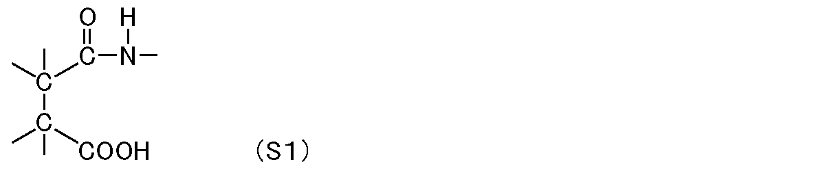
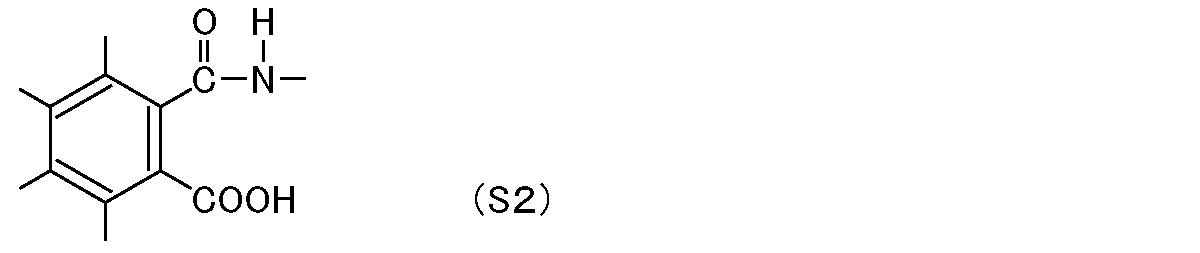
- 前記シランカップリング剤は、構造の異なる2種以上を含む、請求項12に記載の半導体装置の製造方法。
- 前記感光性樹脂組成物は、溶解促進剤を更に含み、
前記溶解促進剤は、下記一般式(D1)または下記一般式(D2)で表されるものを含む、請求項1から13のいずれか一項に記載の半導体装置の製造方法。
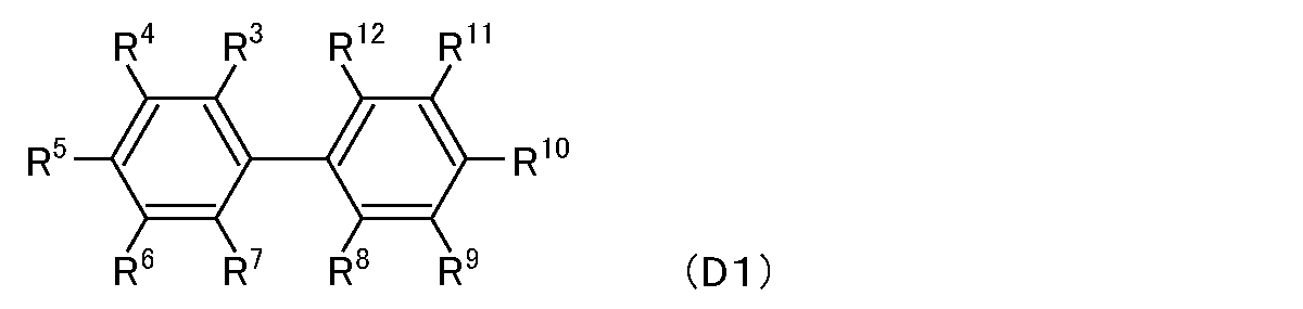
R3からR12は、それぞれ独立して、水素、ヒドロキシル基、または、炭素数1以上10以下の有機基であり、
R3からR7のうち少なくとも1つ、及び、R8からR12のうち少なくとも1つは、ヒドロキシル基を含む。)

R3からR12は、それぞれ独立して、水素、ヒドロキシル基、または、炭素数1以上10以下の有機基であり、
R3からR7のうち少なくとも1つ、及び、R8からR12のうち少なくとも1つは、ヒドロキシル基を含む。) - 前記感光性樹脂組成物は、界面活性剤を更に含み、
前記界面活性剤は、フッ素系界面活性剤を含む、請求項1乃至14のいずれか一項に記載の半導体装置の製造方法。 - 前記感光性樹脂組成物は、溶剤を更に含み、
前記溶剤は、エステル結合を備える、請求項1乃至15のいずれか一項に記載の半導体装置の製造方法。
Priority Applications (3)
| Application Number | Priority Date | Filing Date | Title |
|---|---|---|---|
| CN201780054916.7A CN109690759B (zh) | 2016-09-08 | 2017-09-04 | 半导体装置的制造方法 |
| KR1020197009608A KR102028870B1 (ko) | 2016-09-08 | 2017-09-04 | 반도체 장치의 제조 방법 |
| JP2017563145A JP6477925B2 (ja) | 2016-09-08 | 2017-09-04 | 半導体装置の製造方法 |
Applications Claiming Priority (2)
| Application Number | Priority Date | Filing Date | Title |
|---|---|---|---|
| JP2016-175593 | 2016-09-08 | ||
| JP2016175593 | 2016-09-08 |
Publications (1)
| Publication Number | Publication Date |
|---|---|
| WO2018047770A1 true WO2018047770A1 (ja) | 2018-03-15 |
Family
ID=61562071
Family Applications (1)
| Application Number | Title | Priority Date | Filing Date |
|---|---|---|---|
| PCT/JP2017/031795 Ceased WO2018047770A1 (ja) | 2016-09-08 | 2017-09-04 | 半導体装置の製造方法 |
Country Status (5)
| Country | Link |
|---|---|
| JP (1) | JP6477925B2 (ja) |
| KR (1) | KR102028870B1 (ja) |
| CN (1) | CN109690759B (ja) |
| TW (1) | TWI745426B (ja) |
| WO (1) | WO2018047770A1 (ja) |
Cited By (8)
| Publication number | Priority date | Publication date | Assignee | Title |
|---|---|---|---|---|
| JP2021028926A (ja) * | 2019-08-09 | 2021-02-25 | 住友ベークライト株式会社 | 電子装置の製造方法 |
| JP2021128300A (ja) * | 2020-02-17 | 2021-09-02 | 住友ベークライト株式会社 | 感光性樹脂組成物、および半導体装置の製造方法 |
| JPWO2021241447A1 (ja) * | 2020-05-26 | 2021-12-02 | ||
| JP2023520280A (ja) * | 2020-04-03 | 2023-05-17 | 京東方科技集團股▲ふん▼有限公司 | 無機発光ダイオード基板及びその製造方法 |
| CN117059583A (zh) * | 2023-10-12 | 2023-11-14 | 江苏芯德半导体科技有限公司 | 一种具有异质胶材的晶圆级扇出型封装结构及其封装方法 |
| JP2025506765A (ja) * | 2022-12-07 | 2025-03-13 | タコマ テクノロジー カンパニー リミテッド | 感光性樹脂及びそれを含むフォトレジスト組成物 |
| WO2025069827A1 (ja) * | 2023-09-29 | 2025-04-03 | 太陽ホールディングス株式会社 | ネガ型感光性樹脂組成物、ドライフィルム、硬化物および電子部品 |
| WO2026063317A1 (ja) * | 2024-09-17 | 2026-03-26 | 太陽ホールディングス株式会社 | 硬化性樹脂組成物、ドライフィルム、及び、硬化物 |
Families Citing this family (5)
| Publication number | Priority date | Publication date | Assignee | Title |
|---|---|---|---|---|
| US11024593B2 (en) | 2018-09-28 | 2021-06-01 | Taiwan Semiconductor Manufacturing Co., Ltd. | Metal bumps and method forming same |
| US12079551B2 (en) * | 2019-06-11 | 2024-09-03 | Canon Kabushiki Kaisha | Simulation method, simulation apparatus, storage medium, film forming method, and method of producing cured product |
| WO2021241581A1 (ja) * | 2020-05-29 | 2021-12-02 | 住友ベークライト株式会社 | 感光性樹脂組成物 |
| KR102587322B1 (ko) * | 2021-05-28 | 2023-10-10 | 삼성에스디아이 주식회사 | 반도체 소자 밀봉용 에폭시 수지 조성물 및 이를 사용하여 밀봉된 반도체 소자 |
| CN113817426B (zh) * | 2021-08-25 | 2023-06-30 | 上海锐朗光电材料有限公司 | 一种应用于大尺寸芯片粘接的导电胶及其制备方法 |
Citations (7)
| Publication number | Priority date | Publication date | Assignee | Title |
|---|---|---|---|---|
| JP2008506010A (ja) * | 2004-07-07 | 2008-02-28 | プロメラス, エルエルシー | 絶縁樹脂組成物及びその使用 |
| JP2009283931A (ja) * | 2008-04-25 | 2009-12-03 | Hitachi Chem Co Ltd | 絶縁層、絶縁体インク及び両面電極パッケージ |
| WO2014069091A1 (ja) * | 2012-10-30 | 2014-05-08 | 住友ベークライト株式会社 | 感光性樹脂組成物、硬化膜、保護膜、絶縁膜および電子装置 |
| JP2015053469A (ja) * | 2013-08-07 | 2015-03-19 | 日東電工株式会社 | 半導体パッケージの製造方法 |
| JP2015064576A (ja) * | 2013-08-29 | 2015-04-09 | 住友ベークライト株式会社 | 感光性樹脂組成物 |
| JP2015173253A (ja) * | 2014-02-20 | 2015-10-01 | 株式会社テラプローブ | 半導体装置の製造方法 |
| JP2016023226A (ja) * | 2014-07-18 | 2016-02-08 | 旭化成イーマテリアルズ株式会社 | パワー半導体素子用保護膜、及びその形成方法 |
Family Cites Families (10)
| Publication number | Priority date | Publication date | Assignee | Title |
|---|---|---|---|---|
| JP2925960B2 (ja) * | 1994-11-29 | 1999-07-28 | 三洋電機株式会社 | 半導体装置の製造方法 |
| JP3818124B2 (ja) | 2001-10-25 | 2006-09-06 | 凸版印刷株式会社 | 半導体集積回路装置およびその製造方法 |
| US7382059B2 (en) | 2005-11-18 | 2008-06-03 | Semiconductor Components Industries, L.L.C. | Semiconductor package structure and method of manufacture |
| CN101833241B (zh) * | 2009-03-09 | 2012-07-04 | 村上精密制版(昆山)有限公司 | 一种感光性树脂组合物 |
| JP5678492B2 (ja) * | 2010-06-30 | 2015-03-04 | 日産化学工業株式会社 | パターン画像の形成方法 |
| TWI430024B (zh) * | 2010-08-05 | 2014-03-11 | 旭化成電子材料股份有限公司 | A photosensitive resin composition, a method for manufacturing a hardened bump pattern, and a semiconductor device |
| JP5820825B2 (ja) * | 2011-01-18 | 2015-11-24 | 旭化成イーマテリアルズ株式会社 | 樹脂組成物、硬化物、樹脂フィルム及び配線板 |
| JP6171583B2 (ja) | 2013-05-31 | 2017-08-02 | 富士通株式会社 | 電子装置及びその製造方法 |
| JP5672403B1 (ja) | 2014-05-26 | 2015-02-18 | 住友ベークライト株式会社 | 感光性樹脂組成物および電子装置 |
| TWI627502B (zh) * | 2014-09-04 | 2018-06-21 | Fujifilm Corp | 感光性樹脂組成物、硬化膜的製造方法、硬化膜、液晶顯示裝置、有機電激發光顯示裝置及觸控面板 |
-
2017
- 2017-09-04 KR KR1020197009608A patent/KR102028870B1/ko active Active
- 2017-09-04 JP JP2017563145A patent/JP6477925B2/ja active Active
- 2017-09-04 CN CN201780054916.7A patent/CN109690759B/zh active Active
- 2017-09-04 WO PCT/JP2017/031795 patent/WO2018047770A1/ja not_active Ceased
- 2017-09-07 TW TW106130554A patent/TWI745426B/zh active
Patent Citations (7)
| Publication number | Priority date | Publication date | Assignee | Title |
|---|---|---|---|---|
| JP2008506010A (ja) * | 2004-07-07 | 2008-02-28 | プロメラス, エルエルシー | 絶縁樹脂組成物及びその使用 |
| JP2009283931A (ja) * | 2008-04-25 | 2009-12-03 | Hitachi Chem Co Ltd | 絶縁層、絶縁体インク及び両面電極パッケージ |
| WO2014069091A1 (ja) * | 2012-10-30 | 2014-05-08 | 住友ベークライト株式会社 | 感光性樹脂組成物、硬化膜、保護膜、絶縁膜および電子装置 |
| JP2015053469A (ja) * | 2013-08-07 | 2015-03-19 | 日東電工株式会社 | 半導体パッケージの製造方法 |
| JP2015064576A (ja) * | 2013-08-29 | 2015-04-09 | 住友ベークライト株式会社 | 感光性樹脂組成物 |
| JP2015173253A (ja) * | 2014-02-20 | 2015-10-01 | 株式会社テラプローブ | 半導体装置の製造方法 |
| JP2016023226A (ja) * | 2014-07-18 | 2016-02-08 | 旭化成イーマテリアルズ株式会社 | パワー半導体素子用保護膜、及びその形成方法 |
Cited By (16)
| Publication number | Priority date | Publication date | Assignee | Title |
|---|---|---|---|---|
| JP2021028926A (ja) * | 2019-08-09 | 2021-02-25 | 住友ベークライト株式会社 | 電子装置の製造方法 |
| JP7322580B2 (ja) | 2019-08-09 | 2023-08-08 | 住友ベークライト株式会社 | 電子装置の製造方法 |
| JP2021128300A (ja) * | 2020-02-17 | 2021-09-02 | 住友ベークライト株式会社 | 感光性樹脂組成物、および半導体装置の製造方法 |
| JP2023520280A (ja) * | 2020-04-03 | 2023-05-17 | 京東方科技集團股▲ふん▼有限公司 | 無機発光ダイオード基板及びその製造方法 |
| US12206049B2 (en) | 2020-04-03 | 2025-01-21 | Boe Technology Group Co., Ltd. | Inorganic light-emitting diode substrate and manufacturing method thereof, and inorganic light-emitting diode display device |
| JP7709435B2 (ja) | 2020-05-26 | 2025-07-16 | ローム株式会社 | 半導体装置 |
| CN115699295A (zh) * | 2020-05-26 | 2023-02-03 | 罗姆股份有限公司 | 半导体装置以及半导体装置的制造方法 |
| WO2021241447A1 (ja) * | 2020-05-26 | 2021-12-02 | ローム株式会社 | 半導体装置、および半導体装置の製造方法 |
| JPWO2021241447A1 (ja) * | 2020-05-26 | 2021-12-02 | ||
| US12431399B2 (en) | 2020-05-26 | 2025-09-30 | Rohm Co., Ltd. | Semiconductor device and method for manufacturing semiconductor device |
| JP2025506765A (ja) * | 2022-12-07 | 2025-03-13 | タコマ テクノロジー カンパニー リミテッド | 感光性樹脂及びそれを含むフォトレジスト組成物 |
| JP7807119B2 (ja) | 2022-12-07 | 2026-01-27 | タコマ テクノロジー カンパニー リミテッド | 感光性樹脂及びそれを含むフォトレジスト組成物 |
| WO2025069827A1 (ja) * | 2023-09-29 | 2025-04-03 | 太陽ホールディングス株式会社 | ネガ型感光性樹脂組成物、ドライフィルム、硬化物および電子部品 |
| CN117059583A (zh) * | 2023-10-12 | 2023-11-14 | 江苏芯德半导体科技有限公司 | 一种具有异质胶材的晶圆级扇出型封装结构及其封装方法 |
| CN117059583B (zh) * | 2023-10-12 | 2024-01-09 | 江苏芯德半导体科技有限公司 | 一种具有异质胶材的晶圆级扇出型封装结构及其封装方法 |
| WO2026063317A1 (ja) * | 2024-09-17 | 2026-03-26 | 太陽ホールディングス株式会社 | 硬化性樹脂組成物、ドライフィルム、及び、硬化物 |
Also Published As
| Publication number | Publication date |
|---|---|
| JPWO2018047770A1 (ja) | 2018-09-06 |
| CN109690759B (zh) | 2020-05-22 |
| TW201826023A (zh) | 2018-07-16 |
| KR20190039613A (ko) | 2019-04-12 |
| KR102028870B1 (ko) | 2019-10-04 |
| CN109690759A (zh) | 2019-04-26 |
| TWI745426B (zh) | 2021-11-11 |
| JP6477925B2 (ja) | 2019-03-06 |
Similar Documents
| Publication | Publication Date | Title |
|---|---|---|
| JP6477925B2 (ja) | 半導体装置の製造方法 | |
| CN100477179C (zh) | 半导体装置、缓冲层用树脂组合物、芯片键合用树脂组合物以及封装用树脂组合物 | |
| JP7238271B2 (ja) | 電子装置、及び電子装置の製造方法 | |
| JP5672403B1 (ja) | 感光性樹脂組成物および電子装置 | |
| JPWO2017170032A1 (ja) | 感光性フィルム | |
| CN102822961B (zh) | 电路基板、半导体装置、电路基板的制造方法以及半导体装置的制造方法 | |
| TWI442184B (zh) | 正型感光性樹脂組成物、光阻圖案的製造方法及電子零件 | |
| JP2018093120A (ja) | 樹脂シート | |
| CN101679721A (zh) | 树脂组合物、填埋材料、绝缘层以及半导体装置 | |
| KR101846114B1 (ko) | 감광성 수지 조성물, 경화막, 보호막, 절연막 및 전자 장치 | |
| JP2016213321A (ja) | 半導体装置の製造方法及び半導体装置 | |
| TW202307979A (zh) | 半導體晶片接著用樹脂薄片 | |
| TWI832816B (zh) | 感光性樹脂組成物、樹脂膜及電子裝置 | |
| JP7062943B2 (ja) | 感光性接着剤組成物および構造体 | |
| TW202348699A (zh) | 表面改質材料用樹脂組成物 | |
| JP2023126287A (ja) | ソルダーレジスト樹脂組成物、樹脂シート、梱包体及び回路基板 | |
| JP2020019864A (ja) | 感光性接着材組成物、および構造体 | |
| TW201803937A (zh) | 樹脂片 | |
| JP5741745B1 (ja) | 感光性樹脂組成物、および樹脂膜 | |
| JP2013105834A (ja) | 半導体装置の製造方法、半導体装置及び電子部品 | |
| KR20240042666A (ko) | 감광성 수지 조성물, 전자 디바이스의 제조 방법 및 전자 디바이스 | |
| JP2015184674A (ja) | 感光性樹脂組成物、および樹脂膜 | |
| JP7322580B2 (ja) | 電子装置の製造方法 | |
| JP2019151717A (ja) | 封止用樹脂組成物 | |
| CN120604330A (zh) | 层叠体、半导体元件及mems元件 |
Legal Events
| Date | Code | Title | Description |
|---|---|---|---|
| WWE | Wipo information: entry into national phase |
Ref document number: 2017563145 Country of ref document: JP |
|
| 121 | Ep: the epo has been informed by wipo that ep was designated in this application |
Ref document number: 17848710 Country of ref document: EP Kind code of ref document: A1 |
|
| NENP | Non-entry into the national phase |
Ref country code: DE |
|
| ENP | Entry into the national phase |
Ref document number: 20197009608 Country of ref document: KR Kind code of ref document: A |
|
| 122 | Ep: pct application non-entry in european phase |
Ref document number: 17848710 Country of ref document: EP Kind code of ref document: A1 |