US11024593B2 - Metal bumps and method forming same - Google Patents
Metal bumps and method forming same Download PDFInfo
- Publication number
- US11024593B2 US11024593B2 US16/458,719 US201916458719A US11024593B2 US 11024593 B2 US11024593 B2 US 11024593B2 US 201916458719 A US201916458719 A US 201916458719A US 11024593 B2 US11024593 B2 US 11024593B2
- Authority
- US
- United States
- Prior art keywords
- polymer layer
- opening
- layer
- metal pad
- degrees
- Prior art date
- Legal status (The legal status is an assumption and is not a legal conclusion. Google has not performed a legal analysis and makes no representation as to the accuracy of the status listed.)
- Active
Links
Images


Classifications
-
- H—ELECTRICITY
- H01—ELECTRIC ELEMENTS
- H01L—SEMICONDUCTOR DEVICES NOT COVERED BY CLASS H10
- H01L24/00—Arrangements for connecting or disconnecting semiconductor or solid-state bodies; Methods or apparatus related thereto
- H01L24/01—Means for bonding being attached to, or being formed on, the surface to be connected, e.g. chip-to-package, die-attach, "first-level" interconnects; Manufacturing methods related thereto
- H01L24/10—Bump connectors ; Manufacturing methods related thereto
- H01L24/11—Manufacturing methods
-
- H—ELECTRICITY
- H01—ELECTRIC ELEMENTS
- H01L—SEMICONDUCTOR DEVICES NOT COVERED BY CLASS H10
- H01L21/00—Processes or apparatus adapted for the manufacture or treatment of semiconductor or solid state devices or of parts thereof
- H01L21/02—Manufacture or treatment of semiconductor devices or of parts thereof
- H01L21/04—Manufacture or treatment of semiconductor devices or of parts thereof the devices having at least one potential-jump barrier or surface barrier, e.g. PN junction, depletion layer or carrier concentration layer
- H01L21/18—Manufacture or treatment of semiconductor devices or of parts thereof the devices having at least one potential-jump barrier or surface barrier, e.g. PN junction, depletion layer or carrier concentration layer the devices having semiconductor bodies comprising elements of Group IV of the Periodic System or AIIIBV compounds with or without impurities, e.g. doping materials
- H01L21/30—Treatment of semiconductor bodies using processes or apparatus not provided for in groups H01L21/20 - H01L21/26
- H01L21/324—Thermal treatment for modifying the properties of semiconductor bodies, e.g. annealing, sintering
-
- H—ELECTRICITY
- H01—ELECTRIC ELEMENTS
- H01L—SEMICONDUCTOR DEVICES NOT COVERED BY CLASS H10
- H01L21/00—Processes or apparatus adapted for the manufacture or treatment of semiconductor or solid state devices or of parts thereof
- H01L21/02—Manufacture or treatment of semiconductor devices or of parts thereof
- H01L21/04—Manufacture or treatment of semiconductor devices or of parts thereof the devices having at least one potential-jump barrier or surface barrier, e.g. PN junction, depletion layer or carrier concentration layer
- H01L21/48—Manufacture or treatment of parts, e.g. containers, prior to assembly of the devices, using processes not provided for in a single one of the subgroups H01L21/06 - H01L21/326
- H01L21/4814—Conductive parts
-
- H—ELECTRICITY
- H01—ELECTRIC ELEMENTS
- H01L—SEMICONDUCTOR DEVICES NOT COVERED BY CLASS H10
- H01L23/00—Details of semiconductor or other solid state devices
- H01L23/28—Encapsulations, e.g. encapsulating layers, coatings, e.g. for protection
- H01L23/31—Encapsulations, e.g. encapsulating layers, coatings, e.g. for protection characterised by the arrangement or shape
- H01L23/3157—Partial encapsulation or coating
- H01L23/3192—Multilayer coating
-
- H—ELECTRICITY
- H01—ELECTRIC ELEMENTS
- H01L—SEMICONDUCTOR DEVICES NOT COVERED BY CLASS H10
- H01L23/00—Details of semiconductor or other solid state devices
- H01L23/48—Arrangements for conducting electric current to or from the solid state body in operation, e.g. leads, terminal arrangements ; Selection of materials therefor
- H01L23/481—Internal lead connections, e.g. via connections, feedthrough structures
-
- H—ELECTRICITY
- H01—ELECTRIC ELEMENTS
- H01L—SEMICONDUCTOR DEVICES NOT COVERED BY CLASS H10
- H01L23/00—Details of semiconductor or other solid state devices
- H01L23/48—Arrangements for conducting electric current to or from the solid state body in operation, e.g. leads, terminal arrangements ; Selection of materials therefor
- H01L23/482—Arrangements for conducting electric current to or from the solid state body in operation, e.g. leads, terminal arrangements ; Selection of materials therefor consisting of lead-in layers inseparably applied to the semiconductor body
- H01L23/485—Arrangements for conducting electric current to or from the solid state body in operation, e.g. leads, terminal arrangements ; Selection of materials therefor consisting of lead-in layers inseparably applied to the semiconductor body consisting of layered constructions comprising conductive layers and insulating layers, e.g. planar contacts
-
- H—ELECTRICITY
- H01—ELECTRIC ELEMENTS
- H01L—SEMICONDUCTOR DEVICES NOT COVERED BY CLASS H10
- H01L23/00—Details of semiconductor or other solid state devices
- H01L23/48—Arrangements for conducting electric current to or from the solid state body in operation, e.g. leads, terminal arrangements ; Selection of materials therefor
- H01L23/488—Arrangements for conducting electric current to or from the solid state body in operation, e.g. leads, terminal arrangements ; Selection of materials therefor consisting of soldered or bonded constructions
- H01L23/495—Lead-frames or other flat leads
- H01L23/49517—Additional leads
- H01L23/4952—Additional leads the additional leads being a bump or a wire
-
- H—ELECTRICITY
- H01—ELECTRIC ELEMENTS
- H01L—SEMICONDUCTOR DEVICES NOT COVERED BY CLASS H10
- H01L23/00—Details of semiconductor or other solid state devices
- H01L23/48—Arrangements for conducting electric current to or from the solid state body in operation, e.g. leads, terminal arrangements ; Selection of materials therefor
- H01L23/488—Arrangements for conducting electric current to or from the solid state body in operation, e.g. leads, terminal arrangements ; Selection of materials therefor consisting of soldered or bonded constructions
- H01L23/498—Leads, i.e. metallisations or lead-frames on insulating substrates, e.g. chip carriers
- H01L23/49811—Additional leads joined to the metallisation on the insulating substrate, e.g. pins, bumps, wires, flat leads
-
- H—ELECTRICITY
- H01—ELECTRIC ELEMENTS
- H01L—SEMICONDUCTOR DEVICES NOT COVERED BY CLASS H10
- H01L23/00—Details of semiconductor or other solid state devices
- H01L23/52—Arrangements for conducting electric current within the device in operation from one component to another, i.e. interconnections, e.g. wires, lead frames
- H01L23/522—Arrangements for conducting electric current within the device in operation from one component to another, i.e. interconnections, e.g. wires, lead frames including external interconnections consisting of a multilayer structure of conductive and insulating layers inseparably formed on the semiconductor body
- H01L23/5226—Via connections in a multilevel interconnection structure
-
- H—ELECTRICITY
- H01—ELECTRIC ELEMENTS
- H01L—SEMICONDUCTOR DEVICES NOT COVERED BY CLASS H10
- H01L24/00—Arrangements for connecting or disconnecting semiconductor or solid-state bodies; Methods or apparatus related thereto
- H01L24/01—Means for bonding being attached to, or being formed on, the surface to be connected, e.g. chip-to-package, die-attach, "first-level" interconnects; Manufacturing methods related thereto
- H01L24/02—Bonding areas ; Manufacturing methods related thereto
- H01L24/07—Structure, shape, material or disposition of the bonding areas after the connecting process
- H01L24/08—Structure, shape, material or disposition of the bonding areas after the connecting process of an individual bonding area
-
- H—ELECTRICITY
- H01—ELECTRIC ELEMENTS
- H01L—SEMICONDUCTOR DEVICES NOT COVERED BY CLASS H10
- H01L24/00—Arrangements for connecting or disconnecting semiconductor or solid-state bodies; Methods or apparatus related thereto
- H01L24/01—Means for bonding being attached to, or being formed on, the surface to be connected, e.g. chip-to-package, die-attach, "first-level" interconnects; Manufacturing methods related thereto
- H01L24/10—Bump connectors ; Manufacturing methods related thereto
- H01L24/12—Structure, shape, material or disposition of the bump connectors prior to the connecting process
- H01L24/13—Structure, shape, material or disposition of the bump connectors prior to the connecting process of an individual bump connector
-
- H—ELECTRICITY
- H01—ELECTRIC ELEMENTS
- H01L—SEMICONDUCTOR DEVICES NOT COVERED BY CLASS H10
- H01L24/00—Arrangements for connecting or disconnecting semiconductor or solid-state bodies; Methods or apparatus related thereto
- H01L24/01—Means for bonding being attached to, or being formed on, the surface to be connected, e.g. chip-to-package, die-attach, "first-level" interconnects; Manufacturing methods related thereto
- H01L24/10—Bump connectors ; Manufacturing methods related thereto
- H01L24/15—Structure, shape, material or disposition of the bump connectors after the connecting process
- H01L24/16—Structure, shape, material or disposition of the bump connectors after the connecting process of an individual bump connector
-
- H—ELECTRICITY
- H01—ELECTRIC ELEMENTS
- H01L—SEMICONDUCTOR DEVICES NOT COVERED BY CLASS H10
- H01L24/00—Arrangements for connecting or disconnecting semiconductor or solid-state bodies; Methods or apparatus related thereto
- H01L24/01—Means for bonding being attached to, or being formed on, the surface to be connected, e.g. chip-to-package, die-attach, "first-level" interconnects; Manufacturing methods related thereto
- H01L24/26—Layer connectors, e.g. plate connectors, solder or adhesive layers; Manufacturing methods related thereto
- H01L24/31—Structure, shape, material or disposition of the layer connectors after the connecting process
- H01L24/32—Structure, shape, material or disposition of the layer connectors after the connecting process of an individual layer connector
-
- H—ELECTRICITY
- H01—ELECTRIC ELEMENTS
- H01L—SEMICONDUCTOR DEVICES NOT COVERED BY CLASS H10
- H01L2224/00—Indexing scheme for arrangements for connecting or disconnecting semiconductor or solid-state bodies and methods related thereto as covered by H01L24/00
- H01L2224/01—Means for bonding being attached to, or being formed on, the surface to be connected, e.g. chip-to-package, die-attach, "first-level" interconnects; Manufacturing methods related thereto
- H01L2224/02—Bonding areas; Manufacturing methods related thereto
- H01L2224/03—Manufacturing methods
- H01L2224/034—Manufacturing methods by blanket deposition of the material of the bonding area
- H01L2224/03444—Manufacturing methods by blanket deposition of the material of the bonding area in gaseous form
- H01L2224/0345—Physical vapour deposition [PVD], e.g. evaporation, or sputtering
-
- H—ELECTRICITY
- H01—ELECTRIC ELEMENTS
- H01L—SEMICONDUCTOR DEVICES NOT COVERED BY CLASS H10
- H01L2224/00—Indexing scheme for arrangements for connecting or disconnecting semiconductor or solid-state bodies and methods related thereto as covered by H01L24/00
- H01L2224/01—Means for bonding being attached to, or being formed on, the surface to be connected, e.g. chip-to-package, die-attach, "first-level" interconnects; Manufacturing methods related thereto
- H01L2224/02—Bonding areas; Manufacturing methods related thereto
- H01L2224/03—Manufacturing methods
- H01L2224/034—Manufacturing methods by blanket deposition of the material of the bonding area
- H01L2224/03444—Manufacturing methods by blanket deposition of the material of the bonding area in gaseous form
- H01L2224/03452—Chemical vapour deposition [CVD], e.g. laser CVD
-
- H—ELECTRICITY
- H01—ELECTRIC ELEMENTS
- H01L—SEMICONDUCTOR DEVICES NOT COVERED BY CLASS H10
- H01L2224/00—Indexing scheme for arrangements for connecting or disconnecting semiconductor or solid-state bodies and methods related thereto as covered by H01L24/00
- H01L2224/01—Means for bonding being attached to, or being formed on, the surface to be connected, e.g. chip-to-package, die-attach, "first-level" interconnects; Manufacturing methods related thereto
- H01L2224/02—Bonding areas; Manufacturing methods related thereto
- H01L2224/03—Manufacturing methods
- H01L2224/039—Methods of manufacturing bonding areas involving a specific sequence of method steps
- H01L2224/03912—Methods of manufacturing bonding areas involving a specific sequence of method steps the bump being used as a mask for patterning the bonding area
-
- H—ELECTRICITY
- H01—ELECTRIC ELEMENTS
- H01L—SEMICONDUCTOR DEVICES NOT COVERED BY CLASS H10
- H01L2224/00—Indexing scheme for arrangements for connecting or disconnecting semiconductor or solid-state bodies and methods related thereto as covered by H01L24/00
- H01L2224/01—Means for bonding being attached to, or being formed on, the surface to be connected, e.g. chip-to-package, die-attach, "first-level" interconnects; Manufacturing methods related thereto
- H01L2224/02—Bonding areas; Manufacturing methods related thereto
- H01L2224/04—Structure, shape, material or disposition of the bonding areas prior to the connecting process
- H01L2224/0401—Bonding areas specifically adapted for bump connectors, e.g. under bump metallisation [UBM]
-
- H—ELECTRICITY
- H01—ELECTRIC ELEMENTS
- H01L—SEMICONDUCTOR DEVICES NOT COVERED BY CLASS H10
- H01L2224/00—Indexing scheme for arrangements for connecting or disconnecting semiconductor or solid-state bodies and methods related thereto as covered by H01L24/00
- H01L2224/01—Means for bonding being attached to, or being formed on, the surface to be connected, e.g. chip-to-package, die-attach, "first-level" interconnects; Manufacturing methods related thereto
- H01L2224/02—Bonding areas; Manufacturing methods related thereto
- H01L2224/04—Structure, shape, material or disposition of the bonding areas prior to the connecting process
- H01L2224/05—Structure, shape, material or disposition of the bonding areas prior to the connecting process of an individual bonding area
- H01L2224/05001—Internal layers
- H01L2224/05099—Material
- H01L2224/051—Material with a principal constituent of the material being a metal or a metalloid, e.g. boron [B], silicon [Si], germanium [Ge], arsenic [As], antimony [Sb], tellurium [Te] and polonium [Po], and alloys thereof
- H01L2224/05117—Material with a principal constituent of the material being a metal or a metalloid, e.g. boron [B], silicon [Si], germanium [Ge], arsenic [As], antimony [Sb], tellurium [Te] and polonium [Po], and alloys thereof the principal constituent melting at a temperature of greater than or equal to 400°C and less than 950°C
- H01L2224/05124—Aluminium [Al] as principal constituent
-
- H—ELECTRICITY
- H01—ELECTRIC ELEMENTS
- H01L—SEMICONDUCTOR DEVICES NOT COVERED BY CLASS H10
- H01L2224/00—Indexing scheme for arrangements for connecting or disconnecting semiconductor or solid-state bodies and methods related thereto as covered by H01L24/00
- H01L2224/01—Means for bonding being attached to, or being formed on, the surface to be connected, e.g. chip-to-package, die-attach, "first-level" interconnects; Manufacturing methods related thereto
- H01L2224/02—Bonding areas; Manufacturing methods related thereto
- H01L2224/04—Structure, shape, material or disposition of the bonding areas prior to the connecting process
- H01L2224/05—Structure, shape, material or disposition of the bonding areas prior to the connecting process of an individual bonding area
- H01L2224/05001—Internal layers
- H01L2224/05099—Material
- H01L2224/051—Material with a principal constituent of the material being a metal or a metalloid, e.g. boron [B], silicon [Si], germanium [Ge], arsenic [As], antimony [Sb], tellurium [Te] and polonium [Po], and alloys thereof
- H01L2224/05138—Material with a principal constituent of the material being a metal or a metalloid, e.g. boron [B], silicon [Si], germanium [Ge], arsenic [As], antimony [Sb], tellurium [Te] and polonium [Po], and alloys thereof the principal constituent melting at a temperature of greater than or equal to 950°C and less than 1550°C
- H01L2224/05147—Copper [Cu] as principal constituent
-
- H—ELECTRICITY
- H01—ELECTRIC ELEMENTS
- H01L—SEMICONDUCTOR DEVICES NOT COVERED BY CLASS H10
- H01L2224/00—Indexing scheme for arrangements for connecting or disconnecting semiconductor or solid-state bodies and methods related thereto as covered by H01L24/00
- H01L2224/01—Means for bonding being attached to, or being formed on, the surface to be connected, e.g. chip-to-package, die-attach, "first-level" interconnects; Manufacturing methods related thereto
- H01L2224/02—Bonding areas; Manufacturing methods related thereto
- H01L2224/04—Structure, shape, material or disposition of the bonding areas prior to the connecting process
- H01L2224/05—Structure, shape, material or disposition of the bonding areas prior to the connecting process of an individual bonding area
- H01L2224/05001—Internal layers
- H01L2224/05099—Material
- H01L2224/051—Material with a principal constituent of the material being a metal or a metalloid, e.g. boron [B], silicon [Si], germanium [Ge], arsenic [As], antimony [Sb], tellurium [Te] and polonium [Po], and alloys thereof
- H01L2224/05163—Material with a principal constituent of the material being a metal or a metalloid, e.g. boron [B], silicon [Si], germanium [Ge], arsenic [As], antimony [Sb], tellurium [Te] and polonium [Po], and alloys thereof the principal constituent melting at a temperature of greater than 1550°C
- H01L2224/05166—Titanium [Ti] as principal constituent
-
- H—ELECTRICITY
- H01—ELECTRIC ELEMENTS
- H01L—SEMICONDUCTOR DEVICES NOT COVERED BY CLASS H10
- H01L2224/00—Indexing scheme for arrangements for connecting or disconnecting semiconductor or solid-state bodies and methods related thereto as covered by H01L24/00
- H01L2224/01—Means for bonding being attached to, or being formed on, the surface to be connected, e.g. chip-to-package, die-attach, "first-level" interconnects; Manufacturing methods related thereto
- H01L2224/02—Bonding areas; Manufacturing methods related thereto
- H01L2224/04—Structure, shape, material or disposition of the bonding areas prior to the connecting process
- H01L2224/05—Structure, shape, material or disposition of the bonding areas prior to the connecting process of an individual bonding area
- H01L2224/05001—Internal layers
- H01L2224/05099—Material
- H01L2224/051—Material with a principal constituent of the material being a metal or a metalloid, e.g. boron [B], silicon [Si], germanium [Ge], arsenic [As], antimony [Sb], tellurium [Te] and polonium [Po], and alloys thereof
- H01L2224/05163—Material with a principal constituent of the material being a metal or a metalloid, e.g. boron [B], silicon [Si], germanium [Ge], arsenic [As], antimony [Sb], tellurium [Te] and polonium [Po], and alloys thereof the principal constituent melting at a temperature of greater than 1550°C
- H01L2224/05181—Tantalum [Ta] as principal constituent
-
- H—ELECTRICITY
- H01—ELECTRIC ELEMENTS
- H01L—SEMICONDUCTOR DEVICES NOT COVERED BY CLASS H10
- H01L2224/00—Indexing scheme for arrangements for connecting or disconnecting semiconductor or solid-state bodies and methods related thereto as covered by H01L24/00
- H01L2224/01—Means for bonding being attached to, or being formed on, the surface to be connected, e.g. chip-to-package, die-attach, "first-level" interconnects; Manufacturing methods related thereto
- H01L2224/02—Bonding areas; Manufacturing methods related thereto
- H01L2224/04—Structure, shape, material or disposition of the bonding areas prior to the connecting process
- H01L2224/05—Structure, shape, material or disposition of the bonding areas prior to the connecting process of an individual bonding area
- H01L2224/05001—Internal layers
- H01L2224/05099—Material
- H01L2224/05186—Material with a principal constituent of the material being a non metallic, non metalloid inorganic material
-
- H—ELECTRICITY
- H01—ELECTRIC ELEMENTS
- H01L—SEMICONDUCTOR DEVICES NOT COVERED BY CLASS H10
- H01L2224/00—Indexing scheme for arrangements for connecting or disconnecting semiconductor or solid-state bodies and methods related thereto as covered by H01L24/00
- H01L2224/01—Means for bonding being attached to, or being formed on, the surface to be connected, e.g. chip-to-package, die-attach, "first-level" interconnects; Manufacturing methods related thereto
- H01L2224/02—Bonding areas; Manufacturing methods related thereto
- H01L2224/04—Structure, shape, material or disposition of the bonding areas prior to the connecting process
- H01L2224/05—Structure, shape, material or disposition of the bonding areas prior to the connecting process of an individual bonding area
- H01L2224/0554—External layer
- H01L2224/0555—Shape
- H01L2224/05556—Shape in side view
- H01L2224/05558—Shape in side view conformal layer on a patterned surface
-
- H—ELECTRICITY
- H01—ELECTRIC ELEMENTS
- H01L—SEMICONDUCTOR DEVICES NOT COVERED BY CLASS H10
- H01L2224/00—Indexing scheme for arrangements for connecting or disconnecting semiconductor or solid-state bodies and methods related thereto as covered by H01L24/00
- H01L2224/01—Means for bonding being attached to, or being formed on, the surface to be connected, e.g. chip-to-package, die-attach, "first-level" interconnects; Manufacturing methods related thereto
- H01L2224/02—Bonding areas; Manufacturing methods related thereto
- H01L2224/04—Structure, shape, material or disposition of the bonding areas prior to the connecting process
- H01L2224/05—Structure, shape, material or disposition of the bonding areas prior to the connecting process of an individual bonding area
- H01L2224/0554—External layer
- H01L2224/05573—Single external layer
-
- H—ELECTRICITY
- H01—ELECTRIC ELEMENTS
- H01L—SEMICONDUCTOR DEVICES NOT COVERED BY CLASS H10
- H01L2224/00—Indexing scheme for arrangements for connecting or disconnecting semiconductor or solid-state bodies and methods related thereto as covered by H01L24/00
- H01L2224/01—Means for bonding being attached to, or being formed on, the surface to be connected, e.g. chip-to-package, die-attach, "first-level" interconnects; Manufacturing methods related thereto
- H01L2224/02—Bonding areas; Manufacturing methods related thereto
- H01L2224/04—Structure, shape, material or disposition of the bonding areas prior to the connecting process
- H01L2224/05—Structure, shape, material or disposition of the bonding areas prior to the connecting process of an individual bonding area
- H01L2224/0554—External layer
- H01L2224/05599—Material
- H01L2224/056—Material with a principal constituent of the material being a metal or a metalloid, e.g. boron [B], silicon [Si], germanium [Ge], arsenic [As], antimony [Sb], tellurium [Te] and polonium [Po], and alloys thereof
- H01L2224/05638—Material with a principal constituent of the material being a metal or a metalloid, e.g. boron [B], silicon [Si], germanium [Ge], arsenic [As], antimony [Sb], tellurium [Te] and polonium [Po], and alloys thereof the principal constituent melting at a temperature of greater than or equal to 950°C and less than 1550°C
- H01L2224/05647—Copper [Cu] as principal constituent
-
- H—ELECTRICITY
- H01—ELECTRIC ELEMENTS
- H01L—SEMICONDUCTOR DEVICES NOT COVERED BY CLASS H10
- H01L2224/00—Indexing scheme for arrangements for connecting or disconnecting semiconductor or solid-state bodies and methods related thereto as covered by H01L24/00
- H01L2224/01—Means for bonding being attached to, or being formed on, the surface to be connected, e.g. chip-to-package, die-attach, "first-level" interconnects; Manufacturing methods related thereto
- H01L2224/10—Bump connectors; Manufacturing methods related thereto
- H01L2224/11—Manufacturing methods
- H01L2224/1147—Manufacturing methods using a lift-off mask
-
- H—ELECTRICITY
- H01—ELECTRIC ELEMENTS
- H01L—SEMICONDUCTOR DEVICES NOT COVERED BY CLASS H10
- H01L2224/00—Indexing scheme for arrangements for connecting or disconnecting semiconductor or solid-state bodies and methods related thereto as covered by H01L24/00
- H01L2224/01—Means for bonding being attached to, or being formed on, the surface to be connected, e.g. chip-to-package, die-attach, "first-level" interconnects; Manufacturing methods related thereto
- H01L2224/10—Bump connectors; Manufacturing methods related thereto
- H01L2224/11—Manufacturing methods
- H01L2224/115—Manufacturing methods by chemical or physical modification of a pre-existing or pre-deposited material
- H01L2224/1152—Self-assembly, e.g. self-agglomeration of the bump material in a fluid
- H01L2224/11526—Self-assembly, e.g. self-agglomeration of the bump material in a fluid involving the material of the bonding area, e.g. bonding pad or under bump metallisation [UBM]
-
- H—ELECTRICITY
- H01—ELECTRIC ELEMENTS
- H01L—SEMICONDUCTOR DEVICES NOT COVERED BY CLASS H10
- H01L2224/00—Indexing scheme for arrangements for connecting or disconnecting semiconductor or solid-state bodies and methods related thereto as covered by H01L24/00
- H01L2224/01—Means for bonding being attached to, or being formed on, the surface to be connected, e.g. chip-to-package, die-attach, "first-level" interconnects; Manufacturing methods related thereto
- H01L2224/10—Bump connectors; Manufacturing methods related thereto
- H01L2224/12—Structure, shape, material or disposition of the bump connectors prior to the connecting process
- H01L2224/13—Structure, shape, material or disposition of the bump connectors prior to the connecting process of an individual bump connector
- H01L2224/13001—Core members of the bump connector
- H01L2224/13099—Material
- H01L2224/131—Material with a principal constituent of the material being a metal or a metalloid, e.g. boron [B], silicon [Si], germanium [Ge], arsenic [As], antimony [Sb], tellurium [Te] and polonium [Po], and alloys thereof
- H01L2224/13101—Material with a principal constituent of the material being a metal or a metalloid, e.g. boron [B], silicon [Si], germanium [Ge], arsenic [As], antimony [Sb], tellurium [Te] and polonium [Po], and alloys thereof the principal constituent melting at a temperature of less than 400°C
- H01L2224/13111—Tin [Sn] as principal constituent
-
- H—ELECTRICITY
- H01—ELECTRIC ELEMENTS
- H01L—SEMICONDUCTOR DEVICES NOT COVERED BY CLASS H10
- H01L2224/00—Indexing scheme for arrangements for connecting or disconnecting semiconductor or solid-state bodies and methods related thereto as covered by H01L24/00
- H01L2224/01—Means for bonding being attached to, or being formed on, the surface to be connected, e.g. chip-to-package, die-attach, "first-level" interconnects; Manufacturing methods related thereto
- H01L2224/10—Bump connectors; Manufacturing methods related thereto
- H01L2224/12—Structure, shape, material or disposition of the bump connectors prior to the connecting process
- H01L2224/13—Structure, shape, material or disposition of the bump connectors prior to the connecting process of an individual bump connector
- H01L2224/13001—Core members of the bump connector
- H01L2224/13099—Material
- H01L2224/131—Material with a principal constituent of the material being a metal or a metalloid, e.g. boron [B], silicon [Si], germanium [Ge], arsenic [As], antimony [Sb], tellurium [Te] and polonium [Po], and alloys thereof
- H01L2224/13138—Material with a principal constituent of the material being a metal or a metalloid, e.g. boron [B], silicon [Si], germanium [Ge], arsenic [As], antimony [Sb], tellurium [Te] and polonium [Po], and alloys thereof the principal constituent melting at a temperature of greater than or equal to 950°C and less than 1550°C
- H01L2224/13139—Silver [Ag] as principal constituent
-
- H—ELECTRICITY
- H01—ELECTRIC ELEMENTS
- H01L—SEMICONDUCTOR DEVICES NOT COVERED BY CLASS H10
- H01L2224/00—Indexing scheme for arrangements for connecting or disconnecting semiconductor or solid-state bodies and methods related thereto as covered by H01L24/00
- H01L2224/01—Means for bonding being attached to, or being formed on, the surface to be connected, e.g. chip-to-package, die-attach, "first-level" interconnects; Manufacturing methods related thereto
- H01L2224/10—Bump connectors; Manufacturing methods related thereto
- H01L2224/12—Structure, shape, material or disposition of the bump connectors prior to the connecting process
- H01L2224/13—Structure, shape, material or disposition of the bump connectors prior to the connecting process of an individual bump connector
- H01L2224/13001—Core members of the bump connector
- H01L2224/13099—Material
- H01L2224/131—Material with a principal constituent of the material being a metal or a metalloid, e.g. boron [B], silicon [Si], germanium [Ge], arsenic [As], antimony [Sb], tellurium [Te] and polonium [Po], and alloys thereof
- H01L2224/13138—Material with a principal constituent of the material being a metal or a metalloid, e.g. boron [B], silicon [Si], germanium [Ge], arsenic [As], antimony [Sb], tellurium [Te] and polonium [Po], and alloys thereof the principal constituent melting at a temperature of greater than or equal to 950°C and less than 1550°C
- H01L2224/13144—Gold [Au] as principal constituent
-
- H—ELECTRICITY
- H01—ELECTRIC ELEMENTS
- H01L—SEMICONDUCTOR DEVICES NOT COVERED BY CLASS H10
- H01L2224/00—Indexing scheme for arrangements for connecting or disconnecting semiconductor or solid-state bodies and methods related thereto as covered by H01L24/00
- H01L2224/01—Means for bonding being attached to, or being formed on, the surface to be connected, e.g. chip-to-package, die-attach, "first-level" interconnects; Manufacturing methods related thereto
- H01L2224/10—Bump connectors; Manufacturing methods related thereto
- H01L2224/12—Structure, shape, material or disposition of the bump connectors prior to the connecting process
- H01L2224/13—Structure, shape, material or disposition of the bump connectors prior to the connecting process of an individual bump connector
- H01L2224/13001—Core members of the bump connector
- H01L2224/13099—Material
- H01L2224/131—Material with a principal constituent of the material being a metal or a metalloid, e.g. boron [B], silicon [Si], germanium [Ge], arsenic [As], antimony [Sb], tellurium [Te] and polonium [Po], and alloys thereof
- H01L2224/13138—Material with a principal constituent of the material being a metal or a metalloid, e.g. boron [B], silicon [Si], germanium [Ge], arsenic [As], antimony [Sb], tellurium [Te] and polonium [Po], and alloys thereof the principal constituent melting at a temperature of greater than or equal to 950°C and less than 1550°C
- H01L2224/13147—Copper [Cu] as principal constituent
-
- H—ELECTRICITY
- H01—ELECTRIC ELEMENTS
- H01L—SEMICONDUCTOR DEVICES NOT COVERED BY CLASS H10
- H01L2224/00—Indexing scheme for arrangements for connecting or disconnecting semiconductor or solid-state bodies and methods related thereto as covered by H01L24/00
- H01L2224/01—Means for bonding being attached to, or being formed on, the surface to be connected, e.g. chip-to-package, die-attach, "first-level" interconnects; Manufacturing methods related thereto
- H01L2224/10—Bump connectors; Manufacturing methods related thereto
- H01L2224/12—Structure, shape, material or disposition of the bump connectors prior to the connecting process
- H01L2224/13—Structure, shape, material or disposition of the bump connectors prior to the connecting process of an individual bump connector
- H01L2224/13001—Core members of the bump connector
- H01L2224/13099—Material
- H01L2224/131—Material with a principal constituent of the material being a metal or a metalloid, e.g. boron [B], silicon [Si], germanium [Ge], arsenic [As], antimony [Sb], tellurium [Te] and polonium [Po], and alloys thereof
- H01L2224/13138—Material with a principal constituent of the material being a metal or a metalloid, e.g. boron [B], silicon [Si], germanium [Ge], arsenic [As], antimony [Sb], tellurium [Te] and polonium [Po], and alloys thereof the principal constituent melting at a temperature of greater than or equal to 950°C and less than 1550°C
- H01L2224/13155—Nickel [Ni] as principal constituent
-
- H—ELECTRICITY
- H01—ELECTRIC ELEMENTS
- H01L—SEMICONDUCTOR DEVICES NOT COVERED BY CLASS H10
- H01L2224/00—Indexing scheme for arrangements for connecting or disconnecting semiconductor or solid-state bodies and methods related thereto as covered by H01L24/00
- H01L2224/01—Means for bonding being attached to, or being formed on, the surface to be connected, e.g. chip-to-package, die-attach, "first-level" interconnects; Manufacturing methods related thereto
- H01L2224/10—Bump connectors; Manufacturing methods related thereto
- H01L2224/12—Structure, shape, material or disposition of the bump connectors prior to the connecting process
- H01L2224/13—Structure, shape, material or disposition of the bump connectors prior to the connecting process of an individual bump connector
- H01L2224/13001—Core members of the bump connector
- H01L2224/13099—Material
- H01L2224/131—Material with a principal constituent of the material being a metal or a metalloid, e.g. boron [B], silicon [Si], germanium [Ge], arsenic [As], antimony [Sb], tellurium [Te] and polonium [Po], and alloys thereof
- H01L2224/13163—Material with a principal constituent of the material being a metal or a metalloid, e.g. boron [B], silicon [Si], germanium [Ge], arsenic [As], antimony [Sb], tellurium [Te] and polonium [Po], and alloys thereof the principal constituent melting at a temperature of greater than 1550°C
- H01L2224/13164—Palladium [Pd] as principal constituent
-
- H—ELECTRICITY
- H01—ELECTRIC ELEMENTS
- H01L—SEMICONDUCTOR DEVICES NOT COVERED BY CLASS H10
- H01L2224/00—Indexing scheme for arrangements for connecting or disconnecting semiconductor or solid-state bodies and methods related thereto as covered by H01L24/00
- H01L2224/01—Means for bonding being attached to, or being formed on, the surface to be connected, e.g. chip-to-package, die-attach, "first-level" interconnects; Manufacturing methods related thereto
- H01L2224/10—Bump connectors; Manufacturing methods related thereto
- H01L2224/15—Structure, shape, material or disposition of the bump connectors after the connecting process
- H01L2224/16—Structure, shape, material or disposition of the bump connectors after the connecting process of an individual bump connector
- H01L2224/161—Disposition
- H01L2224/16135—Disposition the bump connector connecting between different semiconductor or solid-state bodies, i.e. chip-to-chip
- H01L2224/16145—Disposition the bump connector connecting between different semiconductor or solid-state bodies, i.e. chip-to-chip the bodies being stacked
-
- H—ELECTRICITY
- H01—ELECTRIC ELEMENTS
- H01L—SEMICONDUCTOR DEVICES NOT COVERED BY CLASS H10
- H01L2224/00—Indexing scheme for arrangements for connecting or disconnecting semiconductor or solid-state bodies and methods related thereto as covered by H01L24/00
- H01L2224/01—Means for bonding being attached to, or being formed on, the surface to be connected, e.g. chip-to-package, die-attach, "first-level" interconnects; Manufacturing methods related thereto
- H01L2224/10—Bump connectors; Manufacturing methods related thereto
- H01L2224/15—Structure, shape, material or disposition of the bump connectors after the connecting process
- H01L2224/16—Structure, shape, material or disposition of the bump connectors after the connecting process of an individual bump connector
- H01L2224/161—Disposition
- H01L2224/16151—Disposition the bump connector connecting between a semiconductor or solid-state body and an item not being a semiconductor or solid-state body, e.g. chip-to-substrate, chip-to-passive
- H01L2224/16221—Disposition the bump connector connecting between a semiconductor or solid-state body and an item not being a semiconductor or solid-state body, e.g. chip-to-substrate, chip-to-passive the body and the item being stacked
- H01L2224/16225—Disposition the bump connector connecting between a semiconductor or solid-state body and an item not being a semiconductor or solid-state body, e.g. chip-to-substrate, chip-to-passive the body and the item being stacked the item being non-metallic, e.g. insulating substrate with or without metallisation
- H01L2224/16227—Disposition the bump connector connecting between a semiconductor or solid-state body and an item not being a semiconductor or solid-state body, e.g. chip-to-substrate, chip-to-passive the body and the item being stacked the item being non-metallic, e.g. insulating substrate with or without metallisation the bump connector connecting to a bond pad of the item
-
- H—ELECTRICITY
- H01—ELECTRIC ELEMENTS
- H01L—SEMICONDUCTOR DEVICES NOT COVERED BY CLASS H10
- H01L2224/00—Indexing scheme for arrangements for connecting or disconnecting semiconductor or solid-state bodies and methods related thereto as covered by H01L24/00
- H01L2224/01—Means for bonding being attached to, or being formed on, the surface to be connected, e.g. chip-to-package, die-attach, "first-level" interconnects; Manufacturing methods related thereto
- H01L2224/26—Layer connectors, e.g. plate connectors, solder or adhesive layers; Manufacturing methods related thereto
- H01L2224/28—Structure, shape, material or disposition of the layer connectors prior to the connecting process
- H01L2224/29—Structure, shape, material or disposition of the layer connectors prior to the connecting process of an individual layer connector
- H01L2224/29001—Core members of the layer connector
- H01L2224/29099—Material
- H01L2224/2919—Material with a principal constituent of the material being a polymer, e.g. polyester, phenolic based polymer, epoxy
-
- H—ELECTRICITY
- H01—ELECTRIC ELEMENTS
- H01L—SEMICONDUCTOR DEVICES NOT COVERED BY CLASS H10
- H01L2224/00—Indexing scheme for arrangements for connecting or disconnecting semiconductor or solid-state bodies and methods related thereto as covered by H01L24/00
- H01L2224/01—Means for bonding being attached to, or being formed on, the surface to be connected, e.g. chip-to-package, die-attach, "first-level" interconnects; Manufacturing methods related thereto
- H01L2224/26—Layer connectors, e.g. plate connectors, solder or adhesive layers; Manufacturing methods related thereto
- H01L2224/31—Structure, shape, material or disposition of the layer connectors after the connecting process
- H01L2224/32—Structure, shape, material or disposition of the layer connectors after the connecting process of an individual layer connector
- H01L2224/321—Disposition
- H01L2224/32135—Disposition the layer connector connecting between different semiconductor or solid-state bodies, i.e. chip-to-chip
- H01L2224/32145—Disposition the layer connector connecting between different semiconductor or solid-state bodies, i.e. chip-to-chip the bodies being stacked
-
- H—ELECTRICITY
- H01—ELECTRIC ELEMENTS
- H01L—SEMICONDUCTOR DEVICES NOT COVERED BY CLASS H10
- H01L2224/00—Indexing scheme for arrangements for connecting or disconnecting semiconductor or solid-state bodies and methods related thereto as covered by H01L24/00
- H01L2224/01—Means for bonding being attached to, or being formed on, the surface to be connected, e.g. chip-to-package, die-attach, "first-level" interconnects; Manufacturing methods related thereto
- H01L2224/26—Layer connectors, e.g. plate connectors, solder or adhesive layers; Manufacturing methods related thereto
- H01L2224/31—Structure, shape, material or disposition of the layer connectors after the connecting process
- H01L2224/32—Structure, shape, material or disposition of the layer connectors after the connecting process of an individual layer connector
- H01L2224/321—Disposition
- H01L2224/32151—Disposition the layer connector connecting between a semiconductor or solid-state body and an item not being a semiconductor or solid-state body, e.g. chip-to-substrate, chip-to-passive
- H01L2224/32221—Disposition the layer connector connecting between a semiconductor or solid-state body and an item not being a semiconductor or solid-state body, e.g. chip-to-substrate, chip-to-passive the body and the item being stacked
- H01L2224/32225—Disposition the layer connector connecting between a semiconductor or solid-state body and an item not being a semiconductor or solid-state body, e.g. chip-to-substrate, chip-to-passive the body and the item being stacked the item being non-metallic, e.g. insulating substrate with or without metallisation
-
- H—ELECTRICITY
- H01—ELECTRIC ELEMENTS
- H01L—SEMICONDUCTOR DEVICES NOT COVERED BY CLASS H10
- H01L2224/00—Indexing scheme for arrangements for connecting or disconnecting semiconductor or solid-state bodies and methods related thereto as covered by H01L24/00
- H01L2224/01—Means for bonding being attached to, or being formed on, the surface to be connected, e.g. chip-to-package, die-attach, "first-level" interconnects; Manufacturing methods related thereto
- H01L2224/26—Layer connectors, e.g. plate connectors, solder or adhesive layers; Manufacturing methods related thereto
- H01L2224/31—Structure, shape, material or disposition of the layer connectors after the connecting process
- H01L2224/32—Structure, shape, material or disposition of the layer connectors after the connecting process of an individual layer connector
- H01L2224/325—Material
- H01L2224/32501—Material at the bonding interface
-
- H—ELECTRICITY
- H01—ELECTRIC ELEMENTS
- H01L—SEMICONDUCTOR DEVICES NOT COVERED BY CLASS H10
- H01L2224/00—Indexing scheme for arrangements for connecting or disconnecting semiconductor or solid-state bodies and methods related thereto as covered by H01L24/00
- H01L2224/73—Means for bonding being of different types provided for in two or more of groups H01L2224/10, H01L2224/18, H01L2224/26, H01L2224/34, H01L2224/42, H01L2224/50, H01L2224/63, H01L2224/71
- H01L2224/732—Location after the connecting process
- H01L2224/73201—Location after the connecting process on the same surface
- H01L2224/73203—Bump and layer connectors
- H01L2224/73204—Bump and layer connectors the bump connector being embedded into the layer connector
-
- H—ELECTRICITY
- H01—ELECTRIC ELEMENTS
- H01L—SEMICONDUCTOR DEVICES NOT COVERED BY CLASS H10
- H01L2224/00—Indexing scheme for arrangements for connecting or disconnecting semiconductor or solid-state bodies and methods related thereto as covered by H01L24/00
- H01L2224/80—Methods for connecting semiconductor or other solid state bodies using means for bonding being attached to, or being formed on, the surface to be connected
- H01L2224/81—Methods for connecting semiconductor or other solid state bodies using means for bonding being attached to, or being formed on, the surface to be connected using a bump connector
- H01L2224/8138—Bonding interfaces outside the semiconductor or solid-state body
- H01L2224/81399—Material
- H01L2224/814—Material with a principal constituent of the material being a metal or a metalloid, e.g. boron [B], silicon [Si], germanium [Ge], arsenic [As], antimony [Sb], tellurium [Te] and polonium [Po], and alloys thereof
-
- H—ELECTRICITY
- H01—ELECTRIC ELEMENTS
- H01L—SEMICONDUCTOR DEVICES NOT COVERED BY CLASS H10
- H01L2224/00—Indexing scheme for arrangements for connecting or disconnecting semiconductor or solid-state bodies and methods related thereto as covered by H01L24/00
- H01L2224/93—Batch processes
- H01L2224/94—Batch processes at wafer-level, i.e. with connecting carried out on a wafer comprising a plurality of undiced individual devices
-
- H—ELECTRICITY
- H01—ELECTRIC ELEMENTS
- H01L—SEMICONDUCTOR DEVICES NOT COVERED BY CLASS H10
- H01L2225/00—Details relating to assemblies covered by the group H01L25/00 but not provided for in its subgroups
- H01L2225/03—All the devices being of a type provided for in the same subgroup of groups H01L27/00 - H01L33/648 and H10K99/00
- H01L2225/04—All the devices being of a type provided for in the same subgroup of groups H01L27/00 - H01L33/648 and H10K99/00 the devices not having separate containers
- H01L2225/065—All the devices being of a type provided for in the same subgroup of groups H01L27/00 - H01L33/648 and H10K99/00 the devices not having separate containers the devices being of a type provided for in group H01L27/00
- H01L2225/06503—Stacked arrangements of devices
- H01L2225/06513—Bump or bump-like direct electrical connections between devices, e.g. flip-chip connection, solder bumps
-
- H—ELECTRICITY
- H01—ELECTRIC ELEMENTS
- H01L—SEMICONDUCTOR DEVICES NOT COVERED BY CLASS H10
- H01L23/00—Details of semiconductor or other solid state devices
- H01L23/48—Arrangements for conducting electric current to or from the solid state body in operation, e.g. leads, terminal arrangements ; Selection of materials therefor
- H01L23/488—Arrangements for conducting electric current to or from the solid state body in operation, e.g. leads, terminal arrangements ; Selection of materials therefor consisting of soldered or bonded constructions
-
- H—ELECTRICITY
- H01—ELECTRIC ELEMENTS
- H01L—SEMICONDUCTOR DEVICES NOT COVERED BY CLASS H10
- H01L24/00—Arrangements for connecting or disconnecting semiconductor or solid-state bodies; Methods or apparatus related thereto
- H01L24/01—Means for bonding being attached to, or being formed on, the surface to be connected, e.g. chip-to-package, die-attach, "first-level" interconnects; Manufacturing methods related thereto
- H01L24/02—Bonding areas ; Manufacturing methods related thereto
- H01L24/03—Manufacturing methods
-
- H—ELECTRICITY
- H01—ELECTRIC ELEMENTS
- H01L—SEMICONDUCTOR DEVICES NOT COVERED BY CLASS H10
- H01L24/00—Arrangements for connecting or disconnecting semiconductor or solid-state bodies; Methods or apparatus related thereto
- H01L24/01—Means for bonding being attached to, or being formed on, the surface to be connected, e.g. chip-to-package, die-attach, "first-level" interconnects; Manufacturing methods related thereto
- H01L24/02—Bonding areas ; Manufacturing methods related thereto
- H01L24/04—Structure, shape, material or disposition of the bonding areas prior to the connecting process
- H01L24/05—Structure, shape, material or disposition of the bonding areas prior to the connecting process of an individual bonding area
Definitions
- devices such as transistors are formed at the surface of a semiconductor substrate in a wafer.
- An interconnect structure is then formed over the integrated circuit devices.
- a metal pad is formed over, and is electrically coupled to, the interconnect structure.
- a passivation layer and a first polymer layer are formed over the metal pad, with the metal pad exposed through the openings in the passivation layer and the first polymer layer.
- a redistribution line is then formed to connect to the metal pad, followed by the formation of a second polymer layer over the redistribution line.
- An Under-Bump-Metallurgy (UBM) is formed extending into an opening in the second polymer layer.
- the UBM is electrically connected to the redistribution line.
- a metal pillar may be formed on the UBM.
- a solder ball is then placed over the UBM and reflowed.
- FIGS. 1-10 illustrate the cross-sectional views of intermediate stages in the formation of a package in accordance with some embodiments.
- FIG. 11 illustrates a magnified cross-sectional view of a portion of a metal bump in accordance with some embodiments.
- FIG. 12 illustrates a top view of a portion of a metal bump in accordance with some embodiments.
- FIGS. 13 through 16 are simulation results in accordance with some embodiments.
- FIG. 17 illustrates the correlation between the tilt angles of the sidewalls of metal bumps and the R-angles of the corners of the metal bumps in accordance with some embodiments.
- FIG. 18 illustrates the correlation between the tilt angles of the sidewalls of metal bumps and the exposure focus in accordance with some embodiments.
- FIG. 19 illustrates a process flow for forming a package in accordance with some embodiments.
- first and second features are formed in direct contact
- additional features may be formed between the first and second features, such that the first and second features may not be in direct contact
- present disclosure may repeat reference numerals and/or letters in the various examples. This repetition is for the purpose of simplicity and clarity and does not in itself dictate a relationship between the various embodiments and/or configurations discussed.
- spatially relative terms such as “underlying,” “below,” “lower,” “overlying,” “upper” and the like, may be used herein for ease of description to describe one element or feature's relationship to another element(s) or feature(s) as illustrated in the figures.
- the spatially relative terms are intended to encompass different orientations of the device in use or operation in addition to the orientation depicted in the figures.
- the apparatus may be otherwise oriented (rotated 90 degrees or at other orientations) and the spatially relative descriptors used herein may likewise be interpreted accordingly.
- a metal bump which includes a via portion and an overlying bump portion, is formed.
- the via portion extends into a polymer layer to connect to an underlying conductive feature such as a metal pad.
- the profile including the width, the height, the tilt angle, and the R-angle of via portion is adjusted in order to reduce the stress applied on the underlying low-k dielectric layers.
- the material of the polymer layer is also adjusted to achieve the desirable profile of the via portion.
- FIGS. 1 through 10 illustrate the cross-sectional views of intermediate stages in the formation of an integrated circuit structure including the metal bump in accordance with some embodiments of the present disclosure.
- the corresponding processes are also reflected schematically in the process flow 200 as shown in FIG. 19 .
- FIG. 1 illustrates a cross-sectional view of package component 20 .
- package component 20 is a device wafer including active devices and possibly passive devices, which are represented as integrated circuit devices 26 .
- Device wafer 20 may include a plurality of chips 22 therein, with one of chips 22 illustrated schematically.
- package component 20 is an interposer wafer, which does not include active devices, and may or may not include passive devices such as inductors, resistors, capacitors, etc.
- package component 20 is a package substrate strip, which includes core-less package substrates or the package substrates with cores therein.
- a device wafer is discussed as an example of package component 20 .
- the embodiments of the present disclosure may also be applied on interposer wafers, package substrates, packages, etc.
- wafer 20 includes semiconductor substrate 24 and the features formed at a top surface of semiconductor substrate 24 .
- Semiconductor substrate 24 may be formed of crystalline silicon, crystalline germanium, silicon germanium, or a III-V compound semiconductor such as GaAsP, AlInAs, AlGaAs, GaInAs, GaInP, GaInAsP, or the like.
- Semiconductor substrate 24 may also be a bulk semiconductor substrate or a Semiconductor-On-Insulator (SOI) substrate. Shallow Trench Isolation (STI) regions (not shown) may be formed in semiconductor substrate 24 to isolate the active regions in semiconductor substrate 24 .
- through-vias may be formed to extend into semiconductor substrate 24 , wherein the through-vias are used to electrically inter-couple the features on the opposite sides of wafer 20 .
- wafer 20 includes integrated circuit devices 26 , which are formed on the top surface of semiconductor substrate 24 .
- Integrated circuit devices 26 may include Complementary Metal-Oxide Semiconductor (CMOS) transistors, resistors, capacitors, diodes, and the like in accordance with some embodiments. The details of integrated circuit devices 26 are not illustrated herein.
- CMOS Complementary Metal-Oxide Semiconductor
- wafer 20 is used for forming interposers, and substrate 24 may be a semiconductor substrate or a dielectric substrate.
- Inter-Layer Dielectric (ILD) 28 is formed over semiconductor substrate 24 and fills the space between the gate stacks of transistors (not shown) in integrated circuit devices 26 .
- ILD 28 is formed of Phospho Silicate Glass (PSG), Boro Silicate Glass (BSG), Boron-doped Phospho Silicate Glass (BPSG), Fluorine-doped Silicate Glass (FSG), Tetra Ethyl Ortho Silicate (TEOS), or the like.
- ILD 28 may be formed using spin coating, Flowable Chemical Vapor Deposition (FCVD), or the like.
- ILD 28 is formed using a deposition method such as Plasma Enhanced Chemical Vapor Deposition (PECVD), Low Pressure Chemical Vapor Deposition (LPCVD), or the like.
- PECVD Plasma Enhanced Chemical Vapor Deposition
- LPCVD Low Pressure Chemical Vapor Deposition
- Contact plugs 30 are formed in ILD 28 , and are used to electrically connect integrated circuit devices 26 to overlying metal lines and vias.
- contact plugs 30 are formed of a conductive material selected from tungsten, aluminum, copper, titanium, tantalum, titanium nitride, tantalum nitride, alloys thereof, and/or multi-layers thereof.
- the formation of contact plugs 30 may include forming contact openings in ILD 28 , filling a conductive material(s) into the contact openings, and performing a planarization process (such as a Chemical Mechanical Polish (CMP) process or a mechanical grinding process) to level the top surfaces of contact plugs 30 with the top surface of ILD 28 .
- CMP Chemical Mechanical Polish
- Interconnect structure 32 includes metal lines 34 and vias 36 , which are formed in dielectric layers 38 (also referred to as Inter-metal Dielectrics (IMDs)). The metal lines at a same level are collectively referred to as a metal layer hereinafter.
- interconnect structure 32 includes a plurality of metal layers including metal lines 34 that are interconnected through vias 36 .
- Metal lines 34 and vias 36 may be formed of copper or copper alloys, and they can also be formed of other metals.
- dielectric layers 38 are formed of low-k dielectric materials.
- Dielectric layers 38 may be formed a carbon-containing low-k dielectric material, Hydrogen SilsesQuioxane (HSQ), MethylSilsesQuioxane (MSQ), or the like.
- the formation of dielectric layers 38 includes depositing a porogen-containing dielectric material and then performing a curing process to drive out the porogen, and hence the remaining dielectric layers 38 are porous.
- the formation processes of metal lines 34 , vias 36 , and dielectric layers 38 may include single damascene processes and/or dual damascene processes.
- a trench is first formed in one of dielectric layers 38 , followed by filling the trench with a conductive material.
- a planarization process such as a Chemical Mechanical Polish (CMP) process or a mechanical grinding process is then performed to remove the excess portions of the conductive material higher than the top surface of the respective IMD layer, leaving a metal line in the trench.
- CMP Chemical Mechanical Polish
- a dual damascene process both a trench and a via opening are formed in an IMD layer, with the via opening underlying and connected to the trench.
- the conductive material is then filled into the trench and the via opening to form a metal line and a via, respectively.
- the conductive material may include a diffusion barrier layer and a copper-containing metallic material over the diffusion barrier layer.
- the diffusion barrier layer may include titanium, titanium nitride, tantalum, tantalum nitride, or the like.
- Wafer 20 further includes top conductive (metal) features such as metal lines, metal pads, or vias (denoted as 37 ) in a top dielectric layer 39 .
- dielectric layer 39 is formed of a low-k dielectric material similar to the material of lower ones of dielectric layers 38 .
- dielectric layer 39 is formed of a non-low-k dielectric material, which may include silicon nitride, Undoped Silicate Glass (USG), silicon oxide, or the like.
- Dielectric layer 39 may also have a multi-layer structure including, for example, two USG layers and a silicon nitride layer in between. Dielectric layer 39 is sometimes referred to as a passivation layer.
- Top metal features 37 may also be formed of copper or a copper alloy, and may have a dual damascene structure or a single damascene structure.
- Metal pad 42 is formed over and contacting metal feature 37 .
- the respective process is illustrated as process 202 in the process flow 200 as shown in FIG. 19 .
- the illustrated metal pad 42 represents a plurality of metal pads at the same level.
- Metal pad 42 may be electrically coupled to integrated circuit devices 26 through conductive features such as metal lines 34 and vias 36 .
- metal pad 42 is an aluminum pad or an aluminum-copper pad, and other metallic materials may be used.
- metal pad 42 has an aluminum percentage greater than about 95 percent.
- a patterned passivation layer 44 is formed on metal pad 42 .
- the respective process is illustrated as process 204 in the process flow 200 as shown in FIG. 19 .
- Some portions of passivation layer 44 may cover the edge portions of metal pad 42 , and the central portion of the top surface of metal pad 42 is exposed through opening 46 .
- opening 46 is formed by etching passivation layer 44 in an etching process.
- Passivation layer 44 may be a single layer or a composite layer, and may be formed of a non-porous material.
- passivation layer 44 is a composite layer including a silicon oxide layer and a silicon nitride layer over the silicon oxide layer.
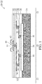
- FIG. 2 illustrates the application of dielectric layer 48 .
- the respective process is illustrated as process 206 in the process flow 200 as shown in FIG. 19 .
- dielectric layer 48 is formed of polymer diluted in a solvent.
- the formation of dielectric layer 48 may include spin-coating polymer layer 48 and pre-baking polymer layer 48 , so that it may maintain its shape in the subsequent light-exposure process and development process.
- the pre-baking is performed at a temperature in the range between about 100 degrees and about 180 degrees.
- the pre-baking duration may be in the range between about 2 minutes and about 10 minutes.
- N-Methyl-2-pyrrolidone which was conventional used as the solvent, is replaced by aliphatic amide, so that the desirable profile ( FIGS. 3 and 11 ) may be generated when openings are formed in dielectric layer 48 .
- the coated dielectric layer 48 (when and after it is coated but before baking) is free from NMP.
- the coated dielectric layer 48 (when and after it is coated but before baking), is substantially free from NMP, for example, including NMP with a weight percentage smaller than about 0.3 percent, or smaller than about 0.1 percent. It is appreciated that some analyzing equipment for detecting the composition of the polymer may detect the concentration of some chemicals such as NMP with concentrations higher than certain value such as 0.3 percent, but does not have the accuracy of detecting the NMP having concentrations lower than about 0.3 percent.
- the coated polymer 48 may also include other additives such as alkoxy decane.
- Alkoxy decane is also a polymer.
- the resulting polymer may include silicon alkoxide (with the formula Si(OR) n ), which may be detected using Fourier transform Infrared (FTIR) and Gas Chromatography Mass Spectrometry (GCMS).
- FTIR Fourier transform Infrared
- GCMS Gas Chromatography Mass Spectrometry
- the alkoxy decane in the coated dielectric layer 48 has a weight percentage greater than about 0.1 percent (excluding the solvent). The weight percentage of silicon alkoxide is detectable, and may be in the range between about 0.1 percent and about 10 percent.
- FIG. 2 also illustrates the light-exposure process of dielectric layer 48 , which is performed using lithography mask 50 .
- the respective process is illustrated as process 208 in the process flow 200 as shown in FIG. 19 .
- Lithography mask 50 includes opaque portions 50 A for blocking the light used in the light-exposure, and transparent portion 50 B allowing the light to pass through, so that selected portions of dielectric layer 48 are exposed.
- opening 52 is formed in dielectric layer 48 , as shown in FIG. 3 .
- the respective process is also illustrated as process 208 in the process flow 200 as shown in FIG. 19 .
- the top surface of metal pad 42 is exposed to opening 52 .
- a main baking process which is also a curing process, is performed to cure dielectric layer 48 .
- the respective process is illustrated as process 210 in the process flow 200 as shown in FIG. 19 .
- the main baking process is performed at a temperature in the range between about 200 degrees (° C.) and about 400 degrees.
- the main baking duration may be in the range between about 1 hour and about 12 hours. It is observed that the tilt angle ⁇ ( FIG. 11 ) is related to the baking temperature, and higher temperature results in greater tilt angle ⁇ , and vice versa. Accordingly, the baking temperature is adjusted in order to adjust tilt angle ⁇ .
- tilt angle ⁇ may be in the range greater than about 45 degrees and lower than about 90 degrees, which may be achieved through a pre-baking temperature in the range between about 120 degrees and about 210 degrees. Tilt angle ⁇ may also be in the range between about 70 degrees and about 80 degrees, which may be achieved through a pre-baking temperature in the range between about 140 degrees and about 160 degrees.
- the tilt angle ⁇ may be increased by increasing the exposure focus of the tool for the light-exposure process of dielectric layer 48 in accordance with some embodiments.
- the desirable tilt angle ⁇ may be achieved by adjusting the exposure focus to an appropriate value, which may be discovered through experiments.
- FIG. 11 illustrates a magnified view of opening 52 , which is filled with via portion 58 A of metal bump 58 in a subsequent process.
- dielectric layer 48 has a thickness H 1 , which is the thickness of a portion of dielectric layer 48 directly over metal pad 42 and passivation layer 44 .
- thickness H 1 is equal to or greater than about 5 ⁇ m, and may be in the range between about 5 ⁇ m and about 15 ⁇ m.
- adjusting thickness H 1 to be equal to or greater than about 5 ⁇ m is critical in reducing the stress in low-k dielectric layers 38 to a level that no cracks are generated in low-k dielectric layers 38 ( FIG. 3 ).
- Width W 1 is also the bottom width of opening 52 as shown in FIG. 3 .
- width W 1 is equal to or smaller than about 20 ⁇ m, and may be in the range between about 8 ⁇ m and about 20 ⁇ m.
- making width W 1 to be equal to or smaller than about 20 ⁇ m is critical in reducing the stress in low-k dielectric layers 38 to a level that no cracks are generated in low-k dielectric layers 38 .
- dielectric layer 48 has straight sidewalls 48 A, and round sidewalls 48 B connected to straight sidewalls 48 A.
- the round sidewalls 48 B are also connected to the top surface 42 A of metal pad 42 , which top surface also forms the bottom surface of opening 52 in FIG. 3 .
- the round sidewalls 48 B form parts of circles that have an R-angle, which is the diameter R of the respective circles to which round sidewalls 48 B fit.
- the R-angle is smaller than about 4 ⁇ m.
- the R-angle is greater than 0 ⁇ m, and may be greater than about 1 ⁇ m.
- the R-angle is in the range between about 1 ⁇ m and about 3 ⁇ m. As will be discussed in subsequent paragraphs, making the R-angle to be equal to or smaller than about 4 ⁇ m is critical in reducing the stress in low-k dielectric layers 38 to a level that no cracks are generated in low-k dielectric layers 38 .
- the straight sidewalls 48 A may have a tilt angle ⁇ , which is the sharp angle formed between straight sidewalls 48 A and a horizontal plane (which is parallel to a top surface and a bottom surface of package component 22 ).
- tilt angle ⁇ is in the range between about 45 degrees and about 90 degrees. As will be discussed in subsequent paragraphs, making the tilt angle ⁇ to be in the range between about 45 degrees and about 90 degrees is critical in reducing the stress in low-k dielectric layers 38 to a level that no cracks are generated in low-k dielectric layers 38 .
- the top surface 48 C of dielectric layer 48 may rise in the region where the top surface of dielectric layer 48 joins sidewalls 48 A. In the regions farther away from opening 52 , the top surfaces 48 C of dielectric layer 48 are planar.
- the rising-up height H 2 (also referred to as crown height) is smaller than 1.5 ⁇ m, and may be in the range between about 0.5 ⁇ m and about 1.5 ⁇ m.
- the rising surface 48 C is illustrated using dashed lines.
- the top surface of dielectric layer 48 also has the possibility of being planar in the region where the top surface of dielectric layer 48 joins sidewalls 48 A, as shown by solid lines in FIG. 4 (also shown in FIG. 3 ).
- the rising-up of the top surface is not shown in FIGS. 5 through 10 , although the top surfaces in these figures may also rise.
- FIGS. 5 through 9 illustrate the formation of a metal bump.
- the metal bump is formed to be in contact with metal pad 42 .
- additional conductive lines and possibly dielectric layers are formed over metal pad 42 and underlying the metal bump.
- RDLs Redistribution Lines
- PPIs Post-Passivation Interconnects
- seed layer 54 is deposited over dielectric layer 48 .
- Seed layer 54 is a conductive seed layer, and may be a metal seed layer in accordance with some embodiments.
- the respective process is illustrated as process 212 in the process flow 200 as shown in FIG. 19 .
- seed layer 54 is a composite layer comprising two or more layers.
- seed layer 54 may include a lower layer and an upper layer, wherein the lower layer may include a titanium layer, a titanium nitride layer, a tantalum layer, a tantalum nitride layer, or the like.
- the materials of the upper layer may include copper or a copper alloy.
- seed layer 54 is a single layer, which may be a copper layer, for example.
- Seed layer 54 may be formed using Physical Vapor Deposition (PVD), Plasma Enhanced CVD (PECVD), atomic layer deposition, etc., while other applicable methods may also be used.
- PVD Physical Vapor Deposition
- PECVD Plasma Enhanced CVD
- atomic layer deposition etc.
- Seed layer 54 is a conformal layer that extends into opening 52 .
- FIG. 6 illustrates the formation of a patterned plating mask 56 .
- the respective process is illustrated as process 214 in the process flow 200 as shown in FIG. 19 .
- plating mask 56 is formed of a photo resist.
- Plating mask 56 is patterned to form opening 58 , through which a portion of the seed layer 54 is exposed.
- the patterning of plating mask 56 may include a light-exposure process and a development process.
- Metal bump 58 may include one or a plurality of non-solder metal layers.
- metal bump 58 may include copper-containing layer 60 including copper or a copper alloy.
- Metal bump 58 may also include metal cap layer 62 over copper-containing layer 60 .
- Metal cap layer 62 may be a nickel-containing layer, a palladium-containing layer, a gold layer, and/or the like, or a composite layer comprising the aforementioned layers.
- solder region 64 is formed, for example, by plating.
- the respective process is also illustrated as process 216 in the process flow 200 as shown in FIG. 19 .
- Solder region 64 may be formed of a Sn—Ag alloy, a Sn—Ag—Cu alloy, or the like, and may be lead-free or lead-containing.
- plating mask 56 is removed in a stripping process, and the underlying portions of seed layer 54 are exposed.
- the respective process is illustrated as process 218 in the process flow 200 as shown in FIG. 19 .
- plating mask 56 may be ashed using oxygen.
- the exposed portions of seed layer 54 that were previously covered by plating mask 56 are removed through etching, for example, using sub-atmospheric-pressure pure hydrogen glow plasma to etch copper.
- the mixture of N 2 and H 2 or the mixture of Cl 2 and Ar may be used as the process gas.
- Titanium, if included in the seed layer, may be etched using a fluorine-containing gas such as SF 6 , or CF 4 , or NF 3 .
- the portions of seed layer 54 covered by metal bump 58 remain un-removed.
- the respective process is also illustrated as process 218 in the process flow 200 as shown in FIG. 19 .
- the resulting structure is shown in FIG. 8 .
- Metal bump 58 includes via portion 58 A extending into dielectric layer 48 , and bump portion 58 B higher than the top surface of dielectric layer 48 .
- the sidewalls of the bump portion 58 B of metal bump 58 may be substantially vertical and straight. The details of the profile of via portion 58 A may be found referring to the profile shown in FIG. 11 .
- solder region 64 is reflowed in a reflow process, for example, in a convection reflow process, laser reflow process, or the like.
- the respective process is illustrated as process 220 in the process flow 200 as shown in FIG. 19 .
- Solder region 64 thus has a rounded surface.
- FIG. 12 illustrates a top view of metal bump 58 .
- via portion 58 A and bump portion 58 B both have elongated shapes.
- the width W 1 (also refer to FIGS. 4 and 11 ) is the smaller width (in the widthwise direction) of via portion 58 A.
- metal bump 58 may have a non-elongated top view shape without a significant difference between the longer axis and shorter axis.
- the top-view shape may be a circular shape, and width W 1 is the diameter of the circular shape.
- the top-view shape via portion 58 A and bump portion 58 B of may also be hexagons, and width W 1 is the distance between two parallel edges of the corresponding hexagon.
- the shape of opening 46 ( FIG. 1 ) is also illustrated in FIG. 12 .
- wafer 20 is singulated in a die-saw process.
- the singulation is performed along scribe lines 66 .
- the respective process is illustrated as process 222 in the process flow 200 as shown in FIG. 19 .
- Package components 22 (which may be device dies, package substrate, interposers, packages, or the like) are thus separated from each other to form discrete package components.
- package component 68 which may be an interposer, a package substrate, a package, a device die, a printed circuit board, or the like.
- the respective process is illustrated as process 224 in the process flow 200 as shown in FIG. 19 .
- the bonding may be through solder region 65 , which includes the material of solder region 64 ( FIG. 9 ).
- Solder region 65 may or may not include additional solder from the solder region pre-formed on conductive feature 70 in package component 68 .
- Underfill 71 may be disposed into the gap between package component 22 and package component 68 .
- Underfill 71 may be in contact with the top surface of dielectric layer 48 , and may contact the sidewalls of bump portion 58 B. Furthermore, Underfill 71 may encircle, and may be in contact with, metal bump 58 . Package 72 is thus formed.
- FIG. 13 illustrates the simulation results, in which the stress in low-k dielectric layers 38 ( FIG. 10 ) is illustrated as a function of the width W 1 ( FIG. 11 ) of the via portion 58 A of the metal bump 58 .
- the X-axis represents the width W 1
- the Y-axis represents the stress in low-k dielectric layers 38 .
- FIG. 13 reveals that with the increase in the width W 1 , the stress in low-k dielectric layers 38 increases. When the width W 1 reaches about 20 ⁇ m or greater, the stress increases to the critical value of 150 MPa or higher.
- width W 1 is smaller than 20 ⁇ m, and has the possibility of cracking when width W 1 is greater than about 20 ⁇ m. Accordingly, reducing the width W 1 results in the desirable reduction in the stress in low-k dielectric layers 38 , and the width W 1 is designed to be smaller than about 20 ⁇ m.
- FIG. 14 illustrates the simulation results, wherein the normalized stress in low-k dielectric layers 38 ( FIG. 10 ) is illustrated as a function of the width W 1 ( FIG. 11 ) of the via portion 58 A.
- the X-axis represents the width W 1
- the Y-axis represents the normalized stress in low-k dielectric layers 38 , with the normalized stress being a ratio of the stress in dielectric layers 38 to the critical value of 150 MPa.
- FIG. 14 reveals that with the increase in the width W 1 , the stress in low-k dielectric layers 38 increases. When the width W 1 reaches about 20 ⁇ m, the normalized stress increases to 1.0.
- FIG. 14 also reveals that reducing the width W 1 results in the desirable reduction in the stress in low-k dielectric layers 38 , and the width W 1 is designed to be smaller than about 20 ⁇ m.
- FIG. 15 illustrates the simulation results, wherein the stress in low-k dielectric layers 38 ( FIG. 10 ) is illustrated as a function of the height H 1 ( FIG. 11 ) of the via portion 58 A of the metal bump 58 .
- the X-axis represents the height H 1 in microns
- the Y-axis represents the normalized stress in low-k dielectric layers 38 .
- FIG. 15 reveals that with the increase in the height H 1 , the stress in low-k dielectric layers 38 reduces.
- the height H 1 increases to about 5 ⁇ m or higher, the normalized stress reduces to the critical value of 1.0 or lower, which means that low-k dielectric layers 38 are unlikely to crack. Accordingly, increasing the height H 1 results in the desirable reduction in the stress in low-k dielectric layers 38 , and the height H 1 is designed to be greater than about 5 ⁇ m.
- FIG. 16 illustrates the simulation results, wherein the stress in low-k dielectric layers 38 ( FIG. 10 ) is illustrated as a function of the tilt angle ⁇ of the sidewalls 48 A ( FIG. 11 ) of the via portion 58 A.
- the X-axis represents the tilt angle ⁇
- the Y-axis represents the normalized stress in low-k dielectric layers 38 , which is normalized to the critical value of 150 MPa.
- FIG. 16 reveals that with the increase in the tilt angle ⁇ , the stress in low-k dielectric layers 38 reduces.
- the tilt angle ⁇ is greater than about 45 degrees, the normalized stress reduces to the critical value of 1.0, which means that low-k dielectric layers 38 will not crack.
- tilt angle ⁇ results in the desirable reduction in the stress in low-k dielectric layers 38 , and the tilt angle ⁇ is designed to be greater than about 45 degrees.
- the tilt angle ⁇ cannot be greater than 90 degrees since this will cause difficulty in forming a conformal seed layer 54 ( FIG. 5 ), which causes problems (such as voids) in the subsequent plating of metal bump 58 .
- tilt angle ⁇ is in the range between about 70 degrees and about 80 degrees.
- FIG. 17 illustrates the correlation of the R-angle and the tilt angle ⁇ .
- the X-axis represents the tilt angle ⁇
- the Y-axis represents the R-angle. It is found that with the increase in the tilt angle ⁇ , the R-angle reduces. As is aforementioned, reducing the tilt angle ⁇ and/or reducing the R-angle may reduce the stress in low-k dielectric layers 38 , and vice versa. Accordingly, FIG. 17 reveals that increasing the tilt angle ⁇ has similar effect as increasing the R-angle, and vice versa.
- the reduction of the stress in low-k dielectric layers 38 may be achieved through reducing the R-angle, reducing the width W 1 of the via portion of metal bump 58 , increasing the thickness H 1 of dielectric layer 48 , and increasing the tilt angle ⁇ .
- Simulation results have revealed that when the width W 1 ( FIG. 11 ) is smaller than about 20 ⁇ m, the height H 1 is greater than about 5 ⁇ m, and the tilt angle is greater than about 45 degrees (and smaller than 90 degrees), no crack will be resulted in the low-k dielectric layers by the stress applied by the metal bump 58 and dielectric layer 48 .
- FIG. 18 illustrates a relationship between tilt angle ⁇ and the exposure focus for performing the light exposure on dielectric layer 48 (when dielectric layer 48 is a light-sensitive layer) in the process shown in FIG. 2 . It is appreciated that FIG. 18 illustrates an example, and the relationship may be different when different exposure tool is used. As shown in FIG. 18 , the profile angle may be increased by increasing the exposure focus in accordance with some embodiments.
- the embodiments of the present disclosure have some advantageous features.
- the profile of the via portion of the metal bump which profile includes the bottom width W 1 of the via portion of the metal bump, the thickness of the polymer, and the tilt angle ⁇ of the sidewall of the via portion of the metal bump, is adjusted to the desired profile, so that the stress in the underlying low-k dielectric layers is reduced, and the cracking in the low-k dielectric layers is avoided.
- a method of forming an integrated circuit structure comprises forming a patterned passivation layer over a metal pad, with a top surface of the metal pad revealed through a first opening in the patterned passivation layer; applying a polymer layer over the patterned passivation layer, wherein the polymer layer is substantially free from NMP, and wherein the polymer layer comprises aliphatic amide as a solvent; performing a light-exposure process on the polymer layer; performing a development process on the polymer layer to form a second opening in the polymer layer, wherein the top surface of the metal pad is revealed to the second opening; baking the polymer; and forming a conductive region comprising a via portion extending into the second opening.
- the polymer layer comprises alkoxy decane.
- the via portion comprise a straight sidewall; a straight bottom surface; and a round corner comprising a top end connecting to the straight sidewall, and a bottom end connecting to the straight bottom surface, wherein the round corner has an R-angle smaller than about 4 ⁇ m.
- the straight sidewall has a tilt angle in a range between about 45 degrees and about 90 degrees.
- the straight sidewall has a tilt angle in a range between about 70 degrees and about 80 degrees.
- the polymer layer after the baking process, has a thickness greater than about 5 ⁇ m.
- the NMP has a weight percentage smaller than about 0.3 percent in the polymer layer.
- the polymer layer is free from NMP.
- a method of forming an integrated circuit structure comprises applying a polymer layer over a metal pad; patterning the polymer layer to form an opening in the polymer layer, wherein a top surface of the metal pad is revealed to the opening, and the polymer layer comprises: a straight sidewall facing the opening; and a round corner surface comprising a top end connecting to the straight sidewall, and a bottom end joining to the top surface of the metal pad, wherein the round corner surface has an R-angle smaller than about 4 ⁇ m; and forming a conductive region comprising: a via portion extending into the opening; and a bump portion over the polymer layer.
- the polymer layer when applied, comprises aliphatic amide as a solvent.
- the polymer layer when applied, is free from NMP.
- the polymer layer comprises silicon alkoxide.
- the method further includes baking the polymer layer after the polymer layer is patterned.
- an integrated circuit structure comprises a metal pad; a polymer layer over and contacting the metal pad; and a metal bump comprising a via portion in the polymer layer, wherein the via portion comprises: a straight sidewall; a straight bottom surface; and a round bottom corner comprising a top end connecting to the straight sidewall, and a bottom end connecting to the straight bottom surface, wherein the round bottom corner has an R-angle smaller than about 4 ⁇ m; and a bump portion over the polymer layer and joining to the via portion.
- the straight sidewall has a tilt angle in a range between about 45 degrees and about 90 degrees. In an embodiment, the tilt angle is in a range between about 70 degrees and about 80 degrees.
- the polymer layer comprises silicon alkoxide.
- a portion of the polymer layer directly over the metal pad has a thickness greater than about 5 ⁇ m.
- the via portion contacts a top surface of the metal pad to form an interface, and the interface has a width smaller than about 20 ⁇ m.
Abstract
Description
R-angle=0.0152θ2−0.5863θ+4.3865 [Eq. 1]
Claims (18)
Priority Applications (6)
| Application Number | Priority Date | Filing Date | Title |
|---|---|---|---|
| US16/458,719 US11024593B2 (en) | 2018-09-28 | 2019-07-01 | Metal bumps and method forming same |
| DE102019118478.9A DE102019118478A1 (en) | 2018-09-28 | 2019-07-09 | METAL BUMPER AND METHOD FOR MAKING SAME |
| KR1020190105794A KR102324013B1 (en) | 2018-09-28 | 2019-08-28 | Metal bumps and method forming same |
| CN201910925482.4A CN110970311B (en) | 2018-09-28 | 2019-09-27 | Integrated circuit structure and method of forming an integrated circuit structure |
| TW108135089A TWI739163B (en) | 2018-09-28 | 2019-09-27 | Integrated circuit structure and method forming same |
| US17/333,187 US20210288009A1 (en) | 2018-09-28 | 2021-05-28 | Metal Bumps and Method Forming Same |
Applications Claiming Priority (2)
| Application Number | Priority Date | Filing Date | Title |
|---|---|---|---|
| US201862738511P | 2018-09-28 | 2018-09-28 | |
| US16/458,719 US11024593B2 (en) | 2018-09-28 | 2019-07-01 | Metal bumps and method forming same |
Related Child Applications (1)
| Application Number | Title | Priority Date | Filing Date |
|---|---|---|---|
| US17/333,187 Division US20210288009A1 (en) | 2018-09-28 | 2021-05-28 | Metal Bumps and Method Forming Same |
Publications (2)
| Publication Number | Publication Date |
|---|---|
| US20200105696A1 US20200105696A1 (en) | 2020-04-02 |
| US11024593B2 true US11024593B2 (en) | 2021-06-01 |
Family
ID=69945064
Family Applications (2)
| Application Number | Title | Priority Date | Filing Date |
|---|---|---|---|
| US16/458,719 Active US11024593B2 (en) | 2018-09-28 | 2019-07-01 | Metal bumps and method forming same |
| US17/333,187 Pending US20210288009A1 (en) | 2018-09-28 | 2021-05-28 | Metal Bumps and Method Forming Same |
Family Applications After (1)
| Application Number | Title | Priority Date | Filing Date |
|---|---|---|---|
| US17/333,187 Pending US20210288009A1 (en) | 2018-09-28 | 2021-05-28 | Metal Bumps and Method Forming Same |
Country Status (4)
| Country | Link |
|---|---|
| US (2) | US11024593B2 (en) |
| KR (1) | KR102324013B1 (en) |
| CN (1) | CN110970311B (en) |
| TW (1) | TWI739163B (en) |
Families Citing this family (3)
| Publication number | Priority date | Publication date | Assignee | Title |
|---|---|---|---|---|
| CN113363160A (en) * | 2020-05-27 | 2021-09-07 | 台湾积体电路制造股份有限公司 | Semiconductor device and method of forming the same |
| US20220037248A1 (en) * | 2020-07-31 | 2022-02-03 | Samsung Electronics Co., Ltd. | Semiconductor packages |
| CN117276452A (en) * | 2022-03-24 | 2023-12-22 | 深圳市广社照明科技有限公司 | Insulating adhesive base conductive device and manufacturing method thereof |
Citations (33)
| Publication number | Priority date | Publication date | Assignee | Title |
|---|---|---|---|---|
| US20040053483A1 (en) * | 2002-06-25 | 2004-03-18 | Nair Krishna K. | Methods of forming electronic structures including conductive shunt layers and related structures |
| US7348210B2 (en) * | 2005-04-27 | 2008-03-25 | International Business Machines Corporation | Post bump passivation for soft error protection |
| US7569937B2 (en) * | 2005-07-29 | 2009-08-04 | Advanced Micro Devices, Inc. | Technique for forming a copper-based contact layer without a terminal metal |
| US7838424B2 (en) | 2007-07-03 | 2010-11-23 | Taiwan Semiconductor Manufacturing Company, Ltd. | Enhanced reliability of wafer-level chip-scale packaging (WLCSP) die separation using dry etching |
| US7863742B2 (en) | 2007-11-01 | 2011-01-04 | Taiwan Semiconductor Manufacturing Company, Ltd. | Back end integrated WLCSP structure without aluminum pads |
| US7932601B2 (en) | 2007-05-29 | 2011-04-26 | Taiwan Semiconductor Manufacturing Company, Ltd. | Enhanced copper posts for wafer level chip scale packaging |
| US20110101527A1 (en) * | 2009-11-05 | 2011-05-05 | Taiwan Semiconductor Manufacturing Company, Ltd. | Mechanisms for forming copper pillar bumps |
| US20110254151A1 (en) * | 2010-04-16 | 2011-10-20 | Taiwan Semiconductor Manufacturing Company, Ltd. | Method for fabricating bump structure without ubm undercut |
| US20120181686A1 (en) | 2011-01-19 | 2012-07-19 | Samsung Electronics Co., Ltd. | Method of preparing semiconductor package and semiconductor die for semiconductor package |
| US20120319251A1 (en) | 2011-06-16 | 2012-12-20 | Taiwan Semiconductor Manufacturing Company, Ltd. | Solder Ball Protection Structure with Thick Polymer Layer |
| TW201322379A (en) | 2011-11-18 | 2013-06-01 | Chipmos Technologies Inc | Conductive structure and method for forming the same |
| US8592300B2 (en) * | 2009-12-08 | 2013-11-26 | Taiwan Semiconductor Manufacturing Company, Ltd. | Interface structure for copper-copper peeling integrity |
| US20130341800A1 (en) | 2012-06-21 | 2013-12-26 | Taiwan Semiconductor Manufacturing Company, Ltd. | Integrated Circuit Packages and Methods for Forming the Same |
| US20140015122A1 (en) | 2012-07-11 | 2014-01-16 | Taiwan Semiconductor Manufacturing Company, Ltd. | Method of Forming Post Passivation Interconnects |
| US20140045379A1 (en) | 2012-08-08 | 2014-02-13 | Taiwan Semiconductor Manufacturing Company, Ltd. | Package Assembly and Methods for Forming the Same |
| US20140048926A1 (en) | 2012-08-14 | 2014-02-20 | Taiwan Semiconductor Manufacturing Company, Ltd. | Semiconductor package and method of manufacturing the same |
| US20140077356A1 (en) | 2012-09-14 | 2014-03-20 | Taiwan Semiconductor Manufacturing Company, Ltd. | Post Passivation Interconnect Structures and Methods for Forming the Same |
| US8754508B2 (en) | 2012-08-29 | 2014-06-17 | Taiwan Semiconductor Manufacturing Company, Ltd. | Structure to increase resistance to electromigration |
| US20140183693A1 (en) | 2012-12-27 | 2014-07-03 | Taiwan Semiconductor Manufacturing Company, Ltd. | Capacitor in Post-Passivation Structures and Methods of Forming the Same |
| US20140187103A1 (en) | 2012-12-28 | 2014-07-03 | Taiwan Semiconductor Manufacturing Company, Ltd. | System and Method for an Improved Fine Pitch Joint |
| US8772151B2 (en) | 2012-09-27 | 2014-07-08 | Taiwan Semiconductor Manufacturing Company, Ltd. | Passivation scheme |
| CN103915374A (en) | 2013-01-09 | 2014-07-09 | 台湾积体电路制造股份有限公司 | Post-passivation interconnect structure and methods for forming the same |
| US20140252558A1 (en) | 2013-03-11 | 2014-09-11 | Taiwan Semiconductor Manufacturing Company, Ltd. | Methods and Apparatus for Wafer Level Packaging |
| US20140252601A1 (en) | 2013-03-11 | 2014-09-11 | Taiwan Semiconductor Manufacturing Company, Ltd. | Interconnect Structures and Methods of Forming Same |
| US20140252597A1 (en) | 2013-03-08 | 2014-09-11 | Taiwan Semiconductor Manufacturing Company, Ltd. | Directly Sawing Wafers Covered with Liquid Molding Compound |
| US20140252608A1 (en) | 2013-03-06 | 2014-09-11 | Taiwan Semiconductor Manufacturing Company, Ltd. | Method and Apparatus for Packaging Pad Structure |
| US20140262468A1 (en) | 2013-03-12 | 2014-09-18 | Taiwan Semiconductor Manufacturing Company, Ltd. | System and Method for an Improved Interconnect Structure |
| US20140264885A1 (en) | 2013-03-12 | 2014-09-18 | Taiwan Semiconductor Manufacturing Company, Ltd. | Apparatus and Method for Wafer Separation |
| KR20150070215A (en) | 2012-10-11 | 2015-06-24 | 닛산 가가쿠 고교 가부시키 가이샤 | Coating liquid for forming inorganic oxide coating film, inorganic oxide coating film, and display device |
| US20150228587A1 (en) * | 2014-02-13 | 2015-08-13 | Taiwan Semiconductor Manufacturing Company, Ltd. | Concentric Bump Design for the Alignment in Die Stacking |
| US20150228600A1 (en) * | 2014-02-07 | 2015-08-13 | Taiwan Semiconductor Manufacturing Company, Ltd. | Packages with stress-reducing structures and methods of forming same |
| US9922896B1 (en) * | 2016-09-16 | 2018-03-20 | Taiwan Semiconductor Manufacturing Company, Ltd. | Info structure with copper pillar having reversed profile |
| TW201826023A (en) | 2016-09-08 | 2018-07-16 | 日商住友電木股份有限公司 | Method of manufacturing semiconductor device |
Family Cites Families (6)
| Publication number | Priority date | Publication date | Assignee | Title |
|---|---|---|---|---|
| TW421670B (en) * | 1999-04-02 | 2001-02-11 | Ind Tech Res Inst | Fast-cured sol materials |
| JP2005026363A (en) * | 2003-06-30 | 2005-01-27 | Toshiba Corp | Semiconductor device and its manufacturing method |
| TWI223363B (en) * | 2003-11-06 | 2004-11-01 | Ind Tech Res Inst | Bonding structure with compliant bumps |
| US7678682B2 (en) * | 2004-11-12 | 2010-03-16 | Axcelis Technologies, Inc. | Ultraviolet assisted pore sealing of porous low k dielectric films |
| US7759792B2 (en) * | 2007-08-15 | 2010-07-20 | Infineon Technologies Ag | Integrated circuit including parylene material layer |
| US9111817B2 (en) * | 2012-09-18 | 2015-08-18 | Taiwan Semiconductor Manufacturing Company, Ltd. | Bump structure and method of forming same |
-
2019
- 2019-07-01 US US16/458,719 patent/US11024593B2/en active Active
- 2019-08-28 KR KR1020190105794A patent/KR102324013B1/en active IP Right Grant
- 2019-09-27 CN CN201910925482.4A patent/CN110970311B/en active Active
- 2019-09-27 TW TW108135089A patent/TWI739163B/en active
-
2021
- 2021-05-28 US US17/333,187 patent/US20210288009A1/en active Pending
Patent Citations (41)
| Publication number | Priority date | Publication date | Assignee | Title |
|---|---|---|---|---|
| US20040053483A1 (en) * | 2002-06-25 | 2004-03-18 | Nair Krishna K. | Methods of forming electronic structures including conductive shunt layers and related structures |
| US7348210B2 (en) * | 2005-04-27 | 2008-03-25 | International Business Machines Corporation | Post bump passivation for soft error protection |
| US7569937B2 (en) * | 2005-07-29 | 2009-08-04 | Advanced Micro Devices, Inc. | Technique for forming a copper-based contact layer without a terminal metal |
| US7932601B2 (en) | 2007-05-29 | 2011-04-26 | Taiwan Semiconductor Manufacturing Company, Ltd. | Enhanced copper posts for wafer level chip scale packaging |
| US7838424B2 (en) | 2007-07-03 | 2010-11-23 | Taiwan Semiconductor Manufacturing Company, Ltd. | Enhanced reliability of wafer-level chip-scale packaging (WLCSP) die separation using dry etching |
| US7863742B2 (en) | 2007-11-01 | 2011-01-04 | Taiwan Semiconductor Manufacturing Company, Ltd. | Back end integrated WLCSP structure without aluminum pads |
| US20110101527A1 (en) * | 2009-11-05 | 2011-05-05 | Taiwan Semiconductor Manufacturing Company, Ltd. | Mechanisms for forming copper pillar bumps |
| US8592300B2 (en) * | 2009-12-08 | 2013-11-26 | Taiwan Semiconductor Manufacturing Company, Ltd. | Interface structure for copper-copper peeling integrity |
| US20110254151A1 (en) * | 2010-04-16 | 2011-10-20 | Taiwan Semiconductor Manufacturing Company, Ltd. | Method for fabricating bump structure without ubm undercut |
| US20120181686A1 (en) | 2011-01-19 | 2012-07-19 | Samsung Electronics Co., Ltd. | Method of preparing semiconductor package and semiconductor die for semiconductor package |
| KR20120084194A (en) | 2011-01-19 | 2012-07-27 | 삼성전자주식회사 | Method for preparing semiconductor package and die for semiconductor package |
| US20120319251A1 (en) | 2011-06-16 | 2012-12-20 | Taiwan Semiconductor Manufacturing Company, Ltd. | Solder Ball Protection Structure with Thick Polymer Layer |
| US20150011082A1 (en) | 2011-11-18 | 2015-01-08 | Chipmos Technologies Inc. | Conductive structure and method for forming the same |
| TW201322379A (en) | 2011-11-18 | 2013-06-01 | Chipmos Technologies Inc | Conductive structure and method for forming the same |
| US20130341800A1 (en) | 2012-06-21 | 2013-12-26 | Taiwan Semiconductor Manufacturing Company, Ltd. | Integrated Circuit Packages and Methods for Forming the Same |
| US20140015122A1 (en) | 2012-07-11 | 2014-01-16 | Taiwan Semiconductor Manufacturing Company, Ltd. | Method of Forming Post Passivation Interconnects |
| US20140045379A1 (en) | 2012-08-08 | 2014-02-13 | Taiwan Semiconductor Manufacturing Company, Ltd. | Package Assembly and Methods for Forming the Same |
| US20140048926A1 (en) | 2012-08-14 | 2014-02-20 | Taiwan Semiconductor Manufacturing Company, Ltd. | Semiconductor package and method of manufacturing the same |
| US8754508B2 (en) | 2012-08-29 | 2014-06-17 | Taiwan Semiconductor Manufacturing Company, Ltd. | Structure to increase resistance to electromigration |
| US20140077356A1 (en) | 2012-09-14 | 2014-03-20 | Taiwan Semiconductor Manufacturing Company, Ltd. | Post Passivation Interconnect Structures and Methods for Forming the Same |
| US8772151B2 (en) | 2012-09-27 | 2014-07-08 | Taiwan Semiconductor Manufacturing Company, Ltd. | Passivation scheme |
| CN104854509A (en) | 2012-10-11 | 2015-08-19 | 日产化学工业株式会社 | Coating liquid for forming inorganic oxide coating film, inorganic oxide coating film, and display device |
| KR20150070215A (en) | 2012-10-11 | 2015-06-24 | 닛산 가가쿠 고교 가부시키 가이샤 | Coating liquid for forming inorganic oxide coating film, inorganic oxide coating film, and display device |
| US20140183693A1 (en) | 2012-12-27 | 2014-07-03 | Taiwan Semiconductor Manufacturing Company, Ltd. | Capacitor in Post-Passivation Structures and Methods of Forming the Same |
| US20140187103A1 (en) | 2012-12-28 | 2014-07-03 | Taiwan Semiconductor Manufacturing Company, Ltd. | System and Method for an Improved Fine Pitch Joint |
| US8846548B2 (en) | 2013-01-09 | 2014-09-30 | Taiwan Semiconductor Manufacturing Company, Ltd. | Post-passivation interconnect structure and methods for forming the same |
| CN103915374A (en) | 2013-01-09 | 2014-07-09 | 台湾积体电路制造股份有限公司 | Post-passivation interconnect structure and methods for forming the same |
| US20140252608A1 (en) | 2013-03-06 | 2014-09-11 | Taiwan Semiconductor Manufacturing Company, Ltd. | Method and Apparatus for Packaging Pad Structure |
| US20140252597A1 (en) | 2013-03-08 | 2014-09-11 | Taiwan Semiconductor Manufacturing Company, Ltd. | Directly Sawing Wafers Covered with Liquid Molding Compound |
| US20140252601A1 (en) | 2013-03-11 | 2014-09-11 | Taiwan Semiconductor Manufacturing Company, Ltd. | Interconnect Structures and Methods of Forming Same |
| US20140252558A1 (en) | 2013-03-11 | 2014-09-11 | Taiwan Semiconductor Manufacturing Company, Ltd. | Methods and Apparatus for Wafer Level Packaging |
| US20140262468A1 (en) | 2013-03-12 | 2014-09-18 | Taiwan Semiconductor Manufacturing Company, Ltd. | System and Method for an Improved Interconnect Structure |
| US20140264885A1 (en) | 2013-03-12 | 2014-09-18 | Taiwan Semiconductor Manufacturing Company, Ltd. | Apparatus and Method for Wafer Separation |
| US20150228600A1 (en) * | 2014-02-07 | 2015-08-13 | Taiwan Semiconductor Manufacturing Company, Ltd. | Packages with stress-reducing structures and methods of forming same |
| US20150228587A1 (en) * | 2014-02-13 | 2015-08-13 | Taiwan Semiconductor Manufacturing Company, Ltd. | Concentric Bump Design for the Alignment in Die Stacking |
| TW201826023A (en) | 2016-09-08 | 2018-07-16 | 日商住友電木股份有限公司 | Method of manufacturing semiconductor device |
| US9922896B1 (en) * | 2016-09-16 | 2018-03-20 | Taiwan Semiconductor Manufacturing Company, Ltd. | Info structure with copper pillar having reversed profile |
| US20180082917A1 (en) | 2016-09-16 | 2018-03-22 | Taiwan Semiconductor Manufacturing Company, Ltd. | Info structure with copper pillar having reversed profile |
| CN107833837A (en) | 2016-09-16 | 2018-03-23 | 台湾积体电路制造股份有限公司 | The message structure of copper post with reverse profile |
| TW201826408A (en) | 2016-09-16 | 2018-07-16 | 台灣積體電路製造股份有限公司 | Info structure with copper pillar having reversed profile |
| US10290530B2 (en) | 2016-09-16 | 2019-05-14 | Taiwan Semiconductor Manufacturing Company, Ltd. | Info structure with copper pillar having reversed profile |
Also Published As
| Publication number | Publication date |
|---|---|
| TWI739163B (en) | 2021-09-11 |
| KR20200037075A (en) | 2020-04-08 |
| US20200105696A1 (en) | 2020-04-02 |
| CN110970311A (en) | 2020-04-07 |
| CN110970311B (en) | 2022-08-05 |
| KR102324013B1 (en) | 2021-11-10 |
| TW202025320A (en) | 2020-07-01 |
| US20210288009A1 (en) | 2021-09-16 |
Similar Documents
| Publication | Publication Date | Title |
|---|---|---|
| US10854574B2 (en) | Forming metal bonds with recesses | |
| US11094671B2 (en) | Package with thinned substrate | |
| US20210288009A1 (en) | Metal Bumps and Method Forming Same | |
| US11670609B2 (en) | Method for manufacturing a semiconductor device including patterning a polymer layer to reduce stress | |
| US20220367397A1 (en) | Metal-Bump Sidewall Protection | |
| CN106601622B (en) | Bonding structure and method for forming the same | |
| US10629477B2 (en) | Raised via for terminal connections on different planes | |
| US9576929B1 (en) | Multi-strike process for bonding | |
| US11450567B2 (en) | Package component with stepped passivation layer | |
| US20240021509A1 (en) | Multi-Liner TSV Structure and Method Forming Same | |
| US20210375672A1 (en) | Redistribution Lines Having Nano Columns and Method Forming Same | |
| US11387143B2 (en) | Redistribution lines with protection layers and method forming same | |
| US11961762B2 (en) | Package component with stepped passivation layer | |
| US20220336276A1 (en) | Package Component with Stepped Passivation Layer | |
| US20220384259A1 (en) | Semiconductor Structure with Pull-in Planarization Layer and Method Forming the Same | |
| US11721579B2 (en) | Redistribution lines with protection layers and method forming same | |
| US20230275047A1 (en) | Shifting Contact Pad for Reducing Stress |
Legal Events
| Date | Code | Title | Description |
|---|---|---|---|
| AS | Assignment |
Owner name: TAIWAN SEMICONDUCTOR MANUFACTURING COMPANY, LTD., TAIWAN Free format text: ASSIGNMENT OF ASSIGNORS INTEREST;ASSIGNORS:CHENG, MING-DA;CHAO, YUNG-CHING;TZENG, CHUN KAI;AND OTHERS;SIGNING DATES FROM 20190618 TO 20190624;REEL/FRAME:049642/0771 |
|
| FEPP | Fee payment procedure |
Free format text: ENTITY STATUS SET TO UNDISCOUNTED (ORIGINAL EVENT CODE: BIG.); ENTITY STATUS OF PATENT OWNER: LARGE ENTITY |
|
| STPP | Information on status: patent application and granting procedure in general |
Free format text: NON FINAL ACTION MAILED |
|
| STPP | Information on status: patent application and granting procedure in general |
Free format text: RESPONSE TO NON-FINAL OFFICE ACTION ENTERED AND FORWARDED TO EXAMINER |
|
| STPP | Information on status: patent application and granting procedure in general |
Free format text: NON FINAL ACTION MAILED |
|
| STPP | Information on status: patent application and granting procedure in general |
Free format text: NOTICE OF ALLOWANCE MAILED -- APPLICATION RECEIVED IN OFFICE OF PUBLICATIONS |
|
| AS | Assignment |
Owner name: TAIWAN SEMICONDUCTOR MANUFACTURING CO., LTD., TAIWAN Free format text: CORRECTIVE ASSIGNMENT TO CORRECT THE TYPOGRAPHICAL ERROR IN THE 4TH AND 5TH INVENTORS NAME PREVIOUSLY RECORDED ON REEL 049642 FRAME 0771. ASSIGNOR(S) HEREBY CONFIRMS THE ASSIGNMENT OF ASSIGNOR'S INTEREST;ASSIGNORS:CHENG, MING-DA;CHAO, YUNG-CHING;TZENG, CHUN KAI;AND OTHERS;SIGNING DATES FROM 20201119 TO 20210219;REEL/FRAME:055403/0080 |
|
| STPP | Information on status: patent application and granting procedure in general |
Free format text: PUBLICATIONS -- ISSUE FEE PAYMENT VERIFIED |
|
| STPP | Information on status: patent application and granting procedure in general |
Free format text: AWAITING TC RESP, ISSUE FEE PAYMENT VERIFIED |
|
| STPP | Information on status: patent application and granting procedure in general |
Free format text: PUBLICATIONS -- ISSUE FEE PAYMENT VERIFIED |
|
| STCF | Information on status: patent grant |
Free format text: PATENTED CASE |