WO2018042881A1 - 半導体装置 - Google Patents
半導体装置 Download PDFInfo
- Publication number
- WO2018042881A1 WO2018042881A1 PCT/JP2017/024911 JP2017024911W WO2018042881A1 WO 2018042881 A1 WO2018042881 A1 WO 2018042881A1 JP 2017024911 W JP2017024911 W JP 2017024911W WO 2018042881 A1 WO2018042881 A1 WO 2018042881A1
- Authority
- WO
- WIPO (PCT)
- Prior art keywords
- transistor
- temperature
- active clamp
- semiconductor device
- circuit
- Prior art date
- Legal status (The legal status is an assumption and is not a legal conclusion. Google has not performed a legal analysis and makes no representation as to the accuracy of the status listed.)
- Ceased
Links
Images






Classifications
-
- H—ELECTRICITY
- H03—ELECTRONIC CIRCUITRY
- H03K—PULSE TECHNIQUE
- H03K17/00—Electronic switching or gating, i.e. not by contact-making and –breaking
- H03K17/08—Modifications for protecting switching circuit against overcurrent or overvoltage
- H03K17/082—Modifications for protecting switching circuit against overcurrent or overvoltage by feedback from the output to the control circuit
- H03K17/0822—Modifications for protecting switching circuit against overcurrent or overvoltage by feedback from the output to the control circuit in field-effect transistor switches
-
- H—ELECTRICITY
- H03—ELECTRONIC CIRCUITRY
- H03K—PULSE TECHNIQUE
- H03K17/00—Electronic switching or gating, i.e. not by contact-making and –breaking
- H03K17/08—Modifications for protecting switching circuit against overcurrent or overvoltage
- H03K17/081—Modifications for protecting switching circuit against overcurrent or overvoltage without feedback from the output circuit to the control circuit
- H03K17/0814—Modifications for protecting switching circuit against overcurrent or overvoltage without feedback from the output circuit to the control circuit by measures taken in the output circuit
-
- H—ELECTRICITY
- H10—SEMICONDUCTOR DEVICES; ELECTRIC SOLID-STATE DEVICES NOT OTHERWISE PROVIDED FOR
- H10D—INORGANIC ELECTRIC SEMICONDUCTOR DEVICES
- H10D84/00—Integrated devices formed in or on semiconductor substrates that comprise only semiconducting layers, e.g. on Si wafers or on GaAs-on-Si wafers
- H10D84/01—Manufacture or treatment
- H10D84/02—Manufacture or treatment characterised by using material-based technologies
- H10D84/03—Manufacture or treatment characterised by using material-based technologies using Group IV technology, e.g. silicon technology or silicon-carbide [SiC] technology
- H10D84/038—Manufacture or treatment characterised by using material-based technologies using Group IV technology, e.g. silicon technology or silicon-carbide [SiC] technology using silicon technology, e.g. SiGe
-
- H—ELECTRICITY
- H10—SEMICONDUCTOR DEVICES; ELECTRIC SOLID-STATE DEVICES NOT OTHERWISE PROVIDED FOR
- H10D—INORGANIC ELECTRIC SEMICONDUCTOR DEVICES
- H10D89/00—Aspects of integrated devices not covered by groups H10D84/00 - H10D88/00
- H10D89/60—Integrated devices comprising arrangements for electrical or thermal protection, e.g. protection circuits against electrostatic discharge [ESD]
- H10D89/601—Integrated devices comprising arrangements for electrical or thermal protection, e.g. protection circuits against electrostatic discharge [ESD] for devices having insulated gate electrodes, e.g. for IGFETs or IGBTs
-
- H—ELECTRICITY
- H03—ELECTRONIC CIRCUITRY
- H03K—PULSE TECHNIQUE
- H03K17/00—Electronic switching or gating, i.e. not by contact-making and –breaking
- H03K17/08—Modifications for protecting switching circuit against overcurrent or overvoltage
- H03K2017/0806—Modifications for protecting switching circuit against overcurrent or overvoltage against excessive temperature
Definitions
- the present invention relates to a semiconductor device.
- a semiconductor device that constitutes a drive circuit such as a solenoid load mounted in an in-vehicle ECU (Electrical Control Unit) has a high breakdown voltage of 30 V or more and a high current drive capability of an amperage, as well as malfunction and element destruction of the power transistor. It is required to absorb the current energy generated at the output terminal so as not to occur. For this reason, there is a method of providing active clamp circuits at the gate and drain of the power transistor in the output stage (see, for example, Patent Document 1). As a result, current energy generated at the output terminal can be released to the ground.
- the current energy (thermal breakdown energy) that can be consumed by the power transistor during the active clamp operation is determined by the conditions of thermal runaway due to self-heating of the transistor, and generally increases the value by increasing the transistor size. Can do. However, an increase in transistor size has a problem of increasing the chip cost.
- a technique for making the temperature distribution in the transistor uniform is disclosed.
- One is to increase the interval between the active regions of the transistors arranged in parallel in the central region and to reduce it in the peripheral region (see, for example, Patent Document 2), and the other is to reduce the input power in the central region to the periphery.
- This is a method of reducing the input power of the area. Both methods can reduce the power consumption per unit area from the peripheral region toward the central region, thereby making the temperature distribution in the transistor uniform and, as a result, increasing the thermal breakdown energy of the transistor. Can do.
- the semiconductor integrated circuit having an overtemperature detection circuit that detects whether the temperature of the power transistor is equal to or higher than a predetermined temperature.
- the transistor is not driven and the first A technique for bringing a power transistor into an active clamp state with a second clamp voltage lower than the clamp voltage is disclosed (see, for example, Patent Document 4). Since the surge energy consumption time can be lengthened to suppress the rapid temperature rise of the transistor, the temperature setting for detecting overtemperature can be brought close to the maximum guaranteed operating temperature. As a result, the transistor can be operated at a higher temperature.
- the active region spacing between the central region transistor and the peripheral region transistor is such that the power consumption density of the transistor decreases from the peripheral region toward the central region. And changing the shape. For this reason, there is a problem that the performance per area of the transistor is lowered in the central region during normal operation. In addition, since it is necessary to change the transistor shape, there is a problem that the structure design of the transistor becomes complicated.
- Patent Document 3 can improve the uniformity of the transistor temperature, but in order to make the current performance of the transistor in the normal operation the same, compared with the case where no inactive region is provided. There is a problem that the size of the transistor is increased by an amount corresponding to the inactive region.
- An object of the present invention is to provide a semiconductor device capable of improving the uniformity of transistor temperature in an active clamp state while maintaining current performance.
- the present invention provides a first transistor having a first control electrode, a second transistor connected in parallel to the first transistor and having a second control electrode, the first transistor, and the first transistor.
- An active clamp circuit that is provided in a first path from a first connection point between two transistors to the first control electrode, and that conducts when a voltage at the first connection point exceeds a first threshold;
- An active clamp cutoff circuit provided in a second path from the clamp circuit to the second control electrode, and blocking or suppressing a current flowing through the second path.
- FIG. 1 is a circuit diagram of a load driving circuit according to a first embodiment.
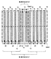
- FIG. FIG. 2 is a plan view of the power transistor shown in FIG. 1. It is a figure which shows the time transition of the temperature in a transistor at the time of active clamp operation
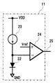
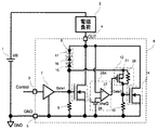
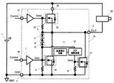
- FIG. 2 is a circuit diagram of a temperature detection circuit shown in FIG. 1. It is a circuit diagram of the load drive circuit by 2nd Embodiment. It is a circuit diagram of the load drive circuit by 3rd Embodiment. It is a circuit diagram of the load drive circuit by 4th Embodiment.
- the load driving circuit semiconductor device
- the same numerals indicate the same parts.
- the load driving circuit according to the embodiment of the present invention partially overlaps with the above-described object, but, for example, is intended to achieve the following first and second objects.
- the first object is to improve the uniformity of the transistor temperature during active clamping without increasing the transistor size and without reducing the current performance per area of the transistor during normal operation. This is to increase the thermal breakdown energy and the allowable energy for preventing the transistor from exceeding the rated temperature.
- the second object is to improve the uniformity of the transistor temperature during the active clamp operation without increasing the active clamp time, thereby enabling the transistor to operate in a higher temperature environment. It is in.
- the Zener diodes 15 and 16 are avalanche breakdown, A current flows through the active clamp circuit 8 and a current flows through the gate resistor 9 connected between the source and gate of the power transistor 29 to turn on the power transistor 29 (active clamp operation). As a result, the current energy generated at the output terminal 4 can be released to the ground.
- FIG. 1 is a circuit diagram of a load driving circuit 6 (semiconductor device) according to the first embodiment.
- the load driving circuit 6 includes a power transistor 13 composed of a first group of MOSFETs (semiconductor elements) formed on a semiconductor substrate and a power transistor 14 composed of a second group of MOSFETs.
- the source of the power transistor 13 composed of the MOSFET is electrically connected to the source of the power transistor 14 composed of the second group of MOSFETs.
- the drain of the power transistor 13 composed of the first group of MOSFETs is electrically connected to the drain of the power transistor 14 composed of the second group of MOSFETs.
- the power transistor 14 (second transistor) is connected in parallel to the power transistor 13 (first transistor).
- a gate resistor 9 is connected between the gate and source of the power transistor 13 composed of the first group of MOSFETs, and an active clamp circuit 8 is connected between the gate and drain. Further, a gate resistor 10 is connected between the gate and the source of the power transistor 14 composed of the second group of MOSFETs, and an active clamp (ACP) cutoff circuit 12 is connected between the gate and the active clamp circuit 8. Connected.
- the active clamp circuit 8 includes the gate (first control) of the power transistor 13 from the connection point P1 (first connection point) between the power transistor 13 (first transistor) and the power transistor 14 (second transistor). Provided in the path R1 (first path) to the electrode), and conducts when the voltage at the connection point P1 exceeds the first threshold.
- the gate resistor 9 first resistor
- the gate resistor 10 second resistor
- the active clamp cutoff circuit 12 is provided in a path R2 (second path) from the active clamp circuit 12 to the gate (second control electrode) of the power transistor 14, and cuts off or suppresses the current flowing through the path R2.
- the active clamp circuit 8 includes a backflow prevention diode 17 and Zener diodes 15 and 16 connected in series.
- the active clamp cutoff circuit 12 is connected to a temperature detection circuit 11 that detects the temperature of the power transistors 13 and 14.
- the active clamp cutoff circuit 12 is composed of a PMOS transistor 21.
- the source is the active clamp circuit 8
- the drain is the gate of the power transistor 14, and the gate is the temperature detection. It is connected to the circuit 11.
- the temperature detection circuit 11 normally outputs LOW, the PMOS transistor 21 is turned on, and the active clamp circuit 8 and the gate of the power transistor 14 are electrically connected.
- the thermal diode 22 for detecting the temperature of the power transistors 13 and 14 is connected to a current source 23 and a comparator 24.
- the forward voltage V f of the diode decreases with increasing temperature, and the output of the comparator 24 is configured to change from LOW to High when the voltage drops below a predetermined determination voltage V ref (reference voltage).
- V ref predetermined determination voltage
- the temperature detection circuit 11 detects the temperature of the power transistor 14 (second transistor).
- the active clamp cutoff circuit 12 includes a PMOS transistor 21 (third transistor) that turns on when the temperature of the power transistor 14 is equal to or lower than the second threshold and turns off when the temperature of the power transistor 14 exceeds the second threshold.
- FIG. 2 shows a planar structure of the power transistor 13 composed of the first group of MOSFETs and the power transistor 14 composed of the second group of MOSFETs.
- the power transistor is composed of a plurality of MOSFETs, the second group of MOSFETs is constituted by MOSFETs located in the central part, and the first group of MOSFETs is constituted by non-central part MOSFETs.
- the power transistor 13 (first transistor) is formed in a first region (region surrounded by a thick broken line shown in FIG. 2) on the semiconductor substrate.
- the power transistor 14 (second transistor) is formed in a second region (region surrounded by a thin broken line shown in FIG. 2) adjacent to the first region.
- the first area is composed of two areas adjacent to the second area.
- the second region is located at the center of the semiconductor substrate. Note that the temperature of the power transistor 14 when the power transistor 14 is on is higher than the temperature of the power transistor 13 when the power transistor 13 is on.
- the sources 19 are electrically connected to each other by a wiring layer (for source), and the drains 20 are electrically connected to each other by a wiring layer (for drain).
- the gates 18 of the first group of MOSFETs are connected to each other by a wiring layer Gate1, and the gates 18 of the second group of MOSFETs are connected to each other by a wiring layer Gate2.
- the active clamp cutoff circuit 12 is in a conductive state, and is configured by the gate (wiring layer Gate1) of the power transistor 13 configured by the first group of MOSFETs and the second group of MOSFETs.
- the gate (wiring layer Gate2) of the power transistor 14 is configured to be electrically connected, and the control signal input to the input terminal 3 is supplied to the wiring layers Gate1 and Gate2 via the buffer 7, and the power transistor The gates 13 and 14 are driven with the same voltage.
- the current performance per area of the power transistor 13 configured by the first group of MOSFETs and the power transistor 14 configured by the second group of MOSFETs are equal, which is equivalent to the power transistor 29 in the comparative example shown in FIG.
- the current performance per area is shown.
- the current flows through the active clamp circuit 8 due to the breakdown of the Zener diodes 15 and 16. .
- This current flows through the gate resistor 9 connected to the gate of the power transistor 13 composed of the first group of MOSFETs, whereby the gate voltage rises and the power transistor 13 enters the driving state.
- This state is called an active clamp state, and the drain voltage of the transistor is clamped to a desired voltage (clamping voltage).
- FIG. 11 shows temporal changes in the temperature in the transistor during active clamping in the comparative example.
- the temperature distribution in the transistor has the highest temperature in the central portion of the transistor and becomes smaller in the peripheral portion ( TC1 > Tp1 ) due to the difference in the heat dissipation effect.
- the energy amount and the operating environment temperature Ta during active clamping are limited so that T jmax > TC 1 .
- FIG. 3 shows the temporal change of the temperature in the transistor during active clamping in the first embodiment of the present invention.
- the temperature change immediately after the start of the active clamp operation (t 0 ) is the same as that in the comparative example (see FIG. 11)
- the temperature of the power transistor 14 constituted by the central MOSFET is predetermined in the temperature detection circuit 11. Is detected, the active clamp cutoff circuit 12 operates, and the active clamp circuit 8 constituted by the central MOSFET and the gate of the power transistor 14 are electrically disconnected, and the power transistor 14 It becomes a non-driving state.
- the power transistor 13 composed of the non-central MOSFET continues in the active clamp state.
- the power transistor 14 in the central part is suppressed from generating heat, and the temperature in the central part of the transistor is reduced or the temperature rise is suppressed.
- the power transistor 13 in the non-central part continues to generate heat. The temperature of the transistor continues to increase.
- the difference between the temperature at the center of the transistor (T c3 ) and the temperature at the periphery (T p3 ) is reduced, the uniformity of the transistor temperature is increased, and the maximum temperature of the transistor at the time of active clamping is a comparative example (FIG. 11) ( TC2 ⁇ TC1, TC3 ⁇ TC1 ).
- use environment temperature Ta can be increased.
- the power transistor can consume more energy during active clamping. Furthermore, this effect can improve the thermal breakdown resistance of the power transistor with respect to the current energy, thereby improving the thermal breakdown energy.
- the power transistors 13 and 14 are MOS transistors, but may be IGBTs (semiconductor elements), and the transistor operation at that time is the same as that of the MOS transistors.
- the power transistor 13 is constituted by the first group of MOSFETs in the non-central part and the power transistor 14 is constituted by the second group of MOSFETs in the central part. Even if the second group of MOSFETs constituting 14 is divided (configured) into a plurality of regions weighted at the center, the temperature uniformity of the power transistor during active clamping can be increased.
- the amount of increase in the temperature at the center of the transistor during active clamp operation is suppressed, By increasing the uniformity of the junction temperature in the transistor, it is possible to increase the energy for thermal destruction of the transistor and the allowable energy while not exceeding the rated temperature of the transistor.
- Transistors can be operated at higher temperatures.
- FIG. 6 shows a circuit diagram according to a second embodiment of the present invention.
- the active clamp cutoff circuit 12 includes a gate voltage reduction resistor 26 (resistance) connected in parallel to the PMOS transistor 21 and the PMOS transistor 21.
- the PMOS transistor 21 is in the on state, and the active clamp circuit 8 and the gate of the power transistor 14 are connected with low impedance. Therefore, the operation state is the same as in the first embodiment. It becomes.
- the active clamp circuit 8 and the gate of the power transistor 14 are connected to a gate voltage reduction resistor. 26 is connected.
- the gate voltage of the power transistor 14 becomes a voltage determined by the voltage dividing ratio of the gate voltage reducing resistor 26 and the gate resistor 10, and the gate voltage becomes smaller than when the PMOS transistor is in the ON state.
- the drain current of the power transistor 14 in the central portion becomes smaller, and the power consumption per area becomes smaller than that of the power transistor 13 in the non-central portion.
- the uniformity of the temperature of the power transistors 13 and 14 can be improved, and the same effect as in the first embodiment can be obtained.
- the uniformity of the temperature of the transistor at the time of active clamping can be further improved as compared with the first embodiment.
- FIG. 7 shows a circuit diagram according to a third embodiment of the present invention.
- the temperature detection circuit 11 (FIG. 6) is an active clamp detection circuit 26A (FIG. 7).
- the operation state is the same as in the first embodiment. It becomes.
- Active clamp detection circuit 26A becomes a voltage with the determination voltage source 28 of the output terminal 4 from the comparator to the input, the voltage of the output terminal 4 is greater than the determination voltage V ref2, the output is High state of the active clamp detection circuit 26A Thus, the PMOS transistor 21 of the active clamp cutoff circuit 12 is turned off.
- the active clamp detection circuit 26A detects an active clamp state indicating a state where the active clamp circuit 8 is conductive.
- the active clamp cutoff circuit 12 includes a PMOS transistor 21 (third transistor) that is turned on when an active clamp state is not detected and turned off when an active clamp state is detected.
- the active clamp circuit 8 and the gate of the central power transistor 14 are connected via the gate voltage reducing resistor 26, and the gate voltage divided by the resistance is applied to the power transistor 14 as in the second embodiment. Applied. For this reason, the drain current of the power transistor 14 in the central portion becomes smaller, and the power consumption per area becomes smaller than that of the power transistor 13 in the non-central portion. As a result, the uniformity of the temperature of the power transistors 13 and 14 can be improved, and the same effect as that of the second embodiment can be obtained. However, the active clamp is compared with the second embodiment using the temperature detection circuit.
- the power consumption per area of the power transistor 14 in the central portion is smaller than the power consumption per area of the power transistor 13 in the non-central portion, and the power transistors 13 and 14 at the time of active clamping are reduced.
- the uniformity of temperature can be further improved.
- the input of the comparator 27 in the active clamp detection circuit 26A does not necessarily have to be the output terminal 4, and can be the cathode voltage of the Zener diode 15 or the Zener diode 16.
- a resistor element (a sense resistor or the like) is connected to the active clamp circuit 8, and when a desired current flows to the active clamp circuit 8, a voltage drop of the resistor element can be detected.
- FIG. 8 shows a configuration in which a load driving circuit 34 for driving a solenoid 38 composed of a high side transistor 32 and low side transistors 30 and 31 is configured using the load driving circuit according to the first embodiment on the low side.
- a PWM control signal is input through the low side input terminal 36 and the high side input terminal 37, and a current for driving the solenoid 38 flows through the output terminal 4 in normal operation.
- the low-side transistors 30 and 31 are turned on, and when the amount of current is decreased, the high-side transistor 32 is turned on. There is also a period in which it is off.
- the current flowing through the solenoid 38 is in a circulating state where it flows into the solenoid 38 from the output terminal 4 through the power supply terminal 35 through a diode connected in parallel with the high side transistor 32.
- the low-side transistors 30 and 31 generate heat due to high power consumption, but the temperature of the central portion of the transistor particularly increases.
- this temperature is detected by the temperature detection circuit 11 and exceeds a certain threshold value, only the low-side transistor 31 in the central region is turned off by the active clamp cutoff circuit 12 in order to prevent the destruction of the transistor due to heat.
- the low-side transistor 30 in the non-central region is maintained in the ON state, and the current from the solenoid 38 flows. As a result, the maximum current of the solenoid 38 that causes thermal destruction of the low-side transistors 30 and 31 can be increased.
- FIG. 9 shows a device configuration diagram when this load drive circuit 34 is used for automatic transmission control ATCU (Automatic Transmission Control Unit).
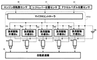
- the automatic transmission control ATCU includes load driving semiconductors 44a, 44b,..., 44e including a load driving circuit 34 and a microcontroller 43 for controlling the load driving semiconductors 44a, 44b,.
- the microcontroller 43 receives signals from sensors including the engine speed sensor 40, the shift lever position sensor 41, the accelerator pedal position sensor 42, etc., and calculates an optimum gear ratio.
- the solenoids 38a, 38b,..., 38e are current-controlled by load drive semiconductors 44a, 44b,..., 44e in order to hydraulically control the clutch in the transmission. This control current flows from the battery VB to the load drive semiconductors 44a, 44b,..., 44e via the solenoids 38a, 38b,.
- the maximum current of the solenoid 38 at which the low-side transistors 30 and 31 are thermally destroyed can be increased in the load dump state.
- the present invention is not limited to the above-described embodiment, and includes various modifications.
- the above-described embodiment has been described in detail for easy understanding of the present invention, and is not necessarily limited to the one having all the configurations described.
- a part of the configuration of an embodiment can be replaced with the configuration of another embodiment, and the configuration of another embodiment can be added to the configuration of an embodiment.
- a MOSFET in which a semiconductor substrate and a plurality of transistors provided on the semiconductor substrate are arranged in parallel, and the MOSFET is composed of a first group of transistors and a second group of transistors.
- the source of the first group of transistors is electrically connected to the source of the second group of transistors;
- the drain of the first group of transistors is electrically connected to the drain of the second group of transistors;
- An active clamp circuit that turns on the MOSFET when the drain voltage exceeds a predetermined voltage is connected between the gate and drain of the first group of transistors, and the gate of the second group of transistors and the active
- An active clamp cutoff circuit is connected between the clamp circuit and the semiconductor device
- the MOSFET When the drain voltage of the MOSFET becomes equal to or higher than the clamp voltage, current flows in the active clamp circuit, current flows in the gate resistance of the MOSFET, and the gate voltage increases, so that the MOSFET is in a driving state. It becomes a state.
- the temperature of the second group of transistors in the active clamp state is higher than the temperature of the first group of transistors.
- the active clamp cutoff circuit operates.
- the gates of the second group of transistors and the active clamp circuit are electrically disconnected, and only the second group of transistors is brought into a non-conductive state.
- An IGBT in which a semiconductor substrate and a plurality of transistors provided on the semiconductor substrate are arranged in parallel, and the IGBT is composed of a first group of transistors and a second group of transistors.
- the emitter of the first group of transistors is electrically connected to the emitter of the second group of transistors, and the collector of the first group of transistors is electrically connected to the collector of the second group of transistors;
- An active clamp circuit that turns on the IGBT when the collector voltage exceeds a predetermined voltage is connected between the gate and collector of the first group of transistors, and the gate of the second group of transistors and the active
- An active clamp cutoff circuit is connected between the clamp circuit and the semiconductor device.
- the collector voltage of the IGBT becomes equal to or higher than the clamp voltage
- a current flows through the active clamp circuit
- a current flows through the gate resistance of the IGBT, and the gate voltage increases, so that the IGBT is driven. It becomes a state.
- the temperature of the second group of transistors is higher than the temperature of the first group of transistors.
- the active clamp cutoff circuit operates.
- the gates of the second group of transistors and the active clamp circuit are electrically disconnected, and only the second group of transistors is brought into a non-conductive state.
- the current energy generated at the output terminal can be absorbed by continuing to drive the transistors other than the center while suppressing the increase in the temperature of the transistor in the center where the temperature is highest during active crunching. it can. For this reason, since the uniformity of the temperature of the transistor can be increased, the thermal breakdown energy of the transistor can be improved. In addition, the amount of increase in the junction temperature at the center of the transistor during active clamp operation is suppressed, and the temperature setting for detecting overtemperature is brought close to the maximum guaranteed operating temperature, so that the transistor can be operated at a higher temperature. Make it possible.
- a temperature detection circuit that detects the junction temperature of the MOSFET or IGBT is connected to the active clamp cutoff circuit, and when the junction temperature of the MOSFET or IGBT detected by the temperature detection circuit exceeds a predetermined threshold value,
- the semiconductor device according to any one of (3) to (4), wherein the active clamp cutoff circuit operates to electrically disconnect the active clamp circuit and the gates of the second group of transistors.
- a temperature detection circuit for detecting the junction temperature of the MOSFET or IGBT is connected to the active clamp cutoff circuit, and when the junction temperature of the MOSFET or IGBT detected by the temperature detection circuit exceeds a predetermined threshold value, The active clamp cutoff circuit operates, and the active clamp circuit and the gates of the second group of transistors are electrically connected via a resistance element.
- Semiconductor device Semiconductor device.
- the temperature detection circuit includes a thermal diode disposed in or near the transistor, and includes a comparison circuit that compares a voltage generated by the thermal diode with a reference voltage.
- the semiconductor device according to any one of (5) to (6).
- the active clamp cutoff circuit operates and the PMOS transistor becomes non-conductive.
- the active clamp circuit and the gates of the second group of transistors are electrically connected via the resistance element.
- the second group of transistors becomes non-conductive, and an increase in the temperature of the second group of transistors having a temperature higher than that of the first group of transistors can be suppressed.
- the uniformity of the temperature of the transistor can be increased, the allowable energy for not exceeding the thermal breakdown energy of the transistor or the rated temperature of the transistor can be increased.
- the amount of increase in the junction temperature at the center of the transistor during active clamp operation is suppressed, and the temperature setting for detecting overtemperature is brought close to the maximum guaranteed operating temperature, so that the transistor can be operated at a higher temperature. Make it possible.
- the active clamp cutoff circuit operates and the PMOS transistor becomes non-conductive.
- the second group of transistors becomes non-conductive, and an increase in the temperature of the second group of transistors having a temperature higher than that of the first group of transistors can be suppressed.
- the uniformity of the temperature of the transistor can be increased, the allowable energy for not exceeding the thermal breakdown energy of the transistor or the rated temperature of the transistor can be increased.
- the amount of increase in the junction temperature at the center of the transistor during active clamp operation is suppressed, and the temperature setting for detecting overtemperature is brought close to the maximum guaranteed operating temperature, so that the transistor can be operated at a higher temperature. Make it possible.
- the active clamp cutoff circuit includes a PMOS transistor and a resistance element connected in parallel with the PMOS transistor.
- the active clamp cutoff circuit operates and the PMOS transistor becomes non-conductive.
- the active clamp circuit and the gates of the second group of transistors are electrically connected via the resistance element.
- the gate voltage of the second group of transistors is lower than the gate voltage of the first group of transistors, and the current density of the second group of transistors is suppressed to a low level.
- An increase in temperature of the two groups of transistors can be suppressed. For this reason, since the uniformity of the temperature of the transistor can be increased, the allowable energy for not exceeding the thermal breakdown energy of the transistor or the rated temperature of the transistor is increased.
- the amount of increase in the junction temperature at the center of the transistor during active clamp operation is suppressed, and the temperature setting for detecting overtemperature is brought close to the maximum guaranteed operating temperature, so that the transistor can be operated at a higher temperature. Make it possible.
- active clamp detection circuit active clamp detection circuit 27: Comparator 28 ... Determination voltage source (reference power supply) 29... Power transistor 30... Low side power transistor (low side transistor) composed of a non-central MOSFET 31 ... Low-side power transistor (low-side transistor) composed of MOSFET in the center 32 ... High-side power transistor (High-side transistor) 33 ... Gate resistance 34 ... Load drive circuit 35 ... Power supply terminal 36 ... Low side input terminal 37 ... High side input terminal 38 ... Solenoid 39 ... Automatic transmission 40 ... Engine speed sensor 41 ... Shift lever position sensor 42 ... Accelerator pedal position sensor 43 ... Microcontroller 44 ... Load drive semiconductors P1, P2 ... Connection points R1, R2 ... Path
Landscapes
- Semiconductor Integrated Circuits (AREA)
- Electronic Switches (AREA)
Abstract
電流性能を維持しつつ、アクティブクランプ状態におけるトランジスタの温度の均一性を向上することができる半導体装置を提供する。 パワートランジスタ14は、パワートランジスタ13に並列接続される。アクティブクランプ回路8は、パワートランジスタ13とパワートランジスタ14との間の接続点P1からパワートランジスタ13のゲートまでの経路R1に設けられ、接続点P1の電圧が第1閾値を超えた場合、導通する。アクティブクランプ遮断回路12は、アクティブクランプ回路12からパワートランジスタ14のゲートまでの経路R2に設けられ、経路R2に流れる電流を遮断又は抑制する。
Description
本発明は、半導体装置に関する。
車載ECU(Electrical Control Unit)に搭載されるソレノイド負荷などの駆動回路を構成する半導体装置には、30V以上の高耐圧とアンペアオーダーの高い電流駆動能力に加え、誤動作やパワートランジスタの素子破壊が生じないように出力端子に発生した電流エネルギーを吸収することが求められる。このため、出力段のパワートランジスタのゲートとドレインにアクティブクランプ回路を設ける方法がある(例えば、特許文献1参照)。これによって、出力端子に発生した電流エネルギーをグランドに放出することができる。
ここで、アクティブクランプ動作時におけるパワートランジスタで消費可能な電流エネルギー(熱破壊エネルギー)はトランジスタの自己発熱による熱暴走の発生条件によって決まり、一般にトランジスタサイズを大きくすることで、その値を大きくすることができる。しかしながら、トランジスタサイズの増大はチップコストの増大を招く問題がある。
一方、サイズの比較的大きなパワートランジスタにおいては、その放熱性が異なるために、その中央領域と周辺領域で温度差が生じる。すなわち、放熱性が悪い中央領域ではより温度が高くなっているが、周辺領域では放熱効果によって温度が低くなっている。この結果、トランジスタの熱破壊エネルギーをサイズ増大相当分大きくすることができないという問題や、信頼性の観点からトランジスタの接合温度が、定格温度を超えないようにするため、許容エネルギー量が小さく制限される他、トランジスタの使用環境温度を高くすることができないといった問題がある。
この問題に対して、トランジスタ内の温度分布を一様にするための技術が開示されている。その1つは、並列に配置されたトランジスタの能動領域の間隔を中央領域で大きくし、周辺領域で小さくする方法で(例えば、特許文献2参照)、もう1つは中央領域の入力電力を周辺領域の入力電力より低減する方法である。いずれの方法も、単位面積あたりの消費電力を周辺領域から中央領域に向けて減少させることにより、トランジスタ内の温度分布を一様にすることができ、その結果、トランジスタの熱破壊エネルギーを高めることができる。
また、パワートランジスタの中央領域に非活性領域を設け、非活性領域上に放熱用電極を形成する技術が開示されている(例えば、特許文献3参照)。温度が高くなる中央領域を非活性化することで、トランジスタ内の温度を低減できると共に温度の均一性を向上できる。また、放熱用電極を介して半導体外部に放熱することで、温度をさらに低減することができる。この結果、トランジスタの熱破壊エネルギーを高めることができる。
また、パワートランジスタの温度が所定温度以上かどうかを検出する過温度検出回路を持った半導体集積回路で、トランジスタの温度が所定以上となったときに、トランジスタを非駆動とすると共に、第1のクランプ電圧より低い第2のクランプ電圧で、パワートランジスタをアクティブクランプ状態にする技術が開示されている(例えば、特許文献4参照)。サージエネルギーを消費する時間を長くして、トンジスタの急激な温度上昇を抑えることができるため、過温度と検知するための温度設定を最大の動作保証温度に近づけることができる。この結果、より高温でトランジスタを動作させることが可能になる。
しかしながら、特許文献2に開示されるような技術では、いずれもトランジスタの消費電力密度を周辺領域から中央領域に向けて小さくなるように、中央領域のトランジスタと周辺領域のトランジスタとで能動領域の間隔や形状を変えている。このため、通常動作時にトランジスタの面積あたりの性能が中央領域で低下するという問題がある。また、トランジスタ形状を変える必要があるためにトランジスタの構造設計が複雑になるといった問題がある。
また、特許文献3に開示されるような方法では、トランジスタの温度の均一性は向上できるものの、通常動作時のトランジスタの電流性能を同一とするには、非活性領域を設けない場合と比べて、非活性領域分だけトランジスタのサイズが大きくなるという問題がある。
また、特許文献4に開示されるような方法では、通常動作時のトランジスタの面積あたりの電流性能を低下させること無く、過温度検出時のクランプ電圧を下げることにより、急激な温度上昇を抑えられ、熱破壊エネルギーを増大することができる。一方、アクティブクランプ状態における、トランジスタの接合温度は中央部が周辺部に比べて高くなる問題は残っており、トランジスタ中央部の接合温度が最大定格温度を超えないように電流エネルギー量が制限されるという問題がある。また、電流エネルギーを消費する時間が長くなるために、アクティブクランプ動作の時間が増大するという問題がある。
本発明の目的は、電流性能を維持しつつ、アクティブクランプ状態におけるトランジスタの温度の均一性を向上することができる半導体装置を提供することにある。
上記目的を達成するために、本発明は、第1制御電極を有する第1トランジスタと、前記第1トランジスタに並列接続され、第2制御電極を有する第2トランジスタと、前記第1トランジスタと前記第2トランジスタとの間の第1接続点から前記第1制御電極までの第1経路に設けられ、前記第1接続点の電圧が第1閾値を超えた場合、導通するアクティブクランプ回路と、前記アクティブクランプ回路から前記第2制御電極までの第2経路に設けられ、前記第2経路に流れる電流を遮断又は抑制するアクティブクランプ遮断回路と、を備える。
本発明によれば、電流性能を維持しつつ、アクティブクランプ状態におけるトランジスタの温度の均一性を向上することができる。上記した以外の課題、構成及び効果は、以下の実施形態の説明により明らかにされる。
以下、図面を用いて、本発明の第1~第4の実施形態による負荷駆動回路(半導体装置)の構成及び動作について説明する。なお、各図において、同一符号は同一部分を示す。本発明の実施形態による負荷駆動回路は、前述した目的と一部重複するが、例えば、次の第1~第2の目的を達成しようとするものである。
第1の目的は、トランジスタサイズを増大させることなく、また、通常動作時におけるトランジスタの面積あたりの電流性能を低下させることなく、アクティブクランプ時のトランジスタの温度の均一性を向上させて、トランジスタの熱破壊エネルギーやトランジスタが定格温度を越えないための許容エネルギーを増大することにある。
また、第2の目的は、アクティブクランプ時間を増大すること無く、アクティブクランプ動作時のトランジスタの温度の均一性を向上させることで、より高温の環境下でトランジスタを動作させることを可能とすることにある。
(比較例)
最初に、図10を用いて、本発明の実施形態との比較例であるアクティブクランプ回路8を持った負荷駆動回路6Pの構成及び基本動作を簡単に説明する。
最初に、図10を用いて、本発明の実施形態との比較例であるアクティブクランプ回路8を持った負荷駆動回路6Pの構成及び基本動作を簡単に説明する。
電磁負荷2(誘導負荷)からの大きな誘導性電流エネルギーの放出や電流ノイズによって、絶対最大定格を超えるような電圧が出力端子4に発生したときに、ツェナーダイオード15、16がアバランシェ降伏して、アクティブクランプ回路8に電流が流れ、パワートランジスタ29のソース・ゲート間に接続されたゲート抵抗9に電流が流れて、パワートランジスタ29をオン(アクティブクランプ動作)させる。これによって、出力端子4に発生した電流エネルギーをグランドに放出することができる。
(第1の実施形態)
図1乃至5は本発明の実施形態を示しており、以下これについて説明する。
図1乃至5は本発明の実施形態を示しており、以下これについて説明する。
図1は第1の実施形態による負荷駆動回路6(半導体装置)の回路図である。負荷駆動回路6は、半導体基板上に形成された第1群のMOSFET(半導体素子)で構成されるパワートランジスタ13と、第2群のMOSFETで構成されるパワートランジスタ14をもち、前記第1群のMOSFETで構成されるパワートランジスタ13のソースは前記第2群のMOSFETで構成されるパワートランジスタ14のソースと電気的に接続されている。また、前記第1群のMOSFETで構成されるパワートランジスタ13のドレインは前記第2群のMOSFETで構成されるパワートランジスタ14のドレインと電気的に接続されている。
換言すれば、パワートランジスタ14(第2トランジスタ)は、パワートランジスタ13(第1トランジスタ)に並列接続される。
前記第1群のMOSFETで構成されるパワートランジスタ13のゲートとソース間には、ゲート抵抗9が接続され、ゲートとドレイン間には、アクティブクランプ回路8が接続されている。さらに、前記第2群のMOSFETで構成されるパワートランジスタ14のゲートとソース間には、ゲート抵抗10が接続され、ゲートと前記アクティブクランプ回路8間には、アクティブクランプ(ACP)遮断回路12が接続される。
換言すれば、アクティブクランプ回路8は、パワートランジスタ13(第1トランジスタ)とパワートランジスタ14(第2トランジスタ)との間の接続点P1(第1接続点)からパワートランジスタ13のゲート(第1制御電極)までの経路R1(第1経路)に設けられ、接続点P1の電圧が第1閾値を超えた場合、導通する。ゲート抵抗9(第1抵抗)は、パワートランジスタ13とパワートランジスタ14との間の接続点P2(第2接続点)とパワートランジスタ13のゲート(第1制御電極)の間に接続される。また、ゲート抵抗10(第2抵抗)は、接続点P2とパワートランジスタ14のゲート(第2制御電極)の間に接続される。アクティブクランプ遮断回路12は、アクティブクランプ回路12からパワートランジスタ14のゲート(第2制御電極)までの経路R2(第2経路)に設けられ、経路R2に流れる電流を遮断又は抑制する。
前記アクティブクランプ回路8は、直列に接続された逆流防止ダイオード17とツェナーダイオード15、16からなる。また、アクティブクランプ遮断回路12には、前記パワートランジスタ13、14の温度を検出する温度検出回路11が接続されている。
ここで、アクティブクランプ遮断回路12は図4にその実施例を示すように、PMOSトランジスタ21で構成されており、ソースがアクティブクランプ回路8に、ドレインがパワートランジスタ14のゲートに、ゲートが温度検出回路11に接続されている。温度検出回路11は通常時はLOWを出力し、PMOSトランジスタ21はオン状態となって、アクティブクランプ回路8とパワートランジスタ14のゲート間が電気的に接続されている。
また、温度検出回路11は図5にその実施例を示すように、パワートランジスタ13、14の温度を検出するための感熱ダイオード22は電流源23と、比較器24に接続されている。ダイオードの順方向電圧Vfは温度増大と共に低下して、所定の判定電圧Vref(基準電圧)以下となると比較器24の出力はLOWからHighとなるように構成されている。なお、感熱ダイオード22は、熱応答性を良くするために、パワートランジスタ14の内部、もしくは近傍に配置されることが望ましい。
換言すれば、温度検出回路11は、パワートランジスタ14(第2トランジスタ)の温度を検出する。アクティブクランプ遮断回路12は、パワートランジスタ14の温度が第2閾値以下である場合にオンし、パワートランジスタ14の温度が第2閾値を超える場合にオフするPMOSトランジスタ21(第3トランジスタ)を有する。
次に、図2に前記第1群のMOSFETで構成されるパワートランジスタ13と前記第2群のMOSFETで構成されるパワートランジスタ14の平面構造を示す。パワートランジスタは複数のMOSFETからなり、第2群のMOSFETは中央部に位置するMOSFETで構成され、第1群のMOSFETは非中央部のMOSFETで構成されている。
換言すれば、パワートランジスタ13(第1トランジスタ)は、半導体基板上の第1領域(図2に示す太い破線で囲まれる領域)に形成される。パワートランジスタ14(第2トランジスタ)は、第1領域に隣接する第2領域(図2に示す細い破線で囲まれる領域)に形成される。詳細には、第1領域は、第2領域に隣接する2つの領域から構成される。第2領域は、半導体基板の中央部に位置する。なお、パワートランジスタ14がオンの場合のパワートランジスタ14の温度は、パワートランジスタ13がオンの場合のパワートランジスタ13の温度よりも高い。
図には記載されていないが、各ソース19は互いに配線層(ソース用)により電気的に接続され、各ドレイン20は互いに配線層(ドレイン用)により電気的に接続される。第1群のMOSFETのゲート18は配線層Gate1により互いに接続されて、第2群のMOSFETのゲート18は配線層Gate2により互いに接続されている。
続いて、図1に示す負荷駆動回路6の動作を説明する。アクティブクランプ状態にない通常動作時において、アクティブクランプ遮断回路12は導通状態にあり、第1群のMOSFETで構成されるパワートランジスタ13のゲート(配線層Gate1)と第2群のMOSFETで構成されるパワートランジスタ14のゲート(配線層Gate2)は電気的に接続されるように構成され、入力端子3に入力された制御信号は、バッファ7を介して、配線層Gate1及びGate2に供給され、パワートランジスタ13、14のゲートは同じ電圧で駆動される。このため、第1群のMOSFETで構成されるパワートランジスタ13と第2群のMOSFETで構成されるパワートランジスタ14の面積あたりの電流性能は等しくなり、図10に示す比較例におけるパワートランジスタ29と同等の面積あたりの電流性能を示す。
次に、電流ノイズや電磁負荷からの電流エネルギー放出によって、出力端子4の電圧が所定の電圧以上となった場合、アクティブクランプ回路8にはツェナーダイオード15、16がブレークダウンすることで電流が流れる。この電流が、第1群のMOSFETで構成されるパワートランジスタ13のゲートに接続されるゲート抵抗9に流れることで、ゲートの電圧が上昇して、パワートランジスタ13は駆動状態となる。この状態をアクティブクランプ状態といい、トランジスタのドレイン電圧は所望の電圧(クランピング電圧)にクランプされる。
一方、アクティブクランプ回路8からの電流は、第2群のMOSFETで構成されるパワートランジスタ14のゲートに接続されるゲート抵抗10にも流れるために、ゲート電圧が上昇して、パワートランジスタ14は駆動状態となり、同様にアクティブクランプ状態となる。
この時、パワートランジスタ13、14ではドレイン電流とクランプ電圧の積で与えられる比較的大きな電力が消費されるために、自己発熱によってその接合温度が時間と共に増大する。図11は比較例におけるアクティブクランプ時のトランジスタ内の温度の時間的変化を示す。トランジスタ内の温度分布は、電力密度が一定となる条件下では、放熱効果の差によって、トランジスタの中央部が最も温度が高くなり、周辺部で小さくなる(TC1>Tp1)。一方、トランジスタの温度は、定格温度Tjmaxを超えないようにする必要があるために、Tjmax>TC1となるように、アクティブクランプ時のエネルギー量と使用環境温度Taが制限される。
図3は本発明の第1の実施形態における、アクティブクランプ時のトランジスタ内の温度の時間的変化を示す。アクティブクランプ動作が開始(t0)した直後の温度変化は、比較例(図11参照)と変わらないが、温度検出回路11にて、中央部のMOSFETで構成されるパワートランジスタ14の温度が所定の温度を超えることを検出すると、アクティブクランプ遮断回路12が動作して、中央部のMOSFETで構成されるアクティブクランプ回路8とパワートランジスタ14のゲートが電気的に非接続状態となり、パワートランジスタ14は非駆動状態となる。
一方、非中央部のMOSFETで構成されるパワートランジスタ13はアクティブクランプ状態が継続される。この結果、中央部のパワートランジスタ14のみ発熱が抑えられて、トランジスタ中央部の温度は低下もしくは温度上昇が抑制されるが、非中央部のパワートランジスタ13は発熱し続けるために、非中央部のトランジスタの温度は増大し続ける。
この結果、トランジスタ中央部の温度(Tc3)と周辺部の温度(Tp3)差が小さくなって、トランジスタの温度の均一性が上がると共に、アクティブクランプ時のトランジスタの最大温度が比較例(図11参照)に比べて低減できる(TC2<TC1、TC3<TC1)。このため、使用環境温度Taを増大できる。また、同じ使用環境温度Ta条件では、アクティブクランプ時により多くのエネルギーをパワートランジスタが消費することが可能となる。さらにこの効果によって、電流エネルギーに対する、パワートランジスタの熱破壊耐性を向上でき、熱破壊エネルギーを向上することができる。
なお、本実施例では、パワートランジスタ13、14をMOSトランジスタとしたが、IGBT(半導体素子)とすることもでき、その際のトランジスタ動作は、MOSトランジスタと同様である。
また、本実施例では、パワートランジスタ13を非中央部の第1群のMOSFETで構成し、パワートランジスタ14を中央部の第2群のMOSFETで構成しているが、この限りではなく、パワートランジスタ14を構成する第2群のMOSFETを中央部に重み付けをした複数の領域に分けて構成(配置)するなどとしても、アクティブクランプ時のパワートランジスタの温度の均一性を上げることが可能である。
以上説明したように、本実施形態によれば、電流性能を維持しつつ、アクティブクランプ状態におけるトランジスタの温度の均一性を向上することができる。
詳細には、トランジススタサイズを大きくすることなく、また、通常動作時におけるトランジスタの面積あたりの電流性能の低下をさせることなく、アクティブクランプ動作時のトランジスタ中央部の温度の増大量を抑えると共に、トランジスタ内の接合温度の均一性を上げることで、トランジスタの熱破壊エネルギーやトランジスタの定格温度を越えない中での許容エネルギーを増大することができる。
また、アクティブクランプ時間を増大すること無く、アクティブクランプ動作時のトランジスタの中央部の接合温度の増大量を抑えて、過温度と検知するための温度設定を最大の動作保証温度に近づけることで、より高温でトランジスタを動作させることができる。
(第2の実施形態)
図6は本発明の第2の実施形態による回路図を示す。第1の実施形態との差分は、アクティブクランプ遮断回路12が、PMOSトランジスタ21とPMOSトランジスタ21に並列に接続された、ゲート電圧低減抵抗26(抵抗)を備えている点にある。非アクティブクランプ状態である通常動作時は、PMOSトランジスタ21がオン状態にあって、アクティブクランプ回路8とパワートランジスタ14のゲートは低インピーダンスで接続されるので、第1の実施形態と同様な動作状態となる。
図6は本発明の第2の実施形態による回路図を示す。第1の実施形態との差分は、アクティブクランプ遮断回路12が、PMOSトランジスタ21とPMOSトランジスタ21に並列に接続された、ゲート電圧低減抵抗26(抵抗)を備えている点にある。非アクティブクランプ状態である通常動作時は、PMOSトランジスタ21がオン状態にあって、アクティブクランプ回路8とパワートランジスタ14のゲートは低インピーダンスで接続されるので、第1の実施形態と同様な動作状態となる。
一方、アクティブクランプ状態にあって、温度検出回路11がHigh出力となり、PMOSトランジスタ21がオフ状態となった場合、アクティブクランプ回路8とパワートランジスタ14のゲート(配線層Gate2)とはゲート電圧低減抵抗26を介して接続される。
この結果、パワートランジスタ14のゲート電圧はゲート電圧低減抵抗26とゲート抵抗10の分圧比で決まる電圧となって、PMOSトランジスタがオン状態にある時と比べて、ゲート電圧は小さくなる。これにより、中央部にあるパワートランジスタ14のドレイン電流が小さくなって、面積あたりの消費電力は、非中央部にあるパワートランジスタ13に比べて小さくなる。この結果、パワートランジスタ13、14の温度の均一性を向上でき、第1の実施形態と同様な効果を得ることができるが、ゲート電圧低減抵抗26の抵抗値を調整することで、中央部のパワートランジスタ14のアクティブクランプ時のドレイン電流を自由に調整できるため、第1の実施形態に比べて、アクティブクランプ時のトランジスタの温度の均一性をより向上することができる。
(第3の実施形態)
図7は本発明の第3の実施形態による回路図を示す。第2の実施形態との差分は、温度検出回路11(図6)が、アクティブクランプ検出回路26A(図7)となっている点である。非アクティブクランプ状態である通常動作時は、PMOSトランジスタ21がオン状態にあって、アクティブクランプ回路8とパワートランジスタ14のゲートは低インピーダンスで接続されるので、第1の実施形態と同様な動作状態となる。
図7は本発明の第3の実施形態による回路図を示す。第2の実施形態との差分は、温度検出回路11(図6)が、アクティブクランプ検出回路26A(図7)となっている点である。非アクティブクランプ状態である通常動作時は、PMOSトランジスタ21がオン状態にあって、アクティブクランプ回路8とパワートランジスタ14のゲートは低インピーダンスで接続されるので、第1の実施形態と同様な動作状態となる。
アクティブクランプ検出回路26Aは、出力端子4の電圧と判定電圧源28を入力とする比較器からなり、出力端子4の電圧が判定電圧Vref2より大きくなると、アクティブクランプ検出回路26Aの出力がHigh状態となって、アクティブクランプ遮断回路12のPMOSトランジスタ21がオフ状態になる。
換言すれば、アクティブクランプ検出回路26Aは、アクティブクランプ回路8が導通している状態を示すアクティブクランプ状態を検出する。アクティブクランプ遮断回路12は、アクティブクランプ状態が検出されない場合にオンし、アクティブクランプ状態が検出された場合にオフするPMOSトランジスタ21(第3トランジスタ)を有する。
この結果、アクティブクランプ回路8と中央部のパワートランジスタ14のゲートはゲート電圧低減抵抗26を介して接続されて、第2の実施形態と同様に、抵抗分圧されたゲート電圧がパワートランジスタ14に印加される。このため、中央部にあるパワートランジスタ14のドレイン電流が小さくなって、面積あたりの消費電力は、非中央部にあるパワートランジスタ13に比べて小さくなる。この結果、パワートランジスタ13、14の温度の均一性を向上でき、第2の実施形態と同様な効果を得ることができるが、温度検出回路を用いた第2の実施形態に比べて、アクティブクランプ動作開始直後から、中央部のパワートランジスタ14の面積あたりの消費電力が、非中央部のパワートランジスタ13の面積あたりの消費電力に比べて小さくなっており、アクティブクランプ時のパワートランジスタ13、14の温度の均一性をより向上することができる。
なお、アクティブクランプ検出回路26Aにおける、比較器27の入力はかならずしも出力端子4とする必要は無く、ツェナーダイオード15あるいはツェナーダイオード16のカソード電圧とすることもできる。さらに、アクティブクランプ回路8に抵抗素子(センス抵抗等)を接続して、所望の電流がアクティブクランプ回路8に流れた時に、抵抗素子の電圧降下を検出することで構成することもできる。
(第4の実施形態)
第1の実施形態による負荷駆動回路をローサイドに用いて、ハイサイドトランジスタ32とローサイドトランジスタ30、31で構成されるソレノイド38を駆動する負荷駆動回路34を構成したものを図8に示す。ローサイド入力端子36とハイサイド入力端子37を通じてPWM制御信号が入力され、通常動作においては、ソレノイド38を駆動する電流が出力端子4を通じて流れる。電流量を増大する時はローサイドトランジスタ30、31がオン状態に、電流量を減少する時はハイサイドトランジスタ32がオン状態になるが、両トランジスタが同時にオン状態とならないように、両トランジスタがいずれもオフ状態となる期間がある。この時、ソレノイド38に流れる電流は出力端子4からハイサイドトランジスタ32と並列に接続されるダイオードを通じて電源端子35を経て、ソレノイド38に流れ込む環流状態となる。
第1の実施形態による負荷駆動回路をローサイドに用いて、ハイサイドトランジスタ32とローサイドトランジスタ30、31で構成されるソレノイド38を駆動する負荷駆動回路34を構成したものを図8に示す。ローサイド入力端子36とハイサイド入力端子37を通じてPWM制御信号が入力され、通常動作においては、ソレノイド38を駆動する電流が出力端子4を通じて流れる。電流量を増大する時はローサイドトランジスタ30、31がオン状態に、電流量を減少する時はハイサイドトランジスタ32がオン状態になるが、両トランジスタが同時にオン状態とならないように、両トランジスタがいずれもオフ状態となる期間がある。この時、ソレノイド38に流れる電流は出力端子4からハイサイドトランジスタ32と並列に接続されるダイオードを通じて電源端子35を経て、ソレノイド38に流れ込む環流状態となる。
ここで、この環流状態において、何らかの原因で、電源端子35と電源1とがオープン状態なる異常(ロードダンプ状態)が発生した場合、ソレノイド38に流れる電流は行き場を失うことになるため、出力端子4の電圧は増大し、電源電圧VBを越える。出力端子4の電圧がツェナーダイオード15、16のブレークダウン電圧以上となると出力端子4からツェナーダイオード15、16に電流が流れて、ローサイドトランジスタ30、31のゲート抵抗9、10に電流が流れる。これにより出力端子4の電圧が、ローサイドトランジスタ30、31のソース・ドレイン間の耐圧電圧となる前に、ローサイドトランジスタ30、31がオンして、ソレノイド38からの電流を流すことができる。
この時、ローサイドトランジスタ30、31は高い電力消費のため発熱するが、トランジスタの中央部は特に温度が増大する。温度検出回路11でこの温度を検出し、一定の閾値を超えた場合、熱によるトランジスタの破壊を防ぐために、中央領域にあるローサイドトランジスタ31のみをアクティブクランプ遮断回路12により、オフ状態にする。一方、非中央領域にあるローサイドトランジスタ30はオン状態を維持して、ソレノイド38からの電流を流す。これにより、ローサイドトランジスタ30、31が熱破壊するソレノイド38の最大電流を増大することができる。
図9はこの負荷駆動回路34を自動変速機制御ATCU(Automatic Transmission Control Unit)に用いた場合の装置構成図を示す。自動変速制御ATCUは、負荷駆動回路34を含む負荷駆動半導体44a、44b、…、44eとこれを制御するマイクロコントローラ43からなる。マイクロコントローラ43は、エンジン回転数センサ40、シフトレバー位置センサ41、アクセルペダル位置センサ42などからなるセンサからの信号を入力として、最適な変速比を算出する。ソレノイド38a、38b、 …、38eは変速機内のクラッチを油圧で制御するために、負荷駆動半導体44a、44b、…、44eにより電流制御される。なお、この制御電流はバッテリーVBからソレノイド38a、38b、 …、38eを経て負荷駆動半導体44a、44b、…、44eに流れる。
以上説明したように、本実施形態による自動変速機制御ATCUによれば、ロードダンプ状態において、ローサイドトランジスタ30、31が熱破壊するソレノイド38の最大電流を増大することができる。
なお、本発明は上記した実施形態に限定されるものではなく、様々な変形例が含まれる。例えば、上述した実施形態は本発明を分かりやすく説明するために詳細に説明したものであり、必ずしも説明した全ての構成を備えるものに限定されるものではない。また、ある実施形態の構成の一部を他の実施形態の構成に置き換えることが可能であり、また、ある実施形態の構成に他の実施形態の構成を加えることも可能である。また、各実施形態の構成の一部について、他の構成の追加・削除・置換をすることが可能である。
なお、本発明の実施形態は、以下の態様であってもよい。
(1)半導体基板と、前記半導体基板上に設けられた複数のトランジスタが並列に配置されたMOSFETであって、前記MOSFETは、第1群のトランジスタと、第2群のトランジスタで構成されていて、第1群のトランジスタのソースは第2群のトランジスタのソースと電気的に接続されていて、第1群のトランジスタのドレインは第2群のトランジスタのドレインと電気的に接続されていて、前記ドレイン電圧が所定の電圧を超えると前記MOSFETをオン状態とするアクティブクランプ回路が前記第1群のトランジスタのゲートとドレインとの間に接続されていて、前記第2群のトランジスタのゲートと前記アクティブクランプ回路との間には、アクティブクランプ遮断回路が接続されていていることを特徴とする半導体装置。
前記MOSFETのドレイン電圧がクランプ電圧以上となった時に、アクティブクランプ回路に電流が流れて、前記MOSFETのゲート抵抗に電流が流れ、ゲート電圧が増大することで、前記MOSFETが駆動状態となるアクティブクランプ状態となる。アクティブクランプ状態における、第2群のトランジスタの温度は、第1群のトランジスタの温度に比べて高くなっているが、前記MOSFETの温度が所定の温度以上となると、前記アクティブクランプ遮断回路が動作して、第2群のトランジスタのゲートとアクティブクランプ回路が電気的に非接続として、第2群のトランジスタのみ非導通状態とする。
かかる構成により、第1群のトランジスタと比べて温度が高い第2群のトランジスタの温度の上昇を抑えながら、第1群のトランジスタの駆動を継続して電流エネルギーを吸収することができる。このため、トランジスタの温度の均一性を上げられるため、トランジスタの熱破壊エネルギーを向上することができる。また、非アクィテブクランプ状態の通常動作時には、第1群のトランジスタと第2群のトランジスタのゲートは電気的に接続されるため、トランジスタの面積あたりの電流性能を低下させることなく、トランジスタの熱破壊エネルギーやトランジスタの定格温度を越えないための許容エネルギーを増大することができる。また、クランプ電圧の電圧は一定であるために、アクティブクランプ時間が増大することもない。
(2)半導体基板と、前記半導体基板上に設けられた複数のトランジスタが並列に配置されたIGBTであって、前記IGBTは、第1群のトランジスタと、第2群のトランジスタで構成されていて、第1群のトランジスタのエミッタは第2群のトランジスタのエミッタと電気的に接続されていて、第1群のトランジスタのコレクタは第2群のトランジスタのコレクタと電気的に接続されていて、前記コレクタ電圧が所定の電圧を超えると前記IGBTをオン状態とするアクティブクランプ回路が前記第1群のトランジスタのゲートとコレクタとの間に接続されていて、前記第2群のトランジスタのゲートと前記アクティブクランプ回路との間には、アクティブクランプ遮断回路が接続されていていることを特徴とする半導体装置。
前記IGBTのコレクタ電圧がクランプ電圧以上となった時に、アクティブクランプ回路に電流が流れて、前記IGBTのゲート抵抗に電流が流れ、ゲート電圧が増大することで、前記IGBTが駆動状態となるアクティブクランプ状態となる。アクティブクランプ状態における、第2群のトランジスタの温度は、第1群のトランジスタの温度に比べて高くなっているが、前記IGBTの温度が所定の温度以上となると、前記アクティブクランプ遮断回路が動作して、第2群のトランジスタのゲートとアクティブクランプ回路が電気的に非接続として、第2群のトランジスタのみ非導通状態とする。
かかる構成により、第1群のトランジスタと比べて温度が高い第2群のトランジスタの温度の上昇を抑えながら、第1群のトランジスタの駆動を継続して電流エネルギーを吸収することができる。このため、トランジスタの温度の均一性を上げられるため、トランジスタの熱破壊エネルギーを向上することができる。また、非アクィテブクランプ状態の通常動作時には、第1群のトランジスタと第2群のトランジスタのゲートは電気的に接続されるため、トランジスタの面積あたりの電流性能を低下させることなく、トランジスタの熱破壊エネルギーやトランジスタの定格温度を越えないための許容エネルギーを増大することができる。また、クランプ電圧の電圧は一定であるために、アクティブクランプ時間が増大することもない。
(3)トランジスタ導通時の前記第2群のトランジスタの温度は、トランジスタ導通時の前記第1群のトランジスタの温度より高いことを特徴とする(1)、(2)に記載の半導体装置。
(4)前記第2群のトランジスタは、前記MOSFETもしくはIGBTの中央部にあるトランジスタを含んでいることを特徴とする(3)に記載の半導体装置。
かかる構成により、アクティブクランブ時に最も温度が高くなる中央部にあるトランジスタの温度の増大を抑えながら、中央部以外にあるトランジスタの駆動を継続して出力端子に発生した電流エネルギーを吸収することができる。このため、トランジスタの温度の均一性を上げられるため、トランジスタの熱破壊エネルギーを向上することができる。また、アクティブクランプ動作時のトランジスタの中央部の接合温度の増大量を抑えて、過温度と検知するための温度設定を最大の動作保証温度に近づけることで、より高温でトランジスタを動作させることを可能とする。
(5)前記アクティブクランプ遮断回路には、前記MOSFETもしくはIGBTの接合温度を検出する温度検出回路が接続されて、前記温度検出回路によって検出したMOSFETもしくはIGBTの接合温度が所定の閾値を超えると、記アクティブクランプ遮断回路が動作して、前記アクティブクランプ回路と前記第2群のトランジスタのゲートが電気的に切断されることを特徴とする(3)乃至(4)に記載の半導体装置。
(6)前記アクティブクランプ遮断回路には、前記MOSFETもしくはIGBTの接合温度を検出する温度検出回路が接続されて、前記温度検出回路によって検出したMOSFETもしくはIGBTの接合温度が所定の閾値を超えると、前記アクティブクランプ遮断回路が動作して、前記アクティブクランプ回路と前記第2群のトランジスタのゲートは抵抗素子を介して電気的に接続されることを特徴とする(3)乃至(4)に記載の半導体装置。
(7)前記温度検出回路は、前記トランジスタの内部、もしくは近傍に配置された感熱ダイオードを備えていて、前記感熱ダイオードの生成する電圧と、基準電圧とを比較する比較回路を備えていることを特徴とする(5)乃至(6)に記載の半導体装置。
(8)前記アクティブクランプ遮断回路には、前記MOSFETもしくはIGBTのアクティブクランプ状態を検出するアクティブクランプ検知回路が接続されていることを特徴とする(3)乃至(4)に記載の半導体装置。
かかる構成により、アクティブクランプ状態を検知すると、前記アクティブクランプ遮断回路が動作して、PMOSトランジスタは非導通となる。この結果、前記アクティブクランプ回路と第2群のトランジスタのゲートは前記抵抗素子を介して電気的に接続される。この結果、前記第2群のトランジスタは非導通となり、第1群のトランジスタより温度の高い第2群のトランジスタの温度の増大を抑えることができる。このため、トランジスタの温度の均一性を上げられるため、トランジスタの熱破壊エネルギーやトランジスタの定格温度を越えないための許容エネルギーを増大することができる。また、アクティブクランプ動作時のトランジスタの中央部の接合温度の増大量を抑えて、過温度と検知するための温度設定を最大の動作保証温度に近づけることで、より高温でトランジスタを動作させることを可能とする。
(9)前記アクティブクランプ遮断回路はPMOSトランジスタで構成されることを特徴とする(5)乃至(7)に記載の半導体装置。
かかる構成により、前記トランジスタの温度が所定の温度以上となると前記アクティブクランプ遮断回路が動作して、PMOSトランジスタは非導通となる。この結果、前記第2群のトランジスタは非導通となり、第1群のトランジスタより温度の高い第2群のトランジスタの温度の増大を抑えることができる。このため、トランジスタの温度の均一性を上げられるため、トランジスタの熱破壊エネルギーやトランジスタの定格温度を越えないための許容エネルギーを増大することができる。また、アクティブクランプ動作時のトランジスタの中央部の接合温度の増大量を抑えて、過温度と検知するための温度設定を最大の動作保証温度に近づけることで、より高温でトランジスタを動作させることを可能とする。
(10)前記アクティブクランプ遮断回路はPMOSトランジスタと、前記PMOSトランジスタと並列に接続された抵抗素子で構成されることを特徴とする(6)乃至(7)記載の半導体装置。
かかる構成により、前記トランジスタの温度が所定の温度以上となると前記アクティブクランプ遮断回路が動作して、PMOSトランジスタは非導通となる。この結果、前記アクティブクランプ回路と第2群のトランジスタのゲートは前記抵抗素子を介して電気的に接続される。この結果、第1群のトランジスタのゲート電圧より第2群のトランジスタのゲート電圧は小さくなって、第2群のトランジスタの電流密度が小さく抑えされるので、第1群のトランジスタより温度の高い第2群のトランジスタの温度の増大を抑えることができる。このため、トランジスタの温度の均一性を上げられるため、トランジスタの熱破壊エネルギーやトランジスタの定格温度を越えないための許容エネルギーを増大することにある。また、アクティブクランプ動作時のトランジスタの中央部の接合温度の増大量を抑えて、過温度と検知するための温度設定を最大の動作保証温度に近づけることで、より高温でトランジスタを動作させることを可能とする。
1…電源
2…電磁負荷
3…入力端子
4…出力端子
5…グランド端子
6…負荷駆動回路
7…バッファ
8…アクティブクランプ回路
9、10…ゲート抵抗
11…温度検出回路
12…アクティブクランプ遮断回路
13…非中央部のMOSFETで構成されるパワートランジスタ
14…中央部のMOSFETで構成されるパワートランジスタ
15、16…ツェナーダイオード
17…逆流防止ダイオード
18…ゲート(ゲート電極)
19…ソース(ソース電極)
20…ドレイン(ドレイン電極)
21…PMOSトランジスタ
22…感熱ダイオード
23…電流源
24…比較器
25…温度検出回路出力
26…ゲート電圧低減抵抗
26A…アクティブクランプ検出回路(アクティブクランプ検知回路)
27…比較器
28…判定電圧源(基準電源)
29…パワートランジスタ
30…非中央部のMOSFETで構成されるローサイドパワートランジスタ(ローサイドトランジスタ)
31…中央部のMOSFETで構成されるローサイドパワートランジスタ(ローサイドトランジスタ)
32…ハイサイドパワートランジスタ(ハイサイドトランジスタ)
33…ゲート抵抗
34…負荷駆動回路
35…電源端子
36…ローサイド入力端子
37…ハイサイド入力端子
38…ソレノイド
39…自動変速機
40…エンジン回転数センサ
41…シフトレバー位置センサ
42…アクセルペダル位置センサ
43…マイクロコントローラ
44…負荷駆動半導体
P1、P2…接続点
R1、R2…経路
Claims (11)
- 第1制御電極を有する第1トランジスタと、
前記第1トランジスタに並列接続され、第2制御電極を有する第2トランジスタと、
前記第1トランジスタと前記第2トランジスタとの間の第1接続点から前記第1制御電極までの第1経路に設けられ、前記第1接続点の電圧が第1閾値を超えた場合、導通するアクティブクランプ回路と、
前記アクティブクランプ回路から前記第2制御電極までの第2経路に設けられ、前記第2経路に流れる電流を遮断又は抑制するアクティブクランプ遮断回路と、
を備えることを特徴とする半導体装置。 - 請求項1に記載の半導体装置であって、
半導体基板を備え、
前記第1トランジスタは、
前記半導体基板上の第1領域に形成され、
前記第2トランジスタは、
前記第1領域に隣接する第2領域に形成される
ことを特徴とする半導体装置。 - 請求項2に記載の半導体装置であって、
前記第1領域は、
前記第2領域に隣接する2つの領域から構成される
ことを特徴とする半導体装置。 - 請求項3に記載の半導体装置であって、
前記第2領域は、
前記半導体基板の中央部に位置する
ことを特徴とする半導体装置。 - 請求項1に記載の半導体装置であって、
前記第2トランジスタの温度を検出する温度検出回路を備え、
前記アクティブクランプ遮断回路は、
前記第2トランジスタの温度が第2閾値以下である場合にオンし、前記第2トランジスタの温度が前記第2閾値を超える場合にオフする第3トランジスタを有する
ことを特徴とする半導体装置。 - 請求項5に記載の半導体装置であって、
前記アクティブクランプ遮断回路は、
前記第3トランジスタに並列接続される抵抗を有する
ことを特徴とする半導体装置。 - 請求項1に記載の半導体装置であって、
前記アクティブクランプ回路が導通している状態を示すアクティブクランプ状態を検出するアクティブクランプ検出回路を備え、
前記アクティブクランプ遮断回路は、
前記アクティブクランプ状態が検出されない場合にオンし、前記アクティブクランプ状態が検出された場合にオフする第3トランジスタを有する
ことを特徴とする半導体装置。 - 請求項4に記載の半導体装置であって、
前記第2トランジスタがオンの場合の前記第2トランジスタの温度は、前記第1トランジスタがオンの場合の前記第1トランジスタの温度よりも高い
ことを特徴とする半導体装置。 - 請求項5に記載の半導体装置であって、
前記温度検出回路は、
温度が増大するにつれて順方向電圧が低下する感熱ダイオードと、
前記感熱ダイオードの順方向電圧と基準電圧とを比較する比較器と、
を備えることを特徴とする半導体装置。 - 請求項2に記載の半導体装置であって、
前記第1トランジスタは、
前記半導体基板上に並列に配置された第1群の半導体素子から構成され、
前記第2トランジスタは、
前記半導体基板上に並列に配置された第2群の前記半導体素子から構成され、
前記半導体素子は、
MOSFET又はIGBTである
ことを特徴とする半導体装置。 - 請求項1に記載の半導体装置であって、
前記第1トランジスタと前記第2トランジスタとの間の第2接続点と前記第1制御電極の間に接続される第1抵抗と、
前記第2接続点と前記第2制御電極の間に接続される第2抵抗と、
を備えることを特徴とする半導体装置。
Priority Applications (3)
| Application Number | Priority Date | Filing Date | Title |
|---|---|---|---|
| US16/314,783 US10763845B2 (en) | 2016-09-01 | 2017-07-07 | Semiconductor device |
| CN201780047545.XA CN109643993B (zh) | 2016-09-01 | 2017-07-07 | 半导体装置 |
| DE112017003835.9T DE112017003835B4 (de) | 2016-09-01 | 2017-07-07 | Halbleitervorrichtung |
Applications Claiming Priority (2)
| Application Number | Priority Date | Filing Date | Title |
|---|---|---|---|
| JP2016-170716 | 2016-09-01 | ||
| JP2016170716A JP6749184B2 (ja) | 2016-09-01 | 2016-09-01 | 半導体装置 |
Publications (1)
| Publication Number | Publication Date |
|---|---|
| WO2018042881A1 true WO2018042881A1 (ja) | 2018-03-08 |
Family
ID=61300711
Family Applications (1)
| Application Number | Title | Priority Date | Filing Date |
|---|---|---|---|
| PCT/JP2017/024911 Ceased WO2018042881A1 (ja) | 2016-09-01 | 2017-07-07 | 半導体装置 |
Country Status (5)
| Country | Link |
|---|---|
| US (1) | US10763845B2 (ja) |
| JP (1) | JP6749184B2 (ja) |
| CN (1) | CN109643993B (ja) |
| DE (1) | DE112017003835B4 (ja) |
| WO (1) | WO2018042881A1 (ja) |
Cited By (2)
| Publication number | Priority date | Publication date | Assignee | Title |
|---|---|---|---|---|
| WO2019239713A1 (ja) * | 2018-06-12 | 2019-12-19 | 日立オートモティブシステムズ株式会社 | 電磁コイル駆動装置および半導体集積回路装置 |
| US20230016629A1 (en) * | 2019-12-26 | 2023-01-19 | Hitachi Astemo, Ltd. | Load drive device |
Families Citing this family (17)
| Publication number | Priority date | Publication date | Assignee | Title |
|---|---|---|---|---|
| JP6749184B2 (ja) * | 2016-09-01 | 2020-09-02 | 日立オートモティブシステムズ株式会社 | 半導体装置 |
| JP7096074B2 (ja) * | 2018-06-08 | 2022-07-05 | 株式会社ダイヘン | 負荷駆動装置 |
| CN113228299A (zh) * | 2018-12-21 | 2021-08-06 | 罗姆股份有限公司 | 半导体装置 |
| CN113906679B (zh) | 2019-06-06 | 2026-04-03 | 罗姆股份有限公司 | 半导体装置 |
| CN114175238B (zh) * | 2019-08-02 | 2026-05-01 | 罗姆股份有限公司 | 半导体装置 |
| US11218144B2 (en) * | 2019-09-12 | 2022-01-04 | Vishay-Siliconix, LLC | Semiconductor device with multiple independent gates |
| CN110993516B (zh) * | 2019-12-13 | 2021-06-25 | 上海贝岭股份有限公司 | 自钳位igbt器件及其制造方法 |
| US11545971B2 (en) * | 2019-12-17 | 2023-01-03 | Analog Devices International Unlimited Company | Aging protection techniques for power switches |
| JP7497204B2 (ja) | 2020-05-01 | 2024-06-10 | ローム株式会社 | 半導体装置 |
| US11585860B2 (en) * | 2020-05-13 | 2023-02-21 | Nuvoton Technology Corporation Japan | Semiconductor device |
| DE102020116424A1 (de) * | 2020-06-22 | 2021-12-23 | Bayerische Motoren Werke Aktiengesellschaft | Verfahren und elektronische Einrichtung zur Temperaturüberwachung einer Leistungselektronik und Kraftfahrzeug |
| DE112021007109T5 (de) * | 2021-02-17 | 2023-12-14 | Mitsubishi Electric Corporation | Treiberschaltung für halbleiter-schalteinrichtung |
| WO2022210052A1 (ja) | 2021-03-31 | 2022-10-06 | ローム株式会社 | 半導体装置 |
| CN114465202A (zh) * | 2022-02-25 | 2022-05-10 | 重庆长安新能源汽车科技有限公司 | 一种igbt过温保护电路及其方法、电机控制器和车辆 |
| EP4333302A1 (en) * | 2022-08-31 | 2024-03-06 | Infineon Technologies Austria AG | Electronic circuit with a transistor device and a clamp circuit and method |
| JP2024041277A (ja) * | 2022-09-14 | 2024-03-27 | ローム株式会社 | 半導体装置、電子機器、及び車両 |
| US20250244410A1 (en) * | 2024-01-31 | 2025-07-31 | Texas Instruments Incorporated | Electronic device, system and inductive switching test method |
Citations (6)
| Publication number | Priority date | Publication date | Assignee | Title |
|---|---|---|---|---|
| JPS63318781A (ja) * | 1987-06-22 | 1988-12-27 | Nissan Motor Co Ltd | 過電流保護機能を備えたmosfet |
| WO1997045957A1 (en) * | 1996-05-28 | 1997-12-04 | Hitachi, Ltd. | Semiconductor device |
| JPH10256541A (ja) * | 1997-03-12 | 1998-09-25 | Denso Corp | 電流検出機能を有する負荷駆動回路 |
| JP2001085618A (ja) * | 1999-09-10 | 2001-03-30 | Nissan Motor Co Ltd | 半導体集積回路 |
| JP2006352931A (ja) * | 2003-09-10 | 2006-12-28 | Sanken Electric Co Ltd | スイッチング素子保護回路 |
| JP2014216703A (ja) * | 2013-04-23 | 2014-11-17 | 株式会社デンソー | 負荷駆動回路 |
Family Cites Families (22)
| Publication number | Priority date | Publication date | Assignee | Title |
|---|---|---|---|---|
| JPS6342803A (ja) | 1986-08-08 | 1988-02-24 | 東陶機器株式会社 | 鋳込み成形法及び装置 |
| US4893158A (en) | 1987-06-22 | 1990-01-09 | Nissan Motor Co., Ltd. | MOSFET device |
| JPH06342803A (ja) | 1992-05-29 | 1994-12-13 | Texas Instr Inc <Ti> | トランジスタ |
| JP2000040951A (ja) * | 1998-05-18 | 2000-02-08 | Toshiba Corp | 半導体素子、その駆動方法及び駆動装置 |
| JP4135648B2 (ja) * | 2004-01-30 | 2008-08-20 | 株式会社デンソー | クランプ機能を有するスイッチ回路およびアナログマルチプレクサ |
| US7015681B2 (en) * | 2004-07-08 | 2006-03-21 | International Rectifier Corporation | Power switching circuit with current sharing capability |
| GB0416174D0 (en) * | 2004-07-20 | 2004-08-18 | Koninkl Philips Electronics Nv | Insulated gate field effect transistors |
| DE102005019709A1 (de) * | 2005-04-28 | 2006-11-02 | Robert Bosch Gmbh | Endstufe mit Zenerspannungs-Symmetrierung |
| DE102005051004A1 (de) * | 2005-10-25 | 2007-04-26 | Robert Bosch Gmbh | Temperaturkompensation bei Endstufen |
| JP4866672B2 (ja) | 2006-07-27 | 2012-02-01 | ルネサスエレクトロニクス株式会社 | 負荷駆動回路 |
| JP2008182122A (ja) | 2007-01-25 | 2008-08-07 | Sanyo Electric Co Ltd | 半導体装置 |
| US7809864B1 (en) * | 2007-12-03 | 2010-10-05 | Xilinx, Inc. | Method and apparatus for a hot-swappable input/output device with programmable over-voltage clamp protection |
| KR100968647B1 (ko) * | 2007-12-28 | 2010-07-06 | 매그나칩 반도체 유한회사 | Esd 보호회로 |
| JP4968487B2 (ja) * | 2010-03-08 | 2012-07-04 | サンケン電気株式会社 | ゲートドライブ回路 |
| JP5682269B2 (ja) * | 2010-12-06 | 2015-03-11 | サンケン電気株式会社 | ゲート駆動回路及び半導体装置 |
| JP5863183B2 (ja) * | 2012-05-31 | 2016-02-16 | ルネサスエレクトロニクス株式会社 | 半導体装置 |
| EP2822035A1 (en) * | 2013-07-01 | 2015-01-07 | Ams Ag | Electrostatic discharge protection circuit and method for electrostatic discharge protection |
| US10270438B2 (en) * | 2014-12-12 | 2019-04-23 | Fairchild Semiconductor Corporation | Switch device with switch circuits that provide high voltage surge protection |
| JP6492630B2 (ja) * | 2014-12-23 | 2019-04-03 | 株式会社デンソー | 制御装置 |
| JP6631701B2 (ja) * | 2016-05-17 | 2020-01-15 | 株式会社村田製作所 | アクティブスナバー回路付きスイッチ回路およびdc−dcコンバータ |
| JP6649845B2 (ja) * | 2016-05-24 | 2020-02-19 | ルネサスエレクトロニクス株式会社 | 半導体装置 |
| JP6749184B2 (ja) * | 2016-09-01 | 2020-09-02 | 日立オートモティブシステムズ株式会社 | 半導体装置 |
-
2016
- 2016-09-01 JP JP2016170716A patent/JP6749184B2/ja not_active Expired - Fee Related
-
2017
- 2017-07-07 US US16/314,783 patent/US10763845B2/en not_active Expired - Fee Related
- 2017-07-07 CN CN201780047545.XA patent/CN109643993B/zh not_active Expired - Fee Related
- 2017-07-07 DE DE112017003835.9T patent/DE112017003835B4/de active Active
- 2017-07-07 WO PCT/JP2017/024911 patent/WO2018042881A1/ja not_active Ceased
Patent Citations (6)
| Publication number | Priority date | Publication date | Assignee | Title |
|---|---|---|---|---|
| JPS63318781A (ja) * | 1987-06-22 | 1988-12-27 | Nissan Motor Co Ltd | 過電流保護機能を備えたmosfet |
| WO1997045957A1 (en) * | 1996-05-28 | 1997-12-04 | Hitachi, Ltd. | Semiconductor device |
| JPH10256541A (ja) * | 1997-03-12 | 1998-09-25 | Denso Corp | 電流検出機能を有する負荷駆動回路 |
| JP2001085618A (ja) * | 1999-09-10 | 2001-03-30 | Nissan Motor Co Ltd | 半導体集積回路 |
| JP2006352931A (ja) * | 2003-09-10 | 2006-12-28 | Sanken Electric Co Ltd | スイッチング素子保護回路 |
| JP2014216703A (ja) * | 2013-04-23 | 2014-11-17 | 株式会社デンソー | 負荷駆動回路 |
Cited By (3)
| Publication number | Priority date | Publication date | Assignee | Title |
|---|---|---|---|---|
| WO2019239713A1 (ja) * | 2018-06-12 | 2019-12-19 | 日立オートモティブシステムズ株式会社 | 電磁コイル駆動装置および半導体集積回路装置 |
| US20230016629A1 (en) * | 2019-12-26 | 2023-01-19 | Hitachi Astemo, Ltd. | Load drive device |
| US12191845B2 (en) * | 2019-12-26 | 2025-01-07 | Hitachi Astemo, Ltd. | Load drive device |
Also Published As
| Publication number | Publication date |
|---|---|
| DE112017003835B4 (de) | 2026-08-13 |
| JP2018037932A (ja) | 2018-03-08 |
| US20190260371A1 (en) | 2019-08-22 |
| CN109643993B (zh) | 2023-06-13 |
| DE112017003835T5 (de) | 2019-05-09 |
| JP6749184B2 (ja) | 2020-09-02 |
| US10763845B2 (en) | 2020-09-01 |
| CN109643993A (zh) | 2019-04-16 |
Similar Documents
| Publication | Publication Date | Title |
|---|---|---|
| JP6749184B2 (ja) | 半導体装置 | |
| JP4356248B2 (ja) | 半導体スイッチング素子駆動回路 | |
| CN107615664B (zh) | 功率晶体管驱动装置 | |
| JP5063124B2 (ja) | 半導体装置 | |
| US9490793B2 (en) | Insulated-gate type device driving circuit | |
| JP5767734B2 (ja) | 電力用半導体装置 | |
| US10236679B2 (en) | Circuit apparatus and electronic appliance | |
| JP2011091694A (ja) | 異常検出時急速放電回路 | |
| WO2016117329A1 (ja) | 駆動装置 | |
| WO2014196165A1 (ja) | 半導体装置の保護回路 | |
| JP2012034079A (ja) | 絶縁ゲート型デバイスの駆動回路 | |
| US20180069544A1 (en) | Switch Device | |
| JP5682587B2 (ja) | 半導体装置 | |
| JP5700145B2 (ja) | 絶縁ゲート型デバイスの駆動回路 | |
| JP2008042317A (ja) | 駆動回路 | |
| US7875928B2 (en) | Component arrangement having an evaluation circuit for detecting wear on connections | |
| US12021528B2 (en) | Semiconductor device | |
| JP7527251B2 (ja) | 駆動回路及び半導体装置 | |
| US20170062407A1 (en) | Power transistor device and protection method therefor | |
| JP2008183755A (ja) | サーマルヘッド駆動用icおよびその制御方法 | |
| US7545198B2 (en) | Semiconductor device | |
| US20250240016A1 (en) | Semiconductor apparatus | |
| JP4106853B2 (ja) | 負荷駆動回路 | |
| US11923673B2 (en) | Semiconductor device | |
| WO2025182389A1 (ja) | 半導体装置の駆動回路および電力変換装置 |
Legal Events
| Date | Code | Title | Description |
|---|---|---|---|
| 121 | Ep: the epo has been informed by wipo that ep was designated in this application |
Ref document number: 17845891 Country of ref document: EP Kind code of ref document: A1 |
|
| 122 | Ep: pct application non-entry in european phase |
Ref document number: 17845891 Country of ref document: EP Kind code of ref document: A1 |