WO2018016354A1 - 有機化合物及びそれを有する有機光電変換素子 - Google Patents
有機化合物及びそれを有する有機光電変換素子 Download PDFInfo
- Publication number
- WO2018016354A1 WO2018016354A1 PCT/JP2017/024986 JP2017024986W WO2018016354A1 WO 2018016354 A1 WO2018016354 A1 WO 2018016354A1 JP 2017024986 W JP2017024986 W JP 2017024986W WO 2018016354 A1 WO2018016354 A1 WO 2018016354A1
- Authority
- WO
- WIPO (PCT)
- Prior art keywords
- group
- photoelectric conversion
- organic
- organic photoelectric
- organic compound
- Prior art date
Links
- 150000002894 organic compounds Chemical class 0.000 title claims abstract description 99
- 238000006243 chemical reaction Methods 0.000 title claims description 128
- 125000006615 aromatic heterocyclic group Chemical group 0.000 claims abstract description 29
- 125000003118 aryl group Chemical group 0.000 claims abstract description 26
- 125000000217 alkyl group Chemical group 0.000 claims abstract description 22
- 125000005843 halogen group Chemical group 0.000 claims abstract description 18
- 125000004093 cyano group Chemical group *C#N 0.000 claims abstract description 14
- -1 dicyanovinylidene group Chemical group 0.000 claims abstract description 14
- 125000003545 alkoxy group Chemical group 0.000 claims abstract description 13
- 125000001424 substituent group Chemical group 0.000 claims abstract description 13
- 125000000732 arylene group Chemical group 0.000 claims abstract description 5
- 229910052757 nitrogen Inorganic materials 0.000 claims abstract description 5
- 125000003367 polycyclic group Chemical group 0.000 claims abstract description 5
- 125000002915 carbonyl group Chemical group [*:2]C([*:1])=O 0.000 claims abstract description 4
- 125000004433 nitrogen atom Chemical group N* 0.000 claims abstract description 4
- 238000003384 imaging method Methods 0.000 claims description 39
- 230000003287 optical effect Effects 0.000 claims description 25
- XMWRBQBLMFGWIX-UHFFFAOYSA-N C60 fullerene Chemical group C12=C3C(C4=C56)=C7C8=C5C5=C9C%10=C6C6=C4C1=C1C4=C6C6=C%10C%10=C9C9=C%11C5=C8C5=C8C7=C3C3=C7C2=C1C1=C2C4=C6C4=C%10C6=C9C9=C%11C5=C5C8=C3C3=C7C1=C1C2=C4C6=C2C9=C5C3=C12 XMWRBQBLMFGWIX-UHFFFAOYSA-N 0.000 claims description 24
- 239000004065 semiconductor Substances 0.000 claims description 16
- 229910003472 fullerene Inorganic materials 0.000 claims description 15
- 125000001997 phenyl group Chemical group [H]C1=C([H])C([H])=C(*)C([H])=C1[H] 0.000 claims description 6
- 125000001624 naphthyl group Chemical group 0.000 claims description 5
- 125000006267 biphenyl group Chemical group 0.000 claims description 4
- 125000004435 hydrogen atom Chemical group [H]* 0.000 claims description 3
- 230000005540 biological transmission Effects 0.000 claims description 2
- 125000002529 biphenylenyl group Chemical group C1(=CC=CC=2C3=CC=CC=C3C12)* 0.000 claims description 2
- 125000004957 naphthylene group Chemical group 0.000 claims description 2
- 125000000843 phenylene group Chemical group C1(=C(C=CC=C1)*)* 0.000 claims description 2
- 150000007578 6-membered cyclic compounds Chemical class 0.000 abstract 1
- 150000001875 compounds Chemical class 0.000 description 82
- 239000010410 layer Substances 0.000 description 73
- YXFVVABEGXRONW-UHFFFAOYSA-N Toluene Chemical compound CC1=CC=CC=C1 YXFVVABEGXRONW-UHFFFAOYSA-N 0.000 description 24
- 238000000034 method Methods 0.000 description 22
- 230000000052 comparative effect Effects 0.000 description 16
- HEDRZPFGACZZDS-UHFFFAOYSA-N Chloroform Chemical compound ClC(Cl)Cl HEDRZPFGACZZDS-UHFFFAOYSA-N 0.000 description 14
- 238000010521 absorption reaction Methods 0.000 description 14
- 239000000758 substrate Substances 0.000 description 13
- LFQSCWFLJHTTHZ-UHFFFAOYSA-N Ethanol Chemical compound CCO LFQSCWFLJHTTHZ-UHFFFAOYSA-N 0.000 description 12
- IMNFDUFMRHMDMM-UHFFFAOYSA-N N-Heptane Chemical compound CCCCCCC IMNFDUFMRHMDMM-UHFFFAOYSA-N 0.000 description 12
- 239000000463 material Substances 0.000 description 10
- 230000035945 sensitivity Effects 0.000 description 9
- 238000001771 vacuum deposition Methods 0.000 description 9
- XLOMVQKBTHCTTD-UHFFFAOYSA-N Zinc monoxide Chemical compound [Zn]=O XLOMVQKBTHCTTD-UHFFFAOYSA-N 0.000 description 8
- VYPSYNLAJGMNEJ-UHFFFAOYSA-N Silicium dioxide Chemical compound O=[Si]=O VYPSYNLAJGMNEJ-UHFFFAOYSA-N 0.000 description 7
- 230000015572 biosynthetic process Effects 0.000 description 7
- 239000000203 mixture Substances 0.000 description 7
- 238000000746 purification Methods 0.000 description 7
- 238000003756 stirring Methods 0.000 description 7
- 230000008022 sublimation Effects 0.000 description 7
- 238000003786 synthesis reaction Methods 0.000 description 7
- OKKJLVBELUTLKV-UHFFFAOYSA-N Methanol Chemical compound OC OKKJLVBELUTLKV-UHFFFAOYSA-N 0.000 description 6
- NQRYJNQNLNOLGT-UHFFFAOYSA-N Piperidine Chemical compound C1CCNCC1 NQRYJNQNLNOLGT-UHFFFAOYSA-N 0.000 description 6
- YTPLMLYBLZKORZ-UHFFFAOYSA-N Thiophene Chemical group C=1C=CSC=1 YTPLMLYBLZKORZ-UHFFFAOYSA-N 0.000 description 6
- 230000003321 amplification Effects 0.000 description 6
- 238000002484 cyclic voltammetry Methods 0.000 description 6
- 239000012046 mixed solvent Substances 0.000 description 6
- 239000012299 nitrogen atmosphere Substances 0.000 description 6
- 238000003199 nucleic acid amplification method Methods 0.000 description 6
- 229910002027 silica gel Inorganic materials 0.000 description 6
- 239000000741 silica gel Substances 0.000 description 6
- 239000002904 solvent Substances 0.000 description 6
- 238000000859 sublimation Methods 0.000 description 6
- 238000012546 transfer Methods 0.000 description 6
- NRTOMJZYCJJWKI-UHFFFAOYSA-N Titanium nitride Chemical compound [Ti]#N NRTOMJZYCJJWKI-UHFFFAOYSA-N 0.000 description 5
- 230000008033 biological extinction Effects 0.000 description 5
- 238000001816 cooling Methods 0.000 description 5
- 238000010586 diagram Methods 0.000 description 5
- 230000031700 light absorption Effects 0.000 description 5
- 238000005259 measurement Methods 0.000 description 5
- 229910052751 metal Inorganic materials 0.000 description 5
- 239000002184 metal Substances 0.000 description 5
- 230000003647 oxidation Effects 0.000 description 5
- 238000007254 oxidation reaction Methods 0.000 description 5
- 239000011241 protective layer Substances 0.000 description 5
- 239000007787 solid Substances 0.000 description 5
- 230000000903 blocking effect Effects 0.000 description 4
- 229910052799 carbon Inorganic materials 0.000 description 4
- 239000010408 film Substances 0.000 description 4
- 229910052731 fluorine Inorganic materials 0.000 description 4
- 238000003780 insertion Methods 0.000 description 4
- 230000037431 insertion Effects 0.000 description 4
- BWHMMNNQKKPAPP-UHFFFAOYSA-L potassium carbonate Chemical compound [K+].[K+].[O-]C([O-])=O BWHMMNNQKKPAPP-UHFFFAOYSA-L 0.000 description 4
- 230000008569 process Effects 0.000 description 4
- XOLBLPGZBRYERU-UHFFFAOYSA-N tin dioxide Chemical compound O=[Sn]=O XOLBLPGZBRYERU-UHFFFAOYSA-N 0.000 description 4
- 229910001887 tin oxide Inorganic materials 0.000 description 4
- 239000011787 zinc oxide Substances 0.000 description 4
- WFDIJRYMOXRFFG-UHFFFAOYSA-N Acetic anhydride Chemical compound CC(=O)OC(C)=O WFDIJRYMOXRFFG-UHFFFAOYSA-N 0.000 description 3
- PMZURENOXWZQFD-UHFFFAOYSA-L Sodium Sulfate Chemical compound [Na+].[Na+].[O-]S([O-])(=O)=O PMZURENOXWZQFD-UHFFFAOYSA-L 0.000 description 3
- ZMANZCXQSJIPKH-UHFFFAOYSA-N Triethylamine Chemical compound CCN(CC)CC ZMANZCXQSJIPKH-UHFFFAOYSA-N 0.000 description 3
- 238000000862 absorption spectrum Methods 0.000 description 3
- 125000003277 amino group Chemical group 0.000 description 3
- 125000001495 ethyl group Chemical group [H]C([H])([H])C([H])([H])* 0.000 description 3
- 125000001153 fluoro group Chemical group F* 0.000 description 3
- 125000005842 heteroatom Chemical group 0.000 description 3
- AMGQUBHHOARCQH-UHFFFAOYSA-N indium;oxotin Chemical compound [In].[Sn]=O AMGQUBHHOARCQH-UHFFFAOYSA-N 0.000 description 3
- 125000001449 isopropyl group Chemical group [H]C([H])([H])C([H])(*)C([H])([H])[H] 0.000 description 3
- 238000004949 mass spectrometry Methods 0.000 description 3
- 229910044991 metal oxide Inorganic materials 0.000 description 3
- 150000004706 metal oxides Chemical class 0.000 description 3
- 150000002739 metals Chemical class 0.000 description 3
- 125000002496 methyl group Chemical group [H]C([H])([H])* 0.000 description 3
- 239000012044 organic layer Substances 0.000 description 3
- 238000012545 processing Methods 0.000 description 3
- 125000002914 sec-butyl group Chemical group [H]C([H])([H])C([H])([H])C([H])(*)C([H])([H])[H] 0.000 description 3
- 238000004544 sputter deposition Methods 0.000 description 3
- 239000000126 substance Substances 0.000 description 3
- 238000007740 vapor deposition Methods 0.000 description 3
- KZPYGQFFRCFCPP-UHFFFAOYSA-N 1,1'-bis(diphenylphosphino)ferrocene Chemical compound [Fe+2].C1=CC=C[C-]1P(C=1C=CC=CC=1)C1=CC=CC=C1.C1=CC=C[C-]1P(C=1C=CC=CC=1)C1=CC=CC=C1 KZPYGQFFRCFCPP-UHFFFAOYSA-N 0.000 description 2
- CSCPPACGZOOCGX-UHFFFAOYSA-N Acetone Chemical compound CC(C)=O CSCPPACGZOOCGX-UHFFFAOYSA-N 0.000 description 2
- IJGRMHOSHXDMSA-UHFFFAOYSA-N Atomic nitrogen Chemical compound N#N IJGRMHOSHXDMSA-UHFFFAOYSA-N 0.000 description 2
- WKBOTKDWSSQWDR-UHFFFAOYSA-N Bromine atom Chemical group [Br] WKBOTKDWSSQWDR-UHFFFAOYSA-N 0.000 description 2
- OKTJSMMVPCPJKN-UHFFFAOYSA-N Carbon Chemical group [C] OKTJSMMVPCPJKN-UHFFFAOYSA-N 0.000 description 2
- VEXZGXHMUGYJMC-UHFFFAOYSA-N Hydrochloric acid Chemical compound Cl VEXZGXHMUGYJMC-UHFFFAOYSA-N 0.000 description 2
- PXHVJJICTQNCMI-UHFFFAOYSA-N Nickel Chemical compound [Ni] PXHVJJICTQNCMI-UHFFFAOYSA-N 0.000 description 2
- 238000000231 atomic layer deposition Methods 0.000 description 2
- 125000004432 carbon atom Chemical group C* 0.000 description 2
- 239000003054 catalyst Substances 0.000 description 2
- 238000000576 coating method Methods 0.000 description 2
- 239000004020 conductor Substances 0.000 description 2
- 239000013078 crystal Substances 0.000 description 2
- 238000000354 decomposition reaction Methods 0.000 description 2
- 230000007547 defect Effects 0.000 description 2
- 238000000151 deposition Methods 0.000 description 2
- 230000008021 deposition Effects 0.000 description 2
- 230000000694 effects Effects 0.000 description 2
- 125000006575 electron-withdrawing group Chemical group 0.000 description 2
- 125000001301 ethoxy group Chemical group [H]C([H])([H])C([H])([H])O* 0.000 description 2
- 238000011156 evaluation Methods 0.000 description 2
- 238000007667 floating Methods 0.000 description 2
- 125000003914 fluoranthenyl group Chemical group C1(=CC=C2C=CC=C3C4=CC=CC=C4C1=C23)* 0.000 description 2
- 125000003983 fluorenyl group Chemical group C1(=CC=CC=2C3=CC=CC=C3CC12)* 0.000 description 2
- 239000012535 impurity Substances 0.000 description 2
- 125000003253 isopropoxy group Chemical group [H]C([H])([H])C([H])(O*)C([H])([H])[H] 0.000 description 2
- 150000002576 ketones Chemical class 0.000 description 2
- 125000000956 methoxy group Chemical group [H]C([H])([H])O* 0.000 description 2
- 125000006606 n-butoxy group Chemical group 0.000 description 2
- 125000004108 n-butyl group Chemical group [H]C([H])([H])C([H])([H])C([H])([H])C([H])([H])* 0.000 description 2
- 125000003506 n-propoxy group Chemical group [H]C([H])([H])C([H])([H])C([H])([H])O* 0.000 description 2
- 125000004123 n-propyl group Chemical group [H]C([H])([H])C([H])([H])C([H])([H])* 0.000 description 2
- 150000004767 nitrides Chemical class 0.000 description 2
- 238000000059 patterning Methods 0.000 description 2
- 125000001792 phenanthrenyl group Chemical group C1(=CC=CC=2C3=CC=CC=C3C=CC12)* 0.000 description 2
- 238000009832 plasma treatment Methods 0.000 description 2
- 229910000027 potassium carbonate Inorganic materials 0.000 description 2
- 125000003373 pyrazinyl group Chemical group 0.000 description 2
- 125000001725 pyrenyl group Chemical group 0.000 description 2
- 125000004076 pyridyl group Chemical group 0.000 description 2
- 238000006479 redox reaction Methods 0.000 description 2
- 230000002441 reversible effect Effects 0.000 description 2
- MFRIHAYPQRLWNB-UHFFFAOYSA-N sodium tert-butoxide Chemical compound [Na+].CC(C)(C)[O-] MFRIHAYPQRLWNB-UHFFFAOYSA-N 0.000 description 2
- 125000000999 tert-butyl group Chemical group [H]C([H])([H])C(*)(C([H])([H])[H])C([H])([H])[H] 0.000 description 2
- 229930192474 thiophene Natural products 0.000 description 2
- 229910052721 tungsten Inorganic materials 0.000 description 2
- 239000010937 tungsten Substances 0.000 description 2
- YJTKZCDBKVTVBY-UHFFFAOYSA-N 1,3-Diphenylbenzene Chemical group C1=CC=CC=C1C1=CC=CC(C=2C=CC=CC=2)=C1 YJTKZCDBKVTVBY-UHFFFAOYSA-N 0.000 description 1
- AGIJRRREJXSQJR-UHFFFAOYSA-N 2h-thiazine Chemical group N1SC=CC=C1 AGIJRRREJXSQJR-UHFFFAOYSA-N 0.000 description 1
- ZCYVEMRRCGMTRW-UHFFFAOYSA-N 7553-56-2 Chemical group [I] ZCYVEMRRCGMTRW-UHFFFAOYSA-N 0.000 description 1
- ATLMFJTZZPOKLC-UHFFFAOYSA-N C70 fullerene Chemical compound C12=C(C3=C4C5=C67)C8=C9C%10=C%11C%12=C%13C(C%14=C%15C%16=%17)=C%18C%19=C%20C%21=C%22C%23=C%24C%21=C%21C(C=%25%26)=C%20C%18=C%12C%26=C%10C8=C4C=%25C%21=C5C%24=C6C(C4=C56)=C%23C5=C5C%22=C%19C%14=C5C=%17C6=C5C6=C4C7=C3C1=C6C1=C5C%16=C3C%15=C%13C%11=C4C9=C2C1=C34 ATLMFJTZZPOKLC-UHFFFAOYSA-N 0.000 description 1
- 0 C[C@@](C=CC=O)c1c(*)c(*)c(C(C)(C)NN(C)*)[s]1 Chemical compound C[C@@](C=CC=O)c1c(*)c(*)c(C(C)(C)NN(C)*)[s]1 0.000 description 1
- VYZAMTAEIAYCRO-UHFFFAOYSA-N Chromium Chemical compound [Cr] VYZAMTAEIAYCRO-UHFFFAOYSA-N 0.000 description 1
- DRGTUMFAQHUGON-UHFFFAOYSA-M ClC1=C(C=CC=C1)Cl.Cl(=O)(=O)(=O)[O-].C(CCC)[N+](CCCC)(CCCC)CCCC Chemical compound ClC1=C(C=CC=C1)Cl.Cl(=O)(=O)(=O)[O-].C(CCC)[N+](CCCC)(CCCC)CCCC DRGTUMFAQHUGON-UHFFFAOYSA-M 0.000 description 1
- PXGOKWXKJXAPGV-UHFFFAOYSA-N Fluorine Chemical compound FF PXGOKWXKJXAPGV-UHFFFAOYSA-N 0.000 description 1
- ZOKXTWBITQBERF-UHFFFAOYSA-N Molybdenum Chemical compound [Mo] ZOKXTWBITQBERF-UHFFFAOYSA-N 0.000 description 1
- NMYZDFOXORHONG-UHFFFAOYSA-N OBO.C=1C=CSC=1 Chemical group OBO.C=1C=CSC=1 NMYZDFOXORHONG-UHFFFAOYSA-N 0.000 description 1
- 101150003085 Pdcl gene Proteins 0.000 description 1
- 229910052581 Si3N4 Inorganic materials 0.000 description 1
- XUIMIQQOPSSXEZ-UHFFFAOYSA-N Silicon Chemical compound [Si] XUIMIQQOPSSXEZ-UHFFFAOYSA-N 0.000 description 1
- BQCADISMDOOEFD-UHFFFAOYSA-N Silver Chemical compound [Ag] BQCADISMDOOEFD-UHFFFAOYSA-N 0.000 description 1
- 229910006404 SnO 2 Inorganic materials 0.000 description 1
- 238000006069 Suzuki reaction reaction Methods 0.000 description 1
- FZWLAAWBMGSTSO-UHFFFAOYSA-N Thiazole Chemical group C1=CSC=N1 FZWLAAWBMGSTSO-UHFFFAOYSA-N 0.000 description 1
- RTAQQCXQSZGOHL-UHFFFAOYSA-N Titanium Chemical compound [Ti] RTAQQCXQSZGOHL-UHFFFAOYSA-N 0.000 description 1
- 238000009825 accumulation Methods 0.000 description 1
- 125000003670 adamantan-2-yl group Chemical group [H]C1([H])C(C2([H])[H])([H])C([H])([H])C3([H])C([*])([H])C1([H])C([H])([H])C2([H])C3([H])[H] 0.000 description 1
- 229910052782 aluminium Inorganic materials 0.000 description 1
- XAGFODPZIPBFFR-UHFFFAOYSA-N aluminium Chemical compound [Al] XAGFODPZIPBFFR-UHFFFAOYSA-N 0.000 description 1
- 238000000137 annealing Methods 0.000 description 1
- 229910052787 antimony Inorganic materials 0.000 description 1
- WATWJIUSRGPENY-UHFFFAOYSA-N antimony atom Chemical compound [Sb] WATWJIUSRGPENY-UHFFFAOYSA-N 0.000 description 1
- 239000012298 atmosphere Substances 0.000 description 1
- 125000004429 atom Chemical group 0.000 description 1
- GPBUGPUPKAGMDK-UHFFFAOYSA-N azanylidynemolybdenum Chemical compound [Mo]#N GPBUGPUPKAGMDK-UHFFFAOYSA-N 0.000 description 1
- 125000000499 benzofuranyl group Chemical group O1C(=CC2=C1C=CC=C2)* 0.000 description 1
- 125000004196 benzothienyl group Chemical group S1C(=CC2=C1C=CC=C2)* 0.000 description 1
- ZADPBFCGQRWHPN-UHFFFAOYSA-N boronic acid Chemical compound OBO ZADPBFCGQRWHPN-UHFFFAOYSA-N 0.000 description 1
- GDTBXPJZTBHREO-UHFFFAOYSA-N bromine Substances BrBr GDTBXPJZTBHREO-UHFFFAOYSA-N 0.000 description 1
- 229910052794 bromium Inorganic materials 0.000 description 1
- 125000000484 butyl group Chemical group [H]C([*])([H])C([H])([H])C([H])([H])C([H])([H])[H] 0.000 description 1
- FQRWAZOLUJHNDT-UHFFFAOYSA-N c12c3c4c5c6c7c8c9c%10c%11c%12c%13c%14c%15c%16c%17c(c1c1c4c7c%10c%13c%161)c1c2c2c4c7c%10c%13c%16c%18c%19c%20c%21c%22c%23c%24c%25c%26c%27c%28c%29c(c7c7c%13c%19c%22c%25c%287)c4c1c1c%17c%15c(c%27c%291)c1c%14c%12c(c%24c%261)c1c%11c9c(c%21c%231)c1c8c6c(c%18c%201)c1c5c3c2c%10c%161 Chemical compound c12c3c4c5c6c7c8c9c%10c%11c%12c%13c%14c%15c%16c%17c(c1c1c4c7c%10c%13c%161)c1c2c2c4c7c%10c%13c%16c%18c%19c%20c%21c%22c%23c%24c%25c%26c%27c%28c%29c(c7c7c%13c%19c%22c%25c%287)c4c1c1c%17c%15c(c%27c%291)c1c%14c%12c(c%24c%261)c1c%11c9c(c%21c%231)c1c8c6c(c%18c%201)c1c5c3c2c%10c%161 FQRWAZOLUJHNDT-UHFFFAOYSA-N 0.000 description 1
- 150000001721 carbon Chemical group 0.000 description 1
- 230000008859 change Effects 0.000 description 1
- 238000005229 chemical vapour deposition Methods 0.000 description 1
- 229910052801 chlorine Inorganic materials 0.000 description 1
- 125000001309 chloro group Chemical group Cl* 0.000 description 1
- 229910052804 chromium Inorganic materials 0.000 description 1
- 239000011651 chromium Substances 0.000 description 1
- 125000002676 chrysenyl group Chemical group C1(=CC=CC=2C3=CC=C4C=CC=CC4=C3C=CC12)* 0.000 description 1
- 238000004891 communication Methods 0.000 description 1
- 239000000470 constituent Substances 0.000 description 1
- OMZSGWSJDCOLKM-UHFFFAOYSA-N copper(II) sulfide Chemical compound [S-2].[Cu+2] OMZSGWSJDCOLKM-UHFFFAOYSA-N 0.000 description 1
- GBRBMTNGQBKBQE-UHFFFAOYSA-L copper;diiodide Chemical compound I[Cu]I GBRBMTNGQBKBQE-UHFFFAOYSA-L 0.000 description 1
- KFGVRWGDTLZAAO-UHFFFAOYSA-N cyclopenta-1,3-diene dicyclohexyl(cyclopenta-1,3-dien-1-yl)phosphane iron(2+) Chemical compound [Fe++].c1cc[cH-]c1.C1CCC(CC1)P(C1CCCCC1)c1ccc[cH-]1 KFGVRWGDTLZAAO-UHFFFAOYSA-N 0.000 description 1
- NXQGGXCHGDYOHB-UHFFFAOYSA-L cyclopenta-1,4-dien-1-yl(diphenyl)phosphane;dichloropalladium;iron(2+) Chemical compound [Fe+2].Cl[Pd]Cl.[CH-]1C=CC(P(C=2C=CC=CC=2)C=2C=CC=CC=2)=C1.[CH-]1C=CC(P(C=2C=CC=CC=2)C=2C=CC=CC=2)=C1 NXQGGXCHGDYOHB-UHFFFAOYSA-L 0.000 description 1
- 230000006866 deterioration Effects 0.000 description 1
- 125000004988 dibenzothienyl group Chemical group C1(=CC=CC=2SC3=C(C21)C=CC=C3)* 0.000 description 1
- 239000006185 dispersion Substances 0.000 description 1
- 238000009826 distribution Methods 0.000 description 1
- 239000007772 electrode material Substances 0.000 description 1
- 238000010894 electron beam technology Methods 0.000 description 1
- 238000007336 electrophilic substitution reaction Methods 0.000 description 1
- 230000002349 favourable effect Effects 0.000 description 1
- 239000011737 fluorine Substances 0.000 description 1
- 125000002541 furyl group Chemical group 0.000 description 1
- 239000011521 glass Substances 0.000 description 1
- 229910021397 glassy carbon Inorganic materials 0.000 description 1
- PCHJSUWPFVWCPO-UHFFFAOYSA-N gold Chemical compound [Au] PCHJSUWPFVWCPO-UHFFFAOYSA-N 0.000 description 1
- 229910052737 gold Inorganic materials 0.000 description 1
- 239000010931 gold Substances 0.000 description 1
- 150000002366 halogen compounds Chemical class 0.000 description 1
- 238000010438 heat treatment Methods 0.000 description 1
- 125000002636 imidazolinyl group Chemical group 0.000 description 1
- 125000002883 imidazolyl group Chemical group 0.000 description 1
- 125000003392 indanyl group Chemical group C1(CCC2=CC=CC=C12)* 0.000 description 1
- 229910003437 indium oxide Inorganic materials 0.000 description 1
- PJXISJQVUVHSOJ-UHFFFAOYSA-N indium(iii) oxide Chemical compound [O-2].[O-2].[O-2].[In+3].[In+3] PJXISJQVUVHSOJ-UHFFFAOYSA-N 0.000 description 1
- 229910052740 iodine Inorganic materials 0.000 description 1
- 238000007733 ion plating Methods 0.000 description 1
- 125000005956 isoquinolyl group Chemical group 0.000 description 1
- 238000010030 laminating Methods 0.000 description 1
- 230000004298 light response Effects 0.000 description 1
- 238000004768 lowest unoccupied molecular orbital Methods 0.000 description 1
- 238000004519 manufacturing process Methods 0.000 description 1
- 238000002156 mixing Methods 0.000 description 1
- 229910052750 molybdenum Inorganic materials 0.000 description 1
- 239000011733 molybdenum Substances 0.000 description 1
- IUTZKZLVPUPHDA-UHFFFAOYSA-N n-(4-chlorophenyl)-2h-triazol-4-amine Chemical compound C1=CC(Cl)=CC=C1NC1=NNN=C1 IUTZKZLVPUPHDA-UHFFFAOYSA-N 0.000 description 1
- 239000002071 nanotube Substances 0.000 description 1
- 229910052759 nickel Inorganic materials 0.000 description 1
- ORQBXQOJMQIAOY-UHFFFAOYSA-N nobelium Chemical compound [No] ORQBXQOJMQIAOY-UHFFFAOYSA-N 0.000 description 1
- 125000002347 octyl group Chemical group [H]C([*])([H])C([H])([H])C([H])([H])C([H])([H])C([H])([H])C([H])([H])C([H])([H])C([H])([H])[H] 0.000 description 1
- 125000005447 octyloxy group Chemical group [H]C([H])([H])C([H])([H])C([H])([H])C([H])([H])C([H])([H])C([H])([H])C([H])([H])C([H])([H])O* 0.000 description 1
- 125000002971 oxazolyl group Chemical group 0.000 description 1
- TWNQGVIAIRXVLR-UHFFFAOYSA-N oxo(oxoalumanyloxy)alumane Chemical compound O=[Al]O[Al]=O TWNQGVIAIRXVLR-UHFFFAOYSA-N 0.000 description 1
- KDLHZDBZIXYQEI-UHFFFAOYSA-N palladium Substances [Pd] KDLHZDBZIXYQEI-UHFFFAOYSA-N 0.000 description 1
- PIBWKRNGBLPSSY-UHFFFAOYSA-L palladium(II) chloride Chemical compound Cl[Pd]Cl PIBWKRNGBLPSSY-UHFFFAOYSA-L 0.000 description 1
- YJVFFLUZDVXJQI-UHFFFAOYSA-L palladium(ii) acetate Chemical compound [Pd+2].CC([O-])=O.CC([O-])=O YJVFFLUZDVXJQI-UHFFFAOYSA-L 0.000 description 1
- 125000004625 phenanthrolinyl group Chemical group N1=C(C=CC2=CC=C3C=CC=NC3=C12)* 0.000 description 1
- 238000000053 physical method Methods 0.000 description 1
- 238000005268 plasma chemical vapour deposition Methods 0.000 description 1
- 229920000767 polyaniline Polymers 0.000 description 1
- 229920000128 polypyrrole Polymers 0.000 description 1
- 229920000123 polythiophene Polymers 0.000 description 1
- 238000007639 printing Methods 0.000 description 1
- 125000003226 pyrazolyl group Chemical group 0.000 description 1
- 125000000168 pyrrolyl group Chemical group 0.000 description 1
- 125000005493 quinolyl group Chemical group 0.000 description 1
- 150000005838 radical anions Chemical class 0.000 description 1
- 150000005839 radical cations Chemical class 0.000 description 1
- 238000005546 reactive sputtering Methods 0.000 description 1
- 230000004044 response Effects 0.000 description 1
- 229910052710 silicon Inorganic materials 0.000 description 1
- 239000010703 silicon Substances 0.000 description 1
- HQVNEWCFYHHQES-UHFFFAOYSA-N silicon nitride Chemical compound N12[Si]34N5[Si]62N3[Si]51N64 HQVNEWCFYHHQES-UHFFFAOYSA-N 0.000 description 1
- 229910052814 silicon oxide Inorganic materials 0.000 description 1
- 229910052709 silver Inorganic materials 0.000 description 1
- 239000004332 silver Substances 0.000 description 1
- 238000009751 slip forming Methods 0.000 description 1
- 238000003980 solgel method Methods 0.000 description 1
- 238000003860 storage Methods 0.000 description 1
- 238000001308 synthesis method Methods 0.000 description 1
- 229910052715 tantalum Inorganic materials 0.000 description 1
- GUVRBAGPIYLISA-UHFFFAOYSA-N tantalum atom Chemical compound [Ta] GUVRBAGPIYLISA-UHFFFAOYSA-N 0.000 description 1
- MZLGASXMSKOWSE-UHFFFAOYSA-N tantalum nitride Chemical compound [Ta]#N MZLGASXMSKOWSE-UHFFFAOYSA-N 0.000 description 1
- VELSFHQDWXAPNK-UHFFFAOYSA-N tetracontacyclo[25.6.5.516,28.44,32.35,11.321,34.28,10.212,15.222,35.229,31.113,20.124,38.02,6.014,19.017,25.018,23.030,37.033,36.547,54.446,53.448,58.126,51.150,52.03,45.07,42.09,61.039,40.041,43.044,63.049,76.055,78.056,62.057,68.059,64.060,67.065,69.066,71.070,73.072,75.074,77]octaheptaconta-1,3(45),4(48),5(61),6,8,10,12,14,16,18,20,22,24(39),25,27(38),28,30,32,34(42),35(40),36,41(43),44(63),46,49(76),50(77),51,53,55(78),56(62),57,59,64,66,68,70(73),71,74-nonatriacontaene Chemical compound c12c3c4c5c6c1c1c7c8c2c2c3c3c9c4c4c5c5c%10c%11c%12c%13c%14c%15c%12c%12c%16c%17c%18c%19c%20c%21c%17c%17c%22c%21c%21c%23c%20c%20c%19c%19c%24c%18c%16c%15c%15c%24c%16c(c7c%15c%14c1c6c5%13)c8c1c2c2c3c3c(c%21c5c%22c(c%11c%12%17)c%10c4c5c93)c%23c2c%20c1c%19%16 VELSFHQDWXAPNK-UHFFFAOYSA-N 0.000 description 1
- 125000001544 thienyl group Chemical group 0.000 description 1
- 239000010409 thin film Substances 0.000 description 1
- 239000010936 titanium Substances 0.000 description 1
- 229910052719 titanium Inorganic materials 0.000 description 1
- 125000004306 triazinyl group Chemical group 0.000 description 1
- WFKWXMTUELFFGS-UHFFFAOYSA-N tungsten Chemical compound [W] WFKWXMTUELFFGS-UHFFFAOYSA-N 0.000 description 1
- 238000002061 vacuum sublimation Methods 0.000 description 1
- XLYOFNOQVPJJNP-UHFFFAOYSA-N water Substances O XLYOFNOQVPJJNP-UHFFFAOYSA-N 0.000 description 1
- 229910052724 xenon Inorganic materials 0.000 description 1
- FHNFHKCVQCLJFQ-UHFFFAOYSA-N xenon atom Chemical compound [Xe] FHNFHKCVQCLJFQ-UHFFFAOYSA-N 0.000 description 1
- YVTHLONGBIQYBO-UHFFFAOYSA-N zinc indium(3+) oxygen(2-) Chemical compound [O--].[Zn++].[In+3] YVTHLONGBIQYBO-UHFFFAOYSA-N 0.000 description 1
Images


Classifications
-
- H—ELECTRICITY
- H10—SEMICONDUCTOR DEVICES; ELECTRIC SOLID-STATE DEVICES NOT OTHERWISE PROVIDED FOR
- H10K—ORGANIC ELECTRIC SOLID-STATE DEVICES
- H10K85/00—Organic materials used in the body or electrodes of devices covered by this subclass
- H10K85/60—Organic compounds having low molecular weight
- H10K85/631—Amine compounds having at least two aryl rest on at least one amine-nitrogen atom, e.g. triphenylamine
- H10K85/636—Amine compounds having at least two aryl rest on at least one amine-nitrogen atom, e.g. triphenylamine comprising heteroaromatic hydrocarbons as substituents on the nitrogen atom
-
- C—CHEMISTRY; METALLURGY
- C07—ORGANIC CHEMISTRY
- C07D—HETEROCYCLIC COMPOUNDS
- C07D333/00—Heterocyclic compounds containing five-membered rings having one sulfur atom as the only ring hetero atom
- C07D333/02—Heterocyclic compounds containing five-membered rings having one sulfur atom as the only ring hetero atom not condensed with other rings
- C07D333/04—Heterocyclic compounds containing five-membered rings having one sulfur atom as the only ring hetero atom not condensed with other rings not substituted on the ring sulphur atom
- C07D333/06—Heterocyclic compounds containing five-membered rings having one sulfur atom as the only ring hetero atom not condensed with other rings not substituted on the ring sulphur atom with only hydrogen atoms, hydrocarbon or substituted hydrocarbon radicals, directly attached to the ring carbon atoms
- C07D333/14—Radicals substituted by singly bound hetero atoms other than halogen
- C07D333/20—Radicals substituted by singly bound hetero atoms other than halogen by nitrogen atoms
-
- C—CHEMISTRY; METALLURGY
- C07—ORGANIC CHEMISTRY
- C07D—HETEROCYCLIC COMPOUNDS
- C07D333/00—Heterocyclic compounds containing five-membered rings having one sulfur atom as the only ring hetero atom
- C07D333/02—Heterocyclic compounds containing five-membered rings having one sulfur atom as the only ring hetero atom not condensed with other rings
- C07D333/04—Heterocyclic compounds containing five-membered rings having one sulfur atom as the only ring hetero atom not condensed with other rings not substituted on the ring sulphur atom
- C07D333/06—Heterocyclic compounds containing five-membered rings having one sulfur atom as the only ring hetero atom not condensed with other rings not substituted on the ring sulphur atom with only hydrogen atoms, hydrocarbon or substituted hydrocarbon radicals, directly attached to the ring carbon atoms
- C07D333/22—Radicals substituted by doubly bound hetero atoms, or by two hetero atoms other than halogen singly bound to the same carbon atom
-
- C—CHEMISTRY; METALLURGY
- C07—ORGANIC CHEMISTRY
- C07D—HETEROCYCLIC COMPOUNDS
- C07D409/00—Heterocyclic compounds containing two or more hetero rings, at least one ring having sulfur atoms as the only ring hetero atoms
- C07D409/02—Heterocyclic compounds containing two or more hetero rings, at least one ring having sulfur atoms as the only ring hetero atoms containing two hetero rings
- C07D409/06—Heterocyclic compounds containing two or more hetero rings, at least one ring having sulfur atoms as the only ring hetero atoms containing two hetero rings linked by a carbon chain containing only aliphatic carbon atoms
-
- C—CHEMISTRY; METALLURGY
- C07—ORGANIC CHEMISTRY
- C07D—HETEROCYCLIC COMPOUNDS
- C07D409/00—Heterocyclic compounds containing two or more hetero rings, at least one ring having sulfur atoms as the only ring hetero atoms
- C07D409/14—Heterocyclic compounds containing two or more hetero rings, at least one ring having sulfur atoms as the only ring hetero atoms containing three or more hetero rings
-
- H—ELECTRICITY
- H10—SEMICONDUCTOR DEVICES; ELECTRIC SOLID-STATE DEVICES NOT OTHERWISE PROVIDED FOR
- H10K—ORGANIC ELECTRIC SOLID-STATE DEVICES
- H10K30/00—Organic devices sensitive to infrared radiation, light, electromagnetic radiation of shorter wavelength or corpuscular radiation
- H10K30/30—Organic devices sensitive to infrared radiation, light, electromagnetic radiation of shorter wavelength or corpuscular radiation comprising bulk heterojunctions, e.g. interpenetrating networks of donor and acceptor material domains
- H10K30/353—Organic devices sensitive to infrared radiation, light, electromagnetic radiation of shorter wavelength or corpuscular radiation comprising bulk heterojunctions, e.g. interpenetrating networks of donor and acceptor material domains comprising blocking layers, e.g. exciton blocking layers
-
- H—ELECTRICITY
- H10—SEMICONDUCTOR DEVICES; ELECTRIC SOLID-STATE DEVICES NOT OTHERWISE PROVIDED FOR
- H10K—ORGANIC ELECTRIC SOLID-STATE DEVICES
- H10K85/00—Organic materials used in the body or electrodes of devices covered by this subclass
- H10K85/20—Carbon compounds, e.g. carbon nanotubes or fullerenes
- H10K85/211—Fullerenes, e.g. C60
- H10K85/215—Fullerenes, e.g. C60 comprising substituents, e.g. PCBM
-
- H—ELECTRICITY
- H10—SEMICONDUCTOR DEVICES; ELECTRIC SOLID-STATE DEVICES NOT OTHERWISE PROVIDED FOR
- H10K—ORGANIC ELECTRIC SOLID-STATE DEVICES
- H10K85/00—Organic materials used in the body or electrodes of devices covered by this subclass
- H10K85/60—Organic compounds having low molecular weight
- H10K85/615—Polycyclic condensed aromatic hydrocarbons, e.g. anthracene
- H10K85/621—Aromatic anhydride or imide compounds, e.g. perylene tetra-carboxylic dianhydride or perylene tetracarboxylic di-imide
-
- H—ELECTRICITY
- H10—SEMICONDUCTOR DEVICES; ELECTRIC SOLID-STATE DEVICES NOT OTHERWISE PROVIDED FOR
- H10K—ORGANIC ELECTRIC SOLID-STATE DEVICES
- H10K85/00—Organic materials used in the body or electrodes of devices covered by this subclass
- H10K85/60—Organic compounds having low molecular weight
- H10K85/649—Aromatic compounds comprising a hetero atom
- H10K85/655—Aromatic compounds comprising a hetero atom comprising only sulfur as heteroatom
-
- H—ELECTRICITY
- H04—ELECTRIC COMMUNICATION TECHNIQUE
- H04N—PICTORIAL COMMUNICATION, e.g. TELEVISION
- H04N25/00—Circuitry of solid-state image sensors [SSIS]; Control thereof
- H04N25/70—SSIS architectures; Circuits associated therewith
- H04N25/71—Charge-coupled device [CCD] sensors; Charge-transfer registers specially adapted for CCD sensors
- H04N25/75—Circuitry for providing, modifying or processing image signals from the pixel array
-
- H—ELECTRICITY
- H10—SEMICONDUCTOR DEVICES; ELECTRIC SOLID-STATE DEVICES NOT OTHERWISE PROVIDED FOR
- H10K—ORGANIC ELECTRIC SOLID-STATE DEVICES
- H10K30/00—Organic devices sensitive to infrared radiation, light, electromagnetic radiation of shorter wavelength or corpuscular radiation
- H10K30/30—Organic devices sensitive to infrared radiation, light, electromagnetic radiation of shorter wavelength or corpuscular radiation comprising bulk heterojunctions, e.g. interpenetrating networks of donor and acceptor material domains
-
- H—ELECTRICITY
- H10—SEMICONDUCTOR DEVICES; ELECTRIC SOLID-STATE DEVICES NOT OTHERWISE PROVIDED FOR
- H10K—ORGANIC ELECTRIC SOLID-STATE DEVICES
- H10K39/00—Integrated devices, or assemblies of multiple devices, comprising at least one organic radiation-sensitive element covered by group H10K30/00
- H10K39/30—Devices controlled by radiation
- H10K39/32—Organic image sensors
-
- H—ELECTRICITY
- H10—SEMICONDUCTOR DEVICES; ELECTRIC SOLID-STATE DEVICES NOT OTHERWISE PROVIDED FOR
- H10K—ORGANIC ELECTRIC SOLID-STATE DEVICES
- H10K85/00—Organic materials used in the body or electrodes of devices covered by this subclass
- H10K85/20—Carbon compounds, e.g. carbon nanotubes or fullerenes
- H10K85/211—Fullerenes, e.g. C60
-
- H—ELECTRICITY
- H10—SEMICONDUCTOR DEVICES; ELECTRIC SOLID-STATE DEVICES NOT OTHERWISE PROVIDED FOR
- H10K—ORGANIC ELECTRIC SOLID-STATE DEVICES
- H10K85/00—Organic materials used in the body or electrodes of devices covered by this subclass
- H10K85/60—Organic compounds having low molecular weight
- H10K85/631—Amine compounds having at least two aryl rest on at least one amine-nitrogen atom, e.g. triphenylamine
- H10K85/633—Amine compounds having at least two aryl rest on at least one amine-nitrogen atom, e.g. triphenylamine comprising polycyclic condensed aromatic hydrocarbons as substituents on the nitrogen atom
-
- H—ELECTRICITY
- H10—SEMICONDUCTOR DEVICES; ELECTRIC SOLID-STATE DEVICES NOT OTHERWISE PROVIDED FOR
- H10K—ORGANIC ELECTRIC SOLID-STATE DEVICES
- H10K85/00—Organic materials used in the body or electrodes of devices covered by this subclass
- H10K85/60—Organic compounds having low molecular weight
- H10K85/649—Aromatic compounds comprising a hetero atom
- H10K85/657—Polycyclic condensed heteroaromatic hydrocarbons
- H10K85/6572—Polycyclic condensed heteroaromatic hydrocarbons comprising only nitrogen in the heteroaromatic polycondensed ring system, e.g. phenanthroline or carbazole
-
- Y—GENERAL TAGGING OF NEW TECHNOLOGICAL DEVELOPMENTS; GENERAL TAGGING OF CROSS-SECTIONAL TECHNOLOGIES SPANNING OVER SEVERAL SECTIONS OF THE IPC; TECHNICAL SUBJECTS COVERED BY FORMER USPC CROSS-REFERENCE ART COLLECTIONS [XRACs] AND DIGESTS
- Y02—TECHNOLOGIES OR APPLICATIONS FOR MITIGATION OR ADAPTATION AGAINST CLIMATE CHANGE
- Y02E—REDUCTION OF GREENHOUSE GAS [GHG] EMISSIONS, RELATED TO ENERGY GENERATION, TRANSMISSION OR DISTRIBUTION
- Y02E10/00—Energy generation through renewable energy sources
- Y02E10/50—Photovoltaic [PV] energy
- Y02E10/549—Organic PV cells
Definitions
- the present invention relates to an organic compound and an organic photoelectric conversion element, an organic photoelectric conversion device, an optical area sensor, an imaging element, and an imaging device having the organic compound.
- Non-Patent Document 1 describes a device using Compound R-1 in an organic photoelectric conversion layer.
- Patent Document 1 describes a device using Compound R-2 in an organic photoelectric conversion layer.
- Patent Document 1 and Non-Patent Document 1 do not have sufficient light absorption sensitivity, particularly on the long wavelength side.
- an object of the present invention is to provide an organic compound having high light absorption sensitivity.
- the organic compound of the present invention is represented by the following general formula 1.
- the partial structure Z1 represents a condensed polycyclic group that may contain a nitrogen atom in the skeleton and includes at least one of a 5-membered ring and a 6-membered ring.
- the partial structure Z1 may have a carbonyl group, a dicyanovinylidene group, a halogen atom, a cyano group, an alkyl group, an alkoxy group, an aromatic heterocyclic group, or an aryl group as a substituent.
- R 1 and R 2 represent an alkyl group, an aryl group, an aromatic heterocyclic group, a halogen group, or a cyano group.
- Ar 1 represents an arylene group or a divalent aromatic heterocyclic group
- Ar 2 and Ar 3 represent an aryl group or an aromatic heterocyclic group.
- Ar 1 to Ar 3 may be substituted with a halogen atom, a cyano group, an alkyl group, an alkoxy group, an aromatic heterocyclic group or an aryl group.
- n represents an integer of 1 to 4.
- the organic compound of the present invention has high light absorption sensitivity, particularly on the long wavelength side. Therefore, it can use suitably for the photoelectric converting layer of an organic photoelectric conversion element.
- Organic compound of the present invention is represented by the following general formula 1.
- the partial structure Z1 refers to the structure represented below.
- * represents a carbon atom to which a carbon atom-carbon double bond is bonded.
- the partial structure Z1 is a ring which may contain a nitrogen atom in the skeleton, and represents a condensed polycyclic group containing at least one of a 5-membered ring and a 6-membered ring.
- the partial structure Z1 may have a carbonyl group, a dicyanovinylidene group, a halogen atom, a cyano group, an alkyl group, an alkoxy group, an aromatic heterocyclic group, or an aryl group as a substituent.
- Examples of the partial structure Z1 include structures represented by the following general formulas 11 to 19.
- R 21 to R 62 are selected from a hydrogen atom, a halogen atom, a cyano group, an alkyl group, an alkoxy group, an aromatic heterocyclic group, and an aryl group.
- Examples of the halogen atom of R 21 to R 62 in the general formulas 11 to 19 include a fluorine atom, a chlorine atom, a bromine atom, and an iodine atom, and a fluorine atom is preferable.
- Examples of the alkyl group represented by R 21 to R 62 in the general formulas 11 to 19 include a methyl group, an ethyl group, an n-propyl group, an iso-propyl group, an n-butyl group, an s-butyl group, a t-butyl group, and an octyl group. , 1-adamantyl group, 2-adamantyl group, etc., and the number of carbon atoms such as methyl group, ethyl group, n-propyl group, iso-propyl group, n-butyl group, s-butyl group, t-butyl group, etc. 1 or more and 4 or less alkyl group is preferable.
- the alkoxy groups of R 21 to R 62 include a methoxy group, an ethoxy group, an n-propoxy group, an iso-propoxy group, an n-butoxy group, an s-butoxy group, a t-butoxy group, and an octyloxy group.
- 1-adamantyloxy group, 2-adamantyloxy group, etc., and carbon such as methoxy group, ethoxy group, n-propoxy group, iso-propoxy group, n-butoxy group, s-butoxy group, t-butoxy group, etc.
- An alkoxy group having 1 to 4 atoms is preferred.
- Examples of the aromatic heterocyclic group represented by R 21 to R 62 in the general formulas 11 to 19 include a pyridyl group, a pyrazinyl group, a pyridimil group, a triazinyl group, a pyrrolyl group, a furanyl group, a thienyl group, an imidazole group, a pyrazole group, an oxazole group, Examples include thiazole group, imidazolinyl group, thiazine group, quinolyl group, isoquinolyl group, azaphenanthrenyl group, phenanthrolinyl group, benzothienyl group, dibenzothienyl group, benzofuranyl group, dibenzofuranyl group, and pyridyl group , A pyrazinyl group and a pyridiminyl group are preferable.
- Examples of the aryl group of R 21 to R 62 in the general formulas 11 to 19 include a phenyl group, a biphenyl group, a terphenyl group, a naphthyl group, a phenanthrenyl group, a chrycenyl group, a pyrenyl group, a fluorenyl group, and a fluoranthenyl group.
- a phenyl group, a biphenyl group, and a naphthyl group are preferable.
- the alkyl group, alkoxy group, aromatic heterocyclic group, and aryl group may further have a substituent.
- the substituent is selected from a halogen atom, a cyano group, an alkyl group, and an aryl group.
- the halogen atom as a substituent is preferably a fluorine atom
- the alkyl group is preferably an alkyl group having 1 to 4 carbon atoms, such as methyl, ethyl, iso-propyl, s-butyl, t A butyl group is preferred.
- the aryl group is preferably a phenyl group, a naphthyl group, a phenanthrenyl group, a chrysenyl group, a pyrenyl group, a fluorenyl group, or a fluoranthenyl group, and particularly preferably a phenyl group.
- R 1 and R 2 in the organic compound represented by the general formula 1 represent a hydrogen atom, an alkyl group, an aryl group, an aromatic heterocyclic group, a halogen group, or a cyano group.
- alkyl group, aryl group, aromatic heterocyclic group, and halogen atom include the same groups as those shown as R 21 to R 62 in the partial structure Z1.
- Ar 1 in the organic compound represented by the general formula 1 represents an arylene group or a divalent aromatic heterocyclic group
- Ar 2 and Ar 3 represent an aryl group or an aromatic heterocyclic group.
- the arylene group and the divalent aromatic heterocyclic group include divalent groups corresponding to the aryl group and the aromatic heterocyclic group described for the partial structure Z1.
- Examples of the aryl group and the aromatic heterocyclic group are the same as those described for the partial structure Z1.
- Ar 1 is preferably a phenylene group, a biphenylene group, or a naphthylene group
- Ar 2 and Ar 3 are each independently any one of a phenyl group, a biphenyl group, and a naphthyl group.
- Ar 1 to Ar 3 may have a halogen atom, cyano group, alkyl group, alkoxy group, aromatic heterocyclic group or aryl group as a substituent.
- halogen atom, alkyl group, alkoxy group, aromatic heterocyclic group, and aryl group as the substituent include the same as those described for the partial structure Z1.
- n is an integer of 1 to 4, which represents the number of repeating thiophene moieties substituted by R 1 and R 2 , preferably an integer of 1 to 3, more preferably 1 or 2, and even more preferably 1. is there.
- the organic compound of the present invention is exemplified below.
- the organic compound of the present invention can be synthesized, for example, according to the following scheme.
- Intermediate a-3 is synthesized by Suzuki coupling of compound a-1 and compound a-2.
- the catalyst is preferably a Pd-based catalyst, particularly preferably PdCl 2 (dppf) 2 .
- Compound a-1 may be other than bromine as long as it has a substituent capable of reacting with boronic acid, and may be other halogen compounds.
- the organic compound a-5 of the present invention can be synthesized by reacting the intermediate a-3 and the ketone body a-4 corresponding to the partial structure Z1 in a base.
- the organic compound of the present invention may be synthesized by other synthesis methods. By the above method, various organic compounds a-5 of the present invention can be synthesized.
- the organic compound of the present invention is compared with Compound R-1 described in Non-Patent Document 1 and Compound R-2 described in Patent Document 1, taking Example Compound A-1 as an example.
- the absorption edge on the long wavelength side (the position where the absorption spectrum rises) in the thin film state is in the red region (600 nm or more), and a chloroform dilute solution (solution having a concentration of less than 5 ⁇ 10 ⁇ 5 mol / L)
- the absorption edge on the long wavelength side is preferably 580 nm or more, and more preferably 600 nm or more.
- the maximum absorption wavelength of the diluted chloroform solution is preferably 515 to 615 nm. Further, it is preferable that the molar absorption coefficient is high at the maximum absorption wavelength.
- Table 1 shows the maximum absorption wavelength of each of Exemplified Compound A-1 and Comparative Compounds R-1 and R-2 in a dilute chloroform solution.
- Comparative compound R-1 has a maximum absorption wavelength of 507 nm and a low ability to absorb the long wavelength side of the visible light region, and it is particularly difficult to obtain sensitivity in the long wavelength region.
- Exemplified Compound A1 has a performance of absorbing the long wavelength side of the visible light region at 532 nm, and has a high molar extinction coefficient at 532 nm. This is because the LUMO level is stabilized and the absorption spectrum becomes longer as the electron withdrawing group is stronger because the electron withdrawing group is stronger.
- the dicyano group of Comparative Compound R-1 has a weaker electron withdrawing property than the condensed polycyclic structure (partial structure Z1) containing the ketone of the organic compound of the present invention.
- a compound in which thiophene is directly bonded to an amino group such as comparative compound R-2, has a shorter maximum absorption wavelength and a very low molar extinction coefficient than exemplary compound A-1.
- the organic compound of the present invention can absorb a wider range of light because the end of the absorption spectrum is on the long wavelength side.
- the organic compound of the present invention is a compound having a molar extinction coefficient of 40,000 or more and high light absorption sensitivity.
- the organic compound of this invention for an organic photoelectric conversion element, in addition to the absorption area
- the absorption sensitivity on the wavelength side can be further increased. Thereby, panchromic performance becomes favorable. Panchromic performance is the ability to have high absorption sensitivity over the entire visible light range.
- the organic compound of the present invention has a high electron donating property by having an amino group.
- an organic n-type semiconductor such as a fullerene derivative
- it when used in a photoelectric conversion layer together with an organic n-type semiconductor such as a fullerene derivative, it functions as an electron donor and performs good photoelectric conversion. That is, it is possible to have excellent photoelectric conversion characteristics in all wavelength regions due to panchromic performance and good photoelectric conversion characteristics. Moreover, you may use with several electron donor material.
- the organic compound of the present invention may be used together with an electron donor material as an electron acceptor of a photoelectric conversion layer.
- one or more kinds of the organic compound of the present invention can be used as the electron acceptor.
- the organic photoelectric conversion element after an electron donor and an electron acceptor absorb light and separate charges, the electron donor and the electron acceptor transport holes and electrons to the electrode, respectively.
- the electron donor and the electron acceptor transport holes and electrons to the electrode, respectively.
- traps and defects may be generated in the charge transport level. Therefore, when using multiple types of organic compounds of the present invention as the electron acceptor of the photoelectric conversion layer, it is preferable to use a combination of the organic compounds of the present invention that is less prone to traps and defects.
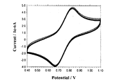
- Example Compound A-1 which is an organic compound of the present invention was subjected to 4-continuous insertion evaluation of 1-electron oxidation using cyclic voltammetry (CV).
- the CV measurement result of Example Compound A-1 is shown in FIG. 1A.
- a reversible oxidation wave was obtained as a result of CV measurement of Example Compound A-1, almost no change in the waveform, and almost no deterioration of Example Compound A-1 due to repeated insertion. There wasn't. This indicates that Exemplified Compound A-1 can exist stably without causing decomposition or reaction due to one-electron oxidation.
- Comparative compound R-2 has a high activity of proton at the ⁇ -position of the thiophene moiety shown below by directly bonding an amino group having higher electron donating property to thiophene having higher electron donating property, and the electrophilic substitution reaction is activated. It is thought that.
- the CV measurement was carried out in a 0.1 M tetrabutylammonium perchlorate ortho-dichlorobenzene solution, using Ag / Ag + for the reference electrode, Pt for the counter electrode, and glassy carbon for the working electrode. Further, the insertion speed was 0.1 V / s.
- As a measuring device model 660C manufactured by ALS, an electrochemical analyzer was used.
- the organic compound of the present invention has high stability against redox reaction and is effective in durability against repeated use of the organic photoelectric conversion element.
- the organic compound layer is preferably produced by a vacuum deposition method. Other methods such as a coating process are also possible.
- a high-purity organic compound layer can be formed by using a vacuum evaporation method.
- an organic photoelectric conversion compound is so preferable that it is high purity.
- the organic compound of the present invention is stable without being decomposed during vacuum deposition or sublimation purification.
- Exemplified Compound A-1 was purified by sublimation at 270 ° C.
- Comparative Compound R-2 decomposed at 280 ° C. without sublimation. This also indicates that the comparative compound R-2 is decomposed during the vacuum deposition and cannot be used in the vacuum deposition process.
- the organic compound of the present invention has high thermal stability and does not decompose in the vacuum deposition process, and can stably produce an organic compound layer.
- the comparative compound R-2 has a high ⁇ -position proton activity due to its high electron donating property and the decomposition reaction is activated, similarly to the reason that the stability to the redox reaction described in (2) is low. Conceivable.
- the organic compound of the present invention Since the organic compound of the present invention has the characteristics shown in the above (1) to (3), it has good panchromic performance, high molar extinction coefficient, high redox stability, and thermal stability. In particular, it can be provided as a compound having high deposition stability. Therefore, the organic compound of the present invention exhibits high vapor deposition stability in the production of the organic photoelectric conversion film and the organic photoelectric conversion element, and is visible when used as a compound layer of the organic photoelectric conversion film and the organic photoelectric conversion element. Good photoelectric conversion characteristics can be obtained in the entire light range.
- FIG. 2 is a schematic cross-sectional view showing an example of the organic photoelectric conversion element of the present invention.
- a first organic compound layer 1 that is a photoelectric conversion unit that converts light into electric charge is disposed between a hole collection electrode 4 and an electron collection electrode 5.
- the first organic compound layer 1 is a layer that receives light and generates a charge corresponding to the amount of light. It can also be called a photoelectric conversion layer because of its function.
- the first organic compound layer 1 has at least the organic compound of the present invention.
- the first organic compound layer 1 may have a plurality of types of organic compounds.
- the first organic compound layer 1 has a plurality of types of organic compounds
- a plurality of types of organic compounds may be mixed in one layer, or a plurality of types of organic compounds may be included in a plurality of layers.
- the plurality of layers are preferably stacked in the direction from the electron collection electrode 5 to the hole collection electrode 4.
- the electron collecting electrode 5 is also called an anode
- the hole collecting electrode 4 is also called a cathode.
- the first organic compound layer 1 is preferably a layer containing an organic p-type semiconductor or an organic n-type semiconductor, and a bulk hetero layer (mixed layer) in which an organic p-type compound and an organic n-type compound are mixed. It is more preferable that at least a part thereof is contained.
- photoelectric conversion efficiency sensitivity
- the first organic compound layer 1 preferably contains fullerene or a fullerene derivative as an organic n-type semiconductor. Since the fullerene or fullerene derivative is continuous in the first organic compound layer 1, an electron path is formed, so that the electron transport property is improved and the high-speed response of the organic photoelectric conversion element is improved.
- the content of fullerene or fullerene derivative is preferably 40% by volume or more and 85% by volume or less with respect to the volume of the first organic compound layer 1.
- fullerenes include fullerene C60, fullerene C70, fullerene C76, fullerene C78, fullerene C80, fullerene C82, fullerene C84, fullerene C90, fullerene C96, fullerene C240, fullerene 540, mixed fullerene, and fullerene nanotubes.
- the fullerene derivative has a substituent on the fullerene, and examples of the substituent include an alkyl group, an aryl group, and an aromatic heterocyclic group.
- the organic p-type semiconductor included in the first organic compound layer 1 is a donor-type organic semiconductor, and is an organic compound that has a property of mainly donating electrons typified by a hole-transporting organic compound.
- the organic photoelectric conversion element of the present invention contains the organic compound of the present invention as an organic p-type semiconductor (electron donor compound).
- the first organic compound layer 1 preferably does not emit light.
- Non-light-emitting means a layer having an emission quantum efficiency of 1% or less, preferably 0.5% or less, more preferably 0.1% or less in the visible light region (wavelength 400 nm to 730 nm).
- the light emission quantum efficiency is 1% or less without affecting the sensing performance or the imaging performance when applied to a sensor or an imaging device.
- the second organic compound layer 2 is a layer that suppresses the flow of electrons from the hole collection electrode 4 to the first organic compound layer 1, and can also be referred to as an electron blocking layer.
- the unoccupied orbit energy is preferably small.
- the organic photoelectric conversion element of the present invention does not necessarily have the second organic compound layer 2.
- the third organic compound layer 3 is a layer that suppresses the flow of holes from the electron collection electrode 5 to the first organic compound layer 1, and can also be referred to as a hole blocking layer, and has a high ionization potential. Is preferred.
- the organic photoelectric conversion element of the present invention does not necessarily have to include the third organic compound layer 3.
- the hole collection electrode 4 is an electrode that collects holes out of the charges generated in the first organic compound layer 1.
- the material constituting the hole collecting electrode 4 is not limited as long as it has high conductivity and transparency. Specific examples include metals, metal oxides, metal nitrides, metal borides, organic conductive compounds, and mixtures thereof. More specifically, tin oxide doped with antimony or fluorine (ATO or FTO). ), Conductive metal oxides such as tin oxide, zinc oxide, indium oxide, indium tin oxide (ITO), indium zinc oxide (IZO), gold, silver, chromium, nickel, titanium, molybdenum, tantalum, tungsten, aluminum, etc.
- conductive compounds such as oxides and nitrides of these metals (for example, titanium nitride (TiN)), a mixture or laminate of these metals and conductive metal oxides, copper iodide, Inorganic conductive materials such as copper sulfide, organic conductive materials such as polyaniline, polythiophene and polypyrrole, and these and ITO or titanium nitride Like laminates of the like.
- the hole collecting electrode 4 is any material of titanium nitride, molybdenum nitride, tantalum nitride, and tungsten nitride.
- the electron collection electrode 5 is an electrode that collects electrons out of the charges generated in the first organic compound layer 1.
- the electron collection electrode 5 is disposed closer to the pixel circuit than the hole collection electrode 4.
- Specific examples of the material constituting the electron collecting electrode 5 include ITO, IZO, SnO 2 , ATO (antimony-doped tin oxide), ZnO, AZO (aluminum-doped zinc oxide), GZO (gallium-doped zinc oxide), and TiO. 2 or any material of FTO (fluorine-doped tin oxide).
- the method for forming the electrode can be appropriately selected in consideration of suitability with the electrode material.
- the electrode may be formed by a wet method such as a printing method or a coating method, a physical method such as a vacuum deposition method, a sputtering method or an ion plating method, or a chemical method such as CVD or plasma CVD method. it can.
- the ITO electrode can be formed by a method such as an electron beam method, a sputtering method, a resistance heating vapor deposition method, a chemical reaction method (sol-gel method or the like), or a dispersion of indium tin oxide.
- the formed ITO electrode can be subjected to UV-ozone treatment, plasma treatment, and the like.
- the electrode is TiN
- various methods including a reactive sputtering method are used, and the formed TiN electrode can be further subjected to annealing treatment, UV-ozone treatment, plasma treatment, and the like.
- the electron collection electrode 5 is connected to the readout circuit 6.
- the readout circuit 6 reads out information based on the charges generated in the organic photoelectric conversion unit composed of the first organic compound layer 1, the second organic compound layer 2, and the third organic compound layer 3, for example, a signal processing unit ( (Not shown) Further, the readout circuit 6 may be connected to the hole collecting electrode 4.
- the organic photoelectric conversion element in FIG. 2 has an inorganic protective layer 7 on the hole collecting electrode 4.
- the inorganic protective layer 7 is made of, for example, silicon oxide, silicon nitride, aluminum oxide, or the like.
- the inorganic protective layer 7 can be formed by a vacuum deposition method, a sputtering method, an atomic layer deposition (ALD) method, or the like.
- a color filter 8 is disposed on the inorganic protective layer 7.
- the color filter 8 include a color filter that transmits red light of visible light.
- one color filter 8 may be disposed for one organic photoelectric conversion element.
- one color filter 8 may be arranged for a plurality of organic photoelectric conversion elements.
- a Bayer arrangement or the like can be used as the arrangement of the color filters 8, a Bayer arrangement or the like can be used.
- a microlens 9 is disposed on the color filter 8.
- the microlens 9 can collect incident light onto the organic photoelectric conversion element.
- one microlens 9 may be arranged for one organic photoelectric conversion element. Or you may have one micro lens 9 with respect to a some organic photoelectric conversion element.
- the organic photoelectric conversion element of the present invention may have a substrate.
- the substrate include a silicon substrate, a glass substrate, and a flexible substrate.
- the organic photoelectric conversion element preferably applies a voltage between the hole collection electrode 4 and the electron collection electrode 5 when performing photoelectric conversion.
- holes may be used for reading as signal charges by reversing the hole collection and electron collection electrodes.
- the organic photoelectric conversion element according to the present invention can be an organic photoelectric conversion element having a different wavelength of received light by appropriately setting the constituent material of the first organic compound layer 1.
- the difference in the wavelength of the received light means that the wavelength range of the light that is photoelectrically converted by the photoelectric conversion unit is different.
- it can also be set as the organic photoelectric conversion apparatus which does not require the color filter 8 by having several organic photoelectric conversion elements from which the wavelength of the light which each receives differs, and laminating
- a plurality of types of organic photoelectric conversion elements included in the organic photoelectric conversion device at least one type of organic photoelectric conversion element is the organic photoelectric conversion element of the present invention.
- the optical area sensor of the present invention has a plurality of photoelectric conversion elements.
- the plurality of photoelectric conversion elements are two-dimensionally arranged in the in-plane direction. In such a configuration, information representing the light intensity distribution in a predetermined light receiving area can be obtained by individually outputting signals based on the charges generated in the plurality of organic photoelectric conversion elements.
- the optical area sensor may have the above-described organic photoelectric conversion device of the present invention instead of the organic photoelectric conversion element of the present invention.
- the image sensor of the present invention has a plurality of organic photoelectric conversion elements each serving as a light receiving pixel, and a transistor connected to each organic photoelectric conversion element.
- the transistor reads the charge generated in the organic photoelectric conversion element, and transmits information based on the read charge to the sensor unit connected to the imaging element.
- Examples of the sensor unit include a CMOS sensor and a CCD sensor. An image can be obtained by collecting the information acquired by each light receiving pixel in the sensor unit.
- FIG. 3 is a schematic diagram showing an example of the image sensor of the present invention.
- the imaging device 501 includes an imaging region 511, a vertical scanning circuit 512, two readout circuits 513, two horizontal scanning circuits 514, and two output amplifiers 515.
- An area other than the imaging area 511 is a circuit area 516.
- the imaging region 511 is configured by arranging a plurality of light receiving pixels in a two-dimensional manner.
- the read circuit 513 includes, for example, a column amplifier, a CDS circuit, an adder circuit, and the like, and amplifies and adds signals read from the pixels in the row selected by the vertical scanning circuit 512 via the vertical signal line. Do.
- the column amplifier, the CDS circuit, the adder circuit, and the like are arranged for each pixel column or a plurality of pixel columns, for example.
- the horizontal scanning circuit 514 generates a signal for sequentially reading the signals of the reading circuit 513.
- the output amplifier 515 amplifies and outputs the signal of the column selected by the horizontal scanning circuit 514.
- the readout circuit 513, the horizontal scanning circuit 514, and the output amplifier 515 are arranged one above the other with the imaging region 511 interposed therebetween in order to configure two output paths. However, three or more output paths may be provided.
- the output signal 521 and the output signal 522 output from each output amplifier 515 are combined as an image signal by the signal processing unit 517.
- FIG. 4 is an example of a pixel drive circuit diagram for driving the light receiving pixels of the image sensor 501.
- the light receiving pixel 100 includes an organic photoelectric conversion element 101.
- the lower surface of the semiconductor layer of the first organic compound layer 1 of the organic photoelectric conversion element 101 is electrically connected to the charge storage unit 115 in the semiconductor substrate and further connected to the amplification unit 103.
- the charge accumulation unit 115 in the Si semiconductor substrate is a region for accumulating charges generated in the organic photoelectric conversion element 101, and a P-type region and an N-type region may be formed.
- the amplification unit 103 can output a signal generated in the organic photoelectric conversion element 101.
- the organic photoelectric conversion element 101 and the amplification unit 103 may be short-circuited.
- FIG. 4 illustrates a node B122 representing the electrical connection between the organic photoelectric conversion element 101 and the amplification unit 103.
- Node B 122 is configured to be electrically floating. When the node B122 is electrically floating, the voltage of the node B122 can be changed according to the electric charge generated in the organic photoelectric conversion element 101. Therefore, a signal corresponding to the charge generated in the organic photoelectric conversion element 101 can be input to the amplification unit 103.
- the light receiving pixel 100 in FIG. 4 includes a reset unit 102 that resets the voltage of the node B122 in the semiconductor substrate.
- the reset unit 102 supplies a reset voltage (not shown) to the node B122.
- the reset unit 102 is, for example, a reset transistor electrically connected to the node B122.
- FIG. 4 illustrates a reset transistor.
- the reset unit 102 is controlled to be switched on and off by a reset control pulse (pRES) 124. When the reset unit 102 is turned on, a reset voltage is supplied to the node B122.
- pRES reset control pulse
- 121 is a common wiring connection (node A)
- 130 is an output line
- 140 is a column circuit
- 160 is a current source
- 104 is a selection transistor for selectively sending a signal to the output line 130.
- the selection transistor 104 is controlled to be switched on and off by a selection transistor drive signal (pSEL) 125.
- the image sensor may have an optical filter such as a color filter.
- an optical filter such as a color filter.
- One optical filter may be provided for one light receiving pixel, or one optical filter may be provided for a plurality of light receiving pixels. Examples of the optical filter include a color filter, a long-pass filter that transmits wavelengths of infrared rays or more, a UV cut filter that transmits wavelengths of ultraviolet rays or less, and a low-pass filter.
- the image sensor may have an optical member such as a microlens.
- the microlens is a lens that collects light from the outside onto the photoelectric conversion unit.
- one optical member may be provided for one light receiving pixel, or one optical member corresponding to a plurality of light receiving pixels may be provided. When a plurality of light receiving pixels are provided, it is preferable that one optical member is provided for each of the plurality of light receiving pixels.
- the imaging apparatus of the present invention includes an imaging optical system having a plurality of lenses and an imaging element that receives light that has passed through the imaging optical system.
- the imaging device may be an imaging device having a joint portion that can be joined to the imaging optical system and an imaging element. More specifically, the imaging device is a digital camera or a digital still camera.
- the imaging device may further include a receiving unit that receives an external signal. The signal received by the receiving unit is a signal that controls at least one of the imaging range of the imaging device, the start of imaging, and the end of imaging.
- the imaging device may further include a transmission unit that transmits the captured image to the outside. By having a receiving unit and a transmitting unit, it can be used as a network camera.
- Examples 4 to 10> In the same manner as in Example 1, except that c-1, c-2, and c-4 were replaced with tertiary amine halides, thiophene boronic acids, and indane derivatives shown in Table 2, respectively, the exemplified compounds shown in Table 2 was synthesized.
- Examples 11 to 19 and Comparative Examples 1 to 3 The compounds d-1 to d-3 used in Examples and Comparative Examples are shown below.
- the compounds R-1 and R-2 used in the comparative examples are the compound R-1 described in Non-Patent Document 1 and the compound R-2 described in Patent Document 1.
- a hole collection electrode 4 On the substrate, a hole collection electrode 4, an electron blocking layer (second organic compound layer 2), a photoelectric conversion layer (first organic compound layer 1), a hole blocking layer (third organic compound layer 3). ) And the electron collecting electrode 5 were produced by the method described below.
- an indium tin oxide film was formed on a Si substrate, and a hole patterning electrode 4 was formed by performing a desired patterning process. At this time, the thickness of the hole collecting electrode 4 was set to 100 nm. Thus, the board
- the organic compound layers 1 to 3 and the electron collecting electrode 5 shown in Table 3 were continuously formed.
- Organic compound layers 1 to 3 were formed by vacuum deposition.
- the exemplified compound A-1 is used as the electron donor material
- the compound d-3 is used as the electron acceptor compound
- the exemplified compound A-1: compound d-3 is in a volume ratio of 25:75. It vapor-deposited like.
- the electrode area of the electron collection electrode 5 facing the hole collection electrode 4 was set to 3 mm 2 . This obtained the organic photoelectric conversion element.
- Example 12 to 19 Comparative Examples 1 to 3
- An organic photoelectric conversion element was obtained by the same method as in Example 11 except that the electron donor material in the first organic compound layer 1 and the material of the second organic compound layer 2 were changed as shown in Table 4. .
- the monochromatic light used for the measurement of the photocurrent density is white light emitted from a xenon lamp (device name: XB-50101AA-A, manufactured by USHIO), a monochromator (device name: MC-10N, It is a monochromatic product made by Ritu Applied Optics). Voltage application to the element and current measurement were performed using a source meter (device name: R6243, manufactured by Advantest). Further, in the measurement of the light absorption rate and the external quantum efficiency inside the device, light was incident perpendicularly to the device and from the upper electrode (electron collecting electrode 5) side.
- the external quantum efficiency at a wavelength of 600 nm of the organic photoelectric conversion elements of Examples 12 to 19 and Comparative Examples 1 to 3 was evaluated according to the following criteria.
- a relative value is a relative value when the external quantum efficiency in wavelength 600nm of the organic photoelectric conversion element of Example 11 is set to 1.
- the results are shown in Table 4.
- the organic compound of the present invention can be produced without decomposing at the time of vapor deposition, and the produced organic photoelectric conversion element is sensitive in the visible light region on the long wavelength side of 600 nm. I understood.
Landscapes
- Chemical & Material Sciences (AREA)
- Organic Chemistry (AREA)
- Physics & Mathematics (AREA)
- Engineering & Computer Science (AREA)
- Materials Engineering (AREA)
- Spectroscopy & Molecular Physics (AREA)
- Electromagnetism (AREA)
- Nanotechnology (AREA)
- Light Receiving Elements (AREA)
- Solid State Image Pick-Up Elements (AREA)
- Plural Heterocyclic Compounds (AREA)
Abstract
本開示は、下記一般式1で示される有機化合物を提供する。一般式1において、部分構造Z1は、骨格中に窒素原子を含んでもよい縮合多環基であって、5員環及び6員環の少なくとも一方を含む縮合多環基を表す。部分構造Z1は、カルボニル基、ジシアノビニリデン基、ハロゲン原子、シアノ基、アルキル基、アルコキシ基、芳香族複素環基またはアリール基を置換基として有しても良い。R1及びR2はアルキル基、アリール基、芳香族複素環基、ハロゲン基、シアノ基を表す。Ar1はアリーレン基または2価の芳香族複素環基を表し、Ar2及びAr3はアリール基または芳香族複素環基を表す。nは1~4の整数を表す。
Description
本発明は、有機化合物並びにそれを有する有機光電変換素子、有機光電変換装置、光エリアセンサ、撮像素子及び撮像装置に関する。
撮像素子には、半導体中に光電変換部位を2次元的に配列して画素とし、各画素の光電変換により発生した信号をCCD回路やCMOS回路により電荷転送、読み出しを行う平面型受光素子が広く用いられている。一方、光電変換部に有機化合物を用いたフォトダイオードが知られている。非特許文献1には、化合物R-1を有機光電変換層に用いた素子の記載がある。特許文献1には、化合物R-2を有機光電変換層に用いた素子の記載がある。

しかし、特許文献1及び非特許文献1に記載の有機化合物は、光吸収の感度、特に長波長側の感度が十分ではない。
Chemical Communications 2012年,48(71)号,P8907-8909.
そこで、本発明は、光吸収の感度が高い有機化合物を提供することを目的とする。
本発明の有機化合物は、下記一般式1で示される。

一般式1において、部分構造Z1は、骨格中に窒素原子を含んでもよい縮合多環基であって、5員環及び6員環の少なくとも一方を含む縮合多環基を表す。部分構造Z1は、カルボニル基、ジシアノビニリデン基、ハロゲン原子、シアノ基、アルキル基、アルコキシ基、芳香族複素環基またはアリール基を置換基として有しても良い。
R1及びR2はアルキル基、アリール基、芳香族複素環基、ハロゲン基、シアノ基を表す。Ar1はアリーレン基または2価の芳香族複素環基を表し、Ar2及びAr3はアリール基または芳香族複素環基を表す。Ar1~Ar3はハロゲン原子、シアノ基、アルキル基、アルコキシ基、芳香族複素環基またはアリール基で置換されてもよい。
nは1~4の整数を表す。
本発明の他の特徴は、添付された図面を参照して各種実施の形態を例示する以下の説明により明らかにされる。
R1及びR2はアルキル基、アリール基、芳香族複素環基、ハロゲン基、シアノ基を表す。Ar1はアリーレン基または2価の芳香族複素環基を表し、Ar2及びAr3はアリール基または芳香族複素環基を表す。Ar1~Ar3はハロゲン原子、シアノ基、アルキル基、アルコキシ基、芳香族複素環基またはアリール基で置換されてもよい。
nは1~4の整数を表す。
本発明の他の特徴は、添付された図面を参照して各種実施の形態を例示する以下の説明により明らかにされる。
本発明の有機化合物は、光吸収の感度、特に長波長側の感度が高い。そのため、有機光電変換素子の光電変換層に好適に用いることができる。
<有機化合物>
本発明の有機化合物は、下記一般式1で示される。
本発明の有機化合物は、下記一般式1で示される。

一般式1において、部分構造Z1は下記に表される構造をいう。部分構造Z1中、*は炭素原子-炭素二重結合が結合する炭素原子を表す。

部分構造Z1は、骨格中に窒素原子を含んでもよい環であって、5員環及び6員環の少なくとも一方を含む縮合多環基を表す。部分構造Z1は、カルボニル基、ジシアノビニリデン基、ハロゲン原子、シアノ基、アルキル基、アルコキシ基、芳香族複素環基またはアリール基を置換基として有しても良い。
部分構造Z1としては、例えば下記一般式11~19で示される構造が挙げられる。
部分構造Z1としては、例えば下記一般式11~19で示される構造が挙げられる。

一般式11~19において、R21~R62は水素原子、ハロゲン原子、シアノ基、アルキル基、アルコキシ基、芳香族複素環基及びアリール基から選ばれる。
一般式11~19におけるR21~R62のハロゲン原子としては、フッ素原子、塩素原子、臭素原子、及びヨウ素原子が挙げられ、フッ素原子が好ましい。
一般式11~19におけるR21~R62のアルキル基としては、メチル基、エチル基、n-プロピル基、iso-プロピル基、n-ブチル基、s-ブチル基、t-ブチル基、オクチル基、1-アダマンチル基、2-アダマンチル基などが挙げられ、メチル基、エチル基、n-プロピル基、iso-プロピル基、n-ブチル基、s-ブチル基、t-ブチル基等の炭素原子数1以上4以下のアルキル基が好ましい。
一般式11~19におけるR21~R62のアルコキシ基としては、メトキシ基、エトキシ基、n-プロポキシ基、iso-プロポキシ基、n-ブトキシ基、s-ブトキシ基、t-ブトキシ基、オクチロキシ基、1-アダマンチルオキシ基、2-アダマンチルオキシ基などが挙げられ、メトキシ基、エトキシ基、n-プロポキシ基、iso-プロポキシ基、n-ブトキシ基、s-ブトキシ基、t-ブトキシ基等の炭素原子数1以上4以下のアルコキシ基が好ましい。
一般式11~19におけるR21~R62の芳香族複素環基としては、ピリジル基、ピラジニル基、ピリジミル基、トリアジニル基、ピロリル基、フラニル基、チエニル基、イミダゾール基、ピラゾール基、オキサゾール基、チアゾール基、イミダゾリニル基、チアジン基、キノリル基、イソキノリル基、アザフェナントレニル基、フェナントロリニル基、ベンゾチエニル基、ジベンゾチエニル基、ベンゾフラニル基、ジベンゾフラニル基などが挙げられ、ピリジル基、ピラジニル基、ピリジミニル基が好ましい。
一般式11~19におけるR21~R62のアリール基としては、フェニル基、ビフェニル基、ターフェニル基、ナフチル基、フェナントレニル基、クリセニル基、ピレニル基、フルオレニル基、フルオランテニル基などが挙げられ、特にフェニル基、ビフェニル基、ナフチル基が好ましい。
上記アルキル基、アルコキシ基、芳香族複素環基、アリール基はさらに置換基を有してもよく、その場合、置換基は、ハロゲン原子、シアノ基、アルキル基、及びアリール基から選ばれる。置換基としてのハロゲン原子は、フッ素原子であることが好ましく、アルキル基は、炭素原子数1以上4以下のアルキル基が好ましく、メチル基、エチル基、iso-プロピル基、s-ブチル基、t-ブチル基が好ましい。アリール基は、フェニル基、ナフチル基、フェナントレニル基、クリセニル基、ピレニル基、フルオレニル基、フルオランテニル基が好ましく、特にフェニル基が好ましい。
一般式1で示される有機化合部中のR1及びR2は水素原子、アルキル基、アリール基、芳香族複素環基、ハロゲン基、シアノ基を表す。アルキル基、アリール基、芳香族複素環基、ハロゲン原子としては、部分構造Z1におけるR21~R62として示した基と同様の基が挙げられる。
一般式1で示される有機化合部中のAr1はアリーレン基または2価の芳香族複素環基を表し、Ar2及びAr3はアリール基または芳香族複素環基を表す。アリーレン基、2価の芳香族複素環基としては、部分構造Z1について説明したアリール基、芳香族複素環基に相当する2価の基が挙げられる。アリール基、芳香族複素環基としては、部分構造Z1について説明したものと同様のものが挙げられる。これらの中でも、Ar1はフェニレン基、ビフェニレン基、またはナフチレン基であることが好ましく、Ar2及びAr3は、それぞれ独立にフェニル基、ビフェニル基、及びナフチル基のいずれか1つであることが好ましい。Ar1~Ar3はハロゲン原子、シアノ基、アルキル基、アルコキシ基、芳香族複素環基またはアリール基を置換基として有しても良い。置換基としてのハロゲン原子、アルキル基、アルコキシ基、芳香族複素環基、アリール基としては、部分構造Z1について説明したものと同様のものが挙げられる。
一般式1において、nはR1及びR2が置換したチオフェン部位の繰り返し数を表す1~4の整数であり、好ましくは1~3の整数、より好ましくは1または2、さらに好ましくは1である。
本発明の有機化合物を以下に例示する。


本発明の有機化合物は、例えば以下のスキームに従って合成することができる。

化合物a-1と化合物a-2の鈴木カップリングにより中間体a-3を合成する。触媒はPd系の触媒が好ましく、特にPdCl2(dppf)2が好ましい。化合物a-1は臭素体以外でもボロン酸と反応する置換基を有すればよく、その他のハロゲン体等でも良い。本発明の有機化合物a-5は中間体a-3と部分構造Z1に対応するケトン体a-4を塩基中で反応させることで合成できる。本発明の有機化合物はこれ以外の合成法でも合成しても良い。以上の方法により様々な本発明の有機化合物a-5が合成できる。
本発明の有機化合物について、例示化合物A-1を例にとり、前述の非特許文献1に記載の化合物R-1、特許文献1に記載の化合物R-2と比較する。
(1)可視光領域の長波長側の吸収(吸収波長及びモル吸光係数)
有機光電変換膜として可視光領域の光を電荷信号としてとらえる場合、380乃至750nmの可視光領域全域において光を吸収できることが好ましい。特に、赤色領域(600乃至750nm)の吸収感度が高いことが好ましい。具体的には、薄膜状態における長波長側の吸収端(吸収スペクトルの立ち上がりの位置)が赤色領域(600nm以上)にあり、クロロホルム希薄溶液(濃度が5×10⁻⁵mol/Lより薄い溶液)中の長波長側の吸収端が580nm以上にあることが好ましく、600nm以上にあることがより好ましい。その場合、クロロホルム希薄溶液の最大吸収波長は、515乃至615nmにあることが好ましい。また、最大吸収波長においてモル吸光係数が高いことが好ましい。
有機光電変換膜として可視光領域の光を電荷信号としてとらえる場合、380乃至750nmの可視光領域全域において光を吸収できることが好ましい。特に、赤色領域(600乃至750nm)の吸収感度が高いことが好ましい。具体的には、薄膜状態における長波長側の吸収端(吸収スペクトルの立ち上がりの位置)が赤色領域(600nm以上)にあり、クロロホルム希薄溶液(濃度が5×10⁻⁵mol/Lより薄い溶液)中の長波長側の吸収端が580nm以上にあることが好ましく、600nm以上にあることがより好ましい。その場合、クロロホルム希薄溶液の最大吸収波長は、515乃至615nmにあることが好ましい。また、最大吸収波長においてモル吸光係数が高いことが好ましい。
表1に、例示化合物A-1と比較化合物R-1及びR-2それぞれのクロロホルム希薄溶液中での最大吸収波長を示した。

比較化合物R-1は、最大吸収波長が507nmであり可視光領域の長波長側を吸収する性能が低く、特に長波長領域の感度を出すことが困難である。一方、例示化合物A1は、532nmであり可視光領域の長波長側を吸収する性能を有し、532nmでのモル吸光係数が高い。これは、電子吸引基による電子吸引性の強さに起因し、電子吸引性の強い基ほどLUMO準位が安定化し吸収スペクトルが長波長化するためである。つまり、比較化合物R-1が有するジシアノ基は本発明の有機化合物が有するケトンを含む縮合多環構造(部分構造Z1)の電子吸引性に比べると電子吸引性が弱いと考えられる。同様に、比較化合物R-2のようなチオフェンがアミノ基に直接結合した化合物も、例示化合物A-1に比べると最大吸収波長はより短波長であり、かつモル吸光係数が非常に低い。
本発明の有機化合物は、吸収スペクトルの端部が長波長側に存在するため、より広い範囲の光を吸収することができる。また、本発明の有機化合物は、モル吸光係数が40000以上であり、高い光吸収の感度を有する化合物である。
また、本発明の有機化合物を有機光電変換素子に用いる場合、フラーレン誘導体等の有機n型半導体を電子アクセプタとして用いることで、本発明の有機化合物が有する吸収領域に加えて特に380nm乃至500nmの短波長側の吸収感度をさらに高めることができる。これにより、パンクロミック性能が良好になる。パンクロミック性能とは、可視光全域において高い吸収感度を有する能力のことである。
さらに、本発明の有機化合物はアミノ基を有することで電子供与性が高い化合物である。また、フラーレン誘導体等の有機n型半導体とともに光電変換層に用いることで電子ドナーとして機能し、良好な光電変換を行う。つまり、パンクロミック性能と良好な光電変換特性により、全波長領域で優れた光電変換特性を有することができる。また、複数の電子ドナー材料とともに用いてもよい。
本発明の有機化合物を光電変換層の電子アクセプタとして電子ドナー材料とともに用いてよい。この場合、電子アクセプタとして、単独または複数種類の本発明の有機化合物を用いることができる。有機光電変換素子においては、電子ドナーと電子アクセプタが光を吸収し電荷分離した後、正孔と電子をそれぞれ電子ドナーと電子アクセプタが電極まで輸送する。複数種類の本発明の有機化合物を光電変換層に混合させた場合、電荷輸送準位にトラップや欠陥を生む場合がある。そのため、複数種類の本発明の有機化合物を光電変換層の電子アクセプタとして用いる場合は、トラップや欠陥を生じにくい本発明の有機化合物の組み合わせとすることが好ましい。
(2)繰り返し使用耐久(酸化還元安定性)
有機光電変換素子は、光を吸収して電荷分離した際にラジカルカチオン種とラジカルアニオン種が生成し、これらが両電極に捕集されなければならない。したがって、特に、本発明の有機化合物をフラーレン誘導体などの有機n型半導体とともに用いる場合は、光吸収化合物としての本発明の有機化合物の酸化還元安定性が高い方が、有機光電変換素子の繰り返し使用耐久性の向上に繋がる。
有機光電変換素子は、光を吸収して電荷分離した際にラジカルカチオン種とラジカルアニオン種が生成し、これらが両電極に捕集されなければならない。したがって、特に、本発明の有機化合物をフラーレン誘導体などの有機n型半導体とともに用いる場合は、光吸収化合物としての本発明の有機化合物の酸化還元安定性が高い方が、有機光電変換素子の繰り返し使用耐久性の向上に繋がる。
本発明の有機化合物である例示化合物A-1を、サイクリックボルタンメトリー(CV)を用いた1電子酸化の4連続挿引評価を行った。例示化合物A-1のCV測定結果を図1Aに示す。図1Aに示されるように、例示化合物A-1のCV測定の結果として可逆な酸化波が得られ、その波形の変化はほぼなく、繰り返し挿引による例示化合物A-1の劣化はほとんど生じていなかった。これは、例示化合物A-1は、一電子酸化による分解や反応を起こすことなく安定に存在できることを示している。一方、比較化合物R-2の1電子酸化の4連続挿引評価を行ったところ、図1Bに示す様に、可逆な酸化波が得られたが、波形の変化が大きく、繰り返し挿引による比較化合物R-2の劣化が生じていると考えられる。比較化合物R-2は電子供与性が高いチオフェンにさらに電子供与性が高いアミノ基が直接結合することで以下に示すチオフェン部位のβ位のプロトンの活性が高く、求電子置換反応が活性化されていると考えられる。

なお、CV測定は、0.1Mテトラブチルアンモニウム過塩素酸塩のオルト-ジクロロベンゼン溶液中で行い、参照電極はAg/Ag+、対極はPt、作用電極はグラッシーカーボンを用いて測定した。また、挿引速度は、0.1V/sで行った。測定装置はALS社製のモデル660C、電気化学アナライザーを用いた。
これより、本発明の有機化合物は、酸化還元反応に対する安定性が高く、有機光電変換素子の繰り返し使用に対する耐久に効果があることが分る。
(3)蒸着安定性
本発明の有機光電変換素子において有機化合物層は真空蒸着法で作製することが好ましい。他にも塗布プロセス等の方式も可能である。真空蒸着法を用いることで純度の高い有機化合物層を形成できる。また、高性能で信頼性の高い有機光電変換素子を実現するためには、有機光電変換化合物は高純度であるほど好ましい。高純度化のためには、昇華精製プロセスを行うことが好ましい。昇華精製により、昇華温度の異なる不純物を除去できるだけでなく無機物等の昇華しない不純物も除去することができるためである。本発明の有機化合物は真空蒸着や昇華精製時に分解することなく安定である。
本発明の有機光電変換素子において有機化合物層は真空蒸着法で作製することが好ましい。他にも塗布プロセス等の方式も可能である。真空蒸着法を用いることで純度の高い有機化合物層を形成できる。また、高性能で信頼性の高い有機光電変換素子を実現するためには、有機光電変換化合物は高純度であるほど好ましい。高純度化のためには、昇華精製プロセスを行うことが好ましい。昇華精製により、昇華温度の異なる不純物を除去できるだけでなく無機物等の昇華しない不純物も除去することができるためである。本発明の有機化合物は真空蒸着や昇華精製時に分解することなく安定である。
例示化合物A-1と比較化合物R-2について昇華精製を試みた。例示化合物A-1は270℃で昇華し精製することができた。しかし、比較化合物R-2は昇華せずに280℃で分解した。このことは、真空蒸着プロセスにおいても同様に、比較化合物R-2は真空蒸着時に分解し、真空蒸着プロセスに対応できないことを表す。一方、本発明の有機化合物は、熱安定性が高く、真空蒸着プロセスにおいて分解せず、安定的に有機化合物層を作製することができる。比較化合物R-2は、上記(2)で説明した酸化還元反応に対する安定性が低い理由と同様に、高い電子供与性によるβ位のプロトンの活性が強まり、分解反応が活性化されていると考えられる。
本発明の有機化合物は、上記(1)~(3)で示した特徴を有するため、パンクロミック性能が良好であり、モル吸光係数が高く、酸化還元安定性が高く、かつ、熱安定性、特に蒸着安定性が高い化合物として提供することができる。したがって、本発明の有機化合物は、有機光電変換膜及び有機光電変換素子の作成の際には高い蒸着安定性を示し、また有機光電変換膜及び有機光電変換素子の化合物層として用いることで、可視光全域において良好な光電変換特性を得ることができる。
<有機光電変換素子>
図2は、本発明の有機光電変換素子の一例を示す断面模式図である。図2の有機光電変換素子は、光を電荷に変換する光電変換部である第一の有機化合物層1が、正孔捕集電極4と電子捕集電極5との間に配置されている。第一の有機化合物層1は、光を受け、その光量に応じた電荷を発生する層である。その機能から光電変換層と呼ぶこともできる。第一の有機化合物層1は、少なくとも本発明の有機化合物を有する。第一の有機化合物層1は、複数種類の有機化合物を有してもよい。第一の有機化合物層1が複数種類の有機化合物を有する場合、複数種類の有機化合物が1つの層に混合されてもよいし、複数種類の有機化合物が、複数の層に含まれてもよい。複数種類の有機化合物が複数の層に含まれている場合、複数の層は、電子捕集電極5から正孔捕集電極4の方向に積層されていることが好ましい。なお、電子捕集電極5はアノードとも呼ばれ、正孔捕集電極4はカソードとも呼ばれる。
図2は、本発明の有機光電変換素子の一例を示す断面模式図である。図2の有機光電変換素子は、光を電荷に変換する光電変換部である第一の有機化合物層1が、正孔捕集電極4と電子捕集電極5との間に配置されている。第一の有機化合物層1は、光を受け、その光量に応じた電荷を発生する層である。その機能から光電変換層と呼ぶこともできる。第一の有機化合物層1は、少なくとも本発明の有機化合物を有する。第一の有機化合物層1は、複数種類の有機化合物を有してもよい。第一の有機化合物層1が複数種類の有機化合物を有する場合、複数種類の有機化合物が1つの層に混合されてもよいし、複数種類の有機化合物が、複数の層に含まれてもよい。複数種類の有機化合物が複数の層に含まれている場合、複数の層は、電子捕集電極5から正孔捕集電極4の方向に積層されていることが好ましい。なお、電子捕集電極5はアノードとも呼ばれ、正孔捕集電極4はカソードとも呼ばれる。
第一の有機化合物層1は、有機p型半導体または有機n型半導体を含有した層であることが好ましく、有機p型化合物と、有機n型化合物とを混合したバルクへテロ層(混合層)を少なくとも一部に含むことがより好ましい。第一の有機化合物層1がバルクへテロ層を有することにより、光電変換効率(感度)を向上させることができる。最適な混合比率でバルクへテロ層を有することにより、第一の有機化合物層1の電子移動度、正孔移動度を高くすることができ、有機光電変換素子の光応答速度を高速にすることができる。
第一の有機化合物層1は、フラーレンまたはフラーレン誘導体を有機n型半導体として含むことが好ましい。フラーレンまたはフラーレン誘導体が第一の有機化合物層1において連なることで、電子の経路が形成されるため、電子輸送性が向上し、有機光電変換素子の高速応答性が向上する。フラーレンまたはフラーレン誘導体の含有量は、第一の有機化合物層1の体積に対して40体積%以上85体積%以下であることが好ましい。フラーレンとしては、例えば、フラーレンC60、フラーレンC70、フラーレンC76、フラーレンC78、フラーレンC80、フラーレンC82、フラーレンC84、フラーレンC90、フラーレンC96、フラーレンC240、フラーレン540、ミックスドフラーレン、フラーレンナノチューブ等が挙げられる。また、フラーレン誘導体は、フラーレンに置換基を有するものであるが、この置換基としては、例えばアルキル基、アリール基、芳香族複素環基等が挙げられる。
第一の有機化合物層1が有する有機p型半導体は、ドナー性有機半導体であり、主に正孔輸送性有機化合物に代表される電子を供与しやすい性質がある有機化合物である。本発明の有機光電変換素子は、有機p型半導体(電子ドナー化合物)として、本発明の有機化合物を含有する。
第一の有機化合物層1は、非発光であることが好ましい。非発光とは、可視光領域(波長400nm~730nm)において発光量子効率が1%以下、好ましくは0.5%以下、より好ましくは0.1%以下の層である。第一の有機化合物層1において、発光量子効率が1%以下であれば、センサや撮像素子に適用した場合にセンシング性能または撮像性能に影響を与えることがなく、好ましい。
図2の有機光電変換素子は、第一の有機化合物層1と正孔捕集電極4の間に配置されている第二の有機化合物層2、及び第一の有機化合物層1と電子捕集電極5との間に配置されている第三の有機化合物層3を有していてもよい。第二の有機化合物層2は、正孔捕集電極4から第一の有機化合物層1へ電子が流れ込むことを抑制する層であり、電子ブロッキング層と呼ぶこともでき、電子親和力あるいはLUMO(最低非占有軌道エネルギー)が小さいことが好ましい。本発明の有機光電変換素子は、第二の有機化合物層2を必ずしも有している必要はない。第三の有機化合物層3は、電子捕集電極5から第一の有機化合物層1へ正孔が流れ込むことを抑制する層であり、正孔ブロッキング層と呼ぶこともでき、イオン化ポテンシャルが高いことが好ましい。本発明の有機光電変換素子は、第三の有機化合物層3を必ずしも有している必要はない。
正孔捕集電極4は、第一の有機化合物層1で発生した電荷のうちの正孔を捕集する電極である。正孔捕集電極4を構成する材料は導電性が高く、透明性を有していれば制限されない。具体的には、金属、金属酸化物、金属窒化物、金属硼化物、有機導電性化合物、これらの混合物等が挙げられ、さらに具体的には、アンチモンまたはフッ素をドープした酸化錫(ATOまたはFTO)、酸化錫、酸化亜鉛、酸化インジウム、酸化インジウム錫(ITO)、酸化亜鉛インジウム(IZO)等の導電性金属酸化物、金、銀、クロム、ニッケル、チタン、モリブデン、タンタル、タングステン、アルミ等の金属及びこれらの金属の酸化物や窒化物などの導電性化合物(一例として窒化チタン(TiN)を挙げる)、さらにこれらの金属と導電性金属酸化物との混合物または積層物、ヨウ化銅、硫化銅などの無機導電性物質、ポリアニリン、ポリチオフェン、ポリピロールなどの有機導電性材料、及びこれらとITOまたは窒化チタンとの積層物などが挙げられる。正孔捕集電極4として特に好ましいのは、窒化チタン、窒化モリブデン、窒化タンタル、窒化タングステンのいずれかの材料である。
電子捕集電極5は、第一の有機化合物層1で発生した電荷のうち電子を捕集する電極である。電子捕集電極5は、正孔捕集電極4よりも画素回路側に配置される。電子捕集電極5を構成する材料として、具体的には、ITO、IZO、SnO2、ATO(アンチモンドープ酸化スズ)、ZnO、AZO(アルミニウムドープ酸化亜鉛)、GZO(ガリウムドープ酸化亜鉛)、TiO2、FTO(フッ素ドープ酸化スズ)のいずれかの材料が挙げられる。
電極を形成する方法は、電極材料との適正を考慮して適宜選択することができる。具体的には、印刷方式、コーティング方式等の湿式方式、真空蒸着法、スパッタリング法、イオンプレーティング法等の物理的方式、CVD、プラズマCVD法等の化学的方式等により電極を形成することができる。電極がITOの場合、電子ビーム法、スパッタリング法、抵抗加熱蒸着法、化学反応法(ゾルーゲル法など)、酸化インジウムスズの分散物の塗布などの方法でITO電極を形成することができる。さらに、形成されたITO電極に、UV-オゾン処理、プラズマ処理などを施すことができる。電極がTiNの場合、反応性スパッタリング法をはじめとする各種の方法が用いられ、形成されたTiN電極に、さらにアニール処理、UV-オゾン処理、プラズマ処理などを施すことができる。
図2の有機光電変換素子では、電子捕集電極5は、読み出し回路6に接続されている。読み出し回路6は、第1の有機化合物層1、第2の有機化合物層2及び第3の有機化合物層3からなる有機光電変換部において発生した電荷に基づく情報を読み出し、例えば、信号処理部(不図示)に伝える。また、読み出し回路6は、正孔捕集電極4に接続されていてもよい。
図2の有機光電変換素子は、正孔捕集電極4の上に無機保護層7を有する。無機保護層7は例えば、酸化シリコン、窒化シリコン、酸化アルミニウム等で構成される。無機保護層7は、真空蒸着法、スパッタリング法、原子層堆積(ALD)法等により形成することができる。
図2の有機光電変換素子では、無機保護層7の上に、カラーフィルタ8が配置されている。カラーフィルタ8は、例えば、可視光のうち赤色の光を透過するカラーフィルタ等があげられる。複数の有機光電変換素子が配置されている場合、1つの有機光電変換素子に対して1つのカラーフィルタ8が配置されてもよい。あるいは、複数の有機光電変換素子に対して1つのカラーフィルタ8が配置されていてもよい。カラーフィルタ8の配列は、ベイヤー配列等を用いることができる。
図2の有機光電変換素子では、カラーフィルタ8の上に、マイクロレンズ9が配置される。マイクロレンズ9は、入射した光を有機光電変換素子へ集光することができる。複数の有機光電変換素子を有する場合、1つの有機光電変換素子に対して1つのマイクロレンズ9が配置されてもよい。あるいは、複数の有機光電変換素子に対して1つのマイクロレンズ9を有してもよい。
本発明の有機光電変換素子は、基板を有していてもよい。基板としては、例えば、シリコン基板、ガラス基板、フレキシブル基板等があげられる。
有機光電変換素子は、光電変換を行う場合に、正孔捕集電極4と電子捕集電極5との間に電圧を加えることが好ましい。また、正孔捕集と電子捕集の電極を逆にすることで信号電荷として正孔を読み出しに用いても良い。
<有機光電変換装置、光エリアセンサ、撮像素子及び撮像装置>
本発明に係る有機光電変換素子は、第一の有機化合物層1の構成材料を適宜設定することで、受光する光の波長が異なる有機光電変換素子とすることができる。受光する光の波長が異なるとは、光電変換部が光電変換する光の波長領域が異なることを意味する。また、それぞれ受光する光の波長が異なる複数の有機光電変換素子を有し、これら複数の有機光電変換素子を積層することで、カラーフィルタ8が必要ない有機光電変換装置とすることもできる。この有機光電変換装置に含まれる複数種類の有機光電変換素子のうち、少なくとも一種類の有機光電変換素子は、本発明の有機光電変換素子である。
本発明に係る有機光電変換素子は、第一の有機化合物層1の構成材料を適宜設定することで、受光する光の波長が異なる有機光電変換素子とすることができる。受光する光の波長が異なるとは、光電変換部が光電変換する光の波長領域が異なることを意味する。また、それぞれ受光する光の波長が異なる複数の有機光電変換素子を有し、これら複数の有機光電変換素子を積層することで、カラーフィルタ8が必要ない有機光電変換装置とすることもできる。この有機光電変換装置に含まれる複数種類の有機光電変換素子のうち、少なくとも一種類の有機光電変換素子は、本発明の有機光電変換素子である。
本発明の光エリアセンサは、光電変換素子を複数有している。複数の光電変換素子は、面内方向に二次元に配置されている。このような構成において、複数の有機光電変換素子で生じた電荷に基づく信号を個別に出力することで、所定の受光エリアにおける光強度の分布を表わす情報を得ることができる。なお、この光エリアセンサは、本発明の有機光電変換素子に換えて、上述した本発明の有機光電変換装置を有してもよい。
本発明の撮像素子は、各々が受光画素となる複数の有機光電変換素子と、それぞれの有機光電変換素子に接続されているトランジスタとを有する。トランジスタは、有機光電変換素子において生じた電荷を読み出し、読み出された電荷に基づく情報を撮像素子に接続されているセンサ部に伝える。センサ部としては、例えば、CMOSセンサやCCDセンサがあげられる。それぞれの受光画素で取得した情報が、センサ部に集められることで画像を得ることができる。
図3は、本発明の撮像素子の一例を示す模式図である。図3において、撮像素子501は、撮像領域511と、垂直走査回路512と、2つの読み出し回路513と、2つの水平走査回路514と、2つの出力アンプ515を備えている。撮像領域511以外の領域が回路領域516である。撮像領域511は、複数の受光画素が2次元状に配列されて構成される。読み出し回路513は、例えば、列アンプ、CDS回路、加算回路等を含み、垂直走査回路512によって選択された行の画素から垂直信号線を介して読み出された信号に対して増幅、加算等を行う。列アンプ、CDS回路、加算回路等は、例えば、画素列または複数の画素列毎に配置される。水平走査回路514は、読み出し回路513の信号を順番に読み出すための信号を生成する。出力アンプ515は、水平走査回路514によって選択された列の信号を増幅して出力する。なお、以上の構成は、本発明の撮像素子の一つの構成例に過ぎず、本発明は、これに限定されるものではない。読み出し回路513と水平走査回路514と出力アンプ515とは、2系統の出力経路を構成するため、撮像領域511を挟んで上下に1つずつ配置されている。しかし、出力経路は3つ以上設けられていてもよい。各出力アンプ515から出力された出力信号521及び出力信号522は信号処理部517で画像信号として合成される。
図4は、撮像素子501の受光画素を駆動する画素駆動回路図の一例である。受光画素100は、有機光電変換素子101を有する。有機光電変換素子101の第一の有機化合物層1の半導体層下面は半導体基板内の電荷蓄積部115に電気的に接続され、さらに増幅部103に接続される。Si半導体基板内の電荷蓄積部115とは、有機光電変換素子101で発生した電荷を蓄積する領域であり、P型領域及びN型領域を形成しても良い。このような構成により、増幅部103が有機光電変換素子101で生じた信号を出力することができる。有機光電変換素子101と増幅部103とは短絡されてもよい。あるいは、図4に示すように有機光電変換素子101と増幅部103との間の電気経路に、スイッチ(転送トランジスタ)105が配されてもよい。スイッチ(転送トランジスタ)105は、転送トランジスタ駆動信号(pTX)123によりオンとオフとが切り替えられるように制御される。図4には、有機光電変換素子101と増幅部103との電気的な接続を表すノードB122が例示されている。ノードB122は、電気的にフローティングとすることが可能となるように構成される。ノードB122が電気的にフローティングになることにより、ノードB122の電圧が有機光電変換素子101で生じた電荷に応じて変化しうる。したがって、増幅部103に有機光電変換素子101で生じた電荷に応じた信号を入力することができる。図4の受光画素100は、半導体基板内のノードB122の電圧をリセットするリセット部102を有する。リセット部102は、リセット電圧(不図示)をノードB122に供給する。リセット部102は、例えば、ノードB122に電気的に接続されたリセットトランジスタである。図4にリセットトランジスタが例示されている。リセット部102は、リセット制御パルス(pRES)124によりオンとオフとが切り替えられるように制御される。リセット部102がオンすることで、ノードB122にリセット電圧が供給される。図4において、121は共通配線接続部(ノードA)、130は出力線、140は列回路、160は電流源であり、104は出力線130へ選択的に信号を送るための選択トランジスタである。選択トランジスタ104は、選択トランジスタ駆動信号(pSEL)125によりオンとオフとが切り替えられるように制御される。
撮像素子は、例えばカラーフィルタ等の光フィルタを有してもよい。有機光電変換素子が、特定の波長の光に対応している場合、有機光電変換素子に対応した光フィルタを有することが好ましい。光フィルタは、1つの受光画素に1つの光フィルタを設けても、複数の受光画素に1つの光フィルタを設けてもよい。光フィルタとしては、カラーフィルタの他に、赤外線以上の波長を透過するロングパスフィルタ、紫外線以下の波長を透過するUVカットフィルタ、ローパスフィルタ等があげられる。
撮像素子は、マイクロレンズ等の光学部材を有してもよい。マイクロレンズは、外部からの光を光電変換部に集光するレンズである。光学部材は、1つの受光画素に1つの光学部材を設けてもよいし、複数の受光画素に対応する1つの光学部材を設けてもよい。受光画素が複数設けられている場合は、複数の受光画素のそれぞれに1つずつ光学部材が設けられることが好ましい。
本発明の撮像装置は、複数のレンズを有する撮像光学系と、撮像光学系を通過した光を受光する撮像素子と、を有する。また、撮像装置は、撮像光学系と接合可能な接合部と、撮像素子とを有する撮像装置であってもよい。撮像装置はより具体的には、デジタルカメラまたはデジタルスチルカメラである。また、撮像装置は、外部からの信号をする受信部をさらに有してもよい。受信部が受信する信号は、撮像装置の撮像範囲、撮像の開始、撮像の終了の少なくともいずれかを制御する信号である。また、撮像装置は、撮像した画像を外部に送信する送信部をさらに有してもよい。受信部や送信部を有することで、ネットーワークカメラとして用いることができる。
以下、実施例により本発明をより詳細に説明するが、本発明の技術的範囲は以下に説明する実施例に限定されるものではない。
<実施例1>
以下のスキームに従って例示化合物A-1を合成した。
以下のスキームに従って例示化合物A-1を合成した。
[中間体c-3の合成]

100ml三ツ口フラスコに、化合物c-1 1.62g(5.0mmol)、化合物c-2 1.56g(10.0mmol)、炭酸カリウム3.45g、トルエン35ml、メタノール35mlを入れ、窒素雰囲気中、室温で攪拌下、ジフェニルホスフィノフェロセンパラジウムジクロリド0.18gを添加した。その後反応温度を90度に昇温し、5時間攪拌した。反応後、有機層をトルエンで抽出し無水硫酸ナトリウムで乾燥後、シリカゲルカラム(展開溶媒:クロロホルムとヘプタンの混合溶媒)で精製し、化合物c-3(黄色固体)1.21g(収率68%)を得た。
[例示化合物A-1の合成]

100ml三ツ口フラスコに、化合物c-3 1.20g(3.38mmol)、化合物c-4 0.59g(4.06mmol)、エタノール100mlを入れ、窒素雰囲気中、室温で攪拌下、ピペリジン0.05mlを添加した。その後反応温度を90度に昇温し、5時間攪拌した。室温まで冷却後、ろ過し、エタノールで洗浄した。シリカゲルカラム(展開溶媒:クロロホルムとヘプタンの混合溶媒)で精製し、例示化合物A-1(赤紫色固体)1.34g(収率82%)を得た。質量分析法により、例示化合物A-1のM+である483を確認した。
<実施例2>
以下のスキームに従って例示化合物A-2を合成した。
以下のスキームに従って例示化合物A-2を合成した。
[中間体c-8の合成]

100ml三ツ口フラスコに、化合物c-6 5.60g(20.0mmol)、化合物c-7 6.70g(24.0mmol)、ナトリウム t-ブトキシド3.84g(40.0mmol)、トルエン120mlを入れ、窒素雰囲気中、室温で攪拌下、1、1’-ビス(ジフェニルホスフィノ)フェロセン0.55g、酢酸パラジウム0.12gを添加した。その後反応温度を85度に昇温し、6時間攪拌した。反応後、有機層をトルエンで抽出し無水硫酸ナトリウムで乾燥後、シリカゲルカラム(展開溶媒:トルエンとヘプタンの混合溶媒)で精製し、化合物c-8(白色固体)5.75g(収率66%)を得た。
[中間体c-9の合成]

100ml三ツ口フラスコに、化合物c-8 2.18g(5.0mmol)、化合物c-2 1.56g(10.0mmol)、炭酸カリウム3.45g、トルエン35ml、メタノール35mlを入れ、窒素雰囲気中、室温で攪拌下、1、1’-ビス(ジフェニルホスフィノ)フェロセンパラジウムジクロリド0.18gを添加した。その後反応温度を90度に昇温し、6時間攪拌した。反応後、有機層をトルエンで抽出し無水硫酸ナトリウムで乾燥後、シリカゲルカラム(展開溶媒:クロロホルムとヘプタンの混合溶媒)で精製し、化合物c-9(黄色結晶)1.47g(収率63%)を得た。
[例示化合物A-2の合成]

100ml三ツ口フラスコに、化合物c-3 0.93g(2.0mmol)、化合物c-4 0.35g(2.4mmol)、エタノール30mlを入れ、窒素雰囲気中、室温で攪拌下、ピペリジン0.05mlを添加した。その後反応温度を90度に昇温し、5時間攪拌した。室温まで冷却後、ろ過し、エタノールで洗浄した。シリカゲルカラム(展開溶媒:クロロホルムとヘプタンの混合溶媒)で精製し、例示化合物A-2(赤紫色固体)0.92g(収率77%)を得た。質量分析法により、例示化合物A-2のM+である595を確認した。
<実施例3>
以下のスキームに従って例示化合物A-10を合成した。
以下のスキームに従って例示化合物A-10を合成した。
[中間体c-11の合成]

100ml三ツ口フラスコに、化合物c-10 2.50g(13.6mmol)、無水酢酸10mlを入れ、窒素雰囲気中、室温で攪拌下トリエチルアミン 3.00gを滴下後、アセト酢酸エチル 1.90g(15.0mmol)をゆっくり滴下した。室温で5時間攪拌した。その後氷冷却後、氷7gを添加し、濃塩酸6mlをゆっくり滴下した。室温で3時間攪拌した後、60度で1時間攪拌した。室温まで冷却後、ろ過し、水、アセトンの順に洗浄し、化合物c-11(白黄色固体)1.77g(収率77%)を得た。
[例示化合物A-10の合成]

100ml三ツ口フラスコに、化合物c-9 0.47g(1.0mmol)、化合物c-11 0.27g(1.5mmol)、エタノール20mlを入れ、窒素雰囲気中、室温で攪拌下、ピペリジン0.03mlを添加した。その後反応温度を90度に昇温し、5時間攪拌した。室温まで冷却後、ろ過し、エタノールで洗浄した。シリカゲルカラム(展開溶媒:トルエンとヘプタンの混合溶媒)で精製し、例示化合物A-10(赤紫色結晶)0.23g(収率36%)を得た。質量分析法により、例示化合物A-10のM+である631を確認した。
<実施例4乃至10>
実施例1において、c-1、c-2、c-4を、それぞれ表2に示す3級アミンハロゲン体、チオフェンボロン酸、インダン誘導体に置き換えた以外は同様にして、表2に示す例示化合物を合成した。
実施例1において、c-1、c-2、c-4を、それぞれ表2に示す3級アミンハロゲン体、チオフェンボロン酸、インダン誘導体に置き換えた以外は同様にして、表2に示す例示化合物を合成した。

<実施例11乃至19、比較例1乃至3>
以下に実施例・比較例で使用した化合物d-1~d-3を示す。なお、比較例において使用した化合物R-1、R-2は、前述の非特許文献1に記載の化合物R-1、特許文献1に記載の化合物R-2である。
以下に実施例・比較例で使用した化合物d-1~d-3を示す。なお、比較例において使用した化合物R-1、R-2は、前述の非特許文献1に記載の化合物R-1、特許文献1に記載の化合物R-2である。

[実施例11]
基板の上に、正孔捕集電極4、電子ブロッキング層(第二の有機化合物層2)、光電変換層(第一の有機化合物層1)、正孔ブロッキング層(第三の有機化合物層3)及び電子捕集電極5が、この順で形成されている光電変換素子を、以下に説明する方法により作製した。
基板の上に、正孔捕集電極4、電子ブロッキング層(第二の有機化合物層2)、光電変換層(第一の有機化合物層1)、正孔ブロッキング層(第三の有機化合物層3)及び電子捕集電極5が、この順で形成されている光電変換素子を、以下に説明する方法により作製した。
まずSi基板の上に、インジウムスズ酸化物を成膜し、所望のパターニング加工を施すことにより正孔捕集電極4を形成した。このとき正孔捕集電極4の膜厚を100nmとした。このように正孔捕集電極4が形成された基板を電極付基板として、以下の工程で使用した。
上記電極付基板の上に、表3に示される有機化合物層1~3及び電子捕集電極5を連続成膜した。有機化合物層1~3は真空蒸着法で形成した。第一の有機化合物層1においては、電子ドナー材料として例示化合物A-1を、電子アクセプタ化合物として化合物d-3を、例示化合物A-1:化合物d-3が体積比で25:75となる様に蒸着した。なお、正孔捕集電極4と対向する電子捕集電極5の電極面積が3mm2となるようにした。これにより有機光電変換素子を得た。

[実施例12乃至19、比較例1乃至3]
第一の有機化合物層1中の電子ドナー材料及び第二の有機化合物層2の材料を、表4に示す通りに変更した以外は、実施例11と同様の方法により有機光電変換素子を得た。
第一の有機化合物層1中の電子ドナー材料及び第二の有機化合物層2の材料を、表4に示す通りに変更した以外は、実施例11と同様の方法により有機光電変換素子を得た。

[有機光電変換素子の評価]
得られた素子について、5Vの電圧を印加し、その際の外部量子効率を測定した。外部量子効率は素子に対して、正孔捕集電極4と電子捕集電極5との間に、5Vの電圧を印加した状態で、各波長に対応した、強度50μW/cm2の単色光を素子へ照射した時に流れる光電流密度を測定することで算出した。ここで、光電流密度は、光照射時の電流密度から、遮光時での暗電流密度を差し引いて求めた。なお、光電流密度の測定の際に用いた単色光は、キセノンランプ(装置名:XB-50101AA-A、ウシオ電機製)から出射される白色光を、モノクロメータ(装置名:MC-10N、リツー応用光学製)で単色化したものである。素子への電圧印加及び電流計測は、ソースメータ(装置名:R6243、アドバンテスト製)を用いて行った。また、素子内部の光吸収率及び外部量子効率の測定において、光の入射は、素子に対して垂直に、かつ上部電極(電子捕集電極5)側から行った。
得られた素子について、5Vの電圧を印加し、その際の外部量子効率を測定した。外部量子効率は素子に対して、正孔捕集電極4と電子捕集電極5との間に、5Vの電圧を印加した状態で、各波長に対応した、強度50μW/cm2の単色光を素子へ照射した時に流れる光電流密度を測定することで算出した。ここで、光電流密度は、光照射時の電流密度から、遮光時での暗電流密度を差し引いて求めた。なお、光電流密度の測定の際に用いた単色光は、キセノンランプ(装置名:XB-50101AA-A、ウシオ電機製)から出射される白色光を、モノクロメータ(装置名:MC-10N、リツー応用光学製)で単色化したものである。素子への電圧印加及び電流計測は、ソースメータ(装置名:R6243、アドバンテスト製)を用いて行った。また、素子内部の光吸収率及び外部量子効率の測定において、光の入射は、素子に対して垂直に、かつ上部電極(電子捕集電極5)側から行った。
実施例12乃至19、比較例1乃至3の有機光電変換素子の、波長600nmでの外部量子効率を、下記基準により評価した。なお、相対値とは、実施例11の有機光電変換素子の、波長600nmでの外部量子効率を1としたときの相対値である。結果を表4に示す。
A:外部量子効率の相対値が0.9以上である場合
B:外部量子効率の相対値が0.7以上0.9未満である場合
C:外部量子効率の相対値が0.7未満である場合
A:外部量子効率の相対値が0.9以上である場合
B:外部量子効率の相対値が0.7以上0.9未満である場合
C:外部量子効率の相対値が0.7未満である場合
表4に示される結果より、本発明の有機化合物は蒸着時に分解することなく、素子作成が可能であり、作製した有機光電変換素子は、600nmの長波長側の可視光領域に感度があることが分かった。
この出願は2016年7月21日に出願された日本国特許出願番号2016-143317の優先権を主張するものであり、それらの内容を引用してこの出願の一部とするものである。
1 第一の有機化合物層
2 第二の有機化合物層
3 第三の有機化合物層
4 正孔捕集電極
5 電子捕集電極
6 読み出し回路
7 無機保護層
8 カラーフィルタ
9 マイクロレンズ
501 撮像素子
511 撮像領域
512 垂直走査回路
513 読み出し回路
514 水平走査回路
515 出力アンプ
516 回路領域
517 信号処理部
521 出力信号
522 出力信号
100 受光画素
101 有機光電変換素子
102 リセット部
103 増幅部
104 選択トランジスタ
105 スイッチ(転送トランジスタ)
121 共通配線接続部(ノードA)
122 ノードB
123 転送トランジスタ駆動信号(pTX)
124 リセット制御パルス(pRES)
125 選択トランジスタ駆動信号(pSEL)
130 出力線
140 列回路
160 電流源
Claims (18)
- 下記一般式1で示される有機化合物。

R1及びR2はアルキル基、アリール基、芳香族複素環基、ハロゲン基、シアノ基を表す。Ar1はアリーレン基または2価の芳香族複素環基を表し、Ar2及びAr3はアリール基または芳香族複素環基を表す。Ar1~Ar3はハロゲン原子、シアノ基、アルキル基、アルコキシ基、芳香族複素環基またはアリール基を置換基として有しても良い。
nは1~4の整数を表す。 - 前記一般式1において、部分構造Z1が下記一般式11~19のいずれか1つで示される構造である請求項1に記載の有機化合物。

- 前記一般式1において、Ar1はフェニレン基、ビフェニレン基、またはナフチレン基であり、Ar2及びAr3は、それぞれ独立にフェニル基、ビフェニル基、及びナフチル基のいずれか1つである請求項1または2に記載の有機化合物。
- 電子捕集電極と、正孔捕集電極と、前記電子捕集電極と前記正孔捕集電極との間に配置されている光電変換部と、を有する有機光電変換素子であって、
前記光電変換部は、請求項1乃至3のいずれか一項に記載の有機化合物を少なくとも有する有機化合物層を有する有機光電変換素子。 - 前記有機化合物層が、有機n型半導体を有する請求項4に記載の有機光電変換素子。
- 前記有機n型半導体が、フラーレンまたはフラーレン誘導体である請求項5に記載の有機光電変換素子。
- 請求項4乃至6のいずれか一項に記載の有機光電変換素子を複数有し、前記有機光電変換素子が面内方向に二次元に配置されている光エリアセンサ。
- 受光する光の波長が異なる複数種類の有機光電変換素子を有し、
前記複数種類の有機光電変換素子のうち少なくとも一種類の有機光電変換素子が請求項4乃至6のいずれか一項に記載の有機光電変換素子であり、
前記複数種類の有機光電変換素子が積層されている有機光電変換装置。 - 請求項8に記載の光電変換装置を複数有し、前記光電変換装置が面内方向に二次元に配置されている光エリアセンサ。
- 複数の有機光電変換素子と、前記有機光電変換素子のそれぞれに接続されるトランジスタとを有し、
前記有機光電変換素子が請求項4乃至6のいずれか一項に記載の有機光電変換素子であり、
前記有機光電変換素子のそれぞれが受光画素である撮像素子。 - 前記受光画素に対応した光フィルタを有する請求項10に記載の撮像素子。
- 前記光フィルタが、赤外線以上の波長を透過するロングパスフィルタ、紫外線以下の波長を透過するローパスフィルタのいずれかである請求項11に記載の撮像素子。
- 複数の前記受光画素のそれぞれに対応して配置されている光学部材を有する請求項10乃至12のいずれか一項に記載の撮像素子。
- 撮像光学系と、前記撮像光学系を通過した光を受光する撮像素子とを有し、前記撮像素子は、請求項10乃至13のいずれか一項に記載の撮像素子である撮像装置。
- 前記撮像光学系と接合可能な接合部を有する請求項14に記載の撮像装置。
- デジタルカメラまたはデジタルスチルカメラである請求項14または15に記載の撮像装置。
- 外部からの信号を受信する受信部を有し、前記信号が、撮像範囲、撮像の開始及び撮像の終了のいずれかを制御する信号である請求項14乃至16のいずれか一項に記載の撮像装置。
- 取得した画像を外部に送信する送信部を有する請求項14乃至17のいずれか一項に記載の撮像装置。
Priority Applications (1)
| Application Number | Priority Date | Filing Date | Title |
|---|---|---|---|
| US16/243,500 US10978644B2 (en) | 2016-07-21 | 2019-01-09 | Organic compound and organic photoelectric conversion element including the same |
Applications Claiming Priority (2)
| Application Number | Priority Date | Filing Date | Title |
|---|---|---|---|
| JP2016-143317 | 2016-07-21 | ||
| JP2016143317A JP2018014426A (ja) | 2016-07-21 | 2016-07-21 | 有機化合物及びそれを有する有機光電変換素子 |
Related Child Applications (1)
| Application Number | Title | Priority Date | Filing Date |
|---|---|---|---|
| US16/243,500 Continuation US10978644B2 (en) | 2016-07-21 | 2019-01-09 | Organic compound and organic photoelectric conversion element including the same |
Publications (1)
| Publication Number | Publication Date |
|---|---|
| WO2018016354A1 true WO2018016354A1 (ja) | 2018-01-25 |
Family
ID=60992970
Family Applications (1)
| Application Number | Title | Priority Date | Filing Date |
|---|---|---|---|
| PCT/JP2017/024986 WO2018016354A1 (ja) | 2016-07-21 | 2017-07-07 | 有機化合物及びそれを有する有機光電変換素子 |
Country Status (3)
| Country | Link |
|---|---|
| US (1) | US10978644B2 (ja) |
| JP (2) | JP2018014426A (ja) |
| WO (1) | WO2018016354A1 (ja) |
Cited By (6)
| Publication number | Priority date | Publication date | Assignee | Title |
|---|---|---|---|---|
| US10861903B2 (en) | 2017-08-07 | 2020-12-08 | Canon Kabushiki Kaisha | Organic compound and photoelectric conversion element |
| US10868260B2 (en) | 2017-09-20 | 2020-12-15 | Canon Kabushiki Kaisha | Organic compound and photoelectric conversion element |
| US10873032B2 (en) | 2016-03-03 | 2020-12-22 | Canon Kabushiki Kaisha | Organic photoelectric conversion element, two-dimensional sensor, image sensor, and imaging apparatus |
| US10978644B2 (en) | 2016-07-21 | 2021-04-13 | Canon Kabushiki Kaisha | Organic compound and organic photoelectric conversion element including the same |
| US11555028B2 (en) | 2017-10-25 | 2023-01-17 | Canon Kabushiki Kaisha | Organic compound and photoelectric conversion element |
| US11895910B2 (en) | 2017-08-23 | 2024-02-06 | Canon Kabushiki Kaisha | Organic compound and photoelectric conversion element |
Families Citing this family (1)
| Publication number | Priority date | Publication date | Assignee | Title |
|---|---|---|---|---|
| EP3582275B1 (en) | 2017-02-07 | 2023-09-06 | Canon Kabushiki Kaisha | Photoelectric conversion element, optical area sensor using same, imaging element, and imaging device |
Citations (12)
| Publication number | Priority date | Publication date | Assignee | Title |
|---|---|---|---|---|
| JP2003238559A (ja) * | 2002-02-08 | 2003-08-27 | Mitsui Chemicals Inc | アミン化合物 |
| JP2005008558A (ja) * | 2003-06-19 | 2005-01-13 | Mitsui Chemicals Inc | 五員環化合物、および該五員環化合物を含有する有機電界発光素子 |
| JP2006063043A (ja) * | 2004-08-30 | 2006-03-09 | Mitsui Chemicals Inc | アミノ置換テトラフェニルチオフェン化合物、および該化合物を含有する有機電界発光素子 |
| JP2007091714A (ja) * | 2005-09-27 | 2007-04-12 | Samsung Electronics Co Ltd | 新規な窒素系半導体化合物並びにこれを用いた有機薄膜トランジスタ、有機太陽光電池および有機電界発光素子 |
| JP2007201408A (ja) * | 2005-12-26 | 2007-08-09 | Fuji Xerox Co Ltd | 有機電界発光素子 |
| JP2009079092A (ja) * | 2007-09-25 | 2009-04-16 | Mitsui Chemicals Inc | 高分子化合物、および該高分子化合物を含有する有機電界発光素子 |
| CN101787020A (zh) * | 2010-03-24 | 2010-07-28 | 吉林大学 | 一种可溶液加工的有机共轭分子及在太阳能电池中的应用 |
| JP2011500882A (ja) * | 2007-10-15 | 2011-01-06 | 東進セミケム株式会社 | 新規なチオフェン系染料及びその製造方法 |
| CN101962380A (zh) * | 2010-09-13 | 2011-02-02 | 吉林大学 | 一种新型有机共轭分子及其在有机太阳能电池中的应用 |
| JP2012051854A (ja) * | 2010-09-03 | 2012-03-15 | Toyo Ink Sc Holdings Co Ltd | インダノン誘導体とその色素増感型太陽電池用色材としての利用 |
| WO2013168084A1 (de) * | 2012-05-10 | 2013-11-14 | Heliatek Gmbh | Optoelektronische baulemente mit organischem lochtransportmaterial |
| WO2016066494A1 (en) * | 2014-10-31 | 2016-05-06 | Basf Se | Hole-transport materials for organic solar cells or organic optical sensors |
Family Cites Families (11)
| Publication number | Priority date | Publication date | Assignee | Title |
|---|---|---|---|---|
| US20060119724A1 (en) * | 2004-12-02 | 2006-06-08 | Fuji Photo Film Co., Ltd. | Imaging device, signal processing method on solid-state imaging element, digital camera and controlling method therefor and color image data generating method |
| JP5217475B2 (ja) * | 2008-02-07 | 2013-06-19 | コニカミノルタビジネステクノロジーズ株式会社 | 光電変換素子及び太陽電池 |
| JP2009269987A (ja) * | 2008-05-07 | 2009-11-19 | Konica Minolta Business Technologies Inc | 新規化合物、光電変換素子及び太陽電池 |
| EP2786983A1 (en) * | 2009-09-08 | 2014-10-08 | Fujifilm Corporation | Compounds for use in a photoelectric conversion material, and intermediates for the preparation thereof |
| JP5520560B2 (ja) | 2009-09-29 | 2014-06-11 | 富士フイルム株式会社 | 光電変換素子、光電変換素子材料、光センサ、及び撮像素子 |
| JP2015065267A (ja) * | 2013-09-25 | 2015-04-09 | 東洋インキScホールディングス株式会社 | 有機薄膜太陽電池素子用材料およびその用途 |
| JP6206037B2 (ja) * | 2013-09-26 | 2017-10-04 | 株式会社リコー | 光電変換素子 |
| JP6777983B2 (ja) * | 2014-11-04 | 2020-10-28 | 三星電子株式会社Samsung Electronics Co.,Ltd. | 有機光電素子用化合物及びこれを含む有機光電素子並びにイメージセンサー及び電子装置 |
| WO2016190217A1 (ja) * | 2015-05-28 | 2016-12-01 | ソニーセミコンダクタソリューションズ株式会社 | 光電変換素子および固体撮像装置ならびに電子機器 |
| JP6645700B2 (ja) | 2016-03-03 | 2020-02-14 | キヤノン株式会社 | 有機光電変換素子、二次元センサ、画像センサ及び撮像装置 |
| JP2018014426A (ja) | 2016-07-21 | 2018-01-25 | キヤノン株式会社 | 有機化合物及びそれを有する有機光電変換素子 |
-
2016
- 2016-07-21 JP JP2016143317A patent/JP2018014426A/ja active Pending
-
2017
- 2017-07-07 WO PCT/JP2017/024986 patent/WO2018016354A1/ja active Application Filing
-
2019
- 2019-01-09 US US16/243,500 patent/US10978644B2/en active Active
-
2021
- 2021-11-04 JP JP2021179948A patent/JP7379444B2/ja active Active
Patent Citations (12)
| Publication number | Priority date | Publication date | Assignee | Title |
|---|---|---|---|---|
| JP2003238559A (ja) * | 2002-02-08 | 2003-08-27 | Mitsui Chemicals Inc | アミン化合物 |
| JP2005008558A (ja) * | 2003-06-19 | 2005-01-13 | Mitsui Chemicals Inc | 五員環化合物、および該五員環化合物を含有する有機電界発光素子 |
| JP2006063043A (ja) * | 2004-08-30 | 2006-03-09 | Mitsui Chemicals Inc | アミノ置換テトラフェニルチオフェン化合物、および該化合物を含有する有機電界発光素子 |
| JP2007091714A (ja) * | 2005-09-27 | 2007-04-12 | Samsung Electronics Co Ltd | 新規な窒素系半導体化合物並びにこれを用いた有機薄膜トランジスタ、有機太陽光電池および有機電界発光素子 |
| JP2007201408A (ja) * | 2005-12-26 | 2007-08-09 | Fuji Xerox Co Ltd | 有機電界発光素子 |
| JP2009079092A (ja) * | 2007-09-25 | 2009-04-16 | Mitsui Chemicals Inc | 高分子化合物、および該高分子化合物を含有する有機電界発光素子 |
| JP2011500882A (ja) * | 2007-10-15 | 2011-01-06 | 東進セミケム株式会社 | 新規なチオフェン系染料及びその製造方法 |
| CN101787020A (zh) * | 2010-03-24 | 2010-07-28 | 吉林大学 | 一种可溶液加工的有机共轭分子及在太阳能电池中的应用 |
| JP2012051854A (ja) * | 2010-09-03 | 2012-03-15 | Toyo Ink Sc Holdings Co Ltd | インダノン誘導体とその色素増感型太陽電池用色材としての利用 |
| CN101962380A (zh) * | 2010-09-13 | 2011-02-02 | 吉林大学 | 一种新型有机共轭分子及其在有机太阳能电池中的应用 |
| WO2013168084A1 (de) * | 2012-05-10 | 2013-11-14 | Heliatek Gmbh | Optoelektronische baulemente mit organischem lochtransportmaterial |
| WO2016066494A1 (en) * | 2014-10-31 | 2016-05-06 | Basf Se | Hole-transport materials for organic solar cells or organic optical sensors |
Non-Patent Citations (5)
| Title |
|---|
| GUPTA AKHIL ET AL.: "Molecular engineering for panchromatic absorbing oligothiophene donor-pi-acceptor organic semiconductors", TETRAHEDRON, vol. 68, no. 46, 2012, pages 9440 - 9447, XP028943858, ISSN: 0040-4020, DOI: 10.1016/j.tet.2012.09.009 * |
| HIRADE MASAYA ET AL.: "Effects of Intramolecular Donor-Acceptor Interactions on Bimolecular Recombination in Small-Molecule Organic Photovoltaic Cells", JOURNAL OF PHYSICAL CHEMISTRY C, vol. 117, no. 10, 2013, pages 4986 - 4991, XP055602451, ISSN: 1932-7447, DOI: 10.1021/jp400386q * |
| LERICHE PHILIPPE ET AL.: "Molecular Engineering of the Inter nal Charge Transfer in Thiophene-Triphenylamine Hybrid pi'Co njugated Systems", JOURNAL OF ORGANIC CHEMISTRY, vol. 72, no. 22, October 2007 (2007-10-01), pages 8332 - 8336, XP055446969, ISSN: 0022-3263, DOI: 10.1021/jo701390y * |
| QI CHUNXUAN ET AL.: "Study of Red-Emission Piezochromic Mate rials Based on Triphenylamine", CHEMPLUSCHEM, vol. 81, no. 7, 25 May 2016 (2016-05-25) - 17 June 2016 (2016-06-17), pages 637 - 645, XP055602447, ISSN: 2192-6506, DOI: 10.1002/cplu.201600104 * |
| ROQUET SOPHIE ET AL.: "Triphenylamine-Thienylenevinylene Hybrid Systems with Internal Charge Transfer as Donor Materials for Heterojunction Solar Cells", JOURNAL OF THE AMERICAN CHE MICAL SOCIETY, vol. 128, no. 10, 2006, pages 3459 - 3466, XP002397900, ISSN: 0002-7863, DOI: 10.1021/ja058178e * |
Cited By (7)
| Publication number | Priority date | Publication date | Assignee | Title |
|---|---|---|---|---|
| US10873032B2 (en) | 2016-03-03 | 2020-12-22 | Canon Kabushiki Kaisha | Organic photoelectric conversion element, two-dimensional sensor, image sensor, and imaging apparatus |
| US10978644B2 (en) | 2016-07-21 | 2021-04-13 | Canon Kabushiki Kaisha | Organic compound and organic photoelectric conversion element including the same |
| US10861903B2 (en) | 2017-08-07 | 2020-12-08 | Canon Kabushiki Kaisha | Organic compound and photoelectric conversion element |
| US11895910B2 (en) | 2017-08-23 | 2024-02-06 | Canon Kabushiki Kaisha | Organic compound and photoelectric conversion element |
| US10868260B2 (en) | 2017-09-20 | 2020-12-15 | Canon Kabushiki Kaisha | Organic compound and photoelectric conversion element |
| US11793074B2 (en) | 2017-09-20 | 2023-10-17 | Canon Kabushiki Kaisha | Organic compound and photoelectric conversion element |
| US11555028B2 (en) | 2017-10-25 | 2023-01-17 | Canon Kabushiki Kaisha | Organic compound and photoelectric conversion element |
Also Published As
| Publication number | Publication date |
|---|---|
| JP7379444B2 (ja) | 2023-11-14 |
| JP2018014426A (ja) | 2018-01-25 |
| JP2022021347A (ja) | 2022-02-02 |
| US20190148644A1 (en) | 2019-05-16 |
| US10978644B2 (en) | 2021-04-13 |
Similar Documents
| Publication | Publication Date | Title |
|---|---|---|
| WO2018016354A1 (ja) | 有機化合物及びそれを有する有機光電変換素子 | |
| WO2017149958A1 (ja) | 有機光電変換素子、二次元センサ、画像センサ及び撮像装置 | |
| KR20110028234A (ko) | 광전 변환 소자 및 그 제조방법, 광센서, 촬상소자 및 이들의 구동방법 | |
| JP6833351B2 (ja) | 有機光電変換素子、光エリアセンサ、撮像素子および撮像装置 | |
| JP6029606B2 (ja) | 光電変換素子、撮像素子、光センサ、光電変換素子の使用方法 | |
| EP3466937B1 (en) | Photoelectric conversion element, two-dimensional sensor, image sensor and imaging device | |
| JP7013163B2 (ja) | 有機化合物及び光電変換素子 | |
| JP6932564B2 (ja) | 有機光電変換素子、撮像素子及び撮像装置 | |
| JP2018020976A (ja) | 有機化合物及びこれを用いた光電変換素子、光エリアセンサ、光電変換装置、撮像素子、撮像装置 | |
| JP2019055919A (ja) | 有機化合物及び光電変換素子 | |
| JP7051332B2 (ja) | 有機化合物及び光電変換素子 | |
| JP7016662B2 (ja) | 有機化合物、それを用いた光電変換素子および撮像装置 | |
| JP7177001B2 (ja) | ジベンゾピロメテンホウ素キレート化合物、近赤外光吸収色素、光電変換素子、近赤外光センサー及び撮像素子 | |
| JP7177002B2 (ja) | ジベンゾピロメテンホウ素キレート化合物、近赤外光吸収色素、光電変換素子、近赤外光センサー及び撮像素子 | |
| JP2017137264A (ja) | 有機化合物、赤外光吸収材料及びその利用 | |
| WO2022181439A1 (ja) | ホウ素キレート化合物、近赤外光吸収材料、薄膜、光電変換素子、及び撮像素子 | |
| WO2024062997A1 (ja) | 化合物、有機薄膜および光電変換素子 | |
| WO2017208965A1 (ja) | 光電変換素子、二次元センサ、画像センサおよび撮像装置 | |
| JP2017034112A (ja) | 近赤外光電変換素子、光センサ及び近赤外光電変換素子用材料 | |
| KR20220091401A (ko) | 인돌로카르바졸 고리를 갖는 화합물, 수광 소자용 재료, 유기 박막, 수광 소자, 및 촬상 소자 | |
| TWI611594B (zh) | 光電轉換元件、攝影元件、光感測器 |
Legal Events
| Date | Code | Title | Description |
|---|---|---|---|
| 121 | Ep: the epo has been informed by wipo that ep was designated in this application |
Ref document number: 17830874 Country of ref document: EP Kind code of ref document: A1 |
|
| NENP | Non-entry into the national phase |
Ref country code: DE |
|
| 122 | Ep: pct application non-entry in european phase |
Ref document number: 17830874 Country of ref document: EP Kind code of ref document: A1 |