WO2017149958A1 - 有機光電変換素子、二次元センサ、画像センサ及び撮像装置 - Google Patents
有機光電変換素子、二次元センサ、画像センサ及び撮像装置 Download PDFInfo
- Publication number
- WO2017149958A1 WO2017149958A1 PCT/JP2017/001226 JP2017001226W WO2017149958A1 WO 2017149958 A1 WO2017149958 A1 WO 2017149958A1 JP 2017001226 W JP2017001226 W JP 2017001226W WO 2017149958 A1 WO2017149958 A1 WO 2017149958A1
- Authority
- WO
- WIPO (PCT)
- Prior art keywords
- group
- photoelectric conversion
- organic photoelectric
- compound
- organic
- Prior art date
Links
- 238000006243 chemical reaction Methods 0.000 title claims abstract description 196
- 238000003384 imaging method Methods 0.000 title claims description 46
- 150000001875 compounds Chemical class 0.000 claims abstract description 171
- 150000002894 organic compounds Chemical class 0.000 claims abstract description 113
- 125000001424 substituent group Chemical group 0.000 claims description 40
- 125000004432 carbon atom Chemical group C* 0.000 claims description 33
- XMWRBQBLMFGWIX-UHFFFAOYSA-N C60 fullerene Chemical class C12=C3C(C4=C56)=C7C8=C5C5=C9C%10=C6C6=C4C1=C1C4=C6C6=C%10C%10=C9C9=C%11C5=C8C5=C8C7=C3C3=C7C2=C1C1=C2C4=C6C4=C%10C6=C9C9=C%11C5=C5C8=C3C3=C7C1=C1C2=C4C6=C2C9=C5C3=C12 XMWRBQBLMFGWIX-UHFFFAOYSA-N 0.000 claims description 31
- -1 mesityl group Chemical group 0.000 claims description 28
- 125000000217 alkyl group Chemical group 0.000 claims description 24
- 230000003287 optical effect Effects 0.000 claims description 20
- 125000001072 heteroaryl group Chemical group 0.000 claims description 15
- 125000005575 polycyclic aromatic hydrocarbon group Chemical group 0.000 claims description 13
- MWPLVEDNUUSJAV-UHFFFAOYSA-N anthracene Chemical group C1=CC=CC2=CC3=CC=CC=C3C=C21 MWPLVEDNUUSJAV-UHFFFAOYSA-N 0.000 claims description 12
- 125000002029 aromatic hydrocarbon group Chemical group 0.000 claims description 12
- 125000002496 methyl group Chemical group [H]C([H])([H])* 0.000 claims description 12
- 125000001997 phenyl group Chemical group [H]C1=C([H])C([H])=C(*)C([H])=C1[H] 0.000 claims description 12
- 125000004093 cyano group Chemical group *C#N 0.000 claims description 9
- 125000000816 ethylene group Chemical group [H]C([H])([*:1])C([H])([H])[*:2] 0.000 claims description 9
- 229910052731 fluorine Inorganic materials 0.000 claims description 9
- 125000001570 methylene group Chemical group [H]C([H])([*:1])[*:2] 0.000 claims description 9
- 125000000999 tert-butyl group Chemical group [H]C([H])([H])C(*)(C([H])([H])[H])C([H])([H])[H] 0.000 claims description 9
- 125000001153 fluoro group Chemical group F* 0.000 claims description 8
- 229920003026 Acene Polymers 0.000 claims description 5
- 125000005843 halogen group Chemical group 0.000 claims description 5
- 125000000499 benzofuranyl group Chemical group O1C(=CC2=C1C=CC=C2)* 0.000 claims description 4
- 125000004196 benzothienyl group Chemical group S1C(=CC2=C1C=CC=C2)* 0.000 claims description 4
- 238000009833 condensation Methods 0.000 claims description 4
- 230000005494 condensation Effects 0.000 claims description 4
- 125000001624 naphthyl group Chemical group 0.000 claims description 4
- 125000004076 pyridyl group Chemical group 0.000 claims description 4
- 230000005540 biological transmission Effects 0.000 claims description 3
- 125000002592 cumenyl group Chemical group C1(=C(C=CC=C1)*)C(C)C 0.000 claims description 3
- 125000004435 hydrogen atom Chemical group [H]* 0.000 claims description 3
- 125000003944 tolyl group Chemical group 0.000 claims description 3
- 125000005023 xylyl group Chemical group 0.000 claims description 3
- 239000010410 layer Substances 0.000 description 138
- 230000015572 biosynthetic process Effects 0.000 description 66
- 238000003786 synthesis reaction Methods 0.000 description 61
- 239000000463 material Substances 0.000 description 54
- 238000000862 absorption spectrum Methods 0.000 description 35
- 230000000052 comparative effect Effects 0.000 description 32
- 239000000470 constituent Substances 0.000 description 27
- 238000005259 measurement Methods 0.000 description 26
- 238000000034 method Methods 0.000 description 25
- 238000010521 absorption reaction Methods 0.000 description 21
- 229910003472 fullerene Inorganic materials 0.000 description 21
- 239000000243 solution Substances 0.000 description 19
- YXFVVABEGXRONW-UHFFFAOYSA-N Toluene Chemical compound CC1=CC=CC=C1 YXFVVABEGXRONW-UHFFFAOYSA-N 0.000 description 18
- SFHYNDMGZXWXBU-LIMNOBDPSA-N 6-amino-2-[[(e)-(3-formylphenyl)methylideneamino]carbamoylamino]-1,3-dioxobenzo[de]isoquinoline-5,8-disulfonic acid Chemical compound O=C1C(C2=3)=CC(S(O)(=O)=O)=CC=3C(N)=C(S(O)(=O)=O)C=C2C(=O)N1NC(=O)N\N=C\C1=CC=CC(C=O)=C1 SFHYNDMGZXWXBU-LIMNOBDPSA-N 0.000 description 12
- MZRVEZGGRBJDDB-UHFFFAOYSA-N N-Butyllithium Chemical compound [Li]CCCC MZRVEZGGRBJDDB-UHFFFAOYSA-N 0.000 description 12
- 229940126214 compound 3 Drugs 0.000 description 12
- 239000012043 crude product Substances 0.000 description 12
- 239000004065 semiconductor Substances 0.000 description 12
- 239000002904 solvent Substances 0.000 description 12
- 239000000758 substrate Substances 0.000 description 12
- IMNFDUFMRHMDMM-UHFFFAOYSA-N N-Heptane Chemical compound CCCCCCC IMNFDUFMRHMDMM-UHFFFAOYSA-N 0.000 description 10
- 238000007254 oxidation reaction Methods 0.000 description 9
- 238000000859 sublimation Methods 0.000 description 9
- 230000008022 sublimation Effects 0.000 description 9
- XLOMVQKBTHCTTD-UHFFFAOYSA-N Zinc monoxide Chemical compound [Zn]=O XLOMVQKBTHCTTD-UHFFFAOYSA-N 0.000 description 8
- 238000004364 calculation method Methods 0.000 description 8
- 230000003647 oxidation Effects 0.000 description 8
- 230000000903 blocking effect Effects 0.000 description 7
- 229940125782 compound 2 Drugs 0.000 description 7
- 230000001965 increasing effect Effects 0.000 description 7
- HEDRZPFGACZZDS-UHFFFAOYSA-N Chloroform Chemical compound ClC(Cl)Cl HEDRZPFGACZZDS-UHFFFAOYSA-N 0.000 description 6
- 239000003153 chemical reaction reagent Substances 0.000 description 6
- 238000010898 silica gel chromatography Methods 0.000 description 6
- 230000007704 transition Effects 0.000 description 6
- NRTOMJZYCJJWKI-UHFFFAOYSA-N Titanium nitride Chemical compound [Ti]#N NRTOMJZYCJJWKI-UHFFFAOYSA-N 0.000 description 5
- 238000010586 diagram Methods 0.000 description 5
- 239000010408 film Substances 0.000 description 5
- 125000005842 heteroatom Chemical group 0.000 description 5
- 230000001939 inductive effect Effects 0.000 description 5
- 229910052751 metal Inorganic materials 0.000 description 5
- 239000002184 metal Substances 0.000 description 5
- 239000012044 organic layer Substances 0.000 description 5
- 239000011241 protective layer Substances 0.000 description 5
- 230000032258 transport Effects 0.000 description 5
- 238000001771 vacuum deposition Methods 0.000 description 5
- LFQSCWFLJHTTHZ-UHFFFAOYSA-N Ethanol Chemical compound CCO LFQSCWFLJHTTHZ-UHFFFAOYSA-N 0.000 description 4
- VEXZGXHMUGYJMC-UHFFFAOYSA-N Hydrochloric acid Chemical compound Cl VEXZGXHMUGYJMC-UHFFFAOYSA-N 0.000 description 4
- NQRYJNQNLNOLGT-UHFFFAOYSA-N Piperidine Chemical compound C1CCNCC1 NQRYJNQNLNOLGT-UHFFFAOYSA-N 0.000 description 4
- PMZURENOXWZQFD-UHFFFAOYSA-L Sodium Sulfate Chemical compound [Na+].[Na+].[O-]S([O-])(=O)=O PMZURENOXWZQFD-UHFFFAOYSA-L 0.000 description 4
- 235000002597 Solanum melongena Nutrition 0.000 description 4
- 229940125904 compound 1 Drugs 0.000 description 4
- 238000000605 extraction Methods 0.000 description 4
- 239000012299 nitrogen atmosphere Substances 0.000 description 4
- 229910052938 sodium sulfate Inorganic materials 0.000 description 4
- 235000011152 sodium sulphate Nutrition 0.000 description 4
- XOLBLPGZBRYERU-UHFFFAOYSA-N tin dioxide Chemical compound O=[Sn]=O XOLBLPGZBRYERU-UHFFFAOYSA-N 0.000 description 4
- 229910001887 tin oxide Inorganic materials 0.000 description 4
- 239000011787 zinc oxide Substances 0.000 description 4
- NYIVWTWKIQOBKO-UHFFFAOYSA-N 4-phenanthren-3-ylbutanoic acid Chemical compound C1=CC=C2C3=CC(CCCC(=O)O)=CC=C3C=CC2=C1 NYIVWTWKIQOBKO-UHFFFAOYSA-N 0.000 description 3
- ZMANZCXQSJIPKH-UHFFFAOYSA-N Triethylamine Chemical compound CCN(CC)CC ZMANZCXQSJIPKH-UHFFFAOYSA-N 0.000 description 3
- 239000011358 absorbing material Substances 0.000 description 3
- 150000001412 amines Chemical class 0.000 description 3
- 125000003118 aryl group Chemical group 0.000 description 3
- 150000001502 aryl halides Chemical class 0.000 description 3
- 239000003054 catalyst Substances 0.000 description 3
- 125000001495 ethyl group Chemical group [H]C([H])([H])C([H])([H])* 0.000 description 3
- 239000000706 filtrate Substances 0.000 description 3
- 238000002347 injection Methods 0.000 description 3
- 239000007924 injection Substances 0.000 description 3
- 125000001449 isopropyl group Chemical group [H]C([H])([H])C([H])(*)C([H])([H])[H] 0.000 description 3
- 230000031700 light absorption Effects 0.000 description 3
- 125000005647 linker group Chemical group 0.000 description 3
- 238000004519 manufacturing process Methods 0.000 description 3
- 239000012528 membrane Substances 0.000 description 3
- 125000004108 n-butyl group Chemical group [H]C([H])([H])C([H])([H])C([H])([H])C([H])([H])* 0.000 description 3
- 125000004123 n-propyl group Chemical group [H]C([H])([H])C([H])([H])C([H])([H])* 0.000 description 3
- 229910052757 nitrogen Inorganic materials 0.000 description 3
- AICOOMRHRUFYCM-ZRRPKQBOSA-N oxazine, 1 Chemical compound C([C@@H]1[C@H](C(C[C@]2(C)[C@@H]([C@H](C)N(C)C)[C@H](O)C[C@]21C)=O)CC1=CC2)C[C@H]1[C@@]1(C)[C@H]2N=C(C(C)C)OC1 AICOOMRHRUFYCM-ZRRPKQBOSA-N 0.000 description 3
- KDLHZDBZIXYQEI-UHFFFAOYSA-N palladium Substances [Pd] KDLHZDBZIXYQEI-UHFFFAOYSA-N 0.000 description 3
- 239000000047 product Substances 0.000 description 3
- 238000010992 reflux Methods 0.000 description 3
- 125000002914 sec-butyl group Chemical group [H]C([H])([H])C([H])([H])C([H])(*)C([H])([H])[H] 0.000 description 3
- 238000003756 stirring Methods 0.000 description 3
- YVTHLONGBIQYBO-UHFFFAOYSA-N zinc indium(3+) oxygen(2-) Chemical compound [O--].[Zn++].[In+3] YVTHLONGBIQYBO-UHFFFAOYSA-N 0.000 description 3
- IJGRMHOSHXDMSA-UHFFFAOYSA-N Atomic nitrogen Chemical compound N#N IJGRMHOSHXDMSA-UHFFFAOYSA-N 0.000 description 2
- 0 CC*IN(C)** Chemical compound CC*IN(C)** 0.000 description 2
- PXHVJJICTQNCMI-UHFFFAOYSA-N Nickel Chemical compound [Ni] PXHVJJICTQNCMI-UHFFFAOYSA-N 0.000 description 2
- XUIMIQQOPSSXEZ-UHFFFAOYSA-N Silicon Chemical compound [Si] XUIMIQQOPSSXEZ-UHFFFAOYSA-N 0.000 description 2
- 239000004020 conductor Substances 0.000 description 2
- 238000006880 cross-coupling reaction Methods 0.000 description 2
- 125000000113 cyclohexyl group Chemical group [H]C1([H])C([H])([H])C([H])([H])C([H])(*)C([H])([H])C1([H])[H] 0.000 description 2
- 238000010438 heat treatment Methods 0.000 description 2
- 230000005525 hole transport Effects 0.000 description 2
- AMGQUBHHOARCQH-UHFFFAOYSA-N indium;oxotin Chemical compound [In].[Sn]=O AMGQUBHHOARCQH-UHFFFAOYSA-N 0.000 description 2
- 230000006698 induction Effects 0.000 description 2
- 150000002484 inorganic compounds Chemical class 0.000 description 2
- 229910010272 inorganic material Inorganic materials 0.000 description 2
- 125000000959 isobutyl group Chemical group [H]C([H])([H])C([H])(C([H])([H])[H])C([H])([H])* 0.000 description 2
- 239000007769 metal material Substances 0.000 description 2
- 229910044991 metal oxide Inorganic materials 0.000 description 2
- 150000004706 metal oxides Chemical class 0.000 description 2
- 150000002739 metals Chemical class 0.000 description 2
- 239000000203 mixture Substances 0.000 description 2
- 125000001280 n-hexyl group Chemical group C(CCCCC)* 0.000 description 2
- 125000000740 n-pentyl group Chemical group [H]C([H])([H])C([H])([H])C([H])([H])C([H])([H])C([H])([H])* 0.000 description 2
- 150000004767 nitrides Chemical class 0.000 description 2
- 125000004433 nitrogen atom Chemical group N* 0.000 description 2
- 125000004430 oxygen atom Chemical group O* 0.000 description 2
- 238000009832 plasma treatment Methods 0.000 description 2
- 230000008569 process Effects 0.000 description 2
- 238000000746 purification Methods 0.000 description 2
- 238000006862 quantum yield reaction Methods 0.000 description 2
- 230000035945 sensitivity Effects 0.000 description 2
- 229910052710 silicon Inorganic materials 0.000 description 2
- 239000010703 silicon Substances 0.000 description 2
- 239000002356 single layer Substances 0.000 description 2
- MFRIHAYPQRLWNB-UHFFFAOYSA-N sodium tert-butoxide Chemical compound [Na+].CC(C)(C)[O-] MFRIHAYPQRLWNB-UHFFFAOYSA-N 0.000 description 2
- 238000004544 sputter deposition Methods 0.000 description 2
- 239000000126 substance Substances 0.000 description 2
- 238000006467 substitution reaction Methods 0.000 description 2
- 229910052717 sulfur Inorganic materials 0.000 description 2
- 125000004434 sulfur atom Chemical group 0.000 description 2
- 230000002194 synthesizing effect Effects 0.000 description 2
- 238000005011 time of flight secondary ion mass spectroscopy Methods 0.000 description 2
- 229910052721 tungsten Inorganic materials 0.000 description 2
- 239000010937 tungsten Substances 0.000 description 2
- XLYOFNOQVPJJNP-UHFFFAOYSA-N water Substances O XLYOFNOQVPJJNP-UHFFFAOYSA-N 0.000 description 2
- KZPYGQFFRCFCPP-UHFFFAOYSA-N 1,1'-bis(diphenylphosphino)ferrocene Chemical compound [Fe+2].C1=CC=C[C-]1P(C=1C=CC=CC=1)C1=CC=CC=C1.C1=CC=C[C-]1P(C=1C=CC=CC=1)C1=CC=CC=C1 KZPYGQFFRCFCPP-UHFFFAOYSA-N 0.000 description 1
- FJXJAAFKONAPKR-UHFFFAOYSA-N 4-methoxy-2-nitrobenzo[e][1]benzofuran Chemical compound COC1=CC2=CC=CC=C2C2=C1OC([N+]([O-])=O)=C2 FJXJAAFKONAPKR-UHFFFAOYSA-N 0.000 description 1
- QDDQSSZZYNCVHC-UHFFFAOYSA-N 5-[(4-tert-butylphenoxy)carbonylamino]-2-hydroxybenzoic acid Chemical compound C1=CC(C(C)(C)C)=CC=C1OC(=O)NC1=CC=C(O)C(C(O)=O)=C1 QDDQSSZZYNCVHC-UHFFFAOYSA-N 0.000 description 1
- ZCYVEMRRCGMTRW-UHFFFAOYSA-N 7553-56-2 Chemical group [I] ZCYVEMRRCGMTRW-UHFFFAOYSA-N 0.000 description 1
- PONZBUKBFVIXOD-UHFFFAOYSA-N 9,10-dicarbamoylperylene-3,4-dicarboxylic acid Chemical compound C=12C3=CC=C(C(O)=O)C2=C(C(O)=O)C=CC=1C1=CC=C(C(O)=N)C2=C1C3=CC=C2C(=N)O PONZBUKBFVIXOD-UHFFFAOYSA-N 0.000 description 1
- WKBOTKDWSSQWDR-UHFFFAOYSA-N Bromine atom Chemical group [Br] WKBOTKDWSSQWDR-UHFFFAOYSA-N 0.000 description 1
- ATLMFJTZZPOKLC-UHFFFAOYSA-N C70 fullerene Chemical compound C12=C(C3=C4C5=C67)C8=C9C%10=C%11C%12=C%13C(C%14=C%15C%16=%17)=C%18C%19=C%20C%21=C%22C%23=C%24C%21=C%21C(C=%25%26)=C%20C%18=C%12C%26=C%10C8=C4C=%25C%21=C5C%24=C6C(C4=C56)=C%23C5=C5C%22=C%19C%14=C5C=%17C6=C5C6=C4C7=C3C1=C6C1=C5C%16=C3C%15=C%13C%11=C4C9=C2C1=C34 ATLMFJTZZPOKLC-UHFFFAOYSA-N 0.000 description 1
- VYZAMTAEIAYCRO-UHFFFAOYSA-N Chromium Chemical compound [Cr] VYZAMTAEIAYCRO-UHFFFAOYSA-N 0.000 description 1
- YMWUJEATGCHHMB-UHFFFAOYSA-N Dichloromethane Chemical class ClCCl YMWUJEATGCHHMB-UHFFFAOYSA-N 0.000 description 1
- PXGOKWXKJXAPGV-UHFFFAOYSA-N Fluorine Chemical compound FF PXGOKWXKJXAPGV-UHFFFAOYSA-N 0.000 description 1
- 238000007341 Heck reaction Methods 0.000 description 1
- FXHOOIRPVKKKFG-UHFFFAOYSA-N N,N-Dimethylacetamide Chemical class CN(C)C(C)=O FXHOOIRPVKKKFG-UHFFFAOYSA-N 0.000 description 1
- CTQNGGLPUBDAKN-UHFFFAOYSA-N O-Xylene Chemical group CC1=CC=CC=C1C CTQNGGLPUBDAKN-UHFFFAOYSA-N 0.000 description 1
- 229910052581 Si3N4 Inorganic materials 0.000 description 1
- VYPSYNLAJGMNEJ-UHFFFAOYSA-N Silicium dioxide Chemical compound O=[Si]=O VYPSYNLAJGMNEJ-UHFFFAOYSA-N 0.000 description 1
- BQCADISMDOOEFD-UHFFFAOYSA-N Silver Chemical compound [Ag] BQCADISMDOOEFD-UHFFFAOYSA-N 0.000 description 1
- 229910006404 SnO 2 Inorganic materials 0.000 description 1
- 229910010413 TiO 2 Inorganic materials 0.000 description 1
- RTAQQCXQSZGOHL-UHFFFAOYSA-N Titanium Chemical compound [Ti] RTAQQCXQSZGOHL-UHFFFAOYSA-N 0.000 description 1
- 238000002835 absorbance Methods 0.000 description 1
- 229910052782 aluminium Inorganic materials 0.000 description 1
- XAGFODPZIPBFFR-UHFFFAOYSA-N aluminium Chemical compound [Al] XAGFODPZIPBFFR-UHFFFAOYSA-N 0.000 description 1
- 238000004458 analytical method Methods 0.000 description 1
- 238000000137 annealing Methods 0.000 description 1
- 125000005577 anthracene group Chemical group 0.000 description 1
- 150000001454 anthracenes Chemical class 0.000 description 1
- 229910052787 antimony Inorganic materials 0.000 description 1
- WATWJIUSRGPENY-UHFFFAOYSA-N antimony atom Chemical compound [Sb] WATWJIUSRGPENY-UHFFFAOYSA-N 0.000 description 1
- 239000007864 aqueous solution Substances 0.000 description 1
- 150000004982 aromatic amines Chemical class 0.000 description 1
- 125000005264 aryl amine group Chemical group 0.000 description 1
- GPBUGPUPKAGMDK-UHFFFAOYSA-N azanylidynemolybdenum Chemical compound [Mo]#N GPBUGPUPKAGMDK-UHFFFAOYSA-N 0.000 description 1
- 230000008033 biological extinction Effects 0.000 description 1
- FQRWAZOLUJHNDT-UHFFFAOYSA-N c12c3c4c5c6c7c8c9c%10c%11c%12c%13c%14c%15c%16c%17c(c1c1c4c7c%10c%13c%161)c1c2c2c4c7c%10c%13c%16c%18c%19c%20c%21c%22c%23c%24c%25c%26c%27c%28c%29c(c7c7c%13c%19c%22c%25c%287)c4c1c1c%17c%15c(c%27c%291)c1c%14c%12c(c%24c%261)c1c%11c9c(c%21c%231)c1c8c6c(c%18c%201)c1c5c3c2c%10c%161 Chemical compound c12c3c4c5c6c7c8c9c%10c%11c%12c%13c%14c%15c%16c%17c(c1c1c4c7c%10c%13c%161)c1c2c2c4c7c%10c%13c%16c%18c%19c%20c%21c%22c%23c%24c%25c%26c%27c%28c%29c(c7c7c%13c%19c%22c%25c%287)c4c1c1c%17c%15c(c%27c%291)c1c%14c%12c(c%24c%261)c1c%11c9c(c%21c%231)c1c8c6c(c%18c%201)c1c5c3c2c%10c%161 FQRWAZOLUJHNDT-UHFFFAOYSA-N 0.000 description 1
- 238000005229 chemical vapour deposition Methods 0.000 description 1
- 229910052801 chlorine Inorganic materials 0.000 description 1
- 125000001309 chloro group Chemical group Cl* 0.000 description 1
- 229910052804 chromium Inorganic materials 0.000 description 1
- 239000011651 chromium Substances 0.000 description 1
- 238000000576 coating method Methods 0.000 description 1
- OMZSGWSJDCOLKM-UHFFFAOYSA-N copper(II) sulfide Chemical compound [S-2].[Cu+2] OMZSGWSJDCOLKM-UHFFFAOYSA-N 0.000 description 1
- GBRBMTNGQBKBQE-UHFFFAOYSA-L copper;diiodide Chemical compound I[Cu]I GBRBMTNGQBKBQE-UHFFFAOYSA-L 0.000 description 1
- 125000004122 cyclic group Chemical group 0.000 description 1
- 230000003247 decreasing effect Effects 0.000 description 1
- 238000011161 development Methods 0.000 description 1
- 239000006185 dispersion Substances 0.000 description 1
- 230000000694 effects Effects 0.000 description 1
- 239000007772 electrode material Substances 0.000 description 1
- 238000010894 electron beam technology Methods 0.000 description 1
- 238000011156 evaluation Methods 0.000 description 1
- 238000001914 filtration Methods 0.000 description 1
- 125000003914 fluoranthenyl group Chemical group C1(=CC=C2C=CC=C3C4=CC=CC=C4C1=C23)* 0.000 description 1
- 125000003983 fluorenyl group Chemical group C1(=CC=CC=2C3=CC=CC=C3CC12)* 0.000 description 1
- 239000011737 fluorine Substances 0.000 description 1
- 238000006170 formylation reaction Methods 0.000 description 1
- 125000002541 furyl group Chemical group 0.000 description 1
- 239000000499 gel Substances 0.000 description 1
- 239000011521 glass Substances 0.000 description 1
- PCHJSUWPFVWCPO-UHFFFAOYSA-N gold Chemical compound [Au] PCHJSUWPFVWCPO-UHFFFAOYSA-N 0.000 description 1
- 229910052737 gold Inorganic materials 0.000 description 1
- 239000010931 gold Substances 0.000 description 1
- 150000004820 halides Chemical class 0.000 description 1
- 125000000623 heterocyclic group Chemical group 0.000 description 1
- 150000002430 hydrocarbons Chemical group 0.000 description 1
- 230000001771 impaired effect Effects 0.000 description 1
- 229910003437 indium oxide Inorganic materials 0.000 description 1
- PJXISJQVUVHSOJ-UHFFFAOYSA-N indium(iii) oxide Chemical compound [O-2].[O-2].[O-2].[In+3].[In+3] PJXISJQVUVHSOJ-UHFFFAOYSA-N 0.000 description 1
- 230000003993 interaction Effects 0.000 description 1
- 229910052740 iodine Inorganic materials 0.000 description 1
- 238000007733 ion plating Methods 0.000 description 1
- 125000005956 isoquinolyl group Chemical group 0.000 description 1
- 150000002576 ketones Chemical class 0.000 description 1
- 230000004298 light response Effects 0.000 description 1
- CUONGYYJJVDODC-UHFFFAOYSA-N malononitrile Chemical compound N#CCC#N CUONGYYJJVDODC-UHFFFAOYSA-N 0.000 description 1
- 238000002844 melting Methods 0.000 description 1
- 230000008018 melting Effects 0.000 description 1
- 238000002156 mixing Methods 0.000 description 1
- IUTZKZLVPUPHDA-UHFFFAOYSA-N n-(4-chlorophenyl)-2h-triazol-4-amine Chemical compound C1=CC(Cl)=CC=C1NC1=NNN=C1 IUTZKZLVPUPHDA-UHFFFAOYSA-N 0.000 description 1
- 125000003136 n-heptyl group Chemical group [H]C([H])([H])C([H])([H])C([H])([H])C([H])([H])C([H])([H])C([H])([H])C([H])([H])* 0.000 description 1
- 239000002071 nanotube Substances 0.000 description 1
- 150000002790 naphthalenes Chemical class 0.000 description 1
- 229910052759 nickel Inorganic materials 0.000 description 1
- TWNQGVIAIRXVLR-UHFFFAOYSA-N oxo(oxoalumanyloxy)alumane Chemical compound O=[Al]O[Al]=O TWNQGVIAIRXVLR-UHFFFAOYSA-N 0.000 description 1
- YJVFFLUZDVXJQI-UHFFFAOYSA-L palladium(ii) acetate Chemical compound [Pd+2].CC([O-])=O.CC([O-])=O YJVFFLUZDVXJQI-UHFFFAOYSA-L 0.000 description 1
- 238000000059 patterning Methods 0.000 description 1
- 125000002080 perylenyl group Chemical group C1(=CC=C2C=CC=C3C4=CC=CC5=CC=CC(C1=C23)=C45)* 0.000 description 1
- 125000005561 phenanthryl group Chemical group 0.000 description 1
- IEQIEDJGQAUEQZ-UHFFFAOYSA-N phthalocyanine Chemical class N1C(N=C2C3=CC=CC=C3C(N=C3C4=CC=CC=C4C(=N4)N3)=N2)=C(C=CC=C2)C2=C1N=C1C2=CC=CC=C2C4=N1 IEQIEDJGQAUEQZ-UHFFFAOYSA-N 0.000 description 1
- 238000000053 physical method Methods 0.000 description 1
- 238000005268 plasma chemical vapour deposition Methods 0.000 description 1
- 229920000767 polyaniline Polymers 0.000 description 1
- 229920000128 polypyrrole Polymers 0.000 description 1
- 229920000123 polythiophene Polymers 0.000 description 1
- 238000012545 processing Methods 0.000 description 1
- 230000002250 progressing effect Effects 0.000 description 1
- 125000003373 pyrazinyl group Chemical group 0.000 description 1
- 125000000714 pyrimidinyl group Chemical group 0.000 description 1
- 125000005493 quinolyl group Chemical group 0.000 description 1
- 238000005546 reactive sputtering Methods 0.000 description 1
- 230000004044 response Effects 0.000 description 1
- HQVNEWCFYHHQES-UHFFFAOYSA-N silicon nitride Chemical compound N12[Si]34N5[Si]62N3[Si]51N64 HQVNEWCFYHHQES-UHFFFAOYSA-N 0.000 description 1
- 229910052814 silicon oxide Inorganic materials 0.000 description 1
- 229910052709 silver Inorganic materials 0.000 description 1
- 239000004332 silver Substances 0.000 description 1
- 238000009751 slip forming Methods 0.000 description 1
- 238000003980 solgel method Methods 0.000 description 1
- MZLGASXMSKOWSE-UHFFFAOYSA-N tantalum nitride Chemical compound [Ta]#N MZLGASXMSKOWSE-UHFFFAOYSA-N 0.000 description 1
- VELSFHQDWXAPNK-UHFFFAOYSA-N tetracontacyclo[25.6.5.516,28.44,32.35,11.321,34.28,10.212,15.222,35.229,31.113,20.124,38.02,6.014,19.017,25.018,23.030,37.033,36.547,54.446,53.448,58.126,51.150,52.03,45.07,42.09,61.039,40.041,43.044,63.049,76.055,78.056,62.057,68.059,64.060,67.065,69.066,71.070,73.072,75.074,77]octaheptaconta-1,3(45),4(48),5(61),6,8,10,12,14,16,18,20,22,24(39),25,27(38),28,30,32,34(42),35(40),36,41(43),44(63),46,49(76),50(77),51,53,55(78),56(62),57,59,64,66,68,70(73),71,74-nonatriacontaene Chemical compound c12c3c4c5c6c1c1c7c8c2c2c3c3c9c4c4c5c5c%10c%11c%12c%13c%14c%15c%12c%12c%16c%17c%18c%19c%20c%21c%17c%17c%22c%21c%21c%23c%20c%20c%19c%19c%24c%18c%16c%15c%15c%24c%16c(c7c%15c%14c1c6c5%13)c8c1c2c2c3c3c(c%21c5c%22c(c%11c%12%17)c%10c4c5c93)c%23c2c%20c1c%19%16 VELSFHQDWXAPNK-UHFFFAOYSA-N 0.000 description 1
- 238000005979 thermal decomposition reaction Methods 0.000 description 1
- 125000001544 thienyl group Chemical group 0.000 description 1
- 239000010409 thin film Substances 0.000 description 1
- 150000003577 thiophenes Chemical class 0.000 description 1
- 238000001269 time-of-flight mass spectrometry Methods 0.000 description 1
- 239000010936 titanium Substances 0.000 description 1
- 229910052719 titanium Inorganic materials 0.000 description 1
- 238000012546 transfer Methods 0.000 description 1
- 125000004306 triazinyl group Chemical group 0.000 description 1
- WFKWXMTUELFFGS-UHFFFAOYSA-N tungsten Chemical compound [W] WFKWXMTUELFFGS-UHFFFAOYSA-N 0.000 description 1
- 238000007740 vapor deposition Methods 0.000 description 1
- 229910052724 xenon Inorganic materials 0.000 description 1
- FHNFHKCVQCLJFQ-UHFFFAOYSA-N xenon atom Chemical compound [Xe] FHNFHKCVQCLJFQ-UHFFFAOYSA-N 0.000 description 1
Images


Classifications
-
- C—CHEMISTRY; METALLURGY
- C07—ORGANIC CHEMISTRY
- C07C—ACYCLIC OR CARBOCYCLIC COMPOUNDS
- C07C211/00—Compounds containing amino groups bound to a carbon skeleton
- C07C211/43—Compounds containing amino groups bound to a carbon skeleton having amino groups bound to carbon atoms of six-membered aromatic rings of the carbon skeleton
- C07C211/57—Compounds containing amino groups bound to a carbon skeleton having amino groups bound to carbon atoms of six-membered aromatic rings of the carbon skeleton having amino groups bound to carbon atoms of six-membered aromatic rings being part of condensed ring systems of the carbon skeleton
- C07C211/61—Compounds containing amino groups bound to a carbon skeleton having amino groups bound to carbon atoms of six-membered aromatic rings of the carbon skeleton having amino groups bound to carbon atoms of six-membered aromatic rings being part of condensed ring systems of the carbon skeleton with at least one of the condensed ring systems formed by three or more rings
-
- C—CHEMISTRY; METALLURGY
- C07—ORGANIC CHEMISTRY
- C07C—ACYCLIC OR CARBOCYCLIC COMPOUNDS
- C07C255/00—Carboxylic acid nitriles
- C07C255/01—Carboxylic acid nitriles having cyano groups bound to acyclic carbon atoms
- C07C255/32—Carboxylic acid nitriles having cyano groups bound to acyclic carbon atoms having cyano groups bound to acyclic carbon atoms of a carbon skeleton containing at least one six-membered aromatic ring
- C07C255/42—Carboxylic acid nitriles having cyano groups bound to acyclic carbon atoms having cyano groups bound to acyclic carbon atoms of a carbon skeleton containing at least one six-membered aromatic ring the carbon skeleton being further substituted by singly-bound nitrogen atoms, not being further bound to other hetero atoms
-
- H—ELECTRICITY
- H04—ELECTRIC COMMUNICATION TECHNIQUE
- H04N—PICTORIAL COMMUNICATION, e.g. TELEVISION
- H04N25/00—Circuitry of solid-state image sensors [SSIS]; Control thereof
- H04N25/70—SSIS architectures; Circuits associated therewith
- H04N25/79—Arrangements of circuitry being divided between different or multiple substrates, chips or circuit boards, e.g. stacked image sensors
-
- H—ELECTRICITY
- H10—SEMICONDUCTOR DEVICES; ELECTRIC SOLID-STATE DEVICES NOT OTHERWISE PROVIDED FOR
- H10K—ORGANIC ELECTRIC SOLID-STATE DEVICES
- H10K30/00—Organic devices sensitive to infrared radiation, light, electromagnetic radiation of shorter wavelength or corpuscular radiation
-
- H—ELECTRICITY
- H10—SEMICONDUCTOR DEVICES; ELECTRIC SOLID-STATE DEVICES NOT OTHERWISE PROVIDED FOR
- H10K—ORGANIC ELECTRIC SOLID-STATE DEVICES
- H10K85/00—Organic materials used in the body or electrodes of devices covered by this subclass
- H10K85/20—Carbon compounds, e.g. carbon nanotubes or fullerenes
- H10K85/211—Fullerenes, e.g. C60
-
- H—ELECTRICITY
- H10—SEMICONDUCTOR DEVICES; ELECTRIC SOLID-STATE DEVICES NOT OTHERWISE PROVIDED FOR
- H10K—ORGANIC ELECTRIC SOLID-STATE DEVICES
- H10K85/00—Organic materials used in the body or electrodes of devices covered by this subclass
- H10K85/60—Organic compounds having low molecular weight
- H10K85/631—Amine compounds having at least two aryl rest on at least one amine-nitrogen atom, e.g. triphenylamine
- H10K85/633—Amine compounds having at least two aryl rest on at least one amine-nitrogen atom, e.g. triphenylamine comprising polycyclic condensed aromatic hydrocarbons as substituents on the nitrogen atom
-
- H—ELECTRICITY
- H10—SEMICONDUCTOR DEVICES; ELECTRIC SOLID-STATE DEVICES NOT OTHERWISE PROVIDED FOR
- H10K—ORGANIC ELECTRIC SOLID-STATE DEVICES
- H10K85/00—Organic materials used in the body or electrodes of devices covered by this subclass
- H10K85/60—Organic compounds having low molecular weight
- H10K85/631—Amine compounds having at least two aryl rest on at least one amine-nitrogen atom, e.g. triphenylamine
- H10K85/636—Amine compounds having at least two aryl rest on at least one amine-nitrogen atom, e.g. triphenylamine comprising heteroaromatic hydrocarbons as substituents on the nitrogen atom
-
- C—CHEMISTRY; METALLURGY
- C07—ORGANIC CHEMISTRY
- C07C—ACYCLIC OR CARBOCYCLIC COMPOUNDS
- C07C2602/00—Systems containing two condensed rings
- C07C2602/02—Systems containing two condensed rings the rings having only two atoms in common
- C07C2602/04—One of the condensed rings being a six-membered aromatic ring
- C07C2602/08—One of the condensed rings being a six-membered aromatic ring the other ring being five-membered, e.g. indane
-
- H—ELECTRICITY
- H10—SEMICONDUCTOR DEVICES; ELECTRIC SOLID-STATE DEVICES NOT OTHERWISE PROVIDED FOR
- H10K—ORGANIC ELECTRIC SOLID-STATE DEVICES
- H10K39/00—Integrated devices, or assemblies of multiple devices, comprising at least one organic radiation-sensitive element covered by group H10K30/00
- H10K39/30—Devices controlled by radiation
- H10K39/32—Organic image sensors
-
- H—ELECTRICITY
- H10—SEMICONDUCTOR DEVICES; ELECTRIC SOLID-STATE DEVICES NOT OTHERWISE PROVIDED FOR
- H10K—ORGANIC ELECTRIC SOLID-STATE DEVICES
- H10K85/00—Organic materials used in the body or electrodes of devices covered by this subclass
- H10K85/20—Carbon compounds, e.g. carbon nanotubes or fullerenes
- H10K85/211—Fullerenes, e.g. C60
- H10K85/215—Fullerenes, e.g. C60 comprising substituents, e.g. PCBM
-
- H—ELECTRICITY
- H10—SEMICONDUCTOR DEVICES; ELECTRIC SOLID-STATE DEVICES NOT OTHERWISE PROVIDED FOR
- H10K—ORGANIC ELECTRIC SOLID-STATE DEVICES
- H10K85/00—Organic materials used in the body or electrodes of devices covered by this subclass
- H10K85/60—Organic compounds having low molecular weight
- H10K85/615—Polycyclic condensed aromatic hydrocarbons, e.g. anthracene
- H10K85/622—Polycyclic condensed aromatic hydrocarbons, e.g. anthracene containing four rings, e.g. pyrene
-
- H—ELECTRICITY
- H10—SEMICONDUCTOR DEVICES; ELECTRIC SOLID-STATE DEVICES NOT OTHERWISE PROVIDED FOR
- H10K—ORGANIC ELECTRIC SOLID-STATE DEVICES
- H10K85/00—Organic materials used in the body or electrodes of devices covered by this subclass
- H10K85/60—Organic compounds having low molecular weight
- H10K85/649—Aromatic compounds comprising a hetero atom
- H10K85/654—Aromatic compounds comprising a hetero atom comprising only nitrogen as heteroatom
-
- H—ELECTRICITY
- H10—SEMICONDUCTOR DEVICES; ELECTRIC SOLID-STATE DEVICES NOT OTHERWISE PROVIDED FOR
- H10K—ORGANIC ELECTRIC SOLID-STATE DEVICES
- H10K85/00—Organic materials used in the body or electrodes of devices covered by this subclass
- H10K85/60—Organic compounds having low molecular weight
- H10K85/649—Aromatic compounds comprising a hetero atom
- H10K85/655—Aromatic compounds comprising a hetero atom comprising only sulfur as heteroatom
-
- H—ELECTRICITY
- H10—SEMICONDUCTOR DEVICES; ELECTRIC SOLID-STATE DEVICES NOT OTHERWISE PROVIDED FOR
- H10K—ORGANIC ELECTRIC SOLID-STATE DEVICES
- H10K85/00—Organic materials used in the body or electrodes of devices covered by this subclass
- H10K85/60—Organic compounds having low molecular weight
- H10K85/649—Aromatic compounds comprising a hetero atom
- H10K85/657—Polycyclic condensed heteroaromatic hydrocarbons
- H10K85/6572—Polycyclic condensed heteroaromatic hydrocarbons comprising only nitrogen in the heteroaromatic polycondensed ring system, e.g. phenanthroline or carbazole
-
- H—ELECTRICITY
- H10—SEMICONDUCTOR DEVICES; ELECTRIC SOLID-STATE DEVICES NOT OTHERWISE PROVIDED FOR
- H10K—ORGANIC ELECTRIC SOLID-STATE DEVICES
- H10K85/00—Organic materials used in the body or electrodes of devices covered by this subclass
- H10K85/60—Organic compounds having low molecular weight
- H10K85/649—Aromatic compounds comprising a hetero atom
- H10K85/657—Polycyclic condensed heteroaromatic hydrocarbons
- H10K85/6574—Polycyclic condensed heteroaromatic hydrocarbons comprising only oxygen in the heteroaromatic polycondensed ring system, e.g. cumarine dyes
-
- H—ELECTRICITY
- H10—SEMICONDUCTOR DEVICES; ELECTRIC SOLID-STATE DEVICES NOT OTHERWISE PROVIDED FOR
- H10K—ORGANIC ELECTRIC SOLID-STATE DEVICES
- H10K85/00—Organic materials used in the body or electrodes of devices covered by this subclass
- H10K85/60—Organic compounds having low molecular weight
- H10K85/649—Aromatic compounds comprising a hetero atom
- H10K85/657—Polycyclic condensed heteroaromatic hydrocarbons
- H10K85/6576—Polycyclic condensed heteroaromatic hydrocarbons comprising only sulfur in the heteroaromatic polycondensed ring system, e.g. benzothiophene
-
- Y—GENERAL TAGGING OF NEW TECHNOLOGICAL DEVELOPMENTS; GENERAL TAGGING OF CROSS-SECTIONAL TECHNOLOGIES SPANNING OVER SEVERAL SECTIONS OF THE IPC; TECHNICAL SUBJECTS COVERED BY FORMER USPC CROSS-REFERENCE ART COLLECTIONS [XRACs] AND DIGESTS
- Y02—TECHNOLOGIES OR APPLICATIONS FOR MITIGATION OR ADAPTATION AGAINST CLIMATE CHANGE
- Y02E—REDUCTION OF GREENHOUSE GAS [GHG] EMISSIONS, RELATED TO ENERGY GENERATION, TRANSMISSION OR DISTRIBUTION
- Y02E10/00—Energy generation through renewable energy sources
- Y02E10/50—Photovoltaic [PV] energy
- Y02E10/549—Organic PV cells
Definitions
- the present invention relates to an organic photoelectric conversion element, and a two-dimensional sensor, an image sensor, and an imaging device using the same.
- a planar light receiving element is widely used as an imaging element included in a camera or the like.
- This planar light receiving element is an element in which a plurality of pixels having photodiodes are two-dimensionally arranged.
- a signal (charge) generated by photoelectric conversion of the pixel is transferred using a CCD circuit or a CMOS circuit, and this signal is read out in the light receiving element or in another member. It is.
- a photodiode provided in a conventional imaging device a photodiode in which a photoelectric conversion portion is formed in a semiconductor substrate such as silicon is known.
- an organic photoelectric conversion element As the other hand, development of an element using an organic compound in a photoelectric conversion part, that is, an organic photoelectric conversion element is progressing. According to such an organic photoelectric conversion element, it is expected that the sensitivity, thickness, weight, and flexibility of the imaging element can be increased due to the high extinction coefficient and flexibility of the organic compound.
- the wavelength range of light absorbed by an organic compound is narrow, and the wavelength range of light absorbed by the organic compound often depends on the molecular size of the organic compound. There were few reports of discovery and production of compounds having absorption spectra.
- Patent Document 1 discloses an organic photoelectric conversion element having any one of the following compounds 1-A to 1-C.
- the absorption spectra of compounds 1-A and 1-B disclosed in Patent Document 1 are both in the region where the maximum absorption wavelength is blue (wavelength around 450 nm) to green (wavelength around 500 nm), and the absorption spectrum thereof. The half-value width of was narrow. Therefore, the organic photoelectric conversion element using these compounds has particularly low photoelectric conversion efficiency in the red region (wavelength near 600 nm). Further, since the compound 1-C disclosed in Patent Document 1 has low stability of the compound itself, when this compound 1-C is used as a constituent material of an organic photoelectric conversion device, there is a problem that the stability of the device is impaired. It was.
- the present invention has been made to solve the above-described problems, and an object of the present invention is to provide an organic photoelectric conversion element having good photoelectric conversion efficiency in the entire visible light region and high stability of the element itself. It is to provide.
- the organic photoelectric conversion device includes an electron collection electrode, a hole collection electrode, and a photoelectric conversion unit disposed between the electron collection electrode and the hole collection electrode.
- An organic photoelectric conversion element, The photoelectric conversion part has at least a first organic compound layer,
- the first organic compound layer has a compound represented by the following general formula [1].
- Ar 1 and Ar 2 are each an alkyl group having 1 to 8 carbon atoms, an aromatic hydrocarbon group having 6 to 18 carbon atoms, or a heteroaromatic group having 3 to 15 carbon atoms.
- Ar 1 and Ar 2 each represents a substituent selected from a halogen atom, a cyano group, an alkyl group having 1 to 6 carbon atoms, a phenyl group, a tolyl group, a xylyl group, a mesityl group, and a cumenyl group.
- Ar 1 and Ar 2 are an aromatic hydrocarbon group having 6 to 18 carbon atoms or a heteroaromatic group having 3 to 15 carbon atoms
- Ar 1 and Ar 2 may be , A single bond, a methylene group which may have an alkyl group, or an ethylene group may be bonded to each other to form a ring structure
- Ar 3 has 4 or 5 6-membered rings Condensed polycyclic aromatic hydrocarbon groups (a Ar 3 may further have a fluorine atom, a cyano group, a methyl group, or a tert-butyl group, and Ar 2 is an aromatic group having 6 to 18 carbon atoms.
- Ar 2 and Ar 3 are bonded to each other through either a single bond, an methylene group which may have an alkyl group or an ethylene group.
- Q may be a substituent selected from the group of substituents represented by the following general formulas [2a] to [2e].
- R 1 to R 27 are each a substituent selected from a hydrogen atom, a fluorine atom, an alkyl group having 1 to 4 carbon atoms, and a cyano group. * Is Ar Represents the bond with 3 ))
- the photoelectric conversion part includes an organic compound having a wide half-value absorption spectrum and high stability of the structure itself. Therefore, according to the present invention, it is possible to provide an organic photoelectric conversion element having good photoelectric conversion efficiency in the entire visible light region and high stability of the element itself.
- FIG. 1 It is a cross-sectional schematic diagram which shows an example of embodiment in the organic photoelectric conversion element of this invention. It is a figure which shows the ultraviolet visible absorption spectrum of exemplary compound A2. It is a figure which shows the ultraviolet visible absorption spectrum of exemplary compound A19.
- 2 is a diagram showing an ultraviolet-visible absorption spectrum of Comparative Compound 1.
- FIG. 4 is a diagram showing an ultraviolet-visible absorption spectrum of Comparative Compound 2.
- the present invention relates to an organic photoelectric conversion element having an electron collection electrode, a hole collection electrode, and a photoelectric conversion unit disposed between the electron collection electrode and the hole collection electrode.
- the photoelectric conversion part has at least a first organic compound layer, and the first organic compound layer has a compound represented by the following general formula [1].
- FIG. 1 is a schematic cross-sectional view showing an example of an embodiment of the organic photoelectric conversion element of the present invention.
- the organic photoelectric conversion element 1 shown in FIG. 1 includes a hole collection electrode 13, an electron collection electrode 14, and a first organic layer disposed between the hole collection electrode 13 and the electron collection electrode 14. And a compound layer 10.
- a hole collecting electrode 13 constituting the organic photoelectric conversion element 1 shown in FIG. 1 is an electrode that collects holes that are one of the charges generated in the first organic compound layer 10.
- the electron collection electrode 14 is disposed closer to the pixel circuit (for example, the readout circuit 15) than the hole collection electrode 13.
- the hole collection electrode 13 may be disposed closer to the pixel circuit than the electron collection electrode 14.
- the first organic compound layer 10 has a compound that is excited by receiving light in the layer.
- the first organic compound layer 10 also has a role of transporting charges generated after the molecules of the compound are excited by light, that is, electrons and holes, to the electron collecting electrode 14 and the hole collecting electrode 13, respectively. Plays. Since the first organic compound layer 10 contains an organic compound that converts light into electric charges as will be described later, the first organic compound layer 10 is a layer constituting a photoelectric conversion layer or a photoelectric conversion unit.
- the photoelectric conversion part constituting the organic photoelectric conversion element is not limited to the first organic compound layer 10 alone.
- the first organic compound layer 10 is preferably a layer containing a p-type organic semiconductor or an n-type organic semiconductor.
- the first organic compound layer 10 is more preferably a bulk hetero layer (mixed layer) at least part of which includes a p-type organic semiconductor and an n-type organic semiconductor.
- the photoelectric conversion efficiency (sensitivity) of the device can be further improved. it can.
- the electron mobility in the first organic compound layer 10 and The hole mobility can be increased, and the light response speed of the organic photoelectric conversion element can be further increased.
- the first organic compound layer 10 is preferably composed of one layer, but may be composed of a plurality of layers. In the present invention, the first organic compound layer 10 preferably does not emit light.
- the term “non-light-emitting” as used herein refers to a layer having an emission quantum efficiency of 1% or less, preferably 0.5% or less, more preferably 0.1% or less in the visible light region (wavelength 400 nm to 730 nm). It means that.
- the emission quantum efficiency exceeds 1%, the sensing performance or imaging performance is improved when the organic photoelectric conversion device of the present invention is applied as a constituent member of a sensor or an imaging device. This is not preferable because it affects the operation. Details of the compounds that can be included in the first organic compound layer 10 will be described later.
- a second organic compound layer 11 is provided between the hole collection electrode 13 and the first organic compound layer 10.
- the second organic compound layer 11 may be composed of a single layer or a plurality of layers.
- the second organic compound layer 11 may be a bulk hetero layer (mixed layer) having a plurality of types of materials.
- the second organic compound layer 11 plays a role of transporting holes transferred from the first organic compound layer 10 to the hole collecting electrode 13. Further, the second organic compound layer 11 suppresses movement of electrons from the hole collection electrode 13 to the photoelectric conversion unit. That is, the second organic compound layer 11 functions as a hole transport layer or an electron blocking layer.
- the second organic compound layer 11 is preferably in contact with the hole collection electrode 13.
- a third organic compound layer 12 may be provided between the electron collection electrode 14 and the first organic compound layer 10.
- the third organic compound layer 12 is a layer provided between the first organic compound layer 10 and the electron collection electrode 14.
- the third organic compound layer 12 plays a role of transporting electrons moved from the first organic compound layer 10 to the electron collecting electrode 14.
- the third organic compound layer 12 is a layer (hole blocking layer) that suppresses the flow of holes from the electron collection electrode 14 to the first organic compound layer 10, and thus has a high ionization potential. It is preferable. As shown in FIG.
- the 3rd organic compound layer 12 when providing the 3rd organic compound layer 12, may be comprised by the single layer, and may be comprised by the some layer.
- the third organic compound layer 12 may be a bulk hetero layer (mixed layer) having a plurality of types of materials.
- the 3rd organic compound layer 12 is arrange
- the layers disposed between the electron collection electrode 14 and the hole collection electrode 13 are the above-described three types of layers (the first organic compound layer 10, the second organic compound layer 11, and the first layer). It is not limited to the three organic compound layers 12).
- An intervening layer can be further provided between the organic compound layer and the hole collecting electrode 13 or between the organic compound layer and the electron collecting electrode 14. This intervening layer is provided for the purpose of improving the injection efficiency of the charge when the generated charge is injected into the electrode, or preventing the charge from being injected into the organic compound layer when the charge is applied.
- the intervening layer may be an organic compound layer having an organic compound or an inorganic compound layer having an inorganic compound.
- the electron collection electrode 14 is connected to a readout circuit 15.
- the readout circuit 15 may be connected to the hole collection electrode 13.
- the readout circuit 15 reads out information based on the charges generated in the first organic compound layer 10 and plays a role of transmitting the information to, for example, a signal processing circuit (not shown) arranged in the subsequent stage.
- the readout circuit 15 includes, for example, a transistor that outputs a signal based on charges generated in the organic photoelectric conversion element 1.
- an inorganic protective layer 16 is disposed on the hole collecting electrode 13.
- the inorganic protective layer 16 includes an electron collection electrode 14, a third organic compound layer 12, a first organic compound layer 10, a second organic compound layer 11, and a hole collection electrode 13. It is a layer for protecting the member laminated
- the constituent material of the inorganic protective layer 16 include silicon oxide, silicon nitride, and aluminum oxide.
- the layer can be formed by a known film formation method.
- a color filter 17 is disposed on the inorganic protective layer 16.
- the color filter 17 include a color filter that transmits red light of visible light.
- the color filter 17 may be provided for one organic photoelectric conversion element or for a plurality of organic photoelectric conversion elements. Further, when the color filters 17 are arranged, for example, a Bayer arrangement may be formed with adjacent organic photoelectric conversion elements.
- an optical member such as a microlens 18 is disposed on the color filter 17.
- the microlens 18 plays a role of collecting incident light on the first organic compound layer 10 that is a photoelectric conversion unit.
- the number of microlenses 18 may be one for each organic photoelectric conversion element or one for a plurality of organic photoelectric conversion elements.
- one microlens 18 is preferably provided for each organic photoelectric conversion element.
- the voltage applied between both electrodes depends on the total film thickness of the organic compound layers (10, 11, 12), but is preferably 1 V or more and 15 V or less. More preferably, it is 2V or more and 10V or less.
- Ar 1 and Ar 2 are each independently an alkyl group having 1 to 8 carbon atoms, an aromatic hydrocarbon group having 6 to 18 carbon atoms, or a heteroaromatic group having 3 to 15 carbon atoms. Represents a cyclic group.
- alkyl group represented by Ar 1 and Ar 2 examples include methyl group, ethyl group, n-propyl group, iso-propyl group, n-butyl group, iso-butyl group, sec-butyl group, tert-butyl group, n -Pentyl group, n-hexyl group, cyclohexyl group, n-heptyl group, n-octyl group.
- a methyl group and a tert-butyl group are preferable.
- Examples of the aromatic hydrocarbon group represented by Ar 1 and Ar 2 include a phenyl group, a naphthyl group, a phenanthryl group, and a fluorenyl group. From the viewpoint of sublimability, a substituent having a relatively small molecular weight is preferable, and specifically, a phenyl group and a naphthyl group are preferable.
- Examples of the heteroaromatic ring group represented by Ar 1 and Ar 2 include a pyridyl group, a pyrazinyl group, a pyrimidinyl group, a quinolyl group, an isoquinolyl group, a thienyl group, a furanyl group, a benzothienyl group, a benzofuranyl group, and a triazinyl group.
- a substituent having a relatively small molecular weight and high stability is preferable, and specifically, a pyridyl group, a benzothienyl group, and a benzofuranyl group are preferable.
- Ar 1 and Ar 2 are each a halogen atom such as a fluorine atom, a chlorine atom, a bromine atom or an iodine atom, a cyano group, a methyl group, an ethyl group, an n-propyl group, an iso-propyl group, an n-butyl group, an iso An alkyl group having 1 to 6 carbon atoms such as a -butyl group, sec-butyl group, tert-butyl group, n-pentyl group, n-hexyl group, cyclohexyl group, phenyl group, tolyl group, xylyl group, mesityl group, and the like; You may further have a substituent selected from a cumenyl group.
- Ar 1 or Ar 2 further has an alkyl group having 1 to 6 carbon atoms
- the alkyl group is preferably a methyl group or a tert-butyl group.
- Ar 1 or Ar 2 further has a halogen atom, preferred as the halogen atom is a fluorine atom.
- Ar 1 and Ar 2 are an aromatic hydrocarbon group having 6 to 18 carbon atoms or a heteroaromatic group having 3 to 15 carbon atoms
- Ar 1 and Ar 2 are each a single bond, a methyl group May be bonded to each other via either a methylene group or an ethylene group which may have an alkyl group such as a ring structure, for example, the ring structure shown below.
- Ar 3 represents a condensed polycyclic aromatic hydrocarbon group constituted by condensation of 4 or 5 6-membered rings.
- substituents corresponding to the acene group specifically, tetracenediyl group and pentacenediyl group are excluded. In the present invention, the reason why the acene group is removed from the substituent represented by Ar 3 will be described later.
- the condensed polycyclic aromatic hydrocarbon group represented by Ar 3 is preferably a substituent selected from a pyrenediyl group, a benzopyrenediyl group, a triphenylenediyl group, a perylenediyl group, and a chrysenediyl group.
- a more preferable substituent as Ar 3 is a pyrenediyl group having a relatively small molecular weight.
- a perylenediyl group is more preferable as the substituent for Ar 3 .
- a more preferable substituent as Ar 3 is a pyrene-1,6-diyl group or a perylene-3,10-diyl group. This is because these substituents are substituents that are likely to cause transition of electrons among pyrenediyl groups and perylenediyl groups and that the absorption coefficient is improved.
- Ar 3 may further have a fluorine atom, a cyano group, a methyl group, or a tert-butyl group.
- Ar 2 and Ar 3 may be a single bond or an alkyl such as a methyl group. They may be bonded to each other via either a methylene group or an ethylene group, which may have a group, to form a ring structure, for example, the ring structure shown below.
- Q is a substituent selected from the substituent group represented by the following general formulas [2a] to [2e].
- substituent groups represented by the formulas [2a] to [2e] preferred are those of the formula [2a] which is a substituent having a relatively small molecular weight and high stability.
- R 1 to R 27 are each a substituent selected from a hydrogen atom, a fluorine atom, an alkyl group having 1 to 4 carbon atoms, and a cyano group.
- Examples of the alkyl group represented by R 1 to R 27 include a methyl group, an ethyl group, an n-propyl group, an iso-propyl group, an n-butyl group, an iso-butyl group, a sec-butyl group, and a tert-butyl group. Among these substituents, a methyl group or a tert-butyl group is preferable.
- the synthesis scheme of the formula [3] is a synthesis scheme in which the following reactions [3a] to [3c] are performed in this order.
- [3a] Reaction in which aryl dihalide and amine are cross-coupled on a one-to-one basis using Pd catalyst
- [3b] Reaction in which halide is formylated (ketone) using n-butyllithium
- [3c] Kune Fenergel condensation
- Ar 1 and Ar 2 in Formula [1], or Ar 2 and Ar 3 are bonded via a single bond, a methylene group (which may have an alkyl group) or an ethylene group to form a ring structure.
- a methylene group which may have an alkyl group
- an ethylene group to form a ring structure.
- the synthesis scheme of the formula [4] is a synthesis scheme in which the following reactions [4a] to [4f] are performed in this order.
- [4a] Reaction in which aryl halide and amine are cross-coupled on a one-to-one basis using Pd catalyst
- [4b] Formation of ring structure by Heck reaction
- [4c] Aryl halide and above [4b] using Pd catalyst A reaction for cross-coupling the amine having a ring structure formed in step [4d] Ar 3 (including a case where the substituent is included in the ring structure formed in [4b])
- Reaction [4e] Reaction of Formyl Halide Using n-Butyllithium
- [4f] Kunefener Gel Condensation
- the aryl halide used in the above [4a] is Ar If it is 1 -Br, Ar 1 and Ar 2 are a single bond, of having a ring structure formed by binding (via it may have an al
- FIG. 2 is a diagram showing an ultraviolet-visible absorption spectrum of exemplary compound A2 shown below.
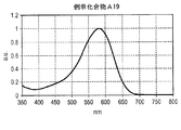
- FIG. 3 is a figure which shows the ultraviolet visible absorption spectrum of exemplary compound A19 shown below.
- the UV-visible absorption spectrum is measured in a diluted toluene solution and at room temperature.
- model V-560 (trade name) manufactured by JASCO is used.
- the exemplary compound A2 had a maximum absorption wavelength of 546 nm and a half-value width in the visible light region of 198 nm (400 nm to 598 nm) as shown in FIG.
- the maximum absorption wavelength was 582 nm and the half width in the visible light region was 112 nm, as shown in FIG.
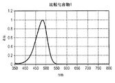
- Comparative compound 1 is compound 1-A disclosed in Patent Document 1
- Comparative compound 2 is compound 1-B disclosed in Patent Document 1.
- FIG. 4 is a diagram showing an ultraviolet-visible absorption spectrum of Comparative Compound 1.
- FIG. 5 is a view showing an ultraviolet-visible absorption spectrum of Comparative Compound 2.
- the measurement conditions of the ultraviolet-visible absorption spectrum are the same as those in the case of the exemplary compound A2 and the exemplary compound A19.
- the maximum absorption wavelength was 484 nm and the half-value width in the visible light region was 62 nm, as shown in FIG.
- the maximum absorption wavelength was 498 nm
- the half-value width in the visible light region was 76 nm, as shown in FIG.
- Comparative Compounds 1 and 2 have a narrow wavelength range of light absorbed by the compound itself, and in particular, there is almost no absorption in the red region (around 600 nm). Yes. For this reason, it is not suitable as a constituent material of an organic photoelectric conversion element.
- the compounds (Exemplary Compound A2, Exemplified Compound A19) corresponding to the compound of the general formula [1] have a wide absorption wavelength region of the compound itself, and the maximum absorption wavelength is shifted to the longer wavelength side.
- Comparative Compound 3 shown below in which the linking group contained in the compound is an anthracene-2,6-diyl group (condensed polycyclic aromatic hydrocarbon group). Comparative compound 3 is compound 1-C disclosed in Patent Document 1.
- Comparative Compound 3 was confirmed to be decomposed by oxidation during the synthesis, and could not be synthesized. This is considered because the comparative compound 3 has a reaction active site.
- acene a compound having a structure in which a plurality of benzene rings are linearly condensed.
- the structure becomes unstable as the number of condensed benzene rings increases (at least 3 or more).
- anthracene which is a typical compound of acene shown below, receives an electron donation from the benzene rings at both ends, so that the electron density of the central benzene ring is high. For this reason, anthracene is susceptible to an oxidation reaction in the central benzene ring. That is, anthracene has sites (active sites) unstable to oxidation at the 9th and 10th positions in the center.
- Comparative Compound 3 has an anthracene skeleton, which is an acene, as a partial structure. Further, in this anthracene skeleton, the substitution positions (9th and 10th positions) indicated by * in Table 1 are reactive active sites. For this reason, since the comparative compound 3 is a compound unstable to oxidation, it is not a suitable material as a constituent material of the organic photoelectric conversion element. On the other hand, the compounds corresponding to the compound represented by the general formula [1] (Exemplary Compound A2, Exemplified Compound A19) do not have a partial skeleton having a reaction active site, and thus are stable compounds against oxidation. is there.
- the compound of the general formula [1] is a compound having the properties (i) and (ii) above, it can perform photoelectric conversion in the entire visible light region as compared with the comparative compounds 1 to 3.
- the organic photoelectric conversion device having the compound of the general formula [1] has high stability of the device itself.
- a spin coat method is used as a method of forming the layer (1st organic compound layer 10) containing the compound of General formula [1]
- a spin coat method is used as a method of forming the layer (1st organic compound layer 10) containing the compound of General formula [1]
- vacuum deposition vacuum deposition method
- a compound having a lower molecular weight so that sublimation purification and film formation can be performed without excessive heating. Also, it is preferable to select a partial structure constituting the compound that does not have a reactive active substitution position, because the stability of the compound itself at a high temperature increases.
- Ar 1 and Ar 2 in the formula [1] when at least one of Ar 1 and Ar 2 in the formula [1] is an aromatic hydrocarbon group, a phenyl group and a naphthyl group are preferable because they have a relatively small molecular weight.
- Ar 1 and Ar 2 when at least one of Ar 1 and Ar 2 is a heteroaromatic ring group, a pyridyl group, a benzothienyl group, and a benzofuranyl group are preferable because they are relatively low molecular weight and highly stable substituents.
- the substituents of the formulas [2a] to [2c] are preferable because they are relatively low molecular weight and highly stable substituents.
- the organic photoelectric conversion element of the present invention whether or not the compound of the general formula [1] is present in the constituent members of the organic photoelectric conversion element such as the first organic compound layer 10 is included in the organic photoelectric conversion element.
- the layer can be verified by analyzing with TOF-SIMS or the like. Further, instead of the analysis by TOF-SIMS or the like, a method of extracting the constituent material of the organic photoelectric conversion element and analyzing it by IR, UV, NMR or the like may be employed.
- compounds having numbers beginning with A that is, compounds corresponding to Group A, have 6 carbon atoms in which Ar 1 and Ar 2 in formula [1] may have a substituent.
- the chemical stability of the compound itself is increased. Therefore, the compound corresponding to Group A is a compound having excellent thermal stability and sublimation properties.
- Exemplified Compounds A1 to A12 are such that Ar 3 in the formula [1] is a pyrenediyl group and Q in the formula [1] is any one of the general formulas [2a] to [2c] Therefore, the compound is particularly excellent in thermal stability and sublimation.
- the exemplified compounds A13 to A24 have Ar 3 in the formula [1] being a perylene diyl group and the substituent Q is any one of the general formulas [2a] to [2c], the longest absorption wavelength is particularly long. It is a compound excellent in wavelength conversion and sublimation.
- the exemplary compounds A3, A4, A15 and A16 have a methylene group or an ethylene group in which Ar 1 and Ar 2 , or Ar 2 and Ar 3 may have a single bond or an alkyl group (for example, a methyl group).
- a ring structure is formed by bonding via each other. Since the melting point of the compound itself is increased by the formation of this ring structure, the compound is excellent in thermal stability.
- a compound having a number beginning with B that is, a compound corresponding to group B is the number of carbon atoms in which either Ar 1 or Ar 2 in formula [1] may have a substituent. 3 to 15 heteroaromatic ring groups.
- the heteroaromatic ring has a nitrogen atom
- the electron withdrawing property of the nitrogen atom increases the oxidation potential of the compound itself (in other words, the oxidation potential becomes deeper), so that it is stable against oxidation.
- the heteroaromatic ring has a sulfur atom or an oxygen atom
- the sulfur atom or oxygen atom has many unshared electron pairs, so that the interaction between molecules is increased and the compound has an excellent carrier transport ability. That is, the compounds corresponding to Group B are particularly excellent compounds in terms of stability due to electronic effects and carrier transportability.
- the exemplary compounds B1 to B12 are particularly preferable because Ar 3 in the formula [1] is a pyrenediyl group and Q in the formula [1] is any one of the general formulas [2a] to [2c]. It is a compound with excellent thermal stability and sublimation properties.
- Exemplified compounds B13 to B24 are particularly maximal because Ar 3 in the formula [1] is a perylene diyl group and Q in the formula [1] is any one of the general formulas [2a] to [2c]. It is a compound that has a long absorption wavelength and excellent sublimation properties.
- the first organic compound layer 10 may be a layer made of only the compound of the general formula [1]. This is because the compound represented by the general formula [1] has a function of generating excitons by absorbing visible light and a function of generating and transporting charges, that is, holes and electrons, from the excitons. It is. In particular, the function of generating excitons by absorbing visible light is excellent.
- the first organic compound layer 10 may include other materials than the compound of the general formula [1].
- Other materials include a light-absorbing material that absorbs visible light and generates excitons, and a function that generates and transports charges, that is, holes and electrons, from excitons of the light-absorbing material.
- a photoelectric conversion induction material is mentioned.
- the first organic compound layer 10 includes a material (light absorption material, photoelectric conversion inducing material) other than the compound of the general formula [1]
- the light absorption material included in the first organic compound layer 10 may be one kind or two or more kinds.
- a photoelectric conversion part is a 1st organic compound which has a compound of General formula [1]
- a layered body in which the layer 10 and a layer having another material are stacked may be used.
- the photoelectric conversion part is comprised with the laminated body which laminates
- Photoelectric conversion-inducing materials other than the compound of general formula [1] include n-type organic semiconductors, specifically fullerene derivatives, naphthalene compounds such as NTCDI, perylene compounds such as PTCDI, phthalocyanine compounds such as SubPc, DCV3T, and the like. Examples include thiophene compounds.
- fullerene derivatives are preferable. Fullerene derivatives are particularly excellent in the function of generating and transporting charges (holes and electrons) from excitons among the n-type organic semiconductors described above, and also have the function of generating excitons by absorbing visible light. Because it is a material to prepare.
- One type of these photoelectric conversion inducing materials may be used, or two or more types may be used.
- Fullerene which is a skeleton that the fullerene derivatives have in common, is a generic name for closed-shell hollow clusters composed of only a large number of carbon atoms. Specific examples of the fullerene include C60 and higher-order fullerenes C70, C74, C76, and C78.
- a fullerene derivative is a compound in which a substituent such as an alkyl group, an aryl group, or a heterocyclic group is introduced into fullerene.
- fullerenes and fullerene derivatives may be collectively referred to as “fullerenes”.
- One of these compounds may be selected and used, or a plurality of types may be selected and used.
- Fullerenes contained in the first organic compound layer 10 can be used as an n-type organic semiconductor. Further, since the molecules of fullerene cause stacking between the fluoranthene skeletons, each molecule can be connected (oriented) in a certain direction in the first organic compound layer 10. Thereby, since an electron path is formed, the electron transport property is improved, and the high-speed response of the organic photoelectric conversion element is improved.
- the content of fullerenes contained in the first organic compound layer 10 is preferably 20% by volume or more and 80% by volume or less with respect to the entire first organic compound layer 10.
- fullerenes fullerene, fullerene derivative
- fullerene C60 fullerene C70, fullerene C76, fullerene C78, fullerene C80, fullerene C82, fullerene C84, fullerene C90, fullerene C96
- fullerene C240 fullerene 540, mixed fullerene, fullerene nanotubes, and fullerene derivatives shown below.
- the organic photoelectric conversion element of the present invention may have a substrate.
- the substrate include a silicon substrate, a glass substrate, and a flexible substrate.
- the constituent material of the hole collection electrode 13 is not particularly limited as long as it is a material having high conductivity and transparency.
- conductive metal oxides such as tin oxide (ATO, FTO) doped with antimony or fluorine, tin oxide, zinc oxide, indium oxide, indium tin oxide (ITO), zinc indium oxide, gold,
- Metal materials such as silver, chromium, nickel, titanium, tungsten and aluminum, and conductive compounds such as oxides and nitrides of these metal materials (for example, titanium nitride (TiN)), and these metals and conductive metal oxidation Examples thereof include a mixture or laminate with a material, an inorganic conductive material such as copper iodide and copper sulfide, an organic conductive material such as polyaniline, polythiophene and polypyrrole, and a laminate of these with ITO or titanium nitride.
- the constituent material of the hole collecting electrode 13 is particularly preferably a
- Electron Collection Electrode As a constituent material of the electron collection electrode 14, specifically, ITO, indium zinc oxide, SnO 2 , ATO (antimony-doped tin oxide), ZnO, AZO (Al-doped zinc oxide) , GZO (gallium-doped zinc oxide), TiO 2 , FTO (fluorine-doped tin oxide), and the like.
- the formation method of the two types of electrodes (13, 14) described above can be appropriately selected in consideration of suitability with the electrode material used for each. Specifically, it can be formed by a wet method such as a printing method or a coating method, a physical method such as a vacuum deposition method, a sputtering method, or an ion plating method, or a chemical method such as CVD or plasma CVD method.
- An electrode can be formed.
- the surface of the formed electrode (ITO electrode) may be subjected to UV-ozone treatment, plasma treatment, or the like.
- various film forming methods including a reactive sputtering method can be used.
- the formed electrode (TiN electrode) may be subjected to annealing treatment, UV-ozone treatment, plasma treatment, or the like.
- examples of the constituent material of the second organic compound layer 11 include organic compounds used as a hole transport material or a hole injection material. .
- the constituent material of the third organic compound layer 12 is a material having a high ionization potential, specifically, an electron transport material or an electron injection.
- the organic compound used as a material is mentioned. Since the first compound having a fullerene skeleton which is one of the constituent materials of the first organic compound layer 10 is a material having excellent electron transport properties as described above, the third organic compound layer It can be used as 12 constituent materials.
- the organic photoelectric conversion device of the present invention can be an organic photoelectric conversion device corresponding to light of different wavelengths by appropriately setting the constituent material of the first organic compound layer.
- the “wavelength” is the wavelength of light received by a predetermined organic photoelectric conversion element.
- FIG. An organic photoelectric conversion device is obtained that does not require the color filter shown.
- the plurality of types of organic photoelectric conversion elements included in the organic photoelectric conversion device at least one type of organic photoelectric conversion element is the organic photoelectric conversion element according to the present invention.
- the organic photoelectric conversion element according to the present invention can be used as a constituent member of an optical area sensor by being two-dimensionally arranged in the in-plane direction.
- the optical area sensor has a plurality of organic photoelectric conversion elements, and a plurality of organic photoelectric conversion elements are arranged in the front direction and the column direction, respectively.
- the organic photoelectric conversion element according to the present invention can be used as a constituent member of an imaging element.
- the imaging element has a plurality of organic photoelectric conversion elements each serving as a light receiving pixel, and a transistor connected to each organic photoelectric conversion element.
- a transistor here is a transistor which reads the electric charge generated from the organic photoelectric conversion element.
- Information based on the electric charge read by the transistor is transmitted to a sensor unit connected to the image sensor. Examples of the sensor unit include a CMOS sensor and a CCD sensor. An image can be obtained by collecting the information acquired by each light receiving pixel in the sensor unit.
- the image sensor may have, for example, an optical filter such as a color filter so as to correspond to each light receiving pixel.
- an optical filter such as a color filter so as to correspond to each light receiving pixel.
- the organic photoelectric conversion element supports light of a specific wavelength, it is preferable to have a color filter that transmits light in a wavelength region that can be handled by the organic photoelectric conversion element.
- One color filter may be provided for each light receiving pixel, or one color filter may be provided for a plurality of light receiving pixels.
- the optical filter included in the image pickup device is not limited to a color filter. Besides, a low-pass filter that transmits a wavelength equal to or greater than the wavelength of infrared light, a UV cut filter that transmits a wavelength equal to or smaller than the wavelength of ultraviolet light, and a long-pass filter Can be used.
- the imaging device may have an optical member such as a microlens so as to correspond to each light receiving pixel, for example.
- the microlens included in the image sensor is a lens that condenses light from the outside onto a photoelectric conversion unit included in the organic photoelectric conversion element included in the image sensor.
- One microlens may be provided for each light receiving pixel, or one microlens may be provided for a plurality of light receiving pixels. In the case where a plurality of light receiving pixels are provided, it is preferable that one microlens is provided for a plurality (two or more predetermined numbers) of light receiving pixels.
- the organic photoelectric conversion element according to the present invention can be used in an imaging apparatus.
- the imaging apparatus includes an imaging optical system having a plurality of lenses, and an imaging element that receives light that has passed through the imaging optical system.
- the imaging device may be an imaging device having a joint portion that can be joined to the imaging optical system and an imaging element. More specifically, the imaging device here refers to a digital camera or a digital still camera.
- the imaging device may further include a receiving unit that receives an external signal. The signal received by the receiving unit is a signal that controls at least one of the imaging range of the imaging apparatus, the start of imaging, and the end of imaging.
- the imaging device may further include a transmission unit that transmits an image acquired by imaging to the outside. As described above, the imaging device can be used as a network camera by including the reception unit and the transmission unit.
- the obtained exemplary compound A2 was identified by the following method.
- MALDI-TOF-MS Microx-Assisted Ionization-Time-of-Flight Mass Spectrometry
- Autoflex LRF (trade name) manufactured by Bruker)
- m / z 637.51
- C 46 H 39 NO 2 637.81
- ⁇ max the maximum absorption wavelength
- Synthesis Example 1 (1) cross-coupling reaction with arylamine
- the stability of the compound was decreased, and a decrease in purity was confirmed during column purification.
- Synthesis Example 1 (2) formylation reaction using n-butyllithium
- Comparative Compound 3 could not be obtained, and a device having Comparative Compound 3 was not produced.
- Example 1 Production of photoelectric conversion element On a substrate, a hole collection electrode, an electron blocking layer (second organic compound layer), a photoelectric conversion part (first organic compound layer), a hole blocking layer (first Three organic compound layers) and a photoelectric conversion element in which an electron collecting electrode is sequentially formed were produced by the method described below.
- an indium zinc oxide film was formed on a Si substrate, and then a hole collecting electrode was formed by performing a patterning process so as to have a desired shape. At this time, the thickness of the hole collecting electrode was set to 100 nm. Thus, the board
- an organic compound layer and an electrode layer shown in Table 2 below were continuously formed on the substrate with electrodes.
- the electrode area of the opposing electrode was set to 3 mm 2 .
- the following compound Y2 was used as the constituent material Z1 of an electron blocking layer.
- Example 1 Production of Photoelectric Conversion Element
- the constituent material Z1 of the second organic compound layer and the constituent materials Z2 and Z3 of the first organic compound layer are as follows. As shown in Table 2, an organic photoelectric conversion element was produced in the same manner as in Example 1 except that the materials were appropriately changed.
- the structures of the compound Y1 used in Examples 5, 10 and 12, and the compound Y3 used in Examples 3, 4 and 9 are shown below.
- Quantum yield External quantum efficiency was measured about the obtained organic photoelectric conversion element.
- the external quantum efficiency is a single color with an intensity of 50 ⁇ W / cm 2 at wavelengths of 450 nm, 500 nm, and 600 nm in a state where a voltage of 5 V is applied between the hole collecting electrode and the electron collecting electrode. It was calculated by measuring the density of the photocurrent that flows when the device was irradiated with light. The photocurrent density was determined by subtracting the dark current density during light shielding from the current density during light irradiation.
- the organic photoelectric conversion device according to the present invention has high external quantum efficiency in the blue region (wavelength around 450 nm), the green region (wavelength near 500 nm), and the red region (wavelength near 600 nm). It was found that photoelectric conversion can be performed efficiently over the entire region. On the other hand, in the organic photoelectric conversion element of the comparative example, it turned out that the photoelectric conversion efficiency in wavelength 600nm is small. This is because the half-value width of the absorption spectrum of the light-absorbing material included in the organic photoelectric conversion element according to the present invention is wide and the absorption is large even in the vicinity of a wavelength of 600 nm.
- organic photoelectric conversion element 10: first organic compound layer, 11: second organic compound layer (electron blocking layer), 12: third organic compound layer (hole blocking layer), 13: hole trapping Collector electrode, 14: electron collector electrode, 15: readout circuit, 16: inorganic protective layer, 17: color filter, 18: microlens
Landscapes
- Chemical & Material Sciences (AREA)
- Organic Chemistry (AREA)
- Engineering & Computer Science (AREA)
- Materials Engineering (AREA)
- Physics & Mathematics (AREA)
- Spectroscopy & Molecular Physics (AREA)
- Multimedia (AREA)
- Signal Processing (AREA)
- Electromagnetism (AREA)
- Nanotechnology (AREA)
- Light Receiving Elements (AREA)
- Photovoltaic Devices (AREA)
- Solid State Image Pick-Up Elements (AREA)
- Transforming Light Signals Into Electric Signals (AREA)
Abstract
電子捕集電極14と、正孔捕集電極13と、電子捕集電極14と正孔捕集電極13との間に配置されている光電変換部と、を有する有機光電変換素子であって、前記光電変換部が、少なくとも第一の有機化合物層10を有し、第一の有機化合物層10が、下記一般式[1]により表される化合物を有する有機光電変換素子1。
Description
本発明は、有機光電変換素子、並びにこれを用いた二次元センサ、画像センサ及び撮像装置に関する。
カメラ等に含まれる撮像素子として、平面型受光素子が広く用いられている。この平面型受光素子は、フォトダイオードを有する画素を2次元的に複数配列させてなる素子である。また、この平面型受光素子が光を受けると、画素の光電変換により発生した信号(電荷)がCCD回路やCMOS回路を用いて転送され、受光素子内又は他の部材においてこの信号の読み出しが行なわれる。また、従来の撮像素子に備えられているフォトダイオードとしては、シリコン等の半導体基板中に光電変換部を形成したものが知られている。
一方で、光電変換部に有機化合物を用いた素子、即ち、有機光電変換素子の開発が進んでいる。かかる有機光電変換素子によれば、有機化合物が有する高い吸光係数や柔軟性から、撮像素子の高感度化、薄型・軽量化、フレキシブル化等が可能であると期待されている。しかしながら、一般に、有機化合物が吸収する光の波長領域は狭く、また当該有機化合物が吸収する光の波長領域は、当該有機化合物の分子サイズに依存するところが多いため、低分子量で長波長の領域に吸収スペクトルを有する化合物の発見、生成の報告は少なかった。さらに、有機光電変換素子が光電変換可能な光の波長領域は、光電変換部の構成材料となる有機化合物がどの波長領域の光を吸収するかに依存するため、可視光領域の光を全て吸収し得る有機化合物の提供が望まれている。特許文献1には、下記化合物1-A~1-Cのいずれかを有する有機光電変換素子が開示されている。
一方で、光電変換部に有機化合物を用いた素子、即ち、有機光電変換素子の開発が進んでいる。かかる有機光電変換素子によれば、有機化合物が有する高い吸光係数や柔軟性から、撮像素子の高感度化、薄型・軽量化、フレキシブル化等が可能であると期待されている。しかしながら、一般に、有機化合物が吸収する光の波長領域は狭く、また当該有機化合物が吸収する光の波長領域は、当該有機化合物の分子サイズに依存するところが多いため、低分子量で長波長の領域に吸収スペクトルを有する化合物の発見、生成の報告は少なかった。さらに、有機光電変換素子が光電変換可能な光の波長領域は、光電変換部の構成材料となる有機化合物がどの波長領域の光を吸収するかに依存するため、可視光領域の光を全て吸収し得る有機化合物の提供が望まれている。特許文献1には、下記化合物1-A~1-Cのいずれかを有する有機光電変換素子が開示されている。

特許文献1に開示されている化合物1-A及び1-Bの吸収スペクトルは、いずれもその極大吸収波長が青(波長450nm付近)から緑(波長500nm付近)の領域にあり、またその吸収スペクトルの半値幅は狭かった。そのため、これらの化合物を用いた有機光電変換素子は、特に、赤領域(波長600nm付近)での光電変換効率が低かった。また特許文献1に開示されている化合物1-Cは化合物自体の安定性が低いため、この化合物1-Cを有機光電変換素子の構成材料として用いると、素子の安定性を損ねるという問題があった。
本発明は、上述した課題を解決するためになされたものであり、その目的は、可視光領域の全域での光電変換効率が良好であり、かつ素子自体の安定性が高い有機光電変換素子を提供することにある。
本発明は、上述した課題を解決するためになされたものであり、その目的は、可視光領域の全域での光電変換効率が良好であり、かつ素子自体の安定性が高い有機光電変換素子を提供することにある。
本発明に係る有機光電変換素子は、電子捕集電極と、正孔捕集電極と、前記電子捕集電極と前記正孔捕集電極との間に配置されている光電変換部と、を有する有機光電変換素子であって、
前記光電変換部が、少なくとも第一の有機化合物層を有し、
前記第一の有機化合物層が、下記一般式[1]で表わされる化合物を有する。
前記光電変換部が、少なくとも第一の有機化合物層を有し、
前記第一の有機化合物層が、下記一般式[1]で表わされる化合物を有する。


本発明に係る有機光電変換素子は、光電変換部に、吸収スペクトルの半値幅が広く、かつ構造自体の安定性が高い有機化合物が含まれている。このため、本発明によれば、可視光領域の全域での光電変換効率が良好であり、かつ素子自体の安定性が高い有機光電変換素子を提供することができる。
本発明は、電子捕集電極と、正孔捕集電極と、前記電子捕集電極と前記正孔捕集電極との間に配置されている光電変換部と、を有する有機光電変換素子に関する。本発明において、光電変換部は、少なくとも第一の有機化合物層を有し、この第一の有機化合物層は、下記一般式[1]により表される化合物を有している。

なお、一般式[1]により表される化合物の詳細については、後述する。
1.有機光電変換素子
(1)有機光電変換素子の実施形態
以下、図面を参照しながら、本発明に係る有機光電変換素子の実施形態について説明する。図1は、本発明の有機光電変換素子における実施形態の一例を示す断面模式図である。図1に示す有機光電変換素子1は、正孔捕集電極13と、電子捕集電極14と、正孔捕集電極13と電子捕集電極14との間に配置されている第一の有機化合物層10と、を有する。
(1)有機光電変換素子の実施形態
以下、図面を参照しながら、本発明に係る有機光電変換素子の実施形態について説明する。図1は、本発明の有機光電変換素子における実施形態の一例を示す断面模式図である。図1に示す有機光電変換素子1は、正孔捕集電極13と、電子捕集電極14と、正孔捕集電極13と電子捕集電極14との間に配置されている第一の有機化合物層10と、を有する。
図1に示す有機光電変換素子1を構成する正孔捕集電極13は、第一の有機化合物層10で発生した電荷の一つである正孔を捕集する電極である。
図1に示す有機光電変換素子1を構成する電子捕集電極14は、後述するように第一の有機化合物層10で発生した電荷の一つである電子を捕集する電極である。図1に示す有機光電変換素子1において、電子捕集電極14は、正孔捕集電極13よりも画素回路(例えば、読み出し回路15)に近い側に配置されるが、本発明においては、正孔捕集電極13の方を電子捕集電極14よりも画素回路に近い側に配置してもよい。
図1に示す有機光電変換素子1において、第一の有機化合物層10は、層内に、光を受けることで励起する化合物を有している。また第一の有機化合物層10は、当該化合物の分子を光で励起させた後で生じる電荷、即ち、電子及び正孔を電子捕集電極14、正孔補集電極13へそれぞれ運搬する役割も果たしている。第一の有機化合物層10には、後述するように光を電荷に変換する有機化合物が含まれるため、第一の有機化合物層10は光電変換層又は光電変換部を構成する層である。ただし、本発明において、有機光電変換素子を構成する光電変換部は、第一の有機化合物層10のみに限定されるものではない。
第一の有機化合物層10は、p型の有機半導体又はn型の有機半導体を含む層であることが好ましい。また、第一の有機化合物層10は、少なくともその一部がp型の有機半導体とn型の有機半導体とを含むバルクへテロ層(混合層)であることがより好ましい。第一の有機化合物層10の少なくとも一部が、p型の有機半導体とn型の有機半導体とを含むバルクへテロ層であることにより、素子の光電変換効率(感度)をより向上させることができる。また第一の有機化合物層10を形成する際に、p型の有機半導体とn型の有機半導体とを適当な混合比率で含ませることにより、第一の有機化合物層10内における電子移動度及び正孔移動度を高くすることができ、有機光電変換素子の光応答速度をより高速にすることができる。
本発明において、第一の有機化合物層10は、一層で構成されるのが好ましいが、複数の層で構成されていてもよい。また本発明において、第一の有機化合物層10は、非発光であることが好ましい。ここでいう非発光とは、可視光領域(波長400nm~730nm)において発光量子効率が1%以下であること、好ましくは0.5%以下であること、より好ましくは0.1%以下の層であることをいう。光電変換部となる第一の有機化合物層10において、発光量子効率が1%を超えると、本発明の有機光電変換素子をセンサや撮像素子の構成部材として適用した場合にセンシング性能又は撮像性能に影響を与えるため、好ましくない。なお、第一の有機化合物層10に含まれ得る化合物の詳細については、後述する。
図1に示す有機光電変換素子1において、正孔捕集電極13と第一の有機化合物層10との間には、第二の有機化合物層11が設けられている。本発明において、第二の有機化合物層11は、一層で構成されていてもよいし、複数の層で構成されていてもよい。また第二の有機化合物層11は、複数種の材料を有するバルクへテロ層(混合層)であってもよい。図1に示す有機光電変換素子1において、第二の有機化合物層11は、第一の有機化合物層10から移動した正孔を正孔捕集電極13へ輸送する役割を果たす。また第二の有機化合物層11は、正孔捕集電極13から光電変換部へ電子が移動するのを抑制する。つまり、第二の有機化合物層11は、正孔輸送層又は電子ブロッキング層として機能する。図1に示すように、第二の有機化合物層11は、正孔捕集電極13と接していることが好ましい。
なお、本発明においては、図1に示すように、電子捕集電極14と第一の有機化合物層10との間に第三の有機化合物層12を設けてもよい。第三の有機化合物層12は、第一の有機化合物層10と電子捕集電極14との間に設けられる層である。図1に示す有機光電変換素子1において、第三の有機化合物層12は、第一の有機化合物層10から移動した電子を電子捕集電極14へ輸送する役割を果たす。また第三の有機化合物層12は、電子捕集電極14から第一の有機化合物層10へ正孔が流れ込むのを抑制する層(正孔ブロッキング層)であるため、イオン化ポテンシャルが高い層であることが好ましい。図1に示すように、第三の有機化合物層12を設ける場合、第三の有機化合物層12は、一層で構成されていてもよいし、複数の層で構成されていてもよい。また第三の有機化合物層12は、複数種の材料を有するバルクへテロ層(混合層)であってもよい。また本発明において、第三の有機化合物層12は、図1に示すように、第一の有機化合物層10と電子捕集電極14との間に配置されている。このとき第三の有機化合物層12は、電子捕集電極14と接していることが好ましい。
本発明において、電子捕集電極14と正孔捕集電極13との間に配置される層は、上述した三種類の層(第一の有機化合物層10、第二の有機化合物層11、第三の有機化合物層12)に限定されるものではない。有機化合物層と正孔捕集電極13との間、又は有機化合物層と電子捕集電極14の間に介在層をさらに設けることができる。この介在層は、発生した電荷を電極に注入する際の電荷の注入効率を向上させる、もしくは電荷を印加した際に電荷が有機化合物層に注入されるのを阻止する目的で設けられる。この介在層を設ける場合、この介在層は有機化合物を有する有機化合物層であってもよいし、無機化合物を有する無機化合物層であってもよい。
図1に示す有機光電変換素子1において、電子捕集電極14は、読み出し回路15と接続されている。ただし、読み出し回路15は、正孔捕集電極13と接続されていてもよい。読み出し回路15は、第一の有機化合物層10において発生した電荷に基づく情報を読み出し、例えば、後段に配された信号処理回路(不図示)に当該情報を伝える役割を果たす。読み出し回路15には、例えば、有機光電変換素子1において生じた電荷に基づく信号を出力するトランジスタが含まれている。
図1に示す有機光電変換素子1において、正孔捕集電極13の上には無機保護層16が配置されている。無機保護層16は、電子捕集電極14と、第三の有機化合物層12と、第一の有機化合物層10と、第二の有機化合物層11と、正孔捕集電極13と、がこの順で積層されてなる部材を保護するための層である。無機保護層16の構成材料としては、酸化珪素、窒化珪素、酸化アルミニウム等が挙げられ、公知の成膜方法により層を形成することができる。
図1に示す有機光電変換素子1において、無機保護層16の上には、カラーフィルタ17が配置されている。カラーフィルタ17としては、例えば、可視光のうち赤色の光を透過するカラーフィルタ等が挙げられる。また本発明において、カラーフィルタ17の設け方としては、有機光電変換素子一個あたり一つであってもよいし、有機光電変換素子複数個あたり一つであってもよい。さらにカラーフィルタ17を配列する際には、例えば、隣接する有機光電変換素子とで、ベイヤー配列を形成してよい。
図1に示す有機光電変換素子1において、カラーフィルタ17の上には、マイクロレンズ18等の光学部材が配置されている。マイクロレンズ18は、入射した光を光電変換部である第一の有機化合物層10に集光する役割を果たす。また本発明において、マイクロレンズ18の設け方としては、有機光電変換素子一個あたり一つであってもよいし、有機光電変換素子複数個あたり一つであってもよい。本発明においては、有機光電変換素子一個あたり一つのマイクロレンズ18を設けることが好ましい。
本発明に係る有機光電変換素子を用いて光電変換を行う場合は、正孔捕集電極13と電子捕集電極14との間に電圧を印加することが好ましい。ここで両電極間に印加する電圧は、有機化合物層(10、11、12)の総膜厚にもよるが、好ましくは、1V以上15V以下である。より好ましくは、2V以上10V以下である。
(2)第一の有機化合物層
次に、本発明に係る有機光電変換素子の光電変換部に含まれる第一の有機化合物層について、層に含まれる構成材料と共に詳細に説明する。
次に、本発明に係る有機光電変換素子の光電変換部に含まれる第一の有機化合物層について、層に含まれる構成材料と共に詳細に説明する。
(2-1)一般式[1]の化合物
まず、第一の有機化合物層10に構成材料の一つとして含まれる下記一般式[1]の化合物について説明する。
まず、第一の有機化合物層10に構成材料の一つとして含まれる下記一般式[1]の化合物について説明する。

式[1]において、Ar1及びAr2は、それぞれ独立的に、炭素原子数1~8のアルキル基、炭素原子数6~18の芳香族炭化水素基又は炭素原子数3~15の複素芳香環基を表す。
Ar1及びAr2で表されるアルキル基として、メチル基、エチル基、n-プロピル基、iso-プロピル基、n-ブチル基、iso-ブチル基、sec-ブチル基、tert-ブチル基、n-ペンチル基、n-ヘキシル基、シクロヘキシル基、n-ヘプチル基、n-オクチル基が挙げられる。好ましくは、メチル基及びtert-ブチル基である。
Ar1及びAr2で表される芳香族炭化水素基として、フェニル基、ナフチル基、フェナントリル基、フルオレニル基等が挙げられる。昇華性の観点から、比較的分子量の小さい置換基が好ましく、具体的には、フェニル基及びナフチル基が好ましい。
Ar1及びAr2で表される複素芳香環基としては、ピリジル基、ピラジニル基、ピリミジニル基、キノリル基、イソキノリル基、チエニル基、フラニル基、ベンゾチエニル基、ベンゾフラニル基、トリアジニル基等が挙げられる。昇華性及び安定性の観点から、比較的分子量が小さく、安定性の高い置換基が好ましく、具体的には、ピリジル基、ベンゾチエニル基及びベンゾフラニル基が好ましい。
なお、Ar1及びAr2は、フッ素原子、塩素原子、臭素原子、ヨウ素原子等のハロゲン原子、シアノ基、メチル基、エチル基、n-プロピル基、iso-プロピル基、n-ブチル基、iso-ブチル基、sec-ブチル基、tert-ブチル基、n-ペンチル基、n-ヘキシル基、シクロヘキシル基等の炭素原子数1~6のアルキル基、フェニル基、トリル基、キシリル基、メシチル基及びクメニル基から選択される置換基をさらに有してもよい。Ar1及びAr2のいずれかが炭素原子数1~6のアルキル基をさらに有する場合、当該アルキル基として、好ましいものはメチル基及びtert-ブチル基である。Ar1及びAr2のいずれかがハロゲン原子をさらに有する場合、当該ハロゲン原子として好ましいものはフッ素原子である。
また、Ar1及びAr2が、炭素原子数6~18の芳香族炭化水素基又は炭素原子数3~15の複素芳香環基である場合、Ar1とAr2とが、単結合、メチル基等のアルキル基を有してもよいメチレン基又はエチレン基のいずれかを介して互いに結合して、環構造、例えば、下記に示される環構造を形成してもよい。

式[1]において、Ar3は、4個又は5個の六員環が縮合することにより構成される縮合多環芳香族炭化水素基を表す。ただし、アセン基に該当する置換基、具体的には、テトラセンジイル基及びペンタセンジイル基は除かれる。本発明において、Ar3で表される置換基からアセン基が除かれる理由については後述する。
Ar3で表される縮合多環芳香族炭化水素基として、好ましくは、ピレンジイル基、ベンゾピレンジイル基、トリフェニレンジイル基、ペリレンジイル基及びクリセンジイル基から選択される置換基である。化合物自体の昇華性を考慮すると、Ar3となる置換基として、より好ましいものは、比較的分子量の小さいピレンジイル基である。一方、化合物自体の吸収スペクトルの長波長化を考慮すると、Ar3となる置換基として、より好ましいものはペリレンジイル基である。他方、化合物自体の遷移(双極子)モーメントを考慮すると、Ar3となる置換基として、より好ましいものは、ピレン-1,6-ジイル基又はペリレン-3,10-ジイル基である。これら置換基は、ピレンジイル基やペリレンジイル基の中でも電子が遷移しやすく吸収係数が向上すると考えられる置換基だからである。
なお、Ar3は、フッ素原子、シアノ基、メチル基又はtert-ブチル基をさらに有していてもよい。
また、Ar2が、炭素原子数6~18の芳香族炭化水素基又は炭素原子数3~15の複素芳香環基である場合、Ar2とAr3とが、単結合、メチル基等のアルキル基を有してもよいメチレン基又はエチレン基のいずれかを介して互いに結合して環構造、例えば、下記に示される環構造を形成していてもよい。

式[1]において、Qは、下記一般式[2a]~[2e]により表される置換基群から選ばれる置換基である。昇華性及び安定性を考慮すると、式[2a]~[2e]により表される置換基群のうち、好ましいものは、比較的分子量が小さく、かつ安定性の高い置換基である式[2a]~[2c]により表される置換基群である。より好ましくは、[2a]又は[2c]である。

式[2a]~[2e]において、R1~R27は、それぞれ水素原子、フッ素原子、炭素原子数1~4のアルキル基及びシアノ基から選択される置換基である。
R1~R27で表されるアルキル基としては、メチル基、エチル基、n-プロピル基、iso-プロピル基、n-ブチル基、iso-ブチル基、sec-ブチル基、tert-ブチル基等が挙げられるが、これら置換基の中でも、好ましくは、メチル基又はtert-ブチル基である。
式[2a]~[2e]において、*は、Ar3との結合手を表す。
(一般式[1]の化合物の合成方法)
次に、一般式[1]の化合物の合成方法について説明する。一般式[1]の化合物は、例えば、下記式[3]の合成スキームに従って合成することができる。
次に、一般式[1]の化合物の合成方法について説明する。一般式[1]の化合物は、例えば、下記式[3]の合成スキームに従って合成することができる。

式[3]の合成スキームは、下記[3a]~[3c]の反応をこの順番で行う合成スキームである。
[3a]Pd触媒を用いて、アリールジハライドとアミンとを1対1でクロスカップリングさせる反応
[3b]n-ブチルリチウムを用いて、ハライドをホルミル(ケトン)化させる反応
[3c]クネーフェナーゲル縮合
[3a]Pd触媒を用いて、アリールジハライドとアミンとを1対1でクロスカップリングさせる反応
[3b]n-ブチルリチウムを用いて、ハライドをホルミル(ケトン)化させる反応
[3c]クネーフェナーゲル縮合
また、式[1]中のAr1及びAr2が、又はAr2及びAr3が、単結合、(アルキル基を有してもよい)メチレン基又はエチレン基を介して結合することによって環構造を形成する場合、例えば、下記式[4]の合成スキームに従って合成することができる。

式[4]の合成スキームは、下記[4a]~[4f]の反応をこの順番で行う合成スキームである。
[4a]Pd触媒を用いて、アリールハライドとアミンとを1対1でクロスカップリングさせる反応
[4b]Heck反応による環構造の形成
[4c]Pd触媒を用いて、アリールハライドと上記[4b]で形成された環構造を有するアミンとをクロスカップリングさせる反応
[4d]Ar3となる置換基([4b]にて形成された環構造に含まれている場合を含む)を対象としたBr化反応
[4e]n-ブチルリチウムを用いて、ハライドをホルミル(ケトン)化させる反応
[4f]クネーフェナーゲル縮合
なお、式[4]において、上記[4a]で用いられるアリールハライドが、Ar1-Brである場合、Ar1及びAr2が、単結合、(アルキル基を有してもよい)メチレン基又はエチレン基を介して結合されてなる環構造を有する化合物が得られる。
(一般式[1]の化合物の性質)
一般式[1]の化合物は、電子供与性の高い(ヘテロ)アリールアミン部位と、電子受容性の高い置換基とが、2価の縮合多環芳香族炭化水素基(Ar3)を介して連結している構造である。一般式[1]の化合物では、電子供与性の高い部位と、電子受容性の高い部位とを連結する置換基(連結基)は、比較的大きな縮合多環芳香族炭化水素基である。これにより、一般式[1]の化合物は、下記(i)及び(ii)の性質を有する。
(i)吸収スペクトルの半値幅(吸収の極大に対する相対吸光度が0.5以上となる波長領域の幅)が広く、吸収の極大が長波長領域に存在する。このため、可視光領域の全域に吸収領域を有する。
(ii)構造上に反応活性部位がなく、化合物自体の安定性が高い。
ここで、一般式[1]の化合物に該当する化合物の紫外可視吸収スペクトルの測定を行い、吸収スペクトルの概形、特に、吸収スペクトルの半値幅及び吸収の極大の位置(極大吸収波長)について検証する。図2は、下記に示される例示化合物A2の紫外可視吸収スペクトルを示す図である。また図3は、下記に示される例示化合物A19の紫外可視吸収スペクトルを示す図である。

なお、紫外可視吸収スペクトルの測定は、希釈トルエン溶液中で、かつ室温の条件下で行っている。また、測定装置としては、JASCO社製のモデルV-560(商品名)が用いられている。測定の結果、例示化合物A2においては、図2より、極大吸収波長が546nmであり、可視光領域における半値幅が198nm(400nm~598nm)であった。また例示化合物A19においては、図3より、極大吸収波長が582nmであり、可視光領域における半値幅が112nmであった。
なお、発明者らは、下記に示される比較化合物1及び2の紫外可視吸収スペクトルも測定している。なお、比較化合物1は、特許文献1に開示されている化合物1-Aであり、また比較化合物2は、特許文献1に開示されている化合物1-Bである。

図4は、比較化合物1の紫外可視吸収スペクトルを示す図である。また図5は、比較化合物2の紫外可視吸収スペクトルを示す図である。なお、紫外可視吸収スペクトルの測定条件は、例示化合物A2及び例示化合物A19の場合と同様である。測定の結果、比較化合物1においては、図4より、極大吸収波長は484nmであり、可視光領域における半値幅は62nmであった。また比較化合物2においては、図5より、極大吸収波長は498nmであり、可視光領域における半値幅は76nmであった。
各化合物の紫外可視吸収スペクトルの測定結果から、比較化合物1及び2は、化合物自体が吸収する光の波長領域が狭く、特に、赤領域(600nm付近)においては吸収がほぼ無いことが示されている。このため、有機光電変換素子の構成材料としては適さない。一方、一般式[1]の化合物に該当する化合物(例示化合物A2、例示化合物A19)は、化合物自体の吸収波長領域が広く、かつ極大吸収波長が長波長側にシフトしている。
これについては、以下のように考察される。つまり、一般式[1]の化合物では、電子供与性部位と電子受容性部位とが、比較的大きな縮合多環芳香族炭化水素基を介して連結されている。このため、電子供与性部位と電子受容性部位との間での、CT(Charge-Transfer)遷移に伴う吸収と、これら部位を連結する縮合多環芳香族炭化水素基のπ-π*遷移に伴う吸収と、が混在していると考えられる。ここで、極大吸収波長の長波長側へのシフトは、共役長が長い連結基である縮合多環芳香族炭化水素基を介してのCT遷移によるものであると考えられる。また吸収スペクトルの広域化(半値幅の拡張)は、電子供与性部位と電子受容性部位とを連結する縮合多環芳香族炭化水素基のπ-π*遷移によるものであると考えられる。
次に、一般式[1]の化合物が、反応活性部位がなく、化合物自体の安定性が高いことについて説明する。これまでの説明から、一般式[1]の化合物自体の安定性については、電子供与性部位と電子受容性部位とを連結する縮合多環芳香族炭化水素基の大きさ、及び化合物の吸収スペクトルに関係があると考えられる。そこで、化合物中に含まれる連結基がアントラセン-2,6-ジイル基(縮合多環芳香族炭化水素基)である下記に示される比較化合物3の合成を試みた。なお、比較化合物3は、特許文献1に開示されている化合物1-Cである。

しかしながら、比較化合物3は、合成途中において酸化により分解することが確認され、合成することができなかった。これは、比較化合物3が反応活性部位を有しているためと考えられる。
ところで、縮合多環芳香族炭化水素のうち、複数のベンゼン環が直線状に縮合した構造をもつ化合物をアセンと呼ぶ。アセン化合物の特徴の一つとして、縮合するベンゼン環の数が増加する(少なくとも3以上になる)につれて不安定な構造となることが知られている。
例えば、下記に示すアセンの代表的な化合物であるアントラセンは、両端のベンゼン環による電子供与を受けるため、中央のベンゼン環の電子密度が高い。このため、アントラセンは、中央のベンゼン環において酸化反応を受けやすい。即ち、アントラセンは、中央の9位及び10位の位置に、酸化に対して不安定な部位(活性部位)を有する。

ここで、例示化合物A2及びA19、並びに比較化合物3の構造を下記表1に示す。

表1に示すように、比較化合物3は、アセン類であるアントラセン骨格を部分構造として有している。またこのアントラセン骨格は、表1中の★で示した置換位置(9位、10位)が反応活性部位となる。このため比較化合物3は、酸化に対して不安定な化合物であるため、有機光電変換素子の構成材としては適さない材料である。一方で、一般式[1]で表される化合物に該当する化合物(例示化合物A2、例示化合物A19)は、反応活性部位を有する部分骨格を有していないため、酸化に対して安定な化合物である。
よって、一般式[1]の化合物は、上記(i)及び(ii)の性質を有する化合物であるため、比較化合物1~3と比較して、可視光領域の全域における光電変換が可能であり、一般式[1]の化合物を有する有機光電変換素子は素子自体の安定性が高くなる。
また一般式[1]の化合物を、有機光電変換素子の構成材料として用いる場合、一般式[1]の化合物を含む層(第一の有機化合物層10)を形成する方法としては、スピンコート法を採用してもよいが、真空下における蒸着(真空蒸着法)を利用するのが好ましい。真空蒸着法を利用すると、高純度な薄膜が形成できるからである。このように真空蒸着法を利用して第一の有機化合物層を形成する場合、一般に、層の構成材料となる有機化合物の分子量が大きいほど高温が必要とされる。そして、必要とされる温度があまりにも高いと、構成材料となる有機化合物の熱分解等が起こり易い。従って、過度に加熱することなく昇華精製や成膜を行うことができるように、化合物の分子量がより小さいものを選択することが好ましい。また化合物を構成する部分構造として、反応活性な置換位置を有さないものを選択することは、高温下における化合物自体の安定性が高くなるので、好ましい。
例えば、式[1]中の、Ar1及びAr2の少なくともいずれかが芳香族炭化水素基である場合、フェニル基及びナフチル基は比較的分子量が小さい置換基であるので、好ましい。またAr1及びAr2の少なくともいずれかがが複素芳香環基である場合、ピリジル基、ベンゾチエニル基及びベンゾフラニル基は、比較的分子量が小さく、安定性の高い置換基であるので、好ましい。さらに、式[1]中のQに該当する置換基のうち、式[2a]~[2c]の置換基は、比較的分子量が小さく、安定性の高い置換基であるので、好ましい。
本発明の有機光電変換素子において、第一の有機化合物層10等の有機光電変換素子の構成部材中に一般式[1]の化合物が存在するか否かについては、有機光電変換素子に含まれる層についてTOF-SIMS等による分析をすることで検証することができる。またTOF-SIMS等による分析に代えて、有機光電変換素子の構成材料を抽出し、IR、UV、NMR等により分析する方法を採用してもよい。
(一般式[1]の化合物の具体例)
以下、一般式[1]の化合物の具体例を示す。ただし、本発明において、一般式[1]の化合物は、これら具体例に限定されるものではない。
以下、一般式[1]の化合物の具体例を示す。ただし、本発明において、一般式[1]の化合物は、これら具体例に限定されるものではない。


上に例示した化合物のうち、Aで始まる番号を有する化合物、すなわちA群に該当する化合物は、式[1]中のAr1及びAr2が、置換基を有してもよい炭素原子数6~18の芳香族炭化水素基、又は置換基を有してもよい炭素原子数1~8のアルキル基である。これら置換基のいずれかを有することにより、化合物自体の化学的安定性が高くなるため、A群に該当する化合物は、熱安定性や昇華性に優れる化合物である。
これらの化合物のうち、例示化合物A1~A12は、式[1]中のAr3がピレンジイル基であって、式[1]中のQが一般式[2a]~[2c]のいずれかであるため、特に熱安定性及び昇華性に優れる化合物である。また、例示化合物A13~A24は、式[1]中のAr3がペリレンジイル基であって、置換基Qが一般式[2a]~[2c]のいずれかであるため、特に極大吸収波長の長波長化及び昇華性に優れる化合物である。さらに、例示化合物A3、A4、A15及びA16は、Ar1及びAr2、又はAr2及びAr3が、単結合、アルキル基(例えば、メチル基)を有してもよいメチレン基又はエチレン基を介して結合することで環構造が形成されている。この環構造の形成により化合物自体の融点が上昇するため、熱安定性に優れる化合物である。
例示した化合物のうち、Bで始まる番号を有する化合物、すなわちB群に該当する化合物は、式[1]中のAr1及びAr2のいずれかが、置換基を有してもよい炭素原子数3~15の複素芳香環基である。ここで、当該複素芳香環が窒素原子を有する場合、この窒素原子が有する電子吸引性により、化合物自体の酸化電位が高くなる(換言すると、酸化電位が深くなる)ため、酸化に対して安定な化合物となる。また当該複素芳香環が硫黄原子や酸素原子を有する場合、硫黄原子や酸素原子が多くの非共有電子対を有するため、分子間の相互作用が大きくなり、キャリア輸送能に優れる化合物となる。即ち、B群に該当する化合物は、電子的な効果による安定性やキャリア輸送性という点において、特に優れる化合物である。
このうち、例示化合物B1~B12は、式[1]中のAr3がピレンジイル基であって、式[1]中のQが一般式[2a]~[2c]のいずれかであるため、特に熱安定性及び昇華性に優れる化合物である。また、例示化合物B13~B24は、式[1]中のAr3がペリレンジイル基であって、式[1]中のQが一般式[2a]~[2c]のいずれかであるため、特に極大吸収波長の長波長化及び昇華性に優れる化合物である。
(2-2)第一の有機化合物層に含まれる一般式[1]の化合物以外の材料
第一の有機化合物層10は、一般式[1]の化合物のみからなる層であってもよい。これは、一般式[1]の化合物が、可視光を吸収して励起子を生成する機能、及びこの励起子から電荷、即ち、正孔及び電子を生成・運搬する機能を有しているためである。特に、可視光を吸収して励起子を生成する機能が優れている。
第一の有機化合物層10は、一般式[1]の化合物のみからなる層であってもよい。これは、一般式[1]の化合物が、可視光を吸収して励起子を生成する機能、及びこの励起子から電荷、即ち、正孔及び電子を生成・運搬する機能を有しているためである。特に、可視光を吸収して励起子を生成する機能が優れている。
ただし、本発明においては、一般式[1]の化合物以外の他の材料が第一の有機化合物層10に含まれていてもよい。ここでいう他の材料としては、可視光を吸収して励起子を生成する機能を有する光吸収材料及び光吸収材料の励起子から電荷、即ち、正孔及び電子を生成・運搬する機能を有する光電変換誘起材料が挙げられる。ここで、第一の有機化合物層10に、一般式[1]の化合物以外の材料(光吸収材料、光電変換誘起材料)が含まれる場合、第一の有機化合物層10に含まれる光吸収材料及び光電変換誘起材料の種類は、それぞれ一種類でもよいし、二種類以上であってもよい。また、光電変換部に一般式[1]の化合物以外の材料(光吸収材料、光電変換誘起材料)が含まれる場合、光電変換部は、一般式[1]の化合物を有する第一の有機化合物層10と、他の材料を有する層とが積層されてなる積層体であってもよい。このように光電変換部が複数の層を積層してなる積層体で構成されている場合、積層体を構成する各層は、電子捕集電極14から正孔捕集電極13へ向かう方向に積層されていることが好ましい。
一般式[1]の化合物以外の光電変換誘起材料としては、n型有機半導体、具体的には、フラーレン誘導体、NTCDI等のナフタレン化合物、PTCDI等のペリレン化合物、SubPc等のフタロシアニン化合物、DCV3T等のチオフェン化合物等が挙げられる。これら光電変換誘起材料の中でもフラーレン誘導体が好ましい。フラーレン誘導体は、上述したn型有機半導体の中でも、励起子から電荷(正孔及び電子)を生成・運搬する機能が特に優れており、また可視光を吸収して励起子を生成する機能をも備える材料だからである。これら光電変換誘起材料は、一種類を用いてもよいし、二種類以上を用いてもよい。
フラーレン誘導体が共通して有する骨格であるフラーレンは、多数の炭素原子のみで構成される閉殻空洞状のクラスターの総称である。またフラーレンとしては、具体的には、C60や高次のフラーレンであるC70、C74、C76、C78等が挙げられる。
フラーレン誘導体は、フラーレンにアルキル基、アリール基、複素環基等の置換基が導入された化合物である。以下の説明において、フラーレン及びフラーレン誘導体をまとめて「フラーレン類」と呼ぶことがある。これら化合物は、そのうちの一種類を選択して用いてもよいし、複数種類を選択して用いてもよい。
第一の有機化合物層10に含まれるフラーレン類は、n型の有機半導体として用いることができる。またフラーレン類の分子は、フルオランテン骨格同士でスタッキングを起こすため、各分子を第一の有機化合物層10内において一定の方向に連ねる(配向させる)ことができる。これにより、電子の経路が形成されるため、電子輸送性が向上し、有機光電変換素子の高速応答性が向上する。第一の有機化合物層10に含まれるフラーレン類の含有量は、好ましくは、第一の有機化合物層10全体に対して、20体積%以上80体積%以下である。
第一の有機化合物層10に含まれ得るフラーレン類(フラーレン、フラーレン誘導体)として、例えば、フラーレンC60、フラーレンC70、フラーレンC76、フラーレンC78、フラーレンC80、フラーレンC82、フラーレンC84、フラーレンC90、フラーレンC96、フラーレンC240、フラーレン540、ミックスドフラーレン、フラーレンナノチューブ、下記に示されるフラーレン誘導体等が挙げられる。

(3)第一の有機化合物層以外の部材の構成材料
次に、本発明の有機光電変換素子を構成する第一の有機化合物層以外の部材の構成材料について説明する。
次に、本発明の有機光電変換素子を構成する第一の有機化合物層以外の部材の構成材料について説明する。
(3-1)基板
図1においては示されていないが、本発明の有機光電変換素子は、基板を有していてもよい。基板としては、例えば、シリコン基板、ガラス基板、フレキシブル基板等が挙げられる。
図1においては示されていないが、本発明の有機光電変換素子は、基板を有していてもよい。基板としては、例えば、シリコン基板、ガラス基板、フレキシブル基板等が挙げられる。
(3-2)正孔捕集電極
正孔捕集電極13の構成材料としては、導電性が高く、透明性を有する材料であれば特に制限されない。
正孔捕集電極13の構成材料としては、導電性が高く、透明性を有する材料であれば特に制限されない。
具体的には、金属、金属酸化物、金属窒化物、金属硼化物、有機導電性化合物、これらを複数種組み合わせた混合物等が挙げられる。さらに具体的には、アンチモンやフッ素等をドープした酸化錫(ATO、FTO)、酸化錫、酸化亜鉛、酸化インジウム、酸化インジウム錫(ITO)、酸化亜鉛インジウム等の導電性金属酸化物、金、銀、クロム、ニッケル、チタン、タングステン、アルミニウム等の金属材料及びこれら金属材料の酸化物や窒化物等の導電性化合物(例えば、窒化チタン(TiN)等)、さらにこれらの金属と導電性金属酸化物との混合物又は積層物、ヨウ化銅、硫化銅等の無機導電性物質、ポリアニリン、ポリチオフェン、ポリピロール等の有機導電性材料、及びこれらとITO又は窒化チタンとの積層物等が挙げられる。正孔捕集電極13の構成材料として、特に好ましくは、窒化チタン、窒化モリブデン、窒化タンタル及び窒化タングステンから選択される材料である。
(3-3)電子捕集電極
電子捕集電極14の構成材料として、具体的には、ITO、酸化亜鉛インジウム、SnO2、ATO(アンチモンドープ酸化スズ)、ZnO、AZO(Alドープ酸化亜鉛)、GZO(ガリウムドープ酸化亜鉛)、TiO2、FTO(フッ素ドープ酸化スズ)等が挙げられる。
電子捕集電極14の構成材料として、具体的には、ITO、酸化亜鉛インジウム、SnO2、ATO(アンチモンドープ酸化スズ)、ZnO、AZO(Alドープ酸化亜鉛)、GZO(ガリウムドープ酸化亜鉛)、TiO2、FTO(フッ素ドープ酸化スズ)等が挙げられる。
上述した二種類の電極(13、14)の形成方法は、それぞれに使用される電極材料との適性を考慮して適宜選択することができる。具体的には、印刷方式、コーティング方式等の湿式方式、真空蒸着法、スパッタリング法、イオンプレーティング法等の物理的方式、CVD、プラズマCVD法等の化学的方式等により形成することができる。
ITOを用いて電極(13、14)を形成する場合、電子ビーム法、スパッタリング法、抵抗加熱蒸着法、化学反応法(ゾル-ゲル法等)、酸化インジウムスズの分散物の塗布等の方法で電極を形成することができる。また、かかる場合、形成された電極(ITO電極)の表面について、UV-オゾン処理、プラズマ処理等を施してもよい。TiNを用いて電極(13、14)を形成する場合、反応性スパッタリング法をはじめとする各種の成膜方法を用いることができる。また、かかる場合、形成された電極(TiN電極)にアニール処理、UV-オゾン処理、プラズマ処理等を施してもよい。
(3-4)第二の有機化合物層
本発明の有機光電変換素子において、第二の有機化合物層11の構成材料としては、正孔輸送材料又は正孔注入材料として用いられる有機化合物が挙げられる。
本発明の有機光電変換素子において、第二の有機化合物層11の構成材料としては、正孔輸送材料又は正孔注入材料として用いられる有機化合物が挙げられる。
(3-5)第三の有機化合物層
本発明の有機光電変換素子において、第三の有機化合物層12の構成材料としては、イオン化ポテンシャルが高い材料、具体的には、電子輸送材料又は電子注入材料として用いられる有機化合物が挙げられる。なお、第一の有機化合物層10の構成材料の一つであるフラーレン骨格を有する第一の化合物は、上述したように、電子輸送性が優れている材料であるので、第三の有機化合物層12の構成材料として使用することができる。
本発明の有機光電変換素子において、第三の有機化合物層12の構成材料としては、イオン化ポテンシャルが高い材料、具体的には、電子輸送材料又は電子注入材料として用いられる有機化合物が挙げられる。なお、第一の有機化合物層10の構成材料の一つであるフラーレン骨格を有する第一の化合物は、上述したように、電子輸送性が優れている材料であるので、第三の有機化合物層12の構成材料として使用することができる。
2.本発明の有機光電変換素子の用途
本発明の有機光電変換素子は、第一の有機化合物層の構成材料を適宜設定することで、異なる波長の光に対応する有機光電変換素子とすることができる。なお、ここでいう「波長」とは、所定の有機光電変換素子が受光する光の波長である。このように、異なる波長に対応する有機光電変換素子を複数種類有する場合において、これら複数種類の有機光電変換素子を正孔捕集電極から電子捕集電極へ向かう方向に積層させると、図1に示されるカラーフィルタを必要としない有機光電変換装置が得られる。この有機光電変換装置に含まれる複数種類の有機光電変換素子のうち、少なくとも一種類の有機光電変換素子は、本発明に係る有機光電変換素子である。
本発明の有機光電変換素子は、第一の有機化合物層の構成材料を適宜設定することで、異なる波長の光に対応する有機光電変換素子とすることができる。なお、ここでいう「波長」とは、所定の有機光電変換素子が受光する光の波長である。このように、異なる波長に対応する有機光電変換素子を複数種類有する場合において、これら複数種類の有機光電変換素子を正孔捕集電極から電子捕集電極へ向かう方向に積層させると、図1に示されるカラーフィルタを必要としない有機光電変換装置が得られる。この有機光電変換装置に含まれる複数種類の有機光電変換素子のうち、少なくとも一種類の有機光電変換素子は、本発明に係る有機光電変換素子である。
本発明に係る有機光電変換素子は、面内方向に二次元に配置することで光エリアセンサの構成部材として用いることができる。光エリアセンサは、有機光電変換素子を複数有し、複数の有機光電変換素子が、表方向及び列方向にそれぞれ複数配置されている。なお、この光エリアセンサに含まれる有機光電変換素子を、上述した有機光電変換装置に換えてもよい。
本発明に係る有機光電変換素子は、撮像素子の構成部材として用いることができる。撮像素子は、各々が受光画素となる複数の有機光電変換素子と、それぞれの有機光電変換素子に接続されているトランジスタとを有する。なお、ここでいうトランジスタは、有機光電変換素子から生じた電荷を読み出すトランジスタである。このトランジスタによって読み出された電荷に基づく情報は、撮像素子に接続されているセンサ部に伝達される。このセンサ部としては、例えば、CMOSセンサ、CCDセンサ等があげられる。それぞれの受光画素で取得した情報がセンサ部に集められることで画像を得ることができる。
撮像素子は、例えば、カラーフィルタ等の光学フィルタを、各受光画素にそれぞれ対応するように有してもよい。有機光電変換素子が、特定の波長の光に対応している場合、この有機光電変換素子が対応可能な波長領域の光を透過するカラーフィルタを有することが好ましい。カラーフィルタは、受光画素1つにつき1つ設けてもよいし、複数の受光画素につき1つのカラーフィルタを設けてもよい。
なお、撮像素子が有する光フィルタとしては、カラーフィルタに限定されず、他にも、赤外線の波長以上の波長を透過するローパスフィルタ、紫外線の波長以下の波長を透過するUVカットフィルタ、ロングパスフィルタ等が使用できる。
撮像素子は、マイクロレンズ等の光学部材を、例えば、各受光画素にそれぞれ対応するように有してもよい。撮像素子が有するマイクロレンズは、外部からの光を撮像素子が有する有機光電変換素子を構成する光電変換部に集光するレンズである。マイクロレンズは、受光画素1つにつき1つ設けてもよいし、複数の受光画素につき1つ設けてもよい。受光画素が複数設けられている場合は、複数(2以上の所定数)の受光画素につき1つのマイクロレンズが設けられるのが好ましい。
本発明に係る有機光電変換素子は、撮像装置に用いることができる。撮像装置は、複数のレンズを有する撮像光学系と、撮像光学系を通過した光を受光する撮像素子と、を有する。また、撮像装置は、撮像光学系と接合可能な接合部と、撮像素子とを有する撮像装置であってもよい。ここでいう撮像装置とは、より具体的には、デジタルカメラやデジタルスチルカメラをいう。
また撮像装置は、外部からの信号を受信する受信部をさらに有してもよい。受信部が受信する信号は、撮像装置の撮像範囲、撮像の開始及び撮像の終了の少なくともいずれかを制御する信号である。また撮像装置は、撮像により取得した画像を外部に送信する送信部をさらに有してもよい。このように、受信部や送信部を有することで、撮像装置をネットーワークカメラとして用いることができる。
また撮像装置は、外部からの信号を受信する受信部をさらに有してもよい。受信部が受信する信号は、撮像装置の撮像範囲、撮像の開始及び撮像の終了の少なくともいずれかを制御する信号である。また撮像装置は、撮像により取得した画像を外部に送信する送信部をさらに有してもよい。このように、受信部や送信部を有することで、撮像装置をネットーワークカメラとして用いることができる。
[合成例1]例示化合物A2の合成
下記に示される合成スキームに従って例示化合物A2を合成した。
下記に示される合成スキームに従って例示化合物A2を合成した。

(1)化合物D3の合成
500mLナスフラスコに、以下に示す試薬、溶媒を投入した。
化合物D1:2.00g(7.11mmol)
化合物D2:3.84g(10.6mmol)
酢酸パラジウム:127mg(0.57mmol)
1,1-ビス(ジフェニルホスフィノ)フェロセン:788mg(1.42mmol)
ナトリウムtert-ブトキシド:1.37g(14.2mmol)
脱水キシレン:400ml
500mLナスフラスコに、以下に示す試薬、溶媒を投入した。
化合物D1:2.00g(7.11mmol)
化合物D2:3.84g(10.6mmol)
酢酸パラジウム:127mg(0.57mmol)
1,1-ビス(ジフェニルホスフィノ)フェロセン:788mg(1.42mmol)
ナトリウムtert-ブトキシド:1.37g(14.2mmol)
脱水キシレン:400ml
次に、窒素下において、反応溶液を撹拌しながら7時間加熱還流させた。反応終了後、メンブランフィルターでろ過してろ液を得た。得られたろ液を水で洗浄し、硫酸ナトリウムで乾燥させた後、このろ液を減圧濃縮することで粗生成物を得た。次に、この粗生成物をシリカゲルカラムクロマトグラフィー(展開溶媒:トルエン/ヘプタン=1/1)で精製することにより、化合物D3を2.55g得た(収率64%)。
(2)化合物D4の合成
200mL三口フラスコに、以下に示す試薬、溶媒を投入した。
化合物D3:2.00g(3.57mmol)
脱水THF:100ml
200mL三口フラスコに、以下に示す試薬、溶媒を投入した。
化合物D3:2.00g(3.57mmol)
脱水THF:100ml
次に、反応溶液を、窒素雰囲気下、-80℃において1時間撹拌した。次に、n-ブチルリチウム3.30ml(5.36mmol)をゆっくり滴下した後、さらに反応溶液を1時間撹拌した。次に、攪拌した反応溶液に脱水DMF0.55ml(7.14mmol)をゆっくり滴下した。滴下終了後、反応溶液を徐々に室温へと昇温させた。次に、反応溶液に0.1規定の塩酸水溶液を30ml加えた後、クロロホルムを用いて抽出操作を行った。この抽出操作によって得られた有機層を硫酸ナトリウムで乾燥させた後、この有機層を減圧濃縮することで粗生成物を得た。次に、この粗生成物をシリカゲルカラムクロマトグラフィー(展開溶媒:トルエン/ヘプタン=2/1)で精製することにより、化合物D4を1.05g得た(収率58%)。
(3)例示化合物A2の合成
200mLナスフラスコに、以下に示す試薬、溶媒を投入した。
化合物D4:500mg(0.98mmol)
化合物D5:215mg(1.47mmol)
ピペリジン:数滴
エタノール:50ml
200mLナスフラスコに、以下に示す試薬、溶媒を投入した。
化合物D4:500mg(0.98mmol)
化合物D5:215mg(1.47mmol)
ピペリジン:数滴
エタノール:50ml
次に、窒素雰囲気下において、反応溶液を撹拌しながら7時間加熱還流させた。反応終了後、メンブランフィルターで溶液をろ過して、粗生成物を得た。次に、この粗生成物をシリカゲルカラムクロマトグラフィー(展開溶媒:トルエン/ヘプタン=2/1)で精製することにより、例示化合物A2を262mg得た(収率42%)。
以下の方法により、得られた例示化合物A2の同定を行った。
[MALDI-TOF-MS(マトリックス支援イオン化-飛行時間型質量分析)(Bruker社製Autoflex LRF(商品名))]
実測値:m/z=637.51、計算値:C46H39NO2=637.81[紫外可視吸収スペクトル測定]
得られた例示化合物A2について紫外可視吸収スペクトルを測定したところ、極大吸収波長(λmax)は546nmであった。
[MALDI-TOF-MS(マトリックス支援イオン化-飛行時間型質量分析)(Bruker社製Autoflex LRF(商品名))]
実測値:m/z=637.51、計算値:C46H39NO2=637.81[紫外可視吸収スペクトル測定]
得られた例示化合物A2について紫外可視吸収スペクトルを測定したところ、極大吸収波長(λmax)は546nmであった。
[合成例2]例示化合物A1の合成
合成例1(1)において、化合物D1の代わりに下記化合物D6を使用する以外は、合成例1と同様の方法により合成を行い、例示化合物A1を得た。
合成例1(1)において、化合物D1の代わりに下記化合物D6を使用する以外は、合成例1と同様の方法により合成を行い、例示化合物A1を得た。

得られた化合物の同定を行った。結果を以下に示す。
[MALDI-TOF-MS]
実測値:m/z=525.87、計算値:C38H23NO2=525.59[紫外可視吸収スペクトル測定]
λmax:524nm
[MALDI-TOF-MS]
実測値:m/z=525.87、計算値:C38H23NO2=525.59[紫外可視吸収スペクトル測定]
λmax:524nm
[合成例3]例示化合物A5の合成
合成例1(3)において、化合物D5の代わりに下記化合物D7を使用する以外は、合成例1と同様の方法により合成を行い、例示化合物A5を得た。
合成例1(3)において、化合物D5の代わりに下記化合物D7を使用する以外は、合成例1と同様の方法により合成を行い、例示化合物A5を得た。

得られた化合物の同定を行った。結果を以下に示す。
[MALDI-TOF-MS]
実測値:m/z=687.56、計算値:C50H41NO2=687.87[紫外可視吸収スペクトル測定]
λmax:574nm
[MALDI-TOF-MS]
実測値:m/z=687.56、計算値:C50H41NO2=687.87[紫外可視吸収スペクトル測定]
λmax:574nm
[合成例4]例示化合物A9の合成
50mlナスフラスコに、以下に示す試薬、溶媒を投入した。
化合物D4:250mg(0.49mmol)
マロノニトリル:48mg(0.74mmol)
脱水ジクロロメタン:10ml
50mlナスフラスコに、以下に示す試薬、溶媒を投入した。
化合物D4:250mg(0.49mmol)
マロノニトリル:48mg(0.74mmol)
脱水ジクロロメタン:10ml
次に、反応溶液中にトリエチルアミンを数滴滴下した後、反応溶液を室温下で24時間撹拌した。反応終了後、反応溶液を水で洗浄し、硫酸ナトリウムで乾燥させた後、この溶液を減圧濃縮することで、粗生成物を得た。次に、この粗生成物をシリカゲルカラムクロマトグラフィー(展開溶媒:クロロホルム)で精製することにより、例示化合物A9を178mg(収率65%)得た。
得られた化合物の同定を行った。結果を以下に示す。
[MALDI-TOF-MS]
実測値:m/z=557.86、計算値:C40H35N3=557.73[紫外可視吸収スペクトル測定]
λmax:504nm
[MALDI-TOF-MS]
実測値:m/z=557.86、計算値:C40H35N3=557.73[紫外可視吸収スペクトル測定]
λmax:504nm
[合成例5]例示化合物A19の合成
合成例4において、化合物D4の代わりに下記化合物D8を使用する以外は、合成例4と同様の方法により合成を行い、例示化合物A19を得た。
合成例4において、化合物D4の代わりに下記化合物D8を使用する以外は、合成例4と同様の方法により合成を行い、例示化合物A19を得た。

得られた化合物の同定を行った。結果を以下に示す。
[MALDI-TOF-MS]
実測値:m/z=523.22、計算値:C38H25N3=523.63[紫外可視吸収スペクトル測定]
λmax:582nm
[MALDI-TOF-MS]
実測値:m/z=523.22、計算値:C38H25N3=523.63[紫外可視吸収スペクトル測定]
λmax:582nm
[合成例6]例示化合物A28の合成
合成例1(1)において、化合物D2の代わりに下記化合物D9を使用し、合成例1(3)において、化合物D5の代わりに下記化合物D10を使用する以外は、合成例1と同様の方法により合成を行い、例示化合物A28を得た。
合成例1(1)において、化合物D2の代わりに下記化合物D9を使用し、合成例1(3)において、化合物D5の代わりに下記化合物D10を使用する以外は、合成例1と同様の方法により合成を行い、例示化合物A28を得た。

得られた化合物の同定を行った。結果を以下に示す。
[MALDI-TOF-MS]
実測値:m/z=735.72、計算値:C55H45NO=735.95[紫外可視吸収スペクトル測定]
λmax:569nm
[MALDI-TOF-MS]
実測値:m/z=735.72、計算値:C55H45NO=735.95[紫外可視吸収スペクトル測定]
λmax:569nm
[合成例7]例示化合物A7の合成
(1)化合物D11の合成
200mL三口フラスコに、以下に示す試薬、溶媒を投入した。
化合物D3:1.00g(1.78mmol)
脱水THF:50ml
(1)化合物D11の合成
200mL三口フラスコに、以下に示す試薬、溶媒を投入した。
化合物D3:1.00g(1.78mmol)
脱水THF:50ml
次に、反応溶液を、窒素雰囲気下、-80℃において1時間撹拌した。その後、n-ブチルリチウム1.15ml(2.68mmol)をゆっくり滴下した後、さらに反応溶液を1時間撹拌した。その後、脱水N,N-ジメチルアセトアミド0.33ml(3.57mmol)をゆっくり滴下した。滴下終了後、反応溶液を徐々に室温へと昇温させた。次に、反応溶液に0.1規定の塩酸水溶液30mlを加えた後、クロロホルムを用いて抽出操作を行った。この抽出操作によって得られた有機層を硫酸ナトリウムで乾燥させた後、この有機層を減圧濃縮することで粗生成物を得た。次に、この粗生成物をシリカゲルカラムクロマトグラフィー(展開溶媒:トルエン/ヘプタン=1/2)で精製することにより、下記に示される化合物D11を354mg得た(収率38%)。

(2)例示化合物A7の合成
200mLナスフラスコに、以下に示す試薬、溶媒を投入した。
化合物D11:354mg(0.68mmol)
化合物D7:198mg(1.01mmol)
ピペリジン:数滴
エタノール:30ml
200mLナスフラスコに、以下に示す試薬、溶媒を投入した。
化合物D11:354mg(0.68mmol)
化合物D7:198mg(1.01mmol)
ピペリジン:数滴
エタノール:30ml
次に、窒素雰囲気下において、反応溶液を撹拌しながら24時間加熱還流させた。反応終了後、メンブランフィルターでろ過して粗生成物を得た。次に、この粗生成物をシリカゲルカラムクロマトグラフィー(展開溶媒:トルエン/ヘプタン=2/1)で精製することにより、例示化合物A7を191mg得た(収率40%)。
得られた化合物の同定を行った。結果を以下に示す。
[MALDI-TOF-MS]
実測値:m/z=701.51、計算値:C51H43NO=701.89[紫外可視吸収スペクトル測定]
λmax:558nm
実測値:m/z=701.51、計算値:C51H43NO=701.89[紫外可視吸収スペクトル測定]
λmax:558nm
[合成例8]例示化合物B4の合成
合成例1(1)において、化合物D1の代わりに下記化合物D12を使用する以外は、合成例1と同様の方法により合成を行い、例示化合物B4を得た。
合成例1(1)において、化合物D1の代わりに下記化合物D12を使用する以外は、合成例1と同様の方法により合成を行い、例示化合物B4を得た。

得られた化合物の同定を行った。結果を以下に示す。
[MALDI-TOF-MS]
実測値:m/z=583.21、計算値:C40H29N3O2=583.68[紫外可視吸収スペクトル測定]
λmax:523nm
[MALDI-TOF-MS]
実測値:m/z=583.21、計算値:C40H29N3O2=583.68[紫外可視吸収スペクトル測定]
λmax:523nm
[合成例9]比較化合物1の合成
合成例1(1)において、化合物D2の代わりに下記化合物D13を使用する以外は、合成例1と同様の方法により合成を行い、比較化合物1を得た。なお、比較化合物1は、特許文献1に記載の化合物1-Aに該当する。
合成例1(1)において、化合物D2の代わりに下記化合物D13を使用する以外は、合成例1と同様の方法により合成を行い、比較化合物1を得た。なお、比較化合物1は、特許文献1に記載の化合物1-Aに該当する。

得られた化合物の同定を行った。結果を以下に示す。
[MALDI-TOF-MS]
実測値:m/z=401.51、計算値:C28H19NO2=401.46[紫外可視吸収スペクトル測定]
λmax:484nm
[MALDI-TOF-MS]
実測値:m/z=401.51、計算値:C28H19NO2=401.46[紫外可視吸収スペクトル測定]
λmax:484nm
[合成例10]比較化合物2の合成
合成例1(1)において、化合物D2の代わりに下記化合物D14を使用する以外は、合成例1と同様の方法により合成を行い、比較化合物2を得た。なお、比較化合物2は、特許文献1に記載の化合物1-Bに該当する。
合成例1(1)において、化合物D2の代わりに下記化合物D14を使用する以外は、合成例1と同様の方法により合成を行い、比較化合物2を得た。なお、比較化合物2は、特許文献1に記載の化合物1-Bに該当する。

得られた化合物の同定を行った。結果を以下に示す。
[MALDI-TOF-MS]
実測値:m/z=451.31、計算値:C32H21NO2=451.51[紫外可視吸収スペクトル測定]
λmax:498nm
[MALDI-TOF-MS]
実測値:m/z=451.31、計算値:C32H21NO2=451.51[紫外可視吸収スペクトル測定]
λmax:498nm
[合成例11]比較化合物3の合成
合成例1(1)において、化合物D2の代わりに下記化合物D15を使用する以外は、合成例1と同様の方法により比較化合物3の合成を試みた。なお、比較化合物3は、特許文献1に記載の化合物1-Cに該当する。
合成例1(1)において、化合物D2の代わりに下記化合物D15を使用する以外は、合成例1と同様の方法により比較化合物3の合成を試みた。なお、比較化合物3は、特許文献1に記載の化合物1-Cに該当する。

合成例1(1)の操作(アリールアミンとのクロスカップリング反応)の後、化合物の安定性が低下し、カラム精製中に純度低下が確認された。また合成例1(2)の操作(n-ブチルリチウムを用いたホルミル化反応)でも、目的物の収率が著しく低下したため、生成物自体が安定でないことを確認した。結果として、比較化合物3を得ることはできず、比較化合物3を有する素子を作製するまでには至らなかった。
[実施例1]光電変換素子の作製
基板上に、正孔捕集電極、電子ブロッキング層(第二の有機化合物層)、光電変換部(第一の有機化合物層)、正孔ブロッキング層(第三の有機化合物層)、及び電子捕集電極が順次形成されている光電変換素子を、以下に説明する方法により作製した。
基板上に、正孔捕集電極、電子ブロッキング層(第二の有機化合物層)、光電変換部(第一の有機化合物層)、正孔ブロッキング層(第三の有機化合物層)、及び電子捕集電極が順次形成されている光電変換素子を、以下に説明する方法により作製した。
まずSi基板の上に、インジウム亜鉛酸化物を成膜した後、所望の形状となるようにパターニング加工を施すことにより、正孔捕集電極を形成した。このとき正孔捕集電極の膜厚を100nmとした。このように正孔捕集電極が形成された基板を電極付基板として、次の工程で使用した。
次に、この電極付基板上に、下記表2に示される有機化合物層及び電極層を連続成膜した。なお、このとき対向する電極(電子捕集電極)の電極面積が3mm2となるようにした。また電子ブロッキング層の構成材料Z1として、下記化合物Y2を用いた。


以上により、有機光電変換素子を得た。
[実施例2~13、比較例1~2]光電変換素子の作製
実施例1において、第二の有機化合物層の構成材料Z1、並びに第一の有機化合物層の構成材料Z2及びZ3を、下記表2に示すように適宜変更したこと以外は、実施例1と同様の方法により有機光電変換素子を作製した。なお、実施例5、10及び12で使用した化合物Y1、並びに実施例3、4及び9で使用した化合物Y3の構造を以下に示す。
実施例1において、第二の有機化合物層の構成材料Z1、並びに第一の有機化合物層の構成材料Z2及びZ3を、下記表2に示すように適宜変更したこと以外は、実施例1と同様の方法により有機光電変換素子を作製した。なお、実施例5、10及び12で使用した化合物Y1、並びに実施例3、4及び9で使用した化合物Y3の構造を以下に示す。


[光電変換素子の特性の評価]
実施例及び比較例において得られた素子について、光電変換素子の特性を測定・評価した。
実施例及び比較例において得られた素子について、光電変換素子の特性を測定・評価した。
(1)電流特性
具体的には、素子に電圧5Vを印加した際に素子に流れる電流を確認した。その結果、実施例において作製した有機光電変換素子においては、明所での電流と暗所での電流との比((明所での電流)/(暗所での電流))がいずれも100倍以上であった。このため、各実施例においてそれぞれ作製した有機光電変換素子はいずれも良好に機能していることが確認された。
具体的には、素子に電圧5Vを印加した際に素子に流れる電流を確認した。その結果、実施例において作製した有機光電変換素子においては、明所での電流と暗所での電流との比((明所での電流)/(暗所での電流))がいずれも100倍以上であった。このため、各実施例においてそれぞれ作製した有機光電変換素子はいずれも良好に機能していることが確認された。
(2)量子収率(外部量子収率)
得られた有機光電変換素子について、外部量子効率を測定した。外部量子効率は、素子に対して、正孔捕集電極と電子捕集電極との間に5Vの電圧を印加した状態で、波長450nm、500nm及び600nmのそれぞれにおける、強度50μW/cm2の単色光を素子へ照射した時に流れる光電流密度を測定する事で算出した。光電流密度は、光照射時の電流密度から遮光時での暗電流密度を差し引いて求めた。測定に用いた単色光として、キセノンランプ(商品名:XB-50101AA-A、ウシオ電機(株)製)から出射される白色光を、モノクロメータ(商品名:MC-10N、リツー応用光学(株)製)で単色化したものを用いた。素子への電圧印加及び電流計測は、ソースメータ(商品名:R6243、(株)アドバンテスト製)を用いて行った。また、外部量子効率の測定の際には、素子に対して垂直に光を入射し、上部電極側から測定を行った。結果を下記表4に示す。
得られた有機光電変換素子について、外部量子効率を測定した。外部量子効率は、素子に対して、正孔捕集電極と電子捕集電極との間に5Vの電圧を印加した状態で、波長450nm、500nm及び600nmのそれぞれにおける、強度50μW/cm2の単色光を素子へ照射した時に流れる光電流密度を測定する事で算出した。光電流密度は、光照射時の電流密度から遮光時での暗電流密度を差し引いて求めた。測定に用いた単色光として、キセノンランプ(商品名:XB-50101AA-A、ウシオ電機(株)製)から出射される白色光を、モノクロメータ(商品名:MC-10N、リツー応用光学(株)製)で単色化したものを用いた。素子への電圧印加及び電流計測は、ソースメータ(商品名:R6243、(株)アドバンテスト製)を用いて行った。また、外部量子効率の測定の際には、素子に対して垂直に光を入射し、上部電極側から測定を行った。結果を下記表4に示す。

表4より、本発明に係る有機光電変換素子は、青領域(波長450nm付近)、緑領域(波長500nm付近)及び赤領域(波長600nm付近)において、いずれも外部量子効率が高いため、可視光領域の全域において効率良く光電変換できることがわかった。一方、比較例の有機光電変換素子では、波長600nmにおける光電変換効率が小さいことがわかった。これは、本発明に係る有機光電変換素子に含まれる光吸収材料の吸収スペクトルの半値幅が広く、波長600nm付近においても吸収が大きいことに起因する。
以上、各実施例において説明したように、上記一般式[1]により表される有機化合物を光電変換層に含ませることにより、可視光領域の全域において効率よく光電変換することが可能であり、かつ有機光電変換素子自体が安定化することがわかった。
この出願は2016年3月3日に出願された日本国特許出願第2016-040865からの優先権を主張するものであり、その内容を引用してこの出願の一部とするものである。
1:有機光電変換素子、10:第一の有機化合物層、11:第二の有機化合物層(電子ブロッキング層)、12:第三の有機化合物層(正孔ブロッキング層)、13:正孔捕集電極、14:電子捕集電極、15:読み出し回路、16:無機保護層、17:カラーフィルタ、18:マイクロレンズ
Claims (19)
- 電子捕集電極と、正孔捕集電極と、前記電子捕集電極と前記正孔捕集電極との間に配置されている光電変換部と、を有する有機光電変換素子であって、
前記光電変換部が、少なくとも第一の有機化合物層を有し、
前記第一の有機化合物層が、下記一般式[1]により表される化合物を有する有機光電変換素子。

Ar3は、4個又は5個の六員環が縮合することにより構成される縮合多環芳香族炭化水素基(アセン基を除く。)を表す。なお、Ar3は、フッ素原子、シアノ基、メチル基又はtert-ブチル基をさらに有してもよい。またAr2が、炭素原子数6~18の芳香族炭化水素基又は炭素原子数3~15の複素芳香環基である場合、Ar2とAr3とが、単結合、アルキル基を有してもよいメチレン基又はエチレン基のいずれかを介して、互いに結合して環構造を形成してもよい。
Qは、下記一般式[2a]~[2e]により表される置換基群から選ばれる置換基である。

- 前記Ar3が、ピレンジイル基、ベンゾピレンジイル基、トリフェニレンジイル基、ペリレンジイル基又はクリセンジイル基である請求項1に記載の有機光電変換素子。
- 前記Ar1又はAr2において、
前記芳香族炭化水素基が、フェニル基又はナフチル基であり、
前記複素芳香環基が、ピリジル基、ベンゾチエニル基又はベンゾフラニル基である請求項1又は2に記載の有機光電変換素子。 - 前記Qが、前記式[2a]~[2c]から選ばれる置換基である請求項1~3のいずれか一項に記載の有機光電変換素子。
- 前記第一の有機化合物層が、さらにフラーレン誘導体を有する請求項1~4のいずれか一項に記載の有機光電変換素子。
- 前記正孔捕集電極と前記光電変換部との間に、第二の有機化合物層が配置されている請求項1~5のいずれか一項に記載の有機光電変換素子。
- 前記電子捕集電極と前記光電変換部との間に、第三の有機化合物層が配置されている請求項1~6のいずれか一項に記載の有機光電変換素子。
- 請求項1~7のいずれか一項に記載の有機光電変換素子を複数有し、複数の前記有機光電変換素子が面内方向に二次元に配置されている光エリアセンサ。
- 受光する光の波長が異なる複数種類の有機光電変換素子を有し、前記複数種類の有機光電変換素子のうち少なくとも一種類の有機光電変換素子が請求項1~7のいずれか一項に記載の有機光電変換素子であり、前記複数種類の有機光電変換素子が積層されている有機光電変換装置。
- 請求項9に記載の有機光電変換装置を複数有し、複数の前記光電変換装置が、面内方向に二次元に配置されている光エリアセンサ。
- 請求項10に記載の光エリアセンサであって、
複数の有機光電変換素子と、前記複数の有機光電変換素子のそれぞれに接続されたトランジスタと、を有し、
前記有機光電変換素子が、請求項1~7のいずれか一項に記載の有機光電変換素子であり、
前記有機光電変換素子が受光画素である撮像素子。 - 前記撮像素子が、前記受光画素に対応したカラーフィルタ又は光フィルタを有する請求項11に記載の撮像素子。
- 前記撮像素子が光フィルタを有し、前記光フィルタが、赤外線の波長以上の波長の光を透過するローパスフィルタ又は紫外線の波長以下の波長の光を透過するロングパスフィルタのいずれかである請求項12に記載の撮像素子。
- 複数の前記受光画素のそれぞれに対応するように光学部材が配置されている請求項11~13のいずれか一項に記載の撮像素子。
- 撮像光学系と、前記撮像光学系を通過した光を受光する撮像素子とを有し、前記撮像素子が、請求項11~14のいずれか一項に記載の撮像素子である撮像装置。
- 撮像光学系と接合可能な接合部と、請求項10~14のいずれか一項に記載の撮像素子と、を有する撮像装置。
- 前記撮像装置が、デジタルカメラ又はデジタルスチルカメラである請求項15又は16に記載の撮像装置。
- 外部からの信号を受信する受信部をさらに有し、前記信号が、前記撮像装置の撮像範囲、撮像の開始、撮像の終了の少なくともいずれかを制御する信号である請求項15~17のいずれか一項に記載の撮像装置。
- 取得した画像を外部に送信する送信部をさらに有する請求項15~18のいずれか一項に記載の撮像装置。
Priority Applications (1)
| Application Number | Priority Date | Filing Date | Title |
|---|---|---|---|
| US16/114,686 US10873032B2 (en) | 2016-03-03 | 2018-08-28 | Organic photoelectric conversion element, two-dimensional sensor, image sensor, and imaging apparatus |
Applications Claiming Priority (2)
| Application Number | Priority Date | Filing Date | Title |
|---|---|---|---|
| JP2016040865A JP6645700B2 (ja) | 2016-03-03 | 2016-03-03 | 有機光電変換素子、二次元センサ、画像センサ及び撮像装置 |
| JP2016-040865 | 2016-03-03 |
Related Child Applications (1)
| Application Number | Title | Priority Date | Filing Date |
|---|---|---|---|
| US16/114,686 Continuation US10873032B2 (en) | 2016-03-03 | 2018-08-28 | Organic photoelectric conversion element, two-dimensional sensor, image sensor, and imaging apparatus |
Publications (1)
| Publication Number | Publication Date |
|---|---|
| WO2017149958A1 true WO2017149958A1 (ja) | 2017-09-08 |
Family
ID=59743721
Family Applications (1)
| Application Number | Title | Priority Date | Filing Date |
|---|---|---|---|
| PCT/JP2017/001226 WO2017149958A1 (ja) | 2016-03-03 | 2017-01-16 | 有機光電変換素子、二次元センサ、画像センサ及び撮像装置 |
Country Status (3)
| Country | Link |
|---|---|
| US (1) | US10873032B2 (ja) |
| JP (1) | JP6645700B2 (ja) |
| WO (1) | WO2017149958A1 (ja) |
Cited By (5)
| Publication number | Priority date | Publication date | Assignee | Title |
|---|---|---|---|---|
| US10861903B2 (en) | 2017-08-07 | 2020-12-08 | Canon Kabushiki Kaisha | Organic compound and photoelectric conversion element |
| US10868260B2 (en) | 2017-09-20 | 2020-12-15 | Canon Kabushiki Kaisha | Organic compound and photoelectric conversion element |
| US10873032B2 (en) | 2016-03-03 | 2020-12-22 | Canon Kabushiki Kaisha | Organic photoelectric conversion element, two-dimensional sensor, image sensor, and imaging apparatus |
| US11555028B2 (en) | 2017-10-25 | 2023-01-17 | Canon Kabushiki Kaisha | Organic compound and photoelectric conversion element |
| US11895910B2 (en) | 2017-08-23 | 2024-02-06 | Canon Kabushiki Kaisha | Organic compound and photoelectric conversion element |
Families Citing this family (6)
| Publication number | Priority date | Publication date | Assignee | Title |
|---|---|---|---|---|
| JP2018014426A (ja) | 2016-07-21 | 2018-01-25 | キヤノン株式会社 | 有機化合物及びそれを有する有機光電変換素子 |
| JP7128584B2 (ja) * | 2017-10-26 | 2022-08-31 | 日本化薬株式会社 | 光電変換素子用材料及び光電変換素子 |
| WO2020105360A1 (ja) * | 2018-11-19 | 2020-05-28 | パナソニックIpマネジメント株式会社 | 光センサ及び光検出システム |
| CN114106007B (zh) * | 2019-01-18 | 2023-08-25 | 夏禾科技(江苏)有限公司 | 一种有机化合物及包含其的电致发光器件 |
| CN117598045A (zh) | 2021-07-15 | 2024-02-23 | 日铁化学材料株式会社 | 摄像用的光电转换元件用材料及摄像用光电转换元件 |
| US11867562B2 (en) * | 2022-01-25 | 2024-01-09 | Visera Technologies Company Limited | Optical devices |
Citations (1)
| Publication number | Priority date | Publication date | Assignee | Title |
|---|---|---|---|---|
| JP2011213706A (ja) * | 2009-09-08 | 2011-10-27 | Fujifilm Corp | 光電変換材料、該材料を含む膜、光電変換素子及びその製造方法、光センサ、撮像素子、並びにそれらの使用方法 |
Family Cites Families (8)
| Publication number | Priority date | Publication date | Assignee | Title |
|---|---|---|---|---|
| US6833200B2 (en) | 1998-04-28 | 2004-12-21 | Canon Kabushiki Kaisha | Luminescent device with a triarylamine compound |
| US6583557B2 (en) | 2000-04-26 | 2003-06-24 | Canon Kabushiki Kaisha | Organic luminescent element |
| US8795855B2 (en) * | 2007-01-30 | 2014-08-05 | Global Oled Technology Llc | OLEDs having high efficiency and excellent lifetime |
| JP5108806B2 (ja) | 2008-03-07 | 2012-12-26 | 富士フイルム株式会社 | 光電変換素子及び撮像素子 |
| JP6077426B2 (ja) * | 2012-09-28 | 2017-02-08 | 富士フイルム株式会社 | 光電変換素子およびその使用方法、光センサ、撮像素子 |
| JP6645700B2 (ja) | 2016-03-03 | 2020-02-14 | キヤノン株式会社 | 有機光電変換素子、二次元センサ、画像センサ及び撮像装置 |
| JP2018014426A (ja) | 2016-07-21 | 2018-01-25 | キヤノン株式会社 | 有機化合物及びそれを有する有機光電変換素子 |
| EP3643763B1 (en) * | 2018-10-26 | 2023-04-26 | Canon Kabushiki Kaisha | Composition, organic light-emitting device, display device, photoelectric conversion apparatus, electronic apparatus, and moving object including the composition |
-
2016
- 2016-03-03 JP JP2016040865A patent/JP6645700B2/ja active Active
-
2017
- 2017-01-16 WO PCT/JP2017/001226 patent/WO2017149958A1/ja active Application Filing
-
2018
- 2018-08-28 US US16/114,686 patent/US10873032B2/en active Active
Patent Citations (1)
| Publication number | Priority date | Publication date | Assignee | Title |
|---|---|---|---|---|
| JP2011213706A (ja) * | 2009-09-08 | 2011-10-27 | Fujifilm Corp | 光電変換材料、該材料を含む膜、光電変換素子及びその製造方法、光センサ、撮像素子、並びにそれらの使用方法 |
Non-Patent Citations (1)
| Title |
|---|
| ZHU, LIJUN ET AL.: "N-Annulated perylene dyes with adjustable photophysical properties", TETRAHEDRON LETTERS, vol. 52, no. 48, 2011, pages 6411 - 6414, XP028331478 * |
Cited By (6)
| Publication number | Priority date | Publication date | Assignee | Title |
|---|---|---|---|---|
| US10873032B2 (en) | 2016-03-03 | 2020-12-22 | Canon Kabushiki Kaisha | Organic photoelectric conversion element, two-dimensional sensor, image sensor, and imaging apparatus |
| US10861903B2 (en) | 2017-08-07 | 2020-12-08 | Canon Kabushiki Kaisha | Organic compound and photoelectric conversion element |
| US11895910B2 (en) | 2017-08-23 | 2024-02-06 | Canon Kabushiki Kaisha | Organic compound and photoelectric conversion element |
| US10868260B2 (en) | 2017-09-20 | 2020-12-15 | Canon Kabushiki Kaisha | Organic compound and photoelectric conversion element |
| US11793074B2 (en) | 2017-09-20 | 2023-10-17 | Canon Kabushiki Kaisha | Organic compound and photoelectric conversion element |
| US11555028B2 (en) | 2017-10-25 | 2023-01-17 | Canon Kabushiki Kaisha | Organic compound and photoelectric conversion element |
Also Published As
| Publication number | Publication date |
|---|---|
| US20190013469A1 (en) | 2019-01-10 |
| JP2017157731A (ja) | 2017-09-07 |
| US10873032B2 (en) | 2020-12-22 |
| JP6645700B2 (ja) | 2020-02-14 |
Similar Documents
| Publication | Publication Date | Title |
|---|---|---|
| WO2017149958A1 (ja) | 有機光電変換素子、二次元センサ、画像センサ及び撮像装置 | |
| JP7379444B2 (ja) | 有機化合物及び有機光電変換素子 | |
| JP6833351B2 (ja) | 有機光電変換素子、光エリアセンサ、撮像素子および撮像装置 | |
| JP6610257B2 (ja) | 光電変換素子ならびにそれを用いたイメージセンサ、太陽電池、単色検知センサおよびフレキシブルセンサ | |
| WO2017138363A1 (ja) | 有機光電変換素子、光エリアセンサ、撮像素子及び撮像装置 | |
| JP6029606B2 (ja) | 光電変換素子、撮像素子、光センサ、光電変換素子の使用方法 | |
| TWI683463B (zh) | 光電轉換元件及使用其的影像感測器 | |
| US11557727B2 (en) | Organic photoelectric conversion element, image pickup element, and image pickup apparatus | |
| JP2019031452A (ja) | 有機化合物及び光電変換素子 | |
| JP2018020976A (ja) | 有機化合物及びこれを用いた光電変換素子、光エリアセンサ、光電変換装置、撮像素子、撮像装置 | |
| WO2016186186A1 (ja) | 縮合多環芳香族化合物 | |
| JP7016662B2 (ja) | 有機化合物、それを用いた光電変換素子および撮像装置 | |
| EP4282012A1 (en) | Heteroaromatic photoactive compounds for transparent photovoltaic devices | |
| JP2017137264A (ja) | 有機化合物、赤外光吸収材料及びその利用 | |
| JP2017174921A (ja) | 有機光電変換素子、二次元センサ、画像センサ及び撮像装置 | |
| JP2022013894A (ja) | 化合物及びそれを含む光電素子、赤外線吸収材、赤外線吸収/遮断フィルム、並びにセンサー及び電子装置 | |
| TWI611594B (zh) | 光電轉換元件、攝影元件、光感測器 |
Legal Events
| Date | Code | Title | Description |
|---|---|---|---|
| NENP | Non-entry into the national phase |
Ref country code: DE |
|
| 121 | Ep: the epo has been informed by wipo that ep was designated in this application |
Ref document number: 17759430 Country of ref document: EP Kind code of ref document: A1 |
|
| 122 | Ep: pct application non-entry in european phase |
Ref document number: 17759430 Country of ref document: EP Kind code of ref document: A1 |