WO2018003826A1 - 基板ホルダ、電子デバイス製造装置において基板を搬送する搬送システム、および電子デバイス製造装置 - Google Patents
基板ホルダ、電子デバイス製造装置において基板を搬送する搬送システム、および電子デバイス製造装置 Download PDFInfo
- Publication number
- WO2018003826A1 WO2018003826A1 PCT/JP2017/023664 JP2017023664W WO2018003826A1 WO 2018003826 A1 WO2018003826 A1 WO 2018003826A1 JP 2017023664 W JP2017023664 W JP 2017023664W WO 2018003826 A1 WO2018003826 A1 WO 2018003826A1
- Authority
- WO
- WIPO (PCT)
- Prior art keywords
- substrate
- holding member
- base
- protrusion
- detection
- Prior art date
- Legal status (The legal status is an assumption and is not a legal conclusion. Google has not performed a legal analysis and makes no representation as to the accuracy of the status listed.)
- Ceased
Links
- 0 CC1=CC*C1 Chemical compound CC1=CC*C1 0.000 description 3
Images














Classifications
-
- C—CHEMISTRY; METALLURGY
- C25—ELECTROLYTIC OR ELECTROPHORETIC PROCESSES; APPARATUS THEREFOR
- C25D—PROCESSES FOR THE ELECTROLYTIC OR ELECTROPHORETIC PRODUCTION OF COATINGS; ELECTROFORMING; APPARATUS THEREFOR
- C25D17/00—Constructional parts, or assemblies thereof, of cells for electrolytic coating
- C25D17/06—Suspending or supporting devices for articles to be coated
- C25D17/08—Supporting racks, i.e. not for suspending
-
- C—CHEMISTRY; METALLURGY
- C25—ELECTROLYTIC OR ELECTROPHORETIC PROCESSES; APPARATUS THEREFOR
- C25D—PROCESSES FOR THE ELECTROLYTIC OR ELECTROPHORETIC PRODUCTION OF COATINGS; ELECTROFORMING; APPARATUS THEREFOR
- C25D17/00—Constructional parts, or assemblies thereof, of cells for electrolytic coating
- C25D17/001—Apparatus specially adapted for electrolytic coating of wafers, e.g. semiconductors or solar cells
-
- C—CHEMISTRY; METALLURGY
- C25—ELECTROLYTIC OR ELECTROPHORETIC PROCESSES; APPARATUS THEREFOR
- C25D—PROCESSES FOR THE ELECTROLYTIC OR ELECTROPHORETIC PRODUCTION OF COATINGS; ELECTROFORMING; APPARATUS THEREFOR
- C25D17/00—Constructional parts, or assemblies thereof, of cells for electrolytic coating
- C25D17/06—Suspending or supporting devices for articles to be coated
-
- C—CHEMISTRY; METALLURGY
- C25—ELECTROLYTIC OR ELECTROPHORETIC PROCESSES; APPARATUS THEREFOR
- C25D—PROCESSES FOR THE ELECTROLYTIC OR ELECTROPHORETIC PRODUCTION OF COATINGS; ELECTROFORMING; APPARATUS THEREFOR
- C25D17/00—Constructional parts, or assemblies thereof, of cells for electrolytic coating
- C25D17/16—Apparatus for electrolytic coating of small objects in bulk
- C25D17/28—Apparatus for electrolytic coating of small objects in bulk with means for moving the objects individually through the apparatus during treatment
-
- C—CHEMISTRY; METALLURGY
- C25—ELECTROLYTIC OR ELECTROPHORETIC PROCESSES; APPARATUS THEREFOR
- C25D—PROCESSES FOR THE ELECTROLYTIC OR ELECTROPHORETIC PRODUCTION OF COATINGS; ELECTROFORMING; APPARATUS THEREFOR
- C25D7/00—Electroplating characterised by the article coated
- C25D7/12—Semiconductors
- C25D7/123—Semiconductors first coated with a seed layer or a conductive layer
-
- H—ELECTRICITY
- H10—SEMICONDUCTOR DEVICES; ELECTRIC SOLID-STATE DEVICES NOT OTHERWISE PROVIDED FOR
- H10P—GENERIC PROCESSES OR APPARATUS FOR THE MANUFACTURE OR TREATMENT OF DEVICES COVERED BY CLASS H10
- H10P72/00—Handling or holding of wafers, substrates or devices during manufacture or treatment thereof
- H10P72/06—Apparatus for monitoring, sorting, marking, testing or measuring
- H10P72/0616—Monitoring of warpages, curvatures, damages, defects or the like
-
- H—ELECTRICITY
- H10—SEMICONDUCTOR DEVICES; ELECTRIC SOLID-STATE DEVICES NOT OTHERWISE PROVIDED FOR
- H10P—GENERIC PROCESSES OR APPARATUS FOR THE MANUFACTURE OR TREATMENT OF DEVICES COVERED BY CLASS H10
- H10P72/00—Handling or holding of wafers, substrates or devices during manufacture or treatment thereof
- H10P72/70—Handling or holding of wafers, substrates or devices during manufacture or treatment thereof for supporting or gripping
- H10P72/76—Handling or holding of wafers, substrates or devices during manufacture or treatment thereof for supporting or gripping using mechanical means, e.g. clamps or pinches
- H10P72/7602—Handling or holding of wafers, substrates or devices during manufacture or treatment thereof for supporting or gripping using mechanical means, e.g. clamps or pinches the wafers being placed on a robot blade or gripped by a gripper for conveyance
-
- H—ELECTRICITY
- H10—SEMICONDUCTOR DEVICES; ELECTRIC SOLID-STATE DEVICES NOT OTHERWISE PROVIDED FOR
- H10P—GENERIC PROCESSES OR APPARATUS FOR THE MANUFACTURE OR TREATMENT OF DEVICES COVERED BY CLASS H10
- H10P72/00—Handling or holding of wafers, substrates or devices during manufacture or treatment thereof
- H10P72/70—Handling or holding of wafers, substrates or devices during manufacture or treatment thereof for supporting or gripping
- H10P72/76—Handling or holding of wafers, substrates or devices during manufacture or treatment thereof for supporting or gripping using mechanical means, e.g. clamps or pinches
- H10P72/7604—Handling or holding of wafers, substrates or devices during manufacture or treatment thereof for supporting or gripping using mechanical means, e.g. clamps or pinches the wafers being placed on a susceptor, stage or support
- H10P72/7606—Handling or holding of wafers, substrates or devices during manufacture or treatment thereof for supporting or gripping using mechanical means, e.g. clamps or pinches the wafers being placed on a susceptor, stage or support characterised by edge clamping, e.g. clamping ring
-
- H—ELECTRICITY
- H10—SEMICONDUCTOR DEVICES; ELECTRIC SOLID-STATE DEVICES NOT OTHERWISE PROVIDED FOR
- H10P—GENERIC PROCESSES OR APPARATUS FOR THE MANUFACTURE OR TREATMENT OF DEVICES COVERED BY CLASS H10
- H10P72/00—Handling or holding of wafers, substrates or devices during manufacture or treatment thereof
- H10P72/70—Handling or holding of wafers, substrates or devices during manufacture or treatment thereof for supporting or gripping
- H10P72/76—Handling or holding of wafers, substrates or devices during manufacture or treatment thereof for supporting or gripping using mechanical means, e.g. clamps or pinches
- H10P72/7604—Handling or holding of wafers, substrates or devices during manufacture or treatment thereof for supporting or gripping using mechanical means, e.g. clamps or pinches the wafers being placed on a susceptor, stage or support
- H10P72/7608—Handling or holding of wafers, substrates or devices during manufacture or treatment thereof for supporting or gripping using mechanical means, e.g. clamps or pinches the wafers being placed on a susceptor, stage or support characterised by a plurality of separate clamping members, e.g. clamping fingers
-
- H—ELECTRICITY
- H10—SEMICONDUCTOR DEVICES; ELECTRIC SOLID-STATE DEVICES NOT OTHERWISE PROVIDED FOR
- H10P—GENERIC PROCESSES OR APPARATUS FOR THE MANUFACTURE OR TREATMENT OF DEVICES COVERED BY CLASS H10
- H10P72/00—Handling or holding of wafers, substrates or devices during manufacture or treatment thereof
- H10P72/70—Handling or holding of wafers, substrates or devices during manufacture or treatment thereof for supporting or gripping
- H10P72/78—Handling or holding of wafers, substrates or devices during manufacture or treatment thereof for supporting or gripping using vacuum or suction, e.g. Bernoulli chucks
-
- C—CHEMISTRY; METALLURGY
- C25—ELECTROLYTIC OR ELECTROPHORETIC PROCESSES; APPARATUS THEREFOR
- C25D—PROCESSES FOR THE ELECTROLYTIC OR ELECTROPHORETIC PRODUCTION OF COATINGS; ELECTROFORMING; APPARATUS THEREFOR
- C25D17/00—Constructional parts, or assemblies thereof, of cells for electrolytic coating
- C25D17/004—Sealing devices
Definitions
- the present invention relates to a substrate holder used in a plating apparatus for plating a semiconductor substrate, a transport system for transporting a substrate in an electronic device manufacturing apparatus, and an electronic device manufacturing apparatus.
- the transport system for transporting the substrate is used in various electronic device manufacturing apparatuses.
- an electronic device manufacturing apparatus there is a plating apparatus that performs plating on the surface of an object to be plated (substrate) such as a semiconductor wafer.
- the plating apparatus forms a plating film in fine wiring grooves and holes provided on the surface of the wafer, resist openings, or bumps (protruding electrodes) that are electrically connected to the surface of the semiconductor wafer with package electrodes. ).
- the present invention also relates to a substrate holder that supports the substrate, a substrate holder suitable for a plating apparatus, and the like. Since the electronic device manufacturing apparatus of the present invention processes a substrate, it can also be called a substrate processing apparatus.
- the plating apparatus is used, for example, when manufacturing an interposer or spacer used for so-called three-dimensional mounting such as a semiconductor chip.
- the interposer or the spacer has a large number of via plugs penetrating vertically inside, and the via plug is formed by filling a via hole by plating.
- a substrate is placed on a substrate holder, and the substrate holder is immersed in a plating tank for plating.
- the substrate to be plated is stored in a cassette before processing.
- a transport robot for transporting a substrate mounts the substrate from a cassette on a dry hand and transports the substrate to a substrate holder.
- the reason for calling it a dry hand is to mount a dried substrate before plating.
- the substrate is subjected to a plating process while mounted on the substrate holder.
- the transfer robot for transferring the substrate mounts the substrate taken out from the substrate holder on the wet hand and transfers it to the spin rinse dryer.
- the spin rinse dryer rotates the substrate at a high speed to dry it.
- the reason for calling it a wet hand is to transport a wet substrate after plating.
- a plating apparatus and a substrate holder are described in JP2013-155405A.
- a substrate for example, a silicon wafer, a glass plate, etc.
- a transfer robot By rapidly transporting the substrate, the throughput can be increased and thus the manufacturing cost can be reduced.
- the substrate has come to have considerable value even before it is completed. Therefore, it is important to avoid dropping or other damage of the substrate as it goes through the manufacturing steps.
- the substrate holder receives a hydraulic force or a fluid force of paddle agitation, and a partially uneven pressure is applied to the substrate. It has been found by the inventors that the warped substrate is easily cracked because it is originally subjected to internal stress, and that these pressures lead to cracking of the substrate.
- the present invention has been made to solve such problems, and an object thereof is to provide a transport system capable of transporting a substrate having a warped state more stably than in the past.
- Another object is to provide a substrate holder that can prevent the substrate from cracking when immersed in a plating solution while holding the warped substrate.
- Another object is to provide a substrate support member that can more stably support a substrate having a warped state than before.
- Another object is to provide a detection system capable of detecting that an object such as a substrate having a warped state is correctly mounted at a predetermined position of a transfer device or the like.
- a first holding member and a second holding member that detachably hold the substrate by sandwiching the outer peripheral portion of the substrate are provided.
- the first holding member has a support portion on which the substrate is mounted, and the support portion is located at a peripheral portion of the support portion and sandwiches the outer peripheral portion of the substrate.
- a recessed portion other than the edge portion the recessed portion is recessed with respect to the edge portion, and the substrate holder applies a force to the substrate in a direction from the recessed portion toward the substrate. It has a configuration of a substrate holder characterized by having a member.
- a substrate holding member which is a backside support for supporting the substrate is provided. Therefore, when immersed in the plating solution while holding the warped substrate, it is possible to prevent the amount of warpage from increasing due to water pressure, and to prevent cracking of the substrate.
- the warpage amount of the substrate is the difference between the maximum value and the minimum value of the distance from the horizontal plane with respect to the upper surface (or lower surface) of the substrate when the substrate is placed on the horizontal plane.
- the distance between the center portion of the substrate and the horizontal plane is large, and the distance between the outer peripheral portion of the substrate and the horizontal plane is small.
- the central part of the substrate is low and the outer peripheral part of the substrate is high (hereinafter referred to as “curved in a bowl shape (or valley shape)”), the central part of the substrate has a small distance from the horizontal plane, and the peripheral part of the substrate is The distance from the horizontal plane is large.
- the concave portion has a through hole, and the substrate holding member is disposed in the through hole.
- the substrate holding member is configured as a substrate holder that is movable in the through hole in a direction from the recess toward the substrate and / or in a direction from the substrate toward the recess. Is adopted.
- the portion where the substrate holding member is in contact with the substrate and the portion where the edge portion is in contact with the substrate are measured in a direction from the point on the recess toward the substrate from the recess.
- the configuration is the same substrate holder.
- the substrate holding member has a configuration of a substrate holder that is an elastic member disposed between the concave portion and the substrate.
- the substrate holding member has at least one variable length member, and the variable length member is disposed between the recess and the substrate, and extends in the direction from the recess toward the substrate.
- the length is adjustable, and the length of the variable length member is a substrate holder that is adjusted according to the distance between the recess and the substrate.
- the substrate holding member and the first holding member are each configured as a substrate holder supported by an elastic body so that the length in the direction toward the substrate can be adjusted. .
- the substrate holder has a variable length member, and the variable The long member has a configuration of a substrate holder that can be adjusted in length and can abut against the substrate and apply force to the substrate.
- the substrate holder is provided with a pressure sensor that can detect the contact pressure between the variable length member and the substrate.
- a substrate holder having an adjustment mechanism capable of adjusting the pressure based on the pressure detected by the pressure sensor is employed.
- a configuration of a plating apparatus that uses the above-described substrate holder and performs electrolytic plating on the substrate is adopted.
- the present invention relates to a transport system for transporting a substrate in an electronic device manufacturing apparatus, wherein the transport system includes a hand unit on which the substrate is mounted, and the hand unit Comprises a base and at least one protrusion disposed on the surface of the base, the protrusion having a vacuum hole for adsorbing the substrate by vacuum, and the vacuum hole is the protrusion.
- a transport system that has an opening at the top of the projection, the top of the projection is fixed with respect to the surface of the base, and sucks the substrate to the top of the projection by vacuum The structure is adopted.
- the hand portion can be used as, for example, a dry hand.
- the hand portion has a protruding portion in consideration of the warpage of the substrate, so that the top of the protruding portion is higher than the surface of the base portion. .
- warped in a chevron when the central portion of the substrate is high and the outer peripheral portion of the substrate is low (hereinafter referred to as “warped in a chevron”), the central portion of the substrate mounted on the hand portion is warped in the chevron and more than in the past. It can be held stably. As a result, the substrate warped in the chevron can be transported more stably than before.
- the opening at the top of the protrusion is closer to the central portion of the chevron, This is because the vacuum adsorption force is increased.
- the height of the adsorbing part can be adjusted by using a bellows for the adsorbing part to improve the compatibility with the warp of the substrate.
- the bellows is used, the structure of the adsorbing portion becomes complicated and the cost increases.
- the top portion of the protrusion portion is configured as a transport system having a height of 1 mm to 2 mm with respect to the surface of the base portion.
- the fourteenth embodiment a configuration is adopted in which the overall height of the base and the protrusion is 5 mm or less.
- the protrusion is configured as a transport system disposed at the center of the surface.
- the electronic device manufacturing apparatus is a transport system for transporting a substrate, the transport system including a hand unit on which the substrate is mounted, and the hand unit is a support unit on which the substrate is mounted And a peripheral wall portion disposed on an outer periphery of the support portion, the support portion includes an edge portion located in a peripheral portion of the support portion, and a concave portion other than the edge portion, and the concave portion is
- the hand portion is provided with at least two fork portions, and at least a portion of the peripheral wall portion and at least a portion of the recess portion are provided in the fork portion. The system is adopted.
- the hand portion can be used as, for example, a wet hand, but in this embodiment, the hand portion has a recess in consideration of the warpage of the substrate, and therefore the recess is lower than the edge portion. Therefore, the peripheral portion of the substrate mounted on the fork portion comes into contact with the edge portion while warping the bowl shape, so that the peripheral portion of the substrate can be held more stably than before. As a result, the substrate warped in a bowl shape can be transported more stably than before. This is because if the hand part is flat and has no recess, the peripheral part of the bowl shape does not contact the hand part, but if there is a concave part as in this embodiment, the peripheral part of the bowl shape contacts the edge part. This is because the substrate becomes stable.
- the recess of the recess has a configuration of a transport system having a depth of 1 mm to 2 mm.
- the electronic device manufacturing apparatus is a plating apparatus for electrolytically plating the substrate.
- a substrate support member for supporting a plate, a base, a support provided on the surface of the base, and the protrusion mounted on the surface of the base.
- the projection has a vacuum hole for adsorbing the substrate by vacuum, the vacuum hole has an opening at the top of the projection, and the top of the projection has the The height of the base portion is fixed with respect to the surface, and a substrate support member that adsorbs the substrate by vacuum is adopted at the top portion of the protrusion.
- the substrate support member can be used as a rotation stage of a wafer aligner, for example.
- the base portion since the base portion includes the support portion in consideration of the warp of the substrate, the surface of the base portion is lower than the support portion. Therefore, the peripheral portion of the substrate supported by the substrate support member is warped in contact with the support portion, so that the peripheral portion of the substrate can be held more stably than before.
- the substrate can be adsorbed and held more stably than before.
- the protrusion is configured as a substrate support member disposed in the center of the base.
- a configuration of a substrate support member in which at least three support portions are provided is adopted.
- the substrate support member supports a substrate, and includes a base, and the base has a vacuum hole for adsorbing the substrate by vacuum, and the vacuum hole is at the top of the base.
- a substrate support member that has an opening and adsorbs the substrate by vacuum at the top of the base is employed.
- the central portion of the substrate supported by the base against the chevron is in contact with the base, and the base has a vacuum hole for adsorbing the substrate by vacuum.
- the central portion of the substrate can be held more stably than in the past.
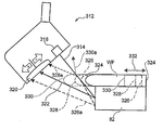
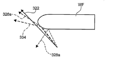
- a detection system for detecting the position of an object mounted on a mounting unit, the light emitting unit capable of outputting detection light for detecting the position of the object, and the light emitting unit from the light emitting unit
- the detection light that is directly incident on the mounting portion is disposed at a position where the reflected light that is generated by being reflected by the mounting portion can be detected, and the detection light that is directly incident on the mounting portion;
- a configuration of a detection system that is located on the opposite side of the reflected light and the object with respect to the detection light directly incident on the mounting unit.
- the detection system detects the position of an object mounted on a mounting unit, the light emitting unit capable of outputting detection light for detecting the position of the object, and the light emitting unit from the light emitting unit
- the detection light that is directly incident on the mounting portion is disposed at a position where the reflected light that is generated by being reflected by the mounting portion can be detected, and the detection light that is directly incident on the mounting portion;
- a configuration of a detection system that is located on the opposite side of the detection light and the object directly incident on the mounting unit with respect to the reflected light.
- the detection system of the twenty-third form or the twenty-fourth form it can be detected that the object having the warped state is correctly mounted at a predetermined position of the transport device or the like.
- a configuration of a transport device that transports the object which has the detection system of the twenty-third or twenty-fourth mode, is employed.
- the detection system of the twenty-third or twenty-fourth embodiment is provided, and the object is a substrate, and a plating apparatus for electrolytically plating the substrate is employed.
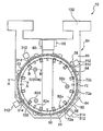
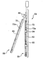
- FIG. 1 is an overall layout view of a plating apparatus including a hand unit and a substrate holder according to an embodiment of the present invention. It is a top view of the substrate holder with which the plating apparatus shown in FIG. 1 is equipped. It is a right view which shows the state which opened the 2nd holding member of the substrate holder shown in FIG. 2 with a virtual line.
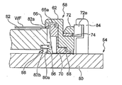
- FIG. 3 is an enlarged sectional view taken along line AA in FIG. 2.
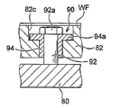
- FIG. 3 is an enlarged sectional view taken along line BB in FIG. 2.
- the processing flow in the curvature amount determination part 170C is shown. A method for measuring the amount of warpage of the substrate in the measurement unit 110 will be described. Another method for measuring the amount of warpage of the substrate will be described.
- FIG. 10C A sectional view of upper stage hand 237 in section AA shown in Drawing 10C is shown. It is a figure which shows the structure of the edge part of a wet hand. It is explanatory drawing of the board
- FIG. It is a graph which shows the elastic member 190 which is a board
- FIG. It is a graph which displays the experimental data for demonstrating the effect of a board
- An air pressure load adjustment mechanism is shown.
- a substrate support member 262 on which a substrate WF is mounted is shown.
- substrate WF is shown.
- 10 shows still another embodiment of a substrate support member on which a substrate WF is mounted. It is a figure explaining operation
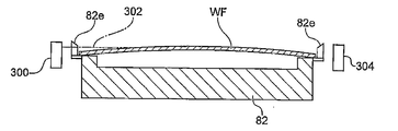
- movement of a horizontal sensor. 7 is a diagram illustrating an example in which a substrate WF having a warped state is erroneously detected even though the substrate WF is correctly mounted at a predetermined position of the substrate holder 18.
- FIG. It is a figure which shows operation
- FIG. 1 shows an overall layout of a plating apparatus that performs plating using a substrate holder according to an embodiment of the present invention.
- the plating apparatus includes a warp amount determination unit 170C that selects a substrate with a small warp amount, a load / unload unit 170A that loads a substrate to the substrate holder 18 or unloads the substrate from the substrate holder 18, and a substrate processing And the processing unit 170B.
- the substrate may be a circular or polygonal semiconductor substrate, and the thickness of the substrate may be, for example, about 1 mm.
- the state where the substrate is warped means that the substrate is not a uniform flat plate without undulations along a horizontal plane.
- the amount of warpage of the substrate is the difference between the maximum value and the minimum value of the distance from the horizontal plane with respect to the upper surface (or lower surface) of the substrate when the substrate is placed on the horizontal plane.
- the load / unload unit 170A has two cassette tables 12 on which a cassette 10 containing a substrate WF such as a semiconductor wafer is mounted, and positions such as an orientation flat and a notch of the substrate WF. And an aligner 14 that matches the direction of the substrate and a spin dryer 16 that dries the substrate WF after the plating process at high speed. Further, near the aligner 14 and the spin dryer 16, there is provided a substrate attaching / detaching portion 20 for placing the substrate holder 18 and attaching / detaching the substrate WF to / from the substrate holder 18. In the center of the cassette table 12, the aligner 14, the spin dryer 16, and the substrate attaching / detaching unit 20, a substrate transfer device (transfer system) 22 including a transfer robot for transferring the substrate WF between them is arranged. .
- a substrate transfer device transfer system
- the processing unit 170B includes, in order from the substrate attaching / detaching unit 20 side, a stocker (wagon) 24 for storing and temporarily placing the substrate holder 18, a prewetting bath 26 for immersing the substrate WF in pure water, and the surface of the substrate WF.
- Two washing tanks 30b and a plating tank 34 are arranged in this order.
- the plating tank 34 is configured by accommodating a plurality of plating units 38 inside an overflow tank 36, and each plating unit 38 accommodates one substrate holder 18 inside and performs plating such as copper plating. It is like that.
- a substrate holder transport unit 40 that employs, for example, a linear motor system is provided that is located on the side of each device and transports the substrate holder 18 together with the substrate WF between these devices.
- the substrate holder transport unit 40 includes a first transporter 42 that transports the substrate WF between the substrate attaching / detaching unit 20 and the stocker 24, a stocker 24, a pre-wet tank 26, a pre-soak tank 28, and washing tanks 30a and 30b.
- a second transporter 44 for transporting the substrate WF between the blow tank 32 and the plating tank 34 is provided.
- a driving device 46 is arranged on the opposite side of the substrate holder transport section 40 across the overflow tank 36.
- the substrate attaching / detaching unit 20 includes two flat plate-like mounting plates 52 that are slidable along the rails 50. A total of two substrate holders 18 are placed in parallel in a horizontal state, one on each of the placement plates 52. The substrate WF is delivered between one of the two substrate holders 18 and the substrate transfer device 22. Thereafter, the mounting plate 52 is slid in the horizontal direction, and the substrate WF is delivered between the other substrate holder 18 and the substrate transport device 22.
- the substrate holder 18 seals the end and back surface of the substrate from the plating solution and exposes the surface to be plated when the substrate is plated. Further, the substrate holder 18 may be provided with a contact for contacting the peripheral portion of the surface to be plated of the substrate and supplying power from an external power source.
- the substrate holder 18 is stored in the stocker 24 (wagon) before the plating process, and is moved between the substrate transfer device 22 and the plating processing unit by the substrate holder transfer unit 40 during the plating process, and is stored again in the wagon after the plating process. Is done.
- the substrate held by the substrate holder 18 is immersed in the plating solution in the plating tank 34 in the vertical direction, and plating is performed while pouring the plating solution from below the plating tank 34 to cause overflow.
- the plating tank 34 preferably includes a plurality of plating units 38.
- each plating unit 38 one substrate holder 18 holding one substrate is immersed vertically in a plating solution, and plating is performed. Is done.
- Each plating unit 38 preferably includes an insertion portion for the substrate holder 18, a current-carrying portion for the substrate holder 18, an anode, a paddle stirring device, and a shielding plate.
- the anode is used by being attached to an anode holder, and the exposed surface of the anode facing the substrate is concentric with the substrate.
- the substrate held by the substrate holder 18 is processed with a processing fluid in each processing tank of the plating processing unit.
- the substrate held by the substrate holder 18 is processed with a processing fluid in each processing tank of the plating processing unit.
- the arrangement of each treatment tank in the plating treatment unit is, in order of process, a pre-water washing tank, a pretreatment tank, a rinse tank, a first plating tank, and a rinse.
- An arrangement such as a tank, a second plating tank, a rinse tank, or a blow tank may be employed, or another configuration may be employed. It is preferable to dispose each processing tank in the order of steps (X ⁇ X ′ direction) in order to eliminate an extra conveyance path.
- the kind of tank, the number of tanks, and the arrangement of the tanks in the plating apparatus can be freely selected according to the purpose of processing the substrate.
- the first transporter 42 and the second transporter 44 of the substrate holder transport unit 40 have an arm for suspending the substrate holder, and the arm has a lifter for holding the substrate holder 18 in a vertical posture.
- the substrate holder transport unit is movable along the travel axis between the substrate attaching / detaching unit 20 and the plating processing unit by a transport mechanism (not shown) such as a linear motor.
- the substrate holder transport unit 40 holds and transports the substrate holder 18 in a vertical posture.
- a stocker for storing substrate holders can store a plurality of substrate holders 18 in a vertical state.
- the substrate holder 18 can be opened and closed by a rectangular flat plate-shaped first holding member (fixed holding member) 54 made of, for example, vinyl chloride, and the first holding member 54 via a hinge 56. And a second holding member (movable holding member) 58 attached thereto.
- first holding member fixed holding member
- second holding member movable holding member
- the second holding member 58 has a base 60 and a ring-shaped seal holder 62, and is made of, for example, vinyl chloride to improve sliding with the presser ring 72 described below.
- the surface of the seal holder 62 facing the first holding member 54 is pressed against the outer peripheral portion of the substrate WF along the substrate seal line 64 of the outer peripheral portion of the substrate WF.
- a substrate sealing member 66 is attached to protrude inward.
- a holder seal member 68 that seals the surface of the seal holder 62 that faces the first holding member 54 by pressing against the following support base 80 of the first holding member 54 at a position outward of the substrate seal member 66. Is installed.
- the substrate seal member 66 and the holder seal member 68 are attached to the seal holder 62 by being sandwiched between the seal holder 62 and a fixing ring 70 attached to the seal holder 62 via a fastener such as a bolt.
- a fastener such as a bolt.
- a step portion is provided on the outer peripheral portion of the seal holder 62 of the second holding member 58, and a presser ring 72 is rotatably attached to the step portion via a spacer 74.
- the presser ring 72 is mounted so that it cannot be removed from the seal holder 62 by a presser plate (not shown) attached to the side surface of the seal holder 62 so as to protrude outward.
- the presser ring 72 is made of, for example, titanium having excellent corrosion resistance against acid and sufficient rigidity.
- the spacer 74 is made of a material having a low coefficient of friction such as PTEF so that the presser ring 72 can rotate smoothly.
- the first holding member 54 has a substantially flat plate shape and has a support base 80 that presses against the holder seal member 68 and seals between the second holding member 58 when the substrate WF is held by the substrate holder 18. Further, the first holding member 54 has a substantially disc-shaped movable base (support portion) 82 separated from the support base 80. Located on the outer side of the presser ring 72, the support base 80 of the first holding member 54 is provided with inverted L-shaped clampers 84 having protruding portions protruding inward at equal intervals along the circumferential direction. It is installed. On the other hand, a protrusion 72 a that protrudes outward is provided at a position facing the clamper 84 along the circumferential direction of the presser ring 72.
- the lower surface of the inwardly protruding portion of the clamper 84 and the upper surface of the protrusion 72a of the holding ring 72 are tapered surfaces that are inclined in opposite directions along the rotation direction.
- potches 72b that protrude upward are provided. Accordingly, the presser ring 72 can be rotated by rotating a rotary pin (not shown) and pushing the potch 72b from the side and turning it.
- the sandwiching of the substrate WF is performed according to the following procedure. As indicated by phantom lines in FIG. 3, with the second holding member 58 opened, the substrate WF is inserted into the center of the first holding member 54, and the second holding member 58 is closed via the hinge 56. Then, the presser ring 72 is rotated clockwise, and the protrusion 72 a of the presser ring 72 is slid into the inner protrusion of the clamper 84. As a result, the first holding member 54 and the second holding member 58 are fastened and locked to each other through the tapered surfaces provided on the protrusion 72a of the presser ring 72 and the clamper 84, respectively.
- the presser ring 72 When releasing the lock, the presser ring 72 is rotated counterclockwise, and the protrusion 72 a of the presser ring 72 is pulled out from the inwardly protruding portion of the inverted L-shaped clamper 84. In this way, the lock can be released.
- the movable base 82 has a ring-shaped edge portion 82a that supports the substrate WF by contacting the outer periphery of the substrate WF when the substrate WF is held by the substrate holder 18.
- the edge portion 82 a is attached to the support base 80 via a compression spring 86 so as to be movable in a direction close to the support base 80.
- the edge portion 82 a is biased in a direction away from the support base 80 by the biasing force (spring force) of the compression spring 86.
- a thickness absorbing mechanism 88 that absorbs the thickness of the substrate WF by moving the movable base 82 in the direction of approaching the support base 80 according to the thickness of the substrate WF when the substrates WF having different thicknesses are held by the substrate holder 18. Is configured.
- a substrate guide 82e for guiding the outer peripheral end of the substrate W to position the substrate W with respect to the movable base 82.
- the outer peripheral end of the substrate WF is guided by the substrate guide 82 e, and the substrate WF is positioned relative to the movable base 82. Is done.
- the type of the plating solution is not particularly limited, and various plating solutions are used depending on the application.
- the plating solution in the case of a plating process for TSV can be used.
- a plating solution containing CoWB (cobalt, tungsten, boron), CoWP (cobalt, tungsten, phosphorus), or the like for forming a metal film on the surface of the substrate having Cu wiring may be used.
- a plating solution for forming a barrier film provided on the surface of the substrate or the concave portion of the substrate before the Cu wiring is formed for example, CoWB or Ta
- a plating solution containing (tantalum) may be used.
- the plating processing system including a plurality of plating processing apparatuses configured as described above has a controller (not shown) configured to control the above-described units.
- the controller includes a memory (not shown) that stores a predetermined program, a CPU (Central Processing Unit) (not shown) that executes the program in the memory, and a control unit that is realized by the CPU executing the program ( (Not shown).
- the control unit can perform, for example, transport control of the substrate transport device 22, transport control of the substrate holder transport unit 40, and control of the plating current and plating time in the plating tank 34.
- the controller is configured to be communicable with a host controller (not shown) that performs overall control of the plating apparatus and other related apparatuses, and can exchange data with a database included in the host controller.
- the storage medium constituting the memory stores various setting data and various programs such as a plating processing program to be described later.
- a known medium such as a computer-readable memory such as ROM or RAM, or a disk-shaped storage medium such as a hard disk, CD-ROM, DVD-ROM, or flexible disk can be used.
- a substrate having a small warpage is selected by the warpage amount determination unit 170C provided in the plating apparatus.
- the selected substrate is stored in the cassette table 12.
- the warpage amount determination unit 170C includes a measurement unit 110 that measures the warpage amount of the substrate and a FOUP (Front-Opening / Unified / Pod).
- FOUP is a carrier for 300mm wafer transportation and storage, and is a front-opening cassette-integrated transportation and storage box.
- FIG. 6 shows a processing flow in the warp amount determination unit 170C.
- the measurement unit 110 measures the amount of warpage of the substrate taken out from the FOUP 112 (step 114). Note that the transfer of the substrate between the FOUP 112 and the measurement unit 110 and the transfer of the substrate between the measurement unit 110 and the cassette table 12 are performed by a transfer robot (not shown). It is determined whether the measured amount of warpage of the substrate is less than a threshold value (step 116). For example, the threshold value is 2 mm. When the warpage amount of the substrate is less than the threshold value, the substrate is sent to the cassette table 12 in order to mount the substrate on the substrate holder 18 and perform plating (step 118). When the warpage amount of the substrate is equal to or greater than the threshold value, an error is issued to the control unit and the substrate is returned to the FOUP 112 (step 120). As a result, the substrate WF having a large warp can be stopped before being cracked.
- a threshold value is 2 mm.
- the substrate WF is mounted on the rotation stage 122, and the substrate WF is rotated.
- the distance sensor 124 measures the amount of warpage of the substrate WF.
- the distance sensor 124 is disposed on the outer periphery of the substrate WF.
- the distance sensor 124 reads the distance between the distance sensor 124 and the substrate WF.
- the distance sensor 124 further outputs the amount of change in the distance on the outer periphery of the substrate WF to the controller with reference to the distance between the distance sensor 124 and the substrate WF at the measurement start point of the substrate WF.
- the controller does not perform the plating process when the amount of change in the distance on the outer periphery of the substrate WF is equal to or greater than a certain threshold value, and does not mount the substrate WF on the substrate holder.
- the distance sensor 124 since the distance sensor 124 is fixed, only the amount of change in the distance on the outer periphery of the substrate WF is measured.
- the distance sensor 124 moves on the substrate WF in the radial direction of the substrate WF while rotating the substrate WF. Accordingly, the distance sensor 124 measures the amount of change in the distance between the circumferential direction and the radial direction of the substrate WF.
- a plurality of distance sensors 124 may be arranged in the radial direction. When only the amount of change in the distance on the outer periphery is measured, the entire substrate WF has a warp, but the warp may not be detected on the outer periphery.
- the substrate is warped in a chevron or bowl shape.
- the warp is detected by measuring the distance between the distance sensor 124 and the upper surface of the rotary stage 122 in advance.
- the warp is not detected only by measuring the amount of change in the distance on the outer periphery.
- the distance sensor 124 preferably measures the amount of change in the distance between the circumferential direction and the radial direction of the substrate WF.
- a laser distance meter can be used as the distance sensor 124.
- the laser distance meter measures the distance by measuring the time until the irradiated light is reflected and received by the measurement object.
- phase difference distance method and “pulse propagation method” depending on the measurement method.
- FIG. 8 shows another method for measuring the warpage amount of the substrate WF.
- a profile measuring instrument 126 that can measure over the radius of the substrate WF is used.
- the profile measuring instrument 126 is fixed.
- the profile of the amount of change in the distance on the outer periphery of the substrate WF is measured by rotating the substrate WF on the stage such as the aligner 14 shown in FIG. Yes.
- FIG. 8B shows an example of a profile that is a measurement result of the amount of change in distance over the entire substrate WF.
- FIG. 8B shows the measurement result of the amount of change in the distance on one diameter.
- the horizontal axis indicates the position on the diameter of the substrate WF, and the vertical axis indicates the amount of change in distance.
- the controller determines the amount of warpage of the substrate from the amount of change in the distance on the outer periphery of the substrate or over the entire substrate.
- the substrate WF having a certain warping amount for example, the substrate WF having a warping amount of 2 mm is not processed.
- a determination unit 170C may be provided, and the profile measuring instrument 126 may be used in the determination unit 170C.
- FIG. 9 shows another method for measuring the warpage amount of the substrate WF.
- the distance sensor 124 scans the outer periphery of the substrate WF to measure the distance between the substrate WF and the distance sensor 124.
- the distance sensor 124 is rotated on the outer periphery of the substrate WF on the placement plate 52, and the profile of the change in distance over the entire substrate WF is measured.
- a plurality of sensors 124 may be arranged on the outer periphery of the substrate WF, and the distance sensor 124 may be fixed.
- the distance between the distance sensor 124 and the upper surface 128 of the edge portion 82a of the movable base 82 is measured in advance, if there is a warp on the outer periphery, the warp on the outer periphery is detected.
- FIG. 9A is an example in which the substrate WF is warped in a bowl shape (valley shape), and FIG. 9B is an example in which the substrate WF is warped in a mountain shape.
- FIG. 9A and FIG. 9B are examples in which the warpage amount is less than the threshold value.
- FIG. 9A and FIG. 9B are examples in which the movable base 82 has an edge portion 82a that contacts the back surface of the substrate WF located on the outer peripheral portion of the substrate WF, and a recess 130 other than the edge portion 82a. is there.
- the recess 130 is recessed with respect to the edge portion 82a in a direction away from the back surface of the substrate WF.
- the depth of the recess is, for example, 2.5 mm.
- FIG. 9C is a comparative example in which the movable base 82 does not have the concave portion 130 described above.
- the concave portion 130 if the warpage amount is within the threshold value, plating can be performed in either a mountain shape or a valley shape, as shown in FIGS. 9 (a) and 9 (b).
- the force for holding the substrate WF is applied to the edge portion 82a as described above. Strain is generated and the possibility of breakage is greater than in the case of FIG. In the case of FIGS. 9A and 9B, even if the force for holding the substrate WF is applied to the edge portion 82a as described above, the possibility that the substrate WF is distorted is low.
- FIG. 10A is a plan view showing the substrate transfer device 22 (however, the upper hand 237 (hand unit) holds the substrate WF), and FIG. 10B is a side view of the substrate transfer device 22 (the substrate WF is shown).
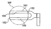
- FIG. 10C is a plan view of the main part of the upper hand 237 of the substrate transport apparatus 22 (state in which the substrate WF is held), and FIG. 10D is a main part of the lower hand (hand part) 241 of the substrate transport apparatus 22 It is a top view (state which hold
- the substrate transfer device 22 is arranged at the top of one arm 233 of a plurality (two sets) of arms 233 and 235 having a plurality of joints installed on the substrate transfer device main body 231.
- a hand 237 is attached.
- the substrate transfer device 22 has a lower hand 241 attached to the tip of the other arm 235.
- the upper hand 237 is a dry hand that transports a dry substrate WF from the cassette table 12 to the placement plate 52.
- the upper hand 237 is mounted so that the surface of the substrate WF is on the upper side, the thickness of the upper hand 237 is 10 mm or less, and the back surface of the substrate WF is vacuum-sucked.
- the lower hand 241 is a wet hand that transports the substrate W transported from the plating processing unit 170 ⁇ / b> B to the placement plate 52 to the spin dryer 16.
- the lower hand 241 is mounted such that the surface of the substrate WF is on the lower side.
- the substrate WF is mounted on the support part 220 surrounded by the peripheral wall part 152.
- the upper hand 237 includes a base 132 and two protrusions 134 disposed on the surface of the base 132.
- Base 132 is formed from two forks.
- the base 132 may be composed of three or more forks.
- the protrusion 134 has a vacuum hole 136 communicating with a vacuum source (not shown).
- the vacuum hole 136 has an opening 138 at the top of the protrusion 134, and the top of the protrusion 134 is the surface 140 of the base 132.
- the height is fixed.
- the substrate WF is adsorbed on the top of the protrusion 134 by vacuum.
- the top of the protrusion 134 has a height 142 (shown in FIG. 11) of 1 mm to 2 mm with respect to the surface of the base 132.
- the protrusion 134 is disposed at the center of the surface 140.
- the protrusion 134 is 2 mm higher than the surface of the base 132 in consideration that the amount of warping of the substrate WF to be sucked is 2 mm or less.
- FIG. 11 shows a cross-sectional view of the upper hand 237 in the cross-section AA shown in FIG. 10C.
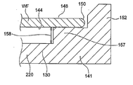
- the lower hand (hand portion) 241 is a portion (recessed portion 130) facing the lower surface (back surface 144) of the substrate WF in consideration of the warpage amount of the substrate WF to be mounted being 2 mm or less. ) Is dug down to the edge portion 157 by 2 mm.
- the substrate WF has a front surface 148, a back surface 144, and a side surface 150 located on the outer periphery of the substrate WF.
- the lower hand 241 includes a support portion 220 that faces the back surface 144 of the substrate WF and mounts the substrate WF, and a peripheral wall portion 152 that faces the side surface 150 of the substrate WF and is disposed on the outer periphery of the support portion 220. Have.
- the support part 220 has an edge part 157 that contacts the back surface 144 located on the outer peripheral part 160 of the substrate WF, and a concave part 130 other than the edge part 157.
- the recess 130 is recessed with respect to the edge portion 157 in a direction away from the back surface 144.
- the lower hand 241 is formed from two forks 156.
- the lower hand 241 may be composed of three or more forks.
- the peripheral wall portion 152 is provided on the fork portion 156.
- the recess of the recess 130 has a depth 158 of 1 mm to 2 mm.
- the depth 158 is preferably 0.5 mm or more.
- the substrate holder 18 includes a first holding member 54 and a second holding member 58 that detachably hold the substrate WF with the outer peripheral portion 160 of the substrate WF interposed therebetween.
- the first holding member 54 has a movable base 82 that faces the back surface 144 of the substrate WF.
- the substrate holder 18 includes a substrate holding member (back side support) 162 that applies a force to the back surface 144 of the substrate WF facing the first holding member 54 in a direction from the movable base 82 toward the substrate WF.
- one substrate holding member (backside support) 162 can be provided at a position corresponding to the central portion of the substrate, at least three substrate holding members (backside supports) may be provided evenly in the circumferential direction near the central portion of the substrate.
- the substrate holding member (backside support) 162 is connected to the first holding member 54 by an elastic member 184 such as a leaf spring, and is fixed to be stretchable in a direction perpendicular to the substrate surface. it can.
- At least three elastic members 184 can be equally arranged in the circumferential direction.
- the movable base 82 is connected to the first holding member 54 by an elastic member 86 such as a leaf spring, and can be fixed to be stretchable in the direction perpendicular to the substrate surface.
- At least three elastic members 86 can be equally arranged in the circumferential direction.
- the lengths of the elastic member 86 and the elastic member 184 are such that the movable base 82 is lowered and the central substrate holding member 162 protrudes to the same height as the outer periphery. Is adjusted.
- the degree of warping of the substrate WF is small, it is not necessary to secure the protruding amount of the substrate holding member 162 so that a simple connecting member is provided instead of providing the elastic member 86, and the elastic member 184 is provided. Only can be provided.
- the movable base 82 and / or the substrate holding member 162 is connected to the first holding member 54 by an elastic body, the influence of the unevenness of the object to be held such as warping of the substrate can be absorbed, and the thickness is increased. Even such a substrate WF can be held while absorbing the influence of the thickness of the substrate.
- the substrate holder in the present embodiment may be configured not to include the thickness absorbing mechanism 88 that absorbs the thickness of the substrate WF described above.
- the substrate holder 18 Since the space 164 existing on the back surface 144 side of the substrate WF is the sealed space 164, the pressure in the space 164 is lower than the water pressure.
- the substrate holder 18 has a substrate holding member 162 for resisting water pressure applied to the surface 148 of the substrate WF during the plating process. For this reason, the crack of the substrate WF can be prevented.
- the movable base 82 has a through hole 172.
- the opening 174 of the through hole 172 faces the back surface 144 of the substrate WF.
- the substrate holding member 162 is disposed in the through hole 172.
- the movable base 82 has an edge part 82a that contacts the back surface 144 located on the outer peripheral part 160 of the substrate WF, and a concave part 130 other than the edge part 82a.
- the recessed part 130 is recessed with respect to the edge part 82a in the direction away from the back surface 144.
- FIG. 13A shows a state before the substrate WF is placed on the first holding member 54 and the second holding member 58 sandwiches the substrate WF.
- FIG. 13B shows a state after the substrate WF is sandwiched between the second holding members 58.
- the portion 180 where the substrate holding member main body 186 contacts the back surface 144 is not exposed from the surface of the recess 130.
- the substrate holding member main body 186 is locked by the locking portion 188.
- the substrate holding member main body 186 is movable in the through hole 172 in the direction from the recess 130 toward the WF substrate and in the direction from the substrate WF toward the recess 130.
- the substrate holding member body 186 pushes the back surface 144 to correct the warpage of the substrate WF. For this reason, the portion 180 where the substrate holding member main body 186 contacts the back surface 144 and the portion where the edge portion 82a contacts the back surface 144 are measured in the direction from the point on the recess 130 toward the substrate WF from the recess 130. 182 is the same. That is, when the substrate WF is gripped, the movable base 82 is lowered, the central substrate holding member 162 protrudes, and becomes the same height as the outer periphery.
- the height is not the same height as the outer periphery but can support the substrate in consideration of the known warpage amount.
- a substrate holding member 162 that is a backside support that supports the substrate WF from the back surface is provided.
- the movable base 82 and / or the substrate holding member 162 are connected to the first holding member 54 by an elastic body. Therefore, when immersed in the plating solution while holding the warped substrate WF, the amount of warpage can be prevented from increasing due to water pressure, and cracking of the substrate can be prevented. Furthermore, even if the substrate WF is not warped so much when held by the substrate holder, the substrate WF held by the substrate holder is warped in the plating solution due to the influence of water pressure after being immersed in the plating solution. Therefore, it is possible to effectively prevent the substrate from being cracked during the plating process.
- FIG. 14 shows an elastic member 190 that is a substrate holding member that is preferably applied when it is not preferable to correct the state without warping.
- the elastic member 190 is disposed between the concave portion 130 of the movable base 82 and the back surface 144 of the substrate WF.
- the elastic member 190 is an airbag, for example, and supports the substrate WF from the back surface 144.
- the elastic member 190 can support the substrate WF with a constant pressure.
- FIG. 14 shows the case of a substrate warped in a chevron, but in the case of a substrate warped in a bowl shape, an airbag is disposed on the outer periphery of the substrate.
- the substrate is supported by deforming the substrate into a bowl shape by applying pressure to the outer periphery of the substrate so as to push (protrude) upward in FIG.
- the height of the donut-shaped airbag is adjusted using the profile data measured in advance by the method described in FIGS. 7 and 8 to support the substrate. In this way, the load applied to the substrate can be reduced and the substrate can be supported from the back side.
- FIG. 15 shows another substrate holding member that is preferably applied when it is not preferable to correct the state without warping.
- the substrate holding member is a backside support for resisting water pressure.
- the substrate holding member has five variable length members 192.
- the variable length member 192 is disposed between the concave portion 130 of the movable base 82 and the back surface 144 of the substrate WF, and the length 294 in the direction from the concave portion 130 of the movable base 82 toward the substrate WF can be adjusted.
- the variable length member 192 has a pin shape, for example.
- the length 294 of the variable length member 192 is adjusted according to the distance between the concave portion 130 of the movable base 82 and the back surface 144 of the substrate WF where the variable length member 192 is installed. Normally, the length 294 of the variable length member 192 is made to coincide with this distance.
- the adjustment method uses the profile data measured in advance by the method described with reference to FIGS. 7 and 8, and projects the variable length member 192 from the bottom so as to match the profile. Specifically, the measured profile data is stored in a memory of a controller (not shown) of the plating apparatus described above, and the CPU executes a program so that a plurality of variable length members 192 provided on the substrate holder 18 are provided. Control to adjust the length of each.
- an air pressure or spring force is applied to the variable length member 192 from below the variable length member 192, and an air pressure load adjustment mechanism or a spring force load adjustment mechanism that adjusts the air pressure or spring force.
- an air pressure load adjustment mechanism or a spring force load adjustment mechanism that adjusts the air pressure or spring force.
- an electromagnetic actuator using an electromagnetic force generated by a coil and a piezoelectric actuator using a piezoelectric effect can also be used as the adjustment mechanism.
- FIG. 21 shows the air pressure load adjusting mechanism 240.
- FIG. 21A shows the air pressure load adjusting mechanism 240 when the substrate WF is mounted on the substrate holder 18.
- FIG. 21B shows the air pressure load adjusting mechanism 240 before the substrate WF is mounted on the substrate holder 18.
- the air pressure load adjusting mechanism 240 houses a part of the variable length member 192 in the cylinder 244, and the upper portion of the variable length member 192 is outside the cylinder 244.
- the variable length member 192 has a pin shape.
- the top 246 of the variable length member 192 contacts the back surface (lower surface) of the substrate WF.
- a spring 242 is disposed between the flange 248 of the variable length member 192 and the upper surface 250 of the cylinder 244.
- the spring 242 generates a force that pushes down the variable length member 192 downward.
- Air is supplied into the cylinder 244 from an intake port 252 provided in the lower portion of the cylinder 244. By controlling the pressure of the air in the cylinder 244, the protruding amount of the variable length member 192 is controlled.
- a pressure sensor 254 is provided at the top 246 of the variable length member 192.
- the pressure sensor 254 detects the pressure acting between the variable length member 192 and the substrate WF.
- the air pressure in the cylinder 244 is adjusted by using the pressure detected by the pressure sensor 254 and acting between the variable length member 192 and the substrate WF. As a result, the pressure acting between the variable length member 192 and the substrate WF can be adjusted.
- the pressure sensor 254 can feedback control the pressure acting between the variable length member 192 and the substrate WF.
- the pressure sensor 254 is a semiconductor pressure sensor using a piezoresistance effect, for example.
- Air having a predetermined air pressure may be supplied without using the pressure sensor 254.
- FIG. 22 shows another embodiment of the air pressure load adjusting mechanism 240.
- FIG. 22A shows the air pressure load adjusting mechanism 240 when the substrate WF is mounted on the substrate holder 18.
- FIG. 22B shows the air pressure load adjusting mechanism 240 before the substrate WF is mounted on the substrate holder 18.
- the air pressure load adjusting mechanism 240 is a fixed length method (fixed spring force method). Prior to mounting the substrate, the variable length member 192 is pushed down by air pressure. While the substrate WF is clamped, the air is removed and the variable length member 192 is pushed up by the spring 242.
- a spring 242 is disposed between the flange 248 of the variable length member 192 and the lower surface 256 of the cylinder 244.
- the spring 242 generates a force that pushes up the variable length member 192 upward.
- Air is supplied into the cylinder 244 from an intake port 252 provided in the upper part of the cylinder 244.
- variable length member 192 As shown in FIG. 22B, before the substrate WF is mounted, air is supplied from the air inlet 252 and the variable length member 192 is lowered downward by the force of air pressure. As shown in FIG. 22A, after mounting the substrate WF, air is extracted from the air inlet 252 and the variable length member 192 is raised upward by the force of the spring 242. The protruding amount of the variable length member 192 is determined only by the spring force.
- a pressure sensor may be installed at the tip of the variable length member 192 to measure the contact pressure between the variable length member 192 and the back surface 144 of the substrate WF. Then, the variable length member 192 is protruded toward the back surface 144 until the contact pressure reaches a predetermined magnitude, and the variable length member 192 is fixed at that position. In this case, the position of the variable length member 192 can be set without using the profile data.
- the control unit displays and / or outputs an error signal.
- the control unit may accumulate an error signal.
- the control unit may control the position of the variable length member 192 during plating so that the contact pressure is constant.
- FIG. 15 can have a pin shape or an island shape.
- An example of an island-shaped variable length member 192 is shown in FIG. FIG. 16 is a plan view of the movable base 82.
- the variable length members 192 are arranged concentrically on the movable base 82.
- the variable length member 192a disposed on the inner circumference includes two variable length members 192a.
- the variable length member 192b disposed on the outer circumference is composed of six variable length members 192b. In order to guide the movement of the variable length member 192b, six guides 202 are equally arranged around the variable length member 192b.
- the movable base 82 has a recess 130.
- the movable base 82 has no recess.
- the substrate WF does not have a gap on the surface of the movable base 82 Adhere to. This is because the liquid enters between the surface of the movable base 82 and the substrate WF.
- FIGS. 13 to 16 when the substrate holding member is provided, there is an advantage that the substrate WF can be prevented from adhering to the surface of the movable base 82 without a gap.
- FIGS. 17 and 18 show graphs displaying experimental data for explaining the effect of the substrate holding member.
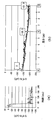
- FIGS. 17A and 17B show strain data generated on the substrate WF during plating when there is no substrate holding member.
- the horizontal axis represents the elapsed time from the start of plating
- the vertical axis represents the strain amount in ⁇ ST.
- the horizontal axis represents the plating thickness from the start of plating, the thickness at the start of plating is 0 ⁇ m
- the vertical axis represents the strain amount in ⁇ ST.
- FIG. 18 shows strain data generated on the substrate WF during plating when there is a substrate holding member.
- the horizontal axis represents the elapsed time from the start of plating
- the vertical axis represents the strain amount in ⁇ ST.
- FIG. 17A shows strain when the substrate holding member 162 shown in FIG. 13 is used.
- a graph 194 is a strain when the substrate holding member 162 is used, and a graph 196 is a strain when the substrate holding member 162 is not used.
- the graph 194 includes three graphs with different numbers of paddle reciprocations.
- the graph 196 is composed of six graphs with different numbers of paddle reciprocations.
- the upper solid line graph corresponds to the lower solid line graph, and these are graphs when the number of reciprocations of the paddle is 375 rpm.
- the upper dotted line graph corresponds to the lower dotted line graph, and these are graphs when the number of paddle reciprocations is 300 rpm, and the upper dashed line graph corresponds to the lower dashed line graph. These are graphs when the number of reciprocations of the paddle is 225 rpm.
- the upper graph is the maximum value of the distortion when the number of reciprocations of paddles is the upper graph
- the minimum value of the distortion when the lower graph is the number of reciprocations of paddles.
- the lock mechanism pushes down the presser ring 72 that is a component of the second holding member 58 (specifically, the presser ring 72 that is a component of the seal holder 62).
- the lock mechanism rotates the presser ring 72 clockwise, and slides the protrusion 72 a of the presser ring 72 into the inner projecting portion of the clamper 84. In this way, the first holding member 54 and the second holding member 58 are tightened and locked together. After locking, the lock mechanism moves away from the presser ring 72.
- the lock mechanism When releasing the lock, perform a similar operation except that the rotation direction is different. That is, the lock mechanism pushes the presser ring 72 downward. Next, the lock mechanism rotates the presser ring 72 counterclockwise so that the protrusion 72 a of the presser ring 72 is taken out from the inside of the inward protruding part of the clamper 84. As a result, the first holding member 54 and the second holding member 58 are opened. Thereafter, the lock mechanism moves away from the presser ring 72.
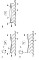
- FIGS. 19A and 19B show the case where the lock is performed, and FIG. 19A shows the case where the speed at which the lock mechanism is separated from the presser ring 72 is high. FIG. 19B shows a case where the speed at which the lock mechanism moves away from the presser ring 72 is low.
- FIG. 19A illustrates a procedure when the speed at which the lock mechanism is separated from the seal holder 62 is high.
- the lock mechanism 204 engages with the seal holder 62 (S10), and moves down together with the seal holder 62 at a speed of 2500 mm / min (S12).
- the speed is decreased and the substrate is lowered at a speed of 50 mm / min (S14).
- the seal holder 62 comes into contact with the substrate WF, the seal holder 62 is further pressed downward (S16), and then the presser ring 72 is rotated clockwise, so that the protrusion 72a of the presser ring 72 is moved inwardly of the clamper 84. (S18).
- the lock mechanism 204 moves away from the presser ring 72 at a high speed of 3000 mm / min (S20).
- FIG. 19B illustrates a procedure when the speed at which the lock mechanism 204 moves away from the presser ring 72 is low. Steps S10 to S18 are the same as those in FIG. After step S18, the lock mechanism leaves the presser ring 72 at a low speed of 50 mm / min (S22). After the lock mechanism 204 is completely separated from the ring 72, the lock mechanism 204 is separated from the presser ring 72 at a high speed of 3000 mm / min (S24), as in step S20 of FIG.
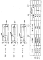
- FIGS. 19A and 19B show the strain when the speed at which the locking mechanism is separated from the seal holder 62 is high, and FIG. 20 (b) shows the strain when the speed at which the locking mechanism is separated from the seal holder 62 is low. Show. 20 (a) and 20 (c) correspond to FIG. 19 (a), and FIG. 20 (b) corresponds to FIG. 19 (b). 20 (a) to 20 (c), the horizontal axis represents time, and the vertical axis represents strain. 20A and 20C, the speed at which the lock mechanism moves away from the seal holder 62 is the same, but the torque of the motor of the lock mechanism is different.
- a point 206 indicates a strain when the seal holder 62 contacts the substrate WF. The strain increases rapidly from “0 ⁇ ST” to “100 ⁇ ST”. A point 208 indicates a strain when the seal holder 62 is separated from the substrate WF. The strain decreases from “50 ⁇ ST” to “ ⁇ 25 ⁇ ST”. The fact that the strain has changed from positive to negative means that the direction of warping of the substrate WF has been reversed. That is, it means that a large strain has occurred in the substrate WF. A “star” indicated by a point 206 indicates that a large impact force is applied to the substrate WF at this time.
- the point 210 indicates the strain when the seal holder 62 is separated from the substrate WF, but the strain decreases from “50 ⁇ ST” to “0 ⁇ ST”.
- the fact that the strain has changed from positive to zero means that the warping direction of the substrate WF is not reversed. That is, it means that a large strain is not generated in the substrate WF.
- FIGS. 20 (d) to 20 (f) correspond to FIGS. 20 (a) to 20 (c), and the seal holder 62 in FIGS. 20 (a) to 20 (c) is separated from the substrate WF.
- the maximum value 216 and the minimum value 218 of the strain at the speed 212, the motor torque 214, and the points 208 and 210 are shown.
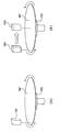
- FIG. 23A shows a plan view of the substrate support member 262 on which the substrate WF is mounted.
- FIG.23 (b) shows AA sectional drawing of Fig.23 (a).
- the substrate support member 262 can stably adsorb the substrate WF warped in a bowl shape.
- the substrate support member 262 that supports the substrate WF of the present embodiment is provided on the base 258, the surface 272 of the base 258, the three support portions 260 on which the substrate WF is mounted, and the surface 272 of the base 258. And a protruding portion (vacuum chuck portion) 264 disposed on the top.
- the outer diameter of the substrate support member 262 has a smaller diameter than the diameter of the substrate WF for detecting notches on the outer periphery of the substrate WF and detecting the outer periphery.
- the protrusion 264 has a vacuum hole 266 for adsorbing the substrate WF by vacuum.
- the vacuum hole 266 has an opening 270 at the top 268 of the protrusion 264.
- a height 274 of the top 268 of the protrusion 264 is fixed to the surface 272 of the base 258.
- the substrate WF is adsorbed to the top 268 of the protrusion 264 by vacuum.
- the vacuum hole 266 is connected to a vacuum source 276 that is a vacuum pump.
- the protrusion 268 is disposed at the center of the base 258.
- Three support portions 260 are provided in the present embodiment, but may be three or more.
- the substrate support member 262 includes substrate support portions 260 at three locations so as to contact the outer periphery of the substrate WF.
- the substrate support member 262 can stably adsorb the substrate WF warped in a bowl shape.
- FIG. 24A shows a plan view of the substrate support member 278.
- FIG. 24B shows an AA cross-sectional view of FIG. 24A when the substrate WF is mounted.
- the substrate support member 278 is capable of stably adsorbing the substrate WF that is warped in a mountain shape.
- the substrate support member 278 that supports the substrate WF of this embodiment has a base 280 and a vacuum hole 266 for the base 280 to adsorb the substrate WF by vacuum.
- the vacuum hole 266 has an opening 284 at the top 282 of the base 280.
- the substrate WF is adsorbed to the top 282 of the base 280 by vacuum.
- a base portion 280 that is a protrusion protruding from the support portion 286 is provided at a portion that contacts the center of the substrate WF.
- At the top 282 of the base 280 is an opening 284 for vacuum suction.
- the vacuum hole 266 is connected to the vacuum source 276. This substrate support member can stably adsorb the substrate warped in a mountain shape.
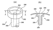
- FIG. 25A shows a plan view of the substrate support member 288.
- FIG. 25B shows a cross-sectional view taken along line AA in FIG. 25A when the substrate WF is mounted.
- the substrate support member 288 is capable of stably adsorbing the substrate WF that is warped in a mountain shape.
- the substrate support member 288 that supports the substrate WF of this embodiment has a base 290 and a vacuum hole 292 for the base 290 to adsorb the substrate WF by vacuum.
- the vacuum hole 292 has an opening 298 at the top 296 of the base 290.
- the substrate WF is adsorbed to the top 296 of the base 290 by vacuum.
- a base portion 290 that is a protruding portion protruding from the support portion 286 is provided at a portion that contacts the center of the substrate WF.
- This substrate support member can stably adsorb the substrate warped in a mountain shape.
- the vacuum hole 292 is connected to the vacuum hole 266.
- the vacuum hole 266 is connected to the vacuum source 276.
- a detection system capable of detecting that a substrate WF having a warped state is correctly mounted at a predetermined position such as a transfer device (substrate holder 18) will be described.
- a horizontal sensor can be used to detect whether the substrate WF is correctly placed on the substrate support member for transport.
- the operation of the horizontal sensor that can be applied to the substrate WF that does not have a warped state will be described with reference to FIG.
- the operation of the horizontal sensor that can be applied to the substrate WF having a warped state will be described later.
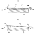
- FIG. 26A is an explanatory diagram of the operation of the horizontal sensor when the substrate WF that does not have a warped state is installed at the correct position on the movable base 82.
- FIG. 26B is an explanatory diagram illustrating the operation of the horizontal sensor when the substrate WF that does not have a warped state is installed at an inappropriate position on the movable base 82.
- the light emitting unit 300 of the horizontal sensor emits the light beam 302 so that the light beam 302 passes slightly above the substrate WF.
- the light beam 302 is detected by the detection unit 304 of the horizontal sensor.
- FIG. 26B when a substrate WF that does not have a warp is installed at an inappropriate position on the movable base 82, specifically, on the substrate guide 82e, the light beam 302 is emitted from the substrate 302. Blocked by WF. Since the detection unit 304 does not detect the light beam 302, it can detect that the substrate WF is installed at an inappropriate position on the movable base 82. Note that the light emitting unit 300 and the detection unit 304 are arranged at positions where the light beam 302 is not blocked by the substrate guide 82e.
- the light emitting unit 300 and the detecting unit 304 are preferably arranged on two diameters of the substrate WF.
- the angle formed by the two diameters is preferably 90 degrees, but may be larger than 0 degrees.
- the light emitting unit 300 and the detecting unit 304 may be arranged on a straight line other than the diameter of the substrate WF. According to the horizontal detection system, since the substrate WF can be placed at an accurate position of the stage when the substrate WF is transferred, for example, it is possible to prevent the substrate WF from falling off during transfer.
- the light beam 302 is passed slightly above the substrate to detect the displacement of the substrate mounting position (or whether the substrate is placed horizontally).
- a warped substrate WF for example, a chevron-shaped substrate that warps upward
- FIG. 26 This will be described with reference to FIG.
- FIG. 27 is a diagram illustrating an example in which a substrate WF having a warped state is erroneously detected even though the substrate WF is correctly mounted at a predetermined position of the substrate holder 18.
- the detection unit 304 does not detect the light beam 302, if the substrate WF is installed at an inappropriate position on the movable base 82, the detection unit 304 erroneously detects it.
- a detection system 312 for detecting the position of the substrate mounted on the movable base 82 (mounting unit) that can solve such a problem will be described with reference to FIG.
- the detection system 312 can correctly detect the position of the substrate for both the substrate WF having a warped state and the substrate WF having no warped state.
- the detection system 312 irradiates the outer periphery of the substrate WF with the detection light 314, and the detection system 312 detects the detection light 314 reflected by the movable base 82 or the substrate WF. Although details will be described later, it is determined that the position is inappropriate when the detection light 314 is blocked by the substrate WF.
- the detection system 312 irradiates the light beam 314 from the detection system 312 only to the end 316 of the substrate WF, unlike the method of FIG. 26 in which the light beam 302 passes slightly above the substrate WF.
- the substrate WF blocks the light beam 314 from the detection system 312, it is determined that the position is shifted. In this way, it is possible to detect a shift in the substrate mounting position.
- the detection systems 312 may be installed at three or more locations around the substrate WF as shown in FIG. In FIG. 2, four detection systems 312 are arranged. If any of the detection systems 312 installed at three or more locations determines that the substrate WF is in the correct position, it can be determined that the entire substrate WF is in the correct position, as will be described later.
- FIG. 28A is a diagram showing only two detection systems 312 as an example when the substrate WF having a warped state is in the correct position. Both of the two detection systems 312 determine that the substrate WF is in the correct position.
- FIG. 28B is a diagram showing only two detection systems 312 as an example when the substrate WF having a warped state is in the wrong position.
- the detection system 312b determines that the substrate WF is in the correct position because the substrate WF does not block the light beam 314 from the detection system 312.
- the detection system 312a determines that the substrate WF is not in the correct position because the substrate WF blocks the light beam 314 from the detection system 312.
- FIG. 29 shows the configuration of the detection system 312.
- the detection system 312 that detects the position of the substrate (object) WF mounted on the movable base 82 (mounting unit) includes a light emitting unit 318 that outputs detection light for detecting the position of the substrate.
- the detection system 312 has a detection unit 320.
- the detection unit 320 is disposed at a position where the detection light 314 directly incident on the movable base 82 from the light emitting unit 318 is reflected by the movable base 82 and the reflected light 322 generated can be detected.
- the reflected light 322 and the substrate WF are opposite with respect to the detection light 314 directly incident on the movable base 82.
- the said plane is a plane in which FIG. 29 is described.
- a part of the substrate WF is described.
- the substrate 324 is at the correct position, and the positional deviations of the substrates 326 to 330 are large in this order.
- An arrow 332 indicates the amount of deviation of the position of the substrate 330 from the correct position.
- the reflected light 322 is a reflected light beam 314 that is not blocked by the substrate WF. If the reflected light 322 is detected, the substrate is in the correct position.
- the reflected light 326a to reflected light 330a indicate light rays that are blocked and reflected by the substrate 326 to substrate 330, respectively.
- the reflected light 326a is a light beam reflected by the movable base 82 after being reflected by the substrate WF.
- the reflected lights 328a and 330a are light rays that are not reflected by the movable base 82 after being reflected by the substrate WF.
- the reflected light 328a is detected by the detection unit 320.
- the reflected light 330 a is not detected by the detection unit 320.
- the position on the detection unit 320 is different. Therefore, the shift amount of the substrate WF (the position of the substrate WF) can be detected depending on which position of the detection unit 320 is incident.
- the detection unit 320 that receives light at different positions, an image sensor in which a plurality of light receiving elements such as a line sensor and a CCD sensor are arranged in a plane can be used.
- the position of the detection unit 320 on the side on which the reflected light 326a is incident is “+ (plus)” and the reflected light 328a is incident, as shown in FIG.
- the position of the detecting unit 320 on the side to be operated is set to “ ⁇ (minus)”. In such a case, a positive value is obtained when the reflected light 326a is detected, that is, when there is a slight positional deviation. Since the positions of the reflected light 322 and the reflected light 326a are close to each other, the reflected light 326a may be mistaken for the substrate WF at the correct position depending on the degree of the approach.
- the reflected light 330a since it does not enter the detection unit 320, it can be accurately recognized that the position of the substrate WF is shifted. Since the position of the substrate WF can be determined most accurately only in the case of the reflected light 322 and the reflected light 330a, in the case of this figure, the measured values are slightly unstable except in the case of the reflected light 322 and the reflected light 330a.
- FIG. 30 shows a configuration of a detection system 312 according to another embodiment that can perform more stable measurement.
- the detection system 312 that detects the position of the substrate (object) WF mounted on the movable base 82 (mounting unit) includes a light emitting unit 318 that outputs detection light for detecting the position of the substrate.
- the detection system 312 has a detection unit 320.
- the detection unit 320 is disposed at a position where the detection light 314 directly incident on the movable base 82 from the light emitting unit 318 is reflected by the movable base 82 and the reflected light 322 generated can be detected.
- the detection light 314 directly incident on the movable base 82 and the reflected light 322 detected by the detection unit 320 are opposite with respect to the reflected light 322.
- the plane is a plane on which FIG. 30 is described. A part of the substrate WF is described.
- the substrate 324 is in the correct position, and the positional deviations of the substrates 326 to 328 are large in this order.
- An arrow 332 indicates the amount of deviation of the position of the substrate 328 from the correct position.
- the reflected light 322 is not blocked by the substrate WF. If the reflected light 322 is detected, the substrate is in the correct position.
- the reflected light 326a to reflected light 328a indicate light rays that are blocked and reflected by the substrates 326 to 328, respectively.
- the reflected lights 326a and 328a are light rays reflected by the substrate WF after being reflected by the movable base 82.
- the reflected light 326a is detected by the detection unit 320.
- the reflected light 328a is not detected by the detection unit 320.
- the position on the detection unit 320 is different. Therefore, the shift amount of the substrate WF (the position of the substrate WF) can be detected depending on which position of the detection unit 320 is incident.
- the detection unit 320 that receives light at different positions, an image sensor in which a plurality of light receiving elements such as a line sensor and a CCD sensor are arranged in a plane can be used.
- the position of the detection unit 320 on which the reflected light 326a is incident is set to “ ⁇ (minus)” as shown in FIG.
- the position of the detection unit 320 is assumed to be “+ (plus)”.
- the detection system 312 may have the same configuration as the detection system 312 of FIG. The difference is the positional relationship with the substrate WF and the movable base 82. Comparing FIG. 29 and FIG. 30, the detection system 312 has a relationship that is upside down.
- FIG. 29 and FIG. 30 The difference between FIG. 29 and FIG. 30 is that the mounting of the detection system 312 is reversed. In FIG. 29, the light is reflected by the movable base 82 after being reflected by the substrate WF. On the other hand, in FIG. 30, after being reflected by the movable base 82, it is reflected by the substrate WF. The reflection on the substrate WF causes interference because the surface shape of the substrate WF is complicated.
- the first difference between FIG. 29 and FIG. 30 is that, in FIG. 29, the detection unit 320 receives light in the range of the substrate 324 to the substrate 328 and recognizes the size of the positional deviation, but in FIG. That is, the detection unit 320 receives light only in a narrow range and recognizes the magnitude of the positional deviation. In FIG. 29, the detection unit 320 receives light in the range of the substrate 324 to the substrate 328 and recognizes the size of the positional deviation, but in FIG. That is, the detection unit 320 receives light only in a narrow range and recognize
- the detection unit 320 since the detection unit 320 does not receive light at the position of the substrate 328, it can be clearly recognized that the position is shifted, and the position shift can be recognized with higher accuracy than in FIG. 29. In FIG. 29, only when the substrate WF is further displaced than the substrate 328, the detection unit 320 does not receive light and the displacement can be clearly recognized.
- the second difference between FIG. 29 and FIG. 30 is that in FIG. 29, the detection unit 320 receives light within the range of both “plus” and “minus” of the detection unit 320, but in FIG. The detection unit 320 receives light in a narrow range of “minus” only. In FIG. 29, the detection unit 320 detects a wide range of positional deviations of the substrate 324 to the substrate 328 in a wide range of both “plus” and “minus”, and therefore the accuracy when determining the magnitude of the positional deviation. Is lower than in FIG. Since the light incident on the detection unit 320 is light having a spread, when the position of the substrate WF is determined at the position of the maximum value of the light intensity distribution, the position determination accuracy decreases. In FIG. 29, the detection unit 320 receives light within the range of both “plus” and “minus” of the detection unit 320, but in FIG. The detection unit 320 receives light in a narrow range of “minus” only. In FIG. 29, the detection unit 320 detects a wide range of positional deviations
- the detection unit 320 since the detection unit 320 receives light only in a narrow range of the substrate 324 to the substrate 326, even if an error occurs when determining the position of the substrate WF at the position of the maximum value of the light intensity distribution, The error in the position of the substrate WF to be measured is small from the beginning.
- detection is performed in a wide range of both “plus” and “minus” of the detection unit 320.
- a displacement of the substrate WF in the wide range of the substrates 326 to 328 is detected in a wide range of the detection unit 320.
- the light incident on the detection unit 320 is light having a large spread (a distribution of light distribution is wide and does not have a sharp peak in intensity). Therefore, the light is incident at the position of the maximum value of the light intensity distribution.
- the position determination accuracy decreases. As a result, it is more difficult than FIG. 30 to recognize a subtle position shift of the substrate WF. In FIG. 29, it is more difficult to finely adjust the position of the substrate WF than in FIG.
- the minute position of the substrate is specified by the recognized position.
- the reflected light is greatly scattered by moving the substrate slightly outward at the position of the substrate 326.
- the distribution area of the reflected light is widened, and a part of the reflected light may enter the outside of the detection unit 320.
- the reflected light does not enter the detection unit 320 properly. Since this state is a state in which accurate measurement cannot be performed, the detection unit 320 outputs a positive value and causes an error.
- the distribution range of reflected light can be limited as described above.
- light is received only at a short distance point from the correct position, that is, the position of the substrate 328 and the substrate 330, and the reflected light is not detected.
- extra reflected light is not picked up in FIG.
- the following advantages are compared with the detection system 312 of FIG. That is: Since light does not enter the plus region of the detection unit 320, errors are reduced. This is because the reflected light when the position of the substrate WF is largely shifted does not enter the detection unit 320 as shown in FIG. Since detection is performed only in the minus region, the numerical fluctuation region is easy to understand, and it is easy to determine the positional deviation. 2. In FIG. 29, the reflected light 328a is detected, but in FIG. 30, the reflected light 328a is not detected. That is, it detects only when there is little deviation. By picking up light only at the nearest distance point, no extra light source is picked up. The numerical value is stabilized by limiting the detection range. 3. Above 1. 2. Thus, it is possible to detect the positional deviation of the minute substrate WF.
- FIG. 31 is an enlarged view of a part of FIG. In FIG. 30, the position where the substrate WF is displaced is indicated by a virtual line. In FIG. 31, the position of the substrate WF at the shifted position is the same, and the path of the light beam by the substrate WF at the shifted position is shown.
- Other than the light beam 334 is the light beam described in FIG. Regarding the light ray 334, the following can be understood. In the case of the light beam 334 and a light beam in the vicinity thereof, interference exceeding a certain level occurs, secondary reflection occurs, and the light receiving angle changes. As a result, the detection unit 320 recognizes that the light has been reflected and received at a shorter distance (a position with less deviation), and the numerical value indicating the shifted position is closer to the actual shifted position.
- a method using both the horizontal sensor and the detection system 312 is also possible.
- this method light is irradiated from a horizontal sensor slightly above the substrate WF as shown in FIG. 27, and when an error occurs there, then, with respect to the outer periphery of the substrate WF, not slightly above the substrate WF, Detection light from the detection system 312 is applied. It is also possible to make an “error” when the light from the detection system 312 is blocked by the substrate WF as shown in FIG. 29 or FIG. According to this procedure, it is possible to determine whether the substrate is warped upward or downward, and it is possible to detect a shift in the placement position of the substrate.
- Peripheral wall part 156 ... Fork part 157 ... Edge part 160 ... Outer peripheral part 162 ... Substrate holding member 172 ... Through hole 174 ... Opening part 186 ... Substrate holding member body 188 ... Locking part 190 ... Elastic member 192 ... Variable length members 233, 235 ... A 237 ... Upper hand 241 ... Lower hand 72a ... Projection part 82a ... Edge part 170B ... Processing part 170C ... Determination part 192a, 192b ... Variable length member
Landscapes
- Chemical & Material Sciences (AREA)
- Engineering & Computer Science (AREA)
- Chemical Kinetics & Catalysis (AREA)
- Electrochemistry (AREA)
- Materials Engineering (AREA)
- Metallurgy (AREA)
- Organic Chemistry (AREA)
- Life Sciences & Earth Sciences (AREA)
- Sustainable Development (AREA)
- Container, Conveyance, Adherence, Positioning, Of Wafer (AREA)
- Automation & Control Theory (AREA)
- Physics & Mathematics (AREA)
- General Physics & Mathematics (AREA)
- Electroplating Methods And Accessories (AREA)
Abstract
反り状態を有した基板を確実に搬送することができる搬送システムを提供する。 搬送システムは、基板WFが搭載される上部ハンド237を備える。上部ハンド273が、基部132と、基部132の表面上に配置された少なくとも1つの突起部134とを備える。突起部134が、基板WFを真空により吸着するための真空孔を有する。真空孔は、突起部134の頂部に開口138を有する。突起部134の頂部は、基部132の表面に対して高さが固定されている。突起部134の頂部に、基板WFを真空により吸着する。
Description
本発明は、半導体基板をめっき処理するめっき装置に用いられる基板ホルダ、電子デバイス製造装置において基板を搬送する搬送システム、および電子デバイス製造装置に関する。
基板を搬送する搬送システムは、種々の電子デバイス製造装置において用いられている。電子デバイス製造装置の一例として、半導体ウェハ等の被めっき体(基板)の表面にめっきを行うめっき装置がある。めっき装置は、ウェハの表面に設けられた微細な配線用溝やホール、レジスト開口部にめっき膜を形成したり、半導体ウェハの表面にパッケージの電極等と電気的に接続するバンプ(突起状電極)を形成したりする。
本発明は、また、基板を支持する基板支持部材や、めっき装置等に好適な基板ホルダに関する。なお、本発明の電子デバイス製造装置は、基板を処理するものであるため、基板処理装置と呼ぶこともできる。
めっき装置は、例えば、半導体チップ等のいわゆる3次元実装に使用されるインターポーザまたはスペーサを製造する際に使用される。インターポーザまたはスペーサは、内部に上下に貫通する多数のビアプラグを有し、ビアプラグは、めっきによりビアホールを埋め込むことにより形成される。めっき装置では、基板を基板ホルダに設置し、その基板ホルダをめっき槽に浸漬させてめっきする。
めっき処理される基板は、処理前はカセットに収納されている。基板を搬送する搬送用ロボットは、カセットから基板をドライハンドに搭載して基板ホルダに搬送する。ドライハンドと呼ぶ理由は、めっき処理前の乾燥した基板を搭載するためである。基板は、基板ホルダに搭載された状態で、めっき処理を受ける。めっき処理後、基板を搬送する搬送用ロボットは、基板ホルダから取り出された基板を、ウェットハンドに搭載して、スピンリンスドライヤに搬送する。スピンリンスドライヤは、基板を高速回転させて乾燥させる。ウェットハンドと呼ぶ理由は、めっき処理後の湿った基板を搬送するためである。めっき装置及び基板ホルダは、特開2013-155405号等に記載されている。
従来は問題とならなかった、反り状態や多様な厚みを有した基板を、めっき装置などの電子デバイス製造装置において処理することが要請されている。そして、こうしたさまざまな反り状態や多様な厚みを有した基板を、ドライハンド、ウェットハンド、及び基板支持部材等で保持すると基板がドライハンド、ウェットハンド、及び基板支持部材等の上で浮くなどのためにうまく保持できない場合があることが分かってきた。また、基板ホルダでも基板外周部のシールやコンタクトがうまくできない場合もあることが分ってきた。すなわち、従来の装置では、基板の反りに起因して、ドライハンドや基板ホルダ等で、吸着エラーや基板外周が浮くなどの問題が発生し、基板の落下または他の損傷があった。
具体的には、電子デバイスを製造する際、搬送ロボットを介して、複数の製造ステップにわたって、基板(たとえば、シリコンウェハ、ガラス板など)が移動される。基板を迅速に搬送することで、処理量を増大させることができ、したがって製造コストを低減させることができる。しかし、基板は、完成される前でも、相当な価値を有するようになってきた。したがって、基板が製造ステップを進むとき、基板の落下または他の損傷を回避することが重要である。
また、基板を、従来の基板ホルダに保持したまま、めっき液中に浸漬させてめっきすると、基板ホルダが水圧やパドル攪拌の流体力を受けて基板に部分的に不均一な圧力が加わる。反っている基板は、元々内部応力がかかっているために割れやすく、これらの圧力が基板の割れにつながっていることが発明者らの検討によりわかってきた。
本発明は、このような問題点を解消すべくなされたもので、その目的は、反り状態を有した基板を、従来よりも安定的に搬送することができる搬送システムを提供することである。
また、他の目的として、反っている基板を保持したまま、めっき液中に浸漬させたときに、基板の割れを防止できる基板ホルダを提供することである。
また、他の目的として、反り状態を有した基板を、従来よりも安定的に支持することができる基板支持部材を提供することである。
さらに、他の目的として、反り状態を有した基板等の対象物が、搬送装置等の所定の位置に正しく搭載されていることが検知できる検出システムを提供することである。
上記課題を解決するために、第1の形態では、上記他の課題を解決するために、基板の外周部を挟持して前記基板を脱着自在に保持する第1保持部材および第2保持部材を有する基板ホルダにおいて、前記第1保持部材は、前記基板が搭載される支持部を有し、前記支持部は、前記支持部の周辺部に位置して前記基板の前記外周部を挟持するエッジ部と、前記エッジ部以外の凹部とを有し、前記凹部は、前記エッジ部に対して窪んでおり、前記基板ホルダは、前記凹部から前記基板に向かう方向に、前記基板に力を加える基板保持部材を有することを特徴とする、基板ホルダ、という構成を採っている。
本実施形態では、基板に加わる水圧に抗するために、基板を支えるバックサイドサポートである基板保持部材を備えている。従って、反っている基板を保持したまま、めっき液中に浸漬させたときに、水圧によって反り量が増加することが防止できて、基板の割れを防止できる。
なお、基板の反り量とは、基板を水平面上に置いた時に、基板の上面(または下面)に関して、水平面からの距離の最大値と最小値の差である。例えば、山形に反っている場合、基板の中央部が水平面からの距離が大きく、基板の外周部が水平面からの距離が小さい。基板の中央部が低く基板の外周部が高い(以下では「おわん形(又は谷形)に反っている」と呼ぶ)場合、基板の中央部が水平面からの距離が小さく、基板の外周部が水平面からの距離が大きい。
第2の形態では、前記凹部は貫通孔を有し、前記貫通孔に前記基板保持部材は配置される、基板ホルダ、という構成を採っている。
第3の形態では、前記基板保持部材は、前記貫通孔内を、前記凹部から前記基板に向かう方向に、および/または、前記基板から前記凹部に向かう方向に移動可能である基板ホルダ、という構成を採っている。
第4の形態では、前記基板保持部材が前記基板と接触する部分と、前記エッジ部が前記基板と接触する部分は、前記凹部上の点から、前記凹部から前記基板に向かう方向に計測した高さが同じである、基板ホルダ、という構成を採っている。
第5の形態では、前記基板保持部材は、前記凹部と、前記基板との間に配置される弾性部材である基板ホルダ、という構成を採っている。
第6の形態では、前記基板保持部材は、少なくとも1つの可変長部材を有し、前記可変長部材は、前記凹部と、前記基板との間に配置され、前記凹部から前記基板に向かう方向の長さが調整可能であり、前記可変長部材の長さは、前記凹部と、前記基板との間の距離に従って調整される基板ホルダ、という構成を採っている。
第7の形態では、前記基板保持部材及び前記第1保持部材は、前記基板に向かう方向の長さが調整可能となるように、それぞれ弾性体で支持された基板ホルダ、という構成を採っている。
第8の形態では、基板の外周部を挟持して前記基板を脱着自在に保持する第1保持部材および第2保持部材を有する基板ホルダにおいて、前記基板ホルダは可変長部材を有し、前記可変長部材は、長さが調整可能で、前記基板に当接して前記基板に力を加えることが可能である、基板ホルダ、という構成を採っている。
第9の形態では、前記可変長部材と前記基板との間の接触圧力を検知できる圧力センサを備えている、基板ホルダ、という構成を採っている。
第10の形態では、前記圧力センサの検出する圧力に基づいて、前記圧力を調整できる調整機構を有する、基板ホルダ、という構成を採っている。
第11の形態では、上記の基板ホルダを用いた、前記基板を電解めっきするめっき装置、という構成を採っている。
上記他の課題を解決するために、第12の形態では、電子デバイス製造装置において基板を搬送する搬送システムであって、前記搬送システムは、前記基板が搭載されるハンド部を備え、前記ハンド部が、基部と、前記基部の表面上に配置された少なくとも1つの突起部とを備え、前記突起部が、前記基板を真空により吸着するための真空孔を有し、前記真空孔は、前記突起部の頂部に開口を有し、前記突起部の前記頂部は、前記基部の前記表面に対して高さが固定されており、前記突起部の前記頂部に、前記基板を真空により吸着する搬送システムという構成を採っている。
ハンド部は、例えばドライハンドとして用いることができるが、本実施形態では、ハンド部は、基板の反りを考慮して突起部を備えているため、基部の表面よりも突起部の頂部が高くなる。このため、基板の中央部が高く基板の外周部が低い(以下では「山形に反っている」と呼ぶ)場合、山形に反ってハンド部に搭載されている基板の中央部を、従来よりも安定的に保持できる。この結果、山形に反っている基板を、従来よりも安定的に搬送することができる。なぜならば、ハンド部が平面状であって突起部がなく、平面上に真空孔の開口がある場合と比較すると、突起部の頂部に開口がある方が、山形の中央部に開口が近く、真空吸着力が大きくなるからである。
基板を真空により吸着するときに、吸着部に蛇腹を用いて、吸着部の高さを調整して、基板の反りとの適合性を向上させることもできる。しかし、蛇腹を用いた場合、吸着部の構造が複雑化して、コスト増となる。
第13の形態では、前記突起部の前記頂部は、前記基部の前記表面に対して1mm~2mmの高さを有している搬送システム、という構成を採っている。
第14の形態では、前記基部および前記突起部の全体の高さが、5mm以下である搬送システム、という構成を採っている。
第15の形態では、前記突起部は、前記表面の中央部に配置される搬送システム、という構成を採っている。
第16の形態では、電子デバイス製造装置において基板を搬送する搬送システムであって、前記搬送システムは、前記基板が搭載されるハンド部を備え、前記ハンド部は、前記基板が搭載される支持部と、前記支持部の外周に配置された周壁部とを有し、前記支持部は、前記支持部の周辺部に位置するエッジ部と、前記エッジ部以外の凹部とを有し、前記凹部は、前記エッジ部に対して窪んでおり、前記ハンド部は、少なくとも2つのフォーク部を備え、前記周壁部の少なくとも一部および前記凹部の少なくとも一部は、前記フォーク部に設けられている、搬送システム、という構成を採っている。
ハンド部は、例えばウェットハンドとして用いることができるが、本実施形態では、ハンド部は、基板の反りを考慮して凹部を備えているため、エッジ部よりも凹部が低くなる。従って、おわん形に反ってフォーク部に搭載されている基板の周辺部がエッジ部に接触するため、基板の周辺部を、従来よりも安定的に保持できる。この結果、おわん形に反っている基板を、従来よりも安定的に搬送することができる。なぜならば、ハンド部が平面状であって凹部がない場合、おわん形の周辺部はハンド部と接触しないが、本形態のように凹部がある場合、おわん形の周辺部がエッジ部に接触して、基板が安定するからである。
第17の形態では、前記凹部の窪みは1mm~2mmの深さを有している搬送システム、という構成を採っている。
第18の形態では、前記電子デバイス製造装置は、前記基板を電解めっきするめっき装置である、という構成を採っている。
第19の形態では、板を支持する基板支持部材であって、基部と、前記基部の表面上に設けられて、前記基板が搭載される支持部と、前記基部の表面上に配置された突起部とを備え、前記突起部が、前記基板を真空により吸着するための真空孔を有し、前記真空孔は、前記突起部の頂部に開口を有し、前記突起部の前記頂部は、前記基部の前記表面に対して高さが固定されており、前記突起部の前記頂部に、前記基板を真空により吸着する基板支持部材、という構成を採っている。
基板支持部材は、例えばウエハアライナの回転ステージとして用いることができる。本形態によれば、基部は、基板の反りを考慮して支持部を備えているため、支持部よりも基部の表面が低くなる。従って、おわん形に反って基板支持部材に支持されている基板の周辺部が支持部に接触するため、基板の周辺部を、従来よりも安定的に保持できる。
さらに、基部の表面上に突起部が配置されていて、突起部が、基板を真空により吸着するための真空孔を有する場合、基板を吸着して、従来よりも安定的に保持できる。
第20の形態では、前記突起部は前記基部の中央部に配置される、基板支持部材、という構成を採っている。
第21の形態では、前記支持部は少なくとも3個設けられる、基板支持部材、という構成を採っている。
第22の形態では、基板を支持する基板支持部材であって、基部を備え、前記基部が、前記基板を真空により吸着するための真空孔を有し、前記真空孔は、前記基部の頂部に開口を有し、前記基部の前記頂部に、前記基板を真空により吸着する基板支持部材、という構成を採っている。
本形態によれば、山形に反って基部に支持されている基板の中央部等が基部に接触し、基部が、基板を真空により吸着するための真空孔を有するため、基板を吸着して、基板の中央部等を、従来よりも安定的に保持できる。
第23の形態では、搭載部に搭載された対象物の位置を検出する検出システムであって、前記対象物の位置を検出するための検出光を出力可能な発光部と、前記発光部から前記搭載部に直接入射する前記検出光が前記搭載部によって反射されて生成される反射光を検出可能な位置に配置される検出部とを有し、前記搭載部に直接入射する前記検出光と、前記検出部によって検出される前記反射光によって生成される平面において、前記搭載部に直接入射する前記検出光に関して、前記反射光と前記対象物とは反対側に位置する、検出システム、という構成を採っている。
第24の形態では、搭載部に搭載された対象物の位置を検出する検出システムであって、前記対象物の位置を検出するための検出光を出力可能な発光部と、前記発光部から前記搭載部に直接入射する前記検出光が前記搭載部によって反射されて生成される反射光を検出可能な位置に配置される検出部とを有し、前記搭載部に直接入射する前記検出光と、前記検出部によって検出される前記反射光によって生成される平面において、前記反射光に関して、前記搭載部に直接入射する前記検出光と前記対象物とは反対側に位置する、検出システム、という構成を採っている。
第23の形態または第24の形態の検出システムによれば、反り状態を有した対象物が、搬送装置等の所定の位置に正しく搭載されていることが検知できる。
第25の形態では、第23の形態または第24の形態の検出システムを有する、前記対象物を搬送する搬送装置、という構成を採っている。
第26の形態では、第23の形態または第24の形態の検出システムを有し、前記対象物は基板である、前記基板を電解めっきするめっき装置、という構成を採っている。
以下、本発明の実施形態について図面を参照して説明する。なお、以下の各実施形態において、同一または相当する部材には同一符号を付して重複した説明を省略する。
図1は、本発明の実施形態の基板ホルダを用いためっき処理を行うめっき装置の全体配置図を示す。このめっき装置は、反り量の小さい基板を選択する反り量判定部170Cと、基板ホルダ18に基板をロードし、又は基板ホルダ18から基板をアンロードするロード/アンロード部170Aと、基板を処理する処理部170Bとに大きく分けられる。本実施形態において、基板は、円形、あるいは多角形の半導体基板であってもよく、基板の厚みは、例えば1mm程度であってもよい。また、基板が反っている状態とは、基板が水平面に沿った起伏のない均一な平板状ではないことをいう。基板の反り量とは、基板を水平面上に置いた時に、基板の上面(または下面)に関して、水平面からの距離の最大値と最小値の差である。
図1に示すように、ロード/アンロード部170Aには、半導体ウェハ等の基板WFを収納したカセット10を搭載する2台のカセットテーブル12と、基板WFのオリエンテーションフラットやノッチなどの位置を所定の方向に合わせるアライナ14と、めっき処理後の基板WFを高速回転させて乾燥させるスピンドライヤ16が備えられている。更に、アライナ14と、スピンドライヤ16の近くには、基板ホルダ18を載置して基板WFの基板ホルダ18との着脱を行う基板着脱部20が設けられる。カセットテーブル12と、アライナ14と、スピンドライヤ16と、基板着脱部20の中央には、これらの間で基板WFを搬送する搬送用ロボットからなる基板搬送装置(搬送システム)22が配置されている。
そして、処理部170Bには、基板着脱部20側から順に、基板ホルダ18の保管及び一時仮置きを行うストッカ(ワゴン)24、基板WFを純水に浸漬させるプリウェット槽26、基板WFの表面に形成したシード層等の表面の酸化膜をエッチング除去するプリソーク槽28、基板WFの表面を純水で水洗する第1の水洗槽30a、洗浄後の基板WFの水切りを行うブロー槽32、第2の水洗槽30b及びめっき槽34が順に配置されている。このめっき槽34は、オーバーフロー槽36の内部に複数のめっきユニット38を収納して構成され、各めっきユニット38は、内部に1個の基板ホルダ18を収納して、銅めっき等のめっきを施すようになっている。
更に、これらの各機器の側方に位置して、これらの各機器の間で基板ホルダ18を基板WFとともに搬送する、例えばリニアモータ方式を採用した基板ホルダ搬送部40が備えられている。この基板ホルダ搬送部40は、基板着脱部20とストッカ24との間で基板WFを搬送する第1のトランスポータ42と、ストッカ24、プリウェット槽26、プリソーク槽28、水洗槽30a,30b、ブロー槽32及びめっき槽34との間で基板WFを搬送する第2のトランスポータ44を有している。
また、この基板ホルダ搬送部40のオーバーフロー槽36を挟んだ反対側には、各めっきユニット38の内部に位置してめっき液を攪拌する掻き混ぜ棒としてのパドル(図示せず)を駆動するパドル駆動装置46が配置されている。
基板着脱部20は、レール50に沿ってスライド自在な平板状の2個の載置プレート52を備えている。この載置プレート52の各々に1個、合計2個の基板ホルダ18を水平状態で並列に載置する。2個の基板ホルダ18のうちの一方の基板ホルダ18と基板搬送装置22との間で基板WFの受渡しを行う。その後、この載置プレート52を横方向にスライドさせて、他方の基板ホルダ18と基板搬送装置22との間で基板WFの受渡しを行う。
基板ホルダ18は、基板のめっき処理の際に、基板の端部及び裏面をめっき液からシールし被めっき面を露出させて保持する。また、基板ホルダ18は、基板の被めっき面の周縁部と接触し、外部電源から給電するための接点を備えても良い。基板ホルダ18は、めっき処理前にストッカ24(ワゴン)に収納され、めっき処理時には基板ホルダ搬送部40により、基板搬送装置22、めっき処理部の間を移動し、めっき処理後にワゴンへと再び収納される。めっき装置においては、基板ホルダ18に保持された基板をめっき槽34のめっき液に鉛直方向に浸漬し、めっき液をめっき槽34の下から注入しオーバーフローさせつつめっきが行われる。めっき槽34は、既述のように複数のめっきユニット38を有することが好ましく、各々のめっきユニット38では、1枚の基板を保持した1つの基板ホルダ18がめっき液に垂直に浸漬され、めっきされる。各々のめっきユニット38には基板ホルダ18の挿入部、基板ホルダ18への通電部、アノード、パドル攪拌装置、遮蔽板を備えていることが好ましい。アノードはアノードホルダに取り付けて使用し、基板と対向するアノードの露出面は基板と同心円状となっている。基板ホルダ18に保持された基板は、めっき処理部の各処理槽内の処理流体で処理が行われる。
基板ホルダ18に保持された基板は、めっき処理部の各処理槽内の処理流体で処理が行われる。
めっき処理部の各処理槽の配置は、例えば、めっき液を2液使用するタイプのめっき装置とする場合には、工程順に、前水洗槽、前処理槽、リンス槽、第1めっき槽、リンス槽、第2めっき槽、リンス槽、ブロー槽、といった配置としてもよいし、別の構成としてもよい。各処理槽の配置は工程順(X→X’方向)に配置することが、余分な搬送経路をなくす上で好ましい。めっき装置内部の、槽の種類、槽の数、槽の配置は、基板の処理目的により自由に選択可能である。
基板ホルダ搬送部40の第1のトランスポータ42、第2のトランスポータ44は基板ホルダを懸架するアームを有し、アームは基板ホルダ18を垂直姿勢で保持するためのリフターを有する。基板ホルダ搬送部は、走行軸に沿って、基板着脱部20、めっき処理部の間をリニアモータなどの搬送機構(図示せず)により移動可能である。基板ホルダ搬送部40は、基板ホルダ18を垂直姿勢で保持し搬送する。基板ホルダを収納するストッカは、複数の基板ホルダ18を垂直状態で収納することができる。
次に、基板ホルダ18の詳細について説明する。基板ホルダ18は、図2乃至図5に示すように、例えば塩化ビニル製で矩形平板状の第1保持部材(固定保持部材)54と、この第1保持部材54にヒンジ56を介して開閉自在に取付けた第2保持部材(可動保持部材)58とを有している。
この第2保持部材58は、基部60とリング状のシールホルダ62とを有し、例えば塩化ビニル製で、下記の押えリング72との滑りを良くしている。シールホルダ62の第1保持部材54と対向する面には、基板ホルダ18で基板WFを保持した時、基板WFの外周部の基板シールライン64に沿って基板WFの外周部に圧接してここをシールする基板シール部材66が内方に突出して取付けられている。更に、シールホルダ62の第1保持部材54と対向する面には、基板シール部材66の外方位置で第1保持部材54の下記の支持ベース80に圧接してここをシールするホルダシール部材68が取付けられている。
基板シール部材66及びホルダシール部材68は、シールホルダ62と、シールホルダ62にボルト等の締結具を介して取付けられる固定リング70との間に挟持されてシールホルダ62に取付けられている。基板シール部材66のシールホルダ62との当接面(上面)には、基板シール部材66とシールホルダ62との間をシールする突条部66aが設けられている。
第2保持部材58のシールホルダ62の外周部には段部が設けられ、この段部に、押えリング72がスペーサ74を介して回転自在に装着されている。押えリング72は、シールホルダ62の側面に外方に突出するように取付けられた押え板(図示せず)により、シールホルダ62から取り外しできないように装着されている。この押えリング72は、酸に対して耐食性に優れ、十分な剛性を有する、例えばチタンから構成される。スペーサ74は、押えリング72がスムーズに回転できるように、摩擦係数の低い材料、例えばPTEFで構成されている。
第1保持部材54は、略平板状で、基板ホルダ18で基板WFを保持した時にホルダシール部材68と圧接して第2保持部材58との間をシールする支持ベース80を有する。さらに第1保持部材54は、この支持ベース80と互いに分離した略円板状の可動ベース(支持部)82を有している。押えリング72の外側方に位置して、第1保持部材54の支持ベース80には、内方に突出する突出部を有する逆L字状のクランパ84が円周方向に沿って等間隔で立設されている。一方、押えリング72の円周方向に沿ったクランパ84と対向する位置には、外方に突出する突起部72aが設けられている。そして、クランパ84の内方突出部の下面及び押えリング72の突起部72aの上面は、回転方向に沿って互いに逆方向に傾斜するテーパ面となっている。押えリング72の円周方向に沿った複数箇所(例えば4箇所)には、上方に突出するポッチ72bが設けられている。これにより、回転ピン(図示せず)を回転させてポッチ72bを横から押して回すことにより、押えリング72を回転させることができる。
基板WFの挟持は以下の手順で行われる。図3に仮想線で示すように、第2保持部材58を開いた状態で、第1保持部材54の中央部に基板WFを挿入し、ヒンジ56を介して第2保持部材58を閉じる。そして、押えリング72を時計回りに回転させて、押えリング72の突起部72aをクランパ84の内方突出部の内部に滑り込ませる。この結果、押えリング72の突起部72aとクランパ84にそれそれぞれ設けたテーパ面を介して、第1保持部材54と第2保持部材58とを互いに締付けてロックする。ロックを解くときは、押えリング72を反時計回りに回転させて、逆L字状のクランパ84の内方突出部から押えリング72の突起部72aを引き抜く。こうしてロックを解くことができる。
可動ベース82は、基板ホルダ18で基板WFを保持した時に、基板WFの外周部と当接して基板WFを支持するリング状のエッジ部82aを有している。エッジ部82aは、圧縮ばね86を介して、支持ベース80に近接する方向に移動自在に支持ベース80に取付けられている。エッジ部82aは、圧縮ばね86の付勢力(ばね力)により、支持ベース80から離れる方向に付勢される。厚みの異なる基板WFを基板ホルダ18で保持した時に、基板WFの厚みに応じて、可動ベース82が支持ベース80に近接する方向に移動することで、基板WFの厚みを吸収する厚み吸収機構88が構成されている。
可動ベース82の周縁部上面には、基板Wの外周端部をガイドして基板Wの可動ベース82に対する位置決めを行う基板ガイド82eが備えられている。基板WFを基板ホルダ18で保持するに先だって、基板WFを可動ベース82の支持面82aに支持する時、基板WFの外周端部が基板ガイド82eに案内されて、基板WFの可動ベース82に対する位置決めが行われる。
ここで、めっき液の種類は、特に限られることはなく、用途に応じて様々なめっき液が用いられる。例えば、TSV(Through-Silicon Via、Si貫通電極)用めっきプロセスの場合のめっき液を用いることができる。
また、めっき液としては、Cu配線を有する基板の表面に金属膜を形成するためのCoWB(コバルト・タングステン・ホウ素)やCoWP(コバルト・タングステン・リン)などを含むめっき液が用いられてもよい。また、絶縁膜中にCuが拡散することを防止するため、Cu配線が形成される前に基板の表面や基板の凹部の表面に設けられるバリア膜を形成するためのめっき液、例えばCoWBやTa(タンタル)を含むめっき液が用いられてもよい。
以上のように構成されるめっき処理装置を複数含むめっき処理システムは、上述した各部を制御するように構成されたコントローラ(図示せず)を有する。コントローラは、所定のプログラムを格納したメモリ(図示せず)と、メモリのプログラムを実行するCPU(Central Processing Unit)(図示せず)と、CPUがプログラムを実行することで実現される制御部(図示せず)とを有する。制御部は、例えば、基板搬送装置22の搬送制御、基板ホルダ搬送部40の搬送制御、めっき槽34におけるめっき電流及びめっき時間の制御等を行うことができる。また、コントローラは、めっき装置及びその他の関連装置を統括制御する図示しない上位コントローラと通信可能に構成され、上位コントローラが有するデータベースとデータのやり取りをすることができる。ここで、メモリを構成する記憶媒体は、各種の設定データや後述するめっき処理プログラム等の各種のプログラムを格納している。記憶媒体としては、コンピューターで読み取り可能なROMやRAMなどのメモリや、ハードディスク、CD-ROM、DVD-ROMやフレキシブルディスクなどのディスク状記憶媒体などの公知のものが使用され得る。
本実施形態では、めっき装置内に設けた反り量判定部170Cで、反り量の小さい基板を選択する。選択された基板をカセットテーブル12に格納する。反り量判定部170Cは、基板の反り量の測定を実施する測定部110と、FOUP(Front-Opening Unified Pod、フープ)112を有する。FOUPは、300mmウェハ用の搬送・保管を目的としたキャリアであり、正面開口式カセット一体型搬送・保管箱である。反り量判定部170Cでの処理フローを図6に示す。
測定部110は、FOUP112から取り出した基板の反り量の測定を実施する(ステップ114)。なお、FOUP112と測定部110との間の基板の搬送、及び測定部110とカセットテーブル12との間の基板の搬送は、図示しない搬送ロボットにより行われる。測定した基板の反り量が閾値未満であるかどうかを判定する(ステップ116)。閾値としては、例えば、2mmとする。基板の反り量が閾値未満であるときは、その基板を基板ホルダ18に搭載してめっきを実施するために、カセットテーブル12に送る(ステップ118)。基板の反り量が閾値以上であるときは、当該基板については、制御部に対して、エラーを出して、FOUP112へ基板を戻す(ステップ120)。これにより、反りが大きい基板WFに関しては、割れる前に処理を中止することができる。
次に、測定部110での基板の反り量の測定方法を図7により説明する。回転ステージ122上に基板WFを搭載し、基板WFを回転させる。距離センサ124で基板WFの反り量を測定する。距離センサ124は、基板WFの外周上に配置する。距離センサ124は、距離センサ124と基板WFとの距離を読み取る。距離センサ124は、さらに、基板WFの測定開始点での距離センサ124と基板WFとの距離を基準として、基板WFの外周上の距離の変化量をコントローラに出力する。コントローラは、基板WFの外周上の距離の変化量が、図6に関して既述したように、ある閾値以上の場合、めっき処理を行わないため、基板WFを基板ホルダに搭載しない。
図7(a)に示す実施例では、距離センサ124は固定されているため、基板WFの外周上の距離の変化量のみを測定する。図7(b)に示す実施例では、基板WFを回転させながら、距離センサ124は基板WF上を、基板WFの半径方向に動く。従って、距離センサ124は、基板WFの円周方向と半径方向の距離の変化量を測定する。なお、距離センサ124を移動させる代わりに、複数の距離センサ124を半径方向に配置してもよい。外周上の距離の変化量のみを測定する場合、基板WFの全体としては、反りがあるが、外周上では、反りが検出されない場合がありうる。例えば、基板が山形やおわん形に反っている場合である。基板がおわん形に反っている場合は、距離センサ124と回転ステージ122の上面との距離をあらかじめ測定しておけば、反りが検出される。しかし基板が山形に反っている場合は、外周上の距離の変化量の測定のみでは反りが検出されない。外周上の測定のみでは反りが検出されない場合も考慮すると、距離センサ124は、基板WFの円周方向と半径方向の距離の変化量を測定することが好ましい。
距離センサ124としては、例えばレーザー距離計を用いることができる。レーザー距離計は、照射した光が測定対象で反射して受光するまでの時間を計測して、距離を測定する。測定方法の違いにより「位相差距離方式」と「パルス伝播方式」がある。
図8に、基板WFの反り量の別の測定方法を示す。図8では、基板WFの半径にわたって測定することができるプロファイル計測器126を用いている。プロファイル計測器126は、固定されている。本測定方法では、反り量判定部170Cを設けることなく、図1に示すアライナ14等のステージの上で基板WFを回転させて、基板WFの外周上の距離の変化量のプロファイルを計測している。図8(b)に基板WFの全体にわたる距離の変化量の測定結果であるプロファイルの一例を示す。図8(b)は、1つの直径上の距離の変化量の測定結果である。横軸が基板WFの当該直径上の位置を示し、縦軸が距離の変化量である。コントローラは、基板の外周上または基板の全体にわたる距離の変化量から基板の反り量を決定する。既述のように、ある一定の反り量を有する基板WF、例えば2mmの反り量を有する基板WFは処理しない。判定部170Cを設けて、判定部170Cにおいて、プロファイル計測器126を用いてもよい。
図9に、基板WFの反り量の別の測定方法を示す。図9では、基板WFを基板ホルダ18の可動ベース82に搭載した時に、基板WFの外周上を距離センサ124で走査して、基板WFと距離センサ124との距離を測定する。本測定方法では、反り量判定部170Cを設けることなく、載置プレート52上で距離センサ124を基板WFの外周上を回転させて、基板WFの全体にわたる距離の変化量のプロファイルを計測する。また、複数のセンサ124を基板WFの外周上に配置して、距離センサ124は固定しておくこととしてもよい。距離センサ124と可動ベース82のエッジ部82aの上面128との距離をあらかじめ測定しておけば、外周上に反りがある場合は、外周上の反りが検出される。
図9(a)は、基板WFがおわん形(谷形)に反っている例であり、図9(b)は、基板WFが山形に反っている例である。図9(a)、図9(b)は、反り量が閾値未満の例である。図9(a)、図9(b)は、可動ベース82が、基板WFの外周部に位置する基板WFの裏面と接触するエッジ部82aと、エッジ部82a以外の凹部130とを有する例である。凹部130は、基板WFの裏面から遠ざかる方向に、エッジ部82aに対して窪んでいる。くぼみの深さは、例えば、2.5mmである。
図9(c)は、可動ベース82が、上記の凹部130を有しない比較例である。凹部130を有する場合は、反り量が閾値以内である場合は、図9(a)、図9(b)に示すように、山形でも谷形でもめっきできる。一方、凹部130を有しない図9(c)の場合であって、反りが谷形の場合、エッジ部82aに既述のように、基板WFを保持するための力が加わるため、基板WFにひずみが発生し、破損する可能性が、図9(a)の場合よりも大きくなる。図9(a)、図9(b)の場合、エッジ部82aに既述のように、基板WFを保持するための力が加わっても、基板WFにひずみが発生する可能性は低い。
次に、反り量が閾値以下である基板WFを搭載するドライハンド及びウェットハンドについて説明する。ロード/アンロード部170Aでの基板WFの搬送においては、基板WFがドライのものとウエットのものが混在する。このため、このロード/アンロード部170Aに用いる基板搬送装置(搬送システム)22は、2組のアームで2ハンド方式のものを搭載することとした。図10Aは、基板搬送装置22を示す平面図(但し上段ハンド237(ハンド部)が基板WFを保持した状態を示している)で、図10Bは、基板搬送装置22の側面図(基板WFを保持しない状態)、図10Cは、基板搬送装置22の上段ハンド237の要部平面図(基板WFを保持した状態)、図10Dは、基板搬送装置22の下段ハンド(ハンド部)241の要部平面図(基板WFを保持した状態)である。図10A乃至10Dに示すように、基板搬送装置22は、基板搬送装置本体231上に設置した複数の関節を有する複数(2組)のアーム233,235の内の一方のアーム233先端に、上段ハンド237を取り付けている。基板搬送装置22は、他方のアーム235の先端に下段ハンド241を取り付けている。
上段ハンド237は、ドライの基板WFをカセットテーブル12から載置プレート52へ搬送するドライハンドである。上段ハンド237には、基板WFの表面が上側になるように搭載され、上段ハンド237の厚さは10mm以下であり、基板WFの裏面を真空吸着する。下段ハンド241は、めっき処理部170Bから載置プレート52に搬送された基板Wをスピンドライヤ16に搬送するウェットハンドである。下段ハンド241には、基板WFの表面が下側になるように搭載される。基板WFは、周壁部152で囲まれた支持部220に搭載される。
上段ハンド237が、基部132と、基部132の表面上に配置された2つの突起部134とを備える。基部132は2つのフォークから形成される。基部132は、3個以上のフォークから構成されてもよい。突起部134が、図示しない真空源に連通している真空孔136を有し、真空孔136は、突起部134の頂部に開口138を有し、突起部134の頂部は、基部132の表面140に対して高さが固定されている。突起部134の頂部に、基板WFを真空により吸着する。突起部134の頂部は、基部132の表面に対して1mm~2mmの高さ142(図11に示す)を有している。突起部134は、表面140の中央部に配置される。真空吸着する上段ハンド237は、吸着される基板WFの反り量が2mm以下であることを考慮して、基部132の表面に対して突起部134は、2mm高くなっている。図11に、図10Cに示す断面AAにおける上段ハンド237の断面図を示す。
下段ハンド(ハンド部)241は、図12に示すように、搭載される基板WFの反り量が2mm以下であることを考慮して、基板WFの下面(裏面144)に対向する部分(凹部130)をエッジ部157に対して2mm掘り下げている。基板WFは、表面148と、裏面144と、基板WFの外周部に位置する側面150とを有する。下段ハンド241は、基板WFの裏面144と対向していて基板WFを搭載する支持部220と、基板WFの側面150に対向していて支持部220の外周に配置された周壁部152と、を有する。
支持部220は、基板WFの外周部160に位置する裏面144と接触するエッジ部157と、エッジ部157以外の凹部130とを有する。凹部130は、裏面144から遠ざかる方向に、エッジ部157に対して窪んでいる。下段ハンド241は2つのフォーク156から形成される。下段ハンド241は、3個以上のフォークから構成されてもよい。周壁部152は、フォーク部156に設けられている。凹部130の窪みは1mm~2mmの深さ158を有している。深さ158は、0.5mm以上が好ましい。
次に、反っている基板を保持したまま、めっき液中に浸漬させたときに、基板の割れを防止できる基板ホルダ18について、図13により説明する。基板ホルダ18は、図2~図5において詳述したように、基板WFの外周部160を挟持して基板WFを脱着自在に保持する第1保持部材54および第2保持部材58を有する。第1保持部材54は、基板WFの裏面144と対向する可動ベース82を有する。基板ホルダ18は、可動ベース82から基板WFに向かう方向に、第1保持部材54に対向する基板WFの裏面144に対して、力を加える基板保持部材(バックサイドサポート)162を有する。基板保持部材(バックサイドサポート)162は、基板中央部に対応する位置に1個設けることもできるが、基板中央部付近に周方向に均等に少なくとも3個設けるようにしてもよい。一実施形態においては、基板保持部材(バックサイドサポート)162は、第1保持部材54と板バネなどの弾性部材184で連結されて、基板面に対して垂直方向に伸縮自在に固定されることができる。弾性部材184は周方向に均等に少なくとも3個配置することができる。さらに、可動ベース82は、第1保持部材54と板バネなどの弾性部材86で連結されて、基板面に対して垂直方向に伸縮自在に固定されることができる。弾性部材86は周方向に均等に少なくとも3個配置することができる。好適には、基板WFを把持するときに、可動ベース82が下がるとともに中央の基板保持部材162が突き出てきて外周と同じ高さになるように、弾性部材86及び弾性部材184のそれぞれの長さが調整される。なお、基板WFの反りの程度が小さい等の場合には、基板保持部材162の突き出し量をそれほど確保する必要がないため、弾性部材86を設けることに代えて単なる連結部材を設け、弾性部材184のみを設けるようにすることができる。また、第1保持部材54に対して可動ベース82及び/又は基板保持部材162が弾性体で連結されているため、基板の反りといった被保持物の凹凸の影響を吸収できるだけでなく、厚みがあるような基板WFであっても、基板の厚みの影響を吸収しながらこれを保持することができる。なお、例えば基板の厚みが薄いような場合には、本実施形態における基板ホルダでは、前述した基板WFの厚みを吸収する厚み吸収機構88を設けないようにすることもできる。
基板WFの裏面144側に存在する空間164は、シールされている空間164であるため、空間164内の圧力は、水圧より低い。基板ホルダ18は、めっき処理時に基板WFの表面148に加わる水圧に抗するための基板保持部材162を有する。このため、基板WFの割れを防止できる。
可動ベース82は貫通孔172を有する。貫通孔172の開口部174は、基板WFの裏面144に対向している。貫通孔172に基板保持部材162は配置される。可動ベース82は、基板WFの外周部160に位置する裏面144と接触するエッジ部82aと、エッジ部82a以外の凹部130とを有する。凹部130は、裏面144から遠ざかる方向に、エッジ部82aに対して窪んでいる。
図13(a)は、基板WFが第1保持部材54に置かれて、第2保持部材58が基板WFを挟持する前の状態である。図13(b)は、基板WFが第2保持部材58によって挟持された後の状態である。図13(a)は、基板保持部材162の下部にはばね184があり、ばね184は、基板保持部材本体186を基板WFの方へ押すことができる。図13(a)に示すように、第2保持部材58が第1保持部材54に押し付けられる前は、基板保持部材本体186が裏面144と接触する部分180が凹部130表面から露出しないように、係止部188により基板保持部材本体186は係止されている。基板保持部材本体186は、貫通孔172内を、凹部130からWF基板に向かう方向に、および基板WFから凹部130に向かう方向に移動可能である。
図13(b)においては、基板保持部材本体186が裏面144を押して、基板WFの反りを是正している。このため、基板保持部材本体186が裏面144と接触する部分180と、エッジ部82aが裏面144と接触する部分は、凹部130上の点から、凹部130から基板WFに向かう方向に計測した高さ182が同じである。すなわち、基板WFを把持するときに、可動ベース82が下がり、中央の基板保持部材162が突き出てきて、外周と同じ高さになる。
また、基板の反り量が既知でかつ一定である場合は、外周と同じ高さではなく、その既知の反り量を考慮して基板を支持できるような高さになるようにすることが好ましい。
また、上述したように、基板を従来の基板ホルダに保持したまま、めっき液中に浸漬させてめっきする際、基板の上部と下部とで異なる水圧が加わることによる差圧の影響や、パドル攪拌の流体力に起因した、内部応力の増加や反り量の増加による、基板の割れも懸念される。特に、例えば厚みが1mm程度の薄い基板のときには、割れの懸念が顕在化しやすかった。本実施形態では、基板WFに加わる水圧に抗するために、基板WFを裏面から支えるバックサイドサポートである基板保持部材162を備えている。さらに、第1保持部材54に対して可動ベース82及び/又は基板保持部材162が弾性体で連結された、反り吸収機構を有している。従って、反っている基板WFを保持したまま、めっき液中に浸漬させたときに、水圧によって反り量が増加することが防止できて、基板の割れを防止できる。さらに、基板ホルダに保持されたときにはそれほど反っていない基板WFであっても、基板ホルダに保持された状態の基板WFをめっき液に浸漬させた後に、水圧の影響でめっき液中で反りが発生してしまうことを防止できるため、めっき処理中での基板の割れが生じることを有効に防止できる。
図13(b)においては、基板WFは、反りがない状態に是正されているが、基板WFの反りが大きい場合は、反りがない状態に是正することが好ましくないことがある。図14に、反りがない状態に是正することが好ましくない場合に適用することが好ましい基板保持部材である弾性部材190を示す。弾性部材190は、可動ベース82の凹部130と、基板WFの裏面144との間に配置される。弾性部材190は、例えばエアバッグであり、裏面144から基板WFをサポートする。弾性部材190は、基板WFを一定の圧力で支えることができる。
図14は、山形に反った基板の場合であるが、おわん形に反った基板の場合には、エアバッグを基板の外周部に配置する。例えば、ドーナツ型のエアバッグにより、基板の外周部において、図14において上方に押す(突き出す)ように基板の外周部に圧力をかけて、基板をおわん形に変形させて、基板を支持する。事前に図7,8において説明した方法により測定したプロファイルデータを用いて、ドーナツ型のエアバッグの高さを調整して、基板を支える。このようして、基板に加わる負荷を軽減させ、且つ基板を裏側から支持することができる。
図15に、反りがない状態に是正することが好ましくない場合に適用することが好ましい別の基板保持部材を示す。この基板保持部材は、弾性部材190と同様に、水圧に抗するためのバックサイドサポートである。基板保持部材は、本図の場合、5本の可変長部材192を有する。可変長部材192は、可動ベース82の凹部130と、基板WFの裏面144との間に配置され、可動ベース82の凹部130から基板WFに向かう方向の長さ294が調整可能である。可変長部材192は例えばピン形状である。
可変長部材192の長さ294は、可変長部材192が設置されている場所の、可動ベース82の凹部130と基板WFの裏面144との間の距離に従って調整される。この距離に、通常は、可変長部材192の長さ294を一致させる。調整方法は、事前に図7,8において説明した方法により測定したプロファイルデータを用いて、そのプロファイルに合うように下から可変長部材192を所定寸法突き出す。具体的には、測定したプロファイルデータは、前述しためっき装置のコントローラ(図示せず)のメモリに記憶され、CPUがプログラムを実行して、基板ホルダ18に設けられた、複数の可変長部材192のそれぞれの長さを調整するように制御する。
突き出し量の調整機構としては、可変長部材192の下から可変長部材192にエア圧やばね力を負荷するとともに、当該エア圧やばね力を調整するエア圧負荷調整機構やバネ力負荷調整機構を用いることができる。その他に、コイルによる電磁力を使用した電磁アクチュエータや、圧電効果を用いた圧電アクチュエータも、調整機構として用いることができる。また、可変長部材192の下部にネジを設け、ネジの回転角度を調整することにより可変長部材192の長さを調整する方法も可能である。
エア圧やばね力を調整するエア圧負荷調整機構の例を次に説明する。図21は、エア圧負荷調整機構240を示す。図21(a)は、基板WFが基板ホルダ18に搭載されているときのエア圧負荷調整機構240を示す。図21(b)は、基板WFが基板ホルダ18に搭載される前のエア圧負荷調整機構240を示す。
エア圧負荷調整機構240は、シリンダ244内に可変長部材192の一部を収納し、可変長部材192の上部は、シリンダ244の外部にある。可変長部材192は、ピン形状である。可変長部材192の頂部246が基板WFの裏面(下面)に接触する。バネ242が、可変長部材192のフランジ248と、シリンダ244の上面250との間に配置される。バネ242は可変長部材192を、下方に押し下げる力を発生する。シリンダ244の下部に設けた吸気口252からエアがシリンダ244内に供給される。シリンダ244内のエアの圧力を制御することにより、可変長部材192の突き出し量が制御される。
図21(b)に示すように、基板WFを搭載する前は、吸気口252からエアを抜き、バネ242の力で可変長部材192を下方に下げる。図21(a)に示すように、基板WFを搭載した後は、吸気口252からエアを入れて、エア圧の力で可変長部材192を上方に上げる。バネ力とエア圧の大小関係により、突き出し量が制御される。
図21は、可変長部材192の頂部246に圧力センサ254を設けている。圧力センサ254は、可変長部材192と基板WFとの間に働く圧力を検知する。圧力センサ254で検知した、可変長部材192と基板WFとの間に働く圧力を用いて、シリンダ244内のエア圧を調整する。これにより、可変長部材192と基板WFとの間に働く圧力を調整できる。圧力センサ254により、可変長部材192と基板WFとの間に働く圧力をフィードバック制御することができる。圧力センサ254は、例えばピエゾ抵抗効果を利用した半導体圧力センサである。
なお、図21の例において、圧力センサ254によるシリンダ244内のエア圧を制御することは必ずしも必要ではない。圧力センサ254を用いずに、所定のエア圧を有するエアを供給することとしてもよい。
図22は、エア圧負荷調整機構240の別の実施例を示す。図22(a)は、基板WFが基板ホルダ18に搭載されているときのエア圧負荷調整機構240を示す。図22(b)は、基板WFが基板ホルダ18に搭載される前のエア圧負荷調整機構240を示す。このエア圧負荷調整機構240は、固定長さ方式(固定ばね力方式)である。基板を搭載する前にエアの圧力で可変長部材192を押し下げる。基板WFがクランプされる共に、エアを抜いて、可変長部材192をバネ242により押し上げる。
バネ242が、可変長部材192のフランジ248と、シリンダ244の下面256との間に配置される。バネ242は可変長部材192を、上方に押し上げる力を発生する。シリンダ244の上部に設けた吸気口252からエアがシリンダ244内に供給される。
図22(b)に示すように、基板WFを搭載する前は、吸気口252からエアを供給し、エア圧の力で可変長部材192を下方に下げる。図22(a)に示すように、基板WFを搭載した後は、吸気口252からエアを抜いて、バネ242の力で可変長部材192を上方に上げる。可変長部材192の突き出し量はバネ力のみで決定される。
図14,15では、山形に反った基板WFに弾性部材190や可変長部材192を適用した例を示すが、谷形に反った基板WFにも同様に弾性部材190や可変長部材192を適用することができる。
図15において、可変長部材192の先端に圧力センサを設置して、可変長部材192と基板WFの裏面144との間の接触圧を測るようにしてもよい。そして接触圧が所定の大きさになるまで、可変長部材192を裏面144に向かって突き出し、その位置に可変長部材192を固定する。この場合は、前記のプロファイルデータを用いることなく、可変長部材192の位置を設定することができる。めっき中に、接触圧が所定値以上に変動したときには、制御部は、エラー信号を表示および/または出力する。制御部は、エラー信号を蓄積してもよい。制御部は、接触圧が一定になるように、めっき中に可変長部材192の位置を制御してもよい。
図15における可変長部材192は、ピン形状または島状とすることができる。島状の可変長部材192の例を図16に示す。図16は、可動ベース82の平面図である。図16においては、可変長部材192が可動ベース82に同心円状に配列されている。内側の円周上に配置された可変長部材192aは2個の可変長部材192aからなる。外側の円周上に配置された可変長部材192bは、6個の可変長部材192bからなる。可変長部材192bの動きをガイドするために、ガイド202が可変長部材192bの周囲に均等に6個配置されている。
図13~16に示す実施例では、可動ベース82は、いずれも凹部130を有する。一方、図9(c)に示す例では、可動ベース82は凹部を有しない。凹部を有しないで全面がフラットの場合、めっき終了後、何らかの不具合により基板ホルダ中に液が進入した場合、基板WFを可動ベース82から離すときに、可動ベース82の表面に基板WFが隙間なく付着する。これは、可動ベース82の表面と基板WFとの間に液が入り込むためである。図13~16に示すように、基板保持部材を設けると、可動ベース82の表面に基板WFが隙間なく付着することが防止できるという利点がある。
図17、18に、基板保持部材の効果を説明するための実験データを表示するグラフを示す。図17(a)、17(b)は、基板保持部材がないときのめっき時の基板WFに生じるひずみデータである。図17(a)では、横軸は、めっき開始からの経過時間を表し、縦軸はひずみ量をμSTで表したものである。図17(b)では、横軸は、めっき開始時からのめっきの厚みを表し、めっき開始時の厚みは0μmであり、縦軸は、ひずみ量をμSTで表したものである。図18は、基板保持部材があるときのめっき時の基板WFに生じるひずみデータである。図18では、横軸は、めっき開始からの経過時間を表し、縦軸はひずみ量をμSTで表したものである。
図17(a)から、めっき開始時にひずみが「0」であり、めっき開始と同時に基板WFに液圧がかかるため、ひずみが急激に発生する。その大きさは、-150μSTから-200μSTである。ひずみは、17(b)に示すように-51.9μSTまで増加する。図18は、図13に示す基板保持部材162を用いたときのひずみである。グラフ194が基板保持部材162を用いたときのひずみであり、グラフ196が基板保持部材162を用いないときのひずみである。グラフ194は、パドルの往復数が異なる3本のグラフからなる。パドルの往復数をrpmで表した時に、往復数が375rpm、300rpm、225rpmであるときのグラフである。グラフ196は、パドルの往復数が異なる6本のグラフからなる。グラフ196において、上側の実線のグラフと下側の実線のグラフが対応し、これらはパドルの往復数が375rpmであるときのグラフである。同様に上側の点線のグラフと下側の点線のグラフが対応し、これらはパドルの往復数が300rpmであるときのグラフであり、上側の一点鎖線のグラフと下側の一点鎖線のグラフが対応し、これらはパドルの往復数が225rpmであるときのグラフである。これらのグラフは、上側のグラフがそれぞれのパドル往復数のときのひずみの最大値であり、下側のグラフがそれぞれのパドル往復数のときのひずみの最小値である。基板保持部材162を用いないときは、パドルの運動の影響を受けて、ひずみの変動が短時間の間に大きく生じるため、測定されたひずみに大きな幅が生じる。グラフ194とグラフ196とを比較すると、ひずみが-130μSTから-20μSTに改善されたことがわかる。
ところで、既述のように、基板WFを基板ホルダ18に設置するときは、第1保持部材54に基板WFを挿入し、第2保持部材58を閉じる。そして、ロック機構が、第2保持部材58の構成要素である押えリング72(具体的には、シールホルダ62の構成要素である押えリング72)を下方に押す。次にロック機構が、押えリング72を時計回りに回転させて、押えリング72の突起部72aをクランパ84の内方突出部の内部に滑り込ませる。こうして第1保持部材54と第2保持部材58とを互いに締付けてロックする。ロック後、ロック機構は、押えリング72から離れる。
ロックを解く場合は、回転方向が異なる以外は類似の操作を行う。すなわち、ロック機構が、押えリング72を下方に押す。次にロック機構が、押えリング72を反時計回りに回転させて、押えリング72の突起部72aをクランパ84の内方突出部の内部から出す。これにより、第1保持部材54と第2保持部材58とを開放する。その後、ロック機構は、押えリング72から離れる。
ロックする場合にロック終了後、及びロックを解く場合にロック解放後、ロック機構が押えリング72から離れる速度を、低速とすることにより、基板WFに生じるひずみを減らすことができる。これについて図19,29により説明する。図19(a)及び図19(b)は、ロックする場合を示し、図19(a)は、ロック機構が押えリング72から離れる速度が高速の場合である。図19(b)は、ロック機構が押えリング72から離れる速度が低速の場合である。
図19(a)により、ロック機構がシールホルダ62から離れる速度が高速の場合の手順を説明する。ロック機構204が、シールホルダ62に係合し(S10)、シールホルダ62とともに、速度2500mm/minで下降する(S12)。基板WFにロック機構204が接近すると、速度を落として速度50mm/minで下降する(S14)。シールホルダ62が基板WFに接触すると、シールホルダ62をさらに下方に押し(S16)、次に押えリング72を時計回りに回転させて、押えリング72の突起部72aをクランパ84の内方突出部の内部に滑り込ませる(S18)。その後、ロック機構204は、押えリング72から速度3000mm/minという高速で離れる(S20)。
図19(b)により、ロック機構204が押えリング72から離れる速度が低速の場合の手順を説明する。手順S10から手順S18までは、図19(a)と同じである。手順S18の後、ロック機構は、押えリング72から速度50mm/minという低速で離れる(S22)。ロック機構204がリング72から完全に離れたのちに、ロック機構204は、図19(a)の手順S20と同様に、押えリング72から速度3000mm/minという高速で離れる(S24)。
図20により、図19(a)と図19(b)において、基板WFのひずみがどの程度改善されるかを説明する。図20(a)、図20(c)は、ロック機構がシールホルダ62から離れる速度が高速の場合、図20(b)は、ロック機構がシールホルダ62から離れる速度が低速の場合のひずみを示す。図20(a)、図20(c)は、図19(a)に対応し、図20(b)は、図19(b)に対応する。図20(a)~図20(c)の横軸は時間、縦軸はひずみを示す。図20(a)、図20(c)は、ロック機構がシールホルダ62から離れる速度が同じであるが、ロック機構のモータのトルクが異なる。
点206は、シールホルダ62が基板WFに接触した時のひずみを示す。ひずみが「0μST」から「100μST」に急上昇する。点208は、シールホルダ62が基板WFから離れた時のひずみを示す。ひずみが「50μST」から「-25μST」に低下する。ひずみが正から負になったことは、基板WFの反りの方向が反転したことを意味する。すなわち、基板WFに大きなひずみが発生したことを意味する。点206に示す「星印」は、この時に基板WFに大きな衝撃力が加わったことを示す。
一方、点210は、シールホルダ62が基板WFから離れた時のひずみを示すが、ひずみが「50μST」から「0μST」に低下する。ひずみが正から0になったことは、基板WFの反りの方向が反転しないことを意味する。すなわち、基板WFに大きなひずみが発生していないことを意味する。
図20(d)~図20(f)は、図20(a)~図20(c)に対応し、図20(a)~図20(c)における、シールホルダ62が基板WFから離れる時の速度212、モータトルク214、点208,210におけるひずみの最大値216と、最小値218を示す。
次に、基板WFのオリエンテーションフラットやノッチなどの位置を所定の方向に合わせるアライナ14の回転ステージ部等に適用できる基板支持部材について、図23により説明する。図23(a)は、基板WFを搭載した基板支持部材262の平面図を示す。図23(b)は、図23(a)のAA断面図を示す。この基板支持部材262は、おわん形に反った基板WFを安定的に吸着できるものである。
本実施形態の、基板WFを支持する基板支持部材262は、基部258と、基部258の表面272上に設けられて、基板WFが搭載される3個の支持部260と、基部258の表面272上に配置された突起部(真空チャック部)264とを備える。基板支持部材262の外径は基板WFの外周のノッチ検出や、外周検出のため、基板WFの直径より小さい直径を有する。
突起部264が、基板WFを真空により吸着するための真空孔266を有する。真空孔266は、突起部264の頂部268に開口270を有する。突起部264の頂部268は、基部258の表面272に対して高さ274が固定されている。突起部264の頂部268に、基板WFを真空により吸着する。真空孔266は、真空ポンプである真空源276に接続されている。
突起部268は、基部258の中央部に配置される。支持部260は、本実施形態では3個設けられるが、3個以上であればよい。基板支持部材262は基板WFの外周に接するように3箇所に、基板の支持部260を備えている。この基板支持部材262は、おわん形に反った基板WFを安定的に吸着できる。
次に、アライナ14のステージ部等に適用できる基板支持部材の別の実施形態について、図24により説明する。図24(a)は、基板支持部材278の平面図を示す。図24(b)は、基板WFを搭載した時の図24(a)のAA断面図を示す。この基板支持部材278は、山形に反った基板WFを安定的に吸着できるものである。
本実施形態の、基板WFを支持する基板支持部材278は、基部280と、基部280が、基板WFを真空により吸着するための真空孔266を有する。真空孔266は、基部280の頂部282に開口284を有する。基部280の頂部282に、基板WFを真空により吸着する。基板WFの中央に接触する部分に、支持部286から突き出ている突起部である基部280を備える。基部280の頂部282に真空吸着のための開口284がある。真空孔266は真空源276に接続している。この基板支持部材は、山形に反った基板を安定的に吸着できる。
次に、アライナ14のステージ部等に適用できる基板支持部材のさらに別の実施形態について、図25により説明する。図25(a)は、基板支持部材288の平面図を示す。図25(b)は、基板WFを搭載した時の図25(a)のAA断面図を示す。この基板支持部材288は、山形に反った基板WFを安定的に吸着できるものである。
本実施形態の、基板WFを支持する基板支持部材288は、基部290と、基部290が、基板WFを真空により吸着するための真空孔292を有する。真空孔292は、基部290の頂部296に開口298を有する。基部290の頂部296に、基板WFを真空により吸着する。基板WFの中央に接触する部分に、支持部286から突き出ている突起部である基部290を備える。基部290の頂部296に真空吸着のための開口298がある。この基板支持部材は、山形に反った基板を安定的に吸着できる。真空孔292は真空孔266に接続している。真空孔266は真空源276に接続している。
次に、反り状態を有した基板WFが、搬送装置(基板ホルダ18)等の所定の位置に正しく搭載されていることが検知できる検出システムについて説明する。搬送用の基板支持部材上に基板WFが正しく配置されているかを検知するために水平センサーを用いることができる。最初に、反り状態を有しない基板WFの場合に適用できる水平センサーの動作について、図26により説明する。反り状態を有する基板WFの場合に適用できる水平センサーの動作については後述する。
既述のように、基板WFを基板ホルダ18で保持するに先だって、基板WFを可動ベース82の支持面82aに支持する時、基板WFの外周端部が基板ガイド82eに案内されて、基板WFが可動ベース82に設置される。図26(a)は、可動ベース82上の正しい位置に、反り状態を有しない基板WFが設置されている場合の水平センサーの動作についての説明図である。図26(b)は、可動ベース82上の不適切な位置に、反り状態を有しない基板WFが設置されている場合の水平センサーの動作についての説明図である。
図26(a)に示すように、水平センサーの発光部300は、基板WFの少し上を、光線302を通過させるように光線302を発光する。光線302は、水平センサーの検出部304により検出される。図26(b)に示すように、可動ベース82上の不適切な位置に、具体的には、基板ガイド82e上に、反り状態を有しない基板WFが設置されている場合、光線302は基板WFにより遮られる。検出部304は、光線302を検出しないため、可動ベース82上の不適切な位置に、基板WFが設置されていることが検知できる。なお、発光部300と検出部304は、基板ガイド82eによって光線302が遮られないような位置に配置される。
発光部300と検出部304は、基板WFの2本の直径上に配置することが好ましい。2本の直径のなす角度は、90度が好ましいが、0度より大きければよい。また、発光部300と検出部304は、基板WFの直径以外の直線上に配置してもよい。水平検出システムによれば、基板WFを搬送する際のステージの正確な位置に基板WFを置けるので、例えば搬送時の基板WFの脱落を防止できる。
図26では、基板の少し上を光線302を通過させて、基板の載置位置のずれ(あるいは、基板が水平に乗せられているかどうか)を検知している。しかし、反った基板WF(例えば、上方向に反っている形状の山形形状の基板)では、正しく配置されているかどうかが検知できないことがある。これについて図27により説明する。
図27は、反り状態を有した基板WFが、基板ホルダ18の所定の位置に正しく搭載されているにもかかわらず、誤って検出される例を示す図である。図27に示すように、可動ベース82上の正しい位置に、反り状態を有する基板WFが設置されている場合、光線302は基板WFにより遮られる。検出部304は、光線302を検出しないため、可動ベース82上の不適切な位置に、基板WFが設置されていると、誤って検出する。
このような問題が解決できる、可動ベース82(搭載部)に搭載された基板の位置を検出する検出システム312について、図28により説明する。検出システム312は、反り状態を有する基板WF、及び反り状態を有しない基板WFの両方について、基板の位置を正しく検出できる。検出システム312は、基板WFの外周に検出光314を照射し、可動ベース82または基板WFによって反射された検出光314を検出システム312で検知する。詳細は、後述するが、検出光314が基板WFによって遮られたときに、位置が不適切であると判定する。
検出システム312では、基板WFの少し上を光線302が通過する図26の方式とは異なり、基板WFの端部316に対してのみ検出システム312から光線314を照射する。検出システム312からの光線314を基板WFが遮ったときに位置がずれていると判定する。こうして、基板の搭載位置のずれを検知できる。
検出システム312は、図2に示すように、基板WFの周囲の3ヶ所以上に設置すればよい。図2では、4個の検出システム312が配置されている。3ヶ所以上設置された検出システム312のいずれもが、基板WFが正しい位置にあると判定すれば、後述するように基板WFの全体が、正しい位置にあると判定できる。図28(a)は、反り状態を有する基板WFが正しい位置にあるときの例を、2個の検出システム312のみを図示して示した図である。2個の検出システム312はいずれも基板WFが正しい位置にあると判定する。
図28(b)は、反り状態を有する基板WFが誤った位置にあるときの例を、2個の検出システム312のみを図示して示した図である。2個の検出システム312のうち、検出システム312bは、検出システム312からの光線314を基板WFが遮えぎらないため、基板WFが正しい位置にあると判定する。検出システム312aは、検出システム312からの光線314を基板WFが遮えぎるため、基板WFが正しい位置にないと判定する。
図29に検出システム312の構成を示す。可動ベース82(搭載部)に搭載された基板(対象物)WFの位置を検出する検出システム312は、基板の位置を検出するための検出光を出力する発光部318を有する。検出システム312は、検出部320を有する。検出部320は、発光部318から可動ベース82に直接入射する検出光314が可動ベース82によって反射されて生成される反射光322を検出可能な位置に配置される。
可動ベース82に直接入射する検出光314と、検出部320によって検出される反射光322によって生成される平面において、可動ベース82に直接入射する検出光314に関して、反射光322と基板WFとは反対側に位置する。当該平面は、図29の場合、図29が記載されている平面である。基板WFは、その一部が記載されている。基板324は正しい位置にあり、基板326~基板330は、この順番で位置ずれが大きくなっている。矢印332は、正しい位置からの基板330の位置のずれ量を示す。
反射光322は、基板WFによって遮られることがない光線314が反射されたものである。反射光322を検出した場合は、基板は正しい位置にある。反射光326a~反射光330aは、それぞれ、基板326~基板330によって遮られて反射された光線を示す。反射光326aは、基板WFによって反射された後に、可動ベース82によって反射された光線である。反射光328a,330aは、基板WFによって反射された後に、可動ベース82によって反射されない光線である。反射光328aは、検出部320によって検出される。反射光330aは、検出部320によって検出されない。
基板WFのずれ量が、どの程度であるかによって、検出部320のどの位置に入射するかが異なる。従って、検出部320のどの位置に入射するかによって、基板WFのずれ量(基板WFの位置)が検出できる。異なる位置で光を受光する検出部320の例として、ラインセンサやCCDセンサなどの、複数の受光素子が平面内に配置されたイメージセンサを用いることができる。
反射光322が検出部320に入射する位置を基準にして、本図に示すように、反射光326aが入射する側の検出部320の位置を「+(プラス)」とし、反射光328aが入射する側の検出部320の位置を「-(マイナス)」とする。このように決めた場合、反射光326aを検出した時、すなわち、微小な位置ずれの時にプラス値が出る。反射光322と、反射光326aは、位置が接近しているため、接近の程度によっては、反射光326aを正しい位置の基板WFによるものと誤認する場合がある。反射光330aの場合は、検出部320への入射がないため、基板WFの位置がずれていると正確に認識することができる。反射光322と反射光330aの場合にのみ、最も正確に基板WFの位置が判定できるため、本図の場合、測定値が、反射光322と反射光330aの場合以外では、若干安定しない。
より安定した測定ができる別の実施形態に係わる検出システム312の構成を図30に示す。可動ベース82(搭載部)に搭載された基板(対象物)WFの位置を検出する検出システム312は、基板の位置を検出するための検出光を出力する発光部318を有する。検出システム312は、検出部320を有する。検出部320は、発光部318から可動ベース82に直接入射する検出光314が可動ベース82によって反射されて生成される反射光322を検出可能な位置に配置される。
可動ベース82に直接入射する検出光314と、検出部320によって検出される反射光322によって生成される平面において、反射光322に関して、可動ベース82に直接入射する検出光314と基板WFとは反対側に位置する。当該平面は、図30の場合、図30が記載されている平面である。基板WFは、その一部が記載されている。基板324は正しい位置にあり、基板326~基板328は、この順番で位置ずれが大きくなっている。矢印332は、正しい位置からの基板328の位置のずれ量を示す。
反射光322は、基板WFによって遮られることがない。反射光322を検出した場合は、基板は正しい位置にある。反射光326a~反射光328aは、それぞれ、基板326~基板328によって遮られて反射された光線を示す。反射光326a,328aは、可動ベース82によって反射された後に、基板WFによって反射された光線である。反射光326aは、検出部320によって検出される。反射光328aは、検出部320によって検出されない。
基板WFのずれ量が、どの程度であるかによって、検出部320のどの位置に入射するかが異なる。従って、検出部320のどの位置に入射するかによって、基板WFのずれ量(基板WFの位置)が検出できる。異なる位置で光を受光する検出部320の例として、ラインセンサやCCDセンサなどの、複数の受光素子が平面内に配置されたイメージセンサを用いることができる。
反射光322が検出部320に入射する位置を基準にして、本図に示すように、反射光326aが入射する検出部320の位置を「-(マイナス)」とし、光線が入射することがない検出部320の位置を「+(プラス)」とする。このように決めた場合、反射光326aを検出した時、すなわち、微小な位置ずれの時にマイナス値が出る。
図30の検出システム312は、図29の検出システム312と同一の構成とすることができる。異なる点は、基板WFや可動ベース82との位置関係である。図29と図30を比較すると、検出システム312は、上下を反対にしたような関係にある。
図29と図30の違いは、検出システム312の取付けが反転しており、図29では、基板WFで反射した後に可動ベース82で反射する。一方、図30では、可動ベース82で反射したのちに、基板WFで反射する。基板WFでの反射は、基板WFの表面形状等が複雑であるため、干渉が生じる。図29と図30の第1の違いは、図29では、基板324~基板328という範囲で検出部320は受光して位置ずれの大きさを認識するが、図30では、基板324~基板326という、狭い範囲でのみ検出部320は受光して位置ずれの大きさを認識するという点である。図30では、基板328の位置では、検出部320は受光しないため、位置がずれていると明確に認識することができ、図29に比べて、精度よく位置ずれを認識できる。図29では、基板WFが基板328よりさらに位置ずれをおこした時に、始めて、検出部320は受光しなくなり、位置ずれを明確に認識できる。
図29と図30の第2の違いは、図29では、検出部320の「プラス」と「マイナス」の両方という範囲で、検出部320は受光するが、図30では、検出部320の「マイナス」のみの、狭い範囲で検出部320は受光するという点である。図29では、検出部320は、「プラス」と「マイナス」の両方という広い範囲で、基板324~基板328という広い範囲の位置ずれを検出するため、位置ずれの大きさを判定するときの精度が図30より低下する。検出部320に入射する光は、広がりを持って入射する光であるため、光の強度分布の最大値の位置で基板WFの位置を判定する際に、位置の判定精度が低下する。図30では、基板324~基板326という狭い範囲でのみ検出部320は受光するため、光の強度分布の最大値の位置で基板WFの位置を判定する際に、誤差が生じるとしてしても、測定すべき基板WFの位置の誤差が最初から小さい。
この点についてさらに説明する。図29の方式では、上から、基板WFの下部にある可動ベース82に対して光を照射し、基板WFで反射した後に可動ベース82で反射する。基板326と基板328によってそれぞれ反射された反射光326aと反射光328aが、検出部320で受光される位置を対比するとわかるように、基板WFの位置がほんのわずかずれているだけで、光が、大きく異なる位置に散乱される。光が大きく散乱されるため、反射光の分布領域が広がり、検出部320に適切に反射光が入ってこない。すなわち、基板WFの位置の小さな変化により光線の経路が大きく変わる。そして、検出部320の「プラス」と「マイナス」の両方という広い範囲で検知が行われる。基板326~基板328という基板WFの広い範囲での位置ずれを、検出部320の広い範囲で検知する。検出部320に入射する光は、大きな広がり(光の分布の幅が広く、強度的に鋭いピークを有しない分布)を持って入射する光であるため、光の強度分布の最大値の位置で基板WFの位置を判定する際に、位置の判定精度が低下する。結果として、基板WFの微妙な位置のずれを認識することが、図30より困難である。図29では、基板WFの位置を微調整することが図30より困難である。
図29において、基板326と基板324の位置を識別する場合、すなわち、基板の位置がより外周に近い基板326と、より内周に近い基板324の位置を識別する場合、受光した光の波形の、強度的に最大のピークがどこに位置するかを認識する。認識した位置によって基板の微細な位置がどこにあるかを特定する。しかし、図29において、反射光322と反射光326aとを対比するとわかるように、基板326の位置で、基板を外側にわずかに移動するだけで、反射光が大きく散乱する。基板326の位置では、反射光の分布域が広がり、反射光の一部は、検出部320の外部に入射する可能性がある。適切に反射光が検出部320に入ってこない。この状態は、正確な測定ができない状態であるため、検出部320において、プラス値を出力し、エラー発生とする。
他方で、図30では、可動ベース82で反射させたのちに、基板WFで反射させるという方式を採用しているため、既述のように、反射光の分布域を限定することができる。このように、図30では、基板WFの位置ずれが少ない位置、すなわち、正しい位置から近距離点のみで受光しており、基板328や基板330の位置では、反射光を検出することがない。図29に比べて、図30では、余計な反射光を拾うことがない。
図30の検出システム312の場合、次のような利点が図29の検出システム312と比較してある。すなわち、1.検出部320のプラス領域に光線が入らないため、エラーが減少する。これは、基板WFの位置が大きくずれたときの反射光が図30に示すように検出部320に入ることがないためである。マイナス領域のみで検知するため、数値変動域がわかりやすくなり、位置ずれの判別がしやすくなる。 2.図29では、反射光328aを検知するが、図30では、反射光328aは検知しない。すなわち、ずれが少ない場合のみ検知する。最近距離点のみ受光することで余計な光源を拾わない。検知範囲を限定することで数値が安定する。 3.上記の1.、2.により微小な基板WFの位置ずれを検知可能である。
図29を図30に変更する場合、検出システム312を取り付けるための取付けブラケットを交換するのみでよい。このため、変更が容易である。
図30の一部を拡大した図を図31に示す。図30では、基板WFのずれた位置を仮想線で示した。図31では、ずれた位置にある基板WFの位置を同一として、ずれた位置の基板WFによる光線の経路を示す。光線334以外は、図30に記載した光線である。光線334に関しては、以下のことがわかる。光線334及びその近傍の光線の場合、一定以上の干渉が生じて、2次反射が起こり、受光角度が変わる。この結果、より近距離(よりずれの少ない位置)で反射・受光したと検出部320で認識され、ずれた位置を示す数値が、実際のずれた位置よりも近い値を示す。
なお、水平センサーと、検出システム312の両方を用いる方式も可能である。この方式では、基板WFの少し上に水平センサーから光線を図27に示すように照射し、そこでエラーが生じたときに、次いで、基板WFの少し上ではなく、基板WFの外周に対して、検出システム312からの検出光をあてる。検出システム312からの光を図29、または図30のように基板WFが遮ったときに「エラー」とすることでもよい。この手順によれば、基板が上向きまたは下向きに反っているかを判定できるとともに、基板の載置位置のずれを検知できる。
以上、本発明の実施形態について説明したが、上述した発明の実施の形態は、本発明の理解を容易にするためのものであり、本発明を限定するものではない。本発明は、その趣旨を逸脱することなく、変更、改良され得るとともに、本発明にはその等価物が含まれることはもちろんである。また、上述した課題の少なくとも一部を解決できる範囲、または、効果の少なくとも一部を奏する範囲において、特許請求の範囲及び明細書に記載された各構成要素の任意の組み合わせ、又は省略が可能である。
10…カセット
12…カセットテーブル
14…アライナ
16…スピンドライヤ
18…基板ホルダ
20…基板着脱部
22…基板搬送装置
24…ストッカ
38…ユニット
40…基板ホルダ搬送部
42…第1のトランスポータ
44…第2のトランスポータ
46…パドル駆動装置
54…第1保持部材
58…第2保持部材
60…基部
82…可動ベース
122…回転ステージ
124…距離センサ
126…プロファイル計測器
130…凹部
132…基部
134…突起部
136…真空孔
152…周壁部
156…フォーク部
157…エッジ部
160…外周部
162…基板保持部材
172…貫通孔
174…開口部
186…基板保持部材本体
188…係止部
190…弾性部材
192…可変長部材
233、235…アーム
237…上段ハンド
241…下段ハンド
72a…突起部
82a…エッジ部
170B…処理部
170C…判定部
192a、192b…可変長部材
12…カセットテーブル
14…アライナ
16…スピンドライヤ
18…基板ホルダ
20…基板着脱部
22…基板搬送装置
24…ストッカ
38…ユニット
40…基板ホルダ搬送部
42…第1のトランスポータ
44…第2のトランスポータ
46…パドル駆動装置
54…第1保持部材
58…第2保持部材
60…基部
82…可動ベース
122…回転ステージ
124…距離センサ
126…プロファイル計測器
130…凹部
132…基部
134…突起部
136…真空孔
152…周壁部
156…フォーク部
157…エッジ部
160…外周部
162…基板保持部材
172…貫通孔
174…開口部
186…基板保持部材本体
188…係止部
190…弾性部材
192…可変長部材
233、235…アーム
237…上段ハンド
241…下段ハンド
72a…突起部
82a…エッジ部
170B…処理部
170C…判定部
192a、192b…可変長部材
Claims (26)
- 基板の外周部を挟持して前記基板を脱着自在に保持する第1保持部材および第2保持部材を有する基板ホルダにおいて、
前記第1保持部材は、前記基板が搭載される支持部を有し、前記支持部は、前記支持部の周辺部に位置して前記基板の前記外周部を挟持するエッジ部と、前記エッジ部以外の凹部とを有し、前記凹部は、前記エッジ部に対して窪んでおり、
前記基板ホルダは、前記凹部から前記基板に向かう方向に、前記基板に力を加える基板保持部材を有することを特徴とする、基板ホルダ。 - 前記凹部は貫通孔を有し、前記貫通孔に前記基板保持部材は配置される、請求項1に記載の基板ホルダ。
- 前記基板保持部材は、前記貫通孔内を、前記凹部から前記基板に向かう方向に、および/または、前記基板から前記凹部に向かう方向に移動可能である、請求項2に記載の基板ホルダ。
- 前記基板保持部材が前記基板と接触する部分と、前記エッジ部が前記基板と接触する部分は、前記凹部上の点から、前記凹部から前記基板に向かう方向に計測した高さが同じである、請求項2または3に記載の基板ホルダ。
- 前記基板保持部材は、前記凹部と、前記基板との間に配置される弾性部材である、請求項1に記載の基板ホルダ。
- 前記基板保持部材は、少なくとも1つの可変長部材を有し、前記可変長部材は、前記凹部と、前記基板との間に配置され、前記凹部から前記基板に向かう方向の長さが調整可能であり、
前記可変長部材の長さは、前記凹部と、前記基板との間の距離に従って調整される、請求項1に記載の基板ホルダ。 - 前記基板保持部材及び前記第1保持部材は、前記基板に向かう方向の長さが調整可能となるように、それぞれ弾性体で支持された、請求項1から4までのいずれか一項に記載の基板ホルダ。
- 基板の外周部を挟持して前記基板を脱着自在に保持する第1保持部材および第2保持部材を有する基板ホルダにおいて、
前記基板ホルダは可変長部材を有し、
前記可変長部材は、長さが調整可能で、前記基板に当接して前記基板に力を加えることが可能である、基板ホルダ。 - 前記可変長部材と前記基板との間の接触圧力を検知できる圧力センサを備えている、請求項8に記載の基板ホルダ。
- 前記圧力センサの検出する圧力に基づいて、前記圧力を調整できる調整機構を有する、請求項9に記載の基板ホルダ。
- 請求項1から10までのいずれか一項に記載の基板ホルダを有する、前記基板を電解めっきするめっき装置。
- 電子デバイス製造装置において基板を搬送する搬送システムであって、
前記搬送システムは、前記基板が搭載されるハンド部を備え、
前記ハンド部が、基部と、前記基部の表面上に配置された少なくとも1つの突起部とを備え、
前記突起部が、前記基板を真空により吸着するための真空孔を有し、前記真空孔は、前記突起部の頂部に開口を有し、
前記突起部の前記頂部は、前記基部の前記表面に対して高さが固定されており、
前記突起部の前記頂部に、前記基板を真空により吸着する搬送システム。 - 前記突起部の前記頂部は、前記基部の前記表面に対して1mm~2mmの高さを有している、請求項12に記載の搬送システム。
- 前記基部および前記突起部の全体の高さが、5mm以下である、請求項12または13に記載の搬送システム。
- 前記突起部は、前記表面の中央部に配置される、請求項12から14までのいずれか一項に記載の搬送システム。
- 電子デバイス製造装置において基板を搬送する搬送システムであって、
前記搬送システムは、前記基板が搭載されるハンド部を備え、
前記ハンド部は、前記基板が搭載される支持部と、前記支持部の外周に配置された周壁部とを有し、
前記支持部は、前記支持部の周辺部に位置するエッジ部と、前記エッジ部以外の凹部とを有し、前記凹部は、前記エッジ部に対して窪んでおり、
前記ハンド部は、少なくとも2つのフォーク部を備え、前記周壁部の少なくとも一部および前記凹部の少なくとも一部は、前記フォーク部に設けられている、搬送システム。 - 前記凹部の窪みは1mm~2mmの深さを有している、請求項16に記載の搬送システム。
- 前記電子デバイス製造装置は、前記基板を電解めっきするめっき装置である、請求項12から17までのいずれか一項に記載の搬送システム。
- 基板を支持する基板支持部材であって、
基部と、
前記基部の表面上に設けられて、前記基板が搭載される支持部と、
前記基部の表面上に配置された突起部とを備え、
前記突起部が、真空源に連結された真空孔を有し、前記真空孔は、前記突起部の頂部に開口を有し、
前記突起部の前記頂部は、前記基部の前記表面に対して高さが固定されており、
前記突起部の前記頂部に、前記基板を真空により吸着する基板支持部材。 - 前記突起部は、前記基部の中央部に配置される、請求項19に記載の基板支持部材。
- 前記支持部は、少なくとも3個設けられる、請求項19または20に記載の基板支持部材。
- 基板を支持する基板支持部材であって、
基部を備え、
前記基部が、前記基板を真空により吸着するための真空孔を有し、前記真空孔は、前記基部の頂部に開口を有し、
前記基部の前記頂部に、前記基板を真空により吸着する基板支持部材。 - 搭載部に搭載された対象物の位置を検出する検出システムであって、
前記対象物の位置を検出するための検出光を出力可能な発光部と、
前記発光部から前記搭載部に直接入射する前記検出光が前記搭載部によって反射されて生成される反射光を検出可能な位置に配置される検出部とを有し、
前記搭載部に直接入射する前記検出光と、前記検出部によって検出される前記反射光によって生成される平面において、前記搭載部に直接入射する前記検出光に関して、前記反射光と前記対象物とは反対側に位置する、検出システム。 - 搭載部に搭載された対象物の位置を検出する検出システムであって、
前記対象物の位置を検出するための検出光を出力可能な発光部と、
前記発光部から前記搭載部に直接入射する前記検出光が前記搭載部によって反射されて生成される反射光を検出可能な位置に配置される検出部とを有し、
前記搭載部に直接入射する前記検出光と、前記検出部によって検出される前記反射光によって生成される平面において、前記反射光に関して、前記搭載部に直接入射する前記検出光と前記対象物とは反対側に位置する、検出システム。 - 請求項23または24に記載の検出システムを有する、前記対象物を搬送する搬送装置。
- 請求項23または24に記載の検出システムを有し、前記対象物は基板である、前記基板を電解めっきするめっき装置。
Priority Applications (4)
| Application Number | Priority Date | Filing Date | Title |
|---|---|---|---|
| CN201780041056.3A CN109415837B (zh) | 2016-06-30 | 2017-06-28 | 基板固持器及镀覆装置 |
| KR1020187037815A KR102378310B1 (ko) | 2016-06-30 | 2017-06-28 | 기판 홀더, 전자 디바이스 제조 장치에 있어서 기판을 반송하는 반송 시스템, 및 전자 디바이스 제조 장치 |
| CN202011277568.XA CN112442724B (zh) | 2016-06-30 | 2017-06-28 | 搬送系统及基板支承构件 |
| US16/314,270 US20190203373A1 (en) | 2016-06-30 | 2017-06-28 | Substrate holder, transport system capable of transporting substrate in electronic device manufacturing apparatus, and electronic device manufacturing apparatus |
Applications Claiming Priority (2)
| Application Number | Priority Date | Filing Date | Title |
|---|---|---|---|
| JP2016-130431 | 2016-06-30 | ||
| JP2016130431A JP6799395B2 (ja) | 2016-06-30 | 2016-06-30 | 基板ホルダ、電子デバイス製造装置において基板を搬送する搬送システム、および電子デバイス製造装置 |
Publications (1)
| Publication Number | Publication Date |
|---|---|
| WO2018003826A1 true WO2018003826A1 (ja) | 2018-01-04 |
Family
ID=60786704
Family Applications (1)
| Application Number | Title | Priority Date | Filing Date |
|---|---|---|---|
| PCT/JP2017/023664 Ceased WO2018003826A1 (ja) | 2016-06-30 | 2017-06-28 | 基板ホルダ、電子デバイス製造装置において基板を搬送する搬送システム、および電子デバイス製造装置 |
Country Status (6)
| Country | Link |
|---|---|
| US (1) | US20190203373A1 (ja) |
| JP (1) | JP6799395B2 (ja) |
| KR (1) | KR102378310B1 (ja) |
| CN (2) | CN109415837B (ja) |
| TW (3) | TWI880068B (ja) |
| WO (1) | WO2018003826A1 (ja) |
Cited By (2)
| Publication number | Priority date | Publication date | Assignee | Title |
|---|---|---|---|---|
| CN110473801A (zh) * | 2018-05-09 | 2019-11-19 | Psk控股公司 | 基板加压模块及方法及包含其的基板处理设备及方法 |
| US20230098105A1 (en) * | 2020-03-04 | 2023-03-30 | Tokyo Electron Limited | Substrate processing apparatus and substrate processing method |
Families Citing this family (28)
| Publication number | Priority date | Publication date | Assignee | Title |
|---|---|---|---|---|
| KR102522815B1 (ko) * | 2016-09-08 | 2023-04-17 | 가부시키가이샤 에바라 세이사꾸쇼 | 기판 홀더, 도금 장치, 기판 홀더의 제조 방법 및 기판을 유지하는 방법 |
| KR101975377B1 (ko) * | 2017-01-10 | 2019-05-07 | 김장운 | 프로젝터용 진동스크린 |
| SE541789C2 (en) * | 2018-01-17 | 2019-12-17 | Epifatech Ab | Holder device for a surface treatment system |
| US11658059B2 (en) * | 2018-02-28 | 2023-05-23 | Ii-Vi Delaware, Inc. | Thin material handling carrier |
| JP7105629B2 (ja) | 2018-06-20 | 2022-07-25 | 東京エレクトロン株式会社 | 自動教示方法及び制御装置 |
| KR102157822B1 (ko) * | 2018-06-21 | 2020-09-18 | 에이피시스템 주식회사 | 기판 반송 장치 및 방법 |
| JP7003005B2 (ja) | 2018-06-25 | 2022-01-20 | 株式会社荏原製作所 | 基板ホルダ及びめっき装置 |
| JP7357453B2 (ja) * | 2019-03-07 | 2023-10-06 | 東京エレクトロン株式会社 | 基板処理システムおよび基板の搬送方法 |
| CN110133240B (zh) * | 2019-06-03 | 2021-04-06 | 浙江麦知网络科技有限公司 | 一种嵌入式生物芯片匣的制作设备 |
| JP7267215B2 (ja) * | 2020-01-22 | 2023-05-01 | 東京エレクトロン株式会社 | 搬送装置、処理システム及び搬送方法 |
| JP2021038466A (ja) * | 2020-11-20 | 2021-03-11 | 株式会社荏原製作所 | 基板ホルダ、電子デバイス製造装置において基板を搬送する搬送システム、および電子デバイス製造装置 |
| JP6899040B1 (ja) * | 2020-12-09 | 2021-07-07 | 株式会社荏原製作所 | めっき装置、および基板ホルダ操作方法 |
| TWI751832B (zh) * | 2020-12-10 | 2022-01-01 | 日商荏原製作所股份有限公司 | 鍍覆裝置及基板固持器操作方法 |
| JP7664063B2 (ja) * | 2021-03-19 | 2025-04-17 | 株式会社Screenホールディングス | 基板搬送装置および基板搬送方法 |
| KR20220135184A (ko) | 2021-03-26 | 2022-10-06 | 주식회사 제우스 | 기판처리장치 및 이의 제어방법 |
| US20220402146A1 (en) * | 2021-06-18 | 2022-12-22 | Win Semiconductors Corp. | Testing system and method of testing and transferring light-emitting element |
| KR102307690B1 (ko) * | 2021-06-25 | 2021-10-05 | (주) 티로보틱스 | 진공 챔버에서 기판을 이송하기 위한 기판 이송 로봇 |
| EP4151358A1 (de) * | 2021-09-16 | 2023-03-22 | Ivoclar Vivadent AG | Haltevorrichtung für einen rohling |
| US11942341B2 (en) * | 2022-01-26 | 2024-03-26 | Asmpt Nexx, Inc. | Adaptive focusing and transport system for electroplating |
| TWI837780B (zh) * | 2022-08-22 | 2024-04-01 | 日商荏原製作所股份有限公司 | 鍍覆裝置及鍍覆方法 |
| TWI854294B (zh) * | 2022-09-05 | 2024-09-01 | 日商荏原製作所股份有限公司 | 基板狀態量測裝置、鍍覆裝置、及基板狀態量測方法 |
| TWI880830B (zh) * | 2022-09-05 | 2025-04-11 | 日商荏原製作所股份有限公司 | 基板狀態量測裝置、鍍覆裝置、及基板狀態量測方法 |
| KR102752103B1 (ko) * | 2023-03-27 | 2025-01-10 | 주식회사 테스 | 기판처리장치 |
| CN118723287A (zh) * | 2023-03-28 | 2024-10-01 | Jcet星科金朋韩国有限公司 | 具有改进的翘曲控制的承载半导体封装条的载体组件 |
| CN117210922A (zh) * | 2023-10-26 | 2023-12-12 | 苏州戴丰技术有限公司 | 一种晶圆水平电镀夹具 |
| JP2025097096A (ja) | 2023-12-18 | 2025-06-30 | 株式会社荏原製作所 | 基板処理装置および基板処理方法 |
| TWI872950B (zh) * | 2024-02-17 | 2025-02-11 | 盛詮科技股份有限公司 | 晶圓框架定位平台 |
| JP2025176516A (ja) * | 2024-05-21 | 2025-12-04 | 株式会社オーク製作所 | 基板保持装置、露光装置、レーザ加工装置および基板保持方法 |
Citations (6)
| Publication number | Priority date | Publication date | Assignee | Title |
|---|---|---|---|---|
| JPH06169007A (ja) * | 1992-11-27 | 1994-06-14 | Mitsubishi Electric Corp | 半導体製造装置 |
| JP2007138304A (ja) * | 2000-03-17 | 2007-06-07 | Ebara Corp | めっき装置及び方法 |
| JP2008190043A (ja) * | 2002-07-22 | 2008-08-21 | Ebara Corp | 基板ホルダ及びめっき装置 |
| JP2010116601A (ja) * | 2008-11-13 | 2010-05-27 | Ebara Corp | 電解処理装置 |
| JP2013155405A (ja) * | 2012-01-30 | 2013-08-15 | Ebara Corp | 基板ホルダ及びめっき装置 |
| JP2013204057A (ja) * | 2012-03-27 | 2013-10-07 | Ebara Corp | めっき方法及びめっき装置 |
Family Cites Families (24)
| Publication number | Priority date | Publication date | Assignee | Title |
|---|---|---|---|---|
| JPH05291378A (ja) * | 1992-04-14 | 1993-11-05 | Fujitsu Ltd | 基板搬送部材 |
| JPH07297256A (ja) * | 1994-04-27 | 1995-11-10 | Dainippon Screen Mfg Co Ltd | 基板搬送装置 |
| JPH098116A (ja) * | 1995-06-15 | 1997-01-10 | Matsushita Electric Ind Co Ltd | 基板搬送治具及び半導体製造装置 |
| JP3874852B2 (ja) * | 1996-10-01 | 2007-01-31 | 三菱電機株式会社 | 基板搬送アームおよびそれを用いた基板搬送方法 |
| JP4346765B2 (ja) * | 2000-01-04 | 2009-10-21 | 株式会社アルバック | 基板搬送ロボット |
| US6967166B2 (en) * | 2002-04-12 | 2005-11-22 | Asm Nutool, Inc. | Method for monitoring and controlling force applied on workpiece surface during electrochemical mechanical processing |
| US7601248B2 (en) * | 2002-06-21 | 2009-10-13 | Ebara Corporation | Substrate holder and plating apparatus |
| KR101087633B1 (ko) * | 2002-11-15 | 2011-11-30 | 가부시키가이샤 에바라 세이사꾸쇼 | 기판처리장치 및 기판처리방법 |
| JP2004200576A (ja) * | 2002-12-20 | 2004-07-15 | Anelva Corp | 基板搬送ロボット用エンドエフェクタ |
| JP4019998B2 (ja) * | 2003-04-14 | 2007-12-12 | 信越半導体株式会社 | サセプタ及び気相成長装置 |
| US20050051437A1 (en) * | 2003-09-04 | 2005-03-10 | Keiichi Kurashina | Plating apparatus and plating method |
| JP4166131B2 (ja) * | 2003-09-10 | 2008-10-15 | 株式会社荏原製作所 | めっき装置及びめっき方法 |
| JP2005082821A (ja) * | 2003-09-04 | 2005-03-31 | Ebara Corp | 基板のめっき装置 |
| JP4903027B2 (ja) * | 2006-01-06 | 2012-03-21 | 東京エレクトロン株式会社 | 基板搬送装置および基板支持体 |
| CN102117736B (zh) * | 2006-02-22 | 2013-06-05 | 株式会社荏原制作所 | 基板处理装置、基板搬运装置、基板把持装置以及药液处理装置 |
| JP4740414B2 (ja) * | 2007-04-24 | 2011-08-03 | 東京エレクトロン株式会社 | 基板搬送装置 |
| TWI456683B (zh) * | 2007-06-29 | 2014-10-11 | 愛發科股份有限公司 | 基板搬送機器人 |
| KR20090070521A (ko) * | 2007-12-27 | 2009-07-01 | 오에프티 주식회사 | 스피너 시스템의 트랜스퍼 로봇, 그 이송 핸드 및 그 진공인가 장치 |
| WO2011077678A1 (ja) * | 2009-12-22 | 2011-06-30 | 株式会社アルバック | 基板保持装置 |
| JP6003011B2 (ja) * | 2011-03-31 | 2016-10-05 | 東京エレクトロン株式会社 | 基板処理装置 |
| KR20130009700A (ko) * | 2011-07-15 | 2013-01-23 | 도쿄엘렉트론가부시키가이샤 | 기판 반송 장치, 기판 처리 시스템, 기판 반송 방법, 및 기억 매체 |
| JP2014072262A (ja) * | 2012-09-28 | 2014-04-21 | Hitachi High-Technologies Corp | 真空処理装置及び搬送装置 |
| JP6224437B2 (ja) * | 2013-11-26 | 2017-11-01 | 東京エレクトロン株式会社 | 基板搬送装置 |
| JP6024698B2 (ja) * | 2014-04-08 | 2016-11-16 | ウシオ電機株式会社 | 基板搬送用真空吸着アーム |
-
2016
- 2016-06-30 JP JP2016130431A patent/JP6799395B2/ja active Active
-
2017
- 2017-06-28 CN CN201780041056.3A patent/CN109415837B/zh active Active
- 2017-06-28 TW TW111105192A patent/TWI880068B/zh active
- 2017-06-28 KR KR1020187037815A patent/KR102378310B1/ko active Active
- 2017-06-28 CN CN202011277568.XA patent/CN112442724B/zh active Active
- 2017-06-28 TW TW109138647A patent/TWI758933B/zh active
- 2017-06-28 WO PCT/JP2017/023664 patent/WO2018003826A1/ja not_active Ceased
- 2017-06-28 TW TW106121602A patent/TWI721186B/zh active
- 2017-06-28 US US16/314,270 patent/US20190203373A1/en not_active Abandoned
Patent Citations (6)
| Publication number | Priority date | Publication date | Assignee | Title |
|---|---|---|---|---|
| JPH06169007A (ja) * | 1992-11-27 | 1994-06-14 | Mitsubishi Electric Corp | 半導体製造装置 |
| JP2007138304A (ja) * | 2000-03-17 | 2007-06-07 | Ebara Corp | めっき装置及び方法 |
| JP2008190043A (ja) * | 2002-07-22 | 2008-08-21 | Ebara Corp | 基板ホルダ及びめっき装置 |
| JP2010116601A (ja) * | 2008-11-13 | 2010-05-27 | Ebara Corp | 電解処理装置 |
| JP2013155405A (ja) * | 2012-01-30 | 2013-08-15 | Ebara Corp | 基板ホルダ及びめっき装置 |
| JP2013204057A (ja) * | 2012-03-27 | 2013-10-07 | Ebara Corp | めっき方法及びめっき装置 |
Cited By (4)
| Publication number | Priority date | Publication date | Assignee | Title |
|---|---|---|---|---|
| CN110473801A (zh) * | 2018-05-09 | 2019-11-19 | Psk控股公司 | 基板加压模块及方法及包含其的基板处理设备及方法 |
| CN110473801B (zh) * | 2018-05-09 | 2023-09-12 | Psk控股公司 | 基板加压模块及方法及包含其的基板处理设备及方法 |
| US20230098105A1 (en) * | 2020-03-04 | 2023-03-30 | Tokyo Electron Limited | Substrate processing apparatus and substrate processing method |
| US12404587B2 (en) * | 2020-03-04 | 2025-09-02 | Tokyo Electron Limited | Substrate processing apparatus and substrate processing method |
Also Published As
| Publication number | Publication date |
|---|---|
| TW202219327A (zh) | 2022-05-16 |
| CN109415837B (zh) | 2021-09-10 |
| JP6799395B2 (ja) | 2020-12-16 |
| TWI880068B (zh) | 2025-04-11 |
| US20190203373A1 (en) | 2019-07-04 |
| CN112442724A (zh) | 2021-03-05 |
| TW202108828A (zh) | 2021-03-01 |
| KR20190025851A (ko) | 2019-03-12 |
| JP2018003085A (ja) | 2018-01-11 |
| CN109415837A (zh) | 2019-03-01 |
| TWI721186B (zh) | 2021-03-11 |
| TWI758933B (zh) | 2022-03-21 |
| KR102378310B1 (ko) | 2022-03-25 |
| CN112442724B (zh) | 2024-02-06 |
| TW201802301A (zh) | 2018-01-16 |
Similar Documents
| Publication | Publication Date | Title |
|---|---|---|
| JP6799395B2 (ja) | 基板ホルダ、電子デバイス製造装置において基板を搬送する搬送システム、および電子デバイス製造装置 | |
| CN107460445B (zh) | 镀膜装置及其控制方法、衬底保持件、和存储介质 | |
| KR102380928B1 (ko) | 도금 장치, 도금 장치의 제어 방법, 및, 도금 장치의 제어 방법을 컴퓨터에 실행시키기 위한 프로그램을 저장한 기억 매체 | |
| CN110050336B (zh) | 用于制造半导体装置的晶片边缘提升销设计 | |
| JP5543352B2 (ja) | ウエハー反り測定の配置構造及び反り測定方法 | |
| KR101489051B1 (ko) | 기판 홀더 및 도금 장치 | |
| JP2024102307A (ja) | プロセスキットリングアダプタ | |
| US10316425B2 (en) | Substrate holder, plating apparatus, and plating method | |
| US10340175B2 (en) | Substrate transfer teaching method and substrate processing system | |
| KR101993975B1 (ko) | 피처리 기판의 탑재 위치의 설정 방법 및 성막 시스템 | |
| TW201903934A (zh) | 對齊裝置及方法 | |
| JP2021038466A (ja) | 基板ホルダ、電子デバイス製造装置において基板を搬送する搬送システム、および電子デバイス製造装置 | |
| JP6688714B2 (ja) | 基板配列装置および基板配列方法 | |
| JP2021036080A (ja) | 基板ホルダ、電子デバイス製造装置において基板を搬送する搬送システム、および電子デバイス製造装置 | |
| KR20210009136A (ko) | 프로버용 카트리지 | |
| KR100583728B1 (ko) | 웨이퍼 이송 로봇 및 이를 이용한 반도체 제조 설비 | |
| WO2024116894A1 (ja) | 基板搬送方法、および基板処理システム | |
| KR20080102893A (ko) | Fosb 및 이를 이용한 웨이퍼 검사방법 |
Legal Events
| Date | Code | Title | Description |
|---|---|---|---|
| 121 | Ep: the epo has been informed by wipo that ep was designated in this application |
Ref document number: 17820180 Country of ref document: EP Kind code of ref document: A1 |
|
| ENP | Entry into the national phase |
Ref document number: 20187037815 Country of ref document: KR Kind code of ref document: A |
|
| NENP | Non-entry into the national phase |
Ref country code: DE |
|
| 122 | Ep: pct application non-entry in european phase |
Ref document number: 17820180 Country of ref document: EP Kind code of ref document: A1 |