WO2017183580A1 - 半導体装置、パワーモジュール及びその製造方法 - Google Patents
半導体装置、パワーモジュール及びその製造方法 Download PDFInfo
- Publication number
- WO2017183580A1 WO2017183580A1 PCT/JP2017/015306 JP2017015306W WO2017183580A1 WO 2017183580 A1 WO2017183580 A1 WO 2017183580A1 JP 2017015306 W JP2017015306 W JP 2017015306W WO 2017183580 A1 WO2017183580 A1 WO 2017183580A1
- Authority
- WO
- WIPO (PCT)
- Prior art keywords
- semiconductor device
- electrode
- semiconductor chip
- film
- semiconductor
- Prior art date
- Legal status (The legal status is an assumption and is not a legal conclusion. Google has not performed a legal analysis and makes no representation as to the accuracy of the status listed.)
- Ceased
Links
Images












Classifications
-
- H—ELECTRICITY
- H10—SEMICONDUCTOR DEVICES; ELECTRIC SOLID-STATE DEVICES NOT OTHERWISE PROVIDED FOR
- H10D—INORGANIC ELECTRIC SEMICONDUCTOR DEVICES
- H10D30/00—Field-effect transistors [FET]
- H10D30/60—Insulated-gate field-effect transistors [IGFET]
-
- H—ELECTRICITY
- H10—SEMICONDUCTOR DEVICES; ELECTRIC SOLID-STATE DEVICES NOT OTHERWISE PROVIDED FOR
- H10W—GENERIC PACKAGES, INTERCONNECTIONS, CONNECTORS OR OTHER CONSTRUCTIONAL DETAILS OF DEVICES COVERED BY CLASS H10
- H10W72/00—Interconnections or connectors in packages
- H10W72/90—Bond pads, in general
-
- H—ELECTRICITY
- H10—SEMICONDUCTOR DEVICES; ELECTRIC SOLID-STATE DEVICES NOT OTHERWISE PROVIDED FOR
- H10D—INORGANIC ELECTRIC SEMICONDUCTOR DEVICES
- H10D12/00—Bipolar devices controlled by the field effect, e.g. insulated-gate bipolar transistors [IGBT]
-
- H—ELECTRICITY
- H10—SEMICONDUCTOR DEVICES; ELECTRIC SOLID-STATE DEVICES NOT OTHERWISE PROVIDED FOR
- H10D—INORGANIC ELECTRIC SEMICONDUCTOR DEVICES
- H10D12/00—Bipolar devices controlled by the field effect, e.g. insulated-gate bipolar transistors [IGBT]
- H10D12/411—Insulated-gate bipolar transistors [IGBT]
- H10D12/441—Vertical IGBTs
-
- H—ELECTRICITY
- H10—SEMICONDUCTOR DEVICES; ELECTRIC SOLID-STATE DEVICES NOT OTHERWISE PROVIDED FOR
- H10D—INORGANIC ELECTRIC SEMICONDUCTOR DEVICES
- H10D12/00—Bipolar devices controlled by the field effect, e.g. insulated-gate bipolar transistors [IGBT]
- H10D12/411—Insulated-gate bipolar transistors [IGBT]
- H10D12/441—Vertical IGBTs
- H10D12/461—Vertical IGBTs having non-planar surfaces, e.g. having trenches, recesses or pillars in the surfaces of the emitter, base or collector regions
- H10D12/481—Vertical IGBTs having non-planar surfaces, e.g. having trenches, recesses or pillars in the surfaces of the emitter, base or collector regions having gate structures on slanted surfaces, on vertical surfaces, or in grooves, e.g. trench gate IGBTs
-
- H—ELECTRICITY
- H10—SEMICONDUCTOR DEVICES; ELECTRIC SOLID-STATE DEVICES NOT OTHERWISE PROVIDED FOR
- H10D—INORGANIC ELECTRIC SEMICONDUCTOR DEVICES
- H10D30/00—Field-effect transistors [FET]
- H10D30/60—Insulated-gate field-effect transistors [IGFET]
- H10D30/64—Double-diffused metal-oxide semiconductor [DMOS] FETs
- H10D30/66—Vertical DMOS [VDMOS] FETs
-
- H—ELECTRICITY
- H10—SEMICONDUCTOR DEVICES; ELECTRIC SOLID-STATE DEVICES NOT OTHERWISE PROVIDED FOR
- H10D—INORGANIC ELECTRIC SEMICONDUCTOR DEVICES
- H10D30/00—Field-effect transistors [FET]
- H10D30/60—Insulated-gate field-effect transistors [IGFET]
- H10D30/64—Double-diffused metal-oxide semiconductor [DMOS] FETs
- H10D30/66—Vertical DMOS [VDMOS] FETs
- H10D30/668—Vertical DMOS [VDMOS] FETs having trench gate electrodes, e.g. UMOS transistors
-
- H—ELECTRICITY
- H10—SEMICONDUCTOR DEVICES; ELECTRIC SOLID-STATE DEVICES NOT OTHERWISE PROVIDED FOR
- H10D—INORGANIC ELECTRIC SEMICONDUCTOR DEVICES
- H10D62/00—Semiconductor bodies, or regions thereof, of devices having potential barriers
- H10D62/10—Shapes, relative sizes or dispositions of the regions of the semiconductor bodies; Shapes of the semiconductor bodies
- H10D62/113—Isolations within a component, i.e. internal isolations
- H10D62/115—Dielectric isolations, e.g. air gaps
- H10D62/116—Dielectric isolations, e.g. air gaps adjoining the input or output regions of field-effect devices, e.g. adjoining source or drain regions
-
- H—ELECTRICITY
- H10—SEMICONDUCTOR DEVICES; ELECTRIC SOLID-STATE DEVICES NOT OTHERWISE PROVIDED FOR
- H10D—INORGANIC ELECTRIC SEMICONDUCTOR DEVICES
- H10D62/00—Semiconductor bodies, or regions thereof, of devices having potential barriers
- H10D62/10—Shapes, relative sizes or dispositions of the regions of the semiconductor bodies; Shapes of the semiconductor bodies
- H10D62/17—Semiconductor regions connected to electrodes not carrying current to be rectified, amplified or switched, e.g. channel regions
- H10D62/393—Body regions of DMOS transistors or IGBTs
-
- H—ELECTRICITY
- H10—SEMICONDUCTOR DEVICES; ELECTRIC SOLID-STATE DEVICES NOT OTHERWISE PROVIDED FOR
- H10D—INORGANIC ELECTRIC SEMICONDUCTOR DEVICES
- H10D62/00—Semiconductor bodies, or regions thereof, of devices having potential barriers
- H10D62/80—Semiconductor bodies, or regions thereof, of devices having potential barriers characterised by the materials
- H10D62/81—Semiconductor bodies, or regions thereof, of devices having potential barriers characterised by the materials of structures exhibiting quantum-confinement effects, e.g. single quantum wells; of structures having periodic or quasi-periodic potential variation
-
- H—ELECTRICITY
- H10—SEMICONDUCTOR DEVICES; ELECTRIC SOLID-STATE DEVICES NOT OTHERWISE PROVIDED FOR
- H10D—INORGANIC ELECTRIC SEMICONDUCTOR DEVICES
- H10D62/00—Semiconductor bodies, or regions thereof, of devices having potential barriers
- H10D62/80—Semiconductor bodies, or regions thereof, of devices having potential barriers characterised by the materials
- H10D62/83—Semiconductor bodies, or regions thereof, of devices having potential barriers characterised by the materials being Group IV materials, e.g. B-doped Si or undoped Ge
- H10D62/832—Semiconductor bodies, or regions thereof, of devices having potential barriers characterised by the materials being Group IV materials, e.g. B-doped Si or undoped Ge being Group IV materials comprising two or more elements, e.g. SiGe
-
- H—ELECTRICITY
- H10—SEMICONDUCTOR DEVICES; ELECTRIC SOLID-STATE DEVICES NOT OTHERWISE PROVIDED FOR
- H10D—INORGANIC ELECTRIC SEMICONDUCTOR DEVICES
- H10D62/00—Semiconductor bodies, or regions thereof, of devices having potential barriers
- H10D62/80—Semiconductor bodies, or regions thereof, of devices having potential barriers characterised by the materials
- H10D62/83—Semiconductor bodies, or regions thereof, of devices having potential barriers characterised by the materials being Group IV materials, e.g. B-doped Si or undoped Ge
- H10D62/832—Semiconductor bodies, or regions thereof, of devices having potential barriers characterised by the materials being Group IV materials, e.g. B-doped Si or undoped Ge being Group IV materials comprising two or more elements, e.g. SiGe
- H10D62/8325—Silicon carbide
-
- H—ELECTRICITY
- H10—SEMICONDUCTOR DEVICES; ELECTRIC SOLID-STATE DEVICES NOT OTHERWISE PROVIDED FOR
- H10D—INORGANIC ELECTRIC SEMICONDUCTOR DEVICES
- H10D64/00—Electrodes of devices having potential barriers
- H10D64/20—Electrodes characterised by their shapes, relative sizes or dispositions
-
- H—ELECTRICITY
- H10—SEMICONDUCTOR DEVICES; ELECTRIC SOLID-STATE DEVICES NOT OTHERWISE PROVIDED FOR
- H10D—INORGANIC ELECTRIC SEMICONDUCTOR DEVICES
- H10D64/00—Electrodes of devices having potential barriers
- H10D64/20—Electrodes characterised by their shapes, relative sizes or dispositions
- H10D64/23—Electrodes carrying the current to be rectified, amplified, oscillated or switched, e.g. sources, drains, anodes or cathodes
-
- H—ELECTRICITY
- H10—SEMICONDUCTOR DEVICES; ELECTRIC SOLID-STATE DEVICES NOT OTHERWISE PROVIDED FOR
- H10D—INORGANIC ELECTRIC SEMICONDUCTOR DEVICES
- H10D64/00—Electrodes of devices having potential barriers
- H10D64/20—Electrodes characterised by their shapes, relative sizes or dispositions
- H10D64/23—Electrodes carrying the current to be rectified, amplified, oscillated or switched, e.g. sources, drains, anodes or cathodes
- H10D64/232—Emitter electrodes for IGBTs
-
- H—ELECTRICITY
- H10—SEMICONDUCTOR DEVICES; ELECTRIC SOLID-STATE DEVICES NOT OTHERWISE PROVIDED FOR
- H10D—INORGANIC ELECTRIC SEMICONDUCTOR DEVICES
- H10D64/00—Electrodes of devices having potential barriers
- H10D64/20—Electrodes characterised by their shapes, relative sizes or dispositions
- H10D64/27—Electrodes not carrying the current to be rectified, amplified, oscillated or switched, e.g. gates
- H10D64/311—Gate electrodes for field-effect devices
- H10D64/411—Gate electrodes for field-effect devices for FETs
- H10D64/511—Gate electrodes for field-effect devices for FETs for IGFETs
- H10D64/517—Gate electrodes for field-effect devices for FETs for IGFETs characterised by the conducting layers
- H10D64/519—Gate electrodes for field-effect devices for FETs for IGFETs characterised by the conducting layers characterised by their top-view geometrical layouts
-
- H—ELECTRICITY
- H10—SEMICONDUCTOR DEVICES; ELECTRIC SOLID-STATE DEVICES NOT OTHERWISE PROVIDED FOR
- H10W—GENERIC PACKAGES, INTERCONNECTIONS, CONNECTORS OR OTHER CONSTRUCTIONAL DETAILS OF DEVICES COVERED BY CLASS H10
- H10W40/00—Arrangements for thermal protection or thermal control
- H10W40/20—Arrangements for cooling
- H10W40/25—Arrangements for cooling characterised by their materials
- H10W40/255—Arrangements for cooling characterised by their materials having a laminate or multilayered structure, e.g. direct bond copper [DBC] ceramic substrates
-
- H—ELECTRICITY
- H10—SEMICONDUCTOR DEVICES; ELECTRIC SOLID-STATE DEVICES NOT OTHERWISE PROVIDED FOR
- H10W—GENERIC PACKAGES, INTERCONNECTIONS, CONNECTORS OR OTHER CONSTRUCTIONAL DETAILS OF DEVICES COVERED BY CLASS H10
- H10W70/00—Package substrates; Interposers; Redistribution layers [RDL]
- H10W70/40—Leadframes
- H10W70/464—Additional interconnections in combination with leadframes
- H10W70/465—Bumps or wires
-
- H—ELECTRICITY
- H10—SEMICONDUCTOR DEVICES; ELECTRIC SOLID-STATE DEVICES NOT OTHERWISE PROVIDED FOR
- H10W—GENERIC PACKAGES, INTERCONNECTIONS, CONNECTORS OR OTHER CONSTRUCTIONAL DETAILS OF DEVICES COVERED BY CLASS H10
- H10W70/00—Package substrates; Interposers; Redistribution layers [RDL]
- H10W70/40—Leadframes
- H10W70/464—Additional interconnections in combination with leadframes
- H10W70/466—Tape carriers or flat leads
-
- H—ELECTRICITY
- H10—SEMICONDUCTOR DEVICES; ELECTRIC SOLID-STATE DEVICES NOT OTHERWISE PROVIDED FOR
- H10W—GENERIC PACKAGES, INTERCONNECTIONS, CONNECTORS OR OTHER CONSTRUCTIONAL DETAILS OF DEVICES COVERED BY CLASS H10
- H10W72/00—Interconnections or connectors in packages
- H10W72/01—Manufacture or treatment
- H10W72/019—Manufacture or treatment of bond pads
-
- H—ELECTRICITY
- H10—SEMICONDUCTOR DEVICES; ELECTRIC SOLID-STATE DEVICES NOT OTHERWISE PROVIDED FOR
- H10W—GENERIC PACKAGES, INTERCONNECTIONS, CONNECTORS OR OTHER CONSTRUCTIONAL DETAILS OF DEVICES COVERED BY CLASS H10
- H10W90/00—Package configurations
-
- H—ELECTRICITY
- H03—ELECTRONIC CIRCUITRY
- H03K—PULSE TECHNIQUE
- H03K17/00—Electronic switching or gating, i.e. not by contact-making and –breaking
- H03K17/51—Electronic switching or gating, i.e. not by contact-making and –breaking characterised by the components used
- H03K17/56—Electronic switching or gating, i.e. not by contact-making and –breaking characterised by the components used by the use, as active elements, of semiconductor devices
- H03K17/567—Circuits characterised by the use of more than one type of semiconductor device, e.g. BIMOS, composite devices such as IGBT
-
- H—ELECTRICITY
- H03—ELECTRONIC CIRCUITRY
- H03K—PULSE TECHNIQUE
- H03K17/00—Electronic switching or gating, i.e. not by contact-making and –breaking
- H03K17/51—Electronic switching or gating, i.e. not by contact-making and –breaking characterised by the components used
- H03K17/56—Electronic switching or gating, i.e. not by contact-making and –breaking characterised by the components used by the use, as active elements, of semiconductor devices
- H03K17/687—Electronic switching or gating, i.e. not by contact-making and –breaking characterised by the components used by the use, as active elements, of semiconductor devices the devices being field-effect transistors
- H03K17/6871—Electronic switching or gating, i.e. not by contact-making and –breaking characterised by the components used by the use, as active elements, of semiconductor devices the devices being field-effect transistors the output circuit comprising more than one controlled field-effect transistor
-
- H—ELECTRICITY
- H03—ELECTRONIC CIRCUITRY
- H03K—PULSE TECHNIQUE
- H03K2217/00—Indexing scheme related to electronic switching or gating, i.e. not by contact-making or -breaking covered by H03K17/00
- H03K2217/0063—High side switches, i.e. the higher potential [DC] or life wire [AC] being directly connected to the switch and not via the load
-
- H—ELECTRICITY
- H03—ELECTRONIC CIRCUITRY
- H03K—PULSE TECHNIQUE
- H03K2217/00—Indexing scheme related to electronic switching or gating, i.e. not by contact-making or -breaking covered by H03K17/00
- H03K2217/0072—Low side switches, i.e. the lower potential [DC] or neutral wire [AC] being directly connected to the switch and not via the load
-
- H—ELECTRICITY
- H10—SEMICONDUCTOR DEVICES; ELECTRIC SOLID-STATE DEVICES NOT OTHERWISE PROVIDED FOR
- H10W—GENERIC PACKAGES, INTERCONNECTIONS, CONNECTORS OR OTHER CONSTRUCTIONAL DETAILS OF DEVICES COVERED BY CLASS H10
- H10W72/00—Interconnections or connectors in packages
- H10W72/01—Manufacture or treatment
- H10W72/019—Manufacture or treatment of bond pads
- H10W72/01961—Chemical or physical modification, e.g. by sintering or anodisation
-
- H—ELECTRICITY
- H10—SEMICONDUCTOR DEVICES; ELECTRIC SOLID-STATE DEVICES NOT OTHERWISE PROVIDED FOR
- H10W—GENERIC PACKAGES, INTERCONNECTIONS, CONNECTORS OR OTHER CONSTRUCTIONAL DETAILS OF DEVICES COVERED BY CLASS H10
- H10W72/00—Interconnections or connectors in packages
- H10W72/071—Connecting or disconnecting
- H10W72/075—Connecting or disconnecting of bond wires
- H10W72/07531—Techniques
- H10W72/07532—Compression bonding, e.g. thermocompression bonding
- H10W72/07533—Ultrasonic bonding, e.g. thermosonic bonding
-
- H—ELECTRICITY
- H10—SEMICONDUCTOR DEVICES; ELECTRIC SOLID-STATE DEVICES NOT OTHERWISE PROVIDED FOR
- H10W—GENERIC PACKAGES, INTERCONNECTIONS, CONNECTORS OR OTHER CONSTRUCTIONAL DETAILS OF DEVICES COVERED BY CLASS H10
- H10W72/00—Interconnections or connectors in packages
- H10W72/071—Connecting or disconnecting
- H10W72/076—Connecting or disconnecting of strap connectors
- H10W72/07631—Techniques
- H10W72/07636—Soldering or alloying
-
- H—ELECTRICITY
- H10—SEMICONDUCTOR DEVICES; ELECTRIC SOLID-STATE DEVICES NOT OTHERWISE PROVIDED FOR
- H10W—GENERIC PACKAGES, INTERCONNECTIONS, CONNECTORS OR OTHER CONSTRUCTIONAL DETAILS OF DEVICES COVERED BY CLASS H10
- H10W72/00—Interconnections or connectors in packages
- H10W72/071—Connecting or disconnecting
- H10W72/076—Connecting or disconnecting of strap connectors
- H10W72/07651—Connecting or disconnecting of strap connectors characterised by changes in properties of the strap connectors during connecting
-
- H—ELECTRICITY
- H10—SEMICONDUCTOR DEVICES; ELECTRIC SOLID-STATE DEVICES NOT OTHERWISE PROVIDED FOR
- H10W—GENERIC PACKAGES, INTERCONNECTIONS, CONNECTORS OR OTHER CONSTRUCTIONAL DETAILS OF DEVICES COVERED BY CLASS H10
- H10W72/00—Interconnections or connectors in packages
- H10W72/071—Connecting or disconnecting
- H10W72/076—Connecting or disconnecting of strap connectors
- H10W72/07651—Connecting or disconnecting of strap connectors characterised by changes in properties of the strap connectors during connecting
- H10W72/07653—Connecting or disconnecting of strap connectors characterised by changes in properties of the strap connectors during connecting changes in shapes
-
- H—ELECTRICITY
- H10—SEMICONDUCTOR DEVICES; ELECTRIC SOLID-STATE DEVICES NOT OTHERWISE PROVIDED FOR
- H10W—GENERIC PACKAGES, INTERCONNECTIONS, CONNECTORS OR OTHER CONSTRUCTIONAL DETAILS OF DEVICES COVERED BY CLASS H10
- H10W72/00—Interconnections or connectors in packages
- H10W72/50—Bond wires
- H10W72/521—Structures or relative sizes of bond wires
- H10W72/522—Multilayered bond wires, e.g. having a coating concentric around a core
-
- H—ELECTRICITY
- H10—SEMICONDUCTOR DEVICES; ELECTRIC SOLID-STATE DEVICES NOT OTHERWISE PROVIDED FOR
- H10W—GENERIC PACKAGES, INTERCONNECTIONS, CONNECTORS OR OTHER CONSTRUCTIONAL DETAILS OF DEVICES COVERED BY CLASS H10
- H10W72/00—Interconnections or connectors in packages
- H10W72/50—Bond wires
- H10W72/541—Dispositions of bond wires
- H10W72/547—Dispositions of multiple bond wires
- H10W72/5473—Dispositions of multiple bond wires multiple bond wires connected to a common bond pad
-
- H—ELECTRICITY
- H10—SEMICONDUCTOR DEVICES; ELECTRIC SOLID-STATE DEVICES NOT OTHERWISE PROVIDED FOR
- H10W—GENERIC PACKAGES, INTERCONNECTIONS, CONNECTORS OR OTHER CONSTRUCTIONAL DETAILS OF DEVICES COVERED BY CLASS H10
- H10W72/00—Interconnections or connectors in packages
- H10W72/50—Bond wires
- H10W72/551—Materials of bond wires
- H10W72/552—Materials of bond wires comprising metals or metalloids, e.g. silver
- H10W72/5522—Materials of bond wires comprising metals or metalloids, e.g. silver comprising gold [Au]
-
- H—ELECTRICITY
- H10—SEMICONDUCTOR DEVICES; ELECTRIC SOLID-STATE DEVICES NOT OTHERWISE PROVIDED FOR
- H10W—GENERIC PACKAGES, INTERCONNECTIONS, CONNECTORS OR OTHER CONSTRUCTIONAL DETAILS OF DEVICES COVERED BY CLASS H10
- H10W72/00—Interconnections or connectors in packages
- H10W72/50—Bond wires
- H10W72/551—Materials of bond wires
- H10W72/552—Materials of bond wires comprising metals or metalloids, e.g. silver
- H10W72/5524—Materials of bond wires comprising metals or metalloids, e.g. silver comprising aluminium [Al]
-
- H—ELECTRICITY
- H10—SEMICONDUCTOR DEVICES; ELECTRIC SOLID-STATE DEVICES NOT OTHERWISE PROVIDED FOR
- H10W—GENERIC PACKAGES, INTERCONNECTIONS, CONNECTORS OR OTHER CONSTRUCTIONAL DETAILS OF DEVICES COVERED BY CLASS H10
- H10W72/00—Interconnections or connectors in packages
- H10W72/50—Bond wires
- H10W72/551—Materials of bond wires
- H10W72/552—Materials of bond wires comprising metals or metalloids, e.g. silver
- H10W72/5525—Materials of bond wires comprising metals or metalloids, e.g. silver comprising copper [Cu]
-
- H—ELECTRICITY
- H10—SEMICONDUCTOR DEVICES; ELECTRIC SOLID-STATE DEVICES NOT OTHERWISE PROVIDED FOR
- H10W—GENERIC PACKAGES, INTERCONNECTIONS, CONNECTORS OR OTHER CONSTRUCTIONAL DETAILS OF DEVICES COVERED BY CLASS H10
- H10W72/00—Interconnections or connectors in packages
- H10W72/50—Bond wires
- H10W72/551—Materials of bond wires
- H10W72/555—Materials of bond wires of outermost layers of multilayered bond wires, e.g. material of a coating
-
- H—ELECTRICITY
- H10—SEMICONDUCTOR DEVICES; ELECTRIC SOLID-STATE DEVICES NOT OTHERWISE PROVIDED FOR
- H10W—GENERIC PACKAGES, INTERCONNECTIONS, CONNECTORS OR OTHER CONSTRUCTIONAL DETAILS OF DEVICES COVERED BY CLASS H10
- H10W72/00—Interconnections or connectors in packages
- H10W72/50—Bond wires
- H10W72/59—Bond pads specially adapted therefor
-
- H—ELECTRICITY
- H10—SEMICONDUCTOR DEVICES; ELECTRIC SOLID-STATE DEVICES NOT OTHERWISE PROVIDED FOR
- H10W—GENERIC PACKAGES, INTERCONNECTIONS, CONNECTORS OR OTHER CONSTRUCTIONAL DETAILS OF DEVICES COVERED BY CLASS H10
- H10W72/00—Interconnections or connectors in packages
- H10W72/60—Strap connectors, e.g. thick copper clips for grounding of power devices
-
- H—ELECTRICITY
- H10—SEMICONDUCTOR DEVICES; ELECTRIC SOLID-STATE DEVICES NOT OTHERWISE PROVIDED FOR
- H10W—GENERIC PACKAGES, INTERCONNECTIONS, CONNECTORS OR OTHER CONSTRUCTIONAL DETAILS OF DEVICES COVERED BY CLASS H10
- H10W72/00—Interconnections or connectors in packages
- H10W72/60—Strap connectors, e.g. thick copper clips for grounding of power devices
- H10W72/641—Dispositions of strap connectors
- H10W72/642—Dispositions of strap connectors being orthogonal to a side surface of the chip, e.g. in parallel arrangements
-
- H—ELECTRICITY
- H10—SEMICONDUCTOR DEVICES; ELECTRIC SOLID-STATE DEVICES NOT OTHERWISE PROVIDED FOR
- H10W—GENERIC PACKAGES, INTERCONNECTIONS, CONNECTORS OR OTHER CONSTRUCTIONAL DETAILS OF DEVICES COVERED BY CLASS H10
- H10W72/00—Interconnections or connectors in packages
- H10W72/60—Strap connectors, e.g. thick copper clips for grounding of power devices
- H10W72/641—Dispositions of strap connectors
- H10W72/646—Dispositions of strap connectors the connected ends being on auxiliary connecting means on bond pads, e.g. on a bump connector
-
- H—ELECTRICITY
- H10—SEMICONDUCTOR DEVICES; ELECTRIC SOLID-STATE DEVICES NOT OTHERWISE PROVIDED FOR
- H10W—GENERIC PACKAGES, INTERCONNECTIONS, CONNECTORS OR OTHER CONSTRUCTIONAL DETAILS OF DEVICES COVERED BY CLASS H10
- H10W72/00—Interconnections or connectors in packages
- H10W72/60—Strap connectors, e.g. thick copper clips for grounding of power devices
- H10W72/691—Bond pads specially adapted therefor
-
- H—ELECTRICITY
- H10—SEMICONDUCTOR DEVICES; ELECTRIC SOLID-STATE DEVICES NOT OTHERWISE PROVIDED FOR
- H10W—GENERIC PACKAGES, INTERCONNECTIONS, CONNECTORS OR OTHER CONSTRUCTIONAL DETAILS OF DEVICES COVERED BY CLASS H10
- H10W72/00—Interconnections or connectors in packages
- H10W72/851—Dispositions of multiple connectors or interconnections
- H10W72/853—On the same surface
- H10W72/871—Bond wires and strap connectors
-
- H—ELECTRICITY
- H10—SEMICONDUCTOR DEVICES; ELECTRIC SOLID-STATE DEVICES NOT OTHERWISE PROVIDED FOR
- H10W—GENERIC PACKAGES, INTERCONNECTIONS, CONNECTORS OR OTHER CONSTRUCTIONAL DETAILS OF DEVICES COVERED BY CLASS H10
- H10W72/00—Interconnections or connectors in packages
- H10W72/90—Bond pads, in general
- H10W72/921—Structures or relative sizes of bond pads
- H10W72/923—Bond pads having multiple stacked layers
-
- H—ELECTRICITY
- H10—SEMICONDUCTOR DEVICES; ELECTRIC SOLID-STATE DEVICES NOT OTHERWISE PROVIDED FOR
- H10W—GENERIC PACKAGES, INTERCONNECTIONS, CONNECTORS OR OTHER CONSTRUCTIONAL DETAILS OF DEVICES COVERED BY CLASS H10
- H10W72/00—Interconnections or connectors in packages
- H10W72/90—Bond pads, in general
- H10W72/921—Structures or relative sizes of bond pads
- H10W72/926—Multiple bond pads having different sizes
-
- H—ELECTRICITY
- H10—SEMICONDUCTOR DEVICES; ELECTRIC SOLID-STATE DEVICES NOT OTHERWISE PROVIDED FOR
- H10W—GENERIC PACKAGES, INTERCONNECTIONS, CONNECTORS OR OTHER CONSTRUCTIONAL DETAILS OF DEVICES COVERED BY CLASS H10
- H10W72/00—Interconnections or connectors in packages
- H10W72/90—Bond pads, in general
- H10W72/951—Materials of bond pads
- H10W72/952—Materials of bond pads comprising metals or metalloids, e.g. PbSn, Ag or Cu
-
- H—ELECTRICITY
- H10—SEMICONDUCTOR DEVICES; ELECTRIC SOLID-STATE DEVICES NOT OTHERWISE PROVIDED FOR
- H10W—GENERIC PACKAGES, INTERCONNECTIONS, CONNECTORS OR OTHER CONSTRUCTIONAL DETAILS OF DEVICES COVERED BY CLASS H10
- H10W80/00—Direct bonding of chips, wafers or substrates
- H10W80/701—Direct bonding of chips, wafers or substrates characterised by the pads after the direct bonding
- H10W80/754—Direct bonding of chips, wafers or substrates characterised by the pads after the direct bonding having material changed during the connecting
-
- H—ELECTRICITY
- H10—SEMICONDUCTOR DEVICES; ELECTRIC SOLID-STATE DEVICES NOT OTHERWISE PROVIDED FOR
- H10W—GENERIC PACKAGES, INTERCONNECTIONS, CONNECTORS OR OTHER CONSTRUCTIONAL DETAILS OF DEVICES COVERED BY CLASS H10
- H10W90/00—Package configurations
- H10W90/701—Package configurations characterised by the relative positions of pads or connectors relative to package parts
- H10W90/751—Package configurations characterised by the relative positions of pads or connectors relative to package parts of bond wires
- H10W90/754—Package configurations characterised by the relative positions of pads or connectors relative to package parts of bond wires between a chip and a stacked insulating package substrate, interposer or RDL
-
- H—ELECTRICITY
- H10—SEMICONDUCTOR DEVICES; ELECTRIC SOLID-STATE DEVICES NOT OTHERWISE PROVIDED FOR
- H10W—GENERIC PACKAGES, INTERCONNECTIONS, CONNECTORS OR OTHER CONSTRUCTIONAL DETAILS OF DEVICES COVERED BY CLASS H10
- H10W90/00—Package configurations
- H10W90/701—Package configurations characterised by the relative positions of pads or connectors relative to package parts
- H10W90/751—Package configurations characterised by the relative positions of pads or connectors relative to package parts of bond wires
- H10W90/756—Package configurations characterised by the relative positions of pads or connectors relative to package parts of bond wires between a chip and a stacked lead frame, conducting package substrate or heat sink
-
- H—ELECTRICITY
- H10—SEMICONDUCTOR DEVICES; ELECTRIC SOLID-STATE DEVICES NOT OTHERWISE PROVIDED FOR
- H10W—GENERIC PACKAGES, INTERCONNECTIONS, CONNECTORS OR OTHER CONSTRUCTIONAL DETAILS OF DEVICES COVERED BY CLASS H10
- H10W90/00—Package configurations
- H10W90/701—Package configurations characterised by the relative positions of pads or connectors relative to package parts
- H10W90/761—Package configurations characterised by the relative positions of pads or connectors relative to package parts of strap connectors
- H10W90/764—Package configurations characterised by the relative positions of pads or connectors relative to package parts of strap connectors between a chip and a stacked insulating package substrate, interposer or RDL
-
- H—ELECTRICITY
- H10—SEMICONDUCTOR DEVICES; ELECTRIC SOLID-STATE DEVICES NOT OTHERWISE PROVIDED FOR
- H10W—GENERIC PACKAGES, INTERCONNECTIONS, CONNECTORS OR OTHER CONSTRUCTIONAL DETAILS OF DEVICES COVERED BY CLASS H10
- H10W90/00—Package configurations
- H10W90/701—Package configurations characterised by the relative positions of pads or connectors relative to package parts
- H10W90/761—Package configurations characterised by the relative positions of pads or connectors relative to package parts of strap connectors
- H10W90/766—Package configurations characterised by the relative positions of pads or connectors relative to package parts of strap connectors between a chip and a stacked lead frame, conducting package substrate or heat sink
Definitions
- the present embodiment relates to a semiconductor device, a power module, and a manufacturing method thereof.
- Pb-free solder is used as the bonding material.
- a device having a heat resistance of 200 ° C. or higher such as silicon carbide (SiC)
- SiC silicon carbide
- the present embodiment provides a semiconductor device, a power module, and a method for manufacturing the same that can improve power cycle tolerance.
- a semiconductor device including a semiconductor chip and a high heat-resistant fired film formed so as to cover the electrode on the semiconductor chip is provided.
- a method for manufacturing a semiconductor device includes a step of forming a semiconductor chip and a step of forming a high heat-resistant fired film so as to cover the electrodes on the semiconductor chip. Is provided.
- the present embodiment it is possible to provide a semiconductor device, a power module, and a manufacturing method thereof that can improve power cycle tolerance.
- FIG. 6 is a schematic bird's-eye view of a semiconductor device according to Comparative Example 1.
- FIG. It is a typical bird's-eye view of the semiconductor device which concerns on 1st Embodiment, (a) The state before copper wire joining, (b) The state after copper wire joining.
- FIG. 3 is a schematic cross-sectional structure diagram illustrating a simulation model of the semiconductor device according to the first embodiment.
- the graph which shows the effect of the simulation model shown by FIG. 6 is a schematic bird's-eye view of a semiconductor device according to Comparative Example 2.
- FIG. The typical bird's-eye view of the semiconductor device concerning a 2nd embodiment.
- the typical cross-section figure which shows the simulation model 1 (cap structure) of the semiconductor device which concerns on 2nd Embodiment.
- FIG. 9 is a schematic cross-sectional structure diagram showing a simulation model 2 (solder structure) of a semiconductor device according to Comparative Example 2.
- the graph which shows the comparison result of the simulation model 1 and the simulation model 2.
- the graph which shows the relationship between (DELTA) Tj power cycle and a power cycle lifetime.
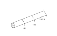
- the figure which shows the state which the crack produced in the wire material.
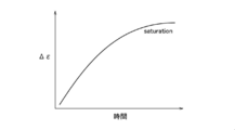
- the graph which shows that distortion amount is saturated with progress of time.
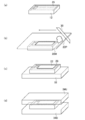
- It is a figure which shows the manufacturing method of the semiconductor device which concerns on 1st or 2nd embodiment, (a) The figure which shows a semiconductor chip, (b) The figure which shows a mask printing process, (c) The figure which shows a drying process, (D) The figure which shows a baking process.
- FIG. 2 is a schematic configuration diagram of a module using the semiconductor device according to the first embodiment.
- FIG. 7 is a temperature profile example in a thermal cycle test of the semiconductor device according to the first or second embodiment.
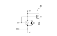
- 1 is a semiconductor device according to the first or second embodiment, and (a) a schematic circuit representation of a SiC MISFET of a one-in-one module (1 in 1 Module), and (b) a schematic of an IGBT of a one-in-one module. Circuit representation diagram.
- FIG. 4 is a detailed circuit representation diagram of the SiC MISFET of the one-in-one module, which is the semiconductor device according to the first or second embodiment.
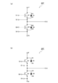
- FIG. 1 is a semiconductor device according to a first or second embodiment, wherein (a) a schematic circuit representation of a SiC MISFET of a two-in-one module, (b) an insulated gate bipolar transistor (IGBT: Insulated-Gate-Bipolar-Transistor) of the two-in-one module.
- IGBT Insulated-Gate-Bipolar-Transistor
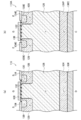
- FIG. 3 is a schematic cross-sectional structure diagram of a SiC MISFET that is an example of a semiconductor device applied to the semiconductor device according to the first or second embodiment and includes a source pad electrode SP and a gate pad electrode GP.
- FIG. 5 is a schematic cross-sectional structure diagram of an IGBT including an emitter pad electrode EP and a gate pad electrode GP, which is an example of a semiconductor device applied to the semiconductor device according to the first or second embodiment.
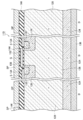
- FIG. 3 is a schematic cross-sectional structure diagram of a SiC DI (Double-Implanted) MISFET, which is an example of a semiconductor device applicable to the semiconductor device according to the first or second embodiment.
- FIG. 3 is a schematic cross-sectional structure diagram of a SiC trench (T: Trench) MISFET, which is an example of a semiconductor device applicable to the semiconductor device according to the first or second embodiment.
- T Trench
- MISFET SiC trench
- FIG. 3 A circuit configuration example in which an IGBT is applied as a semiconductor device and a snubber capacitor is connected between a power supply terminal PL and a ground terminal NL.
- the typical circuit block diagram of the three-phase alternating current inverter comprised using the semiconductor device which concerns on 1st or 2nd embodiment which applied SiC MISFET as a semiconductor device.
- the typical circuit block diagram of the three-phase alternating current inverter comprised using the semiconductor device which concerns on 1st or 2nd Embodiment which applied IGBT as a semiconductor device.
- FIG. 2 is a schematic bird's-eye view of the semiconductor device according to the first embodiment.
- the semiconductor device according to the first embodiment is a highly heat-resistant fired film 22 formed so as to cover the semiconductor chip 12 and the source pad electrode 14 on the semiconductor chip 12.
- the high heat resistant fired film 22 may be a silver fired film or a copper fired film.
- the silver fired film is referred to as “silver fired cap 22”
- the copper fired film is referred to as “copper fired cap 22”.
- the semiconductor chip 12 is disposed on the first substrate electrode 10B, and one end of the copper wire 18 is bonded onto the silver firing cap 22 by ultrasonic waves. Further, the other end of the copper wire 18 is joined to the second substrate electrode 20B by ultrasonic waves.
- an Al wire or a clad wire may be applied in place of the copper wire 18.
- the central part is made of Cu, but Al is joined so that the central part covers Cu.
- the clad wire has higher heat resistance and lower heat resistance than the Al wire.
- the first substrate electrode 10B and the second substrate electrode 20B are circuit boards made of a metal / ceramic / metal bonded body, such as a DBC (Direct Bonding Copper) substrate, a DBA (Direct Brazed Aluminum) substrate, or an AMB. (Active Metal Brazed, Active Metal Bond)
- a metal / ceramic / metal bonded body such as a DBC (Direct Bonding Copper) substrate, a DBA (Direct Brazed Aluminum) substrate, or an AMB.
- An insulating substrate such as a substrate may be used as a conductive pattern on the chip mounting surface side. Basically, the same metal materials are used for the front-side electrode and the back-side electrode of the insulating substrate.
- a Cu / Al 2 O 3 / Cu structure can be applied to a DBC substrate
- an Al / AlN / Al structure can be applied to a DBA substrate
- a Cu / Si 3 N 4 / Cu structure can be applied to an AMB substrate.
- the front surface side electrode serves as a positive (P) side power electrode, a negative (N) side power electrode, an output (Out) side power electrode, or the like by joining chips or electrodes or cutting patterns.
- the back surface side electrode has a role of transferring heat downward, such as being bonded to a cooler or bonded to a heat spreader.
- the semiconductor device employs a structure in which a cap is formed on the source pad electrode 14 on the semiconductor chip 12 with a high heat-resistant fired material (silver fired or copper fired).
- a high heat-resistant fired material silver fired or copper fired.
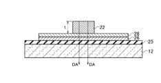
- FIG. 3 is a schematic cross-sectional structure diagram showing a simulation model of the semiconductor device according to the first embodiment.
- an oxide film 25 is formed on a silicon carbide (SiC) based semiconductor chip 12
- an aluminum electrode 26 is formed on the oxide film 25, and gold is formed on the aluminum electrode 26 by a plating process.
- An (Au) thin film 28 is formed, and a silver firing cap 22 is formed on the gold thin film 28.
- the aluminum electrode 26 is illustrated, but the material of the electrode is not limited to aluminum, and may be copper (Cu).
- the gold thin film 28 is for attaching the silver fired cap 22.
- a silver thin film or a palladium (Pd) thin film may be formed.
- FIG. 4 is a graph showing the effect of the simulation model shown in FIG.
- the horizontal axis indicates the film thickness t of the silver fired cap 22.
- the vertical axis represents the maximum principal stress ratio applied to the oxide film 25 when the displacement DA is applied to the silver firing cap 22.
- the stress applied to the oxide film 25 when the silver firing cap 22 is not provided is “1” (see point P1).
- the stress applied to the oxide film 25 can be dramatically reduced.
- the maximum principal stress ratio was about 0.4 (see point P2).
- the maximum principal stress ratio was about 0.2 (see point P3).
- the maximum principal stress ratio was about 0.1 (see point P4).
- the film thickness t of the silver firing cap 22 is not particularly limited, but is preferably about 10 ⁇ m to 100 ⁇ m, for example (see line Q).
- the electrodes on the device are capped using silver firing. Since this cap structure plays the role of a cushioning material, damage from the copper wire 18 can be reduced. Of course, if the copper wire 18 is used, very strong bonding is possible, and there is an effect that the power cycle resistance is increased.
- Pb-free solders 17A and 17B are used as the bonding material.
- the Pb-free solders 17A and 17B are Sn solders containing tin (Sn) as a main component and silver (Ag), copper (Cu), tin (Sn) and the like as additives.
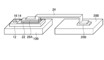
- FIG. 6 is a schematic bird's-eye view of the semiconductor device according to the second embodiment.
- the semiconductor device according to the second embodiment is formed so as to cover the semiconductor chip 12 and the source pad electrode 14 on the semiconductor chip 12 as in the first embodiment.
- the high heat resistant fired film 22 is a silver fired cap 22 (or copper fired cap 22).
- the film thickness t of the silver fired cap 22 is not particularly limited, but is preferably about 10 ⁇ m to 100 ⁇ m, for example.
- the semiconductor chip 12 is disposed on the first substrate electrode 10B, and one end of the flat upper wiring 24 is bonded onto the high heat resistant fired film 22 using the solder 26A as a bonding material. Further, the other end of the upper wiring 24 is joined to the second substrate electrode 20B using the solder 26B as a joining material.
- solders 26A and 26B Pb-free solder can be used as in the second comparative example.
- the source pad electrode 14 on the semiconductor chip 12 is capped with a high heat-resistant fired material (silver fired or copper fired), and a conventional solder is formed thereon. Like to use. Thereby, it is possible to reduce the cumulative equivalent strain applied to the solder and to improve the power cycle tolerance.
- a high heat-resistant fired material silver fired or copper fired
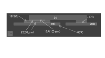
- FIG. 7 is a schematic sectional view showing a simulation model 1 (cap structure) of a semiconductor device according to the second embodiment.
- a Pb-free solder 17 ⁇ / b> A is used on the silver firing cap 22. It is assumed that the solder 17A, 17B has a film thickness of 100 ⁇ m, and the silver fired cap 22 has a film thickness of 50 ⁇ m. It is assumed that the back surface of the substrate electrode 10B is cooled at 65 ° C.
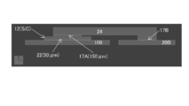
- FIG. 8 is a schematic sectional view showing a simulation model 2 (solder structure) of a semiconductor device according to Comparative Example 2. As shown in FIG. 8, in the simulation model 2, only Pb-free solders 17A and 17B are used. That is, the silver firing cap 22 is not disposed on the semiconductor chip 12 but is disposed only under the semiconductor chip 12. It is assumed that the film thickness of the solders 17A and 17B is 150 ⁇ m.
- FIG. 9 is a graph showing a comparison result between the simulation model 1 and the simulation model 2.
- the vertical axis represents the cumulative equivalent strain applied to the solder, and the horizontal axis represents the junction temperature Tj. Cumulative equivalent strain is used as a guide when estimating the life of a material such as solder. For the same material, the longer the cumulative equivalent strain, the shorter the life.
- a line segment S connecting the points S1 and S2 represents a change in accumulated equivalent strain in the simulation model 2 (solder structure). As can be seen from the line segment S, in the solder structure, the cumulative equivalent strain increases as the junction temperature Tj increases.
- a line segment C + S connecting the points C1 and C2 represents a change in accumulated equivalent strain in the simulation model 1 (cap structure).
- the cumulative equivalent strain hardly changes even if the junction temperature Tj changes due to the buffer effect of the silver fired cap 22.
- the cumulative equivalent strain is reduced by about 32% compared to the solder structure (see points C1 and S1). Further, it was found that when the junction temperature Tj is 200 ° C., the cumulative equivalent strain is reduced by about 44% (see points C2 and S2).
- the cap structure there is an effect that the power cycle tolerance can be improved, or even if the ⁇ Tj power cycle and MaxTj increase, the power cycle tolerance can be maintained.
- the ⁇ Tj power cycle is a difference between the maximum value MaxTj of the junction temperature Tj when the power cycle is turned on and the junction temperature MinTj when the power cycle is turned off, as shown in the following equation.
- MaxTj is 150 ° C. and MinTj is 50 ° C.
- the ⁇ Tj power cycle is 100 ° C.
- MaxTj is 200 ° C. and MinTj is 50 ° C.
- the ⁇ Tj power cycle is 150 ° C.
- the relationship between the ⁇ Tj power cycle and the power cycle life is schematically represented as shown in FIG. Normally, as shown in FIG. 10, when the ⁇ Tj power cycle is low, the lifetime tends to be long (see T1), and when the ⁇ Tj power cycle is high, the lifetime tends to be short (see T2). In addition, the wire material joined at a point tends to cause crack 18C (see FIG. 11), and the lead material joined at the surface tends to have a longer life.
- ⁇ ac_ne (fin_step) is the cumulative equivalent strain in the second cycle
- ⁇ ac_ne (ref_step) is the cumulative equivalent strain in the first cycle.
- the interval is between the first cycle and the second cycle.
- [Delta] [epsilon] P is smaller life extended. According to the cap structure, it can be seen that the cumulative equivalent strain is reduced, so that the life of the solder is extended.
- Pb-free solders 17A and 17B are used on the silver firing cap 22. Thereby, by buffering the stress directly received by the solder with the silver firing cap 22, it is possible to reduce the cumulative equivalent strain applied to the solder and to improve the power cycle tolerance.
- a gold thin film 28 is formed on the semiconductor chip 12.
- the baking paste 22 ⁇ / b> P is pushed in from the opening of the mask 28 ⁇ / b> M using the squeegee 30, and mask printing is performed on the region corresponding to the source pad electrode 14.
- the semiconductor chip 12 on which the baking paste 22 ⁇ / b> P is mask-printed is dried on a hot plate 32.
- the semiconductor chip 12 is baked (heat + pressurization) using the heating plates 34U, 34D. Thereby, as shown in FIG. 14, the silver firing cap 22 can be formed on the upper portion of the semiconductor chip 12.
- a dispensing method may be applied instead of mask printing. Even if the dispensing method is used, a fired film having the same quality can be produced.
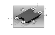
- FIG. 15 is a configuration diagram (photograph) of a module using the semiconductor device according to the second embodiment, where (a) is a bird's-eye view and (b) is a plan view.
- the first substrate electrode 10 ⁇ / b> B and the second substrate electrode 20 ⁇ / b> B are connected by the upper wiring 24.
- the signal electrode terminals G1, D1, S1 and the signal electrode terminals G4, D4, S4 are led out from the first substrate electrode 10B and the second substrate electrode 20B, respectively.
- substrate electrodes other than the first substrate electrode 10B and the second substrate electrode 20B can be connected by the upper wiring 24.
- the substrate electrode 10B is connected to a power terminal P corresponding to the drain D1 of the high level MISFET Q1, and the substrate electrode 20B is connected to the drain D4 of the low level MISFET Q4 or the source S1 of the high level MISFET Q1.
- the corresponding power terminal O (output terminal) is connected.
- a power terminal N corresponding to the source S4 of the low-level MISFET Q4 is connected to the land electrode connected to the source pad electrode S1 of the low-level MISFET Q1 via the upper wiring 24.
- the MISFET Q1 on the high level side and the MISFET Q4 on the low level side correspond to, for example, semiconductor devices constituting a two-in-one module circuit as shown in FIG. Note that IGBTs Q1 and Q4 of a two-in-one module as shown in FIG. The same applies hereinafter.
- FIG. 16 is a configuration diagram (photograph) after the module shown in FIG. 15 is molded.
- the first substrate electrode 10B and the second substrate electrode 20B are formed of resin M or the like.
- FIGS. 17 and 18 are photographs in which the module shown in FIG. 15 is partially enlarged.
- the semiconductor chip 12 is disposed on the first substrate electrode 10B.
- a silver firing cap 22 is formed on the semiconductor chip 12, and the upper wiring 24 is joined onto the silver firing cap 22 using solders 26 ⁇ / b> A and 26 ⁇ / b> B.
- FIG. 19 is a photograph showing the entire module shown in FIG.
- FIG. 20 is a partially enlarged photograph of the module shown in FIG.
- the semiconductor chip 12 is connected to the signal electrode terminals G1, D1, S1 and the signal electrode terminals G4, D4, S4 via the wires W.
- FIG. 21 is a schematic configuration diagram of a module using the semiconductor device according to the first embodiment. As shown in FIG. 21, a plurality of copper wires 18 can be bonded to one semiconductor chip 12.
- the joining energy is obtained by integrating the friction coefficient ⁇ , speed v, and pressure P at the time of joining as shown in the following equation. Both the coefficient of friction ⁇ and the speed v are functions of the pressure P. Generally, the higher the bonding energy, the higher the bonding force.
- the ⁇ Tj power cycle test is a test for raising and lowering the bonding temperature in a relatively short period as shown in FIG. 22, and for example, it is possible to evaluate the life of the wire bonding portion and the like.
- the semiconductor device module is repeatedly energized and interrupted to heat the chip.
- Tj 150 ° C. for 2 s
- Thermal cycle test In the semiconductor device according to the first or second embodiment, an example of a temperature profile in the thermal cycle test is expressed as shown in FIG.
- the thermal cycle test was performed in an air atmosphere and was performed in the range of minus 40 ° C. to plus 150 ° C.
- the cycle of one thermal cycle is 80 minutes, and the breakdown is as follows: minus 40 ° C. for 30 minutes, minus 40 ° C. to plus 150 ° C. for 10 minutes, plus 150 ° C. for 30 minutes, plus 150 ° C.
- the cooling time to minus 40 ° C. is 10 minutes.
- the forward voltage drop Vf and the reverse withstand voltage Vr were measured every 100 cycles, but no characteristic deterioration was observed.
- the resistance increases and the forward voltage Vf changes in the test in which a high current such as the forward direction flows. Even if the power cycle tolerance occurs including the characteristic degradation, if the progress of the degradation is slow, it can be evaluated that the power cycle tolerance is high.
- the copper wire 18 or the solder 26A is disposed on the silver fired cap 22, but the present invention is not limited to this.
- the upper wiring 24 may be bonded onto the silver firing cap 22 by silver firing.
- the film thickness can be increased by firing silver on the silver firing cap 22. As a result, higher heat resistance than that of the solder 26A can be achieved, and the reliability can be improved.
- FIG. 24A shows a diode DI connected in antiparallel to the MISFETQ.
- the main electrode of the MISFET Q is represented by a drain terminal DT and a source terminal ST.
- FIG. 24B shows a diode DI connected in reverse parallel to the IGBTQ.
- the main electrode of the IGBTQ is represented by a collector terminal CT and an emitter terminal ET.
- a fast recovery diode (FRD) or a Schottky barrier diode (SBD) may be externally attached.
- FBD fast recovery diode
- SBD Schottky barrier diode
- MISFETs may be built in one module.
- five chips (MISFET ⁇ 5) can be mounted, and up to five MISFETs Q can be connected in parallel. A part of the five chips can be mounted for the diode DI.
- a sense MISFET Qs is connected in parallel to the MISFET Q.
- the sense MISFET Qs is formed as a fine transistor in the same chip as the MISFET Q.
- SS is a source sense terminal
- CS is a current sense terminal
- G is a gate signal terminal.
- the sense MISFET Qs is formed as a fine transistor in the same chip.
- G1 is a gate signal terminal of the MISFET Q1
- S1 is a source terminal of the MISFET Q1.
- G4 is a gate signal terminal of the MISFET Q4, and S4 is a source terminal of the MISFET Q4.
- P is a positive power input terminal
- N is a negative power input terminal
- O is an output terminal.
- FIG. 26B a schematic circuit expression of the IGBT of the two-in-one module is expressed as shown in FIG.
- FIG. 26B two IGBTs Q1 and Q4 and diodes D1 and D4 connected in reverse parallel to the IGBTs Q1 and Q4 are built in one module.
- G1 is a gate signal terminal of the IGBT Q1
- E1 is an emitter terminal of the IGBT Q1.
- G4 is a gate signal terminal of the IGBT Q4, and E4 is an emitter terminal of the IGBT Q4.
- P is a positive power input terminal
- N is a negative power input terminal
- O an output terminal.
- Typical cross-sectional structure of SiC MISFET is represented as shown to Fig.27 (a)
- Typical cross-sectional structure of IGBT is It is expressed as shown in FIG.
- a schematic cross-sectional structure of a SiC MISFET is a semiconductor composed of an n ⁇ high resistance layer as shown in FIG.
- the substrate 126, the p body region 128 formed on the surface side of the semiconductor substrate 126, the source region 130 formed on the surface of the p body region 128, and the surface of the semiconductor substrate 126 between the p body regions 128 are disposed.
- N + drain region 124 and drain electrode 136 connected to n + drain region 124.
- the semiconductor device 110 is composed of a planar gate type n-channel vertical SiC MISFET. However, as shown in FIG. 31 to be described later, the semiconductor device 110 may be composed of an n-channel vertical SiC TMISFET or the like. good.
- GaN-based FET or the like may be employed instead of the SiC MISFET for the semiconductor device 110 (Q) applicable to the first or second embodiment.
- the semiconductor device 110 applicable to the first or second embodiment either a SiC-based power device or a GaN-based power device can be adopted.
- a semiconductor called a wide gap type having a band gap energy of, for example, 1.1 eV to 8 eV can be used.
- the IGBT includes a semiconductor substrate 126 made of an n ⁇ high resistance layer, and P body region 128 formed on the surface side of semiconductor substrate 126, emitter region 130E formed on the surface of p body region 128, and gate insulation disposed on the surface of semiconductor substrate 126 between p body regions 128 Film 132, gate electrode 138 disposed on gate insulating film 132, emitter electrode 134E connected to emitter region 130E and p body region 128, and p disposed on the back surface opposite to the surface of semiconductor substrate 126 + Collector region 124P and collector electrode 136C connected to p + collector region 124P.
- the semiconductor device 110A is composed of a planar gate type n-channel vertical IGBT, but may be composed of a trench gate type n-channel vertical IGBT or the like.
- FIG. 28 is an example of the semiconductor device 110 applicable to the first or second embodiment, and a schematic cross-sectional structure of an SiC MISFET including the source pad electrode SP and the gate pad electrode GP is expressed as shown in FIG.
- the Gate pad electrode GP is connected to gate electrode 138 arranged on gate insulating film 132, and source pad electrode SP is connected to source electrode 134 connected to source region 130 and p body region 128.
- the gate pad electrode GP and the source pad electrode SP are disposed on a passivation interlayer insulating film 144 that covers the surface of the semiconductor device 110. Note that a fine transistor structure may be formed in the semiconductor substrate 126 below the gate pad electrode GP and the source pad electrode SP, as in the central portion of FIG.
- the source pad electrode SP may be extended and disposed on the passivation interlayer insulating film 144.
- Gate pad electrode GP is connected to gate electrode 138 disposed on gate insulating film 132, and emitter pad electrode EP is connected to emitter region 134E and emitter electrode 134E connected to p body region 128.
- the gate pad electrode GP and the emitter pad electrode EP are disposed on a passivation interlayer insulating film 144 covering the surface of the semiconductor device 110A.
- a fine IGBT structure may be formed in the semiconductor substrate 126 below the gate pad electrode GP and the emitter pad electrode EP, as in the central portion of FIG. 27B or FIG.
- the emitter pad electrode EP may be arranged to extend on the interlayer insulating film 144 for passivation.
- SiC DMISFET- It is an example of the semiconductor device 110 applicable to 1st or 2nd embodiment, Comprising: The typical cross-section of SiC DISMISFET is represented as shown in FIG.
- the SiC DISMISFET applicable to the first or second embodiment includes a semiconductor substrate 126 made of an n ⁇ high resistance layer and a p body region 128 formed on the surface side of the semiconductor substrate 126.
- source electrode 134 connected to source region 130 and p body region 128, n + drain region 124 disposed on the back surface opposite to the surface of semiconductor substrate 126, and n + drain region 124
- the drain electrode 136 is provided.
- a p body region 128 and an n + source region 130 formed on the surface of the p body region 128 are formed by double ion implantation (DI). 130 and source electrode 134 connected to p body region 128.
- the gate pad electrode GP (not shown) is connected to the gate electrode 138 disposed on the gate insulating film 132. Further, as shown in FIG. 30, the source pad electrode SP and the gate pad electrode GP (not shown) are disposed on a passivation interlayer insulating film 144 that covers the surface of the semiconductor device 110.
- a depletion layer as shown by a broken line is formed in a semiconductor substrate 126 made of an n ⁇ high resistance layer sandwiched between p body regions 128, a junction type FET ( A channel resistance R JFET due to the JFET) effect is formed.
- a body diode BD is formed between the p body region 128 and the semiconductor substrate 126 as shown in FIG.
- SiC TMISFET It is an example of the semiconductor device 110 applicable to 1st or 2nd embodiment, Comprising: The typical cross-section of SiC TMISFET is represented as shown in FIG.
- the SiC TMISFET applicable to the first or second embodiment includes an n-layer semiconductor substrate 126N, a p body region 128 formed on the surface side of the semiconductor substrate 126N, and a p-type region. Formed in the trench formed through the n + source region 130 and the p body region 128 formed on the surface of the body region 128 and up to the semiconductor substrate 126N through the gate insulating layer 132 and the interlayer insulating films 144U and 144B.
- Trench gate electrode 138TG source electrode 134 connected to source region 130 and p body region 128, n + drain region 124 disposed on the back surface opposite to the surface of semiconductor substrate 126N, and n + drain region And a drain electrode 136 connected to 124.
- a trench gate electrode 138TG formed through a gate insulating layer 132 and interlayer insulating films 144U and 144B is formed in a trench penetrating the p body region 128 and extending to the semiconductor substrate 126N.
- the source pad electrode SP is connected to the source electrode 134 connected to the source region 130 and the p body region 128.
- the gate pad electrode GP (not shown) is connected to the gate electrode 138 disposed on the gate insulating film 132. Further, as shown in FIG. 31, the source pad electrode SP and the gate pad electrode GP (not shown) are arranged on a passivation interlayer insulating film 144U that covers the surface of the semiconductor device 110.
- the channel resistance R JFET associated with the junction FET (JFET) effect like the SiC DIMISFET is not formed.
- a body diode BD is formed between the p body region 128 and the semiconductor substrate 126N.
- a SiC MISFET is applied as a semiconductor device, and a snubber capacitor is connected between the power supply terminal PL and the ground terminal NL.
- a circuit configuration example in which C is connected is expressed as shown in FIG.
- an IGBT is applied as a semiconductor device, and between the power supply terminal PL and the ground terminal NL.
- a circuit configuration example to which the snubber capacitor C is connected is expressed as shown in FIG.
- a large surge voltage Ldi / dt is generated due to the high switching speed of the SiC MISFET and IGBT due to the inductance L of the connection line.
- di / dt 3 ⁇ 10 9 (A / s).
- the value of the surge voltage Ldi / dt varies depending on the value of the inductance L, the surge voltage Ldi / dt is superimposed on the power supply V.
- the surge voltage Ldi / dt can be absorbed by the snubber capacitor C connected between the power supply terminal PL and the ground terminal NL.
- the three-phase AC inverter 140 includes a gate drive unit 150, a semiconductor device unit 152 connected to the gate drive unit 150, and a three-phase AC motor unit 154.
- the semiconductor device unit 152 is connected to U-phase, V-phase, and W-phase inverters corresponding to the U-phase, V-phase, and W-phase of the three-phase AC motor unit 154.
- the gate drive unit 150 is connected to the SiC MISFETs Q1 and Q4, the SiC MISFETs Q2 and Q5, and the SiC MISFETs Q3 and Q6.
- the semiconductor device section 152 is connected between the plus terminal (+) and minus terminal ( ⁇ ) of the converter 148 to which the storage battery (E) 146 is connected, and the SiC MISFETs Q1 and Q4, Q2 and Q5, and Q3 and Q6 having inverter configurations are connected. Is provided. Free wheel diodes D1 to D6 are connected in antiparallel between the sources and drains of the SiC MISFETs Q1 to Q6, respectively.
- the three-phase AC inverter 140A includes a gate drive unit 150A, a semiconductor device unit 152A connected to the gate drive unit 150A, and a three-phase AC motor unit 154A.
- the semiconductor device unit 152A is connected to U-phase, V-phase, and W-phase inverters corresponding to the U-phase, V-phase, and W-phase of the three-phase AC motor unit 154A.
- the gate drive unit 150A is connected to the IGBTs Q1 and Q4, the IGBTs Q2 and Q5, and the IGBTs Q3 and Q6.
- the semiconductor device portion 152A is connected between the plus terminal (+) and minus terminal ( ⁇ ) of the converter 148A to which the storage battery (E) 146A is connected, and the IGBTs Q1 ⁇ Q4, Q2 ⁇ Q5, and Q3 ⁇ Q6 of the inverter configuration are connected. Prepare. Furthermore, free wheel diodes D1 to D6 are connected in antiparallel between the emitters and collectors of IGBTs Q1 to Q6, respectively.
- the semiconductor device or power module according to this embodiment can be formed in any one of one-in-one, two-in-one, four-in-one, six-in-one, or seven-in-one types.
- the semiconductor device and power module of the present embodiment can be used for semiconductor module manufacturing technology such as IGBT module, diode module, MOS module (Si, SiC, GaN), inverter for HEV / EV, and industrial equipment It can be applied to a wide range of application fields such as inverters and converters.
- semiconductor module manufacturing technology such as IGBT module, diode module, MOS module (Si, SiC, GaN), inverter for HEV / EV, and industrial equipment It can be applied to a wide range of application fields such as inverters and converters.
Landscapes
- Engineering & Computer Science (AREA)
- Wire Bonding (AREA)
- Manufacturing & Machinery (AREA)
- Chemical & Material Sciences (AREA)
- Ceramic Engineering (AREA)
- Electrodes Of Semiconductors (AREA)
- Internal Circuitry In Semiconductor Integrated Circuit Devices (AREA)
- Cooling Or The Like Of Semiconductors Or Solid State Devices (AREA)
- Inverter Devices (AREA)
Abstract
半導体装置は、半導体チップ(12)と、半導体チップ(12)上のソースパッド電極(14)を覆うように形成される銀焼成キャップ(22)とを備える。半導体チップ(12)が第1の基板電極(10B)上に配置され、超音波により銀焼成キャップ(22)上に銅ワイヤ(18)の一方端が接合される。パワーサイクル耐量を向上させることが可能な半導体装置、パワーモジュール及びその製造方法を提供する。
Description
本実施の形態は、半導体装置、パワーモジュール及びその製造方法に関する。
パワーモジュールのジャンクション温度Tjの上昇とともに、パワーサイクル耐量が従来の技術(アルミワイヤ)では厳しくなっている。そこで、最近では、寿命を延ばすためにアルミワイヤではなく銅ワイヤを使用する場合がある。また、ワイヤに代えてリード材や電極柱などの上部配線を使用する場合もある。
しかし、銅ワイヤを半導体チップ上に接合する場合は、アルミワイヤに比べ超音波のパワーが非常に大きくなるため、デバイスを破壊してしまう。
また、リード材や電極柱などの上部配線を使用する場合は、その接合材としてPbフリー系のはんだが使用される。しかし、Pbフリー系のはんだを使用した場合、シリコンカーバイド(SiC)など200℃以上の耐熱性を持つデバイスでは、融点がジャンクション温度Tj=200℃に近く、さらにΔTjパワーサイクルが大きくなるため、パワーサイクル耐量(パワーサイクル寿命)は小さくなってしまう。
本実施の形態は、パワーサイクル耐量を向上させることが可能な半導体装置、パワーモジュール及びその製造方法を提供する。
本実施の形態の一態様によれば、半導体チップと、前記半導体チップ上の電極を覆うように形成される高耐熱性の焼成膜とを備える半導体装置が提供される。
本実施の形態の他の態様によれば、半導体チップが形成される工程と、前記半導体チップ上の電極を覆うように高耐熱性の焼成膜が形成される工程とを有する半導体装置の製造方法が提供される。
本実施の形態によれば、パワーサイクル耐量を向上させることが可能な半導体装置、パワーモジュール及びその製造方法を提供することができる。
次に、図面を参照して、実施の形態を説明する。以下の図面の記載において、同一又は類似の部分には同一又は類似の符号を付している。ただし、図面は模式的なものであり、厚みと平面寸法との関係、各層の厚みの比率等は現実のものとは異なることに留意すべきである。したがって、具体的な厚みや寸法は以下の説明を参酌して判断すべきものである。又、図面相互間においても互いの寸法の関係や比率が異なる部分が含まれていることはもちろんである。
又、以下に示す実施の形態は、技術的思想を具体化するための装置や方法を例示するものであって、構成部品の材質、形状、構造、配置等を下記のものに特定するものでない。この実施の形態は、特許請求の範囲において、種々の変更を加えることができる。
[比較例1]
既に説明したように、パワーモジュールのジャンクション温度Tjの上昇とともに、パワーサイクル耐量がアルミワイヤでは厳しくなっている。そこで、比較例1に係る半導体装置では、図1に示すように、銅ワイヤ18を使用して第1の基板電極10Bと第2の基板電極20Bとを接続している。具体的には、第1の基板電極10B上に半導体チップ12を配置し、半導体チップ12上のソースパッド電極14の所定位置18Bに超音波を印加し、銅ワイヤ18を接合している。符号16はゲートパッド電極である。
既に説明したように、パワーモジュールのジャンクション温度Tjの上昇とともに、パワーサイクル耐量がアルミワイヤでは厳しくなっている。そこで、比較例1に係る半導体装置では、図1に示すように、銅ワイヤ18を使用して第1の基板電極10Bと第2の基板電極20Bとを接続している。具体的には、第1の基板電極10B上に半導体チップ12を配置し、半導体チップ12上のソースパッド電極14の所定位置18Bに超音波を印加し、銅ワイヤ18を接合している。符号16はゲートパッド電極である。
しかし、比較例1に係る半導体装置によると、銅ワイヤ18を接合する際に非常に大きな超音波のパワーが必要になり、デバイスを破壊してしまう。もしくは、破壊を防ぐためのパッドの構造を作成する必要があり、デバイス構造が複雑化してしまう。
[第1の実施の形態]
(半導体装置)
図2は、第1の実施の形態に係る半導体装置の模式的鳥瞰図である。
(半導体装置)
図2は、第1の実施の形態に係る半導体装置の模式的鳥瞰図である。
図2(a)に示すように、第1の実施の形態に係る半導体装置は、半導体チップ12と、半導体チップ12上のソースパッド電極14を覆うように形成される高耐熱性の焼成膜22とを備える。
例えば、高耐熱性の焼成膜22は、銀焼成膜でもよいし、銅焼成膜でもよい。以下、銀焼成膜を「銀焼成キャップ22」、銅焼成膜を「銅焼成キャップ22」という。
図2(b)に示すように、半導体チップ12が第1の基板電極10B上に配置され、超音波により銀焼成キャップ22上に銅ワイヤ18の一方端が接合される。また、超音波により銅ワイヤ18の他方端が第2の基板電極20Bに接合される。
尚、銅ワイヤ18の代わりに、Alワイヤやクラッドワイヤを適用しても良い。クラッドワイヤにおいては、中心部はCuで形成されているが、中心部はCuを覆うようにAlが接合されている。クラッドワイヤは、Alワイヤに比べ高耐熱性・低熱抵抗性を有している。
ここで、第1の基板電極10Bや第2の基板電極20Bは、金属とセラミックスと金属との接合体からなる回路基板、例えばDBC(Direct Bonding Copper)基板、DBA(Direct Brazed Aluminum)基板やAMB(Active Metal Brazed, Active Metal Bond)基板などの絶縁基板(回路基板)の、チップ搭載面側の導体パターンにより構成することもできる。絶縁基板の表面側電極および裏面側電極の金属材料としては基本的には同じものが使われる。例えば、DBC基板であれば、Cu/Al2O3/Cu構造、DBA基板であれば、Al/AlN/Al構造、AMB基板であれば、Cu/Si3N4/Cu構造などを適用可能である。ただし、表面側電極および裏面側電極では役割が多少異なる。表面側電極は、チップや電極などを接合したり、それぞれパターンを切り、正(P)側パワー電極、負(N)側パワー電極、出力(Out)側パワー電極などの役目を果たす。裏面側電極は、冷却器へ接合されたり、ヒートスプレッダに接合したりと熱を下に伝える役目を有する。
以上のように、第1の実施の形態に係る半導体装置では、半導体チップ12上のソースパッド電極14上に高耐熱焼成材料(銀焼成又は銅焼成)でキャップを行う構造を採用している。これにより、銅ワイヤ接合時にかかる超音波のパワーが緩衝され、銅ワイヤ接合時にかかる大きな荷重からデバイスの破壊を防ぐことができるため、パワーサイクル耐量を向上させることが可能となる。
(銀焼成キャップによるデバイスへのダメージの低減効果)
図3は、第1の実施の形態に係る半導体装置のシミュレーションモデルを示す模式的断面構造図である。ここでは、図3に示すように、シリコンカーバイド(SiC)ベースの半導体チップ12上に酸化膜25が形成され、酸化膜25上にアルミニウム電極26が形成され、アルミニウム電極26上にメッキ工程で金(Au)薄膜28が形成され、金薄膜28上に銀焼成キャップ22が形成されている。
図3は、第1の実施の形態に係る半導体装置のシミュレーションモデルを示す模式的断面構造図である。ここでは、図3に示すように、シリコンカーバイド(SiC)ベースの半導体チップ12上に酸化膜25が形成され、酸化膜25上にアルミニウム電極26が形成され、アルミニウム電極26上にメッキ工程で金(Au)薄膜28が形成され、金薄膜28上に銀焼成キャップ22が形成されている。
ここでは、アルミニウム電極26を例示しているが、電極の材料はアルミニウムに限定されるものではなく、銅(Cu)でもよい。
また、金薄膜28は、銀焼成キャップ22を付着させるためのものである。金薄膜28に代えて、銀薄膜、又はパラジウム(Pd)薄膜を形成してもよい。
図4は、図3に示されるシミュレーションモデルの効果を示すグラフである。横軸は、銀焼成キャップ22の膜厚tを示す。縦軸は、銀焼成キャップ22に変位DAを与えた際に酸化膜25にかかる最大主応力比を示す。ここでは、銀焼成キャップ22がない場合の酸化膜25にかかる応力を「1」としている(点P1参照)。
図4に示される矢印Pを見ても分かるように、銀焼成キャップ22がある場合は、劇的に酸化膜25にかかる応力を低減できる。具体的には、銀焼成キャップ22の膜厚tが5μmである場合、最大主応力比は約0.4程度であった(点P2参照)。銀焼成キャップ22の膜厚tが10μmである場合、最大主応力比は約0.2程度であった(点P3参照)。銀焼成キャップ22の膜厚tが30μmである場合、最大主応力比は約0.1程度であった(点P4参照)。銀焼成キャップ22の膜厚tは特に限定されるものではないが、例えば、約10μm~100μm程度であるのが望ましい(線Q参照)。
以上のように、第1の実施の形態に係る半導体装置では、デバイス上の電極に銀焼成を用いてキャップを行うようにしている。このキャップ構造は、緩衝材の役割を果たすため、銅ワイヤ18からのダメージを低減することが可能となる。もちろん、銅ワイヤ18を使用すれば、非常に強い接合が可能になり、パワーサイクル耐量が増加するという効果もある。
[比較例2]
既に説明したように、パワーモジュールのジャンクション温度Tjの上昇とともに、パワーサイクル耐量がアルミワイヤでは厳しくなっている。そこで、比較例2に係る半導体装置では、図5に示すように、リード材や電極柱などの上部配線24を使用して第1の基板電極10Bと第2の基板電極20Bとを接続している。
既に説明したように、パワーモジュールのジャンクション温度Tjの上昇とともに、パワーサイクル耐量がアルミワイヤでは厳しくなっている。そこで、比較例2に係る半導体装置では、図5に示すように、リード材や電極柱などの上部配線24を使用して第1の基板電極10Bと第2の基板電極20Bとを接続している。
このようにリード材や電極柱などの上部配線24を使用する場合は、その接合材としてPbフリー系のはんだ17A,17Bが使用される。Pbフリー系のはんだ17A,17Bとは、スズ(Sn)を主成分として、銀(Ag)、銅(Cu)、スズ(Sn)などが添加物として配合されているSn系のはんだである。しかし、Pbフリー系のはんだ17A,17Bを使用した場合、シリコンカーバイド(SiC)など200℃以上の耐熱性を持つデバイスでは、融点がジャンクション温度Tj=200℃に近く、さらにΔTjパワーサイクルが大きくなるため、パワーサイクル耐量は小さくなってしまう。
[第2の実施の形態]
(半導体装置)
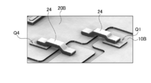
図6は、第2の実施の形態に係る半導体装置の模式的鳥瞰図である。
(半導体装置)
図6は、第2の実施の形態に係る半導体装置の模式的鳥瞰図である。
図6に示すように、第2の実施の形態に係る半導体装置は、第1の実施の形態と同様、半導体チップ12と、半導体チップ12上のソースパッド電極14を覆うように形成される高耐熱性の焼成膜22とを備える。
第1の実施の形態と同様、高耐熱性の焼成膜22は、銀焼成キャップ22(又は銅焼成キャップ22)である。銀焼成キャップ22の膜厚tは特に限定されるものではないが、例えば、約10μm~100μm程度であるのが望ましい。
半導体チップ12が第1の基板電極10B上に配置され、はんだ26Aを接合材として高耐熱性の焼成膜22上に平板状の上部配線24の一方端が接合される。また、はんだ26Bを接合材として上部配線24の他方端が第2の基板電極20Bに接合される。はんだ26A,26Bには、比較例2と同様、Pbフリー系のはんだを用いることができる。
以上のように、第2の実施の形態に係る半導体装置では、半導体チップ12上のソースパッド電極14上に高耐熱焼成材料(銀焼成又は銅焼成)でキャップを行い、その上に従来のはんだを使用するようにしている。これにより、はんだにかかる累積相当ひずみを減少させ、パワーサイクル耐量を向上させることが可能となる。
(銀焼成キャップ有無での累積相当ひずみの比較)
図7は、第2の実施の形態に係る半導体装置のシミュレーションモデル1(キャップ構造)を示す模式的断面構造図である。図7に示すように、シミュレーションモデル1では、Pbフリー系のはんだ17Aを銀焼成キャップ22上に使用している。はんだ17A,17Bの膜厚は100μmであり、銀焼成キャップ22の膜厚は50μmである場合を想定している。基板電極10Bの裏面は、65℃で冷却されることを想定している。
図7は、第2の実施の形態に係る半導体装置のシミュレーションモデル1(キャップ構造)を示す模式的断面構造図である。図7に示すように、シミュレーションモデル1では、Pbフリー系のはんだ17Aを銀焼成キャップ22上に使用している。はんだ17A,17Bの膜厚は100μmであり、銀焼成キャップ22の膜厚は50μmである場合を想定している。基板電極10Bの裏面は、65℃で冷却されることを想定している。
図8は、比較例2に係る半導体装置のシミュレーションモデル2(はんだ構造)を示す模式的断面構造図である。図8に示すように、シミュレーションモデル2では、Pbフリー系のはんだ17A,17Bのみを使用している。すなわち、銀焼成キャップ22は、半導体チップ12上には配置されておらず、半導体チップ12下にのみ配置されている。はんだ17A,17Bの膜厚は150μmである場合を想定している。
図9は、シミュレーションモデル1とシミュレーションモデル2の比較結果を示すグラフである。縦軸は、はんだにかかる累積相当ひずみを示し、横軸は、ジャンクション温度Tjを示す。累積相当ひずみは、はんだなどの材料の寿命を推定する際の目安として使用される。同じ材料では、累積相当ひずみが大きいほど寿命が短くなる。
点S1と点S2とを結ぶ線分Sは、シミュレーションモデル2(はんだ構造)における累積相当ひずみの変化を表している。線分Sを見ても分かるように、はんだ構造では、ジャンクション温度Tjの上昇とともに累積相当ひずみが大きくなる。
一方、点C1と点C2とを結ぶ線分C+Sは、シミュレーションモデル1(キャップ構造)における累積相当ひずみの変化を表している。線分C+Sを見ても分かるように、キャップ構造では、銀焼成キャップ22の緩衝効果により、ジャンクション温度Tjが変わっても累積相当ひずみはほとんど変化しない。
具体的には、キャップ構造によれば、はんだ構造に比べて、ジャンクション温度Tjが120℃である場合、累積相当ひずみは約32%程度減少することが分かった(点C1,点S1参照)。また、ジャンクション温度Tjが200℃である場合、累積相当ひずみは約44%程度減少することが分かった(点C2,点S2参照)。
以上のように、キャップ構造によれば、パワーサイクル耐量を向上できる、もしくはΔTjパワーサイクル、MaxTjが大きくなってもパワーサイクル耐量を保持できる効果がある。
ここで、ΔTjパワーサイクルは、次式に示すように、パワーサイクルをオンしたときのジャンクション温度Tjの最大値MaxTjとオフしたときのジャンクション温度MinTjとの差である。MaxTjが150℃でMinTjが50℃である場合、ΔTjパワーサイクルは100℃となり、MaxTjが200℃でMinTjが50℃である場合、ΔTjパワーサイクルは150℃となる。

ΔTjパワーサイクルとパワーサイクル寿命の関係は、模式的に図10に示すように表される。通常、図10に示すように、ΔTjパワーサイクルが低いときは寿命が長くなる傾向が見られ(T1参照)、ΔTjパワーサイクルが高いときは寿命が短くなる傾向が見られる(T2参照)。また、点で接合するワイヤ材は亀裂18Cが生じやすく(図11参照)、面で接合するリード材の方が寿命が長い傾向がある。
(はんだの寿命と累積相当ひずみの関係)
次に、疲労寿命の算出方法について説明する。非弾性ひずみ(塑性ひずみ、クリープひずみ)が発生するような大きな負荷を繰り返しかけて、少ない繰り返し数(105サイクル以下)で疲労破壊させる場合を低サイクル疲労と呼ぶ。低サイクル疲労の疲労寿命は以下に示すマンソン・コフィン則で表される。
次に、疲労寿命の算出方法について説明する。非弾性ひずみ(塑性ひずみ、クリープひずみ)が発生するような大きな負荷を繰り返しかけて、少ない繰り返し数(105サイクル以下)で疲労破壊させる場合を低サイクル疲労と呼ぶ。低サイクル疲労の疲労寿命は以下に示すマンソン・コフィン則で表される。

ΔεPは塑性ひずみ振幅[-]であり、Njは塑性疲労(疲労寿命)[回]であり、C,Nは材料物性値である。

εac_ne(fin_step)は2サイクル目の累積相当ひずみであり、εac_ne(ref_step)は1サイクル目の累積相当ひずみである。図12に示すように、時間の経過とともにひずみ量は飽和するため、数3では、1サイクル目と2サイクル目の間をとるようにしている。マンソン・コフィン則によれば、ΔεPが小さいと寿命は延びる。キャップ構造によれば、累積相当ひずみが小さくなるため、はんだの寿命が延びることが分かる。
以上のように、第2の実施の形態に係る半導体装置では、Pbフリー系のはんだ17A,17Bを銀焼成キャップ22上に使用するようにしている。これにより、はんだが直接受けていた応力を銀焼成キャップ22で緩衝することにより、はんだにかかる累積相当ひずみを減少させ、パワーサイクル耐量を向上させることが可能となる。
[製造方法]
以下、第1又は第2の実施の形態に係る半導体装置の製造方法について説明する。
以下、第1又は第2の実施の形態に係る半導体装置の製造方法について説明する。
まず、図13(a)に示すように、半導体チップ12の上部に金薄膜28を形成する。次いで、図13(b)に示すように、スキージ30を用いてマスク28Mの開口部から焼成ペースト22Pを押し込み、ソースパッド電極14に対応する領域にマスク印刷を行う。次いで、図13(c)に示すように、焼成ペースト22Pがマスク印刷された半導体チップ12をホットプレート32の上で乾燥させる。最後に、図13(d)に示すように、加熱プレート34U,34Dを用いて半導体チップ12を焼成(熱+加圧)する。これにより、図14に示すように、半導体チップ12の上部に銀焼成キャップ22を形成することができる。
尚、上記の工程において、マスク印刷の代わりに、ディスペンス法を適用しても良い。ディスペンス法を用いても同程度の品質の焼成膜を作成可能である。
[モジュール]
以下、第1又は第2の実施の形態に係る半導体装置を複数個備えるパワーモジュールの構成について説明する。
以下、第1又は第2の実施の形態に係る半導体装置を複数個備えるパワーモジュールの構成について説明する。
図15は、第2の実施の形態に係る半導体装置を用いたモジュールの構成図(写真)であり、(a)は鳥瞰図、(b)は平面図である。図15に示すように、第1の基板電極10Bと第2の基板電極20Bとが上部配線24により接続されている。第1の基板電極10Bと第2の基板電極20Bのそれぞれから外方に信号電極端子G1,D1,S1、信号電極端子G4,D4,S4が引き出されている。もちろん、第1の基板電極10Bと第2の基板電極20B以外の基板電極を上部配線24により接続することも可能である。また、基板電極10Bには、ハイレベル側のMISFETQ1のドレインD1に対応するパワー端子Pが接続され、基板電極20Bには、ローレベル側のMISFETQ4のドレインD4若しくはハイレベル側のMISFETQ1のソースS1に対応するに対応するパワー端子O(出力端子)が接続される。さらに、ローレベル側のMISFETQ1のソースパッド電極S1に上部配線24を介して接続されるランド電極には、ローレベル側のMISFETQ4のソースS4に対応するパワー端子Nが接続される。以上の説明において、ハイレベル側のMISFETQ1およびローレベル側のMISFETQ4は、例えば、図26(a)に示すようなツーインワンモジュールの回路を構成する半導体デバイスの対応している。尚、図26(b)に示すようなツーインワンモジュールのIGBT Q1・Q4であっても良い。以下同様である。
図16は、図15に示されるモジュールを成形した後の構成図(写真)である。図16に示すように、第1の基板電極10Bや第2の基板電極20Bは樹脂Mなどで成形される。
図17及び図18は、図15に示されるモジュールを部分的に拡大した写真である。図17及び図18に示すように、第1の基板電極10B上に半導体チップ12が配置されている。半導体チップ12に銀焼成キャップ22が形成され、その銀焼成キャップ22上にはんだ26A,26Bを使用して上部配線24を接合している。
図19は、図15に示されるモジュールの全体を示す写真である。図20は、図15に示されるモジュールを部分的に拡大した写真である。図19及び図20に示すように、半導体チップ12がワイヤーWを介して信号電極端子G1,D1,S1、信号電極端子G4,D4,S4に接続されている。
図21は、第1の実施の形態に係る半導体装置を用いたモジュールの模式的構成図である。図21に示すように、1つの半導体チップ12に複数本の銅ワイヤ18を接合することも可能である。
[接合エネルギー]
次に、超音波で接合する際の接合エネルギーについて説明する。
次に、超音波で接合する際の接合エネルギーについて説明する。
接合エネルギーは、次式に示すように、接合時の摩擦係数μと速度vと圧力Pを時間で積分したものである。摩擦係数μも速度vも圧力Pの関数である。一般的に、接合エネルギーが高い程接合力も高くなる。

[ΔTjパワーサイクルテスト]
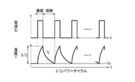
第1又は第2の実施の形態に係る半導体装置のΔTjパワーサイクルテストにおける電流ICと温度Tの変化の模式図は、図22に示すように表される。
第1又は第2の実施の形態に係る半導体装置のΔTjパワーサイクルテストにおける電流ICと温度Tの変化の模式図は、図22に示すように表される。
ΔTjパワーサイクルテストは、図22に示すように、接合温度を相対的に短時間の周期で上昇・下降させるテストであり、例えば、ワイヤ接合部などの寿命を評価することができる。
パワーサイクル試験の場合は、図22に示すように、半導体装置モジュールに通電・遮断を繰り返し、チップを発熱させる。第1又は第2の実施の形態に係る半導体装置のΔTjパワーサイクルテストにおいては、例えば、Tj=150℃を2s、その後オフして冷却温度になるまでの時間(例Tj=50℃、オフ時間=18s)を繰り返し行う。
[熱サイクルテスト]
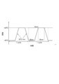
第1又は第2の実施の形態に係る半導体装置において、熱サイクルテストにおける温度プロファイル例は、図23に示すように表される。熱サイクルテストは大気雰囲気中で行われ、マイナス40℃~プラス150℃の範囲で実施した。熱サイクルの1サイクルの周期は80分であり、その内訳は、マイナス40℃で30分、マイナス40℃からプラス150℃までの昇温時間10分、プラス150℃で30分、プラス150℃からマイナス40℃までの冷却時間10分である。100サイクル毎に順方向電圧降下Vf、逆方向耐圧Vrを測定したが、特性劣化は観測されていない。
第1又は第2の実施の形態に係る半導体装置において、熱サイクルテストにおける温度プロファイル例は、図23に示すように表される。熱サイクルテストは大気雰囲気中で行われ、マイナス40℃~プラス150℃の範囲で実施した。熱サイクルの1サイクルの周期は80分であり、その内訳は、マイナス40℃で30分、マイナス40℃からプラス150℃までの昇温時間10分、プラス150℃で30分、プラス150℃からマイナス40℃までの冷却時間10分である。100サイクル毎に順方向電圧降下Vf、逆方向耐圧Vrを測定したが、特性劣化は観測されていない。
通常、熱サイクルテスト、もしくはパワーサイクル試験でも接合部の劣化が始まると、順方向などの高電流を流す試験では抵抗が増加し、順方向電圧Vfが変化する。
パワーサイクル耐量は特性劣化も含めて起こってもその劣化の進行が遅い場合には、パワーサイクル耐量が高いと評価することができる。
パワーサイクル耐量は特性劣化も含めて起こってもその劣化の進行が遅い場合には、パワーサイクル耐量が高いと評価することができる。
以上のΔTjパワーサイクルテストおよび熱サイクルテストの結果より、第1又は第2の実施の形態に係る半導体装置の銅ワイヤ18又は上部配線24の接合強度は、充分に確保されている。
なお、第1又は第2の実施の形態では、銀焼成キャップ22上に銅ワイヤ18又ははんだ26Aを配置することとしているが、これに限定されるものではない。例えば、銀焼成キャップ22上に銀焼成で上部配線24を接合するようにしてもよい。銀焼成キャップ22上に銀焼成することで膜厚を増加させることができる。これにより、はんだ26Aよりも高耐熱化を図ることができ、信頼性を向上させることが可能となる。
[半導体装置の具体例]
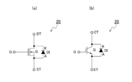
第1又は第2の実施の形態に係る半導体装置20であって、ワンインワンモジュールのSiC MISFETの模式的回路表現は、図24(a)に示すように表され、ワンインワンモジュールのIGBTの模式的回路表現は、図24(b)に示すように表される。
第1又は第2の実施の形態に係る半導体装置20であって、ワンインワンモジュールのSiC MISFETの模式的回路表現は、図24(a)に示すように表され、ワンインワンモジュールのIGBTの模式的回路表現は、図24(b)に示すように表される。
図24(a)には、MISFETQに逆並列接続されるダイオードDIが示されている。MISFETQの主電極は、ドレイン端子DTおよびソース端子STで表される。同様に、図24(b)には、IGBTQに逆並列接続されるダイオードDIが示されている。IGBTQの主電極は、コレクタ端子CTおよびエミッタ端子ETで表される。ダイオードDIとしては、ファーストリカバリダイオード(FRD)や、ショットキーバリアダイオード(SBD)を外付けしても良い。また、MISFETの半導体基板中に形成されるダイオードのみを用いても良い。
また、第1又は第2の実施の形態に係る半導体装置20であって、ワンインワンモジュールのSiC MISFETの詳細回路表現は、図25に示すように表される。
また、1つのモジュールに複数個のMISFETが内蔵されていても良い。一例として5チップ(MISFET×5)搭載可能であり、それぞれのMISFETQは、5個まで並列接続可能である。尚、5チップの内、一部をダイオードDI用として搭載することも可能である。
さらに詳細には、図25に示すように、MISFETQに並列にセンス用MISFETQsが接続される。センス用MISFETQsは、MISFETQと同一チップ内に、微細トランジスタとして形成されている。図25において、SSは、ソースセンス端子、CSは、電流センス端子であり、Gは、ゲート信号端子である。尚、第1又は第2の実施の形態においても半導体デバイスQには、センス用MISFETQsが同一チップ内に、微細トランジスタとして形成されている。
また、第1又は第2の実施の形態に係る半導体装置20Tであって、ツーインワンモジュールのSiC MISFETの模式的回路表現は、図26(a)に示すように表される。
図26(a)に示すように、2個のMISFETQ1・Q4と、MISFETQ1・Q4に逆並列接続されるダイオードD1・D4が1つのモジュールに内蔵されている。G1は、MISFETQ1のゲート信号端子であり、S1は、MISFETQ1のソース端子である。G4は、MISFETQ4のゲート信号端子であり、S4は、MISFETQ4のソース端子である。Pは、正側電源入力端子であり、Nは、負側電源入力端子であり、Oは、出力端子である。
また、第1又は第2の実施の形態に係る半導体装置20Tであって、ツーインワンモジュールのIGBTの模式的回路表現は、図26(b)に示すように表される。図26(b)に示すように、2個のIGBTQ1・Q4と、IGBTQ1・Q4に逆並列接続されるダイオードD1・D4が1つのモジュールに内蔵されている。G1は、IGBTQ1のゲート信号端子であり、E1は、IGBTQ1のエミッタ端子である。G4は、IGBTQ4のゲート信号端子であり、E4は、IGBTQ4のエミッタ端子である。Pは、正側電源入力端子であり、Nは、負側電源入力端子であり、Oは、出力端子である。
(半導体デバイスの構成例)
第1又は第2の実施の形態に適用可能な半導体デバイスの例であって、SiC MISFETの模式的断面構造は、図27(a)に示すように表され、IGBTの模式的断面構造は、図27(b)に示すように表される。
第1又は第2の実施の形態に適用可能な半導体デバイスの例であって、SiC MISFETの模式的断面構造は、図27(a)に示すように表され、IGBTの模式的断面構造は、図27(b)に示すように表される。
第1又は第2の実施の形態に適用可能な半導体デバイス110(Q)の例として、SiC MISFETの模式的断面構造は、図27(a)に示すように、n-高抵抗層からなる半導体基板126と、半導体基板126の表面側に形成されたpボディ領域128と、pボディ領域128の表面に形成されたソース領域130と、pボディ領域128間の半導体基板126の表面上に配置されたゲート絶縁膜132と、ゲート絶縁膜132上に配置されたゲート電極138と、ソース領域130およびpボディ領域128に接続されたソース電極134と、半導体基板126の表面と反対側の裏面に配置されたn+ドレイン領域124と、n+ドレイン領域124に接続されたドレイン電極136とを備える。
図27(a)では、半導体デバイス110は、プレーナゲート型nチャネル縦型SiC MISFETで構成されているが、後述する図31に示すように、nチャネル縦型SiC TMISFETなどで構成されていても良い。
また、第1又は第2の実施の形態に適用可能な半導体デバイス110(Q)には、SiC MISFETの代わりに、GaN系FETなどを採用することもできる。
第1又は第2の実施の形態に適用可能な半導体デバイス110には、SiC系、GaN系のいずれかのパワーデバイスを採用可能である。
さらには、第1又は第2の実施の形態に適用可能な半導体デバイス110には、バンドギャップエネルギーが、例えば、1.1eV~8eVのワイドギャップ型と云われる半導体を用いることができる。
同様に、第1又は第2の実施の形態に適用可能な半導体デバイス110A(Q)の例として、IGBTは、図27(b)に示すように、n-高抵抗層からなる半導体基板126と、半導体基板126の表面側に形成されたpボディ領域128と、pボディ領域128の表面に形成されたエミッタ領域130Eと、pボディ領域128間の半導体基板126の表面上に配置されたゲート絶縁膜132と、ゲート絶縁膜132上に配置されたゲート電極138と、エミッタ領域130Eおよびpボディ領域128に接続されたエミッタ電極134Eと、半導体基板126の表面と反対側の裏面に配置されたp+コレクタ領域124Pと、p+コレクタ領域124Pに接続されたコレクタ電極136Cとを備える。
図27(b)では、半導体デバイス110Aは、プレーナゲート型のnチャネル縦型IGBTで構成されているが、トレンチゲート型nチャネル縦型IGBTなどで構成されていても良い。
第1又は第2の実施の形態に適用可能な半導体デバイス110の例であって、ソースパッド電極SP、ゲートパッド電極GPを含むSiC MISFETの模式的断面構造は、図28に示すように表される。ゲートパッド電極GPは、ゲート絶縁膜132上に配置されたゲート電極138に接続され、ソースパッド電極SPは、ソース領域130およびpボディ領域128に接続されたソース電極134に接続される。
また、ゲートパッド電極GPおよびソースパッド電極SPは、図28に示すように、半導体デバイス110の表面を覆うパッシベーション用の層間絶縁膜144上に配置される。尚、ゲートパッド電極GPおよびソースパッド電極SPの下方の半導体基板126内には、図27(a)或いは、図28の中央部と同様に、微細構造のトランジスタ構造が形成されていても良い。
さらに、図28に示すように、中央部のトランジスタ構造においても、パッシベーション用の層間絶縁膜144上にソースパッド電極SPが延在して配置されていても良い。
第1又は第2の実施の形態に適用する半導体デバイス110Aの例であって、ソースパッド電極SP、ゲートパッド電極GPを含むIGBTの模式的断面構造は、図29に示すように表される。ゲートパッド電極GPは、ゲート絶縁膜132上に配置されたゲート電極138に接続され、エミッタパッド電極EPは、エミッタ領域130Eおよびpボディ領域128に接続されたエミッタ電極134Eに接続される。
また、ゲートパッド電極GPおよびエミッタパッド電極EPは、図29に示すように、半導体デバイス110Aの表面を覆うパッシベーション用の層間絶縁膜144上に配置される。尚、ゲートパッド電極GPおよびエミッタパッド電極EPの下方の半導体基板126内には、図27(b)或いは、図29の中央部と同様に、微細構造のIGBT構造が形成されていても良い。
さらに、図29に示すように、中央部のIGBT構造においても、パッシベーション用の層間絶縁膜144上にエミッタパッド電極EPが延在して配置されていても良い。
―SiC DIMISFET―
第1又は第2の実施の形態に適用可能な半導体デバイス110の例であって、SiC DIMISFETの模式的断面構造は、図30に示すように表される。
第1又は第2の実施の形態に適用可能な半導体デバイス110の例であって、SiC DIMISFETの模式的断面構造は、図30に示すように表される。
第1又は第2の実施の形態に適用可能なSiC DIMISFETは、図30に示すように、n-高抵抗層からなる半導体基板126と、半導体基板126の表面側に形成されたpボディ領域128と、pボディ領域128の表面に形成されたn+ソース領域130と、pボディ領域128間の半導体基板126の表面上に配置されたゲート絶縁膜132と、ゲート絶縁膜132上に配置されたゲート電極138と、ソース領域130およびpボディ領域128に接続されたソース電極134と、半導体基板126の表面と反対側の裏面に配置されたn+ドレイン領域124と、n+ドレイン領域124に接続されたドレイン電極136とを備える。
図30では、半導体デバイス110は、pボディ領域128と、pボディ領域128の表面に形成されたn+ソース領域130が、ダブルイオン注入(DI)で形成され、ソースパッド電極SPは、ソース領域130およびpボディ領域128に接続されたソース電極134に接続される。ゲートパッド電極GP(図示省略)は、ゲート絶縁膜132上に配置されたゲート電極138に接続される。また、ソースパッド電極SPおよびゲートパッド電極GP(図示省略)は、図30に示すように、半導体デバイス110の表面を覆うパッシベーション用の層間絶縁膜144上に配置される。
SiC DIMISFETは、図30に示すように、pボディ領域128に挟まれたn-高抵抗層からなる半導体基板126内に、破線で示されるような空乏層が形成されるため、接合型FET(JFET)効果に伴うチャネル抵抗RJFETが形成される。また、pボディ領域128/半導体基板126間には、図30に示すように、ボディダイオードBDが形成される。
―SiC TMISFET―
第1又は第2の実施の形態に適用可能な半導体デバイス110の例であって、SiC TMISFETの模式的断面構造は、図31に示すように表される。
第1又は第2の実施の形態に適用可能な半導体デバイス110の例であって、SiC TMISFETの模式的断面構造は、図31に示すように表される。
第1又は第2の実施の形態に適用可能なSiC TMISFETは、図31に示すように、n層からなる半導体基板126Nと、半導体基板126Nの表面側に形成されたpボディ領域128と、pボディ領域128の表面に形成されたn+ソース領域130と、pボディ領域128を貫通し、半導体基板126Nまで形成されたトレンチの内にゲート絶縁層132および層間絶縁膜144U・144Bを介して形成されたトレンチゲート電極138TGと、ソース領域130およびpボディ領域128に接続されたソース電極134と、半導体基板126Nの表面と反対側の裏面に配置されたn+ドレイン領域124と、n+ドレイン領域124に接続されたドレイン電極136とを備える。
図31では、半導体デバイス110は、pボディ領域128を貫通し、半導体基板126Nまで形成されたトレンチ内にゲート絶縁層132および層間絶縁膜144U・144Bを介して形成されたトレンチゲート電極138TGが形成され、ソースパッド電極SPは、ソース領域130およびpボディ領域128に接続されたソース電極134に接続される。ゲートパッド電極GP(図示省略)は、ゲート絶縁膜132上に配置されたゲート電極138に接続される。また、ソースパッド電極SPおよびゲートパッド電極GP(図示省略)は、図31に示すように、半導体デバイス110の表面を覆うパッシベーション用の層間絶縁膜144U上に配置される。
SiC TMISFETでは、SiC DIMISFETのような接合型FET(JFET)効果に伴うチャネル抵抗RJFETは形成されない。また、pボディ領域128/半導体基板126N間には、ボディダイオードBDが形成される。
第1又は第2の実施の形態に係る半導体装置を用いて構成した3相交流インバータ140の模式的回路構成において、半導体デバイスとしてSiC MISFETを適用し、電源端子PL、接地端子NL間にスナバコンデンサCを接続した回路構成例は、図32(a)に示すように表される。同様に、第1又は第2の実施の形態に係る半導体装置を用いて構成した3相交流インバータ140Aの模式的回路構成において、半導体デバイスとしてIGBTを適用し、電源端子PL、接地端子NL間にスナバコンデンサCを接続した回路構成例は、図32(b)に示すように表される。
第1又は第2の実施の形態に係る半導体装置を電源Eと接続する際、接続ラインの有するインダクタンスLによって、SiC MISFETやIGBTのスイッチング速度が速いため、大きなサージ電圧Ldi/dtを生ずる。例えば、電流変化di=300A、スイッチングに伴う時間変化dt=100nsecとすると、di/dt=3×109(A/s)となる。インダクタンスLの値により、サージ電圧Ldi/dtの値は変化するが、電源Vにこのサージ電圧Ldi/dtが重畳される。電源端子PLと接地端子NL間に接続されるスナバコンデンサCによって、このサージ電圧Ldi/dtを吸収することができる。
(半導体装置を適用した応用例)
次に、図33を参照して、半導体デバイスとしてSiC MISFETを適用した第1又は第2の実施の形態に係る半導体装置を用いて構成した3相交流インバータ140について説明する。
次に、図33を参照して、半導体デバイスとしてSiC MISFETを適用した第1又は第2の実施の形態に係る半導体装置を用いて構成した3相交流インバータ140について説明する。
図33に示すように、3相交流インバータ140は、ゲートドライブ部150と、ゲートドライブ部150に接続された半導体装置部152と、3相交流モータ部154とを備える。半導体装置部152は、3相交流モータ部154のU相、V相、W相に対応して、U相、V相、W相のインバータが接続されている。ここで、ゲートドライブ部150は、SiC MISFETQ1・Q4、SiC MISFETQ2・Q5、およびSiC MISFETQ3・Q6に接続されている。
半導体装置部152は、蓄電池(E)146が接続されたコンバータ148のプラス端子(+)とマイナス端子(-)間に接続され、インバータ構成のSiC MISFETQ1・Q4、Q2・Q5、およびQ3・Q6を備える。また、SiC MISFETQ1~Q6のソース・ドレイン間には、フリーホイールダイオードD1~D6がそれぞれ逆並列に接続されている。
次に、図34を参照して、半導体デバイスとしてIGBTを適用した第1又は第2の実施の形態に係る半導体装置20Tを用いて構成した3相交流インバータ140Aについて説明する。
図34に示すように、3相交流インバータ140Aは、ゲートドライブ部150Aと、ゲートドライブ部150Aに接続された半導体装置部152Aと、3相交流モータ部154Aとを備える。半導体装置部152Aは、3相交流モータ部154AのU相、V相、W相に対応して、U相、V相、W相のインバータが接続されている。ここで、ゲートドライブ部150Aは、IGBTQ1・Q4、IGBTQ2・Q5、およびIGBTQ3・Q6に接続されている。
半導体装置部152Aは、蓄電池(E)146Aが接続されたコンバータ148Aのプラス端子(+)とマイナス端子(-)間に接続され、インバータ構成のIGBTQ1・Q4、Q2・Q5、およびQ3・Q6を備える。さらに、IGBTQ1~Q6のエミッタ・コレクタ間には、フリーホイールダイオードD1~D6がそれぞれ逆並列に接続されている。
本実施の形態に係る半導体装置或いはパワーモジュールは、ワンインワン、ツーインワン、フォーインワン、シックスインワン若しくはセブンインワン型のいずれにも形成可能である。
以上説明したように、本実施の形態によれば、パワーサイクル耐量を向上させることが可能な半導体装置、パワーモジュール及びその製造方法を提供することができる。
[その他の実施の形態]
上記のように、実施の形態について記載したが、この開示の一部をなす論述および図面は例示的なものであり、限定するものであると理解すべきではない。この開示から当業者には様々な代替実施の形態、実施例および運用技術が明らかとなろう。
上記のように、実施の形態について記載したが、この開示の一部をなす論述および図面は例示的なものであり、限定するものであると理解すべきではない。この開示から当業者には様々な代替実施の形態、実施例および運用技術が明らかとなろう。
このように、ここでは記載していない様々な実施の形態などを含む。
本実施の形態の半導体装置およびパワーモジュールは、IGBTモジュール、ダイオードモジュール、MOSモジュール(Si、SiC、GaN)等の半導体モジュール作製技術に利用することができ、HEV/EV向けのインバータ、産業機器向けのインバータ、コンバータなど幅広い応用分野に適用可能である。
10B…第1の基板電極
12…半導体チップ
14…ソースパッド電極
16…ゲートパッド電極
17A,17B,26A,26B…はんだ
18…銅ワイヤ
20B…第2の基板電極
22…高耐熱性の焼成膜(銀焼成キャップ,銅焼成キャップ)
24…上部配線
25…酸化膜
26…アルミニウム電極
28…金薄膜
Tj…ジャンクション温度
12…半導体チップ
14…ソースパッド電極
16…ゲートパッド電極
17A,17B,26A,26B…はんだ
18…銅ワイヤ
20B…第2の基板電極
22…高耐熱性の焼成膜(銀焼成キャップ,銅焼成キャップ)
24…上部配線
25…酸化膜
26…アルミニウム電極
28…金薄膜
Tj…ジャンクション温度
Claims (24)
- 表面側および裏面側に電極が形成された半導体チップと、
前記半導体チップの表面側の少なくとも一部の電極を覆うように形成される高耐熱性の焼成膜と
を備えることを特徴とする半導体装置。 - 前記半導体チップが第1の基板電極上に配置され、
前記高耐熱性の焼成膜上にワイヤの一方端が接合されていることを特徴とする請求項1に記載の半導体装置。 - 前記ワイヤは、銅ワイヤ、Alワイヤ若しくはクラッドワイヤを備え、
前記ワイヤの一方端が超音波接合されていることを特徴とする請求項2に記載の半導体装置。 - 前記半導体チップが第1の基板電極上に配置され、
はんだを接合材として前記高耐熱性の焼成膜上に平板状の上部配線の一方端が接合されることを特徴とする請求項1に記載の半導体装置。 - 前記高耐熱性の焼成膜は、銀焼成膜であることを特徴とする請求項1に記載の半導体装置。
- 前記高耐熱性の焼成膜は、銅焼成膜であることを特徴とする請求項1に記載の半導体装置。
- 前記電極と前記焼成膜との間に、金薄膜、銀薄膜、若しくはパラジウム膜のいずれかの電極表面薄膜を備えることを特徴とする請求項1~6のいずれか1項に記載の半導体装置。
- 前記焼成膜の厚さは、10μm~100μmの範囲であることを特徴とする請求項1~7のいずれか1項に記載の半導体装置。
- 前記半導体チップは、MISFETを備え、
前記半導体チップ上の電極は、ソースパッド電極を備えることを特徴とする請求項1に記載の半導体装置。 - 請求項1~9のいずれか1項に記載の半導体装置を複数個備えることを特徴とするパワーモジュール。
- 前記半導体チップは、ワイドギャップ型半導体を備えることを特徴とする請求項1に記載の半導体装置。
- 前記半導体チップは、100℃以上のΔTjパワーサイクルを備えることを特徴とする請求項1に記載の半導体装置。
- 絶縁性の基板と、
前記基板上に形成された第1乃至第3の基板電極と、
前記第1の基板電極上に配置され、その表面側および裏面側に電極が形成された半導体チップと、
前記半導体チップの表面側の少なくとも一部の電極を覆うように形成される高耐熱性の焼成膜と、
前記焼成膜と前記第2の基板電極との間を接続する第1の上部配線と、
前記半導体チップの表面側の前記焼成膜に覆われていない電極と前記第3の基板電極との間を接続する第2の上部配線と、
前記第1乃至第3の基板電極と前記半導体チップと前記第1および第2の上部配線を封止する樹脂と
を備えることを特徴とする半導体装置。 - 前記焼成膜と前記第1の上部配線との間に前記焼成膜よりも厚いはんだ層を有することを特徴とする請求項13に記載の半導体装置。
- 前記第1の上部配線の厚みは、前記半導体チップと前記焼成膜との厚みよりも厚いことを特徴とする請求項13または14に記載の半導体装置。
- 前記焼成膜が複数形成されており、複数の前記焼成膜を同一の前記第1の上部配線で共通接続することを特徴とする請求項13~15のいずれか1項に記載の半導体装置。
- 半導体チップ上の電極を覆うように高耐熱性の導電性膜を形成する工程と、
前記高耐熱性の導電性膜を焼成する工程と
を有することを特徴とする半導体装置の製造方法。 - 前記半導体チップが第1の基板電極上に配置され、
超音波により前記高耐熱性の導電性膜上に銅ワイヤ若しくはAlワイヤの一方端が接合されることを特徴とする請求項17に記載の半導体装置の製造方法。 - 前記半導体チップが第1の基板電極上に配置され、
はんだを接合材として前記高耐熱性の焼成膜上に平板状の上部配線の一方端が接合されることを特徴とする請求項17に記載の半導体装置の製造方法。 - 前記高耐熱性の焼成膜は、銀焼成膜若しくは銅焼成膜を備えることを特徴とする請求項17に記載の半導体装置の製造方法。
- 前記高耐熱性の焼成膜は、マスク印刷若しくはディスペンス法により形成されることを特徴とする請求項17に記載の半導体装置の製造方法。
- 前記電極上にメッキ工程で金薄膜、銀薄膜、若しくはパラジウム薄膜のいずれかの薄膜が形成され、前記薄膜上に前記高耐熱性の焼成膜が形成されることを特徴とする請求項17に記載の半導体装置の製造方法。
- 前記半導体チップは、MISFETを備え、
前記半導体チップ上の電極は、ソースパッド電極を備えることを特徴とする請求項17に記載の半導体装置の製造方法。 - 前記半導体チップは、複数チップを備えることを特徴とする請求項17~23のいずれか1項に記載の半導体装置の製造方法。
Priority Applications (8)
| Application Number | Priority Date | Filing Date | Title |
|---|---|---|---|
| CN201780024218.2A CN109075086B (zh) | 2016-04-19 | 2017-04-14 | 半导体装置、功率模块及其制造方法 |
| CN202210844102.6A CN115020258A (zh) | 2016-04-19 | 2017-04-14 | 半导体装置、功率模块、半导体装置的制造方法及半导体模块 |
| DE112017002080.8T DE112017002080T5 (de) | 2016-04-19 | 2017-04-14 | Halbleiterbauteil, leistungsmodul und herstellungsverfahren für das halbleiterbauteil |
| JP2018513160A JP6935392B2 (ja) | 2016-04-19 | 2017-04-14 | 半導体装置、パワーモジュール及びその製造方法 |
| US16/136,988 US10790247B2 (en) | 2016-04-19 | 2018-09-20 | Semiconductor device and fabrication method of the semiconductor device |
| US16/925,017 US11189586B2 (en) | 2016-04-19 | 2020-07-09 | Semiconductor device and fabrication method of the semiconductor device |
| US17/512,366 US11658140B2 (en) | 2016-04-19 | 2021-10-27 | Semiconductor device and fabrication method of the semiconductor device |
| US18/300,157 US12074129B2 (en) | 2016-04-19 | 2023-04-13 | Semiconductor device and fabrication method of the semiconductor device |
Applications Claiming Priority (2)
| Application Number | Priority Date | Filing Date | Title |
|---|---|---|---|
| JP2016083634 | 2016-04-19 | ||
| JP2016-083634 | 2016-04-19 |
Related Child Applications (1)
| Application Number | Title | Priority Date | Filing Date |
|---|---|---|---|
| US16/136,988 Continuation US10790247B2 (en) | 2016-04-19 | 2018-09-20 | Semiconductor device and fabrication method of the semiconductor device |
Publications (1)
| Publication Number | Publication Date |
|---|---|
| WO2017183580A1 true WO2017183580A1 (ja) | 2017-10-26 |
Family
ID=60116016
Family Applications (1)
| Application Number | Title | Priority Date | Filing Date |
|---|---|---|---|
| PCT/JP2017/015306 Ceased WO2017183580A1 (ja) | 2016-04-19 | 2017-04-14 | 半導体装置、パワーモジュール及びその製造方法 |
Country Status (5)
| Country | Link |
|---|---|
| US (4) | US10790247B2 (ja) |
| JP (4) | JP6935392B2 (ja) |
| CN (2) | CN109075086B (ja) |
| DE (1) | DE112017002080T5 (ja) |
| WO (1) | WO2017183580A1 (ja) |
Cited By (2)
| Publication number | Priority date | Publication date | Assignee | Title |
|---|---|---|---|---|
| JP2022047892A (ja) * | 2020-09-14 | 2022-03-25 | 三菱電機株式会社 | 半導体装置およびその製造方法 |
| JP2023139229A (ja) * | 2018-10-09 | 2023-10-03 | ローム株式会社 | 半導体装置 |
Families Citing this family (5)
| Publication number | Priority date | Publication date | Assignee | Title |
|---|---|---|---|---|
| CN121126834A (zh) * | 2015-12-18 | 2025-12-12 | 罗姆股份有限公司 | 半导体装置 |
| JP6935392B2 (ja) * | 2016-04-19 | 2021-09-15 | ローム株式会社 | 半導体装置、パワーモジュール及びその製造方法 |
| JP7371393B2 (ja) * | 2019-08-22 | 2023-10-31 | 富士電機株式会社 | 駆動装置、半導体装置及びゲート駆動方法 |
| CN112201628A (zh) * | 2020-08-24 | 2021-01-08 | 株洲中车时代半导体有限公司 | 一种功率模块封装结构及其制备方法 |
| WO2024232130A1 (ja) * | 2023-05-09 | 2024-11-14 | 株式会社新川 | 半導体装置の製造方法 |
Citations (3)
| Publication number | Priority date | Publication date | Assignee | Title |
|---|---|---|---|---|
| JP2009179825A (ja) * | 2008-01-29 | 2009-08-13 | Daiken Chemical Co Ltd | 電子部品の電極接続方法及び電子部品 |
| JP2014082367A (ja) * | 2012-10-17 | 2014-05-08 | Nippon Micrometal Corp | パワー半導体装置 |
| JP2016004796A (ja) * | 2014-06-13 | 2016-01-12 | ローム株式会社 | パワーモジュールおよびその製造方法 |
Family Cites Families (17)
| Publication number | Priority date | Publication date | Assignee | Title |
|---|---|---|---|---|
| JP2000100849A (ja) * | 1998-09-24 | 2000-04-07 | Sony Corp | 半導体装置およびその製造方法 |
| DE102006034679A1 (de) * | 2006-07-24 | 2008-01-31 | Infineon Technologies Ag | Halbleitermodul mit Leistungshalbleiterchip und passiven Bauelement sowie Verfahren zur Herstellung desselben |
| JP4708399B2 (ja) | 2007-06-21 | 2011-06-22 | 新光電気工業株式会社 | 電子装置の製造方法及び電子装置 |
| JP5882069B2 (ja) * | 2011-03-29 | 2016-03-09 | エスアイアイ・セミコンダクタ株式会社 | 半導体装置及びその製造方法 |
| JP5822656B2 (ja) * | 2011-10-31 | 2015-11-24 | 株式会社 日立パワーデバイス | 半導体装置及びその製造方法 |
| WO2013125022A1 (ja) * | 2012-02-24 | 2013-08-29 | 株式会社日立製作所 | 半導体装置 |
| JP6084367B2 (ja) * | 2012-04-06 | 2017-02-22 | 株式会社 日立パワーデバイス | 半導体装置 |
| JP5804203B2 (ja) * | 2012-07-11 | 2015-11-04 | 三菱電機株式会社 | 半導体装置およびその製造方法 |
| JP6161251B2 (ja) * | 2012-10-17 | 2017-07-12 | ルネサスエレクトロニクス株式会社 | 半導体装置およびその製造方法 |
| CN103811446B (zh) | 2012-11-15 | 2016-08-10 | 万国半导体(开曼)股份有限公司 | 一种半导体器件中的铜线键接结构及其制造方法 |
| JP5975911B2 (ja) * | 2013-03-15 | 2016-08-23 | ルネサスエレクトロニクス株式会社 | 半導体装置 |
| US9054091B2 (en) * | 2013-06-10 | 2015-06-09 | Alpha & Omega Semiconductor, Inc. | Hybrid packaged lead frame based multi-chip semiconductor device with multiple semiconductor chips and multiple interconnecting structures |
| DE102014104272A1 (de) * | 2014-03-26 | 2015-10-01 | Heraeus Deutschland GmbH & Co. KG | Träger und Clip jeweils für ein Halbleiterelement, Verfahren zur Herstellung, Verwendung und Sinterpaste |
| JP6272213B2 (ja) * | 2014-11-26 | 2018-01-31 | 三菱電機株式会社 | 半導体装置 |
| WO2016084241A1 (ja) * | 2014-11-28 | 2016-06-02 | 日産自動車株式会社 | ハーフブリッジパワー半導体モジュール及びその製造方法 |
| TW201721832A (zh) * | 2015-12-10 | 2017-06-16 | 力智電子股份有限公司 | 具熱感測功能的功率金氧半電晶體晶粒以及積體電路 |
| JP6935392B2 (ja) * | 2016-04-19 | 2021-09-15 | ローム株式会社 | 半導体装置、パワーモジュール及びその製造方法 |
-
2017
- 2017-04-14 JP JP2018513160A patent/JP6935392B2/ja active Active
- 2017-04-14 DE DE112017002080.8T patent/DE112017002080T5/de active Pending
- 2017-04-14 CN CN201780024218.2A patent/CN109075086B/zh active Active
- 2017-04-14 CN CN202210844102.6A patent/CN115020258A/zh active Pending
- 2017-04-14 WO PCT/JP2017/015306 patent/WO2017183580A1/ja not_active Ceased
-
2018
- 2018-09-20 US US16/136,988 patent/US10790247B2/en active Active
-
2020
- 2020-07-09 US US16/925,017 patent/US11189586B2/en active Active
-
2021
- 2021-08-24 JP JP2021136430A patent/JP7175359B2/ja active Active
- 2021-10-27 US US17/512,366 patent/US11658140B2/en active Active
-
2022
- 2022-11-07 JP JP2022178415A patent/JP7494271B2/ja active Active
-
2023
- 2023-04-13 US US18/300,157 patent/US12074129B2/en active Active
-
2024
- 2024-05-21 JP JP2024082690A patent/JP7747819B2/ja active Active
Patent Citations (3)
| Publication number | Priority date | Publication date | Assignee | Title |
|---|---|---|---|---|
| JP2009179825A (ja) * | 2008-01-29 | 2009-08-13 | Daiken Chemical Co Ltd | 電子部品の電極接続方法及び電子部品 |
| JP2014082367A (ja) * | 2012-10-17 | 2014-05-08 | Nippon Micrometal Corp | パワー半導体装置 |
| JP2016004796A (ja) * | 2014-06-13 | 2016-01-12 | ローム株式会社 | パワーモジュールおよびその製造方法 |
Cited By (5)
| Publication number | Priority date | Publication date | Assignee | Title |
|---|---|---|---|---|
| JP2023139229A (ja) * | 2018-10-09 | 2023-10-03 | ローム株式会社 | 半導体装置 |
| JP7623437B2 (ja) | 2018-10-09 | 2025-01-28 | ローム株式会社 | 半導体装置 |
| US12315821B2 (en) | 2018-10-09 | 2025-05-27 | Rohm Co., Ltd. | Semiconductor device and method for manufacturing semiconductor device |
| JP2022047892A (ja) * | 2020-09-14 | 2022-03-25 | 三菱電機株式会社 | 半導体装置およびその製造方法 |
| JP7412310B2 (ja) | 2020-09-14 | 2024-01-12 | 三菱電機株式会社 | 半導体装置およびその製造方法 |
Also Published As
| Publication number | Publication date |
|---|---|
| US10790247B2 (en) | 2020-09-29 |
| JP7494271B2 (ja) | 2024-06-03 |
| JP7175359B2 (ja) | 2022-11-18 |
| JP2023015214A (ja) | 2023-01-31 |
| JPWO2017183580A1 (ja) | 2019-02-21 |
| US20190019771A1 (en) | 2019-01-17 |
| CN109075086B (zh) | 2022-07-15 |
| US11658140B2 (en) | 2023-05-23 |
| CN109075086A (zh) | 2018-12-21 |
| JP2024105667A (ja) | 2024-08-06 |
| JP2021185615A (ja) | 2021-12-09 |
| DE112017002080T5 (de) | 2019-01-24 |
| US20230253352A1 (en) | 2023-08-10 |
| US20220052003A1 (en) | 2022-02-17 |
| US11189586B2 (en) | 2021-11-30 |
| CN115020258A (zh) | 2022-09-06 |
| JP6935392B2 (ja) | 2021-09-15 |
| JP7747819B2 (ja) | 2025-10-01 |
| US12074129B2 (en) | 2024-08-27 |
| US20200343208A1 (en) | 2020-10-29 |
Similar Documents
| Publication | Publication Date | Title |
|---|---|---|
| JP7535606B2 (ja) | パワー半導体装置およびその製造方法 | |
| JP7494271B2 (ja) | 半導体装置及びパワーモジュール | |
| US10483216B2 (en) | Power module and fabrication method for the same | |
| US9673163B2 (en) | Semiconductor device with flip chip structure and fabrication method of the semiconductor device | |
| JP6097013B2 (ja) | パワーモジュール半導体装置 | |
| JP6077773B2 (ja) | パワーモジュール半導体装置 | |
| CN103928408B (zh) | 功率半导体模块和用于制造功率半导体模块的方法 | |
| JP6192561B2 (ja) | 電力用半導体装置 | |
| JP6591808B2 (ja) | パワーモジュールおよびインバータ装置 | |
| CN110476244B (zh) | 功率模块及其制造方法 | |
| JP5899952B2 (ja) | 半導体モジュール | |
| US20230028808A1 (en) | Semiconductor device | |
| JP6630762B2 (ja) | パワーモジュール |
Legal Events
| Date | Code | Title | Description |
|---|---|---|---|
| WWE | Wipo information: entry into national phase |
Ref document number: 2018513160 Country of ref document: JP |
|
| 121 | Ep: the epo has been informed by wipo that ep was designated in this application |
Ref document number: 17785918 Country of ref document: EP Kind code of ref document: A1 |
|
| 122 | Ep: pct application non-entry in european phase |
Ref document number: 17785918 Country of ref document: EP Kind code of ref document: A1 |