WO2017170535A1 - 回路モジュール - Google Patents
回路モジュール Download PDFInfo
- Publication number
- WO2017170535A1 WO2017170535A1 PCT/JP2017/012613 JP2017012613W WO2017170535A1 WO 2017170535 A1 WO2017170535 A1 WO 2017170535A1 JP 2017012613 W JP2017012613 W JP 2017012613W WO 2017170535 A1 WO2017170535 A1 WO 2017170535A1
- Authority
- WO
- WIPO (PCT)
- Prior art keywords
- electrode
- multilayer substrate
- inner layer
- circuit module
- extraction electrode
- Prior art date
- Legal status (The legal status is an assumption and is not a legal conclusion. Google has not performed a legal analysis and makes no representation as to the accuracy of the status listed.)
- Ceased
Links
Images




Classifications
-
- H—ELECTRICITY
- H10—SEMICONDUCTOR DEVICES; ELECTRIC SOLID-STATE DEVICES NOT OTHERWISE PROVIDED FOR
- H10W—GENERIC PACKAGES, INTERCONNECTIONS, CONNECTORS OR OTHER CONSTRUCTIONAL DETAILS OF DEVICES COVERED BY CLASS H10
- H10W70/00—Package substrates; Interposers; Redistribution layers [RDL]
- H10W70/60—Insulating or insulated package substrates; Interposers; Redistribution layers
- H10W70/67—Insulating or insulated package substrates; Interposers; Redistribution layers characterised by their insulating layers or insulating parts
- H10W70/68—Shapes or dispositions thereof
- H10W70/685—Shapes or dispositions thereof comprising multiple insulating layers
-
- H—ELECTRICITY
- H05—ELECTRIC TECHNIQUES NOT OTHERWISE PROVIDED FOR
- H05K—PRINTED CIRCUITS; CASINGS OR CONSTRUCTIONAL DETAILS OF ELECTRIC APPARATUS; MANUFACTURE OF ASSEMBLAGES OF ELECTRICAL COMPONENTS
- H05K1/00—Printed circuits
- H05K1/02—Details
-
- H—ELECTRICITY
- H05—ELECTRIC TECHNIQUES NOT OTHERWISE PROVIDED FOR
- H05K—PRINTED CIRCUITS; CASINGS OR CONSTRUCTIONAL DETAILS OF ELECTRIC APPARATUS; MANUFACTURE OF ASSEMBLAGES OF ELECTRICAL COMPONENTS
- H05K1/00—Printed circuits
- H05K1/02—Details
- H05K1/0213—Electrical arrangements not otherwise provided for
- H05K1/0216—Reduction of cross-talk, noise or electromagnetic interference
- H05K1/0218—Reduction of cross-talk, noise or electromagnetic interference by printed shielding conductors, ground planes or power plane
-
- H—ELECTRICITY
- H05—ELECTRIC TECHNIQUES NOT OTHERWISE PROVIDED FOR
- H05K—PRINTED CIRCUITS; CASINGS OR CONSTRUCTIONAL DETAILS OF ELECTRIC APPARATUS; MANUFACTURE OF ASSEMBLAGES OF ELECTRICAL COMPONENTS
- H05K3/00—Apparatus or processes for manufacturing printed circuits
- H05K3/46—Manufacturing multilayer circuits
-
- H—ELECTRICITY
- H05—ELECTRIC TECHNIQUES NOT OTHERWISE PROVIDED FOR
- H05K—PRINTED CIRCUITS; CASINGS OR CONSTRUCTIONAL DETAILS OF ELECTRIC APPARATUS; MANUFACTURE OF ASSEMBLAGES OF ELECTRICAL COMPONENTS
- H05K9/00—Screening of apparatus or components against electric or magnetic fields
-
- H—ELECTRICITY
- H05—ELECTRIC TECHNIQUES NOT OTHERWISE PROVIDED FOR
- H05K—PRINTED CIRCUITS; CASINGS OR CONSTRUCTIONAL DETAILS OF ELECTRIC APPARATUS; MANUFACTURE OF ASSEMBLAGES OF ELECTRICAL COMPONENTS
- H05K9/00—Screening of apparatus or components against electric or magnetic fields
- H05K9/0007—Casings
- H05K9/002—Casings with localised screening
- H05K9/0022—Casings with localised screening of components mounted on printed circuit boards [PCB]
- H05K9/0024—Shield cases mounted on a PCB, e.g. cans or caps or conformal shields
-
- H—ELECTRICITY
- H05—ELECTRIC TECHNIQUES NOT OTHERWISE PROVIDED FOR
- H05K—PRINTED CIRCUITS; CASINGS OR CONSTRUCTIONAL DETAILS OF ELECTRIC APPARATUS; MANUFACTURE OF ASSEMBLAGES OF ELECTRICAL COMPONENTS
- H05K9/00—Screening of apparatus or components against electric or magnetic fields
- H05K9/0007—Casings
- H05K9/002—Casings with localised screening
- H05K9/0039—Galvanic coupling of ground layer on printed circuit board [PCB] to conductive casing
-
- H—ELECTRICITY
- H10—SEMICONDUCTOR DEVICES; ELECTRIC SOLID-STATE DEVICES NOT OTHERWISE PROVIDED FOR
- H10W—GENERIC PACKAGES, INTERCONNECTIONS, CONNECTORS OR OTHER CONSTRUCTIONAL DETAILS OF DEVICES COVERED BY CLASS H10
- H10W42/00—Arrangements for protection of devices
- H10W42/20—Arrangements for protection of devices protecting against electromagnetic or particle radiation, e.g. light, X-rays, gamma-rays or electrons
-
- H—ELECTRICITY
- H10—SEMICONDUCTOR DEVICES; ELECTRIC SOLID-STATE DEVICES NOT OTHERWISE PROVIDED FOR
- H10W—GENERIC PACKAGES, INTERCONNECTIONS, CONNECTORS OR OTHER CONSTRUCTIONAL DETAILS OF DEVICES COVERED BY CLASS H10
- H10W42/00—Arrangements for protection of devices
- H10W42/20—Arrangements for protection of devices protecting against electromagnetic or particle radiation, e.g. light, X-rays, gamma-rays or electrons
- H10W42/261—Arrangements for protection of devices protecting against electromagnetic or particle radiation, e.g. light, X-rays, gamma-rays or electrons characterised by their shapes or dispositions
- H10W42/276—Arrangements for protection of devices protecting against electromagnetic or particle radiation, e.g. light, X-rays, gamma-rays or electrons characterised by their shapes or dispositions the arrangements being on an external surface of the package, e.g. on the outer surface of an encapsulation
-
- H—ELECTRICITY
- H10—SEMICONDUCTOR DEVICES; ELECTRIC SOLID-STATE DEVICES NOT OTHERWISE PROVIDED FOR
- H10W—GENERIC PACKAGES, INTERCONNECTIONS, CONNECTORS OR OTHER CONSTRUCTIONAL DETAILS OF DEVICES COVERED BY CLASS H10
- H10W70/00—Package substrates; Interposers; Redistribution layers [RDL]
- H10W70/60—Insulating or insulated package substrates; Interposers; Redistribution layers
- H10W70/62—Insulating or insulated package substrates; Interposers; Redistribution layers characterised by their interconnections
- H10W70/63—Vias, e.g. via plugs
- H10W70/635—Through-vias
-
- H—ELECTRICITY
- H10—SEMICONDUCTOR DEVICES; ELECTRIC SOLID-STATE DEVICES NOT OTHERWISE PROVIDED FOR
- H10W—GENERIC PACKAGES, INTERCONNECTIONS, CONNECTORS OR OTHER CONSTRUCTIONAL DETAILS OF DEVICES COVERED BY CLASS H10
- H10W70/00—Package substrates; Interposers; Redistribution layers [RDL]
- H10W70/60—Insulating or insulated package substrates; Interposers; Redistribution layers
- H10W70/62—Insulating or insulated package substrates; Interposers; Redistribution layers characterised by their interconnections
- H10W70/65—Shapes or dispositions of interconnections
-
- H—ELECTRICITY
- H10—SEMICONDUCTOR DEVICES; ELECTRIC SOLID-STATE DEVICES NOT OTHERWISE PROVIDED FOR
- H10W—GENERIC PACKAGES, INTERCONNECTIONS, CONNECTORS OR OTHER CONSTRUCTIONAL DETAILS OF DEVICES COVERED BY CLASS H10
- H10W72/00—Interconnections or connectors in packages
- H10W72/20—Bump connectors, e.g. solder bumps or copper pillars; Dummy bumps; Thermal bumps
-
- H—ELECTRICITY
- H10—SEMICONDUCTOR DEVICES; ELECTRIC SOLID-STATE DEVICES NOT OTHERWISE PROVIDED FOR
- H10W—GENERIC PACKAGES, INTERCONNECTIONS, CONNECTORS OR OTHER CONSTRUCTIONAL DETAILS OF DEVICES COVERED BY CLASS H10
- H10W74/00—Encapsulations, e.g. protective coatings
-
- H—ELECTRICITY
- H10—SEMICONDUCTOR DEVICES; ELECTRIC SOLID-STATE DEVICES NOT OTHERWISE PROVIDED FOR
- H10W—GENERIC PACKAGES, INTERCONNECTIONS, CONNECTORS OR OTHER CONSTRUCTIONAL DETAILS OF DEVICES COVERED BY CLASS H10
- H10W74/00—Encapsulations, e.g. protective coatings
- H10W74/10—Encapsulations, e.g. protective coatings characterised by their shape or disposition
- H10W74/111—Encapsulations, e.g. protective coatings characterised by their shape or disposition the semiconductor body being completely enclosed
- H10W74/114—Encapsulations, e.g. protective coatings characterised by their shape or disposition the semiconductor body being completely enclosed by a substrate and the encapsulations
-
- H—ELECTRICITY
- H10—SEMICONDUCTOR DEVICES; ELECTRIC SOLID-STATE DEVICES NOT OTHERWISE PROVIDED FOR
- H10W—GENERIC PACKAGES, INTERCONNECTIONS, CONNECTORS OR OTHER CONSTRUCTIONAL DETAILS OF DEVICES COVERED BY CLASS H10
- H10W74/00—Encapsulations, e.g. protective coatings
- H10W74/40—Encapsulations, e.g. protective coatings characterised by their materials
- H10W74/47—Encapsulations, e.g. protective coatings characterised by their materials comprising organic materials, e.g. plastics or resins
-
- H—ELECTRICITY
- H10—SEMICONDUCTOR DEVICES; ELECTRIC SOLID-STATE DEVICES NOT OTHERWISE PROVIDED FOR
- H10W—GENERIC PACKAGES, INTERCONNECTIONS, CONNECTORS OR OTHER CONSTRUCTIONAL DETAILS OF DEVICES COVERED BY CLASS H10
- H10W99/00—Subject matter not provided for in other groups of this subclass
-
- H—ELECTRICITY
- H10—SEMICONDUCTOR DEVICES; ELECTRIC SOLID-STATE DEVICES NOT OTHERWISE PROVIDED FOR
- H10W—GENERIC PACKAGES, INTERCONNECTIONS, CONNECTORS OR OTHER CONSTRUCTIONAL DETAILS OF DEVICES COVERED BY CLASS H10
- H10W90/00—Package configurations
- H10W90/701—Package configurations characterised by the relative positions of pads or connectors relative to package parts
- H10W90/721—Package configurations characterised by the relative positions of pads or connectors relative to package parts of bump connectors
- H10W90/724—Package configurations characterised by the relative positions of pads or connectors relative to package parts of bump connectors between a chip and a stacked insulating package substrate, interposer or RDL
-
- H—ELECTRICITY
- H10—SEMICONDUCTOR DEVICES; ELECTRIC SOLID-STATE DEVICES NOT OTHERWISE PROVIDED FOR
- H10W—GENERIC PACKAGES, INTERCONNECTIONS, CONNECTORS OR OTHER CONSTRUCTIONAL DETAILS OF DEVICES COVERED BY CLASS H10
- H10W90/00—Package configurations
- H10W90/701—Package configurations characterised by the relative positions of pads or connectors relative to package parts
- H10W90/751—Package configurations characterised by the relative positions of pads or connectors relative to package parts of bond wires
- H10W90/754—Package configurations characterised by the relative positions of pads or connectors relative to package parts of bond wires between a chip and a stacked insulating package substrate, interposer or RDL
Definitions
- the present invention relates to a circuit module.
- a configuration is known in which a plurality of components are mounted on the surface of a multilayer substrate, the components are covered with a resin, and a shield layer is formed on the surface of the resin (see, for example, Patent Document 1).
- the shield layer is connected to the ground electrode inside the multilayer substrate on the surface or side surface of the multilayer substrate.
- the multilayer substrate is formed by laminating and press-bonding a plurality of insulator layers, and pattern wirings are respectively formed on the insulator layers.
- the density of the pattern wiring is different for each insulator layer, and the shrinkage behavior between the insulator layer and the pattern wiring at the time of firing the substrate is different, so that the multilayer substrate may be warped or wavy.
- connection reliability means the mechanical and electrical connection reliability of any two electrodes, etc., and will be described below as electrical connection reliability. That is, increasing the connection reliability between the shield electrode and the inner layer ground electrode means lowering the resistance between the shield electrode and the inner layer ground electrode.
- an object of the present invention is to provide a circuit module capable of improving the connection reliability between the shield electrode and the inner layer ground electrode.
- a circuit module includes an inner layer ground electrode, a multilayer substrate having an extraction electrode drawn from the inner layer ground electrode, a mounting component mounted on the multilayer substrate, A resin that covers the mounting component, and a shield electrode that covers at least a part of a side surface of the resin and the multilayer substrate, the extraction electrode is electrically connected to the inner layer ground electrode in the multilayer substrate, And at least part of the multilayer substrate is disposed so as to overlap the inner layer ground electrode when viewed in the stacking direction of the multilayer substrate, and an end portion is exposed from a side surface of the multilayer substrate and connected to the shield electrode, The electrode has an end portion exposed from the side surface of the multilayer substrate and connected to the shield electrode.
- the connection reliability between the shield electrode and the inner layer ground electrode can be improved.
- the multilayer substrate has one or more pattern wirings that constitute a predetermined circuit together with the mounting component in an inner layer, and the end portions of the extraction electrodes have other density of the pattern wirings when viewed in the stacking direction. It may be connected to the shield electrode on the side of the multilayer substrate close to the lower part.
- warping and undulation are particularly likely to occur on the side of the multilayer substrate close to a portion where the density of the pattern wiring is lower than the others. Therefore, when the end of the extraction electrode is connected to the shield electrode in such a side, the extraction electrode is disposed in the vicinity of the side, and the side edge of the multilayer substrate that is likely to be warped and swelled. Generation
- production of these in a part can be suppressed.
- by arranging the extraction electrode it is possible to reduce and uniformize the unevenness of the pattern electrode density in the multilayer substrate, and thus it is possible to suppress warping and undulation of the multilayer substrate. That is, the occurrence of warpage and undulation of the multilayer substrate can be effectively suppressed.
- the extraction electrode may be arranged directly on the inner layer ground electrode.
- the parasitic inductance between the inner layer ground electrode and the extraction electrode can be reduced as compared with the case where the inner layer ground electrode and the extraction electrode are connected via a via or the like. Therefore, since the extraction electrode can be an electrically strong ground, the shield function by the shield electrode can be further enhanced.
- a plurality of the extraction electrodes may be arranged on the same layer of the multilayer substrate.
- the extraction electrode may include an upper extraction electrode disposed on the upper side of the inner layer ground electrode and a lower extraction electrode disposed on the lower side of the inner layer ground electrode.
- the electrodes upper extraction electrode and lower extraction electrode
- these occurrences are further reduced at the side end of the multilayer substrate where warpage and undulation are likely to occur. Can be suppressed. For this reason, the connection reliability between the shield electrode and the inner layer ground electrode can be further enhanced.
- an extraction electrode upper extraction electrode or lower extraction electrode
- the shield electrode and the inner layer ground can be used regardless of the warp and undulation of the multilayer substrate. Connection reliability with the electrode can be increased.
- the upper extraction electrode and the lower extraction electrode may be alternately arranged along the side of the multilayer substrate when viewed in the stacking direction.
- the thickness of the extraction electrode in the stacking direction can be made uniform. Therefore, warpage and undulation of the multilayer substrate can be further suppressed.
- the multilayer substrate may further include a dummy electrode disposed at a position that does not overlap the extraction electrode when viewed in the stacking direction.
- the multilayer substrate may further include a BAS paste layer disposed at a position that does not overlap with the extraction electrode when viewed in the stacking direction.
- the thickness of the multilayer substrate can be made uniform to further suppress warping and undulation.
- the inner layer ground electrode may be disposed on substantially the entire multilayer substrate when viewed in the stacking direction.
- the layout flexibility of the extraction electrode arranged so that at least a part thereof overlaps with the inner layer ground electrode can be increased.
- the extraction electrode may be disposed only at an end portion of the multilayer substrate when viewed in the stacking direction.
- a circuit module capable of enhancing the connection reliability between the inner layer ground electrode and the shield electrode is provided.
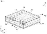
- FIG. 1 is a perspective view of a circuit module according to Embodiment 1.
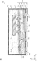
- FIG. FIG. 2 is a cross-sectional view of the circuit module according to the first embodiment.
- FIG. 3 is a layout diagram showing the arrangement of extraction electrodes in the circuit module according to the first embodiment.
- FIG. 4 is a cross-sectional view of a circuit module according to Modification 1 of Embodiment 1.
- FIG. 5 is a layout diagram showing the arrangement of the extraction electrodes in the circuit module according to the second modification of the first embodiment.
- FIG. 6 is a cross-sectional view of a circuit module according to the third modification of the first embodiment.
- FIG. 7 is a cross-sectional view of the circuit module according to the second embodiment.
- FIG. 8 is a layout diagram showing the arrangement of the upper extraction electrode and the lower extraction electrode in the circuit module according to the second embodiment.
- FIG. 1 is a perspective view of a circuit module 1 according to the first embodiment.
- the thickness direction of the circuit module 1 (that is, the stacking direction of the multilayer substrate 10) is described as a Z-axis direction, and directions perpendicular to the Z-axis direction and perpendicular to each other are defined as an X-axis direction and a Y-axis direction.
- the direction plus side will be described as the top surface (upper surface) side of the circuit module 1.
- the thickness direction of the circuit module 1 may not be the vertical direction.
- the top surface side of the circuit module 1 is not limited to the top surface side.
- viewing in the stacking direction of the multilayer substrate 10 viewing in parallel with the Z axis
- viewing in the stacking direction is simply referred to as viewing in the stacking direction.
- the circuit module 1 is a module component that constitutes a predetermined circuit such as a front-end circuit. As shown in FIG. 1, the circuit module 1 includes a multilayer substrate 10, mounting components 21 to 23 mounted on the multilayer substrate 10, a resin 30 covering the mounting components 21 to 23, and the side surfaces of the resin 30 and the multilayer substrate 10. And a shield electrode 40 that covers at least a part thereof.
- FIG. 2 is a cross-sectional view of the circuit module 1 according to the first embodiment. Specifically, this figure is a cross-sectional view taken along the line II-II in FIG.
- the multilayer substrate 10 includes a multilayer body 11 composed of base layers 111 to 118 and various conductors arranged on the base layers 111 to 118.
- the pattern wiring 121 which is a conductor formed along the main surfaces of the base material layers 111 to 118 (along the XY plane) and the base material layers 111 to 118 are arranged in the thickness direction (Z-axis direction).
- vias 122 that are conductors formed therethrough.
- an inner layer ground electrode 131 and a lead electrode 132 drawn from the inner layer ground electrode 131 are further arranged in the inner layer of the multilayer substrate 10 (that is, the inner layer of the multilayer body 11). Details of the inner layer ground electrode 131 and the extraction electrode 132 will be described later.
- being arranged in the inner layer of the multilayer substrate 10 means that the vertical direction is sandwiched between the base material layers so that it is not exposed on the upper surface or the lower surface of the multilayer substrate 10.
- a surface electrode 141 for mounting the mounting components 21 to 23 is disposed on the upper surface of the multilayer substrate 10, and a surface electrode for mounting the circuit module 1 on, for example, a motherboard is disposed on the lower surface of the multilayer substrate 10. 142 is arranged.
- a dummy electrode 151 is further arranged on the inner layer of the multilayer substrate 10.
- the dummy electrode 151 is an independent electrode that is not connected to other electrodes or the like, or an electrode that is connected only to the inner layer ground electrode 131. That is, the dummy electrode 151 is an electrode that does not change the circuit configuration of a predetermined circuit configured by the circuit module 1.
- the dummy electrode 151 is disposed directly on the inner layer ground electrode 131. Details of the dummy electrode 151 will be described later together with details of the inner ground electrode 131 and the extraction electrode 132.
- the material of the multilayer substrate 10 is not particularly limited.
- a ceramic such as LTCC (Low Temperature Co-fired Ceramic) or a resin such as polyimide can be used.
- a resin such as polyimide
- the conductor for example, silver or copper can be used.
- the method for forming the multilayer substrate 10 is not particularly limited.
- a silver or copper conductive paste for forming the conductor is screen-printed on a ceramic green sheet. And can be formed by co-firing.
- the mounting components 21 to 23 are components that constitute a predetermined circuit together with various conductors arranged on the multilayer substrate, and are, for example, a switch IC (Integrated Circuit), a filter, a duplexer, an oscillator, a chip capacitor, or a chip inductor.
- the mounting components 21 to 23 are not limited to LGA (Land Grid Array) type or BGA (Ball Grid Array) type components, but may be wire bonding mounting components.
- the resin 30 is a sealing member that covers and seals the mounting components 21 to 23.
- the resin 30 is disposed on the entire top surface of the multilayer substrate 10 so as to cover the mounting components 21 to 23.
- the resin 30 may not cover a part of the upper surface of the multilayer substrate 10.
- the material of the resin 30 is not particularly limited, but, for example, an epoxy resin can be used.
- the method for forming the resin 30 is not particularly limited. For example, when the resin 30 is formed using a liquid resin, the liquid resin is applied with a dispenser or the like so as to cover the mounting components 21 to 23 on the upper surface of the multilayer substrate 10. Then, the resin 30 can be formed by heating and curing. Further, when the resin 30 is formed using a solid resin, the resin 30 can be formed by placing a predetermined amount of the solid resin on the upper surface of the multilayer substrate 10, then heating and melting, and then curing. .
- the shield electrode 40 covers at least a part of the resin 30 and the side surface of the multilayer substrate 10, and is arranged so as to cover substantially the entire outer surface of the resin 30 and the side surface of the multilayer substrate 10 in the present embodiment. Specifically, the shield electrode 40 is disposed so as to cover the upper surface and side surfaces of the resin 30 and the side surfaces of the base material layers 111 to 117 of the multilayer substrate 10. The shield electrode 40 is connected to at least the extraction electrode 132 on the side surface of the multilayer substrate 10. For this reason, it has the shielding function which suppresses radiation
- the material of the shield electrode 40 is not particularly limited, but for example, silver or the like can be used.
- the method for forming the shield electrode 40 is not particularly limited, but for example, it can be formed as follows. Specifically, the multilayer substrate 10 and the assembly of the resin 30 on which the mounting components 21 to 23 are mounted are half-cut (the base material layers 111 to 117 are cut while leaving the base material layer 118). The inner layer ground electrode 131 and the extraction electrode 132 are exposed on the side surfaces of the first electrode.
- a conductive paste such as silver is applied to the side surface of the multilayer substrate 10 and the resin 30, or is electrically connected to the inner layer ground electrode 131 and the extraction electrode 132 on the side surface of the multilayer substrate 10 by a method such as sputtering or vapor deposition.
- the shield electrode 40 to be connected can be formed.
- the assembly of the multilayer substrate 10 and the resin 30 on which the mounting components 21 to 23 are mounted may be completely cut (all of the base material layers 111 to 118 are cut). That is, the shield electrode 40 may be disposed so as to cover the side surfaces of the base material layers 111 to 118 of the multilayer substrate 10.
- the inner layer ground electrode 131 is a ground electrode arranged in the inner layer of the multilayer substrate 10, and in the present embodiment, it is a so-called solid pattern electrode arranged in substantially the entire multilayer substrate 10 when viewed in the stacking direction. . Note that “substantially whole” not only means completely the whole but also means substantially the whole. That is, the inner layer ground electrode 131 may have a portion that is not locally disposed so as to avoid the via 122 different from the ground potential in the in-plane direction orthogonal to the stacking direction.
- the inner layer ground electrode 131 has an end portion exposed from the side surface of the multilayer substrate 10 and connected to the shield electrode 40. That is, the inner layer ground electrode 131 and the shield electrode 40 are electrically connected to each other. Specifically, the inner layer ground electrode 131 is exposed from the side surface of the multilayer substrate 10 in the circumferential direction as viewed in the stacking direction (ie, all four sides).
- the inner-layer ground electrode 131 does not have to be exposed at all the end portions in the circumferential direction when viewed in the stacking direction.
- the end portions are exposed at two opposite sides of the multilayer substrate 10 when viewed in the stacking direction.
- the end portions may be exposed at two adjacent sides. That is, the inner layer ground electrode 131 is not limited to the solid pattern electrode, and may be an electrode disposed between two different side surfaces of the multilayer substrate 10.
- the extraction electrode 132 is a ground electrode extracted from the inner layer ground electrode 131 and is disposed in the inner layer of the multilayer substrate 10.
- the extraction electrode 132 is electrically connected to the inner layer ground electrode 131 in the multilayer substrate 10, and is arranged so that at least a part thereof overlaps the inner layer ground electrode 131 when viewed in the stacking direction of the multilayer substrate 10. .
- the inner layer ground electrode 131 is a solid pattern electrode, the extraction electrode 132 is disposed so as to overlap the inner layer ground electrode 131 as viewed in the stacking direction.
- the end of the extraction electrode 132 is exposed from the side surface of the multilayer substrate 10 and connected to the shield electrode 40. That is, the extraction electrode 132 is an electrode that is extracted from the inner layer ground electrode 131 to the side surface of the multilayer substrate 10.
- the extraction electrode 132 is directly disposed on the inner layer ground electrode 131. That is, the extraction electrode 132 is conductively connected to the inner layer ground electrode 131 without the via 122. Specifically, the extraction electrode 132 is disposed on the upper side (Z-axis direction plus side) of the inner layer ground electrode 131 and is directly disposed on the inner layer ground electrode 131 (in this case, the upper surface of the inner layer ground electrode 131). ing.
- a plurality of extraction electrodes 132 are arranged on the same layer of the multilayer substrate 10. Specifically, as shown in FIG. 2, a plurality of extraction electrodes 132 are arranged between the base material layer 117 and the base material layer 118 of the multilayer substrate 10.
- FIG. 3 is a layout diagram showing the arrangement of the extraction electrodes 132 in the circuit module 1 according to the first embodiment.
- the arrangement of the dummy electrodes 151 is also shown.
- the extraction electrode 132 and the dummy electrode 151 are hatched for simplicity. The same applies to the following layout diagrams.
- the area A shown in the figure shows a portion where the density of the pattern wiring 121 is relatively high. That is, as viewed in the stacking direction, the region excluding the region A in the multilayer substrate 10 is a portion where the density of the pattern wiring 121 is lower than that of the region A.
- the region A is a region that can be determined from the distribution state of the pattern wiring 121 on the multilayer substrate 10, for example, and is a region where the ratio of the thickness of the pattern wiring 121 to the thickness of the multilayer substrate 10 is a predetermined value (for example, average) or more.
- the region A may be a region that can be appropriately determined depending on, for example, the design matters of the multilayer substrate 10, and the pattern wiring 121 that is restricted by circuit characteristics and strength required for the multilayer substrate 10 can be disposed. It may be a region.
- the extraction electrode 132 is disposed only at the end of the multilayer substrate 10 when viewed in the stacking direction. Further, the end portion of the extraction electrode 132 is connected to the shield electrode 40 on the side of the multilayer substrate 10 that is close to the portion where the density of the pattern wiring 121 is lower than the others (that is, the region excluding the region A) when viewed in the stacking direction. Has been. Specifically, as shown in FIG. 3, since the region A is located at the center of the multilayer substrate 10, the density of the pattern wiring 121 is low at the peripheral edge of the multilayer substrate 10. For this reason, the end portion of the extraction electrode 132 is connected to the shield electrode 40 at sides (here, four sides) close to the peripheral portion.
- the extraction electrode 132 only needs to be connected to the shield electrode 40 on the side of the multilayer substrate 10 close to the portion where the density of the pattern wiring 121 is low, and at least a part thereof is a portion where the density of the pattern wiring 121 is high (that is, It may be arranged in the area A) of FIG. Further, the side close to the portion where the density of the pattern wiring 121 is low means the side closest to the portion where the density is low, and particularly means the side along the portion where the density is low.
- a plurality of extraction electrodes 132 are arranged, for example, at regular intervals along the side of the multilayer substrate 10 when viewed in the stacking direction.
- positions the extraction electrode 132 is not specifically limited, From the viewpoint of suppressing the curvature and waviness of the multilayer substrate 10, what is necessary is just to determine suitably.
- the arrangement interval of the extraction electrodes 132 is not limited to an equal interval, and for example, the interval may be narrower as the density of the pattern wiring 121 is lower.
- the dummy electrode 151 is disposed at a position where it does not overlap with the extraction electrode 132 when viewed in the stacking direction.
- the arrangement position of the dummy electrode 151 is not particularly limited as long as it does not overlap with the extraction electrode 132 as described above, but from the viewpoint of suppressing warpage and undulation of the multilayer substrate 10, the pattern wiring 121 is viewed in the stacking direction. It is preferable to arrange in a portion having a low density.
- the dummy electrode 151 is preferably disposed in a portion of the region A where the density of the pattern wiring 121 is relatively low.
- connection reliability between the shield electrode 40 and the inner-layer ground electrode 131 is improved as compared with the circuit module according to the comparative example that does not include the extraction electrode 132. Can be increased.
- the heat shrinkage rate between the resin or ceramic forming the base layer and the silver or copper forming the conductor such as the pattern wiring is different, and thus the step of heating the multilayer substrate
- warping and undulation may occur in the multilayer substrate.
- a shield electrode connected to the inner layer ground electrode is arranged on the side surface of the multilayer substrate with respect to the multilayer substrate in which such warpage or undulation has occurred, a connection failure between the shield electrode and the inner layer ground electrode is likely to occur, and these connections There is a problem that reliability decreases.
- the end portions of the inner layer ground electrode 131 and the extraction electrode 132 are exposed from the side surfaces of the multilayer substrate 10 and connected to the shield electrode 40.
- connection reliability between the shield electrode 40 and the inner layer ground electrode 131 can be improved.
- the end portion of the extraction electrode 132 is shielded by the side of the multilayer substrate 10 that is close to the portion where the density of the pattern wiring 121 is lower than the other when viewed in the stacking direction. It is connected to the electrode 40.
- the extraction electrode 132 when the end portion of the extraction electrode 132 is connected to the shield electrode 40 in such a side, the extraction electrode 132 is disposed in the vicinity of the side, and the multilayer substrate 10 is likely to be warped and swelled. Generation
- the extraction electrode 132 by arranging the extraction electrode 132, the unevenness of the pattern electrode density in the multilayer substrate 10 can be reduced and uniformized, so that warpage and undulation of the multilayer substrate 10 can be suppressed. That is, the occurrence of warpage and undulation of the multilayer substrate 10 can be effectively suppressed.
- the extraction electrode 132 is directly disposed on the inner layer ground electrode 131.
- the parasitic inductance between the inner layer ground electrode 131 and the extraction electrode 132 can be reduced as compared with the case where the inner layer ground electrode 131 and the extraction electrode 132 are connected via the via 122 or the like. Therefore, since the extraction electrode 132 can be an electrically strong ground, the shield function by the shield electrode 40 can be further enhanced.
- the circuit module 1 since the plurality of extraction electrodes 132 are arranged on the same layer of the multilayer substrate 10, the total contact area between the shield electrode 40 and the extraction electrode 132 can be reduced. It can be secured greatly. Therefore, the connection reliability between the shield electrode 40 and the inner layer ground electrode 131 can be further enhanced.
- the circuit module 1 by having the dummy electrode 151, the variation in the conductor distribution in the multilayer substrate 10 can be further reduced and uniformized. Therefore, warpage and undulation of the multilayer substrate 10 can be further suppressed.
- the inner layer ground electrode 131 is disposed on substantially the entire multilayer substrate 10 when viewed in the stacking direction, so that at least a part thereof overlaps with the inner layer ground electrode 131.
- the degree of freedom in layout of the extraction electrode 132 disposed in the substrate can be increased.
- the extraction electrode 132 is arranged only at the end of the multilayer substrate 10 when viewed in the stacking direction, an increase in the thickness of the entire multilayer substrate 10 is suppressed. Meanwhile, warping and undulation of the multilayer substrate 10 can be suppressed.
- the extraction electrode may not be directly disposed on the inner layer ground electrode 131, and may be connected to the inner layer ground electrode 131 via the via 122, for example.
- FIG. 4 is a cross-sectional view of a circuit module 1A according to the first modification of the first embodiment.
- the circuit module 1A shown in the figure is different from the circuit module 1 shown in FIG. 2 in that the extraction electrode 132A is connected to the inner layer ground electrode 131 through the via 122.
- the end portions of the inner-layer ground electrode 131 and the extraction electrode 132A are exposed from the side surfaces of the multilayer substrate 10 and connected to the shield electrode 40, as in the first embodiment. By doing so, the connection reliability between the shield electrode 40 and the inner layer ground electrode 131 can be improved.
- the extraction electrodes 132 are arranged at equal intervals along the side of the multilayer substrate 10 when viewed in the stacking direction.
- the present invention is not limited to this.
- FIG. 5 is a layout diagram showing the arrangement of the extraction electrodes 132B in the circuit module 1B according to the second modification of the first embodiment.
- the extraction electrode 132B shown in the figure is extended along the side of the multilayer substrate 10 when viewed in the stacking direction as compared with the extraction electrode 132 shown in FIG.
- the end portions of the inner ground electrode 131 and the extraction electrode 132B are exposed from the side surfaces of the multilayer substrate 10 and connected to the shield electrode 40, as in the first embodiment. By doing so, the connection reliability between the shield electrode 40 and the inner layer ground electrode 131 can be improved.
- the extraction electrode 132B is arranged independently for each side of the multilayer substrate 10 when viewed in the stacking direction.
- the present invention is not limited to this, for example, two adjacent sides of the multilayer substrate 10 It may be arranged continuously, or may be annularly extended along the side of the multilayer substrate 10.
- a BAS paste layer may be further disposed on the inner layer of the multilayer substrate 10.
- FIG. 6 is a cross-sectional view of a circuit module 1C according to the third modification of the first embodiment.
- the circuit module 1 ⁇ / b> C shown in FIG. 2 further has a BAS paste layer 161 arranged at a position where the multilayer substrate 10 does not overlap with the extraction electrode 132 when viewed in the stacking direction. The point is different.
- the BAS paste layer 161 is an insulator layer that is disposed in a layer different from the inner layer ground electrode 131 and is disposed in substantially the same shape and position as the dummy electrode 151 when viewed in the stacking direction.
- the BAS paste layer 161 may be disposed at a position that does not overlap with the extraction electrode 132 when viewed in the stacking direction, and the shape and the arrangement position are not particularly limited.
- the pattern wiring 121 is disposed in a portion where the density is low as viewed in the stacking direction.
- the BAS paste layer 161 is preferably disposed in a portion of the region A (see FIG. 3) where the density of the pattern wiring 121 is relatively low.
- the material of the BAS paste layer 161 is not particularly limited.
- a dielectric material mainly composed of Ba (barium), Al (aluminum), and Si (silicon) can be used.
- the end portions of the inner ground electrode 131 and the extraction electrode 132 are exposed from the side surfaces of the multilayer substrate 10 and connected to the shield electrode 40, as in the first embodiment. By doing so, the connection reliability between the shield electrode 40 and the inner layer ground electrode 131 can be improved.
- the multilayer substrate 10 has the BAS paste layer 161, whereby the thickness of the entire multilayer substrate 10 can be made uniform.
- the thickness of the entire multilayer substrate 10 depends on the distribution of conductors in the multilayer substrate 10, and becomes thicker at a portion where the conductor density is high, and thinner at a lower portion. In such a portion where the thickness of the multilayer substrate 10 is thin, waviness is particularly likely to occur. For this reason, by disposing the BAS paste layer 161 in a portion where the density of the conductor is low, the thickness of the multilayer substrate 10 can be made uniform and warpage and undulation can be further suppressed.
- the extraction electrode is disposed only in one layer in the multilayer substrate 10. However, the extraction electrode may be arranged in a plurality of layers in the multilayer substrate 10. In the first embodiment and the modification thereof, the dummy electrode 151 is disposed in the multilayer substrate 10, but the dummy electrode 151 may not be disposed. Thus, hereinafter, a circuit module having such a configuration will be described as a second embodiment.
- FIG. 7 is a cross-sectional view of the circuit module 2 according to the second embodiment.
- the circuit module 2 shown in the figure has an upper extraction electrode 232 and a lower extraction electrode 233 instead of the extraction electrode 132A, and no dummy electrode 151 is arranged. Is different. Since the upper extraction electrode 232 corresponds to the above-described extraction electrode 132A, the following description will mainly focus on the items related to the lower extraction electrode 233, and the upper extraction electrode 232 will be simplified as appropriate.
- circuit module 2 is different from the circuit module 1A in the layer in which the inner layer ground electrode 131 and the upper lead electrode 232 are arranged, but these layers may be the same layer as the circuit module 1A.
- the lower extraction electrode 233 is an extraction electrode arranged below the inner layer ground electrode 131.
- the lower extraction electrode 233 is connected to the inner ground electrode 131 via the via 122.
- the lower extraction electrode 233 may be directly disposed on the inner layer ground electrode 131 (in this case, the lower surface of the inner layer ground electrode 131, that is, the negative side in the Z-axis direction) without using the via 122.
- the upper extraction electrode 232 and the lower extraction electrode 233 are arranged as shown in FIG. 8 in the present embodiment.
- FIG. 8 is a layout diagram showing the arrangement of the upper extraction electrode 232 and the lower extraction electrode 233 in the circuit module 2 according to the second embodiment.
- the upper extraction electrode 232 and the lower extraction electrode 233 are arranged at positions that do not overlap each other when viewed in the stacking direction, specifically, alternately arranged along the side of the multilayer substrate 10.
- the upper extraction electrode 232 and the lower extraction electrode 233 are arranged in substantially the same shape and size.
- the upper extraction electrode 232 and the lower extraction electrode 233 may be arranged in different shapes or sizes.
- the upper extraction electrode 232 and the lower extraction electrode 233 may be made of the same material, or may be made of different materials.
- each of the inner-layer ground electrode 131 and the extraction electrode in this modification, the upper extraction electrode 232 and the lower extraction electrode 233), as in the first embodiment. Since the end portion is exposed from the side surface of the multilayer substrate 10 and connected to the shield electrode 40, the connection reliability between the shield electrode 40 and the inner layer ground electrode 131 can be improved.
- the upper extraction electrode 232 and the lower extraction electrode 233 are arranged as extraction electrodes.
- these occurrences are further reduced at the side end portions of the multilayer substrate 10 where warpage and undulation are likely to occur. Can be suppressed. For this reason, the connection reliability between the shield electrode 40 and the inner layer ground electrode 131 can be further enhanced.
- the shield can be used regardless of the warp and undulation of the multilayer substrate 10.
- the connection reliability between the electrode 40 and the inner layer ground electrode 131 can be improved.
- the multilayer substrate 10 is warped in a convex shape upward or in a convex shape depending on the distribution state of the pattern wiring 121 in the multilayer substrate 10 and the arrangement positions of the mounting components 21 to 23.
- the extraction electrode that can ensure the contact area with the shield electrode 40 can be replaced with the upper extraction electrode 232 and the lower extraction electrode 233. Therefore, by arranging the upper extraction electrode 232 and the lower extraction electrode 233, the connection reliability between the shield electrode 40 and the inner ground electrode 131 can be improved regardless of the warp and undulation of the multilayer substrate 10. .
- the upper extraction electrode 232 and the lower extraction electrode 233 are alternately arranged when viewed in the stacking direction, thereby uniformizing the thickness of the extraction electrode in the stacking direction. can do. Therefore, warpage and undulation of the multilayer substrate 10 can be further suppressed.
- circuit module according to the embodiment of the present invention and the modification thereof has been described above, the present invention is not limited to the individual embodiment and the modification thereof. Unless it deviates from the gist of the present invention, various modifications conceived by those skilled in the art have been made in this embodiment and its modifications, and forms constructed by combining different embodiments and components in those modifications, It may be included within the scope of one or more embodiments of the invention.
- the end portion of the extraction electrode is connected to the shield electrode 40 on the side of the multilayer substrate 10 that is close to the portion where the density of the pattern wiring 121 is lower than the other when viewed in the stacking direction.
- the end portion of the extraction electrode may be connected to the shield electrode 40 on the side of the multilayer substrate 10 close to the portion where the density of the pattern wiring 121 is high.
- a plurality of extraction electrodes are arranged on the same layer of the multilayer substrate 10.
- only one extraction electrode may be arranged on the same layer of the multilayer substrate 10.
- the upper extraction electrode 232 and the lower extraction electrode 233 are alternately arranged as viewed in the stacking direction.
- each of the upper extraction electrode 232 and the lower extraction electrode 233 is provided. However, they may be arranged consecutively.
- each of the dummy electrode 151 and the BAS paste layer 161 may be disposed at a position at least partially overlapping with the extraction electrode when viewed in the stacking direction.
- the multilayer substrate 10 may include a plurality of sets each including one inner layer ground electrode 131 and an extraction electrode extracted from the one inner layer ground electrode.
- the extraction electrode is preferably connected to the inner layer ground electrode 131 without passing through the pattern wiring 121 (that is, drawn from the inner layer ground electrode 131), but the inner layer ground is connected through the pattern wiring 121. It may be connected to the electrode 131.
- the extraction electrode may be arranged only at a part of the peripheral edge of the multilayer substrate 10 when viewed in the stacking direction. That is, the shield electrode 40 may be connected to the extraction electrode only on one side surface among all the side surfaces of the multilayer substrate 10.
- the present invention can be widely used in communication devices such as mobile phones as circuit module parts.
Landscapes
- Engineering & Computer Science (AREA)
- Microelectronics & Electronic Packaging (AREA)
- Physics & Mathematics (AREA)
- Manufacturing & Machinery (AREA)
- Electromagnetism (AREA)
- Structure Of Printed Boards (AREA)
- Production Of Multi-Layered Print Wiring Board (AREA)
- Shielding Devices Or Components To Electric Or Magnetic Fields (AREA)
- Non-Metallic Protective Coatings For Printed Circuits (AREA)
- Structures Or Materials For Encapsulating Or Coating Semiconductor Devices Or Solid State Devices (AREA)
- Condensed Matter Physics & Semiconductors (AREA)
- General Physics & Mathematics (AREA)
- Geometry (AREA)
- Health & Medical Sciences (AREA)
- Toxicology (AREA)
Abstract
本発明に係る回路モジュール(1)は、内層グランド電極(131)及び当該内層グランド電極(131)から引き出された引出電極(132)を内層に有する多層基板(10)と、多層基板(10)に実装された実装部品(21~23)と、実装部品(21~23)を覆う樹脂(30)と、樹脂(30)及び多層基板(10)の側面の少なくとも一部を覆うシールド電極(40)とを備え、引出電極(132)は、多層基板(10)内で内層グランド電極(131)と電気的に接続され、かつ、多層基板(10)の積層方向に見て少なくとも一部が内層グランド電極(131)に重なるように配置され、端部が多層基板(10)の側面から露出してシールド電極(40)に接続されており、内層グランド電極(131)は、端部が多層基板(10)の側面から露出してシールド電極(40)に接続されている。
Description
本発明は、回路モジュールに関する。
回路モジュールとして、多層基板表面に複数の部品を実装し、その部品を樹脂で被覆し、樹脂の表面にシールド層を形成する構成が知られている(例えば、特許文献1参照)。この構成によれば、シールド層は、多層基板の表面または側面において多層基板内部のグランド電極と接続される。
しかしながら、多層基板は複数の絶縁体層を積層及び圧着することにより形成されており、その絶縁体層上にはそれぞれパターン配線が形成されている。パターン配線の密度は絶縁体層ごとに相違しており、基板焼成時の絶縁体層とパターン配線との収縮挙動が異なるため、多層基板に反りやうねりが発生する場合がある。
このような反りやうねりが発生すると、多層基板の内層グランド電極とシールド電極とが多層基板の側面で接続される構成では、内層グランド電極に対するシールド電極の接触面積が低下して、シールド電極と内層グランド電極との接続信頼性が低下する場合がある。このとき、シールド電極のシールド機能が低下し、所望のモジュール特性が得られないという問題がある。
なお、接続信頼性とは任意の2つの電極等の機械的及び電気的な接続信頼性を意味し、以下では、特に電気的な接続信頼性として説明する。つまり、シールド電極と内層グランド電極との接続信頼性を高めるとは、シールド電極と内層グランド電極との間の抵抗を低抵抗化することを意味する。
そこで、本発明は、シールド電極と内層グランド電極との接続信頼性を高めることができる回路モジュールを提供することを目的とする。
上記目的を達成するために、本発明の一態様に係る回路モジュールは、内層グランド電極及び当該内層グランド電極から引き出された引出電極を有する多層基板と、前記多層基板に実装された実装部品と、前記実装部品を覆う樹脂と、前記樹脂、及び前記多層基板の側面の少なくとも一部を覆うシールド電極とを備え、前記引出電極は、前記多層基板内で前記内層グランド電極と電気的に接続され、かつ、前記多層基板の積層方向に見て少なくとも一部が前記内層グランド電極に重なるように配置され、端部が前記多層基板の側面から露出して前記シールド電極に接続されており、前記内層グランド電極は、端部が前記多層基板の側面から露出して前記シールド電極に接続されている。
このように、内層グランド電極及び引出電極それぞれの端部が多層基板の側面から露出してシールド電極に接続されていることにより、シールド電極と内層グランド電極との接続信頼性を高めることができる。
また、前記多層基板は、前記実装部品とともに所定の回路を構成する1以上のパターン配線を内層に有し、前記引出電極の端部は、前記積層方向に見て、前記パターン配線の密度が他よりも低い部分に近接する前記多層基板の辺において、前記シールド電極に接続されていることにしてもよい。
ここで、パターン配線の密度が他よりも低い部分に近接する多層基板の辺では、特に反り及びうねりが発生しやすい。そこで、このような辺において引出電極の端部がシールド電極に接続されることにより、当該辺の近傍に引出電極が配置されることになり、反り及びうねりが発生しやすい多層基板の側方端部におけるこれらの発生を抑制することができる。具体的には、引出電極を配置することにより、多層基板におけるパターン電極密度の偏りを低減して均一化させることができるため、多層基板の反り及びうねりを抑制することができる。つまり、多層基板の反り及びうねりが発生しやすい部分において、これらの発生を効果的に抑制することができる。
また、前記引出電極は、前記内層グランド電極上に直接配置されていることにしてもよい。
これにより、内層グランド電極と引出電極とがビア等を介して接続される場合に比べて、内層グランド電極と引出電極との間の寄生インダクタンスを低減することができる。よって、引出電極を電気的に強固なグランドとすることができるため、シールド電極によるシールド機能を一層高めることができる。
また、前記多層基板の同一の層に、複数の前記引出電極が配置されていることにしてもよい。
このように、多層基板の同一の層に複数の引出電極が配置されていることにより、シールド電極と引出電極との接触面積を大きく確保することができる。よって、シールド電極と内層グランド電極との接続信頼性を一層高めることができる。
また、前記引出電極は、前記内層グランド電極よりも上側に配置された上側引出電極と、前記内層グランド電極よりも下側に配置された下側引出電極とを含むことにしてもよい。
このように引出電極として複数層に配置された電極(上側引出電極及び下側引出電極)を配置することにより、反り及びうねりが発生しやすい多層基板の側方端部において、これらの発生を一層抑制することができる。このため、シールド電極と内層グランド電極との接続信頼性を一層高めることができる。また、内層グランド電極の上側及び下側のそれぞれに引出電極(上側引出電極または下側引出電極)が配置されていることにより、多層基板の反り及びうねりの態様によらず、シールド電極と内層グランド電極との接続信頼性を高めることができる。
また、前記上側引出電極と前記下側引出電極とは、前記積層方向に見て、前記多層基板の辺に沿って交互に配置されることにしてもよい。
これにより、積層方向における引出電極の厚みを均一化することができる。よって、多層基板の反り及びうねりを一層抑制することができる。
また、前記多層基板は、さらに、前記積層方向に見て前記引出電極と重ならない位置に配置されたダミー電極を有することにしてもよい。
このようなダミー電極を有することにより、多層基板における導体の分布のバラつきを一層低減して均一化させることができる。よって、多層基板の反り及びうねりを一層抑制することができる。
また、前記多層基板は、さらに、前記積層方向に見て前記引出電極と重ならない位置に配置されたBASペースト層を有することにしてもよい。
このようなBASペースト層を有することにより、多層基板の厚みを均一化させて反り及びうねりを一層抑制することができる。
また、前記内層グランド電極は、前記積層方向に見て、前記多層基板の略全体に配置されていることにしてもよい。
これにより、少なくとも一部が内層グランド電極と重なるように配置される引出電極のレイアウト自由度を高めることができる。
また、前記引出電極は、前記積層方向に見て、前記多層基板の端部のみに配置されていることにしてもよい。
これにより、多層基板全体の厚みの増加を抑制しつつ、多層基板の反り及びうねりを抑制することができる。
本発明により、内層グランド電極とシールド電極との接続信頼性を高めることができる回路モジュールが提供される。
以下、図面を参照しながら、本発明の実施の形態に係る回路モジュールについて説明する。なお、以下で説明する実施の形態は、いずれも本発明の好ましい一具体例を示すものである。以下の実施の形態で示される数値、形状、材料、構成要素の配置位置及び接続形態、製造プロセス、及び、製造プロセスの順序などは、一例であり、本発明を限定する主旨ではない。また、以下の実施の形態における構成要素のうち、最上位概念を示す独立請求項に記載されていない構成要素については、任意の構成要素として説明される。
なお、各図は、模式図であり、必ずしも厳密に図示されたものではない。また、各図において、実質的に同一の構成に対しては同一の符号を付しており、重複する説明は省略または簡略化する場合がある。また、以下の実施の形態に示す断面図では、簡明のため、厳密には別断面にある構成要素を同一図面内に示して説明している場合がある。
(実施の形態1)
図1は、実施の形態1に係る回路モジュール1の斜視図である。
図1は、実施の形態1に係る回路モジュール1の斜視図である。
同図では、回路モジュール1の厚さ方向(すなわち多層基板10の積層方向)をZ軸方向、Z軸方向に垂直かつ互いに直交する方向をそれぞれX軸方向及びY軸方向として説明し、Z軸方向プラス側を回路モジュール1の天面(上面)側として説明する。しかし、実際の使用態様においては、回路モジュール1の厚さ方向が上下方向とはならない場合もある。このため、実際の使用態様においては、回路モジュール1の天面側は上面側には限定されない。また、以下では、多層基板10の積層方向に見る(Z軸と平行に見る)ことを、単に積層方向に見る、として説明する。
回路モジュール1は、例えばフロントエンド回路等の所定の回路を構成するモジュール部品である。図1に示すように、回路モジュール1は、多層基板10と、多層基板10に実装された実装部品21~23と、実装部品21~23を覆う樹脂30と、樹脂30及び多層基板10の側面の少なくとも一部を覆うシールド電極40とを備える。
以下、回路モジュール1の各構成要素について、図2を用いて詳細に説明する。
図2は、実施の形態1に係る回路モジュール1の断面図である。具体的には、同図は、図1のII-II線における断面図である。
多層基板10は、基材層111~118からなる積層素体11と、基材層111~118に配置された各種導体とを有する。各種導体には、基材層111~118の主面に沿って(XY平面に沿って)形成された導体であるパターン配線121と、基材層111~118を厚み方向(Z軸方向)に貫通して形成された導体であるビア122とが含まれる。
また、多層基板10の内層(すなわち積層素体11の内層)には、さらに、内層グランド電極131及び当該内層グランド電極131から引き出された引出電極132が配置される。これら内層グランド電極131及び引出電極132の詳細については、後述する。ここで、多層基板10の内層に配置されるとは、上下方向が基材層で挟まれることにより、多層基板10の上面または下面に露出していないことを意味する。
また、多層基板10の上面には、実装部品21~23を実装するための表面電極141が配置されており、多層基板10の下面には、回路モジュール1を例えばマザーボードに実装するための表面電極142が配置されている。
また、本実施の形態では、多層基板10の内層には、さらにダミー電極151が配置されている。例えば、ダミー電極151は、他の電極等と接続されない独立した電極である、または、内層グランド電極131のみと接続される電極である。つまり、ダミー電極151は、回路モジュール1によって構成される所定の回路の回路構成を変えることない電極である。本実施の形態では、ダミー電極151は、内層グランド電極131上に直接配置されている。ダミー電極151の詳細については、内層グランド電極131及び引出電極132の詳細と併せて、後述する。
このような多層基板10の材質は特に限定されないが、例えば、基材層111~118として、LTCC(Low Temperature Co-fired Ceramics)等のセラミックまたはポリイミド等の樹脂が用いられ得る。また、例えば、導体(パターン配線121、ビア122、内層グランド電極131、引出電極132、表面電極141及び142、ならびに、ダミー電極151)としては、例えば、銀または銅等が用いられ得る。
また、多層基板10を形成する方法は特に限定されないが、例えば、基材層111~118としてLTCCを用いる場合、上記導体を形成するための銀または銅の導電性ペーストをセラミックグリーンシートにスクリーン印刷し、同時焼成することにより形成され得る。
実装部品21~23は、多層基板に配置された各種導体とともに所定の回路を構成する部品であり、例えば、スイッチIC(Integrated Circuit)、フィルタ、デュプレクサ、発振器、チップコンデンサまたはチップインダクタ等である。なお、実装部品21~23は、LGA(Land Grid Array)型またはBGA(Ball Grid Array)型の部品に限らず、ワイヤーボンディング実装の部品であってもかまわない。
樹脂30は、実装部品21~23を覆って封止する封止部材であり、本実施の形態では、実装部品21~23を覆うように多層基板10の上面全体に配置されている。なお、樹脂30は、多層基板10の上面の一部を覆っていなくてもかまわない。
このような樹脂30の材質は特に限定されないが、例えば、エポキシ系の樹脂が用いられ得る。また、樹脂30を形成する方法は特に限定されないが、例えば、液状樹脂を用いて樹脂30を形成する場合、多層基板10の上面に実装部品21~23を覆うようにディスペンサ等で液状樹脂を塗布し、その後、加熱して硬化させることにより樹脂30を形成することができる。また、固形樹脂を用いて樹脂30を形成する場合、多層基板10の上面上に固形樹脂を所定量配置し、次いで加熱して溶融させ、その後、硬化させることにより樹脂30を形成することができる。
シールド電極40は、樹脂30、及び多層基板10の側面の少なくとも一部を覆い、本実施の形態では、樹脂30の外面及び多層基板10の側面の略全体を覆うように配置されている。具体的には、シールド電極40は、樹脂30の上面及び側面、ならびに、多層基板10の基材層111~117の側面を覆うように配置されている。このシールド電極40は、多層基板10の側面で少なくとも引出電極132に接続されている。このため、回路モジュール1から外部への不要輻射の放射を抑制するシールド機能を有する。具体的には、シールド電極40は、本実施の形態では、多層基板10の全ての側面で内層グランド電極131及び引出電極132に接続されている。
このようなシールド電極40の材質は特に限定されないが、例えば、銀等が用いられ得る。また、シールド電極40を形成する方法は特に限定されないが、例えば、次のように形成することができる。具体的には、実装部品21~23が実装された多層基板10及び樹脂30の集合体をハーフカット(基材層118を残して基材層111~117をカット)することにより、多層基板10の側面に内層グランド電極131及び引出電極132を露出させる。次いで、多層基板10の側面及び樹脂30に対して、銀等の導電性ペーストを塗布する、あるいは、スパッタまたは蒸着等の方法により、多層基板10の側面で内層グランド電極131及び引出電極132と導通接続されるシールド電極40を形成することができる。
なお、上記集合体をカットする工程では、実装部品21~23が実装された多層基板10及び樹脂30の集合体を全カット(基材層111~118の全てをカット)してもかまわない。つまり、シールド電極40は、多層基板10の基材層111~118の側面を覆うように配置されていてもかまわない。
次に、内層グランド電極131及び引出電極132の詳細について、ダミー電極151の詳細と併せて、説明する。
内層グランド電極131は、多層基板10の内層に配置されたグランド電極であり、本実施の形態では、積層方向に見て、多層基板10の略全体に配置されている、いわゆるベタパターン電極である。なお、略全体とは、完全に全体であることを意味するだけでなく、実質的に全体であることも意味する。すなわち、内層グランド電極131は、例えば、上記の積層方向と直交する面内方向において、グランド電位と異なるビア122を避けるように局所的に配置されていない部分があってもかまわない。
本実施の形態では、内層グランド電極131は、端部が多層基板10の側面から露出してシールド電極40に接続されている。つまり、内層グランド電極131とシールド電極40とは、互いに導通接続されている。具体的には、内層グランド電極131は、積層方向に見て周方向の端部全て(すなわち4辺全て)が多層基板10の側面から露出する。
なお、内層グランド電極131は、積層方向に見て周方向の端部全てが露出していなくてもよく、例えば、積層方向に見て、多層基板10の対向する2辺において端部が露出していてもよいし、隣り合う2つの辺において端部が露出していてもよい。つまり、内層グランド電極131は、ベタパターン電極に限らず、多層基板10の互いに異なる2つの側面の間に亘って配置された電極であってもかまわない。
引出電極132は、内層グランド電極131から引き出されたグランド電極であり、多層基板10の内層に配置されている。また、引出電極132は、多層基板10内で内層グランド電極131と電気的に接続され、かつ、多層基板10の積層方向に見て少なくとも一部が内層グランド電極131に重なるように配置されている。本実施の形態では、内層グランド電極131がベタパターン電極であることから、引出電極132は、積層方向に見て全体が内層グランド電極131に重なるように配置されている。
また、引出電極132は、端部が多層基板10の側面から露出してシールド電極40に接続されている。すなわち、引出電極132は、内層グランド電極131から多層基板10の側面に引き出された電極である。
また、本実施の形態では、引出電極132は、内層グランド電極131上に直接配置されている。すなわち、引出電極132は、ビア122を介すことなく、内層グランド電極131と導通接続されている。具体的には、引出電極132は、内層グランド電極131よりも上側(Z軸方向プラス側)に配置されており、内層グランド電極131上(この場合は内層グランド電極131の上面)に直接配置されている。
また、本実施の形態では、多層基板10の同一の層に、複数の引出電極132が配置されている。具体的には、図2に示すように、多層基板10の基材層117と基材層118との間に複数の引出電極132が配置されている。
図3は、実施の形態1に係る回路モジュール1における引出電極132の配置を示すレイアウト図である。なお、同図には、ダミー電極151の配置についても併せて示されている。また、同図では、簡明のため、引出電極132及びダミー電極151についてハッチングを施している。これらの事項については、以降のレイアウト図でも同様である。
同図に示す領域Aは、パターン配線121の密度が比較的高い部分を示す。つまり、積層方向に見て、多層基板10のうち領域Aを除く領域は、パターン配線121の密度が領域Aよりも低い部分である。
領域Aは、例えば、多層基板10におけるパターン配線121の分布状況から決定され得る領域であり、多層基板10の厚みに対するパターン配線121の厚みの割合が所定値(例えば平均)以上の領域である。なお、領域Aは、例えば、多層基板10の設計事項等によって適宜決定され得る領域であってもよく、多層基板10に要求される回路特性及び強度等によって制約されるパターン配線121を配置可能な領域であってもよい。
図3に示すように、本実施の形態では、引出電極132は、積層方向に見て、多層基板10の端部のみに配置されている。また、引出電極132の端部は、積層方向に見て、パターン配線121の密度が他よりも低い部分(すなわち領域Aを除く領域)に近接する多層基板10の辺において、シールド電極40に接続されている。具体的には、図3に示すように、領域Aが多層基板10の中央部に位置することから、多層基板10の周縁端部ではパターン配線121の密度が低くなっている。このため、引出電極132の端部は、当該周縁部に近接する辺(ここでは4つの辺)において、シールド電極40に接続されている。
なお、引出電極132は、パターン配線121の密度が低い部分に近接する多層基板10の辺において、シールド電極40に接続されていればよく、少なくとも一部がパターン配線121の密度が高い部分(つまり図3の領域A)に配置されていてもかまわない。また、パターン配線121の密度が低い部分に近接する辺とは、当該密度が低い部分に最も近い辺を意味し、特に当該密度が低い部分に沿う辺を意味する。
本実施の形態では、引出電極132は、積層方向に見て、多層基板10の辺に沿って例えば等間隔に複数配置される。なお、引出電極132を配置する間隔は特に限定されず、多層基板10の反り及びうねりを抑制する観点から適宜決定されればよい。また、引出電極132の配置間隔は等間隔に限らず、例えば、パターン配線121の密度が低い部分ほど間隔が狭くなってもかまわない。
また、ダミー電極151は、積層方向に見て、引出電極132と重ならない位置に配置される。ダミー電極151の配置位置は、このように引出電極132と重ならない位置であれば特に限定されないが、多層基板10の反り及びうねりを抑制する観点からは、積層方向に見て、パターン配線121の密度が低い部分に配置されることが好ましい。例えば、ダミー電極151は、領域Aのうちパターン配線121の密度が比較的低い部分に配置されていることが好ましい。
以上のように構成された本実施の形態に係る回路モジュール1によれば、引出電極132を備えない比較例に係る回路モジュールに比べて、シールド電極40と内層グランド電極131との接続信頼性を高めることができる。
具体的には、比較例に係る回路モジュールでは、基材層を形成する樹脂またはセラミックと、パターン配線等の導体を形成する銀または銅との熱収縮率が異なるため、多層基板を加熱する工程で多層基板に反り及びうねりが発生する場合がある。このような反りやうねりが発生した多層基板に対して多層基板の側面で内層グランド電極に接続されるシールド電極を配置すると、シールド電極と内層グランド電極との接続不良が生じやすくなり、これらの接続信頼性が低下するという問題がある。
これに対して、本実施の形態に係る回路モジュール1によれば、内層グランド電極131及び引出電極132それぞれの端部が多層基板10の側面から露出してシールド電極40に接続されている。
これにより、シールド電極40と内層グランド電極131との接続信頼性を高めることができる。
また、本実施の形態に係る回路モジュール1によれば、引出電極132の端部は、積層方向に見て、パターン配線121の密度が他よりも低い部分に近接する多層基板10の辺でシールド電極40に接続されている。
ここで、パターン配線121の密度が他よりも低い部分に近接する多層基板10の辺では、上述した熱収縮率の差により、特に反り及びうねりが発生しやすい。そこで、このような辺において引出電極132の端部がシールド電極40に接続されることにより、当該辺の近傍に引出電極132が配置されることになり、反り及びうねりが発生しやすい多層基板10の側方端部におけるこれらの発生を抑制することができる。具体的には、引出電極132を配置することにより、多層基板10におけるパターン電極密度の偏りを低減して均一化させることができるため、多層基板10の反り及びうねりを抑制することができる。つまり、多層基板10の反り及びうねりが発生しやすい部分において、これらの発生を効果的に抑制することができる。
また、本実施の形態に係る回路モジュール1によれば、引出電極132は、内層グランド電極131上に直接配置されている。
これにより、内層グランド電極131と引出電極132とがビア122等を介して接続される場合に比べて、内層グランド電極131と引出電極132との間の寄生インダクタンスを低減することができる。よって、引出電極132を電気的に強固なグランドとすることができるため、シールド電極40によるシールド機能を一層高めることができる。
また、本実施の形態に係る回路モジュール1によれば、多層基板10の同一の層に複数の引出電極132が配置されていることにより、シールド電極40と引出電極132との接触面積の総和を大きく確保することができる。よって、シールド電極40と内層グランド電極131との接続信頼性を一層高めることができる。
また、本実施の形態に係る回路モジュール1によれば、ダミー電極151を有することにより、多層基板10における導体の分布のバラつきを一層低減して均一化させることができる。よって、多層基板10の反り及びうねりを一層抑制することができる。
また、本実施の形態に係る回路モジュール1によれば、内層グランド電極131が積層方向に見て多層基板10の略全体に配置されていることにより、少なくとも一部が内層グランド電極131と重なるように配置される引出電極132のレイアウト自由度を高めることができる。
また、本実施の形態に係る回路モジュール1によれば、引出電極132が積層方向に見て多層基板10の端部のみに配置されていることにより、多層基板10全体の厚みの増加を抑制しつつ、多層基板10の反り及びうねりを抑制することができる。
(実施の形態1の変形例1)
なお、引出電極は、内層グランド電極131上に直接配置されていなくてもよく、例えば、ビア122を介して内層グランド電極131に接続されていてもかまわない。
なお、引出電極は、内層グランド電極131上に直接配置されていなくてもよく、例えば、ビア122を介して内層グランド電極131に接続されていてもかまわない。
図4は、実施の形態1の変形例1に係る回路モジュール1Aの断面図である。同図に示す回路モジュール1Aは、図2に示した回路モジュール1に比べて、引出電極132Aがビア122を介して内層グランド電極131と接続されている点が異なる。
このように構成された回路モジュール1Aであっても、上記実施の形態1と同様に、内層グランド電極131及び引出電極132Aそれぞれの端部が多層基板10の側面から露出してシールド電極40に接続されていることにより、シールド電極40と内層グランド電極131との接続信頼性を高めることができる。
(実施の形態1の変形例2)
また、上記実施の形態1では、引出電極132は、積層方向に見て、多層基板10の辺に沿って等間隔に配置されるとしたが、これに限らない。
また、上記実施の形態1では、引出電極132は、積層方向に見て、多層基板10の辺に沿って等間隔に配置されるとしたが、これに限らない。
図5は、実施の形態1の変形例2に係る回路モジュール1Bにおける引出電極132Bの配置を示すレイアウト図である。同図に示す引出電極132Bは、図3に示した引出電極132に比べて、積層方向に見て、多層基板10の辺に沿って延設されている。
このように構成された回路モジュール1Bであっても、上記実施の形態1と同様に、内層グランド電極131及び引出電極132Bそれぞれの端部が多層基板10の側面から露出してシールド電極40に接続されていることにより、シールド電極40と内層グランド電極131との接続信頼性を高めることができる。
なお、本変形例では、引出電極132Bは、積層方向に見て、多層基板10の辺ごとに独立に配置されているが、これに限らず、例えば、多層基板10の隣り合う2つの辺で連続して配置されていてもかまわないし、多層基板10の辺に沿って環状に延設されていてもかまわない。
(実施の形態1の変形例3)
また、多層基板10の内層には、さらに、BASペースト層が配置されていてもかまわない。
また、多層基板10の内層には、さらに、BASペースト層が配置されていてもかまわない。
図6は、実施の形態1の変形例3に係る回路モジュール1Cの断面図である。
同図に示す回路モジュール1Cは、図2に示した回路モジュール1に比べて、さらに、多層基板10が、積層方向に見て引出電極132と重ならない位置に配置されたBASペースト層161を有する点が異なる。
BASペースト層161は、本実施の形態では、内層グランド電極131と異なる層に配置され、積層方向に見てダミー電極151と略同一形状かつ同一位置に配置されている、絶縁体層である。なお、BASペースト層161は、積層方向に見て、引出電極132と重ならない位置に配置されていればよく、形状及び配置位置は特に限定されない。ただし、多層基板10の反り及びうねりを抑制する観点からは、積層方向に見て、パターン配線121の密度が低い部分に配置されることが好ましい。例えば、BASペースト層161は、領域A(図3参照)のうちパターン配線121の密度が比較的低い部分に配置されていることが好ましい。
このようなBASペースト層161の材質は特に限定されないが、例えば、Ba(バリウム)、Al(アルミニウム)、Si(シリコン)を主たる成分とする誘電体材料(BAS材)が用いられ得る。
このように構成された回路モジュール1Cであっても、上記実施の形態1と同様に、内層グランド電極131及び引出電極132それぞれの端部が多層基板10の側面から露出してシールド電極40に接続されていることにより、シールド電極40と内層グランド電極131との接続信頼性を高めることができる。
また、本変形例に係る回路モジュール1Cによれば、多層基板10がBASペースト層161を有することにより、多層基板10全体の厚みを均一化させることができる。具体的には、多層基板10全体の厚みは、多層基板10における導体の分布に依存し、導体の密度が高い部分では厚くなり、低い部分では薄くなる。このような多層基板10の厚みが薄くなる部分では、特にうねりが生じやすい。このため、導体の密度が低い部分にBASペースト層161を配置することにより、多層基板10の厚みを均一化させて反り及びうねりを一層抑制することができる。
(実施の形態2)
上記実施の形態1及びその変形例では、引出電極は多層基板10内の1層にのみ配置されていた。しかし、引出電極は、多層基板10内の複数層に配置されていてもかまわない。また、上記実施の形態1及びその変形例では、多層基板10内にダミー電極151が配置されるとしたが、ダミー電極151は配置されていなくてもかまわない。そこで、以下、このような構成を有する回路モジュールを実施の形態2として説明する。
上記実施の形態1及びその変形例では、引出電極は多層基板10内の1層にのみ配置されていた。しかし、引出電極は、多層基板10内の複数層に配置されていてもかまわない。また、上記実施の形態1及びその変形例では、多層基板10内にダミー電極151が配置されるとしたが、ダミー電極151は配置されていなくてもかまわない。そこで、以下、このような構成を有する回路モジュールを実施の形態2として説明する。
図7は、実施の形態2に係る回路モジュール2の断面図である。
同図に示す回路モジュール2は、図4に示した回路モジュール1Aに比べて、引出電極132Aに代わり、上側引出電極232及び下側引出電極233が配置され、ダミー電極151が配置されていない点が異なる。なお、上側引出電極232は、上述した引出電極132Aに相当するため、以下では下側引出電極233に関する事項について主に説明し、上側引出電極232については、適宜簡略化して説明する。
また、回路モジュール2は、回路モジュール1Aに比べて、内層グランド電極131及び上側引出電極232が配置されている層が異なるが、これらの層は回路モジュール1Aと同じ層であってもかまわない。
下側引出電極233は、内層グランド電極131よりも下側に配置された引出電極である。本実施の形態では、下側引出電極233は、ビア122を介して内層グランド電極131と接続されている。なお、下側引出電極233は、ビア122を介さずに、内層グランド電極131上(この場合は内層グランド電極131の下面、つまりZ軸方向マイナス側)に直接配置されていてもかまわない。
これら上側引出電極232及び下側引出電極233は、本実施の形態では、図8に示すように配置されている。
図8は、実施の形態2に係る回路モジュール2における上側引出電極232及び下側引出電極233の配置を示すレイアウト図である。
同図に示すように、上側引出電極232と下側引出電極233とは、積層方向に見て、互いに重ならない位置に配置され、具体的には、多層基板10の辺に沿って交互に配置されている。また、例えば、上側引出電極232と下側引出電極233とは、略同等の形状及びサイズで配置されている。なお、上側引出電極232と下側引出電極233とは、互いに異なる形状またはサイズで配置されていてもかまわない。
このような上側引出電極232及び下側引出電極233は、同一の材質によって形成されていてもかまわないし、互いに異なる材質によって形成されていてもかまわない。
以上のように構成された回路モジュール2であっても、上記実施の形態1と同様に、内層グランド電極131及び引出電極(本変形例では、上側引出電極232及び下側引出電極233)それぞれの端部が多層基板10の側面から露出してシールド電極40に接続されていることにより、シールド電極40と内層グランド電極131との接続信頼性を高めることができる。
また、本実施の形態に係る回路モジュール2によれば、引出電極として、上側引出電極232及び下側引出電極233が配置されている。このように引出電極として複数層の電極(上側引出電極232及び下側引出電極233)を配置することにより、反り及びうねりが発生しやすい多層基板10の側方端部において、これらの発生を一層抑制することができる。このため、シールド電極40と内層グランド電極131との接続信頼性を一層高めることができる。
また、内層グランド電極131の上側及び下側のそれぞれに引出電極(上側引出電極232または下側引出電極233)が配置されていることにより、多層基板10の反り及びうねりの態様によらず、シールド電極40と内層グランド電極131との接続信頼性を高めることができる。
具体的には、多層基板10は、多層基板10内におけるパターン配線121の分布状況及び実装部品21~23の配置位置等により、上に凸の形状で反る場合と下に凸の形状で反る場合とがある。これらの形状の違いにより、シールド電極40との接触面積を確保しやすい引出電極が上側引出電極232と下側引出電極233とで入れ替わり得る。よって、上側引出電極232と下側引出電極233とを配置することにより、多層基板10の反り及びうねりの態様によらず、シールド電極40と内層グランド電極131との接続信頼性を高めることができる。
また、本実施の形態に係る回路モジュール2によれば、積層方向に見て上側引出電極232と下側引出電極233とが交互に配置されることにより、積層方向における引出電極の厚みを均一化することができる。よって、多層基板10の反り及びうねりを一層抑制することができる。
(その他の実施の形態)
以上、本発明の実施の形態及びその変形例に係る回路モジュールについて説明したが、本発明は、個々の実施の形態及びその変形例には限定されない。本発明の趣旨を逸脱しない限り、当業者が思いつく各種変形を本実施の形態及びその変形例に施したものや、異なる実施の形態及びその変形例における構成要素を組み合わせて構築される形態も、本発明の一つまたは複数の態様の範囲内に含まれてもよい。
以上、本発明の実施の形態及びその変形例に係る回路モジュールについて説明したが、本発明は、個々の実施の形態及びその変形例には限定されない。本発明の趣旨を逸脱しない限り、当業者が思いつく各種変形を本実施の形態及びその変形例に施したものや、異なる実施の形態及びその変形例における構成要素を組み合わせて構築される形態も、本発明の一つまたは複数の態様の範囲内に含まれてもよい。
例えば、上記説明では、引出電極の端部は、積層方向に見て、パターン配線121の密度が他よりも低い部分に近接する多層基板10の辺において、シールド電極40に接続されるとした。しかし、引出電極の端部は、パターン配線121の密度が高い部分に近接する多層基板10の辺において、シールド電極40に接続されてもかまわない。
また、例えば、上記説明では、多層基板10の同一の層に、複数の引出電極が配置されているとした。しかし、多層基板10の同一の層に、1つの引出電極のみが配置されていてもかまわない。
また、例えば、上記実施の形態2では、積層方向に見て、上側引出電極232と下側引出電極233とが交互に配置されるとしたが、上側引出電極232及び下側引出電極233のそれぞれが、連続して配置されてもかまわない。
また、ダミー電極151及びBASペースト層161のそれぞれは、積層方向に見て、引出電極と少なくとも一部が重なる位置に配置されてもかまわない。
また、例えば、多層基板10は、一の内層グランド電極131と、当該一の内層グランド電極から引き出された引出電極とからなる組を複数組備えてもよい。
また、例えば、引出電極は、パターン配線121を介さずに内層グランド電極131に接続されている(すなわち、内層グランド電極131から引き出される)ことが好ましいいが、パターン配線121を介して内層グランド電極131に接続されてもよい。
また、例えば、引出電極は、積層方向に見て、多層基板10の周縁端部の一部のみに配置されていてもよい。つまり、シールド電極40は、多層基板10の全ての側面のうち1つの側面のみで引出電極と接続されてもよい。
本発明は、回路モジュール部品として、携帯電話などの通信機器に広く利用できる。
1、1A、1B、1C、2 回路モジュール
10 多層基板
11 積層素体
21~23 実装部品
30 樹脂
40 シールド電極
111~118 基材層
121 パターン配線
122 ビア
131 内層グランド電極
132、132A、132B 引出電極
141、142 表面電極
151 ダミー電極
161 BASペースト層
232 上側引出電極
233 下側引出電極
10 多層基板
11 積層素体
21~23 実装部品
30 樹脂
40 シールド電極
111~118 基材層
121 パターン配線
122 ビア
131 内層グランド電極
132、132A、132B 引出電極
141、142 表面電極
151 ダミー電極
161 BASペースト層
232 上側引出電極
233 下側引出電極
Claims (10)
- 内層グランド電極及び当該内層グランド電極から引き出された引出電極を有する多層基板と、
前記多層基板に実装された実装部品と、
前記実装部品を覆う樹脂と、
前記樹脂、及び前記多層基板の側面の少なくとも一部を覆うシールド電極とを備え、
前記引出電極は、
前記多層基板内で前記内層グランド電極と電気的に接続され、かつ、前記多層基板の積層方向に見て少なくとも一部が前記内層グランド電極に重なるように配置され、
端部が前記多層基板の側面から露出して前記シールド電極に接続されており、
前記内層グランド電極は、端部が前記多層基板の側面から露出して前記シールド電極に接続されている、
回路モジュール。 - 前記多層基板は、前記実装部品とともに所定の回路を構成する1以上のパターン配線を内層に有し、
前記引出電極の端部は、前記積層方向に見て、前記パターン配線の密度が他よりも低い部分に近接する前記多層基板の辺において、前記シールド電極に接続されている、
請求項1に記載の回路モジュール。 - 前記引出電極は、前記内層グランド電極上に直接配置されている、
請求項1または2に記載の回路モジュール。 - 前記多層基板の同一の層に、複数の前記引出電極が配置されている、
請求項1~3のいずれか1項に記載の回路モジュール。 - 前記引出電極は、
前記内層グランド電極よりも上側に配置された上側引出電極と、
前記内層グランド電極よりも下側に配置された下側引出電極とを含む、
請求項1~3のいずれか1項に記載の回路モジュール。 - 前記上側引出電極と前記下側引出電極とは、前記積層方向に見て、前記多層基板の辺に沿って交互に配置される、
請求項5に記載の回路モジュール。 - 前記多層基板は、さらに、前記積層方向に見て前記引出電極と重ならない位置に配置されたダミー電極を有する、
請求項1~6のいずれか1項に記載の回路モジュール。 - 前記多層基板は、さらに、前記積層方向に見て前記引出電極と重ならない位置に配置されたBASペースト層を有する、
請求項1~7のいずれか1項に記載の回路モジュール。 - 前記内層グランド電極は、前記積層方向に見て、前記多層基板の略全体に配置されている、
請求項1~8のいずれか1項に記載の回路モジュール。 - 前記引出電極は、前記積層方向に見て、前記多層基板の端部のみに配置されている、
請求項1~9のいずれか1項に記載の回路モジュール。
Priority Applications (3)
| Application Number | Priority Date | Filing Date | Title |
|---|---|---|---|
| CN201780022091.0A CN109075131A (zh) | 2016-03-31 | 2017-03-28 | 电路模块 |
| JP2018508067A JP6669248B2 (ja) | 2016-03-31 | 2017-03-28 | 回路モジュール |
| US16/133,735 US10916496B2 (en) | 2016-03-31 | 2018-09-18 | Circuit module |
Applications Claiming Priority (2)
| Application Number | Priority Date | Filing Date | Title |
|---|---|---|---|
| JP2016-073311 | 2016-03-31 | ||
| JP2016073311 | 2016-03-31 |
Related Child Applications (1)
| Application Number | Title | Priority Date | Filing Date |
|---|---|---|---|
| US16/133,735 Continuation US10916496B2 (en) | 2016-03-31 | 2018-09-18 | Circuit module |
Publications (1)
| Publication Number | Publication Date |
|---|---|
| WO2017170535A1 true WO2017170535A1 (ja) | 2017-10-05 |
Family
ID=59964558
Family Applications (1)
| Application Number | Title | Priority Date | Filing Date |
|---|---|---|---|
| PCT/JP2017/012613 Ceased WO2017170535A1 (ja) | 2016-03-31 | 2017-03-28 | 回路モジュール |
Country Status (4)
| Country | Link |
|---|---|
| US (1) | US10916496B2 (ja) |
| JP (1) | JP6669248B2 (ja) |
| CN (1) | CN109075131A (ja) |
| WO (1) | WO2017170535A1 (ja) |
Cited By (10)
| Publication number | Priority date | Publication date | Assignee | Title |
|---|---|---|---|---|
| WO2020054214A1 (ja) * | 2018-09-14 | 2020-03-19 | 日本電産リード株式会社 | 検査指示情報生成装置、基板検査システム、検査指示情報生成方法、及び検査指示情報生成プログラム |
| WO2020071021A1 (ja) * | 2018-10-05 | 2020-04-09 | 株式会社村田製作所 | 高周波モジュールおよび通信装置 |
| WO2020071020A1 (ja) * | 2018-10-05 | 2020-04-09 | 株式会社村田製作所 | 高周波モジュールおよび通信装置 |
| JP2020108069A (ja) * | 2018-12-28 | 2020-07-09 | 株式会社村田製作所 | 高周波モジュールおよび通信装置 |
| JP2021186518A (ja) * | 2020-06-04 | 2021-12-13 | 株式会社藤商事 | 遊技機 |
| WO2022044515A1 (ja) * | 2020-08-26 | 2022-03-03 | 株式会社村田製作所 | 高周波電子部品及びモジュール |
| WO2022044516A1 (ja) * | 2020-08-26 | 2022-03-03 | 株式会社村田製作所 | 高周波電子部品 |
| JPWO2023127091A1 (ja) * | 2021-12-28 | 2023-07-06 | ||
| US11751321B2 (en) | 2020-03-11 | 2023-09-05 | Murata Manufacturing Co., Ltd. | Resin multilayer substrate |
| WO2024203720A1 (ja) * | 2023-03-24 | 2024-10-03 | 京セラ株式会社 | 配線基板 |
Families Citing this family (7)
| Publication number | Priority date | Publication date | Assignee | Title |
|---|---|---|---|---|
| US10103125B2 (en) | 2016-11-28 | 2018-10-16 | Taiwan Semiconductor Manufacturing Co., Ltd. | Chip package structure and method for forming the same |
| EP3905348B1 (en) | 2018-12-27 | 2024-01-24 | Denka Company Limited | Light-emitting substrate, and lighting device |
| JP7457657B2 (ja) | 2018-12-27 | 2024-03-28 | デンカ株式会社 | 発光基板及び照明装置 |
| JP7410881B2 (ja) | 2018-12-27 | 2024-01-10 | デンカ株式会社 | 蛍光体基板、発光基板及び照明装置 |
| CN113228313B (zh) | 2018-12-27 | 2025-01-07 | 电化株式会社 | 荧光体基板、发光基板以及照明装置 |
| KR102871935B1 (ko) | 2018-12-27 | 2025-10-16 | 덴카 주식회사 | 형광체 기판, 발광 기판 및 조명 장치 |
| US11398424B2 (en) * | 2020-02-18 | 2022-07-26 | Advanced Semiconductor Engineering, Inc. | Semiconductor package structure |
Citations (6)
| Publication number | Priority date | Publication date | Assignee | Title |
|---|---|---|---|---|
| JP2001284783A (ja) * | 2000-03-30 | 2001-10-12 | Shinko Electric Ind Co Ltd | 表面実装用基板及び表面実装構造 |
| JP2006185977A (ja) * | 2004-12-27 | 2006-07-13 | Kyocera Corp | 配線基板 |
| JP2011077430A (ja) * | 2009-10-01 | 2011-04-14 | Panasonic Corp | モジュールとモジュールの製造方法 |
| JP2011159788A (ja) * | 2010-02-01 | 2011-08-18 | Panasonic Corp | モジュールとその製造方法 |
| JP2013026330A (ja) * | 2011-07-19 | 2013-02-04 | Murata Mfg Co Ltd | 回路モジュール |
| WO2015194435A1 (ja) * | 2014-06-20 | 2015-12-23 | 株式会社村田製作所 | 回路モジュール及びその製造方法 |
Family Cites Families (5)
| Publication number | Priority date | Publication date | Assignee | Title |
|---|---|---|---|---|
| US4374159A (en) * | 1981-07-27 | 1983-02-15 | Bell Telephone Laboratories, Incorporated | Fabrication of film circuits having a thick film crossunder and a thin film capacitor |
| JPH10308582A (ja) | 1997-05-07 | 1998-11-17 | Denso Corp | 多層配線基板 |
| JP4662324B2 (ja) * | 2002-11-18 | 2011-03-30 | 太陽誘電株式会社 | 回路モジュール |
| WO2011040030A1 (ja) | 2009-10-01 | 2011-04-07 | パナソニック株式会社 | モジュールとその製造方法 |
| JP5466785B1 (ja) * | 2013-08-12 | 2014-04-09 | 太陽誘電株式会社 | 回路モジュール及びその製造方法 |
-
2017
- 2017-03-28 WO PCT/JP2017/012613 patent/WO2017170535A1/ja not_active Ceased
- 2017-03-28 JP JP2018508067A patent/JP6669248B2/ja active Active
- 2017-03-28 CN CN201780022091.0A patent/CN109075131A/zh active Pending
-
2018
- 2018-09-18 US US16/133,735 patent/US10916496B2/en active Active
Patent Citations (6)
| Publication number | Priority date | Publication date | Assignee | Title |
|---|---|---|---|---|
| JP2001284783A (ja) * | 2000-03-30 | 2001-10-12 | Shinko Electric Ind Co Ltd | 表面実装用基板及び表面実装構造 |
| JP2006185977A (ja) * | 2004-12-27 | 2006-07-13 | Kyocera Corp | 配線基板 |
| JP2011077430A (ja) * | 2009-10-01 | 2011-04-14 | Panasonic Corp | モジュールとモジュールの製造方法 |
| JP2011159788A (ja) * | 2010-02-01 | 2011-08-18 | Panasonic Corp | モジュールとその製造方法 |
| JP2013026330A (ja) * | 2011-07-19 | 2013-02-04 | Murata Mfg Co Ltd | 回路モジュール |
| WO2015194435A1 (ja) * | 2014-06-20 | 2015-12-23 | 株式会社村田製作所 | 回路モジュール及びその製造方法 |
Cited By (24)
| Publication number | Priority date | Publication date | Assignee | Title |
|---|---|---|---|---|
| TWI846729B (zh) * | 2018-09-14 | 2024-07-01 | 日商日本電產理德股份有限公司 | 檢查指示資訊產生裝置、基板檢查系統、檢查指示資訊產生方法以及檢查指示資訊產生程式 |
| KR20210060542A (ko) * | 2018-09-14 | 2021-05-26 | 니혼덴산리드가부시키가이샤 | 검사 지시 정보 생성 장치, 기판 검사 시스템, 검사 지시 정보 생성 방법 및 검사 지시 정보 생성 프로그램 |
| CN112689769B (zh) * | 2018-09-14 | 2025-03-04 | 日本电产理德股份有限公司 | 检查指示信息产生装置与方法、基板检查系统及存储介质 |
| KR102707838B1 (ko) * | 2018-09-14 | 2024-09-23 | 니덱 어드밴스 테크놀로지 가부시키가이샤 | 검사 지시 정보 생성 장치, 기판 검사 시스템, 검사 지시 정보 생성 방법 및 검사 지시 정보 생성 프로그램 |
| WO2020054214A1 (ja) * | 2018-09-14 | 2020-03-19 | 日本電産リード株式会社 | 検査指示情報生成装置、基板検査システム、検査指示情報生成方法、及び検査指示情報生成プログラム |
| CN112689769A (zh) * | 2018-09-14 | 2021-04-20 | 日本电产理德股份有限公司 | 检查指示信息产生装置、基板检查系统、检查指示信息产生方法以及检查指示信息产生程序 |
| JP7352840B2 (ja) | 2018-09-14 | 2023-09-29 | ニデックアドバンステクノロジー株式会社 | 検査指示情報生成装置、基板検査システム、検査指示情報生成方法、及び検査指示情報生成プログラム |
| JPWO2020054214A1 (ja) * | 2018-09-14 | 2021-09-09 | 日本電産リード株式会社 | 検査指示情報生成装置、基板検査システム、検査指示情報生成方法、及び検査指示情報生成プログラム |
| CN112470407B (zh) * | 2018-10-05 | 2022-04-26 | 株式会社村田制作所 | 高频模块以及通信装置 |
| US11348887B2 (en) | 2018-10-05 | 2022-05-31 | Murata Manufacturing Co., Ltd. | Radio-frequency module and communication device |
| WO2020071021A1 (ja) * | 2018-10-05 | 2020-04-09 | 株式会社村田製作所 | 高周波モジュールおよび通信装置 |
| WO2020071020A1 (ja) * | 2018-10-05 | 2020-04-09 | 株式会社村田製作所 | 高周波モジュールおよび通信装置 |
| CN112470407A (zh) * | 2018-10-05 | 2021-03-09 | 株式会社村田制作所 | 高频模块以及通信装置 |
| JP2020108069A (ja) * | 2018-12-28 | 2020-07-09 | 株式会社村田製作所 | 高周波モジュールおよび通信装置 |
| US11751321B2 (en) | 2020-03-11 | 2023-09-05 | Murata Manufacturing Co., Ltd. | Resin multilayer substrate |
| JP7349408B2 (ja) | 2020-06-04 | 2023-09-22 | 株式会社藤商事 | 遊技機 |
| JP2021186518A (ja) * | 2020-06-04 | 2021-12-13 | 株式会社藤商事 | 遊技機 |
| WO2022044515A1 (ja) * | 2020-08-26 | 2022-03-03 | 株式会社村田製作所 | 高周波電子部品及びモジュール |
| WO2022044516A1 (ja) * | 2020-08-26 | 2022-03-03 | 株式会社村田製作所 | 高周波電子部品 |
| US12245365B2 (en) | 2020-08-26 | 2025-03-04 | Murata Manufacturing Co., Ltd. | High-frequency electronic component and module |
| US12588142B2 (en) | 2020-08-26 | 2026-03-24 | Murata Manufacturing Co., Ltd. | High-frequency electronic component |
| WO2023127091A1 (ja) * | 2021-12-28 | 2023-07-06 | 三菱電機株式会社 | 半導体装置及び空中線 |
| JPWO2023127091A1 (ja) * | 2021-12-28 | 2023-07-06 | ||
| WO2024203720A1 (ja) * | 2023-03-24 | 2024-10-03 | 京セラ株式会社 | 配線基板 |
Also Published As
| Publication number | Publication date |
|---|---|
| JP6669248B2 (ja) | 2020-03-18 |
| US20190035716A1 (en) | 2019-01-31 |
| JPWO2017170535A1 (ja) | 2018-12-27 |
| US10916496B2 (en) | 2021-02-09 |
| CN109075131A (zh) | 2018-12-21 |
Similar Documents
| Publication | Publication Date | Title |
|---|---|---|
| JP6669248B2 (ja) | 回路モジュール | |
| JP6837432B2 (ja) | 高周波モジュール | |
| CN102760553B (zh) | 片式线圈元件 | |
| WO2019098316A1 (ja) | 高周波モジュール | |
| JP2012235080A5 (ja) | ||
| JP6102770B2 (ja) | 高周波モジュール | |
| KR20180058021A (ko) | 적층형 커패시터 및 그 실장 기판 | |
| CN108461453A (zh) | 电子元件安装用基板、电子装置以及电子模块 | |
| US20170208677A1 (en) | Multilayer substrate | |
| US9907180B2 (en) | Multilayer electronic device and manufacturing method therefor | |
| US20130250528A1 (en) | Circuit module | |
| US9538644B2 (en) | Multilayer wiring substrate and module including same | |
| JP5958454B2 (ja) | 部品内蔵モジュール | |
| JP2023091083A (ja) | 電子素子実装用基板、電子装置および電子モジュール | |
| JPWO2020100849A1 (ja) | 実装型電子部品、および、電子回路モジュール | |
| CN103608915B (zh) | 电路模块 | |
| US20150216034A1 (en) | Multilayer wiring board | |
| US9437559B2 (en) | High-frequency module | |
| JP2017034224A (ja) | 電子モジュール | |
| JP5951156B2 (ja) | 表面実装高周波回路 | |
| JP2012227552A (ja) | 配線基板 | |
| US12289826B2 (en) | Multilayer resin substrate and electronic component | |
| JP5846187B2 (ja) | 部品内蔵モジュール | |
| JP2012109386A (ja) | 配線基板 | |
| JP6181455B2 (ja) | 配線基板 |
Legal Events
| Date | Code | Title | Description |
|---|---|---|---|
| WWE | Wipo information: entry into national phase |
Ref document number: 2018508067 Country of ref document: JP |
|
| NENP | Non-entry into the national phase |
Ref country code: DE |
|
| 121 | Ep: the epo has been informed by wipo that ep was designated in this application |
Ref document number: 17775072 Country of ref document: EP Kind code of ref document: A1 |
|
| 122 | Ep: pct application non-entry in european phase |
Ref document number: 17775072 Country of ref document: EP Kind code of ref document: A1 |