WO2017168733A1 - 半導体装置の製造方法及び半導体装置 - Google Patents
半導体装置の製造方法及び半導体装置 Download PDFInfo
- Publication number
- WO2017168733A1 WO2017168733A1 PCT/JP2016/060855 JP2016060855W WO2017168733A1 WO 2017168733 A1 WO2017168733 A1 WO 2017168733A1 JP 2016060855 W JP2016060855 W JP 2016060855W WO 2017168733 A1 WO2017168733 A1 WO 2017168733A1
- Authority
- WO
- WIPO (PCT)
- Prior art keywords
- trench
- insulating film
- semiconductor device
- forming step
- manufacturing
- Prior art date
- Legal status (The legal status is an assumption and is not a legal conclusion. Google has not performed a legal analysis and makes no representation as to the accuracy of the status listed.)
- Ceased
Links
Images






Classifications
-
- H—ELECTRICITY
- H10—SEMICONDUCTOR DEVICES; ELECTRIC SOLID-STATE DEVICES NOT OTHERWISE PROVIDED FOR
- H10D—INORGANIC ELECTRIC SEMICONDUCTOR DEVICES
- H10D30/00—Field-effect transistors [FET]
- H10D30/60—Insulated-gate field-effect transistors [IGFET]
- H10D30/64—Double-diffused metal-oxide semiconductor [DMOS] FETs
- H10D30/66—Vertical DMOS [VDMOS] FETs
- H10D30/668—Vertical DMOS [VDMOS] FETs having trench gate electrodes, e.g. UMOS transistors
-
- H—ELECTRICITY
- H10—SEMICONDUCTOR DEVICES; ELECTRIC SOLID-STATE DEVICES NOT OTHERWISE PROVIDED FOR
- H10D—INORGANIC ELECTRIC SEMICONDUCTOR DEVICES
- H10D30/00—Field-effect transistors [FET]
- H10D30/01—Manufacture or treatment
- H10D30/021—Manufacture or treatment of FETs having insulated gates [IGFET]
- H10D30/028—Manufacture or treatment of FETs having insulated gates [IGFET] of double-diffused metal oxide semiconductor [DMOS] FETs
- H10D30/0291—Manufacture or treatment of FETs having insulated gates [IGFET] of double-diffused metal oxide semiconductor [DMOS] FETs of vertical DMOS [VDMOS] FETs
- H10D30/0297—Manufacture or treatment of FETs having insulated gates [IGFET] of double-diffused metal oxide semiconductor [DMOS] FETs of vertical DMOS [VDMOS] FETs using recessing of the gate electrodes, e.g. to form trench gate electrodes
-
- H—ELECTRICITY
- H10—SEMICONDUCTOR DEVICES; ELECTRIC SOLID-STATE DEVICES NOT OTHERWISE PROVIDED FOR
- H10D—INORGANIC ELECTRIC SEMICONDUCTOR DEVICES
- H10D62/00—Semiconductor bodies, or regions thereof, of devices having potential barriers
- H10D62/10—Shapes, relative sizes or dispositions of the regions of the semiconductor bodies; Shapes of the semiconductor bodies
- H10D62/102—Constructional design considerations for preventing surface leakage or controlling electric field concentration
- H10D62/103—Constructional design considerations for preventing surface leakage or controlling electric field concentration for increasing or controlling the breakdown voltage of reverse-biased devices
- H10D62/105—Constructional design considerations for preventing surface leakage or controlling electric field concentration for increasing or controlling the breakdown voltage of reverse-biased devices by having particular doping profiles, shapes or arrangements of PN junctions; by having supplementary regions, e.g. junction termination extension [JTE]
- H10D62/109—Reduced surface field [RESURF] PN junction structures
-
- H—ELECTRICITY
- H10—SEMICONDUCTOR DEVICES; ELECTRIC SOLID-STATE DEVICES NOT OTHERWISE PROVIDED FOR
- H10D—INORGANIC ELECTRIC SEMICONDUCTOR DEVICES
- H10D62/00—Semiconductor bodies, or regions thereof, of devices having potential barriers
- H10D62/10—Shapes, relative sizes or dispositions of the regions of the semiconductor bodies; Shapes of the semiconductor bodies
- H10D62/17—Semiconductor regions connected to electrodes not carrying current to be rectified, amplified or switched, e.g. channel regions
- H10D62/393—Body regions of DMOS transistors or IGBTs
-
- H—ELECTRICITY
- H10—SEMICONDUCTOR DEVICES; ELECTRIC SOLID-STATE DEVICES NOT OTHERWISE PROVIDED FOR
- H10D—INORGANIC ELECTRIC SEMICONDUCTOR DEVICES
- H10D64/00—Electrodes of devices having potential barriers
- H10D64/01—Manufacture or treatment
-
- H—ELECTRICITY
- H10—SEMICONDUCTOR DEVICES; ELECTRIC SOLID-STATE DEVICES NOT OTHERWISE PROVIDED FOR
- H10D—INORGANIC ELECTRIC SEMICONDUCTOR DEVICES
- H10D64/00—Electrodes of devices having potential barriers
- H10D64/111—Field plates
- H10D64/117—Recessed field plates, e.g. trench field plates or buried field plates
-
- H—ELECTRICITY
- H10—SEMICONDUCTOR DEVICES; ELECTRIC SOLID-STATE DEVICES NOT OTHERWISE PROVIDED FOR
- H10D—INORGANIC ELECTRIC SEMICONDUCTOR DEVICES
- H10D64/00—Electrodes of devices having potential barriers
- H10D64/118—Electrodes comprising insulating layers having particular dielectric or electrostatic properties, e.g. having static charges
-
- H—ELECTRICITY
- H10—SEMICONDUCTOR DEVICES; ELECTRIC SOLID-STATE DEVICES NOT OTHERWISE PROVIDED FOR
- H10D—INORGANIC ELECTRIC SEMICONDUCTOR DEVICES
- H10D64/00—Electrodes of devices having potential barriers
- H10D64/20—Electrodes characterised by their shapes, relative sizes or dispositions
- H10D64/23—Electrodes carrying the current to be rectified, amplified, oscillated or switched, e.g. sources, drains, anodes or cathodes
- H10D64/251—Source or drain electrodes for field-effect devices
- H10D64/252—Source or drain electrodes for field-effect devices for vertical or pseudo-vertical devices
- H10D64/2527—Source or drain electrodes for field-effect devices for vertical or pseudo-vertical devices for vertical devices wherein the source or drain electrodes are recessed in semiconductor bodies
-
- H—ELECTRICITY
- H10—SEMICONDUCTOR DEVICES; ELECTRIC SOLID-STATE DEVICES NOT OTHERWISE PROVIDED FOR
- H10D—INORGANIC ELECTRIC SEMICONDUCTOR DEVICES
- H10D64/00—Electrodes of devices having potential barriers
- H10D64/20—Electrodes characterised by their shapes, relative sizes or dispositions
- H10D64/27—Electrodes not carrying the current to be rectified, amplified, oscillated or switched, e.g. gates
- H10D64/311—Gate electrodes for field-effect devices
- H10D64/411—Gate electrodes for field-effect devices for FETs
- H10D64/511—Gate electrodes for field-effect devices for FETs for IGFETs
- H10D64/514—Gate electrodes for field-effect devices for FETs for IGFETs characterised by the insulating layers
- H10D64/516—Gate electrodes for field-effect devices for FETs for IGFETs characterised by the insulating layers the thicknesses being non-uniform
-
- H—ELECTRICITY
- H10—SEMICONDUCTOR DEVICES; ELECTRIC SOLID-STATE DEVICES NOT OTHERWISE PROVIDED FOR
- H10D—INORGANIC ELECTRIC SEMICONDUCTOR DEVICES
- H10D64/00—Electrodes of devices having potential barriers
- H10D64/20—Electrodes characterised by their shapes, relative sizes or dispositions
- H10D64/27—Electrodes not carrying the current to be rectified, amplified, oscillated or switched, e.g. gates
- H10D64/311—Gate electrodes for field-effect devices
- H10D64/411—Gate electrodes for field-effect devices for FETs
- H10D64/511—Gate electrodes for field-effect devices for FETs for IGFETs
- H10D64/517—Gate electrodes for field-effect devices for FETs for IGFETs characterised by the conducting layers
- H10D64/518—Gate electrodes for field-effect devices for FETs for IGFETs characterised by the conducting layers characterised by their lengths or sectional shapes
-
- H—ELECTRICITY
- H10—SEMICONDUCTOR DEVICES; ELECTRIC SOLID-STATE DEVICES NOT OTHERWISE PROVIDED FOR
- H10D—INORGANIC ELECTRIC SEMICONDUCTOR DEVICES
- H10D12/00—Bipolar devices controlled by the field effect, e.g. insulated-gate bipolar transistors [IGBT]
- H10D12/01—Manufacture or treatment
- H10D12/031—Manufacture or treatment of IGBTs
- H10D12/032—Manufacture or treatment of IGBTs of vertical IGBTs
- H10D12/038—Manufacture or treatment of IGBTs of vertical IGBTs having a recessed gate, e.g. trench-gate IGBTs
-
- H—ELECTRICITY
- H10—SEMICONDUCTOR DEVICES; ELECTRIC SOLID-STATE DEVICES NOT OTHERWISE PROVIDED FOR
- H10D—INORGANIC ELECTRIC SEMICONDUCTOR DEVICES
- H10D12/00—Bipolar devices controlled by the field effect, e.g. insulated-gate bipolar transistors [IGBT]
- H10D12/411—Insulated-gate bipolar transistors [IGBT]
- H10D12/441—Vertical IGBTs
- H10D12/461—Vertical IGBTs having non-planar surfaces, e.g. having trenches, recesses or pillars in the surfaces of the emitter, base or collector regions
- H10D12/481—Vertical IGBTs having non-planar surfaces, e.g. having trenches, recesses or pillars in the surfaces of the emitter, base or collector regions having gate structures on slanted surfaces, on vertical surfaces, or in grooves, e.g. trench gate IGBTs
-
- H—ELECTRICITY
- H10—SEMICONDUCTOR DEVICES; ELECTRIC SOLID-STATE DEVICES NOT OTHERWISE PROVIDED FOR
- H10D—INORGANIC ELECTRIC SEMICONDUCTOR DEVICES
- H10D30/00—Field-effect transistors [FET]
- H10D30/01—Manufacture or treatment
- H10D30/021—Manufacture or treatment of FETs having insulated gates [IGFET]
- H10D30/028—Manufacture or treatment of FETs having insulated gates [IGFET] of double-diffused metal oxide semiconductor [DMOS] FETs
- H10D30/0291—Manufacture or treatment of FETs having insulated gates [IGFET] of double-diffused metal oxide semiconductor [DMOS] FETs of vertical DMOS [VDMOS] FETs
- H10D30/0295—Manufacture or treatment of FETs having insulated gates [IGFET] of double-diffused metal oxide semiconductor [DMOS] FETs of vertical DMOS [VDMOS] FETs using recessing of the source electrodes
-
- H—ELECTRICITY
- H10—SEMICONDUCTOR DEVICES; ELECTRIC SOLID-STATE DEVICES NOT OTHERWISE PROVIDED FOR
- H10D—INORGANIC ELECTRIC SEMICONDUCTOR DEVICES
- H10D64/00—Electrodes of devices having potential barriers
- H10D64/20—Electrodes characterised by their shapes, relative sizes or dispositions
-
- H—ELECTRICITY
- H10—SEMICONDUCTOR DEVICES; ELECTRIC SOLID-STATE DEVICES NOT OTHERWISE PROVIDED FOR
- H10D—INORGANIC ELECTRIC SEMICONDUCTOR DEVICES
- H10D64/00—Electrodes of devices having potential barriers
- H10D64/20—Electrodes characterised by their shapes, relative sizes or dispositions
- H10D64/23—Electrodes carrying the current to be rectified, amplified, oscillated or switched, e.g. sources, drains, anodes or cathodes
- H10D64/251—Source or drain electrodes for field-effect devices
- H10D64/256—Source or drain electrodes for field-effect devices for lateral devices wherein the source or drain electrodes are recessed in semiconductor bodies
Definitions
- the present invention relates to a semiconductor device manufacturing method and a semiconductor device.
- the conventional semiconductor device 900 can be manufactured by performing the following method (conventional semiconductor device manufacturing method). That is, the conventional semiconductor device 900 includes (1) a semiconductor that prepares a semiconductor substrate 910 having an n + -type first semiconductor layer 912 and an n ⁇ -type second semiconductor layer 914 having a lower concentration than the first semiconductor layer 912. (3) a substrate preparation step (see FIG. 14A), (2) a first trench formation step (see FIG.
- a gate insulating film forming step (see FIG. 15C) for forming a gate insulating film 918 inside the concave portion 950 under the condition that the second void 952 remains in the configured concave portion 950; and (7) the second void.
- a gate electrode formation step (see FIGS. 15D and 16A) for forming a gate electrode 920 in 952, and (8) a base region 928 and a source region 930 (first conductivity type high concentration diffusion region).
- a contact region 932 see FIG. 16 (b) ⁇ Figure 16 (d).
- a protective insulating film forming step for forming 934 see FIG. 17A
- a source electrode formation step see FIG. 17C for forming the source electrode 936 so as to be electrically connected to the shield electrode 924. Can be manufactured.
- the conventional method for manufacturing a semiconductor device includes a gate electrode forming step after the shield electrode forming step, an insulating film (a gate insulating film and a gate insulating film) is formed on the shield electrode 924 before the source electrode forming step.
- a protective insulating film is formed (see FIG. 17A). Therefore, in order to establish a connection between the shield electrode 924 and the source electrode 936, an insulating film removing step for removing the insulating film (gate insulating film and protective insulating film) formed on the shield electrode 924 is necessary (see FIG. 17 (b)), there is a problem that a process for connecting the shield electrode 924 and the source electrode 936 becomes complicated.
- the first cavity 922 is first formed in the first trench 916 by thermal oxidation under the condition that the first gap 922 remains in the center of the first trench 916.
- the shield electrode 924 is formed in the first gap 922 (see FIGS. 14D and 15A).
- An object of the present invention is to provide a method for manufacturing a semiconductor device. Moreover, it aims at providing the semiconductor device manufactured with the manufacturing method of such a semiconductor device.
- a method of manufacturing a semiconductor device is a method of manufacturing a semiconductor device having a planar-direction-separated shield gate structure in which a gate electrode and a shield electrode are separated in a planar direction.
- a semiconductor substrate preparation step of preparing a semiconductor substrate having a first semiconductor layer and a second semiconductor layer of a first conductivity type having a lower concentration than the first semiconductor layer, and forming a predetermined first trench in the second semiconductor layer A first trench forming step, a first insulating film forming step for forming a first insulating film so as to fill a lower portion of the first trench, and a gate insulation for forming a gate insulating film on an upper sidewall of the first trench.
- a shield electrode forming step of forming the shield electrode in the gap and a source electrode forming step of forming a source electrode so as to be electrically connected to the shield electrode are included in this order.
- the second insulating film is formed in the second insulating film forming step so that the thickness is larger than the thickness of the gate insulating film.
- the thickness of the second insulating film between the bottom of the gap and the bottom of the first trench is D1.
- the thickness of the first insulating film between the side wall of the air gap at the bottom depth position of the air gap and the side wall of the first trench is d, and the thickness of the air gap at the bottom depth position of the air gap is d.
- the second insulating film is formed so as to satisfy a relationship of D1 ⁇ d + D2, where D2 is a thickness of the second insulating film between the side wall and the side wall of the first trench.
- the second trench is formed up to a depth position of the first trench in the second trench formation step.
- the second trench is formed to a depth position deeper than a depth position of the first trench.
- a second conductivity type diffusion region is formed between the second trench formation step and the second insulating film formation step so as to be in contact with the bottom of the second trench. It is preferable to further include a second conductivity type diffusion region forming step to be formed.
- a trench having a narrow bottom tapered side surface is formed as the second trench.
- the second trench is formed in a region where the first trench is not formed in plan view between the gate electrode forming step and the second trench forming step.
- the method further includes a first conductivity type high concentration diffusion region forming step of forming a diffusion region.
- a second conductivity type contact region is formed in a predetermined region on the surface of the base region between the gate electrode forming step and the second trench forming step.
- a contact region forming step is further included, and the second insulating film is removed by etching back in a region where the first trench is not formed in plan view between the shield electrode forming step and the source electrode forming step.
- a second insulating film etching back step wherein in the source electrode forming step, the source electrode is formed so as to be directly connected to the shield electrode, the first conductivity type high concentration diffusion region, and the contact region. Is preferred.
- the first insulating film is formed by a CVD method in the first insulating film forming step.
- the first insulating film is formed by a thermal oxidation method in the first insulating film forming step.
- the second insulating film is formed by a CVD method in the second insulating film forming step.
- the second insulating film is formed by a thermal oxidation method in the second insulating film forming step.
- a semiconductor device of the present invention is a semiconductor device including a planar-direction-separated shield gate structure in which a gate electrode and a shield electrode are separated in a planar direction, the first-conductivity-type first semiconductor layer and the semiconductor device
- a semiconductor substrate having a second semiconductor layer of the first conductivity type having a lower concentration than the first semiconductor layer, a predetermined trench located on the surface of the second semiconductor layer, and polysilicon, and an upper sidewall of the trench
- the gate electrode formed through a gate insulating film; the shield electrode formed in a central portion of the trench and spaced apart from the gate electrode; and the gate electrode and the shield electrode in the trench
- the shield electrode is separated from the gate electrode and extends along the sidewall and bottom of the trench, and the sidewall and front of the trench. And an insulating region from the bottom to separate the said shield electrode, the thickness of the insulating region interposed between the gate electrode and the shield electrode is equal to or thicker than the gate insulating film.
- an insulating film for example, a gate insulating film and an insulating film
- the protective insulating film is not formed. Therefore, an insulating film removing process for removing the insulating film (gate insulating film and protective insulating film) is not necessary, and the process for connecting the shield electrode and the source electrode can be simplified.
- the thickness of the insulating film on the bottom side of the shield electrode (second insulating film) and the insulating film on the side of the shield electrode side (first insulating film and second insulating film) ) can be easily set to an arbitrary thickness, and as a result, a semiconductor device can be manufactured with a high degree of design freedom.
- the breakdown voltage between the gate electrode and the shield electrode is higher than that of the conventional semiconductor device. Can be high.
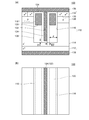
- FIG. 1 is a diagram for explaining a semiconductor device 100 according to a first embodiment.
- FIG. 1A shows an enlarged cross-sectional view of a main part of the semiconductor device 100 (hereinafter simply referred to as a cross-sectional view), and
- FIG. 1B shows an enlarged plan view of the main part of the semiconductor device 100 (hereinafter simply referred to as a plan view). ).
- the source electrode 136, the source region 130, and the contact region 132 are not shown for the sake of simplicity.
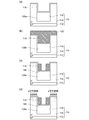
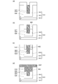
- FIG. 5 is a cross-sectional view for explaining the method for manufacturing the semiconductor device according to the first embodiment.
- 2A to 2D are process diagrams.
- FIG. 5 is a cross-sectional view for explaining the method for manufacturing the semiconductor device according to the first embodiment.
- FIG. 5 is a cross-sectional view for explaining the method for manufacturing the semiconductor device according to the first embodiment.
- 4A to 4D are process diagrams.
- FIG. 5 is a cross-sectional view for explaining the method for manufacturing the semiconductor device according to the first embodiment.
- FIG. 5A to FIG. 5D are process diagrams.
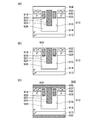
- FIG. 6 is a cross-sectional view of a semiconductor device 102 according to a second embodiment.
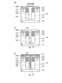
- FIG. 10 is a cross-sectional view for explaining the method for manufacturing the semiconductor device according to the second embodiment.
- FIG. 7A to FIG. 7C are process diagrams.
- FIG. 6 is a cross-sectional view of a semiconductor device 104 according to a third embodiment.
- FIG. 10 is a cross-sectional view for explaining the method for manufacturing a semiconductor device according to the third embodiment.
- FIG. 9A to FIG. 9C are process diagrams.
- FIG. 6 is a cross-sectional view of a semiconductor device 106 according to a fourth embodiment.
- FIG. 10 is a cross-sectional view for explaining the method for manufacturing a semiconductor device according to the fourth embodiment.
- FIG. 11A to FIG. 11C are process diagrams.
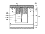
- FIG. 10 is a cross-sectional view of a semiconductor device according to a fifth embodiment.
- FIG. 10 is a cross-sectional view for explaining the method for manufacturing a semiconductor device according to the fifth embodiment.
- 13A to 13C are process diagrams. It is a figure shown in order to demonstrate the manufacturing method of the conventional semiconductor device.
- FIGS. 14D are process diagrams. It is a figure shown in order to demonstrate the manufacturing method of the conventional semiconductor device.
- FIGS. 15A to 15D are process diagrams. It is a figure shown in order to demonstrate the manufacturing method of the conventional semiconductor device.
- FIGS. 16A to 16D are process diagrams. It is a figure shown in order to demonstrate the manufacturing method of the conventional semiconductor device.
- FIGS. 17A to 17C are process diagrams. In FIG. 17C, reference numeral 938 denotes a drain electrode.
- Embodiment 1 Configuration of Semiconductor Device 100 According to Embodiment 1
- the semiconductor device 100 according to Embodiment 1 is a power MOSFET having a planar direction separation type shield gate structure in which a gate electrode and a shield electrode are separated in a planar direction.
- the semiconductor device 100 includes an n + -type first semiconductor layer 112 and an n ⁇ -type second semiconductor layer 114 having a lower concentration than the first semiconductor layer 112.
- the shield electrode 1 is separated from the side wall and bottom of the trench 116 and extends along the side wall and bottom of the trench 116. 4, a base region 128 formed on the surface of the second semiconductor layer 114 in a region where the trench 116 is not formed in plan view, and a part of the surface of the base region 128 is a trench. 116 is formed in a source region 130 (first conductivity type high concentration diffusion region) formed so as to be exposed on the side wall of 116 and a predetermined region (region in which source region 130 is not formed) on the surface of base region 128.
- source region 130 first conductivity type high concentration diffusion region
- the + -type contact region 132 is disposed directly on the surface of the shield electrode 124 and is disposed on the surface of the gate electrode 120 via the protective insulating film 134, and directly with the shield electrode 124, the source region 130, and the contact region 132.
- the source electrode 136 is connected, and the drain electrode 138 is formed on the surface of the first semiconductor layer 112.
- the insulating region 126 interposed between the gate electrode 120 and the shield electrode 124 is thicker than the gate insulating film 118.
- the thickness of the insulating region 126 between the bottom of the shield electrode 124 and the bottom of the trench 116 is D1, and the side wall of the shield electrode 124 at the depth position of the bottom of the shield electrode 124.
- the trench 116, the gate electrode 120, the base region 128, the source region 130, and the contact region 132 are all formed in a stripe shape (see FIG. 1B).
- the thickness of the first semiconductor layer 112 is 50 ⁇ m to 500 ⁇ m (for example, 350 ⁇ m), and the impurity concentration of the first semiconductor layer 112 is 1 ⁇ 10 18 cm ⁇ 3 to 1 ⁇ 10 21 cm ⁇ 3 (for example, 1 ⁇ 10 19 cm). -3 ).
- the thickness of the second semiconductor layer 114 in the region where the trench 116 is not formed is 3 ⁇ m to 50 ⁇ m (for example, 15 ⁇ m), and the impurity concentration of the second semiconductor layer 114 is 1 ⁇ 10 14 cm ⁇ 3 to 1 ⁇ 10 19 cm. -3 (for example, 1 ⁇ 10 15 cm -3 ).
- the thickness of the base region 128 is 0.5 [mu] m ⁇ 10 [mu] m (e.g. 5 [mu] m), the impurity concentration of the base region 128 is 1 ⁇ 10 16 cm -3 ⁇ 1 ⁇ 10 19 cm -3 ( e.g., 1 ⁇ 10 17 cm -3 ).
- the depth of the trench 116 is 1 ⁇ m to 20 ⁇ m (for example, 10 ⁇ m), the pitch of the trench 116 is 3 ⁇ m to 20 ⁇ m (for example, 10 ⁇ m), and the opening width of the trench 116 is 0.3 ⁇ m to 19 ⁇ m (for example, 7 ⁇ m).
- the gate insulating film 118 is made of, for example, a silicon dioxide film formed by a thermal oxidation method, and the thickness of the gate insulating film 118 is 20 nm to 200 nm (for example, 100 nm).
- the gate electrode 120 is made of, for example, low-resistance polysilicon formed by a CVD method, and the thickness of the gate electrode 120 is 0.1 ⁇ m to 5 ⁇ m (for example, 2 ⁇ m).
- the distance between the shield electrode 124 and the gate electrode 120 is 0.02 ⁇ m to 3 ⁇ m (for example, 1 ⁇ m), and the distance between the shield electrode 124 and the bottom of the trench 116 is 0.1 ⁇ m to 3 ⁇ m (for example, 2 ⁇ m).
- the distance between the shield electrode 124 and the side wall of the trench 116 at the bottom depth position is 0.1 ⁇ m to 8 ⁇ m (for example, 3 ⁇ m).
- the depth position of the upper surface of the shield electrode 124 with respect to the protective insulating film 134 is in the range of 0.01 ⁇ m to 2 ⁇ m.
- the depth of the source region 130 is 1 ⁇ m to 3 ⁇ m (for example, 2 ⁇ m), and the impurity concentration of the source region 130 is 1 ⁇ 10 18 cm ⁇ 3 to 1 ⁇ 10 20 cm ⁇ 3 (for example, 2 ⁇ 10 19 cm ⁇ 3 ). is there.
- the depth of the contact region 132 is 1 ⁇ m to 3 ⁇ m (for example, 2 ⁇ m), and the impurity concentration of the contact region 132 is 1 ⁇ 10 18 cm ⁇ 3 to 1 ⁇ 10 20 cm ⁇ 3 (for example, 2 ⁇ 10 19 cm ⁇ 3 ). is there.
- the protective insulating film 134 is made of, for example, a silicon dioxide film formed by a CVD method, and the thickness of the protective insulating film 134 is 0.5 ⁇ m to 3 ⁇ m (for example, 1 ⁇ m).
- the source electrode 136 is made of, for example, an Al film or an Al alloy film (for example, an AlSi film), and the thickness of the source electrode 136 is 1 ⁇ m to 10 ⁇ m (for example, 3 ⁇ m).
- the drain electrode 138 is formed of a laminated film in which Ti, Ni, and Au are laminated in this order, and the thickness of the drain electrode 138 is 0.2 ⁇ m to 1.5 ⁇ m (for example, 1 ⁇ m).
- the insulating region 126 interposed between the gate electrode 120 and the shield electrode 124 is thicker than the gate insulating film 118.
- the breakdown voltage between the gate electrode 120 and the shield electrode 124 can be made higher than that of the conventional semiconductor device 900.
- the semiconductor device 100 according to the first embodiment can be manufactured by a manufacturing method (a manufacturing method of a semiconductor device according to the first embodiment) having the following manufacturing process.
- a semiconductor substrate 110 having an n + -type first semiconductor layer 112 and an n ⁇ -type second semiconductor layer 114 having a lower concentration than the first semiconductor layer 112 is prepared (FIG. 2).
- an appropriate semiconductor substrate can be used.
- a semiconductor substrate in which an n ⁇ type second semiconductor layer 114 is formed on the n + type first semiconductor layer 112 by an epitaxial growth method is used. it can.
- a semiconductor substrate made of silicon is used as the semiconductor substrate 110, but a semiconductor substrate made of a material other than silicon may be used.
- a mask (not shown) having a predetermined opening is formed on the surface of the second semiconductor layer 114, and the second semiconductor is etched by using the mask.
- a predetermined first trench 116 is formed in the layer 114 (see FIG. 2B).
- a silicon oxide film 126a ′ having a predetermined thickness is formed on the surface of the second semiconductor layer 114 (including the inside of the first trench 116) by a CVD method ( (See FIG. 2 (c)).
- the thickness of the silicon oxide film 126a ′ is in the range of 0.5 ⁇ m to 5 ⁇ m, for example.
- the silicon oxide film 126a ′ other than the lower portion of the first trench 116 is removed by etching back, and the first insulating film 126a is formed so as to fill the lower portion of the first trench 116 (see FIG. 2D). .
- Gate Insulating Film Formation Step by thermal oxidation, on the surface of the upper sidewall of the first trench 116, on the surface of the first insulating film 126a and the second semiconductor layer 114 (on the upper side of the first trench 116). A silicon oxide film is formed on the side wall surface (see FIG. 3A). A silicon oxide film formed on the upper sidewall of the first trench 116 constitutes the gate insulating film 118.
- the thickness of the gate insulating film 118 is in the range of 20 nm to 200 nm, for example.
- a polysilicon layer 120 ′ is formed on the surface of the silicon oxide film by a CVD method (see FIG. 3B).
- the polysilicon layer 120 ′ is etched back to form the gate electrode 120 made of polysilicon (see FIG. 3C).
- the gate electrode layer forming step the polysilicon layer 120 ′ is etched back so that the gate electrode 120 is formed at a position spaced apart from the first trench 116 at a predetermined interval.
- a p-type impurity for example, boron
- a mask (not shown) having an opening corresponding to the contact region 132 is formed in the second semiconductor layer 114, and a p-type impurity is disposed at a higher impurity concentration and at a shallower depth position through the mask.
- boron is ion-implanted (see FIG. 3D).
- a mask (not shown) having an opening corresponding to the source region 130 is formed on the surface of the second semiconductor layer 114, and n-type impurities (for example, phosphorus) are ion-implanted through the mask (FIG. 4 (a).)
- n-type impurities for example, phosphorus
- the base region 128, the source region 130, and the contact region 132 are formed by thermally diffusing the p-type impurity and the n-type impurity ion-implanted into the second semiconductor layer 114 (see FIG. 4B).
- Second Trench Formation Step a mask (not shown) having an opening is formed in the central portion of the first insulating film 126a, and the central portion of the first insulating film 126a is etched by using the mask. By removing, the second trench 140 is formed in the first trench 116 (see FIG. 4C).
- the opening width of the second trench 140 is equal to the interval between the two gate electrodes 120 in the first trench 116, and is, for example, in the range of 0.1 ⁇ m to 5 ⁇ m.
- the second trench 140 is formed up to the depth of the first trench 116.
- the second insulating film 126b is formed by thermal oxidation in the second trench 140 under the condition that the air gap remains in the second trench 140 (see FIG. 4D). .) At this time, the second insulating film 126 b is also formed on the region of the second semiconductor layer 114 where the first trench 116 is not formed and on the surface of the gate electrode 120. The first insulating film 126a and the second insulating film 126b form an insulating region 126, and the second insulating film 126b on the gate electrode 120 forms a protective insulating film 134.
- the second insulating film 126b is formed so that the thickness is larger than the thickness of the gate insulating film 118.
- the thickness of the second insulating film 126b is in the range of 0.2 ⁇ m to 5 ⁇ m.
- the depth of the gap 122 is in the range of 0.5 ⁇ m to 19 ⁇ m, and the opening width of the gap 122 is in the range of 0.1 ⁇ m to 5 ⁇ m.
- the thickness of the second insulating film 126b between the bottom of the gap 122 and the bottom of the first trench 116 is D1
- the side wall of the gap 122 at the depth position of the bottom of the gap 122 The thickness of the first insulating film 126a between the side wall of the first trench 116 is d
- Source and drain electrode formation step Next, the source electrode 130, the contact region 132, the shield electrode 124, and the protective insulating film 134 are directly connected to the shield electrode 124, the source region 130, and the contact region 132 on the surface. A source electrode 136 is formed. Further, the drain electrode 138 is formed on the surface of the first semiconductor layer 112 (see FIG. 5D).
- the semiconductor device 100 according to the first embodiment can be manufactured.
- the thickness of the insulating film on the bottom side of the shield electrode (second insulating film) and the insulating film on the side of the shield electrode side (first film) It becomes easy to set the thicknesses of the first insulating film and the second insulating film to arbitrary thicknesses. As a result, a semiconductor device can be manufactured with a high degree of design freedom.
- an oxide film formed by thermally oxidizing single crystal silicon and an oxide film formed by thermally oxidizing polysilicon are considered to have different film quality. That is, the ratio of SiO 2 is considered to be relatively high in an oxide film formed by thermally oxidizing single crystal silicon, whereas an oxide film formed by thermally oxidizing polysilicon is formed of SiO 2 . In addition, it is considered that the ratio of SiO X is high. Accordingly, the oxide film formed by thermally oxidizing the polysilicon of the gate electrode 120 (an oxide film between the gate electrode 120 and the shield electrode 124) is likely to vary, and the ESD between the gate electrode 120 and the shield electrode 124 is likely to occur. It is considered that the tolerance is likely to vary.
- the second insulating film 126b is formed so that the thickness is larger than the thickness of the gate insulating film 118.
- the breakdown voltage between the gate and the source can be made higher than that of the conventional semiconductor device 900.
- the thickness of the second insulating film 126b between the bottom of the gap 122 and the bottom of the first trench 116 is D1
- the gap The thickness of the first insulating film 126a between the side wall of the gap 122 and the side wall of the first trench 116 at the depth position of the bottom of 122 is d
- the side wall of the gap 122 at the depth position of the bottom of the gap 122 is D2 (see FIG. 1).
- the shield electrode 124 can be formed to a deep depth position, and the depletion layer can reach a deep position at the time of reverse bias. As a result, the breakdown voltage between the source and the drain can be increased.
- the distance from the corner of the first trench 116 where the electric field concentration is likely to occur to the gate electrode 120 can be increased, and further, the electric field can be relaxed by the first insulating film 126a and the second insulating film 126b. As a result, the breakdown voltage can be increased also from this viewpoint.
- the second trench 140 is formed up to the depth of the first trench 116 in the second trench formation step.
- the depth position of the first trench 116 is a boundary surface between the first insulating film 126a and the second semiconductor layer 114.
- the first insulating film 126a (material is an oxide film) and the second semiconductor layer 114 (silicon) are Since the materials are different, by adopting such a configuration, the etching performed in the second trench formation process can be stopped at the depth position of the first trench 116 with high accuracy, and as a result, the depth is high.
- the second trench 140 that is uniform with accuracy can be formed.
- the source electrode 136 is formed so as to be directly connected to the shield electrode 124, the source region 130, and the contact region 132.
- the contact area between 136, the source region 130, and the contact region 132 is large, and the contact resistance can be reduced.
- the first insulating film 126a is formed by the CVD method, so that the first insulating film 126a is formed at a relatively lower temperature than in the case of the thermal oxidation method.
- One insulating film 126a can be formed, and heating damage to the semiconductor substrate 110 can be reduced.
- the second insulating film 126b is formed by the thermal oxidation method, and thus the insulating film is formed even in the relatively narrow gap 122. can do.
- the semiconductor device 102 according to the second embodiment basically has the same configuration as the semiconductor device 100 according to the first embodiment, but the first embodiment is that the source electrode is connected to the source region via a metal plug. This is different from the case of the semiconductor device 100 according to the above. That is, in the semiconductor device 102 according to the second embodiment, as shown in FIG. 6, the second insulating film 126b is also formed between the source electrode 136 and the source region 130, and the second insulating film 126b A predetermined opening 142 is formed, and a metal plug 144 formed by filling the opening 142 with metal is formed.
- the semiconductor device 102 according to the second embodiment can be manufactured by a method for manufacturing a semiconductor device according to the second embodiment described below.
- the manufacturing method of the semiconductor device according to the second embodiment basically includes the same steps as the manufacturing method of the semiconductor device according to the first embodiment, but includes the metal plug formation step. It is different from the manufacturing method. That is, in the method for manufacturing the semiconductor device according to the second embodiment, the process is performed as shown in FIG. 7 between the shield electrode formation step (see FIG. 5B) and the source electrode formation step (see FIG. 5D). As shown, an opening forming step (see FIG. 7A) for forming a predetermined opening 142 in the second insulating film 126b so as to reach the base region 128, and a metal plug is formed by filling the opening 142 with metal. And a metal plug forming step for forming 144 (see FIG. 7B).
- the source electrode 136 is formed so as to be directly connected to the shield electrode 124 and to be connected to the source region 130 and the base region 128 via the metal plug 144 (see FIG. 7C). .
- the openings 142 and the metal plugs 144 are formed in a stripe shape, and the stripe width is, for example, 0.5 ⁇ m.
- a barrier metal (not shown) is formed on the inner surface of the opening 142, and the metal plug 144 is formed by filling the opening 142 with a predetermined metal through the barrier metal.
- the predetermined metal is, for example, tungsten.
- the manufacturing method of the semiconductor device according to the second embodiment is different from the manufacturing method of the semiconductor device according to the first embodiment in that it includes a metal plug forming step.
- the shield electrode forming process is included in the subsequent stage of the gate electrode forming process, the insulating film is not formed on the shield electrode 124 before the source electrode forming process. Therefore, an insulating film removing process for removing the insulating film is not necessary, and the process for connecting the shield electrode 124 and the source electrode 136 can be simplified.
- an opening forming step of forming a predetermined opening in the second insulating film 126b between the shield electrode forming step and the source electrode forming step, and the opening 142 A metal plug forming step of filling the inside with metal to form a metal plug 144.
- the metal plug 144 is directly connected to the shield electrode 124 and is connected to the source region 130 and the base region 128. Since the source electrode 136 is formed so as to be connected through the semiconductor device, a large opening is formed by removing a large amount of the protective insulating film as in the method of manufacturing a semiconductor device in which the source electrode is in direct contact with the source region. Therefore, a miniaturized semiconductor device can be manufactured. As a result, the semiconductor device manufacturing method according to the second embodiment can manufacture a semiconductor device that meets the demand for cost reduction and miniaturization of electronic equipment.
- the semiconductor device manufacturing method according to the second embodiment includes the same steps as the semiconductor device manufacturing method according to the first embodiment except that the method includes a metal plug forming step. It has the effect applicable among the effects which the manufacturing method of an apparatus has.
- the semiconductor device 104 according to the third embodiment basically has the same configuration as the semiconductor device 100 according to the first embodiment, but the shape of the trench is different from that of the semiconductor device 100 according to the first embodiment. That is, in the trench 116 of the semiconductor device 104 according to the third embodiment, as shown in FIG. 8, the depth of the trench 116 in the region where the shield electrode 124 is formed is seen in plan view. It is deeper than the depth of the trench 116 in the region where the shield electrode 124 is not formed.
- the semiconductor device 104 according to the third embodiment can be manufactured by a method for manufacturing a semiconductor device according to the third embodiment described below.
- the manufacturing method of the semiconductor device according to the third embodiment basically includes the same steps as the manufacturing method of the semiconductor device according to the first embodiment, but the depth of the second trench formed in the second trench forming step is performed. This is different from the semiconductor device manufacturing method according to the first embodiment. That is, in the second trench formation step of the method for manufacturing a semiconductor device according to the third embodiment, as shown in FIG. 9A, the second trench 140a is deeper than the depth of the first trench 116. Form.
- the second insulating film 126b is also formed on the surface of the second trench 140a formed at a depth position deeper than the depth position of the first trench 116 (FIG. 9 ( See b). Thereafter, a shield electrode layer forming step is performed (see FIG. 9C).
- the semiconductor device manufacturing method according to the third embodiment differs from the semiconductor device manufacturing method according to the first embodiment in that the depth of the second trench formed in the second trench formation step is different from that in the first embodiment.
- an insulating film for example, a gate insulating film and a protective film
- Insulating film is not formed. Therefore, an insulating film removing process for removing the insulating film is not necessary, and the process for connecting the shield electrode 124 and the source electrode 136 can be simplified.
- the second trench 140a is formed to a depth position deeper than the depth position of the first trench 116, so that the shield electrode 124 can be formed to a deep depth position. Therefore, the manufactured semiconductor device can reach the depletion layer to a deep position at the time of reverse bias, and can increase the breakdown voltage between the source and the drain.
- the second trench 140a is formed to a depth position deeper than the depth position of the first trench 116. Since etching is stopped at the depth of the trench 116, it is not necessary to control the etching with high accuracy, and a semiconductor device can be manufactured relatively easily.
- the depth of the trench 116 in the region where the shield electrode 124 is formed in a plan view is the region where the shield electrode 124 is not formed in a plan view. Therefore, the shield electrode 124 can be formed to a deep depth position. Therefore, at the time of reverse bias, the depletion layer can reach a deep position, and the breakdown voltage between the source and the drain can be increased.
- the semiconductor device manufacturing method according to the third embodiment includes the same steps as the semiconductor device manufacturing method according to the first embodiment except for the depth of the second trench formed in the second trench forming step.
- the semiconductor device manufacturing method according to the first embodiment has a corresponding effect.
- the semiconductor device 106 according to the fourth embodiment basically has the same configuration as that of the semiconductor device 100 according to the first embodiment, but is different from the semiconductor device 100 according to the first embodiment in that it further includes a p-type diffusion region. Is different. That is, in the semiconductor device 106 according to the fourth embodiment, as shown in FIG. 10, the p-type diffusion region 148 (second conductivity type diffusion region) is formed so as to be in contact with the bottom of the trench 116. Note that the impurity concentration of the p-type diffusion region 148 is higher than the impurity concentration of the base region 128.
- the semiconductor device 106 according to Embodiment 4 can be manufactured by a method for manufacturing a semiconductor device according to Embodiment 4 described below.
- the semiconductor device manufacturing method according to the fourth embodiment basically includes the same steps as those of the semiconductor device manufacturing method according to the first embodiment, but includes the p-type diffusion region forming step. It differs from the manufacturing method of the device. That is, in the method for manufacturing a semiconductor device according to the fourth embodiment, as shown in FIGS. 11A and 11B, the second trench formation step (see FIG. 4C) and the second insulating film. A p-type diffusion region forming step for forming the p-type diffusion region 148 so as to be in contact with the bottom of the second trench 140 during the formation step (see FIG. 4D) (second conductivity type diffusion region forming step). Further included.
- a p-type impurity is introduced into the bottom of the second trench 140 (see FIG. 11A) to activate the p-type impurity.
- a p-type diffusion region 148 is formed.
- a second insulating film forming step see FIG. 11B
- a shield electrode forming step see FIG. 11C
- the manufacturing method of the semiconductor device according to the fourth embodiment is different from the manufacturing method of the semiconductor device according to the first embodiment in that it includes the p-type diffusion region forming step, but the manufacturing method of the semiconductor device according to the first embodiment.
- an insulating film for example, a gate insulating film and a protective insulating film
- an insulating film removing process for removing the insulating film is not necessary, and the process for connecting the shield electrode 124 and the source electrode 136 can be simplified.
- the p-type diffusion region 148 is formed so as to be in contact with the bottom of the second trench 140 between the second trench formation step and the second insulating film formation step. Since the p-type diffusion region forming step is included, the depletion layer can reach a deep position at the time of reverse bias. As a result, the breakdown voltage between the source and the drain can be increased.
- the semiconductor device manufacturing method according to the fourth embodiment includes the same steps as those of the semiconductor device manufacturing method according to the first embodiment except that the p-type diffusion region forming step is included. This has a corresponding effect among the effects of the semiconductor device manufacturing method.
- the semiconductor device 108 according to the fifth embodiment basically has the same configuration as the semiconductor device 100 according to the first embodiment, but the shape of the shield electrode is different from that of the semiconductor device 100 according to the first embodiment. That is, in the semiconductor device 106 according to the fourth embodiment, as shown in FIG. 12, the shield electrode 124a has a side surface with a narrow bottom taper shape.
- the semiconductor device 108 according to the fifth embodiment can be manufactured by the method for manufacturing a semiconductor device according to the fifth embodiment described below.
- the semiconductor device manufacturing method according to the fifth embodiment basically includes the same steps as the semiconductor device manufacturing method according to the first embodiment, but the shape of the second trench formed in the second trench forming step is the embodiment. 1 is different from the method for manufacturing a semiconductor device according to No. 1. That is, in the second trench formation step of the method for manufacturing a semiconductor device according to the fifth embodiment, as shown in FIG. 13A, a trench having a narrow bottom tapered side surface is formed as the second trench 140b. In the second trench forming step, a trench having a side surface having a narrow bottom taper is formed by adjusting the etching gas conditions (type of etching gas, temperature, etc.).
- the gap 122a also has a narrow taper side surface (specifically, the gap 122a is formed in order to form the second insulating film 126b along the surface of the second trench 140b.
- the shape is a triangular shape that protrudes downward (see FIG. 13B).
- the shield electrode 124a having a narrow taper-shaped side surface can be formed by embedding polysilicon in the gap 122a (see FIG. 13C).
- the manufacturing method of the semiconductor device according to the fifth embodiment is different from the manufacturing method of the semiconductor device according to the first embodiment, although the shape of the second trench formed in the second trench forming step is different from that of the first embodiment.
- an insulating film for example, a gate insulating film and a protective insulating film
- an insulating film removing process for removing the insulating film is not necessary, and the process for connecting the shield electrode 124 and the source electrode 136 can be simplified.
- a trench having a narrow bottom tapered side surface is formed as the second trench 140b.
- Such a voltage is higher than the voltage applied to the lower part of the shield electrode 124a. Therefore, the potential change of the drain electrode can be moderated when the switch is turned off, and as a result, the surge voltage can be reduced when the switch is turned off.
- the manufacturing method of the semiconductor device according to the fifth embodiment includes the same steps as the manufacturing method of the semiconductor device according to the first embodiment except for the shape of the second trench formed in the second trench forming step. It has the effect applicable among the effects which the manufacturing method of the semiconductor device which concerns on Embodiment 1 has.
- the first insulating film is formed by the CVD method, but the present invention is not limited to this.
- the first insulating film may be formed by a thermal oxidation method.
- the second insulating film is formed by the thermal oxidation method, but the present invention is not limited to this.
- the second insulating film may be formed by a CVD method.
- the second trench is formed up to the depth of the first trench, and in the second trench formation step of the third embodiment, although the second trench is formed to a depth position deeper than the depth position of the first trench, the present invention is not limited to this. In the second trench formation step, the second trench may be formed to a depth position shallower than the depth position of the first trench.
- the present invention is not limited to this.
- the second trench is formed to a depth position shallower than the depth position of the first trench.
- the n-type impurity is introduced after the p-type impurity is introduced, but the present invention is not limited to this.
- the p-type impurity may be introduced after the n-type impurity is introduced.
- the impurities are activated collectively after introducing the p-type impurity and the n-type impurity.
- the present invention is not limited to this. It may be activated each time each impurity is introduced.
- the base region 128, the source region 130, and the contact region 132 are formed before forming the shield electrode, but the present invention is not limited to this. After forming the shield electrode, the base region 128, the source region 130, and the contact region 132 may be formed.
- the trench (first trench), the gate electrode, and the shield electrode are each formed in a stripe shape when seen in a plan view, but the present invention is not limited to this.
- Each of the trench (first trench), the gate electrode, and the shield electrode may be formed in a lattice shape or a dot shape (columnar shape when viewed three-dimensionally) when seen in a plan view.
- polysilicon is used as the material of the shield electrode, but the present invention is not limited to this.
- a metal may be used as the material of the shield electrode.
- the MOSFET has been described as an example of the semiconductor device, but the present invention is not limited to this.
- the present invention can be variously applied to devices other than MOSFETs without departing from the spirit of the present invention.
Landscapes
- Electrodes Of Semiconductors (AREA)
- Engineering & Computer Science (AREA)
- Manufacturing & Machinery (AREA)
Abstract
本発明の半導体装置の製造方法は、半導体基体準備工程と、第1トレンチ形成工程と、第1絶縁膜126aを形成する第1絶縁膜形成工程と、ゲート絶縁膜形成工程と、ゲート電極形成工程と、第1絶縁膜126aの中央部を除去して第1トレンチ116内に第2トレンチ140を形成する第2トレンチ形成工程と、第2トレンチ内に空隙122が残存する条件で第2トレンチ140の内部に第2絶縁膜126bを形成する第2絶縁膜形成工程と、空隙122内にシールド電極124を形成するシールド電極形成工程と、ソース電極を形成するソース電極形成工程とをこの順序で含む。 本発明の半導体装置の製造方法によれば、シールド電極とソース電極との接続を取るための工程が簡略化でき、かつ、高い設計自由度で半導体装置を製造することが可能となる。
Description
本発明は、半導体装置の製造方法及び半導体装置に関する。
従来、ゲート電極とシールド電極とが平面方向に分離された平面方向分離型のシールドゲート構造を備える半導体装置が知られている(例えば、特許文献1参照。)。
従来の半導体装置900は、図14~図17に示すように、以下の方法(従来の半導体装置の製造方法)を実施することにより製造することができる。すなわち、従来の半導体装置900は、(1)n+型の第1半導体層912及び第1半導体層912よりも低濃度のn-型の第2半導体層914を有する半導体基体910を準備する半導体基体準備工程(図14(a)参照。)と、(2)第2半導体層914に所定の第1トレンチ916を形成する第1トレンチ形成工程(図14(b)参照。)と、(3)第1トレンチ916内の中央に第1空隙922が残存する条件で熱酸化法により第1トレンチ916の内部に第1絶縁膜926を形成する第1絶縁膜形成工程(図14(c)参照。)と、(4)第1空隙922内にシールド電極924を形成するシールド電極形成工程(図14(d)及び図15(a)参照。)と、(5)第1トレンチ916の下部を残して第1絶縁膜926をエッチングバックする第1絶縁膜エッチングバック工程(図15(b)参照。)と、(6)シールド電極924の側壁、第1トレンチ916の上部の側壁及びエッチングバックされた第1絶縁膜926の上面で構成される凹部950内に第2空隙952が残存する条件で凹部950の内部にゲート絶縁膜918を形成するゲート絶縁膜形成工程(図15(c)参照。)と、(7)第2空隙952内にゲート電極920を形成するゲート電極形成工程(図15(d)及び図16(a)参照。)と、(8)ベース領域928、ソース領域930(第1導電型高濃度拡散領域)、及び、p+型のコンタクト領域932を形成する不純物領域形成工程と(図16(b)~図16(d)参照。)、(9)ゲート電極920及びゲート絶縁膜918上に保護絶縁膜934を形成する保護絶縁膜形成工程(図17(a)参照。)と、(10)シールド電極924の上部に形成された絶縁膜(ゲート絶縁膜及び保護絶縁膜)を除去する絶縁膜除去工程(図17(b)参照。)と、(11)シールド電極924と電気的に接続するようにソース電極936を形成するソース電極形成工程(図17(c)参照。)とを実施することにより製造することができる。
しかしながら、従来の半導体装置の製造方法においては、シールド電極形成工程の後段にゲート電極形成工程を含むことから、ソース電極形成工程の前段までにシールド電極924の上部には絶縁膜(ゲート絶縁膜及び保護絶縁膜)が形成される(図17(a)参照。)。従って、シールド電極924とソース電極936との接続を取るためには、シールド電極924の上部に形成された絶縁膜(ゲート絶縁膜及び保護絶縁膜)を除去する絶縁膜除去工程が必要となり(図17(b)参照。)、シールド電極924とソース電極936との接続を取るための工程が煩雑になるという問題がある。
また、従来の半導体装置の製造方法においては、第1絶縁膜形成工程において、第1トレンチ916内の中央に第1空隙922が残存する条件で熱酸化法により第1トレンチ916の内部に第1絶縁膜926を形成した後(図14(c)参照。)、シールド電極形成工程において、第1空隙922内にシールド電極924を形成するため(図14(d)及び図15(a)参照。)、シールド電極底部側の絶縁膜(第1絶縁膜)の厚さとシールド電極側部側の絶縁膜(第1絶縁膜)の厚さとを任意の厚さに設定することが難しく、高い設計自由度で半導体装置を製造することが困難であるという問題もある。
そこで、本発明は、上記した問題を解決するためになされたものであり、シールド電極とソース電極との接続を取るための工程が簡略化でき、かつ、高い設計自由度で半導体装置を製造することが可能な半導体装置の製造方法を提供することを目的とする。また、そのような半導体装置の製造方法で製造された半導体装置を提供することを目的とする。
[1]本発明の半導体装置の製造方法は、ゲート電極とシールド電極とが平面方向に分離された平面方向分離型のシールドゲート構造を備える半導体装置の製造方法であって、第1導電型の第1半導体層及び当該第1半導体層よりも低濃度の第1導電型の第2半導体層を有する半導体基体を準備する半導体基体準備工程と、前記第2半導体層に所定の第1トレンチを形成する第1トレンチ形成工程と、前記第1トレンチの下部を埋めるように第1絶縁膜を形成する第1絶縁膜形成工程と、前記第1トレンチの上部の側壁にゲート絶縁膜を形成するゲート絶縁膜形成工程と、前記ゲート絶縁膜を介して、ポリシリコンからなる前記ゲート電極を形成するゲート電極形成工程と、前記第1絶縁膜の中央部をエッチングにより除去して前記第1トレンチ内に第2トレンチを形成する第2トレンチ形成工程と、前記第2トレンチ内に空隙が残存する条件で少なくとも前記第2トレンチの内部に第2絶縁膜を形成する第2絶縁膜形成工程と、前記空隙内に前記シールド電極を形成するシールド電極形成工程と、前記シールド電極と電気的に接続するようにソース電極を形成するソース電極形成工程とをこの順序で含むことを特徴とする。
[2]本発明の半導体装置の製造方法においては、前記第2絶縁膜形成工程において、厚さが前記ゲート絶縁膜の厚さよりも厚くなるように前記第2絶縁膜を形成することが好ましい。
[3]本発明の半導体装置の製造方法においては、前記第2絶縁膜形成工程において、前記空隙の底と前記第1トレンチの底との間の前記第2絶縁膜の厚さをD1とし、前記空隙の前記底の深さ位置における前記空隙の側壁と前記第1トレンチの側壁との間の前記第1絶縁膜の厚さをdとし、前記空隙の前記底の深さ位置における前記空隙の前記側壁と前記第1トレンチの前記側壁との間の前記第2絶縁膜の厚さをD2としたときに、D1≦d+D2の関係を満たすように前記第2絶縁膜を形成することが好ましい。
[4]本発明の半導体装置の製造方法においては、前記第2トレンチ形成工程において、前記第1トレンチの深さ位置まで前記第2トレンチを形成することが好ましい。
[5]本発明の半導体装置の製造方法においては、前記第2トレンチ形成工程において、前記第1トレンチの深さ位置よりも深い深さ位置まで前記第2トレンチを形成することが好ましい。
[6]本発明の半導体装置の製造方法においては、前記第2トレンチ形成工程と前記第2絶縁膜形成工程との間に、前記第2トレンチの底に接するように第2導電型拡散領域を形成する第2導電型拡散領域形成工程をさらに含むことが好ましい。
[7]本発明の半導体装置の製造方法においては、前記第2トレンチ形成工程において、前記第2トレンチとして、底狭テーパー形状の側面を有するトレンチを形成することが好ましい。
[8]本発明の半導体装置の製造方法においては、前記ゲート電極形成工程と前記第2トレンチ形成工程との間に、平面的に見て前記第1トレンチが形成されていない領域における前記第2半導体層の表面に第2導電型のベース領域を形成するベース領域形成工程と、前記ベース領域の表面に、少なくとも一部が前記第1トレンチの前記側壁に露出するように第1導電型高濃度拡散領域を形成する第1導電型高濃度拡散領域形成工程とをさらに含むことが好ましい。
[9]本発明の半導体装置の製造方法においては、前記ゲート電極形成工程と前記第2トレンチ形成工程との間に、前記ベース領域の表面の所定領域に第2導電型のコンタクト領域を形成するコンタクト領域形成工程をさらに含み、前記シールド電極形成工程と前記ソース電極形成工程との間に、平面的に見て前記第1トレンチが形成されていない領域における前記第2絶縁膜をエッチングバックにより除去する第2絶縁膜エッチングバック工程をさらに含み、前記ソース電極形成工程においては、前記シールド電極、前記第1導電型高濃度拡散領域及び前記コンタクト領域に直接接続するように前記ソース電極を形成することが好ましい。
[10]本発明の半導体装置の製造方法においては、前記シールド電極形成工程と前記ソース電極形成工程との間に、前記第2絶縁膜に所定の開口を形成する開口形成工程と、前記開口の内部に金属を充填して金属プラグを形成する金属プラグ形成工程とをさらに含み、前記ソース電極形成工程においては、前記シールド電極に直接接続し、かつ、前記第1導電型高濃度拡散領域及び前記ベース領域に前記金属プラグを介して接続するように前記ソース電極を形成することが好ましい。
[11]本発明の半導体装置の製造方法においては、前記第1絶縁膜形成工程において、CVD法によって前記第1絶縁膜を形成することが好ましい。
[12]本発明の半導体装置の製造方法においては、前記第1絶縁膜形成工程において、熱酸化法によって前記第1絶縁膜を形成することが好ましい。
[13]本発明の半導体装置の製造方法においては、前記第2絶縁膜形成工程において、CVD法によって前記第2絶縁膜を形成することが好ましい。
[14]本発明の半導体装置の製造方法においては、前記第2絶縁膜形成工程において、熱酸化法によって前記第2絶縁膜を形成することが好ましい。
[15]本発明の半導体装置は、ゲート電極とシールド電極とが平面方向に分離された平面方向分離型のシールドゲート構造を備える半導体装置であって、第1導電型の第1半導体層及び当該第1半導体層よりも低濃度の第1導電型の第2半導体層を有する半導体基体と、前記第2半導体層の表面に位置する所定のトレンチと、ポリシリコンからなり、前記トレンチの上部の側壁にゲート絶縁膜を介して形成された前記ゲート電極と、前記トレンチの中央部に、前記ゲート電極と離間した状態で形成された前記シールド電極と、前記トレンチ内において、前記ゲート電極と前記シールド電極との間に拡がり前記ゲート電極から前記シールド電極を離隔させるとともに、前記トレンチの側壁及び底に沿って拡がり前記トレンチの前記側壁及び前記底から前記シールド電極を離隔させる絶縁領域とを備え、前記ゲート電極と前記シールド電極との間に介在する前記絶縁領域の厚さが前記ゲート絶縁膜よりも厚いことを特徴とする。
本発明の半導体装置の製造方法によれば、ゲート電極形成工程の後段にシールド電極形成工程を含むため、ソース電極形成工程の前段までにシールド電極の上部には絶縁膜(例えば、ゲート絶縁膜及び保護絶縁膜)が形成されない。従って、当該絶縁膜(ゲート絶縁膜及び保護絶縁膜)を除去する絶縁膜除去工程が必要でなくなり、シールド電極とソース電極との接続を取るための工程を簡略化できる。
また、本発明の半導体装置の製造方法によれば、第1絶縁膜の中央部をエッチングにより除去して第1トレンチ内に第2トレンチを形成した後、第2トレンチ内に空隙が残存する条件で第2トレンチの内部に第2絶縁膜を形成するため、シールド電極底部側の絶縁膜(第2絶縁膜)の厚さとシールド電極側部側の絶縁膜(第1絶縁膜及び第2絶縁膜)の厚さを任意の厚さに設定することが容易となり、その結果、高い設計自由度で半導体装置を製造することができる。
本発明の半導体装置によれば、ゲート電極とシールド電極との間に介在する絶縁領域の厚さがゲート絶縁膜よりも厚いため、従来の半導体装置よりもゲート電極とシールド電極との間の耐圧を高くすることができる。
以下、本発明の半導体装置の製造方法及び半導体装置について、図に示す実施の形態に基づいて説明する。なお、各図面は模式図であり、必ずしも実際の寸法を厳密に反映したものではない。
[実施形態1]
1.実施形態1に係る半導体装置100の構成
実施形態1に係る半導体装置100は、ゲート電極とシールド電極とが平面方向に分離された平面方向分離型のシールドゲート構造を備えるパワーMOSFETである。
1.実施形態1に係る半導体装置100の構成
実施形態1に係る半導体装置100は、ゲート電極とシールド電極とが平面方向に分離された平面方向分離型のシールドゲート構造を備えるパワーMOSFETである。
実施形態1に係る半導体装置100は、図1に示すように、n+型の第1半導体層112及び当該第1半導体層112よりも低濃度のn-型の第2半導体層114を有する半導体基体110と、第2半導体層114の表面に位置する所定のトレンチ116(第1トレンチ)と、ポリシリコンからなり、トレンチ116の上部の側壁にゲート絶縁膜118を介して形成されたゲート電極120と、トレンチ116の中央部に、ゲート電極120と離間した状態で形成されたシールド電極124と、トレンチ116内において、ゲート電極120とシールド電極124との間に拡がりゲート電極120からシールド電極124を離隔させるとともに、トレンチ116の側壁及び底に沿って拡がりトレンチ116の側壁及び底からシールド電極124を離隔させる絶縁領域126と、平面的に見てトレンチ116が形成されていない領域における第2半導体層114の表面に形成されたベース領域128と、ベース領域128の表面に、一部がトレンチ116の側壁に露出するように形成されたソース領域130(第1導電型高濃度拡散領域)と、ベース領域128の表面の所定領域(ソース領域130が形成されていない領域)に形成されたp+型のコンタクト領域132と、シールド電極124の表面上に直接配置されるとともにゲート電極120の表面上に保護絶縁膜134を介して配置され、シールド電極124、ソース領域130及びコンタクト領域132と直接接続されているソース電極136と、第1半導体層112の表面上に形成されたドレイン電極138とを備える。
実施形態1に係る半導体装置100においては、ゲート電極120とシールド電極124との間に介在する絶縁領域126の厚さがゲート絶縁膜118よりも厚い。
実施形態1に係る半導体装置100においては、シールド電極124の底とトレンチ116の底との間の絶縁領域126の厚さをD1とし、シールド電極124の底の深さ位置におけるシールド電極124の側壁とトレンチ116の側壁との間の絶縁領域126の厚さ(後述する第1絶縁膜126aの厚さと後述する第2絶縁膜126bの厚さとを合計した厚さ)をd+D2としたときに、D1<d+D2の関係を満たす。
実施形態1においては、トレンチ116、ゲート電極120、ベース領域128、ソース領域130及びコンタクト領域132はいずれもストライプ状に形成されている(図1(b)参照。)。
第1半導体層112の厚さは50μm~500μm(例えば350μm)であり、第1半導体層112の不純物濃度は1×1018cm-3~1×1021cm-3(例えば1×1019cm-3)である。トレンチ116が形成されていない領域における第2半導体層114の厚さは3μm~50μm(例えば15μm)であり、第2半導体層114の不純物濃度は1×1014cm-3~1×1019cm-3(例えば1×1015cm-3)である。ベース領域128の厚さは0.5μm~10μm(例えば5μm)であり、ベース領域128の不純物濃度は1×1016cm-3~1×1019cm-3(例えば1×1017cm-3)である。
トレンチ116の深さは1μm~20μm(例えば10μm)であり、トレンチ116のピッチは3μm~20μm(例えば10μm)であり、トレンチ116の開口幅は、0.3μm~19μm(例えば7μm)である。ゲート絶縁膜118は例えば熱酸化法により形成された二酸化珪素膜からなり、ゲート絶縁膜118の厚さは20nm~200nm(例えば100nm)である。ゲート電極120は例えばCVD法により形成された低抵抗のポリシリコンからなり、ゲート電極120の厚さは0.1μm~5μm(例えば2μm)である。
シールド電極124とゲート電極120との間隔は0.02μm~3μm(例えば1μm)であり、シールド電極124とトレンチ116の底との間隔は0.1μm~3μm(例えば2μm)であり、シールド電極124の底の深さ位置におけるシールド電極124とトレンチ116の側壁との間隔は0.1μm~8μm(例えば3μm)である。また、保護絶縁膜134を基準としたときのシールド電極124の上面の深さ位置は、0.01μm~2μmの範囲内にある。
ソース領域130の深さは1μm~3μm(例えば2μm)であり、ソース領域130の不純物濃度は1×1018cm-3~1×1020cm-3(例えば2×1019cm-3)である。コンタクト領域132の深さは1μm~3μm(例えば2μm)であり、コンタクト領域132の不純物濃度は1×1018cm-3~1×1020cm-3(例えば2×1019cm-3)である。保護絶縁膜134は例えばCVD法により形成された二酸化珪素膜からなり、保護絶縁膜134の厚さは0.5μm~3μm(例えば1μm)である。
ソース電極136は例えばAl膜又はAl合金膜(例えばAlSi膜)からなり、ソース電極136の厚さは1μm~10μm(例えば3μm)である。ドレイン電極138はTi、Ni、Auがこの順序で積層された積層膜からなり、ドレイン電極138の厚さは0.2μm~1.5μm(例えば1μm)である。
2.実施形態1に係る半導体装置100の効果
実施形態1に係る半導体装置100によれば、ゲート電極120とシールド電極124との間に介在する絶縁領域126の厚さがゲート絶縁膜118よりも厚いため、従来の半導体装置900よりもゲート電極120とシールド電極124との間の耐圧を高くすることができる。
実施形態1に係る半導体装置100によれば、ゲート電極120とシールド電極124との間に介在する絶縁領域126の厚さがゲート絶縁膜118よりも厚いため、従来の半導体装置900よりもゲート電極120とシールド電極124との間の耐圧を高くすることができる。
3.実施形態1に係る半導体装置の製造方法
実施形態1に係る半導体装置100は、以下に示す製造工程を有する製造方法(実施形態1に係る半導体装置の製造方法)により製造することができる。
実施形態1に係る半導体装置100は、以下に示す製造工程を有する製造方法(実施形態1に係る半導体装置の製造方法)により製造することができる。
(1)半導体基体準備工程
まず、n+型の第1半導体層112及び当該第1半導体層112よりも低濃度のn-型の第2半導体層114を有する半導体基体110を準備する(図2(a)参照。)。半導体基体110としては適宜の半導体基体を用いることができ、例えばn+型の第1半導体層112上にエピタキシャル成長法によってn-型の第2半導体層114を形成してなる半導体基体を用いることができる。なお、実施形態1においては、半導体基体110として、シリコンからなる半導体基体を用いるが、シリコン以外の材料からなる半導体基体を用いてもよい。
まず、n+型の第1半導体層112及び当該第1半導体層112よりも低濃度のn-型の第2半導体層114を有する半導体基体110を準備する(図2(a)参照。)。半導体基体110としては適宜の半導体基体を用いることができ、例えばn+型の第1半導体層112上にエピタキシャル成長法によってn-型の第2半導体層114を形成してなる半導体基体を用いることができる。なお、実施形態1においては、半導体基体110として、シリコンからなる半導体基体を用いるが、シリコン以外の材料からなる半導体基体を用いてもよい。
(2)第1トレンチ形成工程
次に、第2半導体層114の表面上に、所定の開口を有するマスク(図示せず。)を形成し、当該マスクを用いてエッチングすることにより、第2半導体層114に所定の第1トレンチ116を形成する(図2(b)参照。)。
次に、第2半導体層114の表面上に、所定の開口を有するマスク(図示せず。)を形成し、当該マスクを用いてエッチングすることにより、第2半導体層114に所定の第1トレンチ116を形成する(図2(b)参照。)。
(3)第1絶縁膜形成工程
次に、第2半導体層114の表面上(第1トレンチ116の内部も含む)に、CVD法により、所定の厚さのシリコン酸化膜126a’を形成する(図2(c)参照。)。シリコン酸化膜126a’の厚さは、例えば0.5μm~5μmの範囲内にある。次に、エッチングバックにより第1トレンチ116の下部以外の部分の当該シリコン酸化膜126a’を取り除き、第1トレンチ116の下部を埋めるように第1絶縁膜126aを形成する(図2(d)参照。)。
次に、第2半導体層114の表面上(第1トレンチ116の内部も含む)に、CVD法により、所定の厚さのシリコン酸化膜126a’を形成する(図2(c)参照。)。シリコン酸化膜126a’の厚さは、例えば0.5μm~5μmの範囲内にある。次に、エッチングバックにより第1トレンチ116の下部以外の部分の当該シリコン酸化膜126a’を取り除き、第1トレンチ116の下部を埋めるように第1絶縁膜126aを形成する(図2(d)参照。)。
(4)ゲート絶縁膜形成工程
次に、熱酸化法によって、第1トレンチ116の上部の側壁の表面上、第1絶縁膜126a及び第2半導体層114の表面上(第1トレンチ116の上部の側壁の表面上を含む。)にシリコン酸化膜を形成する(図3(a)参照。)。第1トレンチ116の上部の側壁に形成されたシリコン酸化膜がゲート絶縁膜118を構成する。ゲート絶縁膜118の厚さは、例えば20nm~200nmの範囲内にある。
次に、熱酸化法によって、第1トレンチ116の上部の側壁の表面上、第1絶縁膜126a及び第2半導体層114の表面上(第1トレンチ116の上部の側壁の表面上を含む。)にシリコン酸化膜を形成する(図3(a)参照。)。第1トレンチ116の上部の側壁に形成されたシリコン酸化膜がゲート絶縁膜118を構成する。ゲート絶縁膜118の厚さは、例えば20nm~200nmの範囲内にある。
(5)ゲート電極形成工程
次に、CVD法によって、シリコン酸化膜の表面上にポリシリコン層120’を形成する(図3(b)参照。)。次に、ポリシリコン層120’をエッチングバックすることにより、ポリシリコンからなるゲート電極120を形成する(図3(c)参照。)。ゲート電極層形成工程においては、第1トレンチ116内において、所定の間隔で離間した位置にゲート電極120が形成されるようにポリシリコン層120’をエッチバックする。
次に、CVD法によって、シリコン酸化膜の表面上にポリシリコン層120’を形成する(図3(b)参照。)。次に、ポリシリコン層120’をエッチングバックすることにより、ポリシリコンからなるゲート電極120を形成する(図3(c)参照。)。ゲート電極層形成工程においては、第1トレンチ116内において、所定の間隔で離間した位置にゲート電極120が形成されるようにポリシリコン層120’をエッチバックする。
(6)ベース領域128、ソース領域130及びコンタクト領域132形成工程
次に、平面的に見て第1トレンチ116が形成されていない領域における第2半導体層114の表面にp型不純物(例えば、ボロン)をイオン注入する。次に、第2半導体層114にコンタクト領域132に対応する開口を有するマスク(図示せず。)を形成し、当該マスクを介してより高い不純物濃度、かつ、より浅い深さ位置にp型不純物(例えば、ボロン)をイオン注入する(図3(d)参照。)。次に、第2半導体層114の表面にソース領域130に対応する開口を有するマスク(図示せず。)を形成し、当該マスクを介してn型不純物(例えば、リン)をイオン注入する(図4(a)参照。)。次に、第2半導体層114にイオン注入したp型不純物及びn型不純物を熱拡散することにより、ベース領域128、ソース領域130及びコンタクト領域132を形成する(図4(b)参照。)。
次に、平面的に見て第1トレンチ116が形成されていない領域における第2半導体層114の表面にp型不純物(例えば、ボロン)をイオン注入する。次に、第2半導体層114にコンタクト領域132に対応する開口を有するマスク(図示せず。)を形成し、当該マスクを介してより高い不純物濃度、かつ、より浅い深さ位置にp型不純物(例えば、ボロン)をイオン注入する(図3(d)参照。)。次に、第2半導体層114の表面にソース領域130に対応する開口を有するマスク(図示せず。)を形成し、当該マスクを介してn型不純物(例えば、リン)をイオン注入する(図4(a)参照。)。次に、第2半導体層114にイオン注入したp型不純物及びn型不純物を熱拡散することにより、ベース領域128、ソース領域130及びコンタクト領域132を形成する(図4(b)参照。)。
(7)第2トレンチ形成工程
次に、第1絶縁膜126aの中央部に開口を有するマスク(図示せず。)を形成し、当該マスクを用いて第1絶縁膜126aの中央部をエッチングにより除去して第1トレンチ116内に第2トレンチ140を形成する(図4(c)参照。)。第2トレンチ140の開口幅は、第1トレンチ116内における2つのゲート電極120の間隔と等しく、例えば、0.1μm~5μmの範囲内にある。
次に、第1絶縁膜126aの中央部に開口を有するマスク(図示せず。)を形成し、当該マスクを用いて第1絶縁膜126aの中央部をエッチングにより除去して第1トレンチ116内に第2トレンチ140を形成する(図4(c)参照。)。第2トレンチ140の開口幅は、第1トレンチ116内における2つのゲート電極120の間隔と等しく、例えば、0.1μm~5μmの範囲内にある。
第2トレンチ形成工程においては、第1トレンチ116の深さ位置まで第2トレンチ140を形成する。
(8)第2絶縁膜形成工程
次に、第2トレンチ140内に空隙が残存する条件で第2トレンチ140の内部に熱酸化法によって第2絶縁膜126bを形成する(図4(d)参照。)。このとき、第2半導体層114における第1トレンチ116が形成されていない領域及びゲート電極120の表面上にも第2絶縁膜126bが形成される。なお、第1絶縁膜126aと第2絶縁膜126bとで絶縁領域126を構成し、ゲート電極120上の第2絶縁膜126bは保護絶縁膜134を構成する。
次に、第2トレンチ140内に空隙が残存する条件で第2トレンチ140の内部に熱酸化法によって第2絶縁膜126bを形成する(図4(d)参照。)。このとき、第2半導体層114における第1トレンチ116が形成されていない領域及びゲート電極120の表面上にも第2絶縁膜126bが形成される。なお、第1絶縁膜126aと第2絶縁膜126bとで絶縁領域126を構成し、ゲート電極120上の第2絶縁膜126bは保護絶縁膜134を構成する。
第2絶縁膜形成工程においては、厚さがゲート絶縁膜118の厚さよりも厚くなるように第2絶縁膜126bを形成する。第2絶縁膜126bの厚さは、0.2μm~5μmの範囲内にある。また、空隙122の深さは、0.5μm~19μmの範囲内にあり、空隙122の開口幅は、0.1μm~5μmの範囲内にある。
第2絶縁膜形成工程においては、空隙122の底と第1トレンチ116の底との間の第2絶縁膜126bの厚さをD1とし、空隙122の底の深さ位置における空隙122の側壁と第1トレンチ116の側壁との間の第1絶縁膜126aの厚さをdとし、空隙122の底の深さ位置における空隙122の側壁と第1トレンチ116の側壁との間の第2絶縁膜126bの厚さをD2としたときに、D1<d+D2の関係を満たす(符号D1,D2,dについては、図1参照。)。
(9)シールド電極形成工程
次に、半導体基体110の第2半導体層114側の表面全域にポリシリコン層124’を形成する(図5(a)参照。)。次に、エッチングバックにより空隙122の内部以外の領域のポリシリコン層124’を除去しシールド電極124を形成する(図5(b)参照。)。
次に、半導体基体110の第2半導体層114側の表面全域にポリシリコン層124’を形成する(図5(a)参照。)。次に、エッチングバックにより空隙122の内部以外の領域のポリシリコン層124’を除去しシールド電極124を形成する(図5(b)参照。)。
(10)第2絶縁膜エッチングバック工程
次に、平面的に見て第1トレンチ116が形成されていない領域における第2絶縁膜126bを第2半導体層114の表面に達するまでエッチングバックにより除去する(図5(c)参照。)。なお、このとき、ゲート電極120上の保護絶縁膜134も第2半導体層114の表面に達するまで除去する。
次に、平面的に見て第1トレンチ116が形成されていない領域における第2絶縁膜126bを第2半導体層114の表面に達するまでエッチングバックにより除去する(図5(c)参照。)。なお、このとき、ゲート電極120上の保護絶縁膜134も第2半導体層114の表面に達するまで除去する。
(11)ソース電極及びドレイン電極形成工程
次に、ソース領域130、コンタクト領域132、シールド電極124及び保護絶縁膜134の表面上に、シールド電極124、ソース領域130及びコンタクト領域132に直接接続するようにソース電極136を形成する。また、第1半導体層112の表面上にドレイン電極138を形成する(図5(d)参照。)。
次に、ソース領域130、コンタクト領域132、シールド電極124及び保護絶縁膜134の表面上に、シールド電極124、ソース領域130及びコンタクト領域132に直接接続するようにソース電極136を形成する。また、第1半導体層112の表面上にドレイン電極138を形成する(図5(d)参照。)。
このようにして実施形態1に係る半導体装置100を製造することができる。
4.実施形態1に係る半導体装置の製造方法の効果
実施形態1に係る半導体装置の製造方法によれば、ゲート電極形成工程の後段にシールド電極形成工程を含むため、ソース電極形成工程の前段までにシールド電極124の上部には絶縁膜(例えば、ゲート絶縁膜及び保護絶縁膜)が形成されない。従って、当該絶縁膜を除去する絶縁膜除去工程が必要でなくなり、シールド電極124とソース電極136との接続を取るための工程を簡略化できる。
実施形態1に係る半導体装置の製造方法によれば、ゲート電極形成工程の後段にシールド電極形成工程を含むため、ソース電極形成工程の前段までにシールド電極124の上部には絶縁膜(例えば、ゲート絶縁膜及び保護絶縁膜)が形成されない。従って、当該絶縁膜を除去する絶縁膜除去工程が必要でなくなり、シールド電極124とソース電極136との接続を取るための工程を簡略化できる。
また、実施形態1に係る半導体装置の製造方法によれば、第1絶縁膜126aの中央部をエッチングにより除去して第1トレンチ116内に第2トレンチ140を形成した後、第2トレンチ140内に空隙が残存する条件で第2トレンチ140の内部に第2絶縁膜126bを形成するため、シールド電極底部側の絶縁膜(第2絶縁膜)の厚さとシールド電極側部側の絶縁膜(第1絶縁膜及び第2絶縁膜)の厚さを任意の厚さに設定することが容易となり、その結果、高い設計自由度で半導体装置を製造することができる。
なお、一般に、単結晶シリコンを熱酸化させて形成された酸化膜と、ポリシリコンを熱酸化させて形成した酸化膜とは、膜質が異なると考えられる。すなわち、単結晶シリコンを熱酸化させて形成された酸化膜にはSiO2の割合が比較的高いと考えられるのに対して、ポリシリコンを熱酸化させて形成した酸化膜には、SiO2の他にSiOXの割合が高いものと考えられる。従って、ゲート電極120のポリシリコンを熱酸化させて形成した酸化膜(ゲート電極120とシールド電極124との間の酸化膜)にばらつきが生じ易く、ゲート電極120とシールド電極124との間のESD耐量にばらつきが生じやすいと考えられる。
しかしながら、実施形態1に係る半導体装置の製造方法によれば、上記したようにシールド電極底部側の絶縁膜(第2絶縁膜)の厚さとシールド電極側部側の絶縁膜(第1絶縁膜及び第2絶縁膜)の厚さを任意の厚さに設定することが容易であるため、ESD耐量のばらつきの少ない半導体装置を製造することができる。
しかしながら、実施形態1に係る半導体装置の製造方法によれば、上記したようにシールド電極底部側の絶縁膜(第2絶縁膜)の厚さとシールド電極側部側の絶縁膜(第1絶縁膜及び第2絶縁膜)の厚さを任意の厚さに設定することが容易であるため、ESD耐量のばらつきの少ない半導体装置を製造することができる。
また、実施形態1に係る半導体装置の製造方法によれば、第2絶縁膜形成工程においては、厚さがゲート絶縁膜118の厚さよりも厚くなるように第2絶縁膜126bを形成するため、従来の半導体装置900よりもゲート・ソース間の耐圧を高くすることができる。
また、実施形態1に係る半導体装置の製造方法は、第2絶縁膜形成工程において、空隙122の底と第1トレンチ116の底との間の第2絶縁膜126bの厚さをD1とし、空隙122の底の深さ位置における空隙122の側壁と第1トレンチ116の側壁との間の第1絶縁膜126aの厚さをdとし、空隙122の底の深さ位置における空隙122の側壁と第1トレンチ116の側壁との間の第2絶縁膜126bの厚さをD2としたときに、D1<d+D2の関係を満たすように第2絶縁膜126bを形成する(図1参照。)。
このような方法とすることにより、(1)シールド電極124を深い深さ位置まで形成することができ、逆バイアス時において、深い位置まで空乏層を到達させることができる。その結果、ソース・ドレイン間の耐圧を高くすることできる。また、(2)電界集中が起こり易い第1トレンチ116の角部からゲート電極120までの距離を長くでき、さらには、第1絶縁膜126a及び第2絶縁膜126bで電界を緩和することができる結果、この観点からも耐圧を高くできる。
このような方法とすることにより、(1)シールド電極124を深い深さ位置まで形成することができ、逆バイアス時において、深い位置まで空乏層を到達させることができる。その結果、ソース・ドレイン間の耐圧を高くすることできる。また、(2)電界集中が起こり易い第1トレンチ116の角部からゲート電極120までの距離を長くでき、さらには、第1絶縁膜126a及び第2絶縁膜126bで電界を緩和することができる結果、この観点からも耐圧を高くできる。
また、実施形態1に係る半導体装置の製造方法は、第2トレンチ形成工程においては、第1トレンチ116の深さ位置まで第2トレンチ140を形成する。第1トレンチ116の深さ位置は、第1絶縁膜126aと第2半導体層114との境界面であり、第1絶縁膜126a(材質は酸化膜)と第2半導体層114(シリコン)とは材質が異なることから、このような構成とすることにより、第2トレンチ形成工程で行われるエッチングを高い精度で第1トレンチ116の深さ位置で停止させることができ、その結果、深さが高い精度で均一な第2トレンチ140を形成することができる。
また、実施形態1に係る半導体装置の製造方法によれば、ソース電極形成工程においては、シールド電極124、ソース領域130及びコンタクト領域132に直接接続するようにソース電極136を形成するため、ソース電極136とソース領域130及びコンタクト領域132との接触面積が大きく、コンタクト抵抗を小さくすることができる。
また、実施形態1に係る半導体装置の製造方法によれば、第1絶縁膜形成工程においては、CVD法によって第1絶縁膜126aを形成するため、熱酸化法の場合よりも比較的低温で第1絶縁膜126aを形成することができ、半導体基体110に対する加熱のダメージを低減することができる。
また、実施形態1に係る半導体装置の製造方法によれば、第2絶縁膜形成工程においては、熱酸化法によって第2絶縁膜126bを形成するため、比較的狭い空隙122内でも絶縁膜を形成することができる。
[実施形態2]
実施形態2に係る半導体装置102は、基本的には実施形態1に係る半導体装置100と同様の構成を有するが、ソース電極が金属プラグを介してソース領域と接続されている点で実施形態1に係る半導体装置100の場合とは異なる。すなわち、実施形態2に係る半導体装置102においては、図6に示すように、第2絶縁膜126bがソース電極136とソース領域130との間にも形成されており、第2絶縁膜126bには所定の開口142が形成されており、当該開口142の内部に金属を充填してなる金属プラグ144が形成されている。
実施形態2に係る半導体装置102は、基本的には実施形態1に係る半導体装置100と同様の構成を有するが、ソース電極が金属プラグを介してソース領域と接続されている点で実施形態1に係る半導体装置100の場合とは異なる。すなわち、実施形態2に係る半導体装置102においては、図6に示すように、第2絶縁膜126bがソース電極136とソース領域130との間にも形成されており、第2絶縁膜126bには所定の開口142が形成されており、当該開口142の内部に金属を充填してなる金属プラグ144が形成されている。
実施形態2に係る半導体装置102は、以下に説明する実施形態2に係る半導体装置の製造方法により製造することができる。
実施形態2に係る半導体装置の製造方法は、基本的には実施形態1に係る半導体装置の製造方法と同様の工程を含むが、金属プラグ形成工程を含む点で実施形態1に係る半導体装置の製造方法とは異なる。すなわち、実施形態2に係る半導体装置の製造方法においては、シールド電極形成工程(図5(b)参照。)とソース電極形成工程(図5(d)参照。)との間に、図7に示すように、第2絶縁膜126bに所定の開口142をベース領域128に達するように形成する開口形成工程(図7(a)参照。)と、開口142の内部に金属を充填して金属プラグ144を形成する金属プラグ形成工程(図7(b)参照。)とをさらに含む。
ソース電極形成工程においては、シールド電極124に直接接続し、かつ、ソース領域130及びベース領域128に金属プラグ144を介して接続するようにソース電極136を形成する(図7(c)参照。)。
開口142及び金属プラグ144はストライプ状に形成されており、ストライプ幅は、例えば0.5μmである。開口142の内表面には、バリアメタル(図示せず)が形成されており、金属プラグ144は、当該バリアメタルを介して所定の金属が開口142の内部に充填されてなる。所定の金属は、例えば、タングステンである。
このように、実施形態2に係る半導体装置の製造方法は、金属プラグ形成工程を含む点で実施形態1に係る半導体装置の製造方法とは異なるが、実施形態1に係る半導体装置の製造方法と同様に、ゲート電極形成工程の後段にシールド電極形成工程を含むため、ソース電極形成工程の前段までにシールド電極124の上部には絶縁膜が形成されない。従って、当該絶縁膜を除去する絶縁膜除去工程が必要でなくなり、シールド電極124とソース電極136との接続を取るための工程を簡略化できる。
また、実施形態2に係る半導体装置の製造方法によれば、シールド電極形成工程とソース電極形成工程との間に、第2絶縁膜126bに所定の開口を形成する開口形成工程と、開口142の内部に金属を充填して金属プラグ144を形成する金属プラグ形成工程とをさらに含み、ソース電極形成工程においては、シールド電極124に直接接続し、かつ、ソース領域130及びベース領域128に金属プラグ144を介して接続するようにソース電極136を形成するため、ソース電極がソース領域と直接コンタクトしている半導体装置の製造方法の場合のように、保護絶縁膜を大量に除去して大きな開口を形成する必要がなく、微細化された半導体装置を製造することができる。その結果、実施形態2に係る半導体装置の製造方法は、電子機器の低コスト化及び小型化の要請に適う半導体装置を製造することができる。
なお、実施形態2に係る半導体装置の製造方法は、金属プラグ形成工程を含む点以外の点においては実施形態1に係る半導体装置の製造方法と同様の工程を含むため、実施形態1に係る半導体装置の製造方法が有する効果のうち該当する効果を有する。
[実施形態3]
実施形態3に係る半導体装置104は、基本的には実施形態1に係る半導体装置100と同様の構成を有するが、トレンチの形状が実施形態1に係る半導体装置100の場合とは異なる。すなわち、実施形態3に係る半導体装置104のトレンチ116においては、図8に示すように、平面的に見てシールド電極124が形成されている領域におけるトレンチ116の深さが、平面的に見てシールド電極124が形成されていない領域におけるトレンチ116の深さよりも深い。
実施形態3に係る半導体装置104は、基本的には実施形態1に係る半導体装置100と同様の構成を有するが、トレンチの形状が実施形態1に係る半導体装置100の場合とは異なる。すなわち、実施形態3に係る半導体装置104のトレンチ116においては、図8に示すように、平面的に見てシールド電極124が形成されている領域におけるトレンチ116の深さが、平面的に見てシールド電極124が形成されていない領域におけるトレンチ116の深さよりも深い。
実施形態3に係る半導体装置104は、以下に説明する実施形態3に係る半導体装置の製造方法により製造することができる。
実施形態3に係る半導体装置の製造方法は、基本的には実施形態1に係る半導体装置の製造方法と同様の工程を含むが、第2トレンチ形成工程で形成する第2トレンチの深さが実施形態1に係る半導体装置の製造方法とは異なる。すなわち、実施形態3に係る半導体装置の製造方法の第2トレンチ形成工程においては、図9(a)に示すように、第1トレンチ116の深さ位置よりも深い深さ位置まで第2トレンチ140aを形成する。
第2絶縁膜形成工程においては、第1トレンチ116の深さ位置よりも深い深さ位置に形成された第2トレンチ140aの表面上にも第2絶縁膜126bが形成されている(図9(b)参照。)。
その後、シールド電極層形成工程を実施する(図9(c)参照。)。
その後、シールド電極層形成工程を実施する(図9(c)参照。)。
このように、実施形態3に係る半導体装置の製造方法は、第2トレンチ形成工程で形成する第2トレンチの深さが実施形態1に係る半導体装置の製造方法とは異なるが、実施形態1に係る半導体装置の製造方法と同様に、ゲート電極形成工程の後段にシールド電極形成工程を含むため、ソース電極形成工程の前段までにシールド電極124の上部には絶縁膜(例えば、ゲート絶縁膜及び保護絶縁膜)が形成されない。従って、当該絶縁膜を除去する絶縁膜除去工程が必要でなくなり、シールド電極124とソース電極136との接続を取るための工程を簡略化できる。
また、実施形態3に係る半導体装置の製造方法によれば、第2トレンチ形成工程においては、第1トレンチ116の深さ位置よりも深い深さ位置まで第2トレンチ140aを形成するため、シールド電極124を深い深さ位置まで形成することができる。従って、製造された半導体装置は、逆バイアス時において、深い位置まで空乏層を到達させることができ、ソース・ドレイン間の耐圧を高くすることできる。
また、実施形態3に係る半導体装置の製造方法によれば、第2トレンチ形成工程においては、第1トレンチ116の深さ位置よりも深い深さ位置まで第2トレンチ140aを形成するため、第1トレンチ116の深さ位置でエッチングを停止させるために高い精度でエッチングをコントロールする必要がなく、比較的容易に半導体装置を製造することができる。
また、実施形態3に係る半導体装置104によれば、平面的に見てシールド電極124が形成されている領域におけるトレンチ116の深さが、平面的に見てシールド電極124が形成されていない領域におけるトレンチ116の深さよりも深いことから、シールド電極124を深い深さ位置まで形成することができる。従って、逆バイアス時において、深い位置まで空乏層を到達させることができ、ソース・ドレイン間の耐圧を高くすることできる。
なお、実施形態3に係る半導体装置の製造方法は、第2トレンチ形成工程で形成する第2トレンチの深さ以外の点においては実施形態1に係る半導体装置の製造方法と同様の工程を含むため、実施形態1に係る半導体装置の製造方法が有する効果のうち該当する効果を有する。
[実施形態4]
実施形態4に係る半導体装置106は、基本的には実施形態1に係る半導体装置100と同様の構成を有するが、p型拡散領域をさらに備える点で実施形態1に係る半導体装置100の場合とは異なる。すなわち、実施形態4に係る半導体装置106においては、図10に示すように、トレンチ116の底に接するようにp型拡散領域148(第2導電型拡散領域)が形成されている。なお、p型拡散領域148の不純物濃度は、ベース領域128の不純物濃度よりも高い。
実施形態4に係る半導体装置106は、基本的には実施形態1に係る半導体装置100と同様の構成を有するが、p型拡散領域をさらに備える点で実施形態1に係る半導体装置100の場合とは異なる。すなわち、実施形態4に係る半導体装置106においては、図10に示すように、トレンチ116の底に接するようにp型拡散領域148(第2導電型拡散領域)が形成されている。なお、p型拡散領域148の不純物濃度は、ベース領域128の不純物濃度よりも高い。
実施形態4に係る半導体装置106は、以下に説明する実施形態4に係る半導体装置の製造方法により製造することができる。
実施形態4に係る半導体装置の製造方法は、基本的には実施形態1に係る半導体装置の製造方法と同様の工程を含むが、p型拡散領域形成工程を含む点で実施形態1に係る半導体装置の製造方法とは異なる。すなわち、実施形態4に係る半導体装置の製造方法においては、図11(a)及び図11(b)に示すように、第2トレンチ形成工程(図4(c)参照。)と第2絶縁膜形成工程(図4(d)参照。)との間に、第2トレンチ140の底に接するようにp型拡散領域148を形成するp型拡散領域形成工程(第2導電型拡散領域形成工程)をさらに含む。
具体的には、第2トレンチ形成工程(図4(c)参照。)実施後、第2トレンチ140の底にp型不純物を導入し(図11(a)参照。)、p型不純物を活性化することでp型拡散領域148を形成する。その後、第2絶縁膜形成工程(図11(b)参照。)及びシールド電極形成工程(図11(c)参照。)を実施する。
このように、実施形態4に係る半導体装置の製造方法は、p型拡散領域形成工程を含む点で実施形態1に係る半導体装置の製造方法とは異なるが、実施形態1に係る半導体装置の製造方法と同様に、ゲート電極形成工程の後段にシールド電極形成工程を含むため、ソース電極形成工程の前段までにシールド電極124の上部には絶縁膜(例えば、ゲート絶縁膜及び保護絶縁膜)が形成されない。従って、当該絶縁膜を除去する絶縁膜除去工程が必要でなくなり、シールド電極124とソース電極136との接続を取るための工程を簡略化できる。
また、実施形態4に係る半導体装置の製造方法によれば、第2トレンチ形成工程と第2絶縁膜形成工程との間に、第2トレンチ140の底に接するようにp型拡散領域148を形成するp型拡散領域形成工程を含むため、逆バイアス時において、深い位置まで空乏層を到達させることができる。その結果、ソース・ドレイン間の耐圧を高くすることできる。
なお、実施形態4に係る半導体装置の製造方法は、p型拡散領域形成工程を含む点以外の点においては実施形態1に係る半導体装置の製造方法と同様の工程を含むため、実施形態1に係る半導体装置の製造方法が有する効果のうち該当する効果を有する。
[実施形態5]
実施形態5に係る半導体装置108は、基本的には実施形態1に係る半導体装置100と同様の構成を有するが、シールド電極の形状が実施形態1に係る半導体装置100の場合とは異なる。すなわち、実施形態4に係る半導体装置106においては、図12に示すように、シールド電極124aが底狭テーパー形状の側面を有する。
実施形態5に係る半導体装置108は、基本的には実施形態1に係る半導体装置100と同様の構成を有するが、シールド電極の形状が実施形態1に係る半導体装置100の場合とは異なる。すなわち、実施形態4に係る半導体装置106においては、図12に示すように、シールド電極124aが底狭テーパー形状の側面を有する。
実施形態5に係る半導体装置108は、以下に説明する実施形態5に係る半導体装置の製造方法により製造することができる。
実施形態5に係る半導体装置の製造方法は、基本的には実施形態1に係る半導体装置の製造方法と同様の工程を含むが、第2トレンチ形成工程において形成する第2トレンチの形状が実施形態1に係る半導体装置の製造方法とは異なる。すなわち、実施形態5に係る半導体装置の製造方法の第2トレンチ形成工程においては、図13(a)に示すように、第2トレンチ140bとして、底狭テーパー形状の側面を有するトレンチを形成する。
第2トレンチ形成工程においては、エッチングガスの条件(エッチングガスの種類、温度等)を調整することによって底狭テーパー形状の側面を有するトレンチを形成する。
第2トレンチ形成工程においては、エッチングガスの条件(エッチングガスの種類、温度等)を調整することによって底狭テーパー形状の側面を有するトレンチを形成する。
その後、第2絶縁膜形成工程においては、第2トレンチ140bの表面に沿って第2絶縁膜126bを形成するため、空隙122aも底狭テーパー形状の側面を有する(具体的には、空隙122aの形状は、下に凸となる三角形形状になる。)(図13(b)参照。)。
その後、シールド電極形成工程においては、上記した空隙122aにポリシリコンを埋め込むことにより底狭テーパー形状の側面を有するシールド電極124aを形成することができる(図13(c)参照。)。
このように、実施形態5に係る半導体装置の製造方法は、第2トレンチ形成工程において形成する第2トレンチの形状が実施形態1に係る半導体装置の製造方法とは異なるが、実施形態1に係る半導体装置の製造方法と同様に、ゲート電極形成工程の後段にシールド電極形成工程を含むため、ソース電極形成工程の前段までにシールド電極124の上部には絶縁膜(例えば、ゲート絶縁膜及び保護絶縁膜)が形成されない。従って、当該絶縁膜を除去する絶縁膜除去工程が必要でなくなり、シールド電極124とソース電極136との接続を取るための工程を簡略化できる。
また、実施形態5に係る半導体装置の製造方法によれば、第2トレンチ形成工程においては、第2トレンチ140bとして、底狭テーパー形状の側面を有するトレンチを形成するため、シールド電極124aの上部にかかる電圧がシールド電極124aの下部にかかる電圧よりも高くなる。従って、スイッチオフ時にドレイン電極の電位変化を緩やかにすることができ、その結果、スイッチオフ時にサージ電圧を低減することができる。
なお、実施形態5に係る半導体装置の製造方法は、第2トレンチ形成工程において形成する第2トレンチの形状以外の点においては実施形態1に係る半導体装置の製造方法と同様の工程を含むため、実施形態1に係る半導体装置の製造方法が有する効果のうち該当する効果を有する。
以上、本発明を上記の実施形態に基づいて説明したが、本発明は上記の実施形態に限定されるものではない。その趣旨を逸脱しない範囲において種々の態様において実施することが可能であり、例えば、次のような変形も可能である。
(1)上記実施形態において記載した構成要素の数、材質、形状、位置、大きさ等は例示であり、本発明の効果を損なわない範囲において変更することが可能である。
(2)上記各実施形態においては、CVD法によって第1絶縁膜を形成したが、本発明はこれに限定されるものではない。熱酸化法によって第1絶縁膜を形成してもよい。
(3)上記各実施形態においては、熱酸化法によって第2絶縁膜を形成したが、本発明はこれに限定されるものではない。CVD法によって第2絶縁膜を形成してもよい。
(4)上記実施形態1,2,4及び5の第2トレンチ形成工程においては、第1トレンチの深さ位置まで第2トレンチを形成し、上記実施形態3の第2トレンチ形成工程においては、第1トレンチの深さ位置よりも深い深さ位置まで第2トレンチを形成したが、本発明はこれに限定されるものではない。第2トレンチ形成工程においては、第1トレンチの深さ位置よりも浅い深さ位置まで第2トレンチを形成してもよい。
(5)上記各実施形態の第2絶縁膜形成工程において、D1<d+D2の関係を満たすように第2絶縁膜を形成したが、本発明はこれに限定されるものではない。第2絶縁膜形成工程において、D1=d+D2の関係を満たすように第2絶縁膜を形成ししてもよい。この場合には、第2トレンチ形成工程において、第1トレンチの深さ位置よりも浅い深さ位置まで第2トレンチを形成する。
(6)上記各実施形態においては、p型不純物を導入した後n型不純物を導入したが、本発明はこれに限定されるものではない。n型不純物を導入した後p型不純物を導入してもよい。
(7)上記各実施形態においては、p型不純物及びn型不純物を導入した後一括して不純物を活性化したが、本発明はこれに限定されるものではない。各不純物を導入するたびに活性化してもよい。
(8)上記各実施形態においては、シールド電極を形成する前にベース領域128、ソース領域130及びコンタクト領域132を形成したが、本発明はこれに限定されるものではない。シールド電極を形成した後にベース領域128、ソース領域130及びコンタクト領域132を形成してもよい。
(9)上記各実施形態においては、トレンチ(第1トレンチ)、ゲート電極及びシールド電極をそれぞれ、平面的に見てストライプ状に形成したが、本発明はこれに限定されるものではない。トレンチ(第1トレンチ)、ゲート電極及びシールド電極をそれぞれ、平面的に見て格子状や点状(立体的に見て柱状)に形成してもよい。
(10)上記各実施形態においては、シールド電極の材料としてポリシリコンを用いたが、本発明はこれに限定されるものではない。シールド電極の材料として金属を用いてもよい。
(11)上記各実施形態においては、半導体装置として、MOSFETを例にして説明したが、本発明はこれに限定されるものではない。本発明は、MOSFET以外の他のデバイスにも本発明の趣旨を逸脱しない範囲で種々に適用可能である。
100,102,104,106,108,900…半導体装置、110,910…半導体基体、112,912…第1半導体層、114,914…第2半導体層、116,116a、916…第1トレンチ(トレンチ)、118,918…ゲート絶縁膜、126a'…シリコン酸化膜、120,920…ゲート電極、120',124’…ポリシリコン層、122,122a…空隙、124,124a、924…シールド電極、126…絶縁領域、126a,926…第1絶縁膜、126b…第2絶縁膜、128,928…ベース領域、130,930…ソース領域、132,932…コンタクト領域、134,134a,934…保護絶縁膜、136,936…ソース電極、138,938…ドレイン電極、140,140a…第2トレンチ、142…開口、144…金属プラグ、148…p型拡散領域、922…第1空隙、950…凹部、952…第2空隙
Claims (15)
- ゲート電極とシールド電極とが平面方向に分離された平面方向分離型のシールドゲート構造を備える半導体装置の製造方法であって、
第1導電型の第1半導体層及び当該第1半導体層よりも低濃度の第1導電型の第2半導体層を有する半導体基体を準備する半導体基体準備工程と、
前記第2半導体層に所定の第1トレンチを形成する第1トレンチ形成工程と、
前記第1トレンチの下部を埋めるように第1絶縁膜を形成する第1絶縁膜形成工程と、
前記第1トレンチの上部の側壁にゲート絶縁膜を形成するゲート絶縁膜形成工程と、
前記ゲート絶縁膜を介して、ポリシリコンからなる前記ゲート電極を形成するゲート電極形成工程と、
前記第1絶縁膜の中央部をエッチングにより除去して前記第1トレンチ内に第2トレンチを形成する第2トレンチ形成工程と、
前記第2トレンチ内に空隙が残存する条件で少なくとも前記第2トレンチの内部に第2絶縁膜を形成する第2絶縁膜形成工程と、
前記空隙内に前記シールド電極を形成するシールド電極形成工程と、
前記シールド電極と電気的に接続するようにソース電極を形成するソース電極形成工程とをこの順序で含むことを特徴とする半導体装置の製造方法。 - 前記第2絶縁膜形成工程においては、厚さが前記ゲート絶縁膜の厚さよりも厚くなるように前記第2絶縁膜を形成することを特徴とする請求項1に記載の半導体装置の製造方法。
- 前記第2絶縁膜形成工程において、前記空隙の底と前記第1トレンチの底との間の前記第2絶縁膜の厚さをD1とし、前記空隙の前記底の深さ位置における前記空隙の側壁と前記第1トレンチの側壁との間の前記第1絶縁膜の厚さをdとし、前記空隙の前記底の深さ位置における前記空隙の前記側壁と前記第1トレンチの前記側壁との間の前記第2絶縁膜の厚さをD2としたときに、D1≦d+D2の関係を満たすように前記第2絶縁膜を形成することを特徴とする請求項1又は2に記載の半導体装置の製造方法。
- 前記第2トレンチ形成工程においては、前記第1トレンチの深さ位置まで前記第2トレンチを形成することを特徴とする請求項1~3のいずれかに記載の半導体装置の製造方法。
- 前記第2トレンチ形成工程においては、前記第1トレンチの深さ位置よりも深い深さ位置まで前記第2トレンチを形成することを特徴とする請求項1~3のいずれかに記載の半導体装置の製造方法。
- 前記第2トレンチ形成工程と前記第2絶縁膜形成工程との間に、前記第2トレンチの底に接するように第2導電型拡散領域を形成する第2導電型拡散領域形成工程をさらに含むことを特徴とする請求項1~5のいずれかに記載の半導体装置の製造方法。
- 前記第2トレンチ形成工程においては、前記第2トレンチとして、底狭テーパー形状の側面を有するトレンチを形成することを特徴とする請求項1~6のいずれかに記載の半導体装置の製造方法。
- 前記ゲート電極形成工程と前記第2トレンチ形成工程との間に、平面的に見て前記第1トレンチが形成されていない領域における前記第2半導体層の表面に第2導電型のベース領域を形成するベース領域形成工程と、前記ベース領域の表面に、少なくとも一部が前記第1トレンチの前記側壁に露出するように第1導電型高濃度拡散領域を形成する第1導電型高濃度拡散領域形成工程とをさらに含むことを特徴とする請求項1~7のいずれかに記載の半導体装置の製造方法。
- 前記ゲート電極形成工程と前記第2トレンチ形成工程との間に、前記ベース領域の表面の所定領域に第2導電型のコンタクト領域を形成するコンタクト領域形成工程をさらに含み、
前記シールド電極形成工程と前記ソース電極形成工程との間に、平面的に見て前記第1トレンチが形成されていない領域における前記第2絶縁膜をエッチングバックにより除去する第2絶縁膜エッチングバック工程をさらに含み、
前記ソース電極形成工程においては、前記シールド電極、前記第1導電型高濃度拡散領域及び前記コンタクト領域に直接接続するように前記ソース電極を形成することを特徴とする請求項8に記載の半導体装置の製造方法。 - 前記シールド電極形成工程と前記ソース電極形成工程との間に、前記第2絶縁膜に所定の開口を形成する開口形成工程と、前記開口の内部に金属を充填して金属プラグを形成する金属プラグ形成工程とをさらに含み、
前記ソース電極形成工程においては、前記シールド電極に直接接続し、かつ、前記第1導電型高濃度拡散領域及び前記ベース領域に前記金属プラグを介して接続するように前記ソース電極を形成することを特徴とする請求項8に記載の半導体装置の製造方法。 - 前記第1絶縁膜形成工程においては、CVD法によって前記第1絶縁膜を形成することを特徴とする請求項1~10のいずれかに記載の半導体装置の製造方法。
- 前記第1絶縁膜形成工程においては、熱酸化法によって前記第1絶縁膜を形成することを特徴とする請求項1~10のいずれかに記載の半導体装置の製造方法。
- 前記第2絶縁膜形成工程においては、CVD法によって前記第2絶縁膜を形成することを特徴とする請求項1~12のいずれかに記載の半導体装置の製造方法。
- 前記第2絶縁膜形成工程においては、熱酸化法によって前記第2絶縁膜を形成することを特徴とする請求項1~12のいずれかに記載の半導体装置の製造方法。
- ゲート電極とシールド電極とが平面方向に分離された平面方向分離型のシールドゲート構造を備える半導体装置であって、
第1導電型の第1半導体層及び当該第1半導体層よりも低濃度の第1導電型の第2半導体層を有する半導体基体と、
前記第2半導体層の表面に位置する所定のトレンチと、
ポリシリコンからなり、前記トレンチの上部の側壁にゲート絶縁膜を介して形成された前記ゲート電極と、
前記トレンチの中央部に、前記ゲート電極と離間した状態で形成された前記シールド電極と、
前記トレンチ内において、前記ゲート電極と前記シールド電極との間に拡がり前記ゲート電極から前記シールド電極を離隔させるとともに、前記トレンチの側壁及び底に沿って拡がり前記トレンチの前記側壁及び前記底から前記シールド電極を離隔させる絶縁領域と、
前記シールド電極と電気的に接続されているソース電極とを備え、
前記ゲート電極と前記シールド電極との間に介在する前記絶縁領域の厚さが前記ゲート絶縁膜よりも厚いことを特徴とする半導体装置。
Priority Applications (6)
| Application Number | Priority Date | Filing Date | Title |
|---|---|---|---|
| PCT/JP2016/060855 WO2017168733A1 (ja) | 2016-03-31 | 2016-03-31 | 半導体装置の製造方法及び半導体装置 |
| US16/086,609 US10707343B2 (en) | 2016-03-31 | 2016-03-31 | Method of manufacturing semiconductor device and semiconductor device |
| JP2017544799A JP6519894B2 (ja) | 2016-03-31 | 2016-03-31 | 半導体装置の製造方法及び半導体装置 |
| CN201680082427.8A CN108701715B (zh) | 2016-03-31 | 2016-03-31 | 半导体装置的制造方法以及半导体装置 |
| TW106109823A TWI632621B (zh) | 2016-03-31 | 2017-03-23 | 半導體裝置及其製造方法 |
| NL2018616A NL2018616B1 (en) | 2016-03-31 | 2017-03-30 | Method of manufacturing semiconductor device and semiconductor device |
Applications Claiming Priority (1)
| Application Number | Priority Date | Filing Date | Title |
|---|---|---|---|
| PCT/JP2016/060855 WO2017168733A1 (ja) | 2016-03-31 | 2016-03-31 | 半導体装置の製造方法及び半導体装置 |
Publications (1)
| Publication Number | Publication Date |
|---|---|
| WO2017168733A1 true WO2017168733A1 (ja) | 2017-10-05 |
Family
ID=59683993
Family Applications (1)
| Application Number | Title | Priority Date | Filing Date |
|---|---|---|---|
| PCT/JP2016/060855 Ceased WO2017168733A1 (ja) | 2016-03-31 | 2016-03-31 | 半導体装置の製造方法及び半導体装置 |
Country Status (6)
| Country | Link |
|---|---|
| US (1) | US10707343B2 (ja) |
| JP (1) | JP6519894B2 (ja) |
| CN (1) | CN108701715B (ja) |
| NL (1) | NL2018616B1 (ja) |
| TW (1) | TWI632621B (ja) |
| WO (1) | WO2017168733A1 (ja) |
Cited By (4)
| Publication number | Priority date | Publication date | Assignee | Title |
|---|---|---|---|---|
| JP2019140152A (ja) * | 2018-02-06 | 2019-08-22 | 株式会社豊田中央研究所 | 半導体装置 |
| JP2024009226A (ja) * | 2020-09-11 | 2024-01-19 | 株式会社東芝 | 半導体装置 |
| JP2024503772A (ja) * | 2021-12-15 | 2024-01-29 | 蘇州東微半導体股▲ふん▼有限公司 | Igbtデバイス |
| JP2024035357A (ja) * | 2022-09-02 | 2024-03-14 | ルネサスエレクトロニクス株式会社 | 半導体装置およびその製造方法 |
Families Citing this family (12)
| Publication number | Priority date | Publication date | Assignee | Title |
|---|---|---|---|---|
| JP7261567B2 (ja) | 2018-11-26 | 2023-04-20 | 株式会社Screenホールディングス | 基板処理方法および基板処理装置 |
| CN111261702A (zh) * | 2018-12-03 | 2020-06-09 | 珠海格力电器股份有限公司 | 沟槽型功率器件及其形成方法 |
| CN109378344A (zh) * | 2018-12-11 | 2019-02-22 | 张家港凯思半导体有限公司 | 一种超低功耗半导体功率器件及其制备方法 |
| CN112435928B (zh) * | 2019-08-26 | 2023-12-29 | 无锡先瞳半导体科技有限公司 | 一种屏蔽栅功率器件及其制备方法 |
| JP7270575B2 (ja) * | 2020-04-15 | 2023-05-10 | 株式会社東芝 | 半導体装置 |
| CN111477550B (zh) * | 2020-05-26 | 2022-11-18 | 上海华虹宏力半导体制造有限公司 | 一种功率半导体器件及其制作方法 |
| CN111785641B (zh) * | 2020-08-26 | 2024-02-02 | 上海华虹宏力半导体制造有限公司 | 一种半导体器件的制造方法 |
| CN111785642B (zh) * | 2020-08-26 | 2023-03-21 | 上海华虹宏力半导体制造有限公司 | 一种半导体器件的制造方法 |
| CN112164648A (zh) * | 2020-09-29 | 2021-01-01 | 上海华虹宏力半导体制造有限公司 | 半导体器件的制备方法 |
| CN114975099B (zh) * | 2022-01-06 | 2025-08-19 | 上海华虹宏力半导体制造有限公司 | 一种屏蔽栅mosfet器件及其制作方法 |
| CN114188410A (zh) * | 2022-02-17 | 2022-03-15 | 绍兴中芯集成电路制造股份有限公司 | 屏蔽栅沟槽型功率mosfet器件 |
| CN116314269A (zh) * | 2023-03-23 | 2023-06-23 | 江苏临德半导体有限公司 | 降低栅极电荷的半导体器件及其制作方法 |
Citations (4)
| Publication number | Priority date | Publication date | Assignee | Title |
|---|---|---|---|---|
| JP2007165380A (ja) * | 2005-12-09 | 2007-06-28 | Toshiba Corp | 半導体装置及びその製造方法 |
| JP2010153864A (ja) * | 2008-12-23 | 2010-07-08 | Power Integrations Inc | 半導体ダイ上に製造されるパワートランジスタデバイス |
| JP2012064641A (ja) * | 2010-09-14 | 2012-03-29 | Toshiba Corp | 半導体装置 |
| US20130240984A1 (en) * | 2012-03-14 | 2013-09-19 | Taiwan Semiconductor Manufacturing Company, Ltd. | Transistor and method of manufacturing the same |
Family Cites Families (27)
| Publication number | Priority date | Publication date | Assignee | Title |
|---|---|---|---|---|
| JPH07249770A (ja) * | 1994-03-10 | 1995-09-26 | Toshiba Corp | 半導体装置及びその製造方法 |
| JP4903055B2 (ja) | 2003-12-30 | 2012-03-21 | フェアチャイルド・セミコンダクター・コーポレーション | パワー半導体デバイスおよびその製造方法 |
| US7385248B2 (en) * | 2005-08-09 | 2008-06-10 | Fairchild Semiconductor Corporation | Shielded gate field effect transistor with improved inter-poly dielectric |
| US7633120B2 (en) * | 2006-08-08 | 2009-12-15 | Alph & Omega Semiconductor, Ltd. | Inverted-trench grounded-source field effect transistor (FET) structure using highly conductive substrates |
| JP2007081424A (ja) * | 2006-11-15 | 2007-03-29 | Mitsubishi Electric Corp | トレンチ構造を有する半導体装置及びその製造方法 |
| US7998808B2 (en) * | 2008-03-21 | 2011-08-16 | International Rectifier Corporation | Semiconductor device fabrication using spacers |
| JP5420225B2 (ja) * | 2008-10-29 | 2014-02-19 | ルネサスエレクトロニクス株式会社 | 半導体装置およびその製造方法 |
| US8252647B2 (en) * | 2009-08-31 | 2012-08-28 | Alpha & Omega Semiconductor Incorporated | Fabrication of trench DMOS device having thick bottom shielding oxide |
| JP2011134837A (ja) * | 2009-12-24 | 2011-07-07 | Sanyo Electric Co Ltd | 半導体装置の製造方法 |
| US8648413B2 (en) * | 2009-12-28 | 2014-02-11 | Force Mos Technology Co., Ltd. | Super-junction trench MOSFET with multiple trenched source-body contacts |
| JP5740108B2 (ja) * | 2010-07-16 | 2015-06-24 | 株式会社東芝 | 半導体装置 |
| US7977742B1 (en) * | 2010-08-20 | 2011-07-12 | Monolithic Power Systems, Inc. | Trench-gate MOSFET with capacitively depleted drift region |
| JP2012204529A (ja) * | 2011-03-24 | 2012-10-22 | Toshiba Corp | 半導体装置及びその製造方法 |
| US8829603B2 (en) * | 2011-08-18 | 2014-09-09 | Alpha And Omega Semiconductor Incorporated | Shielded gate trench MOSFET package |
| JP2013062344A (ja) * | 2011-09-13 | 2013-04-04 | Toshiba Corp | 半導体装置およびその製造方法 |
| JP2013069852A (ja) | 2011-09-22 | 2013-04-18 | Toshiba Corp | 半導体装置 |
| CN103137698B (zh) * | 2011-11-23 | 2016-04-27 | 力士科技股份有限公司 | 一种金属氧化物半导体场效应晶体管及制造方法 |
| US9443972B2 (en) * | 2011-11-30 | 2016-09-13 | Infineon Technologies Austria Ag | Semiconductor device with field electrode |
| JP2013125827A (ja) * | 2011-12-14 | 2013-06-24 | Toshiba Corp | 半導体装置およびその製造方法 |
| US8878287B1 (en) * | 2012-04-12 | 2014-11-04 | Micrel, Inc. | Split slot FET with embedded drain |
| US8975662B2 (en) | 2012-06-14 | 2015-03-10 | Infineon Technologies Austria Ag | Method of manufacturing a semiconductor device using an impurity source containing a metallic recombination element and semiconductor device |
| US20140167152A1 (en) * | 2012-12-13 | 2014-06-19 | International Rectifier Corporation | Reduced Gate Charge Trench Field-Effect Transistor |
| US8951867B2 (en) * | 2012-12-21 | 2015-02-10 | Alpha And Omega Semiconductor Incorporated | High density trench-based power MOSFETs with self-aligned active contacts and method for making such devices |
| US9543396B2 (en) | 2013-12-13 | 2017-01-10 | Power Integrations, Inc. | Vertical transistor device structure with cylindrically-shaped regions |
| US9324823B2 (en) * | 2014-08-15 | 2016-04-26 | Infineon Technologies Austria Ag | Semiconductor device having a tapered gate structure and method |
| US9831335B2 (en) * | 2015-02-20 | 2017-11-28 | Shindengen Electric Manufacturing Co., Ltd. | Semiconductor device |
| CN105514170A (zh) * | 2016-01-14 | 2016-04-20 | 晶科华兴集成电路(深圳)有限公司 | 一种功率金属氧化物半导体场效应晶体管及其制作方法 |
-
2016
- 2016-03-31 WO PCT/JP2016/060855 patent/WO2017168733A1/ja not_active Ceased
- 2016-03-31 US US16/086,609 patent/US10707343B2/en active Active
- 2016-03-31 CN CN201680082427.8A patent/CN108701715B/zh active Active
- 2016-03-31 JP JP2017544799A patent/JP6519894B2/ja active Active
-
2017
- 2017-03-23 TW TW106109823A patent/TWI632621B/zh active
- 2017-03-30 NL NL2018616A patent/NL2018616B1/en active
Patent Citations (4)
| Publication number | Priority date | Publication date | Assignee | Title |
|---|---|---|---|---|
| JP2007165380A (ja) * | 2005-12-09 | 2007-06-28 | Toshiba Corp | 半導体装置及びその製造方法 |
| JP2010153864A (ja) * | 2008-12-23 | 2010-07-08 | Power Integrations Inc | 半導体ダイ上に製造されるパワートランジスタデバイス |
| JP2012064641A (ja) * | 2010-09-14 | 2012-03-29 | Toshiba Corp | 半導体装置 |
| US20130240984A1 (en) * | 2012-03-14 | 2013-09-19 | Taiwan Semiconductor Manufacturing Company, Ltd. | Transistor and method of manufacturing the same |
Cited By (7)
| Publication number | Priority date | Publication date | Assignee | Title |
|---|---|---|---|---|
| JP2019140152A (ja) * | 2018-02-06 | 2019-08-22 | 株式会社豊田中央研究所 | 半導体装置 |
| JP2024009226A (ja) * | 2020-09-11 | 2024-01-19 | 株式会社東芝 | 半導体装置 |
| JP7581468B2 (ja) | 2020-09-11 | 2024-11-12 | 株式会社東芝 | 半導体装置 |
| JP2024503772A (ja) * | 2021-12-15 | 2024-01-29 | 蘇州東微半導体股▲ふん▼有限公司 | Igbtデバイス |
| JP7482571B2 (ja) | 2021-12-15 | 2024-05-14 | 蘇州東微半導体股▲ふん▼有限公司 | Igbtデバイス |
| JP2024035357A (ja) * | 2022-09-02 | 2024-03-14 | ルネサスエレクトロニクス株式会社 | 半導体装置およびその製造方法 |
| JP7821705B2 (ja) | 2022-09-02 | 2026-02-27 | ルネサスエレクトロニクス株式会社 | 半導体装置の製造方法 |
Also Published As
| Publication number | Publication date |
|---|---|
| NL2018616A (en) | 2017-10-05 |
| CN108701715A (zh) | 2018-10-23 |
| CN108701715B (zh) | 2021-04-27 |
| US10707343B2 (en) | 2020-07-07 |
| US20190097041A1 (en) | 2019-03-28 |
| JPWO2017168733A1 (ja) | 2018-04-05 |
| TW201737356A (zh) | 2017-10-16 |
| TWI632621B (zh) | 2018-08-11 |
| NL2018616B1 (en) | 2018-02-01 |
| JP6519894B2 (ja) | 2019-05-29 |
Similar Documents
| Publication | Publication Date | Title |
|---|---|---|
| JP6519894B2 (ja) | 半導体装置の製造方法及び半導体装置 | |
| JP6367514B2 (ja) | 半導体装置の製造方法及び半導体装置 | |
| JP6341074B2 (ja) | 半導体装置の製造方法 | |
| CN108496252B (zh) | 功率半导体装置以及功率半导体装置的制造方法 | |
| JP2016092257A (ja) | 炭化珪素半導体装置およびその製造方法 | |
| CN108292682B (zh) | 半导体装置以及半导体装置的制造方法 | |
| JP6159471B2 (ja) | 炭化珪素半導体装置及びその製造方法 | |
| WO2015174197A1 (ja) | 半導体装置および半導体装置の製造方法 | |
| JP5616720B2 (ja) | 半導体装置およびその製造方法 | |
| TWI574405B (zh) | Silicon carbide semiconductor device, method for manufacturing silicon carbide semiconductor device, and design method of silicon carbide semiconductor device | |
| JP2021002548A (ja) | 半導体装置および半導体装置の製造方法 | |
| JP2008135474A (ja) | 半導体装置 | |
| JP2018061055A (ja) | 半導体装置 | |
| JP2012142487A (ja) | 半導体装置およびその製造方法 | |
| CN101924104B (zh) | 金属氧化物半导体的结构及其制造方法 | |
| WO2019109829A1 (zh) | 绝缘栅双极型晶体管及其制造方法 | |
| JPWO2007034547A1 (ja) | トレンチゲートパワーmosfet | |
| US9812566B1 (en) | LDMOS device having a low angle sloped oxide | |
| CN102938414B (zh) | 沟槽式功率半导体元件及其制造方法 | |
| TW201246397A (en) | Trench MOS structure and method for forming the same | |
| JP2012204564A (ja) | 半導体素子及び半導体素子の製造方法 | |
| TW201304139A (zh) | 溝槽式功率半導體元件及其製造方法 | |
| JP2012191235A (ja) | 半導体装置 | |
| JP2015216240A (ja) | Mosfet型半導体装置 |
Legal Events
| Date | Code | Title | Description |
|---|---|---|---|
| ENP | Entry into the national phase |
Ref document number: 2017544799 Country of ref document: JP Kind code of ref document: A |
|
| NENP | Non-entry into the national phase |
Ref country code: DE |
|
| 121 | Ep: the epo has been informed by wipo that ep was designated in this application |
Ref document number: 16896950 Country of ref document: EP Kind code of ref document: A1 |
|
| 122 | Ep: pct application non-entry in european phase |
Ref document number: 16896950 Country of ref document: EP Kind code of ref document: A1 |