WO2017163729A1 - 接合体および弾性波素子 - Google Patents
接合体および弾性波素子 Download PDFInfo
- Publication number
- WO2017163729A1 WO2017163729A1 PCT/JP2017/006476 JP2017006476W WO2017163729A1 WO 2017163729 A1 WO2017163729 A1 WO 2017163729A1 JP 2017006476 W JP2017006476 W JP 2017006476W WO 2017163729 A1 WO2017163729 A1 WO 2017163729A1
- Authority
- WO
- WIPO (PCT)
- Prior art keywords
- single crystal
- substrate
- piezoelectric single
- bonding layer
- crystal substrate
- Prior art date
- Legal status (The legal status is an assumption and is not a legal conclusion. Google has not performed a legal analysis and makes no representation as to the accuracy of the status listed.)
- Ceased
Links
Images



Classifications
-
- H—ELECTRICITY
- H10—SEMICONDUCTOR DEVICES; ELECTRIC SOLID-STATE DEVICES NOT OTHERWISE PROVIDED FOR
- H10N—ELECTRIC SOLID-STATE DEVICES NOT OTHERWISE PROVIDED FOR
- H10N30/00—Piezoelectric or electrostrictive devices
- H10N30/01—Manufacture or treatment
-
- H—ELECTRICITY
- H03—ELECTRONIC CIRCUITRY
- H03H—IMPEDANCE NETWORKS, e.g. RESONANT CIRCUITS; RESONATORS
- H03H9/00—Networks comprising electromechanical or electro-acoustic elements; Electromechanical resonators
- H03H9/02—Details
- H03H9/02535—Details of surface acoustic wave devices
- H03H9/02543—Characteristics of substrate, e.g. cutting angles
- H03H9/02559—Characteristics of substrate, e.g. cutting angles of lithium niobate or lithium-tantalate substrates
-
- H—ELECTRICITY
- H03—ELECTRONIC CIRCUITRY
- H03H—IMPEDANCE NETWORKS, e.g. RESONANT CIRCUITS; RESONATORS
- H03H9/00—Networks comprising electromechanical or electro-acoustic elements; Electromechanical resonators
- H03H9/02—Details
- H03H9/02535—Details of surface acoustic wave devices
- H03H9/02543—Characteristics of substrate, e.g. cutting angles
- H03H9/02574—Characteristics of substrate, e.g. cutting angles of combined substrates, multilayered substrates, piezoelectrical layers on not-piezoelectrical substrate
-
- H—ELECTRICITY
- H03—ELECTRONIC CIRCUITRY
- H03H—IMPEDANCE NETWORKS, e.g. RESONANT CIRCUITS; RESONATORS
- H03H9/00—Networks comprising electromechanical or electro-acoustic elements; Electromechanical resonators
- H03H9/02—Details
- H03H9/02535—Details of surface acoustic wave devices
- H03H9/02614—Treatment of substrates, e.g. curved, spherical, cylindrical substrates ensuring closed round-about circuits for the acoustical waves
- H03H9/02622—Treatment of substrates, e.g. curved, spherical, cylindrical substrates ensuring closed round-about circuits for the acoustical waves of the surface, including back surface
-
- H—ELECTRICITY
- H03—ELECTRONIC CIRCUITRY
- H03H—IMPEDANCE NETWORKS, e.g. RESONANT CIRCUITS; RESONATORS
- H03H9/00—Networks comprising electromechanical or electro-acoustic elements; Electromechanical resonators
- H03H9/02—Details
- H03H9/02535—Details of surface acoustic wave devices
- H03H9/02818—Means for compensation or elimination of undesirable effects
- H03H9/02834—Means for compensation or elimination of undesirable effects of temperature influence
-
- H—ELECTRICITY
- H03—ELECTRONIC CIRCUITRY
- H03H—IMPEDANCE NETWORKS, e.g. RESONANT CIRCUITS; RESONATORS
- H03H9/00—Networks comprising electromechanical or electro-acoustic elements; Electromechanical resonators
- H03H9/25—Constructional features of resonators using surface acoustic waves
-
- H—ELECTRICITY
- H10—SEMICONDUCTOR DEVICES; ELECTRIC SOLID-STATE DEVICES NOT OTHERWISE PROVIDED FOR
- H10N—ELECTRIC SOLID-STATE DEVICES NOT OTHERWISE PROVIDED FOR
- H10N30/00—Piezoelectric or electrostrictive devices
- H10N30/01—Manufacture or treatment
- H10N30/07—Forming of piezoelectric or electrostrictive parts or bodies on an electrical element or another base
- H10N30/072—Forming of piezoelectric or electrostrictive parts or bodies on an electrical element or another base by laminating or bonding of piezoelectric or electrostrictive bodies
- H10N30/073—Forming of piezoelectric or electrostrictive parts or bodies on an electrical element or another base by laminating or bonding of piezoelectric or electrostrictive bodies by fusion of metals or by adhesives
-
- H—ELECTRICITY
- H10—SEMICONDUCTOR DEVICES; ELECTRIC SOLID-STATE DEVICES NOT OTHERWISE PROVIDED FOR
- H10N—ELECTRIC SOLID-STATE DEVICES NOT OTHERWISE PROVIDED FOR
- H10N30/00—Piezoelectric or electrostrictive devices
- H10N30/01—Manufacture or treatment
- H10N30/08—Shaping or machining of piezoelectric or electrostrictive bodies
- H10N30/085—Shaping or machining of piezoelectric or electrostrictive bodies by machining
- H10N30/086—Shaping or machining of piezoelectric or electrostrictive bodies by machining by polishing or grinding
-
- H—ELECTRICITY
- H10—SEMICONDUCTOR DEVICES; ELECTRIC SOLID-STATE DEVICES NOT OTHERWISE PROVIDED FOR
- H10N—ELECTRIC SOLID-STATE DEVICES NOT OTHERWISE PROVIDED FOR
- H10N30/00—Piezoelectric or electrostrictive devices
- H10N30/20—Piezoelectric or electrostrictive devices with electrical input and mechanical output, e.g. functioning as actuators or vibrators
-
- H—ELECTRICITY
- H10—SEMICONDUCTOR DEVICES; ELECTRIC SOLID-STATE DEVICES NOT OTHERWISE PROVIDED FOR
- H10N—ELECTRIC SOLID-STATE DEVICES NOT OTHERWISE PROVIDED FOR
- H10N30/00—Piezoelectric or electrostrictive devices
- H10N30/80—Constructional details
- H10N30/85—Piezoelectric or electrostrictive active materials
- H10N30/853—Ceramic compositions
-
- H—ELECTRICITY
- H03—ELECTRONIC CIRCUITRY
- H03H—IMPEDANCE NETWORKS, e.g. RESONANT CIRCUITS; RESONATORS
- H03H3/00—Apparatus or processes specially adapted for the manufacture of impedance networks, resonating circuits, resonators
- H03H3/007—Apparatus or processes specially adapted for the manufacture of impedance networks, resonating circuits, resonators for the manufacture of electromechanical resonators or networks
- H03H3/08—Apparatus or processes specially adapted for the manufacture of impedance networks, resonating circuits, resonators for the manufacture of electromechanical resonators or networks for the manufacture of resonators or networks using surface acoustic waves
-
- H—ELECTRICITY
- H10—SEMICONDUCTOR DEVICES; ELECTRIC SOLID-STATE DEVICES NOT OTHERWISE PROVIDED FOR
- H10P—GENERIC PROCESSES OR APPARATUS FOR THE MANUFACTURE OR TREATMENT OF DEVICES COVERED BY CLASS H10
- H10P90/00—Preparation of wafers not covered by a single main group of this subclass, e.g. wafer reinforcement
- H10P90/19—Preparing inhomogeneous wafers
- H10P90/1904—Preparing vertically inhomogeneous wafers
- H10P90/1906—Preparing SOI wafers
- H10P90/1914—Preparing SOI wafers using bonding
-
- H—ELECTRICITY
- H10—SEMICONDUCTOR DEVICES; ELECTRIC SOLID-STATE DEVICES NOT OTHERWISE PROVIDED FOR
- H10W—GENERIC PACKAGES, INTERCONNECTIONS, CONNECTORS OR OTHER CONSTRUCTIONAL DETAILS OF DEVICES COVERED BY CLASS H10
- H10W72/00—Interconnections or connectors in packages
- H10W72/071—Connecting or disconnecting
- H10W72/073—Connecting or disconnecting of die-attach connectors
-
- Y—GENERAL TAGGING OF NEW TECHNOLOGICAL DEVELOPMENTS; GENERAL TAGGING OF CROSS-SECTIONAL TECHNOLOGIES SPANNING OVER SEVERAL SECTIONS OF THE IPC; TECHNICAL SUBJECTS COVERED BY FORMER USPC CROSS-REFERENCE ART COLLECTIONS [XRACs] AND DIGESTS
- Y10—TECHNICAL SUBJECTS COVERED BY FORMER USPC
- Y10T—TECHNICAL SUBJECTS COVERED BY FORMER US CLASSIFICATION
- Y10T29/00—Metal working
- Y10T29/42—Piezoelectric device making
Definitions
- the present invention relates to a joined body of a piezoelectric single crystal substrate and a support substrate made of ceramics, and an acoustic wave device using the same.
- acoustic wave devices that can function as filter elements and oscillators used in mobile phones, etc., and acoustic wave devices such as Lamb wave elements and thin film resonators (FBARs) using piezoelectric thin films are known.
- FBARs thin film resonators
- a device in which a supporting substrate and a piezoelectric substrate that propagates a surface acoustic wave are bonded together and a comb-shaped electrode capable of exciting the surface acoustic wave is provided on the surface of the piezoelectric substrate is known.
- Patent Document 1 proposes a surface acoustic wave device having a structure in which a piezoelectric substrate and a silicon substrate are bonded together with an adhesive layer made of an epoxy adhesive.
- the surface of the piezoelectric substrate is a rough surface
- a filling layer is provided on the rough surface
- the surface is flattened
- the filling layer is bonded to the silicon substrate via the adhesive layer
- Patent Document 3 epoxy resin and acrylic resin are used for the filling layer and adhesive layer, and by making the bonding surface of the piezoelectric substrate rough, the reflection of bulk waves is suppressed and spurious is reduced. Yes.
- FAB Fast Atom Beam
- Patent Document 4 a so-called FAB (Fast Atom Beam) type direct bonding method.
- a neutralized atom beam is irradiated to each bonding surface at normal temperature to activate and bond directly.
- Patent Document 5 describes that a piezoelectric single crystal substrate is directly bonded to a support substrate made of ceramics (alumina, aluminum nitride, silicon nitride) instead of a silicon substrate via an intermediate layer. Yes.
- the intermediate layer is made of silicon, silicon oxide, silicon nitride, or aluminum nitride.
- the Rt maximum cross-sectional height of the roughness curve
- Patent Document 3 in a surface acoustic wave element in which a piezoelectric substrate and a support substrate are bonded together through an adhesive layer, irregularities are formed on the bonding surface of the piezoelectric substrate, and a filler is applied to the bonding surface for filling. It is disclosed that a layer is formed and the filling layer is bonded to a support substrate. In this case, spurious due to reflection of bulk waves is suppressed by providing minute unevenness on the bonding surface of the piezoelectric substrate so that the arithmetic average roughness Ra is 0.1 ⁇ m. Moreover, the bonding strength between the support substrate and the filling layer is increased by setting the Ra of the bonding surface of the support substrate to 10 nm.
- the inventor has studied the material of the bonding layer, the surface treatment method of the piezoelectric single crystal substrate, and the like, and has further studied to further improve the bonding strength between the bonding layer and the piezoelectric single crystal substrate.
- peeling may occur along the interface between the support substrate and the joining layer.
- An object of the present invention is to provide a bonding layer on a support substrate made of ceramics, and to improve the bonding strength between the piezoelectric single crystal substrate and the bonding layer when bonding the bonding layer and the piezoelectric single crystal substrate. It is to prevent peeling between the bonding layer and the support substrate.
- the joined body according to the present invention is: Support substrate made of ceramics, A bonding layer provided on a surface of the support substrate, the bonding layer including at least one material selected from the group consisting of mullite, alumina, tantalum pentoxide, titanium oxide, and niobium pentoxide; and It has a bonded piezoelectric single crystal substrate, and the arithmetic average roughness Ra of the surface of the support substrate is 0.5 nm or more and 5.0 nm or less.
- the elastic wave device according to the present invention is It has an electrode provided on the bonded body and the piezoelectric single crystal substrate.
- a joining made of a material selected from the group consisting of mullite, alumina, tantalum pentoxide, titanium oxide and niobium pentoxide.
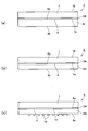
- (A) shows the state which provided the joining layer 2 on the support substrate 1 which consists of ceramics
- (b) shows the state which planarized the surface 3a of the joining layer 3
- (c) is a flat surface.
- 4 shows a state where 4 is activated by the neutralizing beam A.
- (A) shows a state where the piezoelectric single crystal substrate 6 and the support substrate 1 are joined
- (b) shows a state where the piezoelectric single crystal substrate 6A is thinned by processing
- (c) shows a state where the piezoelectric single crystal substrate 6A is thinned.
- a state in which the electrode 10 is provided on the crystal substrate 6A is shown.
- (A) shows a state in which the surface 11a of the piezoelectric single crystal substrate 11 is a rough surface
- (b) shows a state in which the intermediate layer 12 is provided on the rough surface 11a
- (c) shows a state in which the intermediate layer 12 is provided.
- 13 shows a state in which the surface 13a of 13 is flattened
- (d) shows a state in which the flat surface 14 is activated by the neutralizing beam A.
- (A) shows a state where the piezoelectric single crystal substrate 11 and the support substrate 1 are joined
- (b) shows a state where the piezoelectric single crystal substrate 11A is thinned by processing
- (c) shows a state where the piezoelectric single crystal substrate 11A is thinned.
- the state which provided the electrode 10 on 11 A of crystal substrates is shown.
- 1 and 2 relate to an embodiment in which a bonding layer is provided on a support substrate and this is directly bonded to the surface of a piezoelectric single crystal substrate.
- a bonding layer 2 is provided on a surface 1a of a support substrate 1 made of ceramics. 1b is the opposite surface. At this time, the surface 2a of the bonding layer 2 may be uneven.
- the flat surface 3 a is formed by flattening the surface 2 a of the bonding layer 2.
- the thickness of the bonding layer 2 is usually reduced, resulting in a thinner bonding layer 3 (see FIG. 1B).
- planarization is not always necessary.
- the flat surface 3 a is irradiated with a neutral beam as indicated by an arrow A to activate the surface of the bonding layer 3 ⁇ / b> A to be an activated surface 4.
- the surface of the piezoelectric single crystal substrate 6 is activated by irradiating it with a neutralized beam to obtain an activated surface 6a.
- the bonded body 7 is obtained by directly bonding the activation surface 6a of the piezoelectric single crystal substrate 6 and the activation surface 4 of the bonding layer 3A.
- the surface 6b of the piezoelectric single crystal substrate of the bonded body 7 is further polished to reduce the thickness of the piezoelectric single crystal substrate 6A as shown in FIG. Get. 6c is a polished surface.
- the surface acoustic wave element 9 is produced by forming a predetermined electrode 10 on the polished surface 6c of the piezoelectric single crystal substrate 6A.
- FIGS. 3 and 4 relate to an embodiment in which the surface of the piezoelectric single crystal substrate is rough.
- the surface 11a of the piezoelectric single crystal substrate 11 is processed to form a rough surface 11a.
- 11b is the opposite surface.
- the intermediate layer 12 is provided on the rough surface 11a.
- the rough surface is also transferred to the surface 12a of the intermediate layer 12, and irregularities are formed.
- the surface 12a of the intermediate layer 12 is flattened to form a flat surface 13a as shown in FIG.
- the thickness of the intermediate layer 12 is usually reduced, resulting in a thinner intermediate layer 13.
- the flat surface 13 a is irradiated with a neutral beam as indicated by an arrow A to activate the surface of the intermediate layer 13 ⁇ / b> A to be an activated surface 14.
- the flat surface of the bonding layer 3 ⁇ / b> A on the support substrate 1 is activated by irradiating with a neutral beam, thereby forming an activated surface 4.
- the joined surface 17 is obtained by directly joining the activated surface 4 of the joining layer 3A and the activated surface 14 of the intermediate layer 13A (FIG. 4A).
- the surface 11b of the piezoelectric single crystal substrate of the bonded body 17 is further polished to reduce the thickness of the piezoelectric material substrate 11A as shown in FIG. obtain.
- 11c is a polished surface.
- a predetermined electrode 10 is formed on the polishing surface 11c of the piezoelectric material substrate 11A.
- the support substrate is made of ceramics.
- a material selected from the group consisting of mullite, cordierite and sialon is preferable.
- a bonding layer is provided on the surface of the support substrate.
- the material of the bonding layer is one or more materials selected from the group consisting of mullite, alumina, tantalum pentoxide, titanium oxide and niobium pentoxide, thereby increasing the bonding strength between the bonding layer and the piezoelectric single crystal substrate. it can.
- the method for forming the bonding layer is not limited, and examples thereof include a sputtering method, a chemical vapor deposition method (CVD), and vapor deposition.
- the material of the piezoelectric single crystal substrate include lithium tantalate (LT) single crystal, lithium niobate (LN) single crystal, lithium niobate-lithium tantalate solid solution single crystal, crystal, and lithium borate. It can. Of these, LT or LN is more preferable. LT and LN are suitable as surface acoustic wave devices for high frequencies and wideband frequencies because of the high propagation speed of surface acoustic waves and a large electromechanical coupling coefficient.
- the normal direction of the principal surface of the piezoelectric single crystal substrate is not particularly limited.
- the piezoelectric single crystal substrate is made of LT
- the Y axis is centered on the X axis that is the propagation direction of the surface acoustic wave. It is preferable to use a direction rotated by 36 to 47 ° (for example, 42 °) from the Z axis to the small propagation loss.
- the piezoelectric material substrate is made of LN
- the size of the piezoelectric single crystal substrate is not particularly limited.
- the piezoelectric single crystal substrate has a diameter of 50 to 150 mm and a thickness of 0.2 to 60 ⁇ m.
- the arithmetic average roughness Ra of the surface of the support substrate is 0.5 nm or more and 5.0 nm or less. Thereby, peeling along the interface between the support substrate and the bonding layer can be remarkably suppressed. From this viewpoint, the arithmetic average roughness Ra of the surface of the support substrate is more preferably 0.8 nm or more, and further preferably 3.0 nm or less.
- the arithmetic average roughness Ra is a numerical value measured according to a measurement range of 10 ⁇ m ⁇ 10 ⁇ m using an AFM (Atomic Force Microscope).
- the PV value of the surface of the support substrate is 10 nm or more and 50 nm or less. This further improves the adhesion strength at the interface between the support substrate and the bonding layer. From this viewpoint, the PV value on the surface of the support substrate is more preferably 20 nm or more, and further preferably 30 nm or less.
- the PV value is a numerical value measured according to a measurement range of 10 ⁇ m ⁇ 10 ⁇ m using an AFM (Atomic Force Microscope).
- the surface of the bonding layer and the surface of the piezoelectric single crystal substrate are directly bonded.
- the arithmetic average roughness Ra of the surface of the bonding layer is preferably 1 nm or less, and more preferably 0.3 nm or less.
- the arithmetic average roughness Ra of the surface of the piezoelectric single crystal substrate is preferably 1 nm or less, and more preferably 0.3 nm or less. This further improves the bonding strength between the piezoelectric single crystal substrate and the bonding layer.
- an intermediate layer is provided between the piezoelectric single crystal substrate and the bonding layer, and the intermediate layer is selected from the group consisting of mullite, alumina, tantalum pentoxide, titanium oxide, and niobium pentoxide.
- the surface of the joining layer and the surface of the intermediate layer are joined. In this case, it is preferable to directly bond the surface of the piezoelectric single crystal substrate and the intermediate layer.
- the surface of the piezoelectric single crystal substrate is a surface on which periodic irregularities are uniformly formed in the plane, and the arithmetic average roughness Ra is 0.05 ⁇ m or more and 0.5 ⁇ m or less. is there. Thereby, spurious due to reflection at the interface of the bulk wave can be suppressed.
- the height Ry from the lowest valley bottom to the highest mountain peak on the surface of the piezoelectric single crystal substrate is 0.5 ⁇ m or more and 5.0 ⁇ m or less.
- the specific roughness depends on the wavelength of the elastic wave and can be appropriately selected so that reflection of the bulk wave can be suppressed.
- the roughening method includes grinding, polishing, etching, sand blasting, and the like.
- the intermediate layer is made of one or more materials selected from the group consisting of mullite, alumina, tantalum pentoxide, titanium oxide and niobium pentoxide.
- the method for forming the intermediate layer is not limited, and examples thereof include sputtering, chemical vapor deposition (CVD), and vapor deposition.
- the arithmetic average roughness Ra of the surface of the intermediate layer is preferably 1 nm or less, and more preferably 0.3 nm or less.
- Methods for flattening the surface of the intermediate layer include lap polishing and chemical mechanical polishing (CMP).
- the surface of the piezoelectric single crystal substrate can be activated by a neutralizing beam.
- the surface of the piezoelectric single crystal substrate is a flat surface
- the surface can be directly bonded to the bonding layer.
- the flat surface of the bonding layer is activated by irradiating the flat surface of the bonding layer with a neutral beam.
- a saddle field type fast atomic beam source is used as the beam source.
- an inert gas is introduced into the chamber, and a high voltage is applied to the electrodes from a DC power source.
- the saddle field type electric field generated between the electrode (positive electrode) and the casing (negative electrode) moves the electrons e, thereby generating atomic and ion beams by the inert gas.
- the ion beam is neutralized by the grid, so that a beam of neutral atoms is emitted from the fast atom beam source.
- the atomic species constituting the beam is preferably an inert gas (argon, nitrogen, etc.).
- the voltage upon activation by beam irradiation is preferably 0.5 to 2.0 kV, and the current is preferably 50 to 200 mA.
- the temperature at this time is room temperature, but specifically, it is preferably 40 ° C. or lower, more preferably 30 ° C. or lower.
- the temperature at the time of joining is particularly preferably 20 ° C. or higher and 25 ° C. or lower.
- the pressure at the time of joining is preferably 100 to 20000 N.
- acoustic wave element or an optical element.
- acoustic wave elements include surface acoustic wave devices, Lamb wave elements, thin film resonators (FBARs), and the like.
- FBARs thin film resonators
- a surface acoustic wave device has an IDT (Interdigital Transducer) electrode (also referred to as a comb-shaped electrode or a comb-shaped electrode) for exciting surface acoustic waves on the surface of a piezoelectric material substrate and an output side for receiving surface acoustic waves. IDT electrodes are provided.
- IDT Interdigital Transducer
- a metal film may be provided on the bottom surface of the piezoelectric single crystal substrate.
- the metal film plays a role of increasing the electromechanical coupling coefficient in the vicinity of the back surface of the piezoelectric substrate when a Lamb wave element is manufactured as an elastic wave device.
- the Lamb wave element has a structure in which comb electrodes are formed on the surface of the piezoelectric single crystal substrate, and the metal film of the piezoelectric substrate is exposed by the cavity provided in the support substrate.
- Examples of the material of such a metal film include aluminum, an aluminum alloy, copper, and gold.
- a metal film and an insulating film may be provided on the bottom surface of the piezoelectric single crystal substrate.
- the metal film serves as an electrode when a thin film resonator is manufactured as an acoustic wave device.
- the thin film resonator has a structure in which electrodes are formed on the front and back surfaces of the piezoelectric substrate, and the metal film of the piezoelectric substrate is exposed by using the insulating film as a cavity.
- the material for such a metal film include molybdenum, ruthenium, tungsten, chromium, and aluminum.
- the material for the insulating film include silicon dioxide, phosphorous silica glass, and boron phosphorous silica glass.
- examples of the optical element include an optical switching element, a wavelength conversion element, and an optical modulation element.
- a periodically poled structure can be formed in the piezoelectric material substrate.
- the present invention When the present invention is applied to an optical element, it is possible to reduce the size of the optical element. In particular, when a periodic polarization reversal structure is formed, deterioration of the periodic polarization reversal structure due to heat treatment can be prevented. Furthermore, since the bonding layer material of the present invention is also a highly insulating material, the occurrence of polarization reversal is suppressed during the treatment with the neutralized beam before bonding, and the periodically poled structure formed on the piezoelectric single crystal substrate There is almost no disturbing shape.
- Example A1 A joined body was produced according to the method described with reference to FIGS. Specifically, a lithium tantalate substrate (LT substrate) having an orientation flat portion (OF portion), a diameter of 4 inches, and a thickness of 250 ⁇ m was used as the piezoelectric single crystal substrate 6.
- LT substrate a lithium tantalate substrate having an orientation flat portion (OF portion), a diameter of 4 inches, and a thickness of 250 ⁇ m was used as the piezoelectric single crystal substrate 6.
- LT substrate a 46 ° Y-cut X-propagation LT substrate in which the propagation direction of the surface acoustic wave (SAW) is X and the cutting angle is a rotating Y-cut plate is used.
- the surface 6a of the piezoelectric single crystal substrate 6 was mirror-polished so that the arithmetic average roughness Ra was 0.3 nm.
- a mullite substrate having an OF portion, a diameter of 4 inches, and a thickness of 230 ⁇ m was prepared as the support substrate 1.
- the arithmetic average roughness Ra of the surface 1a of the support substrate 1 made of mullite is 0.5 nm, and the PV value is 10 nm.
- Arithmetic mean roughness was evaluated by an atomic force microscope (AFM) with a square field of 10 ⁇ m length ⁇ 10 ⁇ m width.
- a bonding layer 2 made of mullite was formed on the surface 1 a of the support substrate 1 by a CVD method with a thickness of 1.0 ⁇ m. Ra after film formation was 2.0 nm.
- the bonding layer 2 was subjected to chemical mechanical polishing (CMP), the film thickness was set to 0.1 ⁇ m, and Ra was set to 0.3 nm.
- CMP chemical mechanical polishing
- the flat surface 3a of the bonding layer 3 and the surface 6a of the piezoelectric single crystal substrate 6 were cleaned, removed, and then introduced into a vacuum chamber. After evacuation to a level of 10 ⁇ 6 Pa, high-speed atomic beams (acceleration voltage 1 kV, Ar flow rate 27 sccm) were irradiated for 120 seconds to the bonding surfaces of the respective substrates. Next, after the beam irradiation surface (activation surface) 4 of the bonding layer 3A and the activation surface 6a of the piezoelectric single crystal substrate 6 were brought into contact with each other, the substrates were bonded by pressing at 10000 N for 2 minutes.
- the surface 6b of the piezoelectric single crystal substrate 6 was ground and polished so that the thickness was changed from the initial 250 ⁇ m to 20 ⁇ m (see FIG. 2B). During the grinding and polishing process, no peeling of the joint could be confirmed. Moreover, when the joint strength was evaluated by a crack opening method, it was 1.4 J / m 2 .
- the tape peeling test was performed as follows. A 2 ⁇ 2 mm square slit is formed on the wafer. The slit has a depth that penetrates the piezoelectric single crystal and enters part of the support substrate. A test tape is applied to the piezoelectric single crystal substrate. As the test tape, an adhesive tape defined in JIS Z 1522 was used. After pressing for 5 seconds with a finger, the tape was pulled strongly to be perpendicular to the substrate and peeled off.
- Example 1 (Examples A2 to A4 and Comparative Examples A1 to A4)
- Example 2 by changing the grindstone used for processing the surface of the support substrate, the Ra and PV values of the surface of the support substrate were changed as shown in Table 1, and bonding of Examples A2 to A4 and Comparative Examples A1 to A4 was performed. Got the body.
- Comparative Example A4 the thickness of the bonding layer was changed to 300 nm.
- Example B In Examples A1 to A4 and Comparative Examples A1 to A3, the bonding layer 2 was made of alumina, and the bonding layer 2 was formed by sputtering. Others were manufactured in the same manner as in Example A1.
- Example C In Examples A1 to A4 and Comparative Examples A1 to A3, the material of the bonding layer 2 was tantalum pentoxide, and the bonding layer 2 was formed by sputtering. Others were manufactured in the same manner as in Example A1.
- Example D In Examples A1 to A4 and Comparative Examples A1 to A3, the bonding layer 2 was made of titanium oxide, and the bonding layer 2 was formed by sputtering. Others were manufactured in the same manner as in Example A1.
- Example E In Examples A1 to A4 and Comparative Examples A1 to A3, the bonding layer 2 was made of niobium pentoxide, and the bonding layer 2 was formed by sputtering. Others were manufactured in the same manner as in Example A1.
- Example F1 Comparative Example F1
- the material of the bonding layer 2 was silicon nitride, and the sputtering method was used to form the bonding layer 2. Otherwise, the joined body was manufactured in the same manner as in Example A1. As a result, peeling of the joint portion occurred during the grinding and polishing process of the piezoelectric single crystal substrate. Moreover, it was 0.6 J / m ⁇ 2 > when the joining strength was evaluated by the crack opening method.
- Example F2 Comparative Example F2
- the material of the bonding layer 2 was aluminum nitride, and the sputtering method was used to form the bonding layer 2. Otherwise, the joined body was manufactured in the same manner as in Example A1. As a result, peeling of the joint portion occurred during the grinding and polishing process of the piezoelectric single crystal substrate. Moreover, when the joint strength was evaluated by a crack opening method, it was 0.5 J / m 2 .
- Example F3 In Example A1, the material of the bonding layer 2 was silicon oxide, and the sputtering method was used to form the bonding layer 2. Otherwise, the joined body was manufactured in the same manner as in Example A1. As a result, peeling of the joint portion occurred during the grinding and polishing process of the piezoelectric single crystal substrate. Moreover, it was 0.1 J / m ⁇ 2 > when the joining strength was evaluated by the crack opening method.
Landscapes
- Physics & Mathematics (AREA)
- Acoustics & Sound (AREA)
- Engineering & Computer Science (AREA)
- Manufacturing & Machinery (AREA)
- Chemical & Material Sciences (AREA)
- Ceramic Engineering (AREA)
- Materials Engineering (AREA)
- Surface Acoustic Wave Elements And Circuit Networks Thereof (AREA)
Abstract
Description
例えば、特許文献1には、圧電基板とシリコン基板とをエポキシ接着剤からなる接着層によって貼り合わせた構造の弾性表面波デバイスが提案されている。
セラミックスからなる支持基板、
前記支持基板の表面に設けられた接合層であって、ムライト、アルミナ、五酸化タンタル、酸化チタンおよび五酸化ニオブからなる群より選ばれた一種以上の材質からなる接合層、および
前記接合層に接合された圧電性単結晶基板
を有しており、前記支持基板の前記表面の算術平均粗さRaが0.5nm以上、5.0nm以下であることを特徴とする。
前記接合体、および
前記圧電性単結晶基板上に設けられた電極を備えていることを特徴とする。
図1、図2は、支持基板上に接合層を設け、これを圧電性単結晶基板の表面に直接接合する実施形態に係るものである。
次いで、図1(c)に示すように、平坦面3aに対して矢印Aのように中性化ビームを照射し、接合層3Aの表面を活性化して活性化面4とする。
支持基板はセラミックスからなる。支持基板を構成するセラミックスとしては、ムライト、コージェライトおよびサイアロンからなる群より選ばれた材質が好ましい。
また、粗面化加工の方法は、研削、研磨、エッチング、サンドブラストなどがある。
ビーム照射による活性化時の電圧は0.5~2.0kVとすることが好ましく、電流は50~200mAとすることが好ましい。
弾性波素子としては、弾性表面波デバイスやラム波素子、薄膜共振子(FBAR)などが知られている。例えば、弾性表面波デバイスは、圧電性材料基板の表面に、弾性表面波を励振する入力側のIDT(Interdigital Transducer)電極(櫛形電極、すだれ状電極ともいう)と弾性表面波を受信する出力側のIDT電極とを設けたものである。入力側のIDT電極に高周波信号を印加すると、電極間に電界が発生し、弾性表面波が励振されて圧電基板上を伝搬していく。そして、伝搬方向に設けられた出力側のIDT電極から、伝搬された弾性表面波を電気信号として取り出すことができる。
図1~図2を参照しつつ説明した方法に従って、接合体を作製した。
具体的には、オリエンテーションフラット部(OF部)を有し、直径が4インチ,厚さが250μmのタンタル酸リチウム基板(LT基板)を、圧電性単結晶基板6として使用した。LT基板は、弾性表面波(SAW)の伝搬方向をXとし、切り出し角が回転Yカット板である46°YカットX伝搬LT基板を用いた。圧電性単結晶基板6の表面6aは、算術平均粗さRaが0.3nmとなるように鏡面研磨しておいた。
ウェハーに2×2mmの正方形のスリットを形成する。スリットは、圧電単結晶を貫通し、支持基板の途中まで入り込むような深さにした。試験用テープを圧電単結晶基板に貼り付ける。試験用テープは、JIS Z 1522に規定された粘着テープを使用した。指で5秒間押したあと、テープを基板に垂直になるように強く引っ張り、引き剥がした。
実施例1において、支持基板表面の加工に用いる砥石を変更することで、支持基板表面のRaおよびPV値を表1に示すように変更し、実施例A2~A4および比較例A1~A4の接合体を得た。ただし、比較例A4においては、接合層の厚さを300nmに変更した。

実施例A1~A4、比較例A1~A3において、接合層2の材質をアルミナとし、接合層2の成膜にはスパッタリング法を用いた。その他は実施例A1と同様にして各接合体を製造した。
実施例A1~A4、比較例A1~A3において、接合層2の材質を五酸化タンタルとし、接合層2の成膜にはスパッタリング法を用いた。その他は実施例A1と同様にして各接合体を製造した。
実施例A1~A4、比較例A1~A3において、接合層2の材質を酸化チタンとし、接合層2の成膜にはスパッタリング法を用いた。その他は実施例A1と同様にして各接合体を製造した。
実施例A1~A4、比較例A1~A3において、接合層2の材質を五酸化ニオブとし、接合層2の成膜にはスパッタリング法を用いた。その他は実施例A1と同様にして各接合体を製造した。
実施例A1において、接合層2の材質を窒化珪素とし、接合層2の成膜にはスパッタリング法を用いた。その他は実施例A1と同様にして接合体を製造した。
この結果、圧電性単結晶基板の研削および研磨工程中に接合部分の剥がれが発生した。またクラックオープニング法で接合強度を評価した所、0.6J/m2であった。
実施例A1において、接合層2の材質を窒化アルミニウムとし、接合層2の成膜にはスパッタリング法を用いた。その他は実施例A1と同様にして接合体を製造した。
この結果、圧電性単結晶基板の研削および研磨工程中に接合部分の剥がれが発生した。またクラックオープニング法で接合強度を評価した所、0.5J/m2であった。
実施例A1において、接合層2の材質を酸化珪素とし、接合層2の成膜にはスパッタリング法を用いた。その他は実施例A1と同様にして接合体を製造した。
この結果、圧電性単結晶基板の研削および研磨工程中に接合部分の剥がれが発生した。またクラックオープニング法で接合強度を評価した所、0.1J/m2であった。
Claims (9)
- セラミックスからなる支持基板、
前記支持基板の表面に設けられた接合層であって、ムライト、アルミナ、五酸化タンタル、酸化チタンおよび五酸化ニオブからなる群より選ばれた一種以上の材質からなる接合層、および
前記接合層に接合された圧電性単結晶基板
を有しており、前記支持基板の前記表面の算術平均粗さRaが0.5nm以上、5.0nm以下であることを特徴とする、接合体。 - 前記支持基板が、ムライト、コージェライトおよびサイアロンからなる群より選ばれた材質からなることを特徴とする、請求項1記載の接合体。
- 前記接合層の表面と前記圧電性単結晶基板の表面とが直接接合されていることを特徴とする、請求項1または2記載の接合体。
- 前記接合層の前記表面の算術平均粗さRaが1nm以下であり、前記圧電性単結晶基板の前記表面の算術平均粗さRaが1nm以下であることを特徴とする、請求項3記載の接合体。
- 前記圧電性単結晶基板と前記接合層との間に中間層を有しており、前記中間層がムライト、アルミナ、五酸化タンタル、酸化チタンおよび五酸化ニオブからなる群より選ばれた一種以上の材質からなり、前記接合層の表面と前記中間層の表面とが接合されていることを特徴とする、請求項1または2記載の接合体。
- 前記圧電性単結晶基板の表面上に前記中間層が設けられており、前記圧電性単結晶基板の前記表面の算術平均粗さRaが0.05μm以上、0.5μm以下であることを特徴とする、請求項5記載の接合体。
- 前記接合層の前記表面の算術平均粗さRaが1nm以下であり、前記中間層の前記表面の算術平均粗さRaが1nm以下であることを特徴とする、請求項5または6記載の接合体。
- 前記圧電性単結晶基板が、ニオブ酸リチウム、タンタル酸リチウムまたはニオブ酸リチウム-タンタル酸リチウム固溶体からなることを特徴とする、請求項1~7のいずれか一つの請求項に記載の接合体。
- 請求項1~8のいずれか一つの請求項に記載の接合体、および前記圧電性単結晶基板上に設けられた電極を備えていることを特徴とする、弾性波素子。
Priority Applications (6)
| Application Number | Priority Date | Filing Date | Title |
|---|---|---|---|
| KR1020197034939A KR20190134827A (ko) | 2016-03-25 | 2017-02-22 | 접합체 및 탄성파 소자 |
| DE112017001553.7T DE112017001553B4 (de) | 2016-03-25 | 2017-02-22 | Verbundener Körper und Elastikwellenelement |
| KR1020187022885A KR102183134B1 (ko) | 2016-03-25 | 2017-02-22 | 접합체 및 탄성파 소자 |
| CN201780013563.6A CN109075758B (zh) | 2016-03-25 | 2017-02-22 | 接合体和弹性波元件 |
| JP2018507148A JP6427714B2 (ja) | 2016-03-25 | 2017-02-22 | 接合体および弾性波素子 |
| US16/135,655 US10432169B2 (en) | 2016-03-25 | 2018-09-19 | Bonded body and elastic wave element |
Applications Claiming Priority (2)
| Application Number | Priority Date | Filing Date | Title |
|---|---|---|---|
| JP2016-061713 | 2016-03-25 | ||
| JP2016061713 | 2016-03-25 |
Related Child Applications (1)
| Application Number | Title | Priority Date | Filing Date |
|---|---|---|---|
| US16/135,655 Continuation US10432169B2 (en) | 2016-03-25 | 2018-09-19 | Bonded body and elastic wave element |
Publications (1)
| Publication Number | Publication Date |
|---|---|
| WO2017163729A1 true WO2017163729A1 (ja) | 2017-09-28 |
Family
ID=59899977
Family Applications (2)
| Application Number | Title | Priority Date | Filing Date |
|---|---|---|---|
| PCT/JP2017/006476 Ceased WO2017163729A1 (ja) | 2016-03-25 | 2017-02-22 | 接合体および弾性波素子 |
| PCT/JP2017/006463 Ceased WO2017163723A1 (ja) | 2016-03-25 | 2017-02-22 | 接合方法 |
Family Applications After (1)
| Application Number | Title | Priority Date | Filing Date |
|---|---|---|---|
| PCT/JP2017/006463 Ceased WO2017163723A1 (ja) | 2016-03-25 | 2017-02-22 | 接合方法 |
Country Status (7)
| Country | Link |
|---|---|
| US (2) | US10432169B2 (ja) |
| JP (2) | JP6427713B2 (ja) |
| KR (4) | KR20190134827A (ja) |
| CN (2) | CN109075758B (ja) |
| DE (2) | DE112017001539B4 (ja) |
| TW (2) | TWI672839B (ja) |
| WO (2) | WO2017163729A1 (ja) |
Cited By (8)
| Publication number | Priority date | Publication date | Assignee | Title |
|---|---|---|---|---|
| WO2019130852A1 (ja) * | 2017-12-28 | 2019-07-04 | 日本碍子株式会社 | 圧電性材料基板と支持基板との接合体およびその製造方法 |
| WO2019130857A1 (ja) * | 2017-12-28 | 2019-07-04 | 日本碍子株式会社 | 圧電性材料基板と支持基板との接合体およびその製造方法 |
| JP2020091144A (ja) * | 2018-12-04 | 2020-06-11 | 浜松ホトニクス株式会社 | シンチレータモジュール、放射線撮像装置、及びシンチレータモジュールの製造方法 |
| JP2021517384A (ja) * | 2018-03-30 | 2021-07-15 | ソイテックSoitec | 表面弾性波デバイス用のハイブリッド構造及び関連する製造方法 |
| WO2022054372A1 (ja) * | 2020-09-10 | 2022-03-17 | 日本碍子株式会社 | 弾性波デバイス用複合基板 |
| WO2022071605A1 (ja) * | 2020-10-02 | 2022-04-07 | 株式会社村田製作所 | 弾性波装置及び弾性波装置の製造方法 |
| WO2022158249A1 (ja) * | 2021-01-19 | 2022-07-28 | 株式会社村田製作所 | 弾性波装置、フィルタ装置及び弾性波装置の製造方法 |
| JP2023083605A (ja) * | 2020-04-02 | 2023-06-15 | 信越化学工業株式会社 | 複合基板およびその製造方法 |
Families Citing this family (25)
| Publication number | Priority date | Publication date | Assignee | Title |
|---|---|---|---|---|
| US20180241374A1 (en) * | 2015-09-25 | 2018-08-23 | Avago Technologies General Ip (Singapore) Pte. Ltd | Acoustic wave resonator having antiresonant cavity |
| US20180337657A1 (en) * | 2015-09-25 | 2018-11-22 | Avago Technologies General Ip (Singapore) Pte. Ltd. | Acoustic wave resonator having antiresonant cavity |
| KR20190134827A (ko) * | 2016-03-25 | 2019-12-04 | 엔지케이 인슐레이터 엘티디 | 접합체 및 탄성파 소자 |
| WO2017163722A1 (ja) * | 2016-03-25 | 2017-09-28 | 日本碍子株式会社 | 接合方法 |
| TWI737811B (zh) | 2016-11-25 | 2021-09-01 | 日商日本碍子股份有限公司 | 接合體 |
| TWI780103B (zh) * | 2017-05-02 | 2022-10-11 | 日商日本碍子股份有限公司 | 彈性波元件及其製造方法 |
| DE112018000207B4 (de) * | 2017-09-15 | 2024-02-22 | Ngk Insulators, Ltd. | Akustikwellenvorrichtung und ein Verfahren zu deren Herstellung |
| WO2019142483A1 (ja) | 2018-01-22 | 2019-07-25 | 日本碍子株式会社 | 圧電性材料基板と支持基板との接合体およびその製造方法 |
| CN112088439B (zh) * | 2018-05-16 | 2022-04-22 | 日本碍子株式会社 | 压电性材料基板与支撑基板的接合体 |
| CN110858763B (zh) * | 2018-08-22 | 2025-07-08 | 天工方案公司 | 多层压电基板 |
| KR102596121B1 (ko) * | 2018-10-17 | 2023-10-30 | 엔지케이 인슐레이터 엘티디 | 접합체 및 탄성파 소자 |
| JP7069338B2 (ja) * | 2018-10-17 | 2022-05-17 | 日本碍子株式会社 | 接合体および弾性波素子 |
| CN109855592B (zh) * | 2019-01-08 | 2020-07-28 | 湘潭大学 | 基体结合面粗糙度确定方法及装置、复合材料加工方法 |
| KR102729394B1 (ko) * | 2019-06-11 | 2024-11-13 | 엔지케이 인슐레이터 엘티디 | 복합 기판, 탄성파 소자 및 복합 기판의 제조 방법 |
| EP3985870B1 (en) * | 2019-06-11 | 2025-11-05 | NGK Insulators, Ltd. | Composite substrate, elastic wave element, and production method for composite substrate |
| WO2021002382A1 (ja) | 2019-07-01 | 2021-01-07 | 株式会社村田製作所 | 弾性波装置 |
| US11183987B2 (en) * | 2019-09-26 | 2021-11-23 | Avago Technologies International Sales Pte. Limited | Acoustic resonator device |
| KR102402925B1 (ko) * | 2019-11-29 | 2022-05-30 | 엔지케이 인슐레이터 엘티디 | 압전성 재료 기판과 지지 기판의 접합체 |
| CN114731150B (zh) * | 2019-11-29 | 2025-09-30 | 日本碍子株式会社 | 压电性材料基板与支撑基板的接合体 |
| JP7384277B2 (ja) * | 2020-04-22 | 2023-11-21 | 株式会社村田製作所 | 圧電デバイス |
| CN112320897B (zh) * | 2020-10-09 | 2022-07-22 | 新昌中国计量大学企业创新研究院有限公司 | 一种球状铁碳微电解填料及其制备方法 |
| KR102539925B1 (ko) * | 2021-03-10 | 2023-06-02 | 엔지케이 인슐레이터 엘티디 | 접합체 |
| ES2936907B2 (es) | 2021-09-14 | 2023-08-11 | Quim Tecnica Ecologica S L U | Metodo y equipos para la produccion de polihidroxialcanoatos y bioestimulante radicular a partir de residuos organicos |
| KR102741639B1 (ko) * | 2021-11-19 | 2024-12-16 | (주)위드멤스 | 기판 접합체 및 기판 접합 방법 |
| KR102728250B1 (ko) | 2022-10-11 | 2024-11-11 | (재)한국나노기술원 | 이종 기판의 접합 구조체 및 그 제조방법 그리고 이를 이용한 탄성파 소자 |
Citations (4)
| Publication number | Priority date | Publication date | Assignee | Title |
|---|---|---|---|---|
| WO2013146374A1 (ja) * | 2012-03-26 | 2013-10-03 | 株式会社村田製作所 | 弾性波装置及びその製造方法 |
| WO2014010696A1 (ja) * | 2012-07-12 | 2014-01-16 | 日本碍子株式会社 | 複合基板、圧電デバイス及び複合基板の製法 |
| WO2014192597A1 (ja) * | 2013-05-31 | 2014-12-04 | 日本碍子株式会社 | 複合基板用支持基板および複合基板 |
| JP2015145054A (ja) * | 2014-02-04 | 2015-08-13 | 日本碍子株式会社 | 複合基板の研磨方法及び複合基板 |
Family Cites Families (32)
| Publication number | Priority date | Publication date | Assignee | Title |
|---|---|---|---|---|
| JPS5814727B2 (ja) | 1974-09-25 | 1983-03-22 | 富士写真フイルム株式会社 | キヨウジセイサンカテツノ セイホウ |
| JPS5814727A (ja) | 1981-07-17 | 1983-01-27 | Polyurethan Eng:Kk | 板状品の連続成形機におけるコンベア駆動方法 |
| JPH027480A (ja) * | 1988-06-24 | 1990-01-11 | Nissha Printing Co Ltd | 圧電磁器の製造方法 |
| JP3814763B2 (ja) | 1995-03-31 | 2006-08-30 | 東レフィルム加工株式会社 | コーティングフィルムの製造方法 |
| JP3465675B2 (ja) * | 2000-09-11 | 2003-11-10 | 日本碍子株式会社 | 圧電/電歪膜型素子 |
| JP3512379B2 (ja) * | 2000-09-20 | 2004-03-29 | 日本碍子株式会社 | 圧電体素子、及びその製造方法 |
| US7105980B2 (en) | 2002-07-03 | 2006-09-12 | Sawtek, Inc. | Saw filter device and method employing normal temperature bonding for producing desirable filter production and performance characteristics |
| JP3774782B2 (ja) | 2003-05-14 | 2006-05-17 | 富士通メディアデバイス株式会社 | 弾性表面波素子の製造方法 |
| JP2005045086A (ja) * | 2003-07-24 | 2005-02-17 | Nec Tokin Corp | インジェクタ装置用積層型圧電素子 |
| JP2005349714A (ja) * | 2004-06-11 | 2005-12-22 | Canon Inc | 液体吐出ヘッドの製造方法および液体吐出ヘッド |
| US7538401B2 (en) * | 2005-05-03 | 2009-05-26 | Rosemount Aerospace Inc. | Transducer for use in harsh environments |
| FR2896618B1 (fr) * | 2006-01-23 | 2008-05-23 | Soitec Silicon On Insulator | Procede de fabrication d'un substrat composite |
| JP5288719B2 (ja) * | 2007-03-27 | 2013-09-11 | 京セラ株式会社 | 液体吐出ヘッド用積層圧電アクチュエータおよびその製造方法ならびに液体吐出ヘッド |
| JP4720808B2 (ja) | 2007-09-21 | 2011-07-13 | セイコーエプソン株式会社 | 接着シート、接合方法および接合体 |
| JP4442671B2 (ja) * | 2007-09-21 | 2010-03-31 | セイコーエプソン株式会社 | 接合膜付き基材、接合方法および接合体 |
| JP4348454B2 (ja) | 2007-11-08 | 2009-10-21 | 三菱重工業株式会社 | デバイスおよびデバイス製造方法 |
| JP2010187373A (ja) | 2009-01-19 | 2010-08-26 | Ngk Insulators Ltd | 複合基板及びそれを用いた弾性波デバイス |
| KR101374303B1 (ko) * | 2009-11-26 | 2014-03-14 | 가부시키가이샤 무라타 세이사쿠쇼 | 압전 디바이스 및 압전 디바이스의 제조방법 |
| JP5669443B2 (ja) * | 2010-05-31 | 2015-02-12 | キヤノン株式会社 | 振動体とその製造方法及び振動波アクチュエータ |
| CN203014754U (zh) | 2010-06-15 | 2013-06-19 | 日本碍子株式会社 | 复合基板 |
| CN102624352B (zh) * | 2010-10-06 | 2015-12-09 | 日本碍子株式会社 | 复合基板的制造方法以及复合基板 |
| JP2013214954A (ja) * | 2012-03-07 | 2013-10-17 | Taiyo Yuden Co Ltd | 共振子、周波数フィルタ、デュプレクサ、電子機器及び共振子の製造方法 |
| KR101443015B1 (ko) | 2012-08-17 | 2014-09-22 | 엔지케이 인슐레이터 엘티디 | 복합 기판, 탄성 표면파 디바이스 및 복합 기판의 제조방법 |
| JP2014086400A (ja) * | 2012-10-26 | 2014-05-12 | Mitsubishi Heavy Ind Ltd | 高速原子ビーム源およびそれを用いた常温接合装置 |
| CN105164919B (zh) * | 2013-03-21 | 2017-04-26 | 日本碍子株式会社 | 弹性波元件用复合基板及弹性波元件 |
| US10541667B2 (en) * | 2015-08-25 | 2020-01-21 | Avago Technologies International Sales Pte. Limited | Surface acoustic wave (SAW) resonator having trap-rich region |
| US10530327B2 (en) * | 2015-08-25 | 2020-01-07 | Avago Technologies International Sales Pte. Limited | Surface acoustic wave (SAW) resonator |
| US10177734B2 (en) * | 2015-08-25 | 2019-01-08 | Avago Technologies International Sales Pte. Limited | Surface acoustic wave (SAW) resonator |
| WO2017068828A1 (ja) * | 2015-10-23 | 2017-04-27 | 株式会社村田製作所 | 弾性波装置 |
| KR20190134827A (ko) * | 2016-03-25 | 2019-12-04 | 엔지케이 인슐레이터 엘티디 | 접합체 및 탄성파 소자 |
| WO2017163722A1 (ja) * | 2016-03-25 | 2017-09-28 | 日本碍子株式会社 | 接合方法 |
| WO2018180827A1 (ja) * | 2017-03-31 | 2018-10-04 | 日本碍子株式会社 | 接合体および弾性波素子 |
-
2017
- 2017-02-22 KR KR1020197034939A patent/KR20190134827A/ko not_active Withdrawn
- 2017-02-22 CN CN201780013563.6A patent/CN109075758B/zh active Active
- 2017-02-22 DE DE112017001539.1T patent/DE112017001539B4/de active Active
- 2017-02-22 WO PCT/JP2017/006476 patent/WO2017163729A1/ja not_active Ceased
- 2017-02-22 KR KR1020187022829A patent/KR102127260B1/ko active Active
- 2017-02-22 WO PCT/JP2017/006463 patent/WO2017163723A1/ja not_active Ceased
- 2017-02-22 TW TW106105857A patent/TWI672839B/zh active
- 2017-02-22 JP JP2018507142A patent/JP6427713B2/ja active Active
- 2017-02-22 CN CN201780017024.XA patent/CN108886347B/zh active Active
- 2017-02-22 JP JP2018507148A patent/JP6427714B2/ja active Active
- 2017-02-22 TW TW106105858A patent/TWI664754B/zh active
- 2017-02-22 DE DE112017001553.7T patent/DE112017001553B4/de active Active
- 2017-02-22 KR KR1020197034785A patent/KR20190133794A/ko not_active Withdrawn
- 2017-02-22 KR KR1020187022885A patent/KR102183134B1/ko active Active
-
2018
- 2018-09-19 US US16/135,655 patent/US10432169B2/en active Active
- 2018-09-19 US US16/135,577 patent/US10720566B2/en active Active
Patent Citations (4)
| Publication number | Priority date | Publication date | Assignee | Title |
|---|---|---|---|---|
| WO2013146374A1 (ja) * | 2012-03-26 | 2013-10-03 | 株式会社村田製作所 | 弾性波装置及びその製造方法 |
| WO2014010696A1 (ja) * | 2012-07-12 | 2014-01-16 | 日本碍子株式会社 | 複合基板、圧電デバイス及び複合基板の製法 |
| WO2014192597A1 (ja) * | 2013-05-31 | 2014-12-04 | 日本碍子株式会社 | 複合基板用支持基板および複合基板 |
| JP2015145054A (ja) * | 2014-02-04 | 2015-08-13 | 日本碍子株式会社 | 複合基板の研磨方法及び複合基板 |
Cited By (27)
| Publication number | Priority date | Publication date | Assignee | Title |
|---|---|---|---|---|
| US11700771B2 (en) | 2017-12-28 | 2023-07-11 | Ngk Insulators, Ltd. | Assembly of piezoelectric material substrate and support substrate, and method for manufacturing said assembly |
| CN111512549B (zh) * | 2017-12-28 | 2023-10-17 | 日本碍子株式会社 | 压电性材料基板与支撑基板的接合体及其制造方法 |
| JPWO2019130852A1 (ja) * | 2017-12-28 | 2019-12-26 | 日本碍子株式会社 | 圧電性材料基板と支持基板との接合体およびその製造方法 |
| JPWO2019130857A1 (ja) * | 2017-12-28 | 2019-12-26 | 日本碍子株式会社 | 圧電性材料基板と支持基板との接合体およびその製造方法 |
| KR20200033326A (ko) * | 2017-12-28 | 2020-03-27 | 엔지케이 인슐레이터 엘티디 | 압전성 재료 기판과 지지 기판의 접합체 및 그 제조 방법 |
| DE112018004250B4 (de) | 2017-12-28 | 2022-06-15 | Ngk Insulators, Ltd. | Anordnung eines Substrats aus einem piezoelektrischen Material und eines Trägersubstrats und Verfahren zur Herstellung der Anordnung |
| CN111492577A (zh) * | 2017-12-28 | 2020-08-04 | 日本碍子株式会社 | 压电性材料基板与支撑基板的接合体及其制造方法 |
| CN111512549A (zh) * | 2017-12-28 | 2020-08-07 | 日本碍子株式会社 | 压电性材料基板与支撑基板的接合体及其制造方法 |
| CN111492577B (zh) * | 2017-12-28 | 2024-04-02 | 日本碍子株式会社 | 压电性材料基板与支撑基板的接合体及其制造方法 |
| KR102341608B1 (ko) * | 2017-12-28 | 2021-12-22 | 엔지케이 인슐레이터 엘티디 | 압전성 재료 기판과 지지 기판의 접합체 및 그 제조 방법 |
| DE112018005782B4 (de) | 2017-12-28 | 2024-02-22 | Ngk Insulators, Ltd. | Anordnung eines Substrats aus einem piezoelektrischen Material und eines Trägersubstrats |
| WO2019130852A1 (ja) * | 2017-12-28 | 2019-07-04 | 日本碍子株式会社 | 圧電性材料基板と支持基板との接合体およびその製造方法 |
| WO2019130857A1 (ja) * | 2017-12-28 | 2019-07-04 | 日本碍子株式会社 | 圧電性材料基板と支持基板との接合体およびその製造方法 |
| US11689172B2 (en) | 2017-12-28 | 2023-06-27 | Ngk Insulators, Ltd. | Assembly of piezoelectric material substrate and support substrate, and method for manufacturing said assembly |
| JP2021517384A (ja) * | 2018-03-30 | 2021-07-15 | ソイテックSoitec | 表面弾性波デバイス用のハイブリッド構造及び関連する製造方法 |
| JP7480930B2 (ja) | 2018-03-30 | 2024-05-10 | ソイテック | 表面弾性波デバイス用のハイブリッド構造及び関連する製造方法 |
| US11974505B2 (en) | 2018-03-30 | 2024-04-30 | Soitec | Hybrid structure for surface acoustic wave device and associated production method |
| JP2020091144A (ja) * | 2018-12-04 | 2020-06-11 | 浜松ホトニクス株式会社 | シンチレータモジュール、放射線撮像装置、及びシンチレータモジュールの製造方法 |
| JP7515657B2 (ja) | 2020-04-02 | 2024-07-12 | 信越化学工業株式会社 | 複合基板およびその製造方法 |
| JP2023083605A (ja) * | 2020-04-02 | 2023-06-15 | 信越化学工業株式会社 | 複合基板およびその製造方法 |
| JP7625535B2 (ja) | 2020-09-10 | 2025-02-03 | 日本碍子株式会社 | 弾性波デバイス用複合基板 |
| JPWO2022054372A1 (ja) * | 2020-09-10 | 2022-03-17 | ||
| CN115956339A (zh) * | 2020-09-10 | 2023-04-11 | 日本碍子株式会社 | 弹性波器件用复合基板 |
| WO2022054372A1 (ja) * | 2020-09-10 | 2022-03-17 | 日本碍子株式会社 | 弾性波デバイス用複合基板 |
| US12395146B2 (en) | 2020-09-10 | 2025-08-19 | Ngk Insulators, Ltd. | Composite substrate for acoustic wave device |
| WO2022071605A1 (ja) * | 2020-10-02 | 2022-04-07 | 株式会社村田製作所 | 弾性波装置及び弾性波装置の製造方法 |
| WO2022158249A1 (ja) * | 2021-01-19 | 2022-07-28 | 株式会社村田製作所 | 弾性波装置、フィルタ装置及び弾性波装置の製造方法 |
Also Published As
| Publication number | Publication date |
|---|---|
| TWI664754B (zh) | 2019-07-01 |
| JPWO2017163729A1 (ja) | 2018-09-13 |
| TW201742277A (zh) | 2017-12-01 |
| CN108886347A (zh) | 2018-11-23 |
| US20190036509A1 (en) | 2019-01-31 |
| DE112017001539T5 (de) | 2018-12-13 |
| DE112017001539B4 (de) | 2020-06-18 |
| CN109075758B (zh) | 2019-12-06 |
| JPWO2017163723A1 (ja) | 2018-09-13 |
| KR20180102615A (ko) | 2018-09-17 |
| TWI672839B (zh) | 2019-09-21 |
| CN108886347B (zh) | 2019-10-11 |
| WO2017163723A1 (ja) | 2017-09-28 |
| US10432169B2 (en) | 2019-10-01 |
| KR20190134827A (ko) | 2019-12-04 |
| DE112017001553B4 (de) | 2020-06-18 |
| KR102183134B1 (ko) | 2020-11-25 |
| JP6427714B2 (ja) | 2018-11-21 |
| KR20180101482A (ko) | 2018-09-12 |
| JP6427713B2 (ja) | 2018-11-21 |
| US20190036008A1 (en) | 2019-01-31 |
| KR102127260B1 (ko) | 2020-06-26 |
| TW201743481A (zh) | 2017-12-16 |
| DE112017001553T5 (de) | 2018-12-20 |
| KR20190133794A (ko) | 2019-12-03 |
| US10720566B2 (en) | 2020-07-21 |
| CN109075758A (zh) | 2018-12-21 |
Similar Documents
| Publication | Publication Date | Title |
|---|---|---|
| JP6427714B2 (ja) | 接合体および弾性波素子 | |
| JP6427712B2 (ja) | 接合方法 | |
| JP6375471B1 (ja) | 接合体および弾性波素子 | |
| CN110574290B (zh) | 弹性波元件及其制造方法 | |
| JPWO2019054238A1 (ja) | 弾性波素子およびその製造方法 | |
| WO2018096797A1 (ja) | 接合体 | |
| JP6605184B1 (ja) | 接合体および弾性波素子 | |
| JP6393015B1 (ja) | 弾性波素子およびその製造方法 | |
| JP6612002B1 (ja) | 接合体および弾性波素子 | |
| JP7803004B2 (ja) | 接合体の製造方法 |
Legal Events
| Date | Code | Title | Description |
|---|---|---|---|
| ENP | Entry into the national phase |
Ref document number: 2018507148 Country of ref document: JP Kind code of ref document: A |
|
| ENP | Entry into the national phase |
Ref document number: 20187022885 Country of ref document: KR Kind code of ref document: A |
|
| WWE | Wipo information: entry into national phase |
Ref document number: 1020187022885 Country of ref document: KR |
|
| 121 | Ep: the epo has been informed by wipo that ep was designated in this application |
Ref document number: 17769775 Country of ref document: EP Kind code of ref document: A1 |
|
| 122 | Ep: pct application non-entry in european phase |
Ref document number: 17769775 Country of ref document: EP Kind code of ref document: A1 |