WO2017145633A1 - 太陽電池セルおよび太陽電池セルの製造方法 - Google Patents
太陽電池セルおよび太陽電池セルの製造方法 Download PDFInfo
- Publication number
- WO2017145633A1 WO2017145633A1 PCT/JP2017/002736 JP2017002736W WO2017145633A1 WO 2017145633 A1 WO2017145633 A1 WO 2017145633A1 JP 2017002736 W JP2017002736 W JP 2017002736W WO 2017145633 A1 WO2017145633 A1 WO 2017145633A1
- Authority
- WO
- WIPO (PCT)
- Prior art keywords
- layer
- type
- crystalline silicon
- passivation layer
- amorphous silicon
- Prior art date
Links
- 238000004519 manufacturing process Methods 0.000 title claims description 22
- 238000000034 method Methods 0.000 title description 22
- 229910021419 crystalline silicon Inorganic materials 0.000 claims abstract description 185
- 238000002161 passivation Methods 0.000 claims abstract description 110
- 229910021417 amorphous silicon Inorganic materials 0.000 claims abstract description 95
- VYPSYNLAJGMNEJ-UHFFFAOYSA-N Silicium dioxide Chemical compound O=[Si]=O VYPSYNLAJGMNEJ-UHFFFAOYSA-N 0.000 claims abstract description 29
- 229910052814 silicon oxide Inorganic materials 0.000 claims abstract description 29
- 229910052581 Si3N4 Inorganic materials 0.000 claims abstract description 10
- HQVNEWCFYHHQES-UHFFFAOYSA-N silicon nitride Chemical compound N12[Si]34N5[Si]62N3[Si]51N64 HQVNEWCFYHHQES-UHFFFAOYSA-N 0.000 claims abstract description 10
- HBMJWWWQQXIZIP-UHFFFAOYSA-N silicon carbide Chemical compound [Si+]#[C-] HBMJWWWQQXIZIP-UHFFFAOYSA-N 0.000 claims abstract description 7
- 229910010271 silicon carbide Inorganic materials 0.000 claims abstract description 6
- 239000010410 layer Substances 0.000 claims description 342
- 239000002019 doping agent Substances 0.000 claims description 43
- 239000001257 hydrogen Substances 0.000 claims description 16
- 229910052739 hydrogen Inorganic materials 0.000 claims description 16
- UFHFLCQGNIYNRP-UHFFFAOYSA-N Hydrogen Chemical compound [H][H] UFHFLCQGNIYNRP-UHFFFAOYSA-N 0.000 claims description 15
- 229910052760 oxygen Inorganic materials 0.000 claims description 15
- QVGXLLKOCUKJST-UHFFFAOYSA-N atomic oxygen Chemical compound [O] QVGXLLKOCUKJST-UHFFFAOYSA-N 0.000 claims description 14
- 239000001301 oxygen Substances 0.000 claims description 14
- 238000002425 crystallisation Methods 0.000 claims description 10
- 230000008025 crystallization Effects 0.000 claims description 10
- 239000012535 impurity Substances 0.000 claims description 7
- 239000011241 protective layer Substances 0.000 claims description 7
- 229910044991 metal oxide Inorganic materials 0.000 claims description 4
- 150000004706 metal oxides Chemical class 0.000 claims description 4
- 239000012212 insulator Substances 0.000 claims description 2
- 210000004027 cell Anatomy 0.000 description 68
- ZOXJGFHDIHLPTG-UHFFFAOYSA-N Boron Chemical compound [B] ZOXJGFHDIHLPTG-UHFFFAOYSA-N 0.000 description 11
- 229910052796 boron Inorganic materials 0.000 description 11
- 229910052698 phosphorus Inorganic materials 0.000 description 11
- OAICVXFJPJFONN-UHFFFAOYSA-N Phosphorus Chemical compound [P] OAICVXFJPJFONN-UHFFFAOYSA-N 0.000 description 10
- 125000004429 atom Chemical group 0.000 description 10
- 239000011574 phosphorus Substances 0.000 description 10
- 239000007789 gas Substances 0.000 description 9
- 229910021421 monocrystalline silicon Inorganic materials 0.000 description 7
- PXHVJJICTQNCMI-UHFFFAOYSA-N Nickel Chemical compound [Ni] PXHVJJICTQNCMI-UHFFFAOYSA-N 0.000 description 6
- 239000013078 crystal Substances 0.000 description 6
- 229910021420 polycrystalline silicon Inorganic materials 0.000 description 6
- IJGRMHOSHXDMSA-UHFFFAOYSA-N Atomic nitrogen Chemical compound N#N IJGRMHOSHXDMSA-UHFFFAOYSA-N 0.000 description 5
- XYFCBTPGUUZFHI-UHFFFAOYSA-N Phosphine Chemical compound P XYFCBTPGUUZFHI-UHFFFAOYSA-N 0.000 description 5
- XUIMIQQOPSSXEZ-UHFFFAOYSA-N Silicon Chemical compound [Si] XUIMIQQOPSSXEZ-UHFFFAOYSA-N 0.000 description 5
- 238000000137 annealing Methods 0.000 description 5
- 230000015572 biosynthetic process Effects 0.000 description 5
- 230000002093 peripheral effect Effects 0.000 description 5
- 229910052710 silicon Inorganic materials 0.000 description 5
- 239000010703 silicon Substances 0.000 description 5
- 238000004544 sputter deposition Methods 0.000 description 5
- BLRPTPMANUNPDV-UHFFFAOYSA-N Silane Chemical compound [SiH4] BLRPTPMANUNPDV-UHFFFAOYSA-N 0.000 description 4
- 239000010949 copper Substances 0.000 description 4
- 238000009792 diffusion process Methods 0.000 description 4
- 230000003647 oxidation Effects 0.000 description 4
- 238000007254 oxidation reaction Methods 0.000 description 4
- 229910000077 silane Inorganic materials 0.000 description 4
- KRHYYFGTRYWZRS-UHFFFAOYSA-N Fluorane Chemical compound F KRHYYFGTRYWZRS-UHFFFAOYSA-N 0.000 description 3
- BQCADISMDOOEFD-UHFFFAOYSA-N Silver Chemical compound [Ag] BQCADISMDOOEFD-UHFFFAOYSA-N 0.000 description 3
- 238000010521 absorption reaction Methods 0.000 description 3
- 230000007547 defect Effects 0.000 description 3
- 229910052757 nitrogen Inorganic materials 0.000 description 3
- 229910052709 silver Inorganic materials 0.000 description 3
- 239000004332 silver Substances 0.000 description 3
- 238000005245 sintering Methods 0.000 description 3
- RYGMFSIKBFXOCR-UHFFFAOYSA-N Copper Chemical compound [Cu] RYGMFSIKBFXOCR-UHFFFAOYSA-N 0.000 description 2
- GRYLNZFGIOXLOG-UHFFFAOYSA-N Nitric acid Chemical compound O[N+]([O-])=O GRYLNZFGIOXLOG-UHFFFAOYSA-N 0.000 description 2
- ATJFFYVFTNAWJD-UHFFFAOYSA-N Tin Chemical compound [Sn] ATJFFYVFTNAWJD-UHFFFAOYSA-N 0.000 description 2
- 238000013459 approach Methods 0.000 description 2
- 239000012298 atmosphere Substances 0.000 description 2
- 229910052799 carbon Inorganic materials 0.000 description 2
- 229910052802 copper Inorganic materials 0.000 description 2
- 230000007423 decrease Effects 0.000 description 2
- 238000007865 diluting Methods 0.000 description 2
- 150000002431 hydrogen Chemical class 0.000 description 2
- 239000011261 inert gas Substances 0.000 description 2
- 239000000463 material Substances 0.000 description 2
- 229910052751 metal Inorganic materials 0.000 description 2
- 239000002184 metal Substances 0.000 description 2
- 229910021424 microcrystalline silicon Inorganic materials 0.000 description 2
- 229910052759 nickel Inorganic materials 0.000 description 2
- 229910017604 nitric acid Inorganic materials 0.000 description 2
- 239000002245 particle Substances 0.000 description 2
- 229910000073 phosphorus hydride Inorganic materials 0.000 description 2
- XHXFXVLFKHQFAL-UHFFFAOYSA-N phosphoryl trichloride Chemical compound ClP(Cl)(Cl)=O XHXFXVLFKHQFAL-UHFFFAOYSA-N 0.000 description 2
- 230000006798 recombination Effects 0.000 description 2
- 238000005215 recombination Methods 0.000 description 2
- 238000001004 secondary ion mass spectrometry Methods 0.000 description 2
- 238000002834 transmittance Methods 0.000 description 2
- 239000004925 Acrylic resin Substances 0.000 description 1
- 229920000178 Acrylic resin Polymers 0.000 description 1
- OKTJSMMVPCPJKN-UHFFFAOYSA-N Carbon Chemical compound [C] OKTJSMMVPCPJKN-UHFFFAOYSA-N 0.000 description 1
- ISWSIDIOOBJBQZ-UHFFFAOYSA-N Phenol Chemical compound OC1=CC=CC=C1 ISWSIDIOOBJBQZ-UHFFFAOYSA-N 0.000 description 1
- 229910004298 SiO 2 Inorganic materials 0.000 description 1
- XLOMVQKBTHCTTD-UHFFFAOYSA-N Zinc monoxide Chemical compound [Zn]=O XLOMVQKBTHCTTD-UHFFFAOYSA-N 0.000 description 1
- 239000012670 alkaline solution Substances 0.000 description 1
- 229910052787 antimony Inorganic materials 0.000 description 1
- WATWJIUSRGPENY-UHFFFAOYSA-N antimony atom Chemical compound [Sb] WATWJIUSRGPENY-UHFFFAOYSA-N 0.000 description 1
- 239000011230 binding agent Substances 0.000 description 1
- 230000005540 biological transmission Effects 0.000 description 1
- 239000000969 carrier Substances 0.000 description 1
- 238000006243 chemical reaction Methods 0.000 description 1
- 239000002131 composite material Substances 0.000 description 1
- 230000007797 corrosion Effects 0.000 description 1
- 238000005260 corrosion Methods 0.000 description 1
- 238000001514 detection method Methods 0.000 description 1
- ZOCHARZZJNPSEU-UHFFFAOYSA-N diboron Chemical compound B#B ZOCHARZZJNPSEU-UHFFFAOYSA-N 0.000 description 1
- 229910001873 dinitrogen Inorganic materials 0.000 description 1
- 238000009713 electroplating Methods 0.000 description 1
- 238000000572 ellipsometry Methods 0.000 description 1
- 238000002149 energy-dispersive X-ray emission spectroscopy Methods 0.000 description 1
- 239000003822 epoxy resin Substances 0.000 description 1
- 238000005530 etching Methods 0.000 description 1
- 229910003437 indium oxide Inorganic materials 0.000 description 1
- PJXISJQVUVHSOJ-UHFFFAOYSA-N indium(iii) oxide Chemical compound [O-2].[O-2].[O-2].[In+3].[In+3] PJXISJQVUVHSOJ-UHFFFAOYSA-N 0.000 description 1
- 238000005224 laser annealing Methods 0.000 description 1
- 230000031700 light absorption Effects 0.000 description 1
- 239000007788 liquid Substances 0.000 description 1
- QPJSUIGXIBEQAC-UHFFFAOYSA-N n-(2,4-dichloro-5-propan-2-yloxyphenyl)acetamide Chemical compound CC(C)OC1=CC(NC(C)=O)=C(Cl)C=C1Cl QPJSUIGXIBEQAC-UHFFFAOYSA-N 0.000 description 1
- 239000012299 nitrogen atmosphere Substances 0.000 description 1
- 229920003986 novolac Polymers 0.000 description 1
- 230000001590 oxidative effect Effects 0.000 description 1
- RLOWWWKZYUNIDI-UHFFFAOYSA-N phosphinic chloride Chemical compound ClP=O RLOWWWKZYUNIDI-UHFFFAOYSA-N 0.000 description 1
- 229920000647 polyepoxide Polymers 0.000 description 1
- 229920005989 resin Polymers 0.000 description 1
- 239000011347 resin Substances 0.000 description 1
- 238000007650 screen-printing Methods 0.000 description 1
- WFKWXMTUELFFGS-UHFFFAOYSA-N tungsten Chemical compound [W] WFKWXMTUELFFGS-UHFFFAOYSA-N 0.000 description 1
- 229910052721 tungsten Inorganic materials 0.000 description 1
- 239000010937 tungsten Substances 0.000 description 1
Images


Classifications
-
- H—ELECTRICITY
- H01—ELECTRIC ELEMENTS
- H01L—SEMICONDUCTOR DEVICES NOT COVERED BY CLASS H10
- H01L31/00—Semiconductor devices sensitive to infrared radiation, light, electromagnetic radiation of shorter wavelength or corpuscular radiation and specially adapted either for the conversion of the energy of such radiation into electrical energy or for the control of electrical energy by such radiation; Processes or apparatus specially adapted for the manufacture or treatment thereof or of parts thereof; Details thereof
- H01L31/02—Details
- H01L31/0216—Coatings
- H01L31/02161—Coatings for devices characterised by at least one potential jump barrier or surface barrier
- H01L31/02167—Coatings for devices characterised by at least one potential jump barrier or surface barrier for solar cells
-
- H—ELECTRICITY
- H01—ELECTRIC ELEMENTS
- H01L—SEMICONDUCTOR DEVICES NOT COVERED BY CLASS H10
- H01L31/00—Semiconductor devices sensitive to infrared radiation, light, electromagnetic radiation of shorter wavelength or corpuscular radiation and specially adapted either for the conversion of the energy of such radiation into electrical energy or for the control of electrical energy by such radiation; Processes or apparatus specially adapted for the manufacture or treatment thereof or of parts thereof; Details thereof
- H01L31/02—Details
- H01L31/0224—Electrodes
- H01L31/022408—Electrodes for devices characterised by at least one potential jump barrier or surface barrier
- H01L31/022425—Electrodes for devices characterised by at least one potential jump barrier or surface barrier for solar cells
-
- H—ELECTRICITY
- H01—ELECTRIC ELEMENTS
- H01L—SEMICONDUCTOR DEVICES NOT COVERED BY CLASS H10
- H01L31/00—Semiconductor devices sensitive to infrared radiation, light, electromagnetic radiation of shorter wavelength or corpuscular radiation and specially adapted either for the conversion of the energy of such radiation into electrical energy or for the control of electrical energy by such radiation; Processes or apparatus specially adapted for the manufacture or treatment thereof or of parts thereof; Details thereof
- H01L31/02—Details
- H01L31/0224—Electrodes
- H01L31/022466—Electrodes made of transparent conductive layers, e.g. TCO, ITO layers
-
- H—ELECTRICITY
- H01—ELECTRIC ELEMENTS
- H01L—SEMICONDUCTOR DEVICES NOT COVERED BY CLASS H10
- H01L31/00—Semiconductor devices sensitive to infrared radiation, light, electromagnetic radiation of shorter wavelength or corpuscular radiation and specially adapted either for the conversion of the energy of such radiation into electrical energy or for the control of electrical energy by such radiation; Processes or apparatus specially adapted for the manufacture or treatment thereof or of parts thereof; Details thereof
- H01L31/0248—Semiconductor devices sensitive to infrared radiation, light, electromagnetic radiation of shorter wavelength or corpuscular radiation and specially adapted either for the conversion of the energy of such radiation into electrical energy or for the control of electrical energy by such radiation; Processes or apparatus specially adapted for the manufacture or treatment thereof or of parts thereof; Details thereof characterised by their semiconductor bodies
- H01L31/036—Semiconductor devices sensitive to infrared radiation, light, electromagnetic radiation of shorter wavelength or corpuscular radiation and specially adapted either for the conversion of the energy of such radiation into electrical energy or for the control of electrical energy by such radiation; Processes or apparatus specially adapted for the manufacture or treatment thereof or of parts thereof; Details thereof characterised by their semiconductor bodies characterised by their crystalline structure or particular orientation of the crystalline planes
- H01L31/0368—Semiconductor devices sensitive to infrared radiation, light, electromagnetic radiation of shorter wavelength or corpuscular radiation and specially adapted either for the conversion of the energy of such radiation into electrical energy or for the control of electrical energy by such radiation; Processes or apparatus specially adapted for the manufacture or treatment thereof or of parts thereof; Details thereof characterised by their semiconductor bodies characterised by their crystalline structure or particular orientation of the crystalline planes including polycrystalline semiconductors
- H01L31/03682—Semiconductor devices sensitive to infrared radiation, light, electromagnetic radiation of shorter wavelength or corpuscular radiation and specially adapted either for the conversion of the energy of such radiation into electrical energy or for the control of electrical energy by such radiation; Processes or apparatus specially adapted for the manufacture or treatment thereof or of parts thereof; Details thereof characterised by their semiconductor bodies characterised by their crystalline structure or particular orientation of the crystalline planes including polycrystalline semiconductors including only elements of Group IV of the Periodic System
-
- H—ELECTRICITY
- H01—ELECTRIC ELEMENTS
- H01L—SEMICONDUCTOR DEVICES NOT COVERED BY CLASS H10
- H01L31/00—Semiconductor devices sensitive to infrared radiation, light, electromagnetic radiation of shorter wavelength or corpuscular radiation and specially adapted either for the conversion of the energy of such radiation into electrical energy or for the control of electrical energy by such radiation; Processes or apparatus specially adapted for the manufacture or treatment thereof or of parts thereof; Details thereof
- H01L31/04—Semiconductor devices sensitive to infrared radiation, light, electromagnetic radiation of shorter wavelength or corpuscular radiation and specially adapted either for the conversion of the energy of such radiation into electrical energy or for the control of electrical energy by such radiation; Processes or apparatus specially adapted for the manufacture or treatment thereof or of parts thereof; Details thereof adapted as photovoltaic [PV] conversion devices
- H01L31/06—Semiconductor devices sensitive to infrared radiation, light, electromagnetic radiation of shorter wavelength or corpuscular radiation and specially adapted either for the conversion of the energy of such radiation into electrical energy or for the control of electrical energy by such radiation; Processes or apparatus specially adapted for the manufacture or treatment thereof or of parts thereof; Details thereof adapted as photovoltaic [PV] conversion devices characterised by at least one potential-jump barrier or surface barrier
- H01L31/072—Semiconductor devices sensitive to infrared radiation, light, electromagnetic radiation of shorter wavelength or corpuscular radiation and specially adapted either for the conversion of the energy of such radiation into electrical energy or for the control of electrical energy by such radiation; Processes or apparatus specially adapted for the manufacture or treatment thereof or of parts thereof; Details thereof adapted as photovoltaic [PV] conversion devices characterised by at least one potential-jump barrier or surface barrier the potential barriers being only of the PN heterojunction type
- H01L31/0745—Semiconductor devices sensitive to infrared radiation, light, electromagnetic radiation of shorter wavelength or corpuscular radiation and specially adapted either for the conversion of the energy of such radiation into electrical energy or for the control of electrical energy by such radiation; Processes or apparatus specially adapted for the manufacture or treatment thereof or of parts thereof; Details thereof adapted as photovoltaic [PV] conversion devices characterised by at least one potential-jump barrier or surface barrier the potential barriers being only of the PN heterojunction type comprising a AIVBIV heterojunction, e.g. Si/Ge, SiGe/Si or Si/SiC solar cells
- H01L31/0747—Semiconductor devices sensitive to infrared radiation, light, electromagnetic radiation of shorter wavelength or corpuscular radiation and specially adapted either for the conversion of the energy of such radiation into electrical energy or for the control of electrical energy by such radiation; Processes or apparatus specially adapted for the manufacture or treatment thereof or of parts thereof; Details thereof adapted as photovoltaic [PV] conversion devices characterised by at least one potential-jump barrier or surface barrier the potential barriers being only of the PN heterojunction type comprising a AIVBIV heterojunction, e.g. Si/Ge, SiGe/Si or Si/SiC solar cells comprising a heterojunction of crystalline and amorphous materials, e.g. heterojunction with intrinsic thin layer or HIT® solar cells; solar cells
-
- H—ELECTRICITY
- H01—ELECTRIC ELEMENTS
- H01L—SEMICONDUCTOR DEVICES NOT COVERED BY CLASS H10
- H01L31/00—Semiconductor devices sensitive to infrared radiation, light, electromagnetic radiation of shorter wavelength or corpuscular radiation and specially adapted either for the conversion of the energy of such radiation into electrical energy or for the control of electrical energy by such radiation; Processes or apparatus specially adapted for the manufacture or treatment thereof or of parts thereof; Details thereof
- H01L31/18—Processes or apparatus specially adapted for the manufacture or treatment of these devices or of parts thereof
- H01L31/186—Particular post-treatment for the devices, e.g. annealing, impurity gettering, short-circuit elimination, recrystallisation
- H01L31/1868—Passivation
-
- Y—GENERAL TAGGING OF NEW TECHNOLOGICAL DEVELOPMENTS; GENERAL TAGGING OF CROSS-SECTIONAL TECHNOLOGIES SPANNING OVER SEVERAL SECTIONS OF THE IPC; TECHNICAL SUBJECTS COVERED BY FORMER USPC CROSS-REFERENCE ART COLLECTIONS [XRACs] AND DIGESTS
- Y02—TECHNOLOGIES OR APPLICATIONS FOR MITIGATION OR ADAPTATION AGAINST CLIMATE CHANGE
- Y02E—REDUCTION OF GREENHOUSE GAS [GHG] EMISSIONS, RELATED TO ENERGY GENERATION, TRANSMISSION OR DISTRIBUTION
- Y02E10/00—Energy generation through renewable energy sources
- Y02E10/50—Photovoltaic [PV] energy
- Y02E10/546—Polycrystalline silicon PV cells
-
- Y—GENERAL TAGGING OF NEW TECHNOLOGICAL DEVELOPMENTS; GENERAL TAGGING OF CROSS-SECTIONAL TECHNOLOGIES SPANNING OVER SEVERAL SECTIONS OF THE IPC; TECHNICAL SUBJECTS COVERED BY FORMER USPC CROSS-REFERENCE ART COLLECTIONS [XRACs] AND DIGESTS
- Y02—TECHNOLOGIES OR APPLICATIONS FOR MITIGATION OR ADAPTATION AGAINST CLIMATE CHANGE
- Y02E—REDUCTION OF GREENHOUSE GAS [GHG] EMISSIONS, RELATED TO ENERGY GENERATION, TRANSMISSION OR DISTRIBUTION
- Y02E10/00—Energy generation through renewable energy sources
- Y02E10/50—Photovoltaic [PV] energy
- Y02E10/547—Monocrystalline silicon PV cells
Definitions
- the present disclosure relates to a solar battery cell and a method for manufacturing the solar battery cell.
- Patent Document 1 discloses a solar battery cell in which an n-type amorphous silicon layer is formed on the light-receiving surface of a crystalline silicon wafer and a p-type amorphous silicon layer is formed on the back surface of the wafer.
- the solar battery cell disclosed in Patent Document 1 includes a transparent conductive layer and a collector electrode formed on each amorphous silicon layer.
- a solar battery cell includes a crystalline silicon wafer, a first passivation layer formed on a light-receiving surface of the crystalline silicon wafer and mainly composed of silicon oxide, silicon carbide, or silicon nitride, An n-type crystalline silicon layer formed on one passivation layer, a second passivation layer formed on the back surface of the crystalline silicon wafer, and a p-type amorphous silicon layer formed on the second passivation layer; It is characterized by providing.
- a method for manufacturing a solar cell according to the present disclosure includes a step of forming a first passivation layer mainly composed of silicon oxide, silicon carbide, or silicon nitride on one surface of a crystalline silicon wafer; A step of forming an n-type crystalline silicon layer on one passivation layer, a step of forming a second passivation layer on the other surface of the crystalline silicon wafer on which the n-type crystalline silicon layer is formed, and a second passivation Forming a p-type amorphous silicon layer on the layer.
- the amount of light incident on the crystalline silicon wafer is increased, and the output characteristics can be improved.
- the solar battery cell according to the present disclosure includes the n-type crystalline silicon layer formed on the light-receiving surface side of the crystalline silicon wafer
- the solar cell according to the present disclosure has a wafer compared to a conventional cell including an amorphous silicon layer on the light-receiving surface side.
- Increasing the amount of incident light provides high output characteristics.
- a p-type amorphous silicon layer formed by a low temperature process is formed on the back side of the crystalline silicon wafer, the output characteristics can be improved while suppressing the manufacturing cost.
- the solar cell according to the present disclosure including the n-type crystalline silicon layer on the light-receiving surface side of the crystalline silicon wafer and the p-type crystalline silicon layer on the back surface side is low in manufacturing cost and has high output characteristics.
- the hue is highly uniform, has a good appearance, and is excellent in durability.
- n-type dopant means an impurity that functions as a donor
- p-type dopant means an impurity that functions as an acceptor
- an n-type crystalline silicon wafer doped in n-type is exemplified as the crystalline silicon wafer.
- a p-type doped p-type crystalline silicon wafer is used as the crystalline silicon wafer.
- the first and second passivation layers, the n-type crystalline silicon layer, the p-type non-crystalline silicon wafer are used.
- the crystalline silicon layer and the like the same configuration as that when an n-type crystalline silicon wafer is used can be applied.
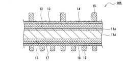
- FIG. 1 is a cross-sectional view showing a solar battery cell 10 which is an example of an embodiment.
- the solar battery cell 10 includes an n-type crystalline silicon wafer 11, a first passivation layer 12 formed on the light receiving surface of the n-type crystalline silicon wafer 11, and a first passivation layer. And an n-type crystalline silicon layer 13 formed.
- the solar cell 10 further includes a second passivation layer 16 formed on the back surface of the n-type crystalline silicon wafer 11 and a p-type amorphous silicon layer 17 formed on the second passivation layer 16.
- the “light-receiving surface” of the n-type crystalline silicon wafer 11 means a surface on which light is mainly incident (over 50% to 100%), and “back surface” is a surface opposite to the light-receiving surface. means.
- the crystallization rate of the p-type amorphous silicon layer 17 is lower than the crystallization rate of the n-type crystalline silicon layer 13, and the crystallization rate of the n-type crystalline silicon layer 13 is the crystal of the n-type crystalline silicon wafer 11. Lower than conversion rate.
- the crystallization ratio of the wafer and each layer is measured by the area ratio of the region where the Si crystal lattice occupies the observation region using a transmission electron microscope (TEM) in the cross section of the wafer and each layer shown in FIG. That is, the larger the length in the longitudinal direction of the Si crystal lattice region, the higher the crystallization rate of the wafer and each layer.
- TEM transmission electron microscope
- the n-type crystalline silicon wafer 11 is made of single crystal silicon
- the n-type crystalline silicon layer 13 is made of polycrystalline silicon.
- the region of the Si crystal lattice formed in the p-type amorphous silicon layer 17 preferably has a length in the longitudinal direction of less than 2 nm.
- the solar battery cell 10 includes a transparent conductive layer 14 formed on the n-type crystalline silicon layer 13 and a collector electrode 15 formed on the transparent conductive layer 14.
- the solar battery cell 10 includes a transparent conductive layer 18 formed on the p-type amorphous silicon layer 17 and a collector electrode 19 formed on the transparent conductive layer 18.
- the transparent conductive layer 14 and the collector electrode 15 constitute a light receiving surface electrode for collecting electrons generated in the n-type crystalline silicon wafer 11, and the transparent conductive layer 18 and the collector electrode 19 are positive electrodes generated in the n-type crystalline silicon wafer 11.
- a back electrode for collecting holes is constructed.
- Solar cell 10 includes a pair of electrodes formed on the light-receiving surface side and the back surface side of n-type crystalline silicon wafer 11.
- the n-type crystalline silicon wafer 11 may be an n-type polycrystalline silicon wafer, but is preferably an n-type single crystal silicon wafer.
- the concentration of the n-type dopant in the n-type crystalline silicon wafer 11 is, for example, 1 ⁇ 10 14 to 1 ⁇ 10 17 atoms / cm 3 .
- the n-type dopant is not particularly limited, but generally phosphorus (P) is used.
- the n-type crystalline silicon wafer 11 has a substantially square surface shape with one side of 120 to 160 mm, and the thickness of the n-type crystalline silicon wafer 11 is, for example, 50 to 300 ⁇ m.
- the substantially square includes, for example, an octagon in which short sides and long sides are alternately continuous and have two sets of long sides parallel to each other.
- a wafer manufactured by the Czochralski method (Cz method) is generally used, but a wafer manufactured by the epitaxial growth method can also be used.
- the n-type crystalline silicon wafer 11 does not substantially contain a p-type dopant such as boron. However, the end face of the n-type crystalline silicon wafer 11 and its vicinity may contain a p-type dopant.
- the concentration of the p-type dopant in the n-type crystalline silicon wafer 11 is 1 ⁇ 10 14 atoms / cm 3 or less, and the detection limit by secondary ion mass spectrometry (SIMS) is 1 ⁇ 10 15 atoms / cm 3 or less.
- the p-type amorphous silicon layer 17 is formed by a low temperature process, the diffusion of boron from the p-type amorphous silicon layer 17 to the n-type crystalline silicon wafer 11 does not substantially occur. For this reason, in the photovoltaic cell 10, the composite defect by the spreading
- the concentration of impurities at the interface in contact with the first passivation layer 12 and in the vicinity thereof is higher than the concentration of impurities at the interface in contact with the second passivation layer 16 and in the vicinity thereof.
- the interface in contact with the first passivation layer 12 of the n-type crystalline silicon wafer 11 may be referred to as “light-receiving surface side interface”, and the interface in contact with the second passivation layer 16 may be referred to as “back surface side interface”.
- Examples of impurities contained in the n-type crystalline silicon wafer 11 include oxygen, nitrogen, carbon and the like in addition to an n-type dopant such as phosphorus.
- the oxygen concentration at the light receiving surface side interface and its vicinity of the n-type crystalline silicon wafer 11 is higher than the oxygen concentration at the back surface side interface and its vicinity.
- the concentration of P, O, N, C, etc. contained in the n-type crystalline silicon wafer 11 is measured by SIMS or TEM-energy dispersive X-ray spectroscopy (TEM-EDX).
- a texture structure (not shown) is formed on the surface of the n-type crystalline silicon wafer 11.
- the texture structure is a surface uneven structure for increasing the light absorption amount of the n-type crystalline silicon wafer 11 by suppressing the surface reflection, and is provided on one of the light receiving surface and the back surface or on the light receiving surface and the back surface. Formed on both.
- the texture structure can be formed by anisotropic etching of the (100) plane of the single crystal silicon wafer using an alkaline solution, and the surface of the single crystal silicon wafer has a pyramidal uneven structure with the (111) plane as an inclined surface. It is formed.
- the height of the unevenness of the texture structure is, for example, 1 to 15 ⁇ m.
- the first passivation layer 12 is interposed between the light receiving surface of the n-type crystalline silicon wafer 11 and the n-type crystalline silicon layer 13, and suppresses carrier recombination on the light receiving surface side of the cell.
- a first passivation layer 12 is formed in substantially the entire area.
- the first passivation layer 12 formed over substantially the entire area may cover the entire surface of the approximately square or the end portion of the approximately square. The entire surface except the outer peripheral area of 2 mm or less may be covered.
- the first passivation layer 12 is preferably a layer having excellent thermal stability that does not impair passivation properties even when exposed to high temperatures.
- the first passivation layer 12 is preferably composed mainly of silicon oxide (SiO 2 ), silicon carbide (SiC), or silicon nitride (SiN).
- the thickness of the first passivation layer 12 is, for example, 0.1 to 5.0 nm.
- the thickness of the first passivation layer 12 is measured by observing a cross section of the cell using a TEM (the same applies to other layers).
- the oxygen concentration in the layer is preferably 1.0 ⁇ 10 21 atoms / cm 3 or more.
- the first passivation layer 12 has a higher oxygen concentration than the second passivation layer 16.
- the concentration of n-type dopants such as phosphorus in the first passivation layer 12 is higher than the concentration of p-type dopants such as boron in the second passivation layer 16.
- the formation process of the n-type crystalline silicon layer 13 is at a higher temperature than the formation process of the p-type amorphous silicon layer 17. Therefore, phosphorus in the n-type crystalline silicon layer 13 easily diffuses into the first passivation layer 12, but boron in the p-type amorphous silicon layer 17 hardly diffuses into the second passivation layer 16.
- the n-type crystalline silicon layer 13 is formed on the light receiving surface of the n-type crystalline silicon wafer 11 via the first passivation layer 12. On the light-receiving surface of the n-type crystalline silicon wafer 11, an n-type crystalline silicon layer 13 is formed over substantially the entire area via the first passivation layer 12.
- the thickness of the n-type crystalline silicon layer 13 is, for example, 5 to 20 nm, preferably 8 to 15 nm.
- the n-type crystalline silicon layer 13 is made of polycrystalline silicon or microcrystalline silicon doped n-type.
- the region of the Si crystal lattice formed in the n-type crystalline silicon layer 13 has a length in the longitudinal direction of 2 nm or more. If the region where the Si crystal lattice is observed is within this range, high sunlight transmittance can be obtained.
- the absorption coefficient in the wavelength range of 400 to 600 nm of the n-type crystalline silicon layer 13 is lower than the absorption coefficient of the p-type amorphous silicon layer 17, for example, 5 ⁇ 10 4 to 4 ⁇ 10 5 cm ⁇ at a wavelength of 420 nm. 1 .
- the absorption coefficient of each layer is determined by ellipsometry.
- the concentration of the n-type dopant in the n-type crystalline silicon layer 13 is, for example, 1 ⁇ 10 20 to 1 ⁇ 10 22 atoms / cm 3 , and preferably 3 ⁇ 10 20 to 5 ⁇ 10 21 atoms / cm 3 . .
- the n-type dopant is not particularly limited, but generally phosphorus is used.
- the n-type crystalline silicon layer 13 may contain the n-type dopant substantially uniformly, and a concentration gradient of the n-type dopant may exist.
- the resistivity of the n-type crystalline silicon layer 13 is higher than that of the transparent conductive layer 14 and is, for example, 0.1 to 150 m ⁇ ⁇ cm.
- the n-type crystalline silicon layer 13 has a lower hydrogen concentration than the p-type amorphous silicon layer 17. Further, the n-type crystalline silicon layer 13 has a lower hydrogen concentration than the second passivation layer 16.
- the hydrogen concentration in the n-type crystalline silicon layer 13 is, for example, 1 ⁇ 10 18 to 1 ⁇ 10 21 , and preferably 7 ⁇ 10 18 to 5 ⁇ 10 20 atoms / cm 3 .
- the refractive index of the n-type crystalline silicon layer 13 is preferably 2.5 times or more that of the transparent conductive layer 14, for example, 2.5 to 3.2. Is double.
- the refractive index of each layer is determined by a spectroscopic ellipsometer. If the refractive index of the n-type crystalline silicon layer 13 is within the above range, the color unevenness of the cell is reduced and a good appearance is obtained.
- the second passivation layer 16 is interposed between the back surface of the n-type crystalline silicon wafer 11 and the p-type amorphous silicon layer 17 and suppresses carrier recombination on the back surface side of the cell.
- a second passivation layer 16 is formed over substantially the entire area.
- the second passivation layer 16 formed over substantially the entire area may cover the entire surface of the approximately square or end portion of the approximately square. The entire surface except the outer peripheral area of 2 mm or less may be covered.
- the second passivation layer 16 is preferably a layer that can be formed at a temperature of about 200 ° C., and has lower thermal stability than the first passivation layer 12.
- a suitable second passivation layer 16 is substantially intrinsic amorphous silicon (hereinafter sometimes referred to as “i-type amorphous silicon”), or a non-conductive layer having a lower dopant concentration than the p-type amorphous silicon layer. It is a layer containing crystalline silicon.
- the thickness of the second passivation layer 16 is thicker than that of the first passivation layer 12, and is, for example, 5 to 10 nm.
- the second passivation layer 16 is preferably composed mainly of i-type amorphous silicon, and may be an i-type amorphous silicon layer substantially composed of only i-type amorphous silicon. . As described above, the second passivation layer 16 has a lower oxygen concentration than the first passivation layer 12, and the concentration of the p-type dopant such as boron in the second passivation layer 16 is n-type such as phosphorus in the first passivation layer 12. Lower than dopant concentration.
- the p-type amorphous silicon layer 17 is formed on the back surface of the n-type crystalline silicon wafer 11 via the second passivation layer 16.
- a p-type amorphous silicon layer 17 is formed in almost the entire region via the second passivation layer 16. Similar to the second passivation layer 16, the p-type amorphous silicon layer 17 formed over substantially the entire region may cover the entire surface of the substantially square, and the outer peripheral region of 2 mm or less is removed from the end of the approximately square. The entire surface may be covered.
- the thickness of the p-type amorphous silicon layer 17 is, for example, 1 to 25 nm, preferably 1 to 10 nm.
- the concentration of the p-type dopant in the p-type amorphous silicon layer 17 is, for example, 1 ⁇ 10 20 atoms / cm 3 or more.
- the p-type dopant is not particularly limited, but boron is generally used.
- the p-type amorphous silicon layer 17 contains, for example, boron substantially uniformly.
- the p-type amorphous silicon layer 17 has a higher hydrogen concentration than the n-type crystalline silicon layer 13.
- the transparent conductive layer 14 is formed over substantially the entire surface of the n-type crystalline silicon layer 13 on the light receiving surface side.
- the transparent conductive layer 18 is formed over substantially the entire area of the back surface of the p-type amorphous silicon layer 17.
- the transparent conductive layers 14 and 18 formed over substantially the entire area may cover the entire surface of the approximately square or the end of the approximately square. You may cover the whole surface except the outer peripheral area
- the transparent conductive layers 14 and 18 may be formed so as to cover them.
- the transparent conductive layers 14 and 18 are transparent in which a metal oxide such as indium oxide (In 2 O 3 ) or zinc oxide (ZnO) is doped with tungsten (W), tin (Sn), antimony (Sb), or the like. It is composed of a conductive oxide (IWO, ITO, etc.).
- the thickness of the transparent conductive layers 14 and 18 is preferably 30 to 500 nm, particularly preferably 50 to 200 nm.
- the collector electrodes 15 and 19 preferably each include a plurality of finger portions and a plurality of bus bar portions.
- the finger portion is a thin wire electrode formed over a wide area of the transparent conductive layers 14 and 18.
- the bus bar portion is a thin wire electrode that collects carriers from the finger portion, and is formed substantially orthogonal to each finger portion.
- the collector electrodes 15 and 19 are formed, for example, by applying a conductive paste on the transparent conductive layers 14 and 18 in a pattern including a large number of finger portions and two or three bus bar portions.
- the conductive paste for forming the collector electrodes 15 and 19 was formed by dispersing conductive particles having a diameter of 1 to 50 ⁇ m made of silver, copper, nickel or the like in a binder resin such as acrylic resin, epoxy resin, or phenol novolac. It may be a conductive paste.
- the collector electrode 19 is preferably formed in a larger area than the collector electrode 15, and the finger portions of the collector electrode 19 are formed more than the finger portions of the collector electrode 15. Therefore, the area of the transparent conductive layer 18 covered by the collector electrode 19 is larger than the area of the transparent conductive layer 14 covered by the collector electrode 15. Further, the collector electrode 15 is formed thicker than the collector electrode 19.
- the structure of the electrode is not particularly limited, and a metal layer may be formed over substantially the entire area of the transparent conductive layer 18 as a collecting electrode for the back electrode.
- FIG. 2 is a flowchart showing an example of the manufacturing process of the solar battery cell 10.
- the manufacturing process of the photovoltaic cell 10 includes the following processes. (1) A step of forming a first passivation layer 12 composed mainly of silicon oxide, silicon carbide, or silicon nitride on one surface of the n-type crystalline silicon wafer 11. (2) A step of forming an n-type crystalline silicon layer 13 on the first passivation layer 12. (3) A step of forming the second passivation layer 16 on the other surface of the n-type crystalline silicon wafer 11 on which the n-type crystalline silicon layer 13 is formed. (4) A step of forming a p-type amorphous silicon layer 17 on the second passivation layer 16.
- an oxide film composed mainly of silicon oxide is formed as the first passivation layer 12.
- a substantially intrinsic i-type amorphous silicon layer is formed thicker than the first passivation layer 12.
- the second passivation layer 16 may be a layer containing amorphous silicon having a p-type dopant concentration lower than that of the p-type amorphous silicon layer 17.
- an n-type crystalline silicon wafer 11 having a textured structure is prepared, and a silicon oxide film as the first passivation layer 12 is formed on the surface of the wafer (S1). ).
- a silicon oxide film as the first passivation layer 12 is formed on the surface of the wafer (S1). ).
- an n-type single crystal silicon wafer is preferably used as the n-type crystalline silicon wafer 11.
- the silicon oxide film is formed on both surfaces of the n-type single crystal silicon wafer.
- Examples of the silicon oxide film forming method include a steam oxidation method in which an n-type single crystal silicon wafer having a textured structure is heat-treated in a high-pressure steam atmosphere at about 500 ° C., and a nitric acid oxidation method in which the wafer is immersed in nitric acid.
- the silicon oxide film can be selectively formed only on one surface of the n-type crystalline silicon wafer 11.
- the oxide film removing step (S4) described later can be omitted.
- Examples of such an oxidation method include a plasma radical oxidation method and a method of forming a silicon oxide film (SiOx film) on one surface of the n-type crystalline silicon wafer 11 by CVD, sputtering, or the like.
- the oxygen concentration of the SiOx film can be adjusted by changing the film formation conditions.
- the first passivation layer 12 and the n-type crystalline silicon layer 13 can be formed by forming a SiOx film with a low oxygen concentration and doping the surface of the SiOx film and the vicinity of the surface with n-type.
- the first passivation layer 12 may be formed by forming an i-type amorphous silicon layer on one surface of the n-type crystalline silicon wafer 11 and oxidizing the i-type amorphous silicon layer. .
- an n-type crystalline silicon layer 13 is formed on the silicon oxide film (S2).
- the n-type crystalline silicon layer 13 is formed by, for example, CVD or sputtering under a high temperature condition of 400 to 900 ° C.
- CVD for example, a source gas diluted with hydrogen by adding phosphine (PH 3 ) to silane gas (SiH 4 ) is used.
- phosphine PH 3
- silane gas SiH 4
- the dopant concentration of the n-type amorphous silicon layer can be adjusted by changing the mixed concentration of phosphine.
- the n-type crystalline silicon layer 13 is formed as an n-type doped microcrystalline or polycrystalline silicon layer.
- hydrogen (H 2 ) sintering is performed on the n-type crystalline silicon wafer 11 on which the n-type crystalline silicon layer 13 is formed (S3).
- the hydrogen sintering is performed, for example, by heat-treating the n-type crystalline silicon wafer 11 at a temperature of about 350 to 450 ° C. in a forming gas obtained by diluting hydrogen gas with an inert gas such as nitrogen gas.
- this step makes it possible to replenish hydrogen that has escaped from one surface of the n-type crystalline silicon wafer 11 exposed to a high temperature during the formation of the n-type crystalline silicon layer 13 and the vicinity thereof. If the hydrogen concentration of the n-type crystalline silicon layer 13 is sufficiently high that it is not necessary to replenish, the hydrogen sintering step of S3 may be omitted.
- an i-type silicon layer which is the second passivation layer 16 on the other surface of the wafer is formed in order (S5, S6).
- the silicon oxide film on the other surface of the n-type crystalline silicon wafer 11 immerses the n-type crystalline silicon wafer 11 having the n-type crystalline silicon layer 13 formed on one surface in hydrofluoric acid (HF). Is removed.
- HF hydrofluoric acid
- the i-type amorphous silicon layer and the p-type amorphous silicon layer 17 are formed by CVD or sputtering with a clean n-type crystalline silicon wafer 11 placed in a vacuum chamber.
- a source gas obtained by diluting a silane gas with hydrogen (H 2 ) is used for forming the i-type amorphous silicon layer by CVD.
- a source gas diluted with hydrogen by adding diborane (B 2 H 6 ) to a silane gas is used.
- the dopant concentration of the p-type amorphous silicon layer 17 can be adjusted by changing the mixed concentration of diborane.
- transparent conductive layers 14 and 18 are respectively formed on the n-type crystalline silicon layer 13 and the p-type amorphous silicon layer 17 (S7).
- collector electrodes 15 and 19 are formed on the transparent conductive layers 14 and 18, respectively (S8).
- the transparent conductive layers 14 and 18 are formed by sputtering, for example.
- the collector electrodes 15 and 19 are formed, for example, by applying a conductive paste containing silver (Ag) particles on each transparent conductive layer by screen printing or the like.
- the solar cell 10 provided with the n-type crystalline silicon layer 13 on the light-receiving surface side of the crystalline silicon wafer 11 and the p-type crystalline silicon layer 17 on the back surface side has a low manufacturing cost, and High output characteristics.
- the solar battery cell 10 has a good appearance with little or no color unevenness and excellent durability.
- FIG. 3 is a cross-sectional view illustrating a solar battery cell 10A that is another example of the embodiment.
- the solar cell 10A has an n + -type doped n + layer 11a at and near the interface in contact with the first passivation layer 12 of the n-type crystalline silicon wafer 11A.
- the n + layer 11a is formed by diffusing an n-type dopant such as phosphorus from the light receiving surface side of the n-type crystalline silicon wafer 11A, and the concentration of the n-type dopant is higher than that of other regions of the wafer.
- the n-type crystalline silicon wafer 11A is substantially free of p-type dopants such as boron, as in the case of the solar battery cell 10.
- the concentration of the n-type dopant in the n + layer 11a is, for example, 1 ⁇ 10 17 to 1 ⁇ 10 20 atoms / cm 3 and is formed with a thickness of 1 ⁇ m or less from the light-receiving surface side interface of the n-type crystalline silicon wafer 11A.
- the n-type crystalline silicon wafer 11A has a region where the dopant concentration is equal to or higher than the dopant concentration at the central portion in the thickness direction of the n-type crystalline silicon wafer 11A only in the thickness range of 1 ⁇ m or less from the light receiving surface.
- the n + layer 11a generally has a concentration gradient in which the concentration of the n-type dopant decreases as the depth increases, that is, the distance from the light receiving surface of the n-type crystalline silicon wafer 11A increases.
- the n-type dopant concentration gradient also exists in the n-type crystalline silicon layer 13.
- the n-type crystalline silicon layer 13 has a concentration gradient in which the concentration of the n-type dopant increases as it approaches the first passivation layer 12.
- it has a concentration gradient in which the concentration of the n-type dopant decreases as it approaches the first passivation layer 12.
- FIG. 4 is a flowchart showing an example of the manufacturing process of the solar battery cell 10A.
- S2 silicon oxide film
- S3 N 2 annealing treatment
- the n + layer 11 a is formed by doping the light-receiving surface side interface of the n-type crystalline silicon wafer 11 and its vicinity to n-type. It is formed.
- the n + layer 11a is formed by diffusing the n-type dopant in the n-type amorphous silicon layer by the N 2 annealing treatment. Processes other than S2 and S3 are the same as the manufacturing process of the solar battery cell 10.
- the n-type crystalline silicon wafer 11 on which the silicon oxide film is formed is placed in a vacuum chamber, and an n-type amorphous silicon layer is formed by CVD or sputtering.
- an n-type amorphous silicon layer is formed by CVD or sputtering.
- CVD for example, a source gas diluted with hydrogen by adding phosphine to silane gas is used.
- S3 is a step of heat-treating the n-type crystalline silicon wafer 11 on which the n-type amorphous silicon layer is formed at a high temperature of about 800 to 900 ° C. in a nitrogen atmosphere.
- S3 it is also possible to perform a high temperature / low oxygen atmosphere annealing process using an inert gas other than nitrogen, or laser annealing.
- crystallization of the n-type amorphous silicon layer proceeds, and an n-type polycrystalline silicon layer that is the n-type crystalline silicon layer 13 is formed.
- an n-type dopant such as phosphorus contained in the n-type amorphous silicon layer diffuses into the n-type crystalline silicon wafer 11, and an n + layer 11a is formed at and near the light-receiving surface side interface.
- the n + layer 11a can also be formed by a thermal diffusion method using vapor such as phosphoryl chloride (POCl 3 ).
- a SiOx film having a low oxygen concentration or an i-type amorphous silicon layer is formed on one surface of the n-type crystalline silicon wafer 11, and phosphorus is thermally diffused at a high temperature of about 800 to 900 ° C.
- An n + layer 11a and an n-type crystalline silicon layer 13 may be formed.
- an n-type crystalline silicon layer 13 is formed by forming a SiOx film on one surface of the n-type crystalline silicon wafer 11, applying liquid silicon on the SiOx film, and performing N 2 annealing treatment. It is also possible.
- FIG. 5 is a cross-sectional view illustrating a solar battery cell 30 which is another example of the embodiment.
- the solar battery cell 30 includes electrodes on the light receiving surface side and the back surface side of the n-type crystalline silicon wafer in that the electrode is provided only on the back surface side of the n-type crystalline silicon wafer 31.
- the n-type crystalline silicon wafer 31 has an n + layer 31a doped n-type at and near the interface in contact with the first passivation layer 32.
- the solar battery cell 30 includes a first passivation layer 32 formed on the light receiving surface of an n-type crystalline silicon wafer 31 and an n-type crystalline silicon layer 33 formed on the first passivation layer 32.
- the solar battery cell 30 has a protective layer 34 on the n-type crystalline silicon layer 33.
- the protective layer 34 protects, for example, the n-type crystalline silicon layer 33 and suppresses reflection of sunlight on the cell surface.
- the protective layer 34 is preferably made of a material having high light transmittance, and is made of, for example, an insulator such as silicon oxide, silicon nitride, or silicon oxynitride as a main component.
- Solar cell 30 includes second passivation layers 35 and 37 formed on the back side of n-type crystalline silicon wafer 31, p-type amorphous silicon layer 36, and n-type amorphous silicon layer 38. .
- the second passivation layer 35 is formed on the back surface of the n-type crystalline silicon wafer 31 and is interposed between the n-type crystalline silicon wafer 31 and the p-type amorphous silicon layer 36.
- the second passivation layer 37 is formed on the back surface of the n-type crystalline silicon wafer 31 and is interposed between the n-type crystalline silicon wafer 31 and the n-type amorphous silicon layer 38.
- the p-type amorphous silicon layer 36 and the n-type amorphous silicon layer 38 form a p-type region and an n-type region on the back side of the n-type crystalline silicon wafer 31, respectively.
- the second passivation layer 35 and the p-type amorphous silicon layer 36 constitute a p-type region
- the second passivation layer 37 and the n-type amorphous silicon layer 38 constitute an n-type region.
- the area of the p-type region formed on the back surface of the n-type crystalline silicon wafer 31 is preferably larger than the area of the n-type region.
- the p-type region and the n-type region are alternately arranged in one direction and are formed in a comb-like pattern in plan view that meshes with each other.
- a part of the p-type region overlaps a part of the n-type region, and the p-type region and the n-type region are formed on the back surface of the n-type crystalline silicon wafer 31 without a gap.
- An insulating layer 39 is provided between the regions where the p-type region and the n-type region overlap.
- the insulating layer 39 is composed mainly of, for example, silicon oxide, silicon nitride, or silicon oxynitride.
- the insulating layer 39 may be made of the same material as the protective layer 34.
- a configuration similar to that of the p-type amorphous silicon layer 17 of the solar battery cells 10 and 10A can be applied to the second passivation layers 35 and 37. Also, the same configuration as that of the p-type amorphous silicon layer 17 of the solar cells 10 and 10A can be applied to the p-type amorphous silicon layer 36.
- the n-type amorphous silicon layer 38 is an n-type doped amorphous silicon layer.
- the n-type dopant concentration in the n-type amorphous silicon layer 38 is, for example, 1 ⁇ 10 20 atoms / cm 3 or more.
- the n-type amorphous silicon layer 38 generally contains an n-type dopant substantially uniformly.
- the n-type dopant is not particularly limited, but generally phosphorus is used.
- the p-type amorphous silicon layer 36 and the n-type amorphous silicon layer 38 have a higher hydrogen concentration and lower density than the n-type crystalline silicon layer 33.
- the solar cell 30 includes a transparent conductive layer 40 and a collector electrode 41 formed on the p-type amorphous silicon layer 36, and a transparent conductive layer 42 and a collector electrode 43 formed on the n-type amorphous silicon layer 38.
- the transparent conductive layer 40 and the collector electrode 41 are p-side electrodes formed on the p-type region, and the transparent conductive layer 42 and the collector electrode 43 are n-side electrodes formed on the n-type region.
- the transparent conductive layers 40 and 42 are separated from each other at a position corresponding to the insulating layer 39.
- the collecting electrodes 41 and 43 are formed on the transparent conductive layers 40 and 42, respectively.
- the collector electrodes 41 and 43 may be formed using a conductive paste, but are preferably formed by electrolytic plating.
- the collector electrodes 41 and 43 are made of, for example, a metal such as nickel (Ni), copper (Cu), silver (Ag), etc., and may have a stacked structure of a Ni layer and a Cu layer, in order to improve corrosion resistance. You may have a tin (Sn) layer in the outermost surface.
- the solar battery cell 30 includes a first passivation layer 32, an n-type crystalline silicon layer 33, and an n + layer 31a on the light-receiving surface side of the n-type crystalline silicon wafer 31 by a method similar to that of the solar battery cell 10A. Can be formed.
- the protective layer 34, the p-type region, the n-type region, the insulating layer 39, the transparent conductive layers 40 and 42, and the collector electrodes 41 and 43 are formed by a method similar to that of a conventionally known solar battery cell having electrodes only on the back surface side. it can. Similar to the solar battery cells 10 and 10A, the solar battery cell 30 is low in manufacturing cost, has high output characteristics, has a good appearance, and is excellent in durability.
Priority Applications (4)
| Application Number | Priority Date | Filing Date | Title |
|---|---|---|---|
| JP2018501077A JP6719099B2 (ja) | 2016-02-22 | 2017-01-26 | 太陽電池セルおよび太陽電池セルの製造方法 |
| CN201780012714.6A CN108701736A (zh) | 2016-02-22 | 2017-01-26 | 太阳能单电池和太阳能单电池的制造方法 |
| EP17756075.2A EP3422422A4 (en) | 2016-02-22 | 2017-01-26 | SOLAR BATTERY ELEMENT AND METHOD FOR MANUFACTURING SOLAR BATTERY ELEMENT |
| US16/101,788 US20190006534A1 (en) | 2016-02-22 | 2018-08-13 | Solar cell and method for manufacturing solar cell |
Applications Claiming Priority (2)
| Application Number | Priority Date | Filing Date | Title |
|---|---|---|---|
| JP2016031090 | 2016-02-22 | ||
| JP2016-031090 | 2016-02-22 |
Related Child Applications (1)
| Application Number | Title | Priority Date | Filing Date |
|---|---|---|---|
| US16/101,788 Continuation US20190006534A1 (en) | 2016-02-22 | 2018-08-13 | Solar cell and method for manufacturing solar cell |
Publications (1)
| Publication Number | Publication Date |
|---|---|
| WO2017145633A1 true WO2017145633A1 (ja) | 2017-08-31 |
Family
ID=59685465
Family Applications (1)
| Application Number | Title | Priority Date | Filing Date |
|---|---|---|---|
| PCT/JP2017/002736 WO2017145633A1 (ja) | 2016-02-22 | 2017-01-26 | 太陽電池セルおよび太陽電池セルの製造方法 |
Country Status (5)
| Country | Link |
|---|---|
| US (1) | US20190006534A1 (zh) |
| EP (1) | EP3422422A4 (zh) |
| JP (1) | JP6719099B2 (zh) |
| CN (1) | CN108701736A (zh) |
| WO (1) | WO2017145633A1 (zh) |
Cited By (3)
| Publication number | Priority date | Publication date | Assignee | Title |
|---|---|---|---|---|
| CN111052401A (zh) * | 2017-12-14 | 2020-04-21 | 株式会社钟化 | 光电转换元件和光电转换装置 |
| US11621359B1 (en) | 2022-04-11 | 2023-04-04 | Zhejiang Jinko Solar Co., Ltd. | Solar cell, photovoltaic module, and method for preparing the solar cell |
| JP7336569B1 (ja) | 2022-04-11 | 2023-08-31 | ジョジアン ジンコ ソーラー カンパニー リミテッド | 太陽電池およびその製造方法、光起電力モジュール |
Families Citing this family (6)
| Publication number | Priority date | Publication date | Assignee | Title |
|---|---|---|---|---|
| JP2022543358A (ja) | 2019-08-09 | 2022-10-12 | リーディング エッジ イクウィップメント テクノロジーズ インコーポレイテッド | 酸素濃度の低い領域を有するリボンまたはウェハの製造 |
| JP2021044384A (ja) * | 2019-09-11 | 2021-03-18 | パナソニック株式会社 | 太陽電池セル |
| CN112018208B (zh) * | 2020-08-06 | 2022-10-04 | 隆基绿能科技股份有限公司 | 一种太阳能电池及制备方法 |
| CN112768549A (zh) | 2021-02-09 | 2021-05-07 | 通威太阳能(成都)有限公司 | 一种高光电转换效率的hjt电池及其制备方法 |
| CN112802910A (zh) * | 2021-02-09 | 2021-05-14 | 通威太阳能(成都)有限公司 | 一种高效硅异质结太阳能电池及其制备方法 |
| CN114122154B (zh) * | 2021-10-11 | 2023-12-19 | 中国科学院电工研究所 | 一种载流子选择性钝化接触太阳电池及其制备方法 |
Citations (6)
| Publication number | Priority date | Publication date | Assignee | Title |
|---|---|---|---|---|
| JP2005135986A (ja) * | 2003-10-28 | 2005-05-26 | Kaneka Corp | 積層型光電変換装置 |
| JP2011003639A (ja) * | 2009-06-17 | 2011-01-06 | Kaneka Corp | 結晶シリコン系太陽電池とその製造方法 |
| JP2012060080A (ja) * | 2010-09-13 | 2012-03-22 | Ulvac Japan Ltd | 結晶太陽電池及びその製造方法 |
| JP2013211392A (ja) * | 2012-03-30 | 2013-10-10 | Sanyo Electric Co Ltd | 半導体装置の製造方法 |
| JP2014216334A (ja) * | 2013-04-22 | 2014-11-17 | 長州産業株式会社 | 光発電素子 |
| WO2015060012A1 (ja) * | 2013-10-25 | 2015-04-30 | シャープ株式会社 | 光電変換素子 |
Family Cites Families (5)
| Publication number | Priority date | Publication date | Assignee | Title |
|---|---|---|---|---|
| US20090211623A1 (en) * | 2008-02-25 | 2009-08-27 | Suniva, Inc. | Solar module with solar cell having crystalline silicon p-n homojunction and amorphous silicon heterojunctions for surface passivation |
| KR101030447B1 (ko) * | 2009-02-27 | 2011-04-25 | 성균관대학교산학협력단 | 이종접합 실리콘 태양전지와 그 제조방법 |
| CN102460715B (zh) * | 2009-04-21 | 2015-07-22 | 泰特拉桑有限公司 | 高效率太阳能电池结构及制造方法 |
| CN201699034U (zh) * | 2010-01-28 | 2011-01-05 | 上海超日太阳能科技股份有限公司 | 一种硅基异质结太阳电池 |
| FR2996058B1 (fr) * | 2012-09-24 | 2014-09-26 | Commissariat Energie Atomique | Cellule photovoltaique a hererojonction et procede de fabrication d'une telle cellule |
-
2017
- 2017-01-26 JP JP2018501077A patent/JP6719099B2/ja active Active
- 2017-01-26 EP EP17756075.2A patent/EP3422422A4/en not_active Withdrawn
- 2017-01-26 WO PCT/JP2017/002736 patent/WO2017145633A1/ja active Application Filing
- 2017-01-26 CN CN201780012714.6A patent/CN108701736A/zh active Pending
-
2018
- 2018-08-13 US US16/101,788 patent/US20190006534A1/en not_active Abandoned
Patent Citations (6)
| Publication number | Priority date | Publication date | Assignee | Title |
|---|---|---|---|---|
| JP2005135986A (ja) * | 2003-10-28 | 2005-05-26 | Kaneka Corp | 積層型光電変換装置 |
| JP2011003639A (ja) * | 2009-06-17 | 2011-01-06 | Kaneka Corp | 結晶シリコン系太陽電池とその製造方法 |
| JP2012060080A (ja) * | 2010-09-13 | 2012-03-22 | Ulvac Japan Ltd | 結晶太陽電池及びその製造方法 |
| JP2013211392A (ja) * | 2012-03-30 | 2013-10-10 | Sanyo Electric Co Ltd | 半導体装置の製造方法 |
| JP2014216334A (ja) * | 2013-04-22 | 2014-11-17 | 長州産業株式会社 | 光発電素子 |
| WO2015060012A1 (ja) * | 2013-10-25 | 2015-04-30 | シャープ株式会社 | 光電変換素子 |
Non-Patent Citations (1)
| Title |
|---|
| See also references of EP3422422A4 * |
Cited By (6)
| Publication number | Priority date | Publication date | Assignee | Title |
|---|---|---|---|---|
| CN111052401A (zh) * | 2017-12-14 | 2020-04-21 | 株式会社钟化 | 光电转换元件和光电转换装置 |
| CN111052401B (zh) * | 2017-12-14 | 2023-03-21 | 株式会社钟化 | 光电转换元件和光电转换装置 |
| US11621359B1 (en) | 2022-04-11 | 2023-04-04 | Zhejiang Jinko Solar Co., Ltd. | Solar cell, photovoltaic module, and method for preparing the solar cell |
| JP7336569B1 (ja) | 2022-04-11 | 2023-08-31 | ジョジアン ジンコ ソーラー カンパニー リミテッド | 太陽電池およびその製造方法、光起電力モジュール |
| JP2023155863A (ja) * | 2022-04-11 | 2023-10-23 | ジョジアン ジンコ ソーラー カンパニー リミテッド | 太陽電池およびその製造方法、光起電力モジュール |
| US11862741B2 (en) | 2022-04-11 | 2024-01-02 | Zhejiang Jinko Solar Co., Ltd. | Solar cell, photovoltaic module, and method for preparing the solar cell |
Also Published As
| Publication number | Publication date |
|---|---|
| CN108701736A (zh) | 2018-10-23 |
| EP3422422A1 (en) | 2019-01-02 |
| JP6719099B2 (ja) | 2020-07-08 |
| JPWO2017145633A1 (ja) | 2018-11-29 |
| EP3422422A4 (en) | 2019-02-27 |
| US20190006534A1 (en) | 2019-01-03 |
Similar Documents
| Publication | Publication Date | Title |
|---|---|---|
| JP6719099B2 (ja) | 太陽電池セルおよび太陽電池セルの製造方法 | |
| WO2018025643A1 (ja) | 太陽電池セルおよび太陽電池セルの製造方法 | |
| KR20100015622A (ko) | 태양 전지 | |
| TW201432925A (zh) | 矽晶太陽能電池結構 | |
| JP6893331B2 (ja) | 太陽電池 | |
| JP5602251B2 (ja) | 透明電極基板およびその製造方法、光電変換装置およびその製造方法、光電変換モジュール | |
| JP7228561B2 (ja) | 太陽電池の製造方法 | |
| JP6109107B2 (ja) | 太陽電池およびその製造方法 | |
| JP5745653B2 (ja) | 光起電力装置およびその製造方法、光起電力モジュール | |
| TWI427808B (zh) | Production method of back electrode solar cell | |
| JP6785477B2 (ja) | 太陽電池セルおよび太陽電池セルの製造方法 | |
| CN111403551A (zh) | 一种高效单晶硅perc太阳能电池的制备方法 | |
| JPWO2019163648A1 (ja) | 太陽電池の製造方法 | |
| JP5645734B2 (ja) | 太陽電池素子 | |
| CN110120434B (zh) | 电池片及其制备方法 | |
| JP2021057436A (ja) | 太陽電池セル | |
| JP2021057435A (ja) | 太陽電池セルおよび太陽電池セルの製造方法 | |
| TWI681566B (zh) | 太陽能電池以及其製造方法 | |
| WO2019004126A1 (ja) | 光電変換装置の製造方法 | |
| JP5398772B2 (ja) | 光起電力装置およびその製造方法、光起電力モジュール | |
| KR102024084B1 (ko) | 태양 전지 및 이의 제조 방법 |
Legal Events
| Date | Code | Title | Description |
|---|---|---|---|
| WWE | Wipo information: entry into national phase |
Ref document number: 2018501077 Country of ref document: JP |
|
| NENP | Non-entry into the national phase |
Ref country code: DE |
|
| WWE | Wipo information: entry into national phase |
Ref document number: 2017756075 Country of ref document: EP |
|
| ENP | Entry into the national phase |
Ref document number: 2017756075 Country of ref document: EP Effective date: 20180924 |
|
| 121 | Ep: the epo has been informed by wipo that ep was designated in this application |
Ref document number: 17756075 Country of ref document: EP Kind code of ref document: A1 |