WO2017086481A1 - 磁気トンネル接合素子及び磁気メモリ - Google Patents
磁気トンネル接合素子及び磁気メモリ Download PDFInfo
- Publication number
- WO2017086481A1 WO2017086481A1 PCT/JP2016/084372 JP2016084372W WO2017086481A1 WO 2017086481 A1 WO2017086481 A1 WO 2017086481A1 JP 2016084372 W JP2016084372 W JP 2016084372W WO 2017086481 A1 WO2017086481 A1 WO 2017086481A1
- Authority
- WO
- WIPO (PCT)
- Prior art keywords
- layer
- protective layer
- tunnel junction
- magnetic
- magnetic tunnel
- Prior art date
- Legal status (The legal status is an assumption and is not a legal conclusion. Google has not performed a legal analysis and makes no representation as to the accuracy of the status listed.)
- Ceased
Links
Images


Classifications
-
- H—ELECTRICITY
- H10—SEMICONDUCTOR DEVICES; ELECTRIC SOLID-STATE DEVICES NOT OTHERWISE PROVIDED FOR
- H10N—ELECTRIC SOLID-STATE DEVICES NOT OTHERWISE PROVIDED FOR
- H10N50/00—Galvanomagnetic devices
- H10N50/10—Magnetoresistive devices
-
- G—PHYSICS
- G11—INFORMATION STORAGE
- G11C—STATIC STORES
- G11C11/00—Digital stores characterised by the use of particular electric or magnetic storage elements; Storage elements therefor
- G11C11/02—Digital stores characterised by the use of particular electric or magnetic storage elements; Storage elements therefor using magnetic elements
- G11C11/16—Digital stores characterised by the use of particular electric or magnetic storage elements; Storage elements therefor using magnetic elements using elements in which the storage effect is based on magnetic spin effect
- G11C11/161—Digital stores characterised by the use of particular electric or magnetic storage elements; Storage elements therefor using magnetic elements using elements in which the storage effect is based on magnetic spin effect details concerning the memory cell structure, e.g. the layers of the ferromagnetic memory cell
-
- G—PHYSICS
- G11—INFORMATION STORAGE
- G11C—STATIC STORES
- G11C11/00—Digital stores characterised by the use of particular electric or magnetic storage elements; Storage elements therefor
- G11C11/02—Digital stores characterised by the use of particular electric or magnetic storage elements; Storage elements therefor using magnetic elements
- G11C11/16—Digital stores characterised by the use of particular electric or magnetic storage elements; Storage elements therefor using magnetic elements using elements in which the storage effect is based on magnetic spin effect
- G11C11/165—Auxiliary circuits
- G11C11/1673—Reading or sensing circuits or methods
-
- G—PHYSICS
- G11—INFORMATION STORAGE
- G11C—STATIC STORES
- G11C11/00—Digital stores characterised by the use of particular electric or magnetic storage elements; Storage elements therefor
- G11C11/02—Digital stores characterised by the use of particular electric or magnetic storage elements; Storage elements therefor using magnetic elements
- G11C11/16—Digital stores characterised by the use of particular electric or magnetic storage elements; Storage elements therefor using magnetic elements using elements in which the storage effect is based on magnetic spin effect
- G11C11/165—Auxiliary circuits
- G11C11/1675—Writing or programming circuits or methods
-
- G—PHYSICS
- G11—INFORMATION STORAGE
- G11C—STATIC STORES
- G11C11/00—Digital stores characterised by the use of particular electric or magnetic storage elements; Storage elements therefor
- G11C11/02—Digital stores characterised by the use of particular electric or magnetic storage elements; Storage elements therefor using magnetic elements
- G11C11/16—Digital stores characterised by the use of particular electric or magnetic storage elements; Storage elements therefor using magnetic elements using elements in which the storage effect is based on magnetic spin effect
- G11C11/165—Auxiliary circuits
- G11C11/1695—Protection circuits or methods
-
- H—ELECTRICITY
- H10—SEMICONDUCTOR DEVICES; ELECTRIC SOLID-STATE DEVICES NOT OTHERWISE PROVIDED FOR
- H10B—ELECTRONIC MEMORY DEVICES
- H10B61/00—Magnetic memory devices, e.g. magnetoresistive RAM [MRAM] devices
-
- H—ELECTRICITY
- H10—SEMICONDUCTOR DEVICES; ELECTRIC SOLID-STATE DEVICES NOT OTHERWISE PROVIDED FOR
- H10D—INORGANIC ELECTRIC SEMICONDUCTOR DEVICES
- H10D84/00—Integrated devices formed in or on semiconductor substrates that comprise only semiconducting layers, e.g. on Si wafers or on GaAs-on-Si wafers
- H10D84/80—Integrated devices formed in or on semiconductor substrates that comprise only semiconducting layers, e.g. on Si wafers or on GaAs-on-Si wafers characterised by the integration of at least one component covered by groups H10D12/00 or H10D30/00, e.g. integration of IGFETs
-
- H—ELECTRICITY
- H10—SEMICONDUCTOR DEVICES; ELECTRIC SOLID-STATE DEVICES NOT OTHERWISE PROVIDED FOR
- H10N—ELECTRIC SOLID-STATE DEVICES NOT OTHERWISE PROVIDED FOR
- H10N50/00—Galvanomagnetic devices
- H10N50/80—Constructional details
-
- H—ELECTRICITY
- H10—SEMICONDUCTOR DEVICES; ELECTRIC SOLID-STATE DEVICES NOT OTHERWISE PROVIDED FOR
- H10N—ELECTRIC SOLID-STATE DEVICES NOT OTHERWISE PROVIDED FOR
- H10N50/00—Galvanomagnetic devices
- H10N50/80—Constructional details
- H10N50/85—Materials of the active region
Definitions
- the present invention relates to a magnetic tunnel junction element and a magnetic memory.
- Patent Document 1 discloses an MTJ element having a structure (double interface structure) in which a recording layer made of CoFeB is sandwiched between a barrier layer (MgO) containing oxygen and a protective layer (MgO).
- An MTJ element having a double interface structure is also disclosed in Patent Document 2 (paragraph 0011, FIG. 1).
- the protective layer of the MTJ element disclosed in Patent Document 2 is composed of a conductive oxide layer.
- Patent Document 2 further discloses a configuration in which the metal cap layer 13 is formed on the oxide cap layer 31 (protective layer).
- the MTJ elements described in Patent Documents 1 and 2 can exhibit sufficient characteristics in the current technology generation. However, when the MTJ element is further downsized, there is a possibility that sufficient characteristics cannot be obtained.
- the performance of the MTJ element is expressed by the tunnel magnetoresistance ratio TMR, the thermal stability ⁇ , and the threshold current.
- Rp is the resistance value of the current path of the MTJ element when the magnetizations of the reference layer and the free layer adjacent to the barrier film are arranged in parallel
- Rap is the magnetization of the reference layer and the free layer adjacent to the barrier film antiparallel. This is the resistance value of the current path when arranged.
- the thermal stability ⁇ is substantially proportional to Keff ⁇ V / kBT.
- Keff effective magnetic anisotropy energy density
- V volume
- kB Boltzmann constant
- T absolute temperature
- a data retention period of 10 years or more is required.
- a thermal stability ⁇ of 80 or more is required.
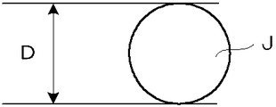
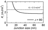
- it is necessary to ensure the size (diameter) and thermal stability ⁇ 80 of the joint surface when the joint surface of the magnetic tunnel junction of the ferromagnetic electrode formed from CoFeB and the MgO layer is circular. The relationship with the interface magnetic anisotropy is shown in FIG.
- the size of the bonding surface is 30 nm or less
- an interface magnetic anisotropy of 2.5 [mJ / m 2 ] or more is required.
- the present invention has been made in view of the above circumstances, and an object thereof is to provide a magnetic tunnel junction element and a magnetic memory with higher thermal stability.
- the magnetic tunnel junction device of the present invention comprises: A reference layer composed of a ferromagnetic material; A barrier layer comprising O; A recording layer composed of a ferromagnetic material containing Co or Fe; A first protective layer comprising O; A second protective layer comprising at least one of Pt, Ru, Co, Fe, CoB, FeB or CoFeB; Are laminated.
- the second protective layer is composed of a layer containing at least one Pt or Ru, for example, and has a thickness of 0.3 to 3.5 nm.
- the second protective layer is composed of a layer containing at least one of Co, Fe, CoB, FeB or CoFeB, for example, and has a thickness of 0.1 to 3.5 nm.
- At least one of a bonding surface between the reference layer and the barrier layer, a bonding surface between the barrier layer and the recording layer, and a bonding surface between the recording layer and the first protective layer has a diameter of 30 nm.
- the joint surface is smaller than the area of the circle.
- the recording layer has a magnetization direction perpendicular to the interface due to, for example, magnetic anisotropy at the interface with the barrier layer or the first protective layer that is in contact with the recording layer.
- the magnetic tunnel junction element has Ru, Rh, Pd, Cu, Ir, Au, Ta, Hf, W, Zr, Nb, Mo, Ti, V, Cr, or an alloy thereof on the second protective layer. You may provide the 3rd protective layer containing.
- the second protective layer has a thickness of 0.6 to 1.5 nm, for example.
- the second protective layer preferably has a thickness of 0.6 to 1.0 nm.
- the second protective layer is preferably a non-magnetic material.
- the second protective layer has magnetism, and the magnetic tunnel junction element is formed on the non-magnetic layer formed on the second protective layer, on the non-magnetic layer, and And a ferromagnetic layer magnetized in the opposite direction parallel to the magnetization direction of the two protective layers.
- the second protective layer has a thickness of 0.6 to 3.5 nm, for example.
- the ferromagnetic layer includes, for example, at least one of Co, Fe, CoB, FeB, CoFeB, CoPt alloy, CoPd alloy, FePt alloy, FePd alloy, and ferrimagnetic material.
- the magnetic memory according to the present invention is: A memory cell comprising the magnetic tunnel junction element described above; A write circuit for selecting the memory cell and writing data; A read circuit for selecting the memory cell and reading data; Is provided.
- a magnetic tunnel junction element with high thermal stability and a magnetic memory using the same can be obtained.
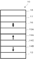
- FIG. 1 is a diagram illustrating a configuration of a magnetic memory circuit including an MTJ element according to a first embodiment.
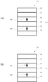
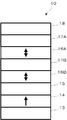
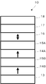
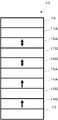
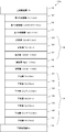
- FIG. 1 and (B) are diagrams for explaining the parallel state (low resistance state) and antiparallel state (high resistance state) of magnetization of the recording layer adjacent to the barrier layer of the MTJ element and the reference layer. . It is a figure which shows the modification of the MTJ element shown in FIG. It is a figure which shows the modification of the MTJ element shown in FIG. It is a figure which shows the modification of the MTJ element shown in FIG. It is a figure which shows the modification of the MTJ element shown in FIG. It is a figure which shows the modification of the MTJ element shown in FIG. It is a figure which shows the structure of the MTJ element based on Embodiment 2 of this invention.
- FIG. 12 It is a figure which shows the relationship between the film thickness of the 2nd protective layer of the MTJ element shown in FIG. 12, and the magnitude
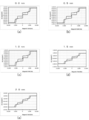
- (A) to (e) show the relationship between the strength of the magnetic field when the magnetic field is applied perpendicularly to the layer surface of the MTJ element shown in FIG. 12 and the magnitude of the magnetization of the recording layer for each film thickness of the second protective layer.
- FIG. (A) to (e) show the relationship between the strength of the magnetic field and the magnitude of magnetization of the MTJ element when a magnetic field is applied perpendicularly to the layer surface of the MTJ element shown in FIG. FIG. FIG.
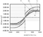
- FIG. 13 is a diagram showing the relationship between the strength of the applied magnetic field and the magnitude of magnetization of the recording layer when the second protective layer of the MTJ element shown in FIG. 12 is formed of a different material and a magnetic field is applied from the outside perpendicular to the layer surface. is there.
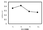
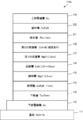
- the third protective layer of the MTJ element shown in FIG. 12 is formed of a different material, the presence / absence of the third protective layer, the material, the magnetic anisotropy of the recording layer, and the product of the film thickness (Keff ⁇ t) It is a figure which shows a relationship. It is a figure which shows the structure of the MTJ element which concerns on Embodiment 3 of this invention. It is a graph which shows the relationship between the size of a magnetic tunnel junction, and the magnitude
- size of interface magnetic anisotropy required in order to ensure thermal stability 80.
- a magnetic tunnel junction element (MTJ (Magnetic Tunnel Junction) element) 10 has a magnetic tunnel junction exhibiting high interface magnetic anisotropy.
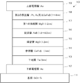
- the MTJ element 10 has a structure in which a reference layer 14, a barrier layer 15, a recording layer 16, a first protective layer 17, and a second protective layer 18 are stacked in this order. Is provided.
- the second protective layer 18, the first protective layer 17, the recording layer 16, the barrier layer 15, and the reference layer 14 are arranged in this order from the top. The same applies to the other drawings.
- the reference layer (fixed layer) 14 is composed of a CoFeB layer having a thickness of 1.0 nm, and the magnetization direction is fixed in one direction perpendicular to the interface.
- the barrier layer 15 is composed of an MgO layer having a thickness of about 1 nm.
- the recording layer (free layer) 16 is composed of an FeB layer having a thickness of 1.8 nm, and the direction of magnetization changes in a direction perpendicular to the interface by spin injection writing. Note that the thickness of the recording layer 16 is not limited to 1.8 nm and is preferably 1.8 nm to 4 nm.
- the first protective layer 17 (cap layer) is composed of an MgO layer having a thickness of 1.2 nm.
- the second protective layer (cap layer) 18 is formed to a thickness of 1 nm, and is composed of CoFeB as an amorphous material and Ru and Pt as crystalline materials.
- the second protective layer 18 is formed by sputtering.
- the thickness of the second protective layer 18 is not limited to 1 nm and is preferably in the range of 1 nm to 4 nm.
- the interface between the reference layer 14 and the barrier layer 15 and the interface between the barrier layer 15 and the recording layer 16 constitute a magnetic tunnel junction J.
- the magnetic tunnel junction J has a substantially circular junction surface, and its diameter D is preferably 30 nm or less.
- the interface between the recording layer 16 and the first protective layer 17 also has a substantially circular bonding surface, and its diameter D is preferably 30 nm or less.
- at least one of the interface between the reference layer 14 and the barrier layer 15, the interface between the barrier layer 15 and the recording layer 16, and the interface between the recording layer 16 and the first protective layer 17 is substantially circular with a diameter D of 30 nm or less. You may have a joint surface.
- the bonding surface may not be circular, and in that case, it is preferable that the effective area of the bonding surface is smaller than the area of a circle having a diameter of 30 nm.
- the actual MTJ element 10 includes a substrate 11, a lower electrode layer 12 formed on the substrate 11, and a base layer 13 formed on the lower electrode 12.
- a second protective layer 18 is formed in order from the reference layer 14 on the base layer 13.
- An upper electrode layer 19 is formed on the second protective layer 18.
- the substrate 11 is composed of a Si layer and a SiO 2 layer formed thereon.
- the substrate 11 has a structure including transistors and multilayer wiring layers.
- the lower electrode layer 12 is composed of a conductor layer such as Au.
- the underlayer 13 is composed of a Ta layer having a thickness of about 5 nm.
- the underlayer 13 may be made of a metal material such as Cu, CuN, Au, Ag, Ru, or an alloy thereof.
- the underlayer 13 may have a structure in which a plurality of metal material layers are stacked, for example, a Ta layer / Ru layer / Ta layer structure.
- the underlayer 13 is a layer that forms an underlayer for forming the layer of the MTJ element 10 and has a flat surface.
- the upper electrode layer 19 is composed of a conductive layer such as Au. Further, materials such as Ta, Ti, and compounds thereof are also used.
- the MTJ element 10 having the configuration shown in FIGS. 1 to 3 obtains high interface magnetic anisotropy by using Pt, Ru or CoFeB as the material of the second protective layer 18. This point will be specifically described.
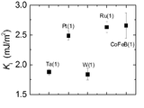
- FIG. 4 shows that the second protective layer 18 is formed with Ta, W, Pt, Ru, CoFeB to a thickness of 1 nm, and the recording layer 16 is formed with FeB to a thickness of 1.8 nm to 4 nm.
- the strength of the interfacial magnetic anisotropy of the joint surface J between the barrier layer 15 and the recording layer 16 of the MTJ element 10 is shown.
- the second protective layer 18 is formed by sputtering, for example, and the subsequent annealing temperature is 300 ° C.
- the value of the interface magnetic anisotropy of the joint surface J is about 1.8 to 1.9 [mJ / m 2 ].
- the interface magnetic anisotropy of the joint surface J is approximately 2.5 [mJ / m 2 ] or more. From this, the interface magnetic anisotropy of the joint surface J of the MTJ element 10 in which the second protective layer 18 is formed of Pt, Ru, or CoFeB is the MTJ in which the second protective layer 18 is formed of Ta or W. It was found that the interface magnetic anisotropy value of the joint surface J of the element 10 was larger.
- the MTJ element 10 of the present embodiment uses Pt, Ru, or CoFeB as the second protective layer 18, and an interface magnetic anisotropy of 2.5 [mJ / m 2 ] or more is obtained.
- a sufficient thermal stability ⁇ can be obtained even in the magnetic tunnel junction surface J having a diameter D of 30 nm or less, for example, a diameter D of about 20 nm. This makes it possible to improve the performance of integrated circuits and memories using magnetic tunnel junctions.
- the reason why the interface magnetic anisotropy is low when a material such as Ta or W is used as the second protective layer 18 is that MgO in which the second protective layer 18 constitutes the first protective layer 17 immediately below. This is to damage the layer.
- the physical cause of damaging the MgO layer is related to the affinity between the substance constituting the second protective layer and oxygen.
- Ta and W have high affinity with oxygen (low energy for generating oxide) and form an oxide that is stable at room temperature. Therefore, when the second protective layer 18 is formed of Ta or W by sputtering, the deposited Ta or W reacts with oxygen in MgO constituting the first protective layer 17 and damages the MgO layer. give.
- Pt, Ru and CoFeB have low affinity with oxygen. For this reason, in the process of forming the second protective layer 18, the deposited Pt, Ru, and CoFeB can form a thin film without damaging the MgO constituting the first protective layer 17.
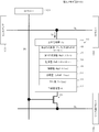
- the magnetic memory circuit 100 has a structure in which the MTJ element 10 and the select transistor 20 are memory cells for 1 bit, and the memory cells are arranged in a matrix.
- the source electrode of the selection transistor 20 is electrically connected to the source line SL, the drain electrode is electrically connected to the lower electrode layer 12 of the MTJ element 10, and the gate electrode is electrically connected to the word line WL. Further, the upper electrode layer 19 of the MTJ element 10 is connected to the bit line BL.
- the word line WL is connected to the X driver (word line driver) 101
- the bit line BL is connected to the Y driver (bit line driver) 102 and the sense amplifier 103
- the source line SL is connected to the source line driver 104. Yes.
- the word line WL, the bit line BL, the source line SL, the X driver 101, the Y driver 102, and the source line driver 104 function as a writing circuit that selects a memory cell (MTJ element 10) and writes data.
- the bit line BL, the source line SL, the X driver 101, the sense amplifier 103, and the source line driver 104 function as a read circuit that selects memory cells and reads stored data.
- the MTJ element 10 has a low resistance.
- the MTJ element 10 has a high resistance when it is antiparallel (parallel and opposite direction: AP state).
- the level of the resistance value is made to correspond to “0” and “1” of the bit information. In this embodiment, “0” is assigned to the low resistance and “1” is assigned to the high resistance.
- the X driver 101 controls the voltage of the word line WL connected to the MTJ element 10 to be written to turn on the corresponding selection transistor 20. Subsequently, the Y driver 102 and the source line driver 104 adjust the voltage applied between the bit line BL connected to the write target MTJ element 10 and the source line SL, and the write current Iw flowing through the MTJ element 10.
- the desired data is written by spin-injection magnetization reversal.
- the magnetization Mr of the recording layer 16 is in the same direction as the magnetization Mf of the reference layer 14, "0" is written, and the write current Iw is changed to the reference layer 14. From the recording layer 16 to the recording layer 16, the magnetization Mr of the recording layer 16 is opposite to the magnetization Mf of the reference layer 14, and “1” is written.
- the X driver 101 applies a selection voltage to the word line WL to turn on the selection transistor 20 connected to the MTJ element 10 to be read, and the Y driver 102 and the source line driver 104 A read voltage is applied between the bit line BL connected to the MTJ element 10 and the source line SL.
- the sense amplifier 103 reads the recorded data by converting this current into a voltage.
- the MTJ element 10 includes the barrier layer 15 between the reference layer 14 and the recording layer 16, the first protective layer 17 on the recording layer 16, and The second protective layer 18 is provided on the first protective layer 17. And since the 2nd protective layer 18 does not damage the 1st protective layer 17, a big magnetic anisotropy is obtained and high thermal stability is obtained.
- the thickness is arbitrary. However, in order to use the perpendicular magnetization due to the interface magnetic anisotropy, the thickness is 5 nm, preferably 3 nm or less, and more preferably 1.6 nm or less. Thereby, the perpendicular magnetization due to the interface magnetic anisotropy becomes the main part of the magnetization of the reference layer 14.
- the material of the reference layer 14 may also contain Co or Fe, and may not contain B. Further, a conventionally known perpendicular magnetic anisotropic material such as FePt or TbTeCo may be used. Furthermore, the reference layer 14 does not need to be a single layer and may be a laminated film. For example, a Co film and Pt film laminate film, a Ni film and Co film laminate film, a multilayer film thereof, a laminate ferrimagnetic structure, or the like can be used as the reference layer 14.
- MgO layer Although a 1.2 nm MgO layer was used as the barrier layer 15, its thickness is preferably 10 nm or less, particularly 5 nm or less.
- the material is not limited to MgO, and other materials such as Al 2 O 3 , SiO 2 , and MgZnO that contain oxygen and generate a magnetic tunnel junction may be used.
- the thickness is arbitrary. However, in order to use the perpendicular magnetization due to the interface magnetic anisotropy, the thickness is 5 nm, preferably 3 nm or less, and more preferably 1.6 nm or less. Thereby, the perpendicular magnetization caused by the interface magnetic anisotropy becomes the main part of the magnetization of the recording layer 16.
- the material of the recording layer 16 is not limited to FeB, and may include at least one of Co, Fe, CoB, FeB, and CoFeB. Furthermore, a trace amount of other elements may be included. Its thickness is also arbitrary. Further, the material of the recording layer 16 may be CoFeBM (where M includes at least one of Ni, Zr, Hf, Ta, Mo, Nb, Pt, Cr, Si, or V).
- the recording layer 16 does not need to be a single layer, and a laminated film can be used as the recording layer 16.
- a laminated film of a layer containing Fe and a layer containing FeB or CoB can be used as the recording layer 16.
- an arrangement configuration of MgO layer (15 or 17), Fe layer, CoFeB layer, MgO layer (17 or 15), an arrangement configuration of MgO layer (15), Fe layer, CoFeB layer, Fe layer, MgO layer (17) Etc. are desirable. This is because in order to obtain high interfacial magnetic anisotropy, it is desirable that B does not exist as much as possible at the interface with MgO.
- the thickness is preferably 5.0 nm or less and 3.0 nm or less.
- the material of the first protective layer 17 may be oxygen other than MgO, and an insulator such as Al 2 O 3 , SiO 2 , MgZnO, Ta 2 O 5 may be used.
- the material of the first protective layer 17 it may be used RuO 2, Vo 2, TiO, Ti 2 O 3, ZnO, conductive oxide such as TaO 2.
- the conductive oxide constituting the first protective layer 17 include RuO 2 , VO 2 , CrO 2 , NbO 2 , MoO 2 , WO 2 , ReO 2 , RhO 2 , OsO 2 , IrO 2 , PtO 2 , Rutile-MoO 2 type oxides such as V 3 O 5 and Ti 3 O 5 may be included.
- the conductive oxide constituting the first protective layer 17 may include NaCl-type oxides such as TiO, VO, NbO, LaO, NdO, SmO, EuO, SrO, BaO, and NiO.
- the conductive oxide film constituting the first protective layer 17 may contain a spinel oxide such as LiTi 2 O 4 , LiV 2 O 4 , Fe 3 O 4 .
- the conductive oxide film constituting the first protective layer 17 is a perovskite such as ReO 3 , CaCrO 3 , SrCrO 3 , BaMoO 3 , SrMoO 3 , CaMoO 3 , LaCuO 3 , CaRuO 3 , SrVO 3 , or BaTiO 3. It may contain —ReO 3 type oxide.
- the conductive oxide layer constituting the first protective layer 17 may contain a corundum oxide such as Ti 2 O 3 , V 2 O 3 , Rh 2 O 3 .
- the conductive oxide layer constituting the first protective layer 17, ZnO, TiO 2, SnO 2 , Cu 2 O, contain Ag 2 O, In 2 O 3 , WO 3 of a is an oxide semiconductor Also good.
- a film containing oxygen can be appropriately selected so that interfacial magnetic anisotropy occurs at the interface with the first protective layer 17.
- the first protective layer 17 is preferably formed to have a thickness equal to or less than that of the barrier layer 15.
- the second protective layer 18 As the second protective layer 18, a 1.0 nm layer of Pt, Ru, CoFeB was used, but its thickness is arbitrary. However, if it is too thick, it becomes difficult to process the magnetic tunnel junction. On the other hand, if it is too thin, the effect cannot be exhibited. Therefore, in the case of Pt and Ru, the thickness of the second protective layer 18 is 3.5 nm or less, preferably 0.3 to 3.0 nm, more preferably 0.5 to 2.0 nm. desirable. In the case of CoFeB, the thickness of the second protective layer 18 is 3.5 nm or less, preferably 0.1 to 3.0 nm, more preferably 0.1 to 1.0 nm.
- the second protective layer 18 does not have to be a single layer and may have a laminated structure.
- a stacked structure of CoFeB, Pt, and Ru, or an alternately stacked structure of Pt and Ru may be used.
- the second protective layer 18 may be a layer containing Co, Fe, CoB, and FeB as a main component in addition to the Pt, Ru, and CoFeB layers. This is because these materials are unlikely to damage MgO constituting the first protective layer 17 disposed adjacent to each other, like Pt and the like.
- the thickness of the second protective layer 18 is 3.5 nm or less, preferably 0.1 to 3.0 nm, more preferably, similarly to the layer containing CoFeB. Is preferably 0.1 to 1.0 nm.
- the layer of Fe, CoFeB, CoB, FeB or the like in the second protective layer 18 functions as a protective layer for the adjacent first protective layer, not as a magnetic layer. Therefore, it is desirable that the second protective layer 18 be formed by adjusting the film thickness or the like so as not to affect the interface magnetic anisotropy value Ki. Therefore, for example, it is desirable to form the second protective layer 18 thinner than the recording layer 16.
- the substrate 11 has a stack of Si layer and the SiO 2 layer, the material and thickness of the substrate is optional.
- Au has been exemplified as the material of the lower electrode layer 12 and the upper electrode layer 19, other arbitrary conductors such as Al can be used.
- the MTJ element 10 including the reference layer 14 and the recording layer 16 made of a ferromagnetic layer is exemplified, but each ferromagnetic layer may be a plurality of layers.
- the recording layer 16 of FIG. 1 has a two-layer structure of recording layers 16A and 16B, and a thin nonmagnetic coupling layer 17B, for example, a Ta layer having a thickness of about 0.1 to 1.0 nm. A layer may be arranged.
- the material for the nonmagnetic coupling layer 17B include Ta, W, Hf, Zr, Nb, Mo, Ti, Mg, and MgO.
- 17A of FIG. 7 is a 1st protective layer.
- the reference layer 14 of FIG. 1 has a two-layer structure of reference layers 14A and 14B, and a thin nonmagnetic coupling layer 15B, for example, a Ta layer having a thickness of about 0.1 to 1.0 nm.
- a layer may be arranged.
- the material for the nonmagnetic coupling layer 15B include Ta, W, Hf, Zr, Nb, Mo, Ti, Mg, MgO, and the like.
- 15A of FIG. 8 is a barrier layer.
- the nonmagnetic coupling layers 17B and 15B may be used for both the recording layers (16A and 16B) and the reference layers (14A and 14B).
- a laminated ferrimagnetic structure can be used as the reference layer 14, and an example thereof is shown in FIG.
- the reference layer 14 has a stacked structure in which a reference layer 14A, a coupling layer 14C, and a reference layer 14B are stacked.
- the reference layers 14A and 14B are made of a ferromagnetic layer.
- the configuration other than the reference layer 14 is the same as that shown in FIG.
- the reference layers 14A and 14B are antiferromagnetically coupled by the coupling layer 14C.
- Ru can be used as the coupling layer 14C.
- the reference layer and the recording layer have a two-layer structure is shown, but a three-layer structure or more may be used.
- the magnetic tunnel junction J illustrated in FIG. 2 is not limited to a circle. It may be oval or square. In this case, as the size of the magnetic tunnel junction, the diameter D of the circular magnetic tunnel junction J having the same effective area may be adopted.
- the invention of the present application can also be applied to an in-plane magnetization type MTJ element as shown in FIG.
- the perpendicular magnetic anisotropy component due to the interfacial magnetic anisotropy is increased, thereby causing spin injection. Tilting the magnetization of the recording layer in the direction perpendicular to the plane during magnetization reversal can be facilitated. Therefore, the efficiency of the spin injection magnetization reversal of the in-plane magnetization MTJ element can be increased.
- the protective layer that increases the thermal stability when the MTJ in the present invention is miniaturized is first found in an MTJ element based on STT magnetization reversal.
- this protective film technique is also effective when the domain wall motion element, the element that modulates the magnetic anisotropy induced by the electric field, and the element that uses the spin orbit torque are miniaturized.
- the second protective layer 18 functions not as a magnetic layer but as a protective layer that protects the adjacent first protective layer 17.
- the second protective layer 18 desirably does not affect the value of the interface magnetic anisotropy, that is, is a nonmagnetic material.
- the second protective layer 18 is made of CoFeB (or Co, Fe, CoB, FeB, etc.)
- the CoFeB is non-magnetic when the film thickness is small, but has magnetization when the film thickness increases. For this reason, it is difficult to keep the second protective layer 18 nonmagnetic when the film thickness is increased.
- a third protective layer made of Ru or the like on the second protective layer 18 is used. It is effective to arrange Hereinafter, the MTJ element 10a having a configuration in which the Ru third protective layer 181 is disposed on the second protective layer 18 will be described.
- the MTJ element 10a includes a third protective layer 181 made of Ru of about 1 nm on the second protective layer 18 made of CoFeB.
- the third protective layer 181 prevents O from desorbing from MgO constituting the first protective layer 17, and further prevents the upper layer material from diffusing into the first protective layer 17. Thus, it is possible to prevent the magnetic characteristics of the MTJ element 10a from deteriorating.
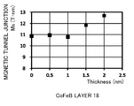
- FIG. 13 shows a relationship between the thickness (0.5 nm to 2.0 nm) of the second protective layer 18 of the MTJ element 10a having the configuration shown in FIG. 12 and the saturation magnetization Ms of the MTJ element 10a.
- the horizontal axis indicates the thickness of the second protective layer 18, and the vertical axis indicates the magnitude [T ⁇ nm] of the saturation magnetization Ms of the MTJ element 10a.
- the saturation magnetization Ms of the MTJ element 10a in which the thickness of the second protective layer 18 is 0 is about 10.9 [T ⁇ nm]. Even if the thickness of the layer 18 is 0.5 and 1.0 nm, the magnitude of the saturation magnetization Ms is substantially the same. On the other hand, when the thickness of the second protective layer 18 is 1.5 nm and 2.0 nm, the magnitude of the saturation magnetization Ms increases as the film thickness increases. That is, the second protective layer 18 is magnetic when the thickness is 1.5 nm or more.
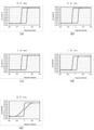
- FIGS. the magnetization curves of the recording layer 16 and the reference layer 14 when a magnetic field is applied perpendicularly to the film surface of each layer to the five MTJ elements 10a including the second protective layers 18 having different thicknesses are shown in FIGS. As shown in FIG.
- FIGS. 14A to 14E show the magnetization curves of the recording layer 16 when the external magnetic field is changed in the range of ⁇ 400 [Oe] to +400 [Oe].
- the horizontal axis indicates the intensity [Oe] of the external magnetic field
- the vertical axis indicates the magnitude [emu / cm 2 ] of magnetization.
- the thickness of the second protective layer 18 when the thickness of the second protective layer 18 is in the range of 0.0 to 1.5 nm, the magnetization curve shows a good square shape.
- FIG. 14E when the thickness of the second protective layer 18 is 2.0 nm, the square shape of the magnetization curve is deteriorated. This indicates that the perpendicular magnetic anisotropy of the MTJ element 10a is mixed with a component of magnetic anisotropy in the plane of the second protective layer 18.
- 15 (a) to 15 (e) show magnetization curves of the reference layer 14 when the external magnetic field is changed in the range of ⁇ 10,000 [Oe] to +10,000 “Oe”.
- the vertical axis represents the magnitude [emu / cm 2 ] of the magnetization, as shown in the figure, when the thickness of the second protective layer 18 is 1.5 nm or less, the external magnetic field is There is a region (plateau region) where the magnetization does not change near 0 [Oe], whereas when the thickness of the second protective layer 18 is 2.0 nm, the external magnetic field is near 0 [Oe]. There is no plateau region, which indicates that the perpendicular magnetic anisotropy is mixed with in-plane magnetic anisotropy components.
- the second protective layer 18 (CoFeB or the like) has a thickness of 0 to 1.5 nm and is nonmagnetic, and the MTJ element 10a exhibits perpendicular magnetic anisotropy.
- the second protective layer 18 is magnetic when the thickness is 1.5 nm.
- the MTJ element 10a still exhibits perpendicular magnetic anisotropy.
- the thickness of the second protective layer 18 exceeds 2.0 nm, an in-plane magnetic film is formed, and the MTJ element 10a cannot obtain perpendicular magnetic anisotropy.
- the second protective layer 18 becomes an in-plane magnetic film
- a large in-plane magnetic field is equivalently applied to the recording layer 16 and the reference layer 14 having an easy axis for perpendicular magnetization due to magnetostatic interaction.
- This in-plane magnetic field deteriorates the thermal stability ⁇ of the recording layer 16.
- the second protective layer 18 when the third protective layer 181 does not exist, the second protective layer 18 has a thickness of about 0.6 nm or more and becomes a magnetic film.
- the second protective layer 18 of the present embodiment is non-magnetic even in the range of 0.6 nm to 1.5 nm may be that the upper Ru diffuses into the second protective layer 18.
- selection of the material of the 3rd protective layer 181 is important, and it is desirable to select the material which maintains the 2nd protective layer 18 nonmagneticly.
- the oxygen composition of the first protective layer 17 needs to be close to stoichiometry, and oxygen from the first protective layer 17 is absorbed. If lost, it becomes difficult to ensure perpendicular magnetization. From this viewpoint, it is desirable that the second protective layer 18 is thick. Therefore, the second protective layer 18 is desirably thick as long as non-magnetic properties are maintained, the thickness is desirably 0.6 to 1.5 nm, and more desirably 0.6 to 1.0 nm.
- the material of the third protective layer 181 is not limited to Ru.
- Ru, Rh, Pd, Cu, Ir, Au, or an alloy thereof as a noble metal material Ta, Hf, W, Zr, Nb, Mo, Ti, as a base metal material, V, Cr, or alloys thereof can be used.
- the material of the third protective layer 181 is Ru, Ti, or Pt
- the characteristics of each MTJ element 10a not provided with the third protective layer 181 are shown in FIGS.
- FIG. 16 shows the magnitude M of the magnetization of the recording layer 16 when an external magnetic field is applied to each MTJ element 10a in the range of ⁇ 10,000 [Oe] to +10,000 [Oe] in the direction perpendicular to each layer. [Emu / cm 2 ] is shown.
- the MTJ element 10a in which the third protective layer 181 is formed of Ru As illustrated, the MTJ element 10a in which the third protective layer 181 is formed of Ru, the MTJ element 10a in which the third protective layer 181 is formed of Ta, the MTJ element in which the third protective layer 181 is not provided, the third The magnitude M of the magnetization increases in the order of the MTJ element 10a in which the protective layer 181 is formed of Pt.
- the magnitude M of the magnetization changes steeply near the zero magnetic field. This indicates that CoFeB constituting the second protective layer 18 has in-plane magnetization.
- the perpendicular magnetic anisotropy Keff ⁇ t [mJ / m 2 ] has a large value when the third protective layer 181 is formed of Ru and Ta.
- the third protective layer 181 is formed of Pt
- the perpendicular magnetic anisotropy Keff ⁇ t becomes slightly larger than when the third protective layer 181 is not disposed. This is because even if Pt diffuses into the second protective film 18, the effect of reducing the magnetization is small, and the magnetization of the second protective film 18 harms the perpendicular magnetization anisotropy of the recording layer 16. Because.
- the second protective layer 18 formed of CoFeB has magnetization, and the in-plane magnetization of the recording layer 17 is large as shown in FIG. Keff: effective magnetic anisotropy energy density, t: thickness of the recording layer 16.
- the second protective layer 18 made of a magnetic layer such as a CoFeB layer and the non-magnetic layer formed thereon are formed.
- the MTJ element 10b including the coupling layer 21 and the ferromagnetic layer 22 formed thereon and having an in-plane magnetization opposite to the second protective layer 18 may be used.
- the second protective layer 18 has a thickness of 0.1 to 3.5 nm, preferably 0.6 to 3.5 nm, for example.
- the coupling layer 21 is preferably made of a material that generates a large interlayer coupling magnetic field such as Ru, Cr, or Ir.
- antiferromagnetic coupling works between the two ferromagnetic layers having an in-plane easy magnetization axis due to magnetostatic interaction. For this reason, the same effect can be obtained by using any material as long as it is a non-magnetic material.
- the ferromagnetic layer 22 can be made of any material such as Co, Fe, CoB, FeB, CoFeB, etc., like the reference layer 14 and the recording layer 16.
- the film thickness of the coupling layer 21 is preferably adjusted as appropriate so as to generate antiferromagnetic interlayer coupling between the second protective layer 18 and the ferromagnetic layer 22.
- the ferromagnetic layer 22 needs to be thicker than the second protective film 18 when using the same or smaller material as the magnetization of the CoFeB layer constituting the second protective film 18.
- the film thickness is appropriately adjusted so that the leakage magnetic field in the in-plane direction is adjusted as small as possible.
- the second protective layer 18 is a magnetic layer and has an easy axis of magnetization in the direction perpendicular to the plane, in the state where the magnetization direction of the recording layer 16 is opposite to the magnetization direction of the second protective layer 18, the MTJ The operation of the element 10 becomes unstable, and the state in the same direction becomes stable. This increases the asymmetry between the information retention time and the magnetization reversal current.
- a coupling layer 21 composed of a nonmagnetic layer is laminated on the second protective layer 18, and further a second layer is formed thereon. It is effective to stack a perpendicular magnetization ferromagnetic layer 22 having a magnetization direction opposite to the magnetization direction of the protective layer 18.
- the ferromagnetic coupling is stabilized by magnetostatic interaction. This ferromagnetic coupling increases as the size of the MTJ element 10b decreases.
- the coupling layer 21 is made of Ru, Cr, Ir, and a material containing them, which generate a large antiferromagnetic coupling between the second protective layer 18 and the ferromagnetic layer 22 thereon. It is desirable to form. The thickness of the coupling layer 21 is appropriately adjusted so that the antiferromagnetic coupling between the second protective layer 18 and the ferromagnetic layer 22 is increased.
- materials having perpendicular magnetization materials such as Co, CoPt alloy, CoPd alloy, FePt alloy, FePd alloy, CoFeB, and FeB are used.
- Ferrimagnetic materials such as TbFeCo are also candidates.
- the coupling layer 21 and the ferromagnetic layer 22 are independent of the thickness of the second protective layer 18 and regardless of whether the second protective layer 18 is a magnetic layer or a nonmagnetic layer. It may be arranged.
- a third protective layer 181 made of Ru or the like is disposed on the second protective layer 18 made of CoFeB or the like.
- the second protective layer 18 is a nonmagnetic film even at 0.6 to 1.0 nm, and does not affect the perpendicular magnetic anisotropy of the MTJ element 10a even at 1.5 nm. Therefore, the present invention is completely different from the technique of the above document.
- Embodiment 3 of the present application when the second protective layer 18 is an in-plane magnetic layer, the nonmagnetic layer 21 and the ferromagnetic layer 22 are stacked on the second protective layer 18, and the second The magnetization direction of the protective layer 18 is opposite to the magnetization direction of the ferromagnetic layer 22. Thereby, the influence of the magnetization of the second protective layer 18 on the perpendicular magnetic anisotropy of the reference layer 14 and the recording layer 16 is reduced.
- the above document does not disclose such a technique at all. Therefore, the present invention is completely different from the technique of the above document.
Landscapes
- Engineering & Computer Science (AREA)
- Computer Hardware Design (AREA)
- Mram Or Spin Memory Techniques (AREA)
- Hall/Mr Elements (AREA)
Abstract
Description
強磁性体から構成される参照層と、
Oを含む障壁層と、
Co又はFeを含む強磁性体から構成される記録層と、
Oを含む第1の保護層と、
Pt、Ru、Co、Fe、CoB、FeB又はCoFeBの少なくとも1つを含む第2の保護層と、
が積層して構成されている。
上述の記載の磁気トンネル接合素子から構成された記憶セルと、
前記記憶セルを選択してデータを書き込む書き込み回路と、
前記記憶セルを選択してデータを読み出す読み出し回路と、
を備える。
本実施形態に係る磁気トンネル接合素子(MTJ(Magnetic tunnel junction)素子)10は、高い界面磁気異方性を示す磁気トンネル接合を有する。MTJ素子10は、図1に示すように、参照層14と、障壁層15と、記録層16と、第1の保護層17と、第2の保護層18とがこの順番で積層された構造を備える。なお、図1では上から第2の保護層18、第1の保護層17、記録層16、障壁層15、参照層14の順番となっているが、上下逆でも構わない。他の図面についても同様である。
あるいは、参照層14と障壁層15との界面、障壁層15と記録層16との界面、記録層16と第1の保護層17との界面の少なくとも1つが直径Dが30nm以下のほぼ円形の接合面を有していてもよい。接合面は円形でなくてもよく、その場合は接合面の実効的な面積が直径30nmの円の面積よりも小さい方が好ましい。
下部電極層12は、Au等の導体の層から構成される。
下地層13は、厚さ5nm程度のTaの層から構成される。下地層13は、Cu、CuN、Au、Ag、Ruなどの金属材料、それらの合金などから構成されてもよい。下地層13は、複数の金属材料の層を積層した構造、例えばTa層/Ru層/Ta層といった構造であってもよい。下地層13は、MTJ素子10の層を形成する下地となる層であり、表面が平坦に形成されている。
このことから、第2の保護層18がPt、Ru又はCoFeBで形成されたMTJ素子10の接合面Jの界面磁気異方性は、第2の保護層18がTa又はWで形成されたMTJ素子10の接合面Jの界面磁気異方性の値よりも大きい、ことが判明した。
さらに、参照層14は、単層である必要はなく、積層膜でもよい。例えば、Co膜とPt膜の積層膜、Ni膜とCo膜の積層膜、さらにそれらの多層膜、積層フェリ構造等を参照層14として使用することも可能である。
さらに、記録層16の材質は、CoFeBM(ここでMはNi,Zr,Hf,Ta,Mo,Nb,Pt,Cr,Si又はVを少なくとも1つ含む)などを利用できる。
また、第1の保護層17の膜厚は、障壁層15の膜厚以下に形成されることが望ましい。
段落0068に記載したように、第2の保護層18は、磁性層としてではなく隣接する第1の保護層17を保護する保護層として機能する。また、第2の保護層18は、界面磁気異方性の値には影響を与えないこと、即ち、非磁性体であることが望ましい。
第2の保護層18が磁性層で且つ面内方向に磁化容易軸がある場合、静磁気的な相互作用により、垂直磁化容易性を有する記録層16に大きな面内磁界が印加される。印加された面内磁界は、記録層16の熱安定性Δを劣化させ、MTJ素子の性能を劣化させる。
なお、結合層21には、Ru、Cr、Irといった大きな層間結合磁界を発生させる材料が好適である。ただし、面内磁化容易軸を有する2つの強磁性層の間には、静磁気的な相互作用により、反強磁性結合が働く。このため、非磁性材料であればどのような材料を用いても同様の効果が得られる。また、強磁性層22は、参照層14、記録層16等と同様に、Co、Fe、CoB、FeB、CoFeB等の任意の材料を使用可能である。
11 基板
12 下部電極層
13 下地層
14、14A,14B 参照層(固定層)
15、15A 障壁層(絶縁層)
15B、17B 非磁性結合層
16、16A,16B 記録層(自由層)
17、17A 第1の保護層(絶縁層)
18 第2の保護層(キャップ層)
19 上部電極層
20 選択トランジスタ
21 非磁性層
22 強磁性層
100 磁気メモリ回路
101 Xドライバ
102 Yドライバ
103 センスアンプ
104 ソース線ドライバ
WL ワード線
BL ビット線
SL ソース線
Claims (13)
- 強磁性体から構成される参照層と、
Oを含む障壁層と、
Co又はFeを含む強磁性体から構成される記録層と、
Oを含む第1の保護層と、
Pt、Ru、Co、Fe、CoB、FeB又はCoFeBの少なくとも1つを含む第2の保護層と、
が積層して構成された磁気トンネル接合素子。 - 前記第2の保護層は、Pt又はRuを少なくとも1つ含む層から構成され、0.3~3.5nmの厚さを有する、
ことを特徴とする請求項1に記載の磁気トンネル接合素子。 - 前記第2の保護層は、Co、Fe、CoB、FeB又はCoFeBを少なくとも1つを含む層から構成され、0.1~3.5nmの厚さを有する、
ことを特徴とする請求項1に記載の磁気トンネル接合素子。 - 前記参照層と前記障壁層との接合面、前記障壁層と前記記録層との接合面、前記記録層と前記第1の保護層との接合面、の少なくとも1つは、直径30nmの円の面積よりも小さな接合面である、
ことを特徴とする請求項1乃至3の何れか1項に記載の磁気トンネル接合素子。 - 前記記録層は、接触している障壁層又は第1の保護層との界面の磁気異方性に起因して、磁化の方向が界面に垂直である、
ことを特徴とする請求項1乃至4の何れか1項に記載の磁気トンネル接合素子。 - 前記第2の保護層の上に、Ru、Rh、Pd、Cu、Ir、Au、Ta、Hf、W、Zr、Nb、Mo、Ti、V、Cr又はこれらの合金を含む第3の保護層を備える、
ことを特徴とする請求項3に記載の磁気トンネル接合素子。 - 前記第2の保護層は0.6~1.5nmの厚さを有する、
ことを特徴とする請求項6に記載の磁気トンネル接合素子。 - 前記第2の保護層は0.6~1.0nmの厚さを有する、
ことを特徴とする請求項7に記載の磁気トンネル接合素子。 - 前記第2の保護層は非磁性体である、
ことを特徴とする請求項7又は8に記載の磁気トンネル接合素子。 - 前記第2の保護層は磁性を有し、
前記第2の保護層の上に形成された非磁性層と、前記非磁性層の上に形成され、前記第2の保護層の磁化の方向と平行で反対方向に磁化された強磁性層と、をさらに備える、
ことを特徴とする請求項3に記載の磁気トンネル接合素子。 - 前記第2の保護層は0.6~3.5nmの厚さを有する、
ことを特徴とする請求項10に記載の磁気トンネル接合素子。 - 前記強磁性層は、Co、Fe、CoB、FeB、CoFeB、CoPt合金、CoPd合金、FePt合金、FePd合金、フェリ磁性体の少なくとも1つを含む、
ことを特徴とする請求項10又は11に記載の磁気トンネル接合素子。 - 請求項1乃至12の何れか1項に記載の磁気トンネル接合素子から構成された記憶セルと、
前記記憶セルを選択してデータを書き込む書き込み回路と、
前記記憶セルを選択してデータを読み出す読み出し回路と、
を備える磁気メモリ。
Priority Applications (3)
| Application Number | Priority Date | Filing Date | Title |
|---|---|---|---|
| US15/776,902 US11563169B2 (en) | 2015-11-18 | 2016-11-18 | Magnetic tunnel junction element and magnetic memory |
| JP2017551969A JP6806375B2 (ja) | 2015-11-18 | 2016-11-18 | 磁気トンネル接合素子及び磁気メモリ |
| KR1020187016407A KR102736375B1 (ko) | 2015-11-18 | 2016-11-18 | 자기 터널 접합 소자 및 자기 메모리 |
Applications Claiming Priority (2)
| Application Number | Priority Date | Filing Date | Title |
|---|---|---|---|
| JP2015-225994 | 2015-11-18 | ||
| JP2015225994 | 2015-11-18 |
Publications (1)
| Publication Number | Publication Date |
|---|---|
| WO2017086481A1 true WO2017086481A1 (ja) | 2017-05-26 |
Family
ID=58718105
Family Applications (1)
| Application Number | Title | Priority Date | Filing Date |
|---|---|---|---|
| PCT/JP2016/084372 Ceased WO2017086481A1 (ja) | 2015-11-18 | 2016-11-18 | 磁気トンネル接合素子及び磁気メモリ |
Country Status (4)
| Country | Link |
|---|---|
| US (1) | US11563169B2 (ja) |
| JP (1) | JP6806375B2 (ja) |
| KR (1) | KR102736375B1 (ja) |
| WO (1) | WO2017086481A1 (ja) |
Cited By (10)
| Publication number | Priority date | Publication date | Assignee | Title |
|---|---|---|---|---|
| WO2020026637A1 (ja) * | 2018-08-02 | 2020-02-06 | 国立大学法人東北大学 | 磁気抵抗効果素子及び磁気メモリ |
| KR20200022516A (ko) * | 2017-07-21 | 2020-03-03 | 어플라이드 머티어리얼스, 인코포레이티드 | 고온 열 처리에 적합한 자기 터널 접합들 |
| JPWO2019230341A1 (ja) * | 2018-05-31 | 2020-07-09 | Tdk株式会社 | スピン軌道トルク型磁化回転素子、スピン軌道トルク型磁気抵抗効果素子及び磁気メモリ |
| JP2020174141A (ja) * | 2019-04-11 | 2020-10-22 | 国立大学法人東北大学 | 磁気抵抗効果素子及び磁気メモリ |
| US20210057641A1 (en) * | 2018-03-30 | 2021-02-25 | Tohoku University | Magnetic tunnel junction device, method for manufacturing magnetic tunnel junction device, and magnetic memory |
| JPWO2020008853A1 (ja) * | 2018-07-04 | 2021-08-02 | ソニーセミコンダクタソリューションズ株式会社 | 磁気トンネル接合素子及び半導体装置 |
| WO2021251003A1 (ja) * | 2020-06-10 | 2021-12-16 | ソニーセミコンダクタソリューションズ株式会社 | 磁気抵抗効果素子、半導体装置及び電子機器 |
| WO2023063198A1 (ja) * | 2021-10-15 | 2023-04-20 | ソニーセミコンダクタソリューションズ株式会社 | 記憶素子及び記憶装置 |
| WO2023228389A1 (ja) * | 2022-05-26 | 2023-11-30 | Tdk株式会社 | 磁気抵抗効果素子及び磁気抵抗効果素子の製造方法 |
| WO2025197974A1 (ja) * | 2024-03-22 | 2025-09-25 | 国立大学法人東北大学 | 垂直磁化膜、垂直磁化磁気抵抗効果素子 |
Families Citing this family (7)
| Publication number | Priority date | Publication date | Assignee | Title |
|---|---|---|---|---|
| US11770981B2 (en) * | 2018-03-30 | 2023-09-26 | Tohoku University | Magnetoresistive element and magnetic memory |
| WO2020045655A1 (ja) * | 2018-08-30 | 2020-03-05 | 国立大学法人東北大学 | 磁気抵抗効果素子、磁気メモリ、及び、該磁気抵抗効果素子の成膜方法 |
| US12108684B2 (en) * | 2019-07-21 | 2024-10-01 | HeFeChip Corporation Limited | Magnetic tunneling junction element with a composite capping layer and magnetoresistive random access memory device using the same |
| CN113013325B (zh) * | 2019-12-19 | 2023-04-07 | 上海磁宇信息科技有限公司 | 具漏磁场平衡层的磁性隧道结单元及磁性随机存储器 |
| US11251360B2 (en) * | 2020-02-06 | 2022-02-15 | International Business Machines Corporation | MTJ capping layer structure for improved write error rate slopes and thermal stability |
| KR102931786B1 (ko) * | 2020-07-28 | 2026-02-25 | 삼성전자주식회사 | 자기 메모리 소자 |
| US20230317729A1 (en) * | 2022-03-31 | 2023-10-05 | Intel Corporation | Vertical bit data paths for integrated circuits |
Citations (9)
| Publication number | Priority date | Publication date | Assignee | Title |
|---|---|---|---|---|
| JP2008028362A (ja) * | 2006-06-22 | 2008-02-07 | Toshiba Corp | 磁気抵抗素子及び磁気メモリ |
| JP2008103728A (ja) * | 2006-10-17 | 2008-05-01 | Magic Technologies Inc | 磁気トンネル接合素子およびその製造方法 |
| JP2012235015A (ja) * | 2011-05-06 | 2012-11-29 | Sony Corp | 記憶素子及び記憶装置 |
| JP2012238631A (ja) * | 2011-05-10 | 2012-12-06 | Sony Corp | 記憶素子、記憶装置 |
| JP2012244031A (ja) * | 2011-05-23 | 2012-12-10 | Sony Corp | 記憶素子、記憶装置 |
| JP2013115401A (ja) * | 2011-12-01 | 2013-06-10 | Sony Corp | 記憶素子、記憶装置 |
| JP2015088520A (ja) * | 2013-10-28 | 2015-05-07 | ソニー株式会社 | 記憶素子、記憶装置、磁気ヘッド |
| US9337415B1 (en) * | 2015-03-20 | 2016-05-10 | HGST Netherlands B.V. | Perpendicular spin transfer torque (STT) memory cell with double MgO interface and CoFeB layer for enhancement of perpendicular magnetic anisotropy |
| US20160155931A1 (en) * | 2014-12-02 | 2016-06-02 | Qualcomm Incorporated | Magnetic etch stop layer for spin-transfer torque magnetoresistive random access memory magnetic tunnel junction device |
Family Cites Families (32)
| Publication number | Priority date | Publication date | Assignee | Title |
|---|---|---|---|---|
| EP1478936A1 (en) * | 2002-02-25 | 2004-11-24 | Fujitsu Limited | Magnetoresistive spin-valve sensor and magnetic storage apparatus |
| JP4237171B2 (ja) * | 2005-09-14 | 2009-03-11 | Tdk株式会社 | 磁気抵抗効果素子および薄膜磁気ヘッド |
| US7508042B2 (en) | 2006-12-22 | 2009-03-24 | Magic Technologies, Inc. | Spin transfer MRAM device with magnetic biasing |
| US7696551B2 (en) | 2007-09-20 | 2010-04-13 | Magic Technologies, Inc. | Composite hard mask for the etching of nanometer size magnetic multilayer based device |
| FR2931011B1 (fr) | 2008-05-06 | 2010-05-28 | Commissariat Energie Atomique | Element magnetique a ecriture assistee thermiquement |
| JP5117421B2 (ja) * | 2009-02-12 | 2013-01-16 | 株式会社東芝 | 磁気抵抗効果素子及びその製造方法 |
| JP4908540B2 (ja) | 2009-03-25 | 2012-04-04 | 株式会社東芝 | スピンmosfetおよびリコンフィギャラブルロジック回路 |
| US7936598B2 (en) | 2009-04-28 | 2011-05-03 | Seagate Technology | Magnetic stack having assist layer |
| FR2963153B1 (fr) | 2010-07-26 | 2013-04-26 | Centre Nat Rech Scient | Element magnetique inscriptible |
| US8722543B2 (en) | 2010-07-30 | 2014-05-13 | Headway Technologies, Inc. | Composite hard mask with upper sacrificial dielectric layer for the patterning and etching of nanometer size MRAM devices |
| US9082951B2 (en) * | 2011-02-16 | 2015-07-14 | Avalanche Technology, Inc. | Magnetic random access memory with perpendicular enhancement layer |
| FR2966636B1 (fr) | 2010-10-26 | 2012-12-14 | Centre Nat Rech Scient | Element magnetique inscriptible |
| CN103460374B (zh) | 2011-03-22 | 2016-02-10 | 瑞萨电子株式会社 | 磁存储器 |
| JP5655689B2 (ja) | 2011-04-21 | 2015-01-21 | Tdk株式会社 | スピン伝導素子 |
| US9105832B2 (en) | 2011-08-18 | 2015-08-11 | Cornell University | Spin hall effect magnetic apparatus, method and applications |
| JP5809903B2 (ja) * | 2011-09-21 | 2015-11-11 | 株式会社東芝 | 不揮発性記憶装置 |
| US9293694B2 (en) | 2011-11-03 | 2016-03-22 | Ge Yi | Magnetoresistive random access memory cell with independently operating read and write components |
| KR101858308B1 (ko) | 2011-11-08 | 2018-05-15 | 도호쿠 다이가쿠 | 터널 자기 저항 효과 소자 및 그것을 사용한 랜덤 액세스 메모리 |
| JP2013115399A (ja) * | 2011-12-01 | 2013-06-10 | Sony Corp | 記憶素子、記憶装置 |
| US8823118B2 (en) * | 2012-01-05 | 2014-09-02 | Headway Technologies, Inc. | Spin torque transfer magnetic tunnel junction fabricated with a composite tunneling barrier layer |
| CN104704564B (zh) | 2012-08-06 | 2017-05-31 | 康奈尔大学 | 磁性纳米结构中基于自旋霍尔扭矩效应的电栅控式三端子电路及装置 |
| WO2014065049A1 (ja) | 2012-10-25 | 2014-05-01 | 日本電気株式会社 | 磁壁移動型メモリセル及びその初期化処理方法 |
| US9099641B2 (en) | 2012-11-06 | 2015-08-04 | The Regents Of The University Of California | Systems and methods for implementing magnetoelectric junctions having improved read-write characteristics |
| US8981505B2 (en) * | 2013-01-11 | 2015-03-17 | Headway Technologies, Inc. | Mg discontinuous insertion layer for improving MTJ shunt |
| US9093148B2 (en) * | 2013-03-22 | 2015-07-28 | Kabushiki Kaisha Toshiba | Resistance change type memory |
| US9691458B2 (en) | 2013-10-18 | 2017-06-27 | Cornell University | Circuits and devices based on spin hall effect to apply a spin transfer torque with a component perpendicular to the plane of magnetic layers |
| JP6414754B2 (ja) | 2013-11-06 | 2018-10-31 | 日本電気株式会社 | 磁気抵抗効果素子および磁気メモリ |
| CN107004440B (zh) | 2014-07-17 | 2021-04-16 | 康奈尔大学 | 基于用于有效自旋转移矩的增强自旋霍尔效应的电路和装置 |
| KR102080631B1 (ko) * | 2014-08-08 | 2020-02-24 | 고쿠리츠 다이가쿠 호진 도호쿠 다이가쿠 | 자기 저항 효과 소자 및 자기 메모리 장치 |
| US9218864B1 (en) | 2014-10-04 | 2015-12-22 | Ge Yi | Magnetoresistive random access memory cell and 3D memory cell array |
| US9728712B2 (en) | 2015-04-21 | 2017-08-08 | Spin Transfer Technologies, Inc. | Spin transfer torque structure for MRAM devices having a spin current injection capping layer |
| TWI581261B (zh) | 2016-03-15 | 2017-05-01 | 賴志煌 | 自旋軌道扭力式磁性隨存記憶體及其寫入方法 |
-
2016
- 2016-11-18 WO PCT/JP2016/084372 patent/WO2017086481A1/ja not_active Ceased
- 2016-11-18 KR KR1020187016407A patent/KR102736375B1/ko active Active
- 2016-11-18 US US15/776,902 patent/US11563169B2/en active Active
- 2016-11-18 JP JP2017551969A patent/JP6806375B2/ja active Active
Patent Citations (9)
| Publication number | Priority date | Publication date | Assignee | Title |
|---|---|---|---|---|
| JP2008028362A (ja) * | 2006-06-22 | 2008-02-07 | Toshiba Corp | 磁気抵抗素子及び磁気メモリ |
| JP2008103728A (ja) * | 2006-10-17 | 2008-05-01 | Magic Technologies Inc | 磁気トンネル接合素子およびその製造方法 |
| JP2012235015A (ja) * | 2011-05-06 | 2012-11-29 | Sony Corp | 記憶素子及び記憶装置 |
| JP2012238631A (ja) * | 2011-05-10 | 2012-12-06 | Sony Corp | 記憶素子、記憶装置 |
| JP2012244031A (ja) * | 2011-05-23 | 2012-12-10 | Sony Corp | 記憶素子、記憶装置 |
| JP2013115401A (ja) * | 2011-12-01 | 2013-06-10 | Sony Corp | 記憶素子、記憶装置 |
| JP2015088520A (ja) * | 2013-10-28 | 2015-05-07 | ソニー株式会社 | 記憶素子、記憶装置、磁気ヘッド |
| US20160155931A1 (en) * | 2014-12-02 | 2016-06-02 | Qualcomm Incorporated | Magnetic etch stop layer for spin-transfer torque magnetoresistive random access memory magnetic tunnel junction device |
| US9337415B1 (en) * | 2015-03-20 | 2016-05-10 | HGST Netherlands B.V. | Perpendicular spin transfer torque (STT) memory cell with double MgO interface and CoFeB layer for enhancement of perpendicular magnetic anisotropy |
Cited By (21)
| Publication number | Priority date | Publication date | Assignee | Title |
|---|---|---|---|---|
| US11251364B2 (en) | 2017-07-21 | 2022-02-15 | Applied Materials, Inc. | Magnetic tunnel junctions suitable for high temperature thermal processing |
| KR20200022516A (ko) * | 2017-07-21 | 2020-03-03 | 어플라이드 머티어리얼스, 인코포레이티드 | 고온 열 처리에 적합한 자기 터널 접합들 |
| KR102512558B1 (ko) * | 2017-07-21 | 2023-03-21 | 어플라이드 머티어리얼스, 인코포레이티드 | 고온 열 처리에 적합한 자기 터널 접합들 |
| JP2020527865A (ja) * | 2017-07-21 | 2020-09-10 | アプライド マテリアルズ インコーポレイテッドApplied Materials,Incorporated | 高温熱処理に適した磁気トンネル接合 |
| JP7133613B2 (ja) | 2017-07-21 | 2022-09-08 | アプライド マテリアルズ インコーポレイテッド | 高温熱処理に適した磁気トンネル接合 |
| US20210057641A1 (en) * | 2018-03-30 | 2021-02-25 | Tohoku University | Magnetic tunnel junction device, method for manufacturing magnetic tunnel junction device, and magnetic memory |
| US11963458B2 (en) * | 2018-03-30 | 2024-04-16 | Tohoku University | Magnetic tunnel junction device, method for manufacturing magnetic tunnel junction device, and magnetic memory |
| JPWO2019230341A1 (ja) * | 2018-05-31 | 2020-07-09 | Tdk株式会社 | スピン軌道トルク型磁化回転素子、スピン軌道トルク型磁気抵抗効果素子及び磁気メモリ |
| US12022742B2 (en) | 2018-07-04 | 2024-06-25 | Sony Semiconductor Solutions Corporation | Magnetic tunnel junction element and semiconductor device |
| JP7399088B2 (ja) | 2018-07-04 | 2023-12-15 | ソニーセミコンダクタソリューションズ株式会社 | 磁気トンネル接合素子及び半導体装置 |
| JPWO2020008853A1 (ja) * | 2018-07-04 | 2021-08-02 | ソニーセミコンダクタソリューションズ株式会社 | 磁気トンネル接合素子及び半導体装置 |
| JP7255898B2 (ja) | 2018-08-02 | 2023-04-11 | 国立大学法人東北大学 | 磁気抵抗効果素子及び磁気メモリ |
| US11765981B1 (en) | 2018-08-02 | 2023-09-19 | Tohoku University | Magnetoresistance effect element and magnetic memory |
| WO2020026637A1 (ja) * | 2018-08-02 | 2020-02-06 | 国立大学法人東北大学 | 磁気抵抗効果素子及び磁気メモリ |
| JPWO2020026637A1 (ja) * | 2018-08-02 | 2021-08-05 | 国立大学法人東北大学 | 磁気抵抗効果素子及び磁気メモリ |
| JP2020174141A (ja) * | 2019-04-11 | 2020-10-22 | 国立大学法人東北大学 | 磁気抵抗効果素子及び磁気メモリ |
| JP7398770B2 (ja) | 2019-04-11 | 2023-12-15 | 国立大学法人東北大学 | 磁気抵抗効果素子及び磁気メモリ |
| WO2021251003A1 (ja) * | 2020-06-10 | 2021-12-16 | ソニーセミコンダクタソリューションズ株式会社 | 磁気抵抗効果素子、半導体装置及び電子機器 |
| WO2023063198A1 (ja) * | 2021-10-15 | 2023-04-20 | ソニーセミコンダクタソリューションズ株式会社 | 記憶素子及び記憶装置 |
| WO2023228389A1 (ja) * | 2022-05-26 | 2023-11-30 | Tdk株式会社 | 磁気抵抗効果素子及び磁気抵抗効果素子の製造方法 |
| WO2025197974A1 (ja) * | 2024-03-22 | 2025-09-25 | 国立大学法人東北大学 | 垂直磁化膜、垂直磁化磁気抵抗効果素子 |
Also Published As
| Publication number | Publication date |
|---|---|
| JP6806375B2 (ja) | 2021-01-06 |
| US11563169B2 (en) | 2023-01-24 |
| KR20180098248A (ko) | 2018-09-03 |
| JPWO2017086481A1 (ja) | 2018-09-20 |
| KR102736375B1 (ko) | 2024-11-28 |
| US20190019944A1 (en) | 2019-01-17 |
Similar Documents
| Publication | Publication Date | Title |
|---|---|---|
| JP6806375B2 (ja) | 磁気トンネル接合素子及び磁気メモリ | |
| US9153306B2 (en) | Tunnel magnetoresistive effect element and random access memory using same | |
| US10217501B2 (en) | Memory element and memory apparatus | |
| JP6934673B2 (ja) | 磁気トンネル接合素子および磁気メモリ | |
| CN103151454B (zh) | 存储元件和存储设备 | |
| US10439133B2 (en) | Method and system for providing a magnetic junction having a low damping hybrid free layer | |
| US9818932B2 (en) | Storage element, storage device, and magnetic head | |
| JP2009094104A (ja) | 磁気抵抗素子 | |
| JP2017059594A (ja) | 磁気メモリ | |
| CN102800803A (zh) | 存储元件和存储设备 | |
| JP6876335B2 (ja) | 磁気トンネル接合素子およびその製造方法 | |
| CN104662686A (zh) | 存储元件、存储装置和磁头 | |
| JP2013115400A (ja) | 記憶素子、記憶装置 | |
| JP2018157091A (ja) | 磁気抵抗素子及び磁気メモリ | |
| CN103137853A (zh) | 存储元件和存储设备 | |
| WO2023276273A1 (ja) | 磁気メモリ素子及び半導体装置 | |
| KR20220092548A (ko) | 터널 접합 적층막, 자기 메모리 소자 및 자기 메모리 | |
| JP2008153527A (ja) | 記憶素子及びメモリ | |
| CN118829347A (zh) | 合成反铁磁结构、mtj和mram | |
| WO2020026637A1 (ja) | 磁気抵抗効果素子及び磁気メモリ | |
| CN114695645B (zh) | Mtj和存储器 |
Legal Events
| Date | Code | Title | Description |
|---|---|---|---|
| 121 | Ep: the epo has been informed by wipo that ep was designated in this application |
Ref document number: 16866481 Country of ref document: EP Kind code of ref document: A1 |
|
| ENP | Entry into the national phase |
Ref document number: 2017551969 Country of ref document: JP Kind code of ref document: A |
|
| NENP | Non-entry into the national phase |
Ref country code: DE |
|
| ENP | Entry into the national phase |
Ref document number: 20187016407 Country of ref document: KR Kind code of ref document: A |
|
| WWE | Wipo information: entry into national phase |
Ref document number: 1020187016407 Country of ref document: KR |
|
| 122 | Ep: pct application non-entry in european phase |
Ref document number: 16866481 Country of ref document: EP Kind code of ref document: A1 |