WO2014065049A1 - 磁壁移動型メモリセル及びその初期化処理方法 - Google Patents
磁壁移動型メモリセル及びその初期化処理方法 Download PDFInfo
- Publication number
- WO2014065049A1 WO2014065049A1 PCT/JP2013/075395 JP2013075395W WO2014065049A1 WO 2014065049 A1 WO2014065049 A1 WO 2014065049A1 JP 2013075395 W JP2013075395 W JP 2013075395W WO 2014065049 A1 WO2014065049 A1 WO 2014065049A1
- Authority
- WO
- WIPO (PCT)
- Prior art keywords
- domain wall
- region
- current
- memory cell
- wall motion
- Prior art date
Links
Images


Classifications
-
- G—PHYSICS
- G11—INFORMATION STORAGE
- G11C—STATIC STORES
- G11C19/00—Digital stores in which the information is moved stepwise, e.g. shift registers
- G11C19/02—Digital stores in which the information is moved stepwise, e.g. shift registers using magnetic elements
- G11C19/08—Digital stores in which the information is moved stepwise, e.g. shift registers using magnetic elements using thin films in plane structure
- G11C19/0808—Digital stores in which the information is moved stepwise, e.g. shift registers using magnetic elements using thin films in plane structure using magnetic domain propagation
- G11C19/0833—Digital stores in which the information is moved stepwise, e.g. shift registers using magnetic elements using thin films in plane structure using magnetic domain propagation using magnetic domain interaction
-
- G—PHYSICS
- G11—INFORMATION STORAGE
- G11C—STATIC STORES
- G11C11/00—Digital stores characterised by the use of particular electric or magnetic storage elements; Storage elements therefor
- G11C11/02—Digital stores characterised by the use of particular electric or magnetic storage elements; Storage elements therefor using magnetic elements
- G11C11/16—Digital stores characterised by the use of particular electric or magnetic storage elements; Storage elements therefor using magnetic elements using elements in which the storage effect is based on magnetic spin effect
- G11C11/161—Digital stores characterised by the use of particular electric or magnetic storage elements; Storage elements therefor using magnetic elements using elements in which the storage effect is based on magnetic spin effect details concerning the memory cell structure, e.g. the layers of the ferromagnetic memory cell
-
- G—PHYSICS
- G11—INFORMATION STORAGE
- G11C—STATIC STORES
- G11C11/00—Digital stores characterised by the use of particular electric or magnetic storage elements; Storage elements therefor
- G11C11/02—Digital stores characterised by the use of particular electric or magnetic storage elements; Storage elements therefor using magnetic elements
- G11C11/16—Digital stores characterised by the use of particular electric or magnetic storage elements; Storage elements therefor using magnetic elements using elements in which the storage effect is based on magnetic spin effect
- G11C11/165—Auxiliary circuits
- G11C11/1675—Writing or programming circuits or methods
-
- G—PHYSICS
- G11—INFORMATION STORAGE
- G11C—STATIC STORES
- G11C11/00—Digital stores characterised by the use of particular electric or magnetic storage elements; Storage elements therefor
- G11C11/02—Digital stores characterised by the use of particular electric or magnetic storage elements; Storage elements therefor using magnetic elements
- G11C11/16—Digital stores characterised by the use of particular electric or magnetic storage elements; Storage elements therefor using magnetic elements using elements in which the storage effect is based on magnetic spin effect
- G11C11/165—Auxiliary circuits
- G11C11/1677—Verifying circuits or methods
-
- G—PHYSICS
- G11—INFORMATION STORAGE
- G11C—STATIC STORES
- G11C11/00—Digital stores characterised by the use of particular electric or magnetic storage elements; Storage elements therefor
- G11C11/02—Digital stores characterised by the use of particular electric or magnetic storage elements; Storage elements therefor using magnetic elements
- G11C11/16—Digital stores characterised by the use of particular electric or magnetic storage elements; Storage elements therefor using magnetic elements using elements in which the storage effect is based on magnetic spin effect
- G11C11/165—Auxiliary circuits
- G11C11/1697—Power supply circuits
-
- G—PHYSICS
- G11—INFORMATION STORAGE
- G11C—STATIC STORES
- G11C11/00—Digital stores characterised by the use of particular electric or magnetic storage elements; Storage elements therefor
- G11C11/18—Digital stores characterised by the use of particular electric or magnetic storage elements; Storage elements therefor using Hall-effect devices
-
- H—ELECTRICITY
- H10—SEMICONDUCTOR DEVICES; ELECTRIC SOLID-STATE DEVICES NOT OTHERWISE PROVIDED FOR
- H10N—ELECTRIC SOLID-STATE DEVICES NOT OTHERWISE PROVIDED FOR
- H10N50/00—Galvanomagnetic devices
- H10N50/10—Magnetoresistive devices
-
- H—ELECTRICITY
- H10—SEMICONDUCTOR DEVICES; ELECTRIC SOLID-STATE DEVICES NOT OTHERWISE PROVIDED FOR
- H10N—ELECTRIC SOLID-STATE DEVICES NOT OTHERWISE PROVIDED FOR
- H10N50/00—Galvanomagnetic devices
- H10N50/80—Constructional details
Definitions
- the present invention relates to a domain wall motion type memory cell and an initialization processing method thereof.
- Magnetic random access memory is a memory that stores information in the direction of magnetization of a magnetic layer. MRAM is being developed because it has desirable features such as low voltage operation, non-volatility, infinite number of rewrites in principle, and high-speed operation.
- MRAM Magnetic random access memory
- a domain wall motion type MRAM that induces and controls the magnetization reversal of the recording layer with a torque that acts between the spin of electrons and the magnetic moment localized in the magnetic material. This magnetization reversal is hereinafter referred to as “current driven domain wall motion”.
- the domain wall motion type MRAM is described in Patent Documents 1 to 5, for example.
- a domain wall motion type MRAM uses a domain wall motion element as a memory element.
- the domain wall motion element includes a recording layer 10 in which the domain wall MW moves, and a magnetic layer (first and second fixed layers 16 and 17) that is magnetically coupled to the magnetization of the recording layer 10.
- the recording layer 10 includes an inversion region 13 in which the magnetization direction can be reversed, and two fixed regions (first and second fixed regions 11 and 12) formed on both sides of the inversion region 13.
- the magnetization directions of the first and second fixed regions 11 and 12 are fixed in opposite directions.
- a domain wall MW is formed at the boundary between any one of the fixed areas and the inversion area 13.
- a reading mechanism for reading the magnetization direction of the inversion region 13 is omitted.
- the magnetization direction of the inversion region 13, that is, the position of the domain wall MW is associated with stored data.
- the rewriting of the stored data is performed by moving the domain wall MW to reverse the magnetization direction of the switching region 13.
- a write current is supplied in the in-plane direction in the recording layer 10.
- the domain wall MW moves in the recording layer 10 in accordance with the direction of the conduction electrons that carry the write current.
- Non-Patent Document 1 when a perpendicular magnetization film having perpendicular magnetic anisotropy is used as a magnetization recording layer, the write current is compared with the case of an in-plane magnetization film having in-plane magnetic anisotropy. Has been theoretically suggested to be reduced. Therefore, in the domain wall motion type MRAM, it is preferable to use the perpendicular magnetization film as the magnetization recording layer (domain wall motion layer).
- Non-Patent Documents 2 and 3 a new method for controlling the magnetization of a magnetic film by applying a current to the magnetic film while applying an in-plane magnetic field has been reported in recent years.
- This method has an advantage that a magnetic layer for polarizing electrons is unnecessary and the structure is simple.
- This magnetization reversal phenomenon is thought to be either a Rashba field due to an asymmetric three-layer structure consisting of a heavy metal layer, a ferromagnetic layer, or a metal oxide layer, or spin current injection due to the spin Hall effect of the heavy metal layer.
- this magnetization reversal is referred to as “magnetization reversal induced by an in-plane magnetic field and an in-plane current”.
- the direction in which the magnetization is finally directed depends on the type of heavy metal layer and the order of stacking due to “magnetization reversal induced by in-plane magnetic field and in-plane current”. More specifically, when the ferromagnetic layer is laminated on a heavy metal layer such as Pt, the unity Z in the Z direction, the in-plane magnetic field H, and the in-plane current I are respectively used as vectors, and finally the magnetization is directed to ZXIXH.
- X represents an outer product.
- the magnetization is finally directed in the direction of -ZXIXH.
- the magnetization is finally directed in the direction of -ZXIXH.
- the ferromagnetic layer is laminated under the heavy metal layer such as Ta, the magnetization is finally directed in the ZXIXH direction.
- a heavy metal layer such as Pt
- One role of the fixed layer of the conventional domain wall motion type MRAM is to form (introduce) the domain wall in the recording layer. Forming (introducing) a domain wall in the recording layer is hereinafter referred to as “initialization”.
- a typical domain wall motion type MRAM has a fixed layer having a different holding force stacked on each of two fixed regions in the recording layer. In this case, by applying a uniform external magnetic field having an appropriate strength, only the magnetization direction of one fixed layer and the fixed region can be reversed, and the magnetization direction of the other fixed layer and fixed region can be maintained. That is, the magnetization directions of the two fixed regions can be reversed.
- the fixed layer is one of the important elements for initializing the domain wall motion element.
- the domain wall motion element provided with the fixed layer has a problem that the manufacturing process of the fixed layer is complicated. For example, when the fixed layer is processed, there is a concern that damage due to etching or the like enters the recording layer, so that the magnetic characteristics of the recording layer change and desired magnetic characteristics cannot be obtained. Further, in the domain wall motion element including the fixed layer, there is a concern that the leakage magnetic field from the fixed layer increases the write current value. Therefore, the present invention intends to provide a technique capable of eliminating the need for a fixed layer for initialization in a domain wall motion type MRAM.
- the recording layer includes a magnetic layer, and the recording layer supplies a magnetization switching region in which magnetization can be reversed and spin-polarized electrons to the magnetization switching region.
- a domain wall motion memory cell characterized in that a first region where magnetization reversal occurs and a second region where magnetization reversal does not occur are formed.
- the recording layer includes a magnetic layer, and the recording layer supplies a magnetization switching region in which magnetization can be reversed and spin-polarized electrons to the magnetization switching region.
- Magnetization reversal in the first direction is induced in the region of the third layer, a third current flowing in a direction parallel to the film surface of the magnetic film, and a third magnetic field in a direction parallel to the film surface of the magnetic film.
- a domain wall motion type memory cell characterized in that a magnetization reversal in a second direction antiparallel to the first direction is induced in a fourth region by a component.
- the domain wall motion type MRAM using the perpendicular magnetization film a fixed layer for initialization can be eliminated, so that the manufacturing process can be simplified and the domain wall motion type MRAM is inexpensive. Can provide.
- FIG. 1A is a plan view showing a configuration of a general domain wall motion element.
- FIG. 1B is a longitudinal sectional view showing a configuration of a general domain wall motion element.
- FIG. 2A is a plan view showing the configuration of the domain wall motion element according to the first embodiment of the present invention.
- FIG. 2B is a longitudinal sectional view showing the configuration of the domain wall motion element according to the first embodiment of the present invention.
- FIG. 3A is a conceptual diagram showing one magnetization state of the domain wall motion element according to the first embodiment of the present invention.
- FIG. 3B is a conceptual diagram showing another magnetization state of the domain wall motion element according to the first embodiment of the present invention.
- FIG. 4A is a conceptual diagram illustrating a data write operation with respect to the domain wall motion element according to the first embodiment of the present invention.
- FIG. 4B is a conceptual diagram illustrating a data write operation with respect to the domain wall motion element according to the first embodiment of the present invention.
- FIG. 5 is a conceptual diagram showing a data read operation for the domain wall motion element according to the first embodiment of the present invention.
- FIG. 6A is a conceptual diagram showing a first step of an initialization process for the domain wall motion element according to the first embodiment of the present invention.
- FIG. 6B is a conceptual diagram showing a second step of the initialization process for the domain wall motion element according to the first embodiment of the present invention.
- FIG. 7A is a plan view showing the configuration of the domain wall motion element according to the second embodiment of the present invention.
- FIG. 7B is a longitudinal sectional view showing the configuration of the domain wall motion element according to the second embodiment of the present invention.
- FIG. 8 is a conceptual diagram showing an initialization process for the domain wall motion element according to the second embodiment of the present invention.
- FIG. 9 is a plan view showing a configuration of a domain wall motion element according to a modification of the second embodiment of the present invention.
- FIG. 10 is a conceptual diagram showing an initialization process for a domain wall motion element according to a modification of the second embodiment of the present invention.
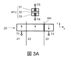
- the domain wall motion element according to the first embodiment includes a recording layer 20 including a reversal region (magnetization reversal region) 23 and first and second fixed regions 21 and 22 on both sides thereof, a sense layer 31, a tunnel barrier layer 32, and a reference.
- a layer 33, a first terminal T1, a second terminal T2, a third terminal T3, and a fourth terminal T4 are provided.
- the + Z direction is defined as a direction perpendicular to the substrate from the back surface to the front surface of the substrate (not shown) as indicated by an arrow z in FIG. 2B.
- the X direction and the Y direction are defined as horizontal directions perpendicular to the Z direction as indicated by arrows x and y in FIG. 2A. Furthermore, the X direction is the longitudinal direction of the domain wall motion element, and the Y direction is defined as a direction perpendicular to the X direction and the Z direction.
- the arrows in the recording layer 20 indicate the magnetization direction of each magnetic layer. In addition, the initial magnetization state is shown as the magnetization state.
- the domain wall motion element according to the first embodiment does not require a fixed layer as compared with the domain wall motion element described with reference to FIGS. 1A and 1B.
- the width (size in the Y direction) of the recording layer 20 is different in each of the inversion region 23, the first fixed region 21, and the second fixed region 22, and is parallel to the film plane in the X direction.
- the current density flowing in each region is different in each region.
- the recording layer 20 is made of a ferromagnetic material. More specifically, the recording layer 20 is formed of a perpendicular magnetization film having perpendicular magnetic anisotropy.
- the material of the recording layer 20 desirably includes at least one selected from Fe, Co, and Ni.
- the recording layer 20 is a thin film having perpendicular magnetic anisotropy such as a Co / Ni laminated film, a Co / Pd laminated film, a Co / Pt laminated film, a Co—Cr—Pt alloy, or a Co—Fe—B alloy. Furthermore, at least one of the upper and lower layers (not shown) of the recording layer 20 is preferably a heavy metal such as Pt, Pd, or Ta. The other of the upper and lower layers (not shown) of the recording layer 20 is preferably a metal oxide such as Mg—O or Al—O.
- the sense layer 31 is made of a ferromagnetic material. More specifically, the sense layer 31 is formed of an in-plane magnetization film having in-plane magnetic anisotropy.
- the material of the sense layer 31 desirably includes at least one selected from Fe, Co, and Ni.
- the sense layer 31 uses a thin film having in-plane magnetic anisotropy, such as a Ni—Fe alloy, a Co—Fe—B alloy, or a Co—Fe alloy.
- the magnetization direction can be changed to either the + Y direction or the -Y direction.
- the reference layer 33 is made of a ferromagnetic material. More specifically, the reference layer 33 is formed of an in-plane magnetization film having in-plane magnetic anisotropy. The material of the reference layer 33 is the same as that of the sense layer 31. Note that the magnetization of the reference layer 33 is fixed and does not change depending on the writing and reading operations. Therefore, for example, an antiferromagnetic layer (not shown) may be stacked on the reference layer 33.
- the reference layer 33 may be a laminated film including a ferromagnetic layer, a nonmagnetic layer, and a ferromagnetic layer.
- the magnetizations of the two ferromagnetic layers of the laminated film may be set to be antiparallel to each other by antiferromagnetic coupling.
- the tunnel barrier layer 32 is a nonmagnetic layer.
- the tunnel barrier layer 32 is preferably formed of an insulating film, and examples of the material include Mg—O, Al—O, Ni—O, and Hf—O.
- the tunnel barrier layer 32 is sandwiched between the sense layer 31 and the reference layer 33, and a magnetic tunnel junction (MTJ) is formed by the sense layer 31, the tunnel barrier layer 32, and the reference layer 33.
- MTJ magnetic tunnel junction
- the tunnel barrier layer may be formed of a nonmagnetic semiconductor or metal material in addition to the above materials.
- the domain wall MW can move inside the recording layer 20.
- the recording layer 20 includes a first fixed area 21, a second fixed area 22, and an inversion area 23.
- the magnetization is held in the + Z direction by the holding force of the recording layer 20, and the magnetization does not change by writing and reading operations.
- the magnetization is held in the ⁇ Z direction by the holding force of the recording layer 20, and the magnetization does not change by writing and reading operations.
- the inversion region 23 is provided between the first fixed region 21 and the second fixed region 22, and the magnetization direction can be changed to either the + Z direction or the -Z direction.
- the first terminal T ⁇ b> 1 is a current terminal connected to the first fixed region 21.
- the second terminal T ⁇ b> 2 is a current terminal connected to the second fixed region 22.
- the third terminal T3 is a current terminal connected to the sense layer 31.
- the fourth terminal T4 is a current terminal connected to the reference layer 33.
- One of the first terminal T1 and the second terminal T2 and one of the third terminal T3 and the fourth terminal T4 may be combined.
- Magneticization state of data “0” and “1” 3A and 3B show two magnetization states that the domain wall motion element according to the first embodiment can take. Each magnetization state is associated with stored data “0” and “1”. As an example, the magnetization direction of the first fixed region 21 is held in the + Z direction.
- the magnetization direction of the second fixed region 22 is held in the ⁇ Z direction.
- the magnetization of the reference layer 33 is fixed in the + Y direction (the direction from the front side to the back side of the drawing).
- the domain wall MW is formed at a position near the boundary between the inversion region 23 and the second fixed region 22.
- the leakage magnetic field from the inversion region 23 has a component in the + Y direction at the position of the sense layer 31, and the magnetization of the sense layer 31 is directed in the + Y direction according to the direction of the leakage magnetic field.
- the magnetizations of the sense layer 31 and the reference layer 33 are parallel, and the resistance value of the MTJ is low (low resistance state).
- This low resistance state is associated with, for example, data “0”.
- FIG. 3B when the magnetization of the inversion region 23 is in the ⁇ Z direction, the domain wall MW is formed at a position near the boundary between the inversion region 23 and the first fixed region 21.
- the leakage magnetic field from the inversion region 23 has a component in the -Y direction at the position of the sense layer 31, and the magnetization of the sense layer 31 is directed in the -Y direction according to the direction of the leakage magnetic field.
- the magnetizations of the sense layer 31 and the reference layer 33 are antiparallel, and the MTJ resistance value is high (high resistance state).
- This high resistance state is associated with, for example, data “1”.
- the domain wall MW existing at a certain position in the recording layer 20 can remain stably at that position unless an external force is applied. This is because there are innumerable pinning sites in the material having perpendicular magnetic anisotropy, and they have sufficient thermal stability.
- (Write operation) 4A and 4B are conceptual diagrams illustrating a write operation of the domain wall motion element according to the first embodiment. For convenience of explanation, illustration of MTJ is omitted. As an example, the magnetization direction of the first fixed region 21 is held in the + Z direction.
- the magnetization direction of the second fixed region 22 is held in the ⁇ Z direction.
- the write current value required for the domain wall MW to move in the inversion region 23 is IW_TH0
- the write current value required for the domain wall MW to move in the first fixed region 21 is IW_TH1
- the domain wall MW moves in the second fixed region 22.
- a write current value necessary for this is IW_TH2.
- FIG. 4A shows the write current IW0 supplied at the time of rewriting from data “1” to data “0”.
- the write current IW0 flows from the terminal T2 through the recording layer 20 to the terminal T1.
- spin-polarized electrons are injected into the inversion region 23 from the first fixed region 21.
- the spin of the injected electrons drives the domain wall MW at the boundary between the first fixed region 21 and the inversion region 23 in the direction of the second fixed region 22.
- the magnitude of the write current IW0 is set larger than the write current IW_TH0 and smaller than the write current IW_TH1.
- the domain wall MW moves to the boundary between the second fixed region 22 and the inversion region 23, and the magnetization direction of the inversion region 23 is inverted in the + Z direction.
- the write current IW1 flows from the terminal T1 through the recording layer 20 to the terminal T2.
- spin-polarized electrons are injected from the second fixed region 22 into the inversion region 23.
- the spin of the injected electrons drives the domain wall MW at the boundary between the second fixed region 22 and the inversion region 23 in the direction of the first fixed region 21.
- the magnitude of the write current IW1 is set larger than the write current IW_TH0 and smaller than the write current IW_TH1.
- FIG. 5 is a conceptual diagram showing a read operation of the domain wall motion element according to the first embodiment. For convenience of explanation, the recording layer is not shown.
- a read current IR is supplied between the terminal T3 and the terminal T4.
- the read current flows through the MTJ so as to penetrate the tunnel barrier layer 32.
- the resistance value of the MTJ is detected, and the magnetization direction of the inversion region is sensed.
- Initialization 6A and 6B are conceptual diagrams showing initialization of the domain wall motion element according to the first embodiment. For convenience of explanation, illustration of MTJ is omitted.
- Initialization of the domain wall motion element of the first embodiment utilizes “magnetization reversal induced by in-plane magnetic field and in-plane current”. Let I_INI_TH0, I_INI_TH1, and I_INI_TH2 be current values at which magnetization reversal occurs in the magnetization reversal region, the first fixed region, and the second fixed region in a certain in-plane magnetic field.
- the widths in the Y direction of the inversion region 23, the first fixed region 21, and the second fixed region 22 are different, the current densities of the respective regions are different. Since the width of the inversion region 23 in the Y direction is the smallest, the write current I_INI_TH0 necessary for the magnetization inversion of the inversion region 23 is the smallest. Next, since the width in the Y direction of the first fixed region 21 is the next smallest, the write current I_INI_TH1 necessary for the magnetization reversal of the first fixed region 21 is the next smallest.
- FIG. 6A shows the first step.
- an external magnetic field in the ⁇ Z direction (third direction) is uniformly applied to the domain wall motion element.
- the magnetization of the inversion region 23, the first fixed region 21, and the second fixed region 22 is ⁇ Turn in the Z direction.
- FIG. 6B shows the second step.
- an external magnetic field (first magnetic field component) in the ⁇ X direction (direction parallel to the film surface of the recording layer) is uniformly applied to the domain wall motion element.
- An initialization current I_INI (first current) supplied at the time of initialization flows from the terminal T1 through the recording layer 20 to the terminal T2.
- the initialization current I_INI is larger than the write current I_INI_TH0 necessary for the magnetization reversal of the inversion region 23, larger than the write current I_INI_TH1 necessary for the magnetization reversal of the first fixed region 21, and the write necessary for the magnetization reversal of the second fixed region 22
- the current is smaller than I_INI_TH2.
- the magnetization of the inversion region 23 and the first fixed region 21 is inverted in the + Z direction due to the phenomenon of “magnetization inversion induced by the in-plane magnetic field and the in-plane current”.
- the first fixed region 21 and the inversion region 23 in which the magnetization reversal occurs may be referred to as a first region
- the second fixed region 22 in which the magnetization inversion does not occur may be referred to as a second region.
- the initialization current I_INI can be designed to be larger than the write currents IW0 and IW1. Therefore, it is possible to design so that “the magnetization reversal induced by the in-plane magnetic field and the in-plane current” does not occur when writing data.
- initialization is executed in two steps or one step. However, it is tested whether a domain wall is actually introduced, and initialization is performed only for a failed element in which a domain wall is not introduced.
- the initialization rate may be increased by applying a current and an in-plane magnetic field. Since initialization processing is assumed to be performed before shipping as a product, even if such a verification test is applied to initialization, the test time before shipping will be long, but magnetic random access after collection will be performed. There is no overhead of memory operating speed.
- the initialization current is larger than the write current, but it is not always necessary to increase the cell transistor size so that the initialization current can flow. Normally, the cell transistor is designed so as to be able to supply the write current.
- the power supply voltage may be increased to supply the initialization current.
- the transistor is likely to be destroyed, but the time for which the high voltage is applied is short only at the time of initialization before shipment, and the transistor can be easily designed not to be destroyed.
- the fixed layer for initialization can be dispensed with. Therefore, the manufacturing process can be simplified, and an inexpensive domain wall motion type MRAM can be provided.
- (Second Embodiment) 7A and 7B are a schematic plan view and a longitudinal sectional view of a domain wall motion element according to the second embodiment of the present invention.
- the domain wall motion element according to the second embodiment is different from the first embodiment only in the planar structure. Therefore, the same constituent elements as those in the first embodiment are denoted by the same reference numerals, and redundant descriptions are omitted as appropriate.
- the second embodiment of the present invention as shown in FIG.
- the first fixed area 41 and a part of the inversion area 43 extend in the X-axis direction, and are second fixed. Other portions of the region 42 and the inversion region 43 extend in the Y-axis direction. Furthermore, the width in the Y-axis direction of the first fixed region 41 and the width in the X-axis direction of the second fixed region 42 are larger than the width in the Y-axis direction of the inversion region 43 extending in the X-axis direction. Further, the width of the first fixed region 41 in the Y-axis direction is almost equal to the width of the second fixed region 42 in the X-axis direction.
- the first and second fixed regions 41 and 42 and the inversion region 43 in the recording layer 40 can be said to have the same film configuration.
- the write current value required for the domain wall MW to move in the inversion region 43 is IW_TH0
- the write current value required for the domain wall MW to move in the first fixed region 41 is IW_TH1
- the domain wall MW is IW_TH2.
- the write current IW_TH0 necessary for domain wall driving is the smallest.
- the write currents IW_TH1 and IW_TH2 necessary for domain wall driving are approximately the same, and the write current It is larger than IW_TH0.
- the write current IW0 supplied at the time of rewriting from data “1” to data “0” and the magnitude of the write IW1 supplied at the time of rewriting from data “0” to data “1” are larger than the write current IW_TH0, and By setting the write currents smaller than the write currents IW_TH1 and IW_TH2, the domain wall motion due to the current can be realized in the inversion region 43.
- I_INI_TH0, I_INI_TH1, and I_INI_TH2 be current values at which magnetization reversal occurs in the magnetization reversal region, the first fixed region, and the second fixed region in a certain in-plane magnetic field.
- I_INI_TH0, I_INI_TH1, and I_INI_TH2 be current values at which magnetization reversal occurs in the magnetization reversal region, the first fixed region, and the second fixed region in a certain in-plane magnetic field.
- the widths perpendicular to the current direction the direction indicated by the arrow line I_INI in FIG. 8
- the density is different.
- the write current I_INI_TH0 necessary for the magnetization inversion of the inversion region 43 is the smallest.
- the write currents I_INI_TH1 and I_INI_TH2 required for the magnetization reversal of the first fixed region 41 are approximately the same.
- I_INI_TH0 Initialization is performed in the following one step. As shown in FIG. 8, the direction of the in-plane magnetic field applied to the domain wall motion element at the time of initialization is ⁇ 135 degrees in the XY plane, with the clockwise direction from the X axis being positive.
- the initialization current I_INI flows in the direction of the first fixed region 41-the inversion region 43-the second fixed region 42.
- the initialization current I_INI is larger than the write current I_INI_TH0 necessary for the magnetization reversal of the inversion region 43, larger than the current I_INI_TH1 necessary for the magnetization reversal of the first fixed region 41, and the current I_INI_TH2 necessary for the magnetization reversal of the second fixed region 42. Greater than.
- the magnetization is finally directed in the direction of ZXIXH using the unit vector Z in the Z direction, the in-plane magnetic field H, and the in-plane current I as vectors.
- X is an outer product.
- the inner product of the initialization currents I_INI (second current) and Hxy (second magnetic field component) is negative in the first fixed region 41 and a part of the inversion region 43 extending in the X-axis direction. Therefore, the magnetization finally faces in the + Z direction.
- the inner product of the initialization currents I_INI (third current) and Hxy (third magnetic field component) is positive in the second fixed region 42 and other regions extending in the Y-axis direction of the inversion region 43. The magnetization finally faces in the -Z direction.
- the domain wall can be introduced into the inversion region 43.
- the magnetization directions of the first fixed region 41 and the second fixed region 42 can be antiparallel to each other.
- magnetization reversal in the first direction is induced in the third region including the first fixed region 41 and the inverted region 43 extended in the X-axis direction, and the inverted region 43 extended in the Y-axis direction and the second fixed region. It can be said that magnetization reversal in a second direction antiparallel to the first direction is induced in the fourth region including the region 42. If the third direction described in the first embodiment is defined in association with the first and second directions, it can be said that the third direction is a direction perpendicular to the first and second directions.
- the initialization current I_INI can be designed to be larger than the write currents IW0 and IW1.
- FIG. 9 is a schematic plan view of a domain wall motion element according to a modification of the second embodiment.
- the domain wall motion element according to the modification of the second embodiment is different from the second embodiment only in the planar structure. Therefore, the same constituent elements as those in the second embodiment are denoted by the same reference numerals, and redundant descriptions are omitted as appropriate.
- the inversion region 53 extends in the X-axis direction
- the first fixed region 51 and the second fixed region 52 extend in the Y-axis direction.
- the width of the first fixed region 51 in the X-axis direction and the width of the second fixed region 52 in the X-axis direction are larger than the width of the inversion region 53 in the Y-axis direction. Further, the width of the first fixed region 51 in the X-axis direction is almost equal to the width of the second fixed region 52 in the X-axis direction.
- the write current value required for the domain wall MW to move in the inversion region 53 is IW_TH0
- the write current value required for the domain wall MW to move in the first fixed region 51 is IW_TH1
- the domain wall MW moves in the second fixed region 52.
- a write current value necessary for this is IW_TH2.
- the write current IW_TH0 necessary for the domain wall drive is the smallest.
- the write currents IW_TH1 and IW_TH2 are about the same and larger than the write current IW_TH0.
- the magnitudes of the write currents IW0 and IW1 are set to be larger than the write current IW_TH0 and smaller than the write currents IW_TH1 and IW_TH2, thereby realizing domain wall movement due to the current in the inversion region 53.
- FIG. 10 is a conceptual diagram illustrating initialization of a domain wall motion element according to a modification of the second embodiment. Initialization is performed in the following one step. The initialization of the domain wall motion element according to this modification uses “magnetization reversal induced by an in-plane magnetic field and an in-plane current”. Let I_INI_TH0, I_INI_TH1, and I_INI_TH2 be current values at which magnetization reversal occurs in the magnetization reversal region, the first fixed region, and the second fixed region in a certain in-plane magnetic field.
- the widths perpendicular to the current direction of the inversion region 53, the first fixed region 51, and the second fixed region 52 are different, the current density of each region is Different. Since the width of the inversion region 53 is the smallest, the write current I_INI_TH0 necessary for the magnetization inversion of the inversion region 53 is the smallest. Next, since the width of the first fixed region 51 and the width of the second fixed region 52 are approximately the same, the write currents I_INI_TH1 and I_INI_TH2 required for the magnetization reversal of the first fixed region 51 are approximately the same, and the write current Next to I_INI_TH0. As shown in FIG.
- the direction of the in-plane magnetic field applied to the domain wall motion element during initialization is the ⁇ Y direction.
- the initialization current I_INI flows in the direction from the first fixed region 51 to the inversion region 53 to the second fixed region 52.
- the initialization current I_INI is larger than the write current I_INI_TH1 necessary for the magnetization reversal of the first fixed region 51 and larger than the write current I_INI_TH2 necessary for the magnetization reversal of the second fixed region 52.
- the magnetization is finally directed in the direction of ZXIXH using the unit vector Z in the Z direction, the in-plane magnetic field H, and the in-plane current I as vectors.
- the magnetization directions of the first fixed region 51 and the second fixed region 52 can be made antiparallel to each other.
- the fixed layer for initialization can be dispensed with in the domain wall motion type MRAM using the perpendicular magnetization film. Therefore, the manufacturing process can be simplified, and an inexpensive domain wall motion type MRAM can be provided.
- the widths of the first fixed region and the second fixed region that are perpendicular to the direction in which the current flows may be approximately the same, so that the initialization current margin can be widened. it can.
- the present invention has been described above with reference to a plurality of embodiments and modifications. However, the present invention is not limited to the above-described embodiments, and each embodiment may be appropriately modified or modified within the scope of the technical idea of the present invention. Obviously, it can be changed.
- the threshold current for writing and initialization is set based on the difference between the widths of the inversion region and the fixed region, but writing and initialization are not only performed based on the width direction but also the thickness direction (Z direction).
- the threshold current may be controlled.
- the thickness of the second fixed region 22 is made larger than that of the first fixed region 21.
- the write threshold current is set by the difference in width between the inversion region and the fixed region, and the domain wall is prevented from entering the fixed region during writing.
- the surface morphology of the base of the fixed region is changed.
- the domain wall may be prevented from entering the fixed region.
- the width or thickness direction may be the same in the fixed region and the reverse region without changing the current density of the reverse region and the fixed region.
- the domain wall is kept thermally stable by utilizing innumerable pinning sites in the material having perpendicular magnetic anisotropy. A step may be provided between the regions.
- the MTJ is provided at a position physically separated from the inversion region.
- a tunnel barrier film is formed in contact with the inversion region, and a reference layer having perpendicular magnetic anisotropy is formed as the tunnel barrier film.
- the magnetization of the switching region may be read out by forming it on the opposite side of the switching region.
- the in-plane magnetic field is applied from the outside.
- a magnetic field generated by providing a wiring near the domain wall motion element and passing a current through the wiring may be used.
- a magnetization reversal induced by an in-plane magnetic field + an in-plane current may be caused only in the first fixed region by providing a wire in the vicinity of the first fixed region and passing a current through the wire. Also, by providing the first wiring in the vicinity of the first fixed region, providing the second wiring in the second fixed region, and controlling the direction of the current flowing through the first wiring and the second wiring, In two fixed regions, the direction of reversal by “in-plane magnetic field + magnetization reversal induced by in-plane current” may be set antiparallel.
- the said embodiment is a memory cell of a magnetic random access memory
- This application claims the priority on the basis of Japanese application Japanese Patent Application No. 2012-235563 for which it applied on October 25, 2012, and takes in those the indications of all here.
Landscapes
- Engineering & Computer Science (AREA)
- Computer Hardware Design (AREA)
- Hall/Mr Elements (AREA)
- Mram Or Spin Memory Techniques (AREA)
Abstract
Description
近年、電子の持つスピンと磁性体に局在している磁気モーメントとの間に働くトルクで記録層の磁化反転を誘起・制御する、磁壁移動型のMRAMが提案されている。この磁化反転は、以下では、「電流駆動磁壁移動」と参照される。磁壁移動型のMRAMは、例えば、特許文献1から5に記載されている。
磁壁移動型のMRAMは、磁壁移動素子を記憶素子として用いる。図1A及び図1Bは、典型的な磁壁移動素子の概略平面図及び断面図である。磁壁移動素子は、磁壁MWが移動する記録層10、及び、記録層10の磁化と磁気的な結合をした磁性層(第1、第2固定層16、17)を備える。記録層10は、磁化方向が反転可能な反転領域13と、その反転領域13の両側に形成された2つの固定領域(第1、第2固定領域11、12)とを備える。第1、第2固定領域11、12のそれぞれの磁化方向は、互いに逆向きに固定される。その結果、記録層10において、いずれかの固定領域と反転領域13との境界に磁壁MWが形成される。尚、図1A及び図1Bでは、反転領域13の磁化の方向を読み出す、読み出し機構を省略している。
磁壁移動素子では、反転領域13の磁化方向、すなわち、磁壁MWの位置が、記憶データに対応付けられる。記憶データの書き換えは、磁壁MWを移動させて反転領域13の磁化方向を反転させることにより行われる。その磁壁移動のために、記録層10において、書き込み電流が面内方向に供給される。その書き込み電流を担う伝導電子の方向に従って、磁壁MWが記録層10中を移動する。
また、非特許文献1によれば、垂直磁気異方性を有する垂直磁化膜が磁化記録層として用いられる場合、面内磁気異方性を有する面内磁化膜の場合と比較して、書き込み電流が低減されることが理論的に示唆されている。従って、磁壁移動型のMRAMにおいて、垂直磁化膜を磁化記録層(磁壁移動層)として用いることが好ましい。
また、非特許文献2、3によれば、近年、面内磁場を印加しつつ、磁性膜に電流を流すことで、磁性膜の磁化を制御する新しい手法が報告されている。この手法は、電子を偏極させるための磁性層が不要であり、構造が単純であるという利点を有する。この磁化の反転現象は、重金属層、強磁性層、酸化金属層からなる非対称な三層構造によるラシュバ場、もしくは、重金属層のスピンホール効果によるスピン流注入のいずれかと考えられ、現在、盛んに議論されている。以下では、この磁化反転は、「面内磁場と面内電流により誘起された磁化反転」と参照される。
尚、「面内磁場と面内電流により誘起された磁化反転」によって、最終的に磁化が向く方向は重金属層の種類や積層の順番に依存する。具体的には、強磁性層がPtなどの重金属層に積層された場合、Z方向の単位ベクトルZ、面内磁場H、面内電流Iをそれぞれベクトルとして、ZXIXHに最終的に磁化が向く。ここで、Xは外積を表す。また、強磁性層がPtなどの重金属層の下に積層された場合は、−ZXIXHの方向に最終的に磁化が向く。また、強磁性層がTaなどの重金属層の上に積層された場合は、−ZXIXHの方向に最終的に磁化が向く。また、強磁性層がTaなどの重金属層の下に積層された場合は、ZXIXHの方向に最終的に磁化が向く。以下の説明では簡単のため、強磁性層がPtなどの重金属層の上に積層された場合について説明するが、適宜変形または変更することが可能である。
初期化を目的として、典型的な磁壁移動型のMRAMは、保持力の異なる固定層を記録層中の2つの固定領域のそれぞれに積層している。この場合、適切な強度の一様外部磁界を印加することによって、一方の固定層及び固定領域の磁化方向だけを反転させ、他方の固定層及び固定領域の磁化方向を維持することができる。つまり、2つの固定領域の磁化方向を逆向きにできる。このように、固定層は磁壁移動素子を初期化するために重要な要素のひとつである。
しかしながら、固定層を備えた磁壁移動素子は、固定層の製造プロセスが複雑であるという問題があった。たとえば、固定層を加工する際に、エッチングなどによるダメージが記録層に入ることにより、記録層の磁気特性が変化し、所望の磁気特性を得られなくなるという懸念があった。また、固定層を備えた磁壁移動素子は、固定層からの漏洩磁界が書き込み電流値を増加させる懸念があった。
そこで、本発明は、磁壁移動型のMRAMにおいて、初期化をするための固定層を不要とすることができる技術を提供しようとするものである。
本発明の第2の態様によれば、磁性膜を含んだ記録層を有し、前記記録層は、磁化が反転可能な磁化反転領域と、前記磁化反転領域にスピン偏極した電子を供給する少なくとも2つの磁化固定領域と、を有し、前記磁性膜の膜面に平行な方向に流れる第2の電流と、前記磁性膜の膜面に平行な方向の第2の磁場成分とによって第3の領域に第1の方向への磁化反転が誘起されると共に、前記磁性膜の膜面に平行な方向に流れる第3の電流と、前記磁性膜の膜面に平行な方向の第3の磁場成分とによって第4の領域に前記第1の方向と反平行の第2の方向への磁化反転が誘起されるように構成した、ことを特徴とする磁壁移動型メモリセルが提供される。
図1Bは、一般的な磁壁移動素子の構成を示す縦断面図である。
図2Aは、本発明の第1の実施形態に係る磁壁移動素子の構成を示す平面図である。
図2Bは、本発明の第1の実施形態に係る磁壁移動素子の構成を示す縦断面図である。
図3Aは、本発明の第1の実施形態に係る磁壁移動素子の1つの磁化状態を示す概念図である。
図3Bは、本発明の第1の実施形態に係る磁壁移動素子の他の磁化状態を示す概念図である。
図4Aは、本発明の第1の実施形態に係る磁壁移動素子に対するデータ書き込み動作を示す概念図である。
図4Bは、本発明の第1の実施形態に係る磁壁移動素子に対するデータ書き込み動作を示す概念図である。
図5は、本発明の第1の実施形態に係る磁壁移動素子に対するデータ読み出し動作を示す概念図である。
図6Aは、本発明の第1の実施形態に係る磁壁移動素子に対する初期化処理の第1ステップを示す概念図である。
図6Bは、本発明の第1の実施形態に係る磁壁移動素子に対する初期化処理の第2ステップを示す概念図である。
図7Aは、本発明の第2の実施形態に係る磁壁移動素子の構成を示す平面図である。
図7Bは、本発明の第2の実施形態に係る磁壁移動素子の構成を示す縦断面図である。
図8は、本発明の第2の実施形態に係る磁壁移動素子に対する初期化処理を示す概念図である。
図9は、本発明の第2の実施形態の変形例に係る磁壁移動素子の構成を示す平面図である。
図10は、本発明の第2の実施形態の変形例に係る磁壁移動素子に対する初期化処理を示す概念図である。
図2A、及び、図2Bは本発明の第1の実施形態に係る磁壁移動素子の概略平面図及び縦断面図である。第1の実施形態に係る磁壁移動素子は、反転領域(磁化反転領域)23とその両側の第1、第2固定領域21,22からなる記録層20、センス層31、トンネルバリア層32、リファレンス層33、第1端子T1、第2端子T2、第3端子T3、第4端子T4を備える。尚、+Z方向は、図2Bに矢印zで示す通り、図示しない基板の裏面から表面へ向かう、基板に垂直な方向で定義される。X方向及びY方向は、図2Aに矢印x,yで示す通り、Z方向に垂直な水平方向として定義される。さらに、X方向は磁壁移動素子の長手方向であり、Y方向は、X方向及びZ方向に垂直な方向として定義される。また、記録層20中の矢印は各磁性層の磁化方向を示している。また、磁化の状態としては、初期磁化状態を示している。
第1の実施形態に係る磁壁移動素子は、図1A、図1Bで説明した磁壁移動素子と比較すると、固定層を不要としている。また、図2Aで明らかなように、記録層20の幅(Y方向のサイズ)が、反転領域23、第1固定領域21、第2固定領域22でそれぞれ異なり、膜面内に平行なX方向に流れる電流密度がそれぞれの領域で異なる。
記録層20は強磁性体で形成される。より詳細には、記録層20は、垂直磁気異方性を有する垂直磁化膜で形成される。記録層20の材料は、Fe、Co、Niのうちから選択される少なくとも1つ以上を含むことが望ましい。記録層20は、Co/Ni積層膜、Co/Pd積層膜、Co/Pt積層膜、Co−Cr−Pt合金、Co−Fe−B合金などの垂直磁気異方性を有する薄膜を用いる。さらに、記録層20の上下の層(図示されない)の少なくとも一方はPt、Pd、Taなどの重金属が望ましい。また、記録層20の上下の層(図示されない)の他方はMg−O、Al−Oなどの酸化金属が望ましい。このような構成により、重金属層、強磁性層、酸化された金属層からなる非対称な三層構造によるラシュバ場、もしくは、重金属層のスピンホール効果によるスピン流注入のいずれかの現象を発現することができる。このように、記録層20における第1、第2固定領域21、22、反転領域23は、同じ膜構成を持つと言える。
センス層31は、強磁性体で形成される。より詳細には、センス層31は、面内磁気異方性を有する面内磁化膜で形成される。センス層31の材料は、Fe、Co、Niのうちから選択される少なくとも1つ以上を含むことが望ましい。センス層31は、Ni−Fe合金、Co−Fe−B合金、Co−Fe合金などの面内磁気異方性を有する薄膜を用いる。センス層31は、磁化方向が+Y方向及び−Y方向のいずれか一方に変更可能である。
リファレンス層33は、強磁性体で形成される。より詳細には、リファレンス層33は、面内磁気異方性を有する面内磁化膜で形成される。リファレンス層33の材料は、センス層31の場合と同様である。尚、リファレンス層33の磁化は固定されており、書き込み、及び、読み出し動作によって変化しない。そのために、例えばリファレンス層33に反強磁性層(図示されない)が積層されてもよい。また、リファレンス層33は、強磁性層、非磁性層、強磁性層からなる積層膜であってもよい。その積層膜の2つの強磁性層の磁化は、反強磁性結合によって互いに反平行に向くように設定してもよい。
トンネルバリア層32は、非磁性層である。好適には、トンネルバリア層32は絶縁膜で形成され、その材料としてはMg−O、Al−O、Ni−O、Hf−Oが例示される。このトンネルバリア層32はセンス層31とリファレンス層33に挟まれており、これらセンス層31、トンネルバリア層32、リファレンス層33によって磁気トンネル接合(MTJ:Magnetic Tunnel Junction)が形成されている。尚、トンネルバリア層は、上記材料のほかに、非磁性の半導体や金属材料で形成されても良い。
記録層20は、その内部を磁壁MWが移動可能である。記録層20は、第1固定領域21、第2固定領域22、反転領域23を備える。第1固定領域21は、記録層20の保持力により+Z方向に磁化が保持され、書き込み、及び、読み出し動作によって磁化が変化しない。第2固定領域22は、記録層20の保持力により−Z方向に磁化が保持され、書き込み、及び、読み出し動作によって磁化が変化しない。反転領域23は、第1固定領域21と第2固定領域22の間に設けられ、磁化方向が+Z方向及び−Z方向のいずれか一方に変更可能である。
第1端子T1は、第1固定領域21に接続された電流端子である。第2端子T2は、第2固定領域22に接続された電流端子である。第3端子T3は、センス層31に接続された電流端子である。第4端子T4は、リファレンス層33に接続された電流端子である。尚、第1端子T1、第2端子T2の一方と、第3端子T3、第4端子T4の一方は兼用してもよい。
(データ”0”と”1”の磁化状態)
図3A及び図3Bは、第1の実施形態に係る磁壁移動素子が取りうる2つの磁化状態を示している。それぞれの磁化状態は、記憶データ”0”と”1”に対応付けられる。例として、第1固定領域21の磁化方向は+Z方向に保持されている。第2固定領域22の磁化方向は、−Z方向に保持されている。リファレンス層33の磁化は+Y方向(図面の表側から裏側に向う方向)に固定されている。
図3Aに示されるように反転領域23の磁化が+Z方向の場合、反転領域23と第2固定領域22の境の近傍位置に磁壁MWが形成される。反転領域23からの漏洩磁界は、センス層31の位置において、+Y方向の成分を有し、センス層31の磁化は、漏洩磁界の方向に従って、+Y方向に向く。この場合、センス層31とリファレンス層33の磁化は平行であり、MTJの抵抗値は低くなる(低抵抗状態)。この低抵抗状態は、例えばデータ”0”に対応付けられる。
図3Bに示されるように反転領域23の磁化が−Z方向の場合、反転領域23と第1固定領域21の境の近傍位置に磁壁MWが形成される。反転領域23からの漏洩磁界は、センス層31の位置において、−Y方向の成分を有し、センス層31の磁化は、漏洩磁界の方向に従って、−Y方向に向く。この場合、センス層31とリファレンス層33の磁化は反平行であり、MTJの抵抗値は高くなる(高抵抗状態)。この高抵抗状態は、例えばデータ”1”に対応付けられる。
尚、記録層20中のある位置に存在する磁壁MWは、外力が働かない限り、その位置に安定して留まり続けることができる。それは、垂直磁気異方性を有する材料においては、無数のピニングサイトが存在し、それらが十分な熱安定性を有するためである。
(書き込み動作)
図4A及び図4Bは、第1の実施形態に係る磁壁移動素子の書き込み動作を示す概念図である。尚、説明の便宜上、MTJは図示を省略している。例として、第1固定領域21の磁化方向は+Z方向に保持されている。第2固定領域22の磁化方向は、−Z方向に保持されている。磁壁MWが反転領域23を移動するのに必要な書き込み電流値をIW_TH0、磁壁MWが第1固定領域21を移動するのに必要な書き込み電流値をIW_TH1、磁壁MWが第2固定領域22を移動するのに必要な書き込み電流値をIW_TH2とする。第1の実施形態では、図2Aで説明したように、反転領域23、第1固定領域21、第2固定領域22のY方向の幅が異なるため、各領域の電流密度が異なる。詳しくは、反転領域23のY方向の幅が最も小さいため、磁壁駆動に必要な書き込み電流IW_TH0は最も小さい。次に、第1固定領域21のY方向の幅が2番目に小さいため、書き込み電流IW_TH1が2番目に小さい。最後に、第2固定領域22のY方向の幅が最も大きいため、磁壁駆動に必要な書き込み電流IW_TH2が最も大きい。この場合、反転領域23の電流密度>第1固定領域21の電流密度>第2固定領域22の電流密度となる。
図4Aは、データ”1”からデータ”0”への書き換え時に供給される書き込み電流IW0を示している。書き込み電流IW0は端子T2から、記録層20を通り、端子T1へ流れる。この場合、反転領域23には、第1固定領域21からスピン偏極した電子が注入される。注入された電子のスピンは、第1固定領域21と反転領域23の境にある磁壁MWを第2固定領域22の方向へ駆動する。書き込み電流IW0の大きさは、書き込み電流IW_TH0より大きく、書き込み電流IW_TH1より小さく設定される。その結果、磁壁MWが第2固定領域22と反転領域23の境へ移動し、反転領域23の磁化方向が+Z方向へ反転する。
図4Bは、データ”0”からデータ”1”への書き換え時に供給される書き込み電流IW1を示している。書き込み電流IW1は端子T1から、記録層20を通り、端子T2へ流れる。この場合、反転領域23には、第2固定領域22からスピン偏極した電子が注入される。注入された電子のスピンは、第2固定領域22と反転領域23の境にある磁壁MWを第1固定領域21の方向へ駆動する。書き込み電流IW1の大きさは、書き込み電流IW_TH0より大きく、書き込み電流IW_TH1より小さく設定される。その結果、磁壁MWが第1固定領域21と反転領域23の境へ移動し、反転領域23の磁化方向が−Z方向へ反転する。
(読み出し動作)
図5は、第1の実施形態に係る磁壁移動素子の読み出し動作を示す概念図である。尚、説明の便宜上、記録層は図示を省略している。データ読み出し時、読み出し電流IRが、端子T3と端子T4との間に供給される。その結果、読み出し電流は、トンネルバリア層32を貫通するようにMTJを流れる。その読み出し電流IRあるいは、読み出し電流IRに応じた読み出し電圧に基づいて、MTJの抵抗値が検出され、反転領域の磁化方向がセンスされる。
(初期化)
図6Aと図6Bは、第1の実施形態に係る磁壁移動素子の初期化を示す概念図である。尚、説明の便宜上、MTJは図示を省略している。第1の実施形態の磁壁移動素子の初期化は、「面内磁場と面内電流により誘起された磁化反転」を利用する。ある面内磁場において、磁化反転領域、第1固定領域、及び、第2固定領域で磁化反転が起こる電流値を、それぞれI_INI_TH0、I_INI_TH1、I_INI_TH2とする。第1の実施形態では、反転領域23、第1固定領域21、第2固定領域22のY方向の幅が異なるため、各領域の電流密度が異なる。反転領域23のY方向の幅が最も小さいため、反転領域23の磁化反転に必要な書き込み電流I_INI_TH0は最も小さい。次に、第1固定領域21のY方向の幅が次に小さいため、第1固定領域21の磁化反転に必要な書き込み電流I_INI_TH1が次に小さい。最後に、第2固定領域22のY方向の幅が最も大きいため、第2固定領域22の磁化反転に必要な書き込み電流I_INI_TH2が最も大きい。
初期化は次の2つのステップで実施される。
図6Aに第1ステップを示す。第1ステップにおいて、−Z方向(第3の方向)の外部磁界が一様に磁壁移動素子に印加される。この外部磁界の値を反転領域23、第1固定領域21、第2固定領域22の保持力より大きく設定することにより、反転領域23、第1固定領域21、第2固定領域22の磁化は−Z方向を向く。
図6Bに第2ステップを示す。第2ステップにおいては、−X方向(記録層の膜面に平行な方向)の外部磁界(第1の磁場成分)が一様に磁壁移動素子に印加される。初期化時に供給される初期化電流I_INI(第1の電流)は、端子T1から記録層20を通り、端子T2へ流れる。初期化電流I_INIは、反転領域23の磁化反転に必要な書き込み電流I_INI_TH0より大きく、第1固定領域21の磁化反転に必要な書き込み電流I_INI_TH1より大きく、第2固定領域22の磁化反転に必要な書き込み電流I_INI_TH2より小さい。この場合、反転領域23と、第1固定領域21の磁化は、「面内磁場と面内電流に誘起された磁化反転」の現象により、+Z方向へ反転する。磁化反転が起こる第1固定領域21と反転領域23は第1の領域と呼ばれても良く、磁化反転が起こらない第2固定領域22は第2の領域と呼ばれても良い。
尚、初期化電流I_INIは、書き込み電流IW0及びIW1より大きくなるように設計することが出来る。従って、データ書き込み時に、「面内磁場と面内電流に誘起された磁化反転」は起こらないように設計できる。
また、第1の実施形態では、初期化は2ステップもしくは1ステップで実行されるが、実際に磁壁が導入されたかを試験し、磁壁が導入されていないフェイルした素子に対してのみ、初期化電流と面内磁場を印加することにより、初期化率を高めてもよい。尚、初期化処理は製品として出荷する前に行うことが想定されるので、このようなベリファイ試験を初期化に適用しても、出荷前のテスト時間は長くなるものの、集荷後の磁気ランダムアクセスメモリの動作速度のオーバーヘッドにはならない。
また、第1の実施形態では、初期化電流は、書き込み電流より大きいが、初期化電流を流すことができるように、セルトランジスタサイズを大きくすることは必ずしも必要ない。通常、セルトランジスタは書き込み電流を供給できるように設計されるが、出荷前の初期化処理の際は、電源電圧を高めて、初期化電流を供給するようにすればよい。電源電圧を高めると、トランジスタの破壊が起こりやすくなるものの、高い電圧がかかる時間は出荷前の初期化時のみと短く、トランジスタを破壊しないよう設計することが容易にできる。
以上のように、第1の実施形態によれば、垂直磁化膜を用いた磁壁移動型のMRAMにおいて、初期化をするための固定層を不要とすることができる。そのため、製造プロセスを簡単化でき、安価な磁壁移動型のMRAMを提供できる。また、固定層を加工する際に生じていた、エッチングなどによるダメージが記録層に入ることを防ぎ、信頼性の高い磁壁移動型のMRAMを提供できる。また、固定層からの漏洩磁界が書き込み電流値を増加させる懸念がないため、低電力動作できる磁壁移動型のMRAMを提供できる。
(第2の実施形態)
図7A、及び、図7Bは本発明の第2の実施形態に係る磁壁移動素子の概略平面図及び縦断面図である。第2の実施形態に係る磁壁移動素子は第1の実施形態と、平面構造のみ異なる。それゆえ第1の実施形態と同じ構成要素には同じ参照番号を付し、重複する説明は適宜省略される。
本発明の第2の実施形態によれば、図7Aに示すように、記録層40の平面形状において、第1固定領域41と反転領域43の一部はX軸方向に延伸し、第2固定領域42と反転領域43のその他の部分はY軸方向に延伸する。さらに第1固定領域41のY軸方向の幅、及び、第2固定領域42のX軸方向の幅は、X軸方向に延伸する反転領域43のY軸方向の幅と比較して大きい。また、第1固定領域41のY軸方向の幅と、第2固定領域42のX軸方向の幅はほとんど等しい。
なお、第1の実施形態と同様、記録層40における第1、第2固定領域41、42、反転領域43も、同じ膜構成を持つと言える。
図7Bをも参照して、磁壁MWが反転領域43を移動するのに必要な書き込み電流値をIW_TH0、磁壁MWが第1固定領域41を移動するのに必要な書き込み電流値をIW_TH1、磁壁MWが第2固定領域42を移動するのに必要な書き込み電流値をIW_TH2とする。第2の実施形態では、反転領域43の幅が最も小さいため、磁壁駆動に必要な書き込み電流IW_TH0は最も小さい。次に、第1固定領域41と第2固定領域42の幅が同程度で、かつ、反転領域43の幅より大きいため、磁壁駆動に必要な書き込み電流IW_TH1、IW_TH2は同程度であり、書き込み電流IW_TH0より大きい。データ”1”からデータ”0”への書き換え時に供給される書き込み電流IW0及びデータ”0”からデータ”1”への書き換え時に供給される書き込みIW1の大きさは、書き込み電流IW_TH0より大きく、かつ書き込み電流IW_TH1、IW_TH2より小さく設定することで、反転領域43において電流による磁壁移動を実現できる。
図8は、第2の実施形態に係る磁壁移動素子の初期化を示す概念図である。第2の実施形態の磁壁移動素子の初期化は、「面内磁場と面内電流により誘起された磁化反転」を利用する。ある面内磁場において、磁化反転領域、第1固定領域、及び、第2固定領域で磁化反転が起こる電流値を、それぞれI_INI_TH0、I_INI_TH1、I_INI_TH2とする。第2の実施形態では、反転領域43、第1固定領域41、第2固定領域42の電流方向(図8にI_INIという矢印線で示される方向)に垂直な幅が異なるため、各領域の電流密度が異なる。反転領域43の幅が最も小さいため、反転領域43の磁化反転に必要な書き込み電流I_INI_TH0は最も小さい。次に、第1固定領域41の幅と、第2固定領域42の幅が同程度に小さいため、第1固定領域41の磁化反転に必要な書き込み電流I_INI_TH1とI_INI_TH2は同程度であり、書き込み電流I_INI_TH0の次に小さい。
初期化は次の1つのステップで実施される。
図8に示すように、初期化時に磁壁移動素子に印加される面内磁場の方向は、XY平面において、X軸から時計回りの方向を正として、−135度方向である。初期化電流I_INIは第1固定領域41−反転領域43−第2固定領域42の方向へ流す。初期化電流I_INIは、反転領域43の磁化反転に必要な書き込み電流I_INI_TH0より大きく、第1固定領域41の磁化反転に必要な電流I_INI_TH1より大きく、第2固定領域42の磁化反転に必要な電流I_INI_TH2より大きい。「面内磁場と面内電流により誘起された磁化反転」は、Z方向の単位ベクトルZ、面内磁場H、面内電流Iをそれぞれベクトルとして、磁化はZXIXHの方向に最終的に向く。Xは外積である。ここで、ベクトルの三重積の公式と面内電流Iと単位ベクトルZが垂直であることを利用すると、ZXIXH=−(I・H)Z+(I・Z)H=−(I・H)Zとなり、面内電流Iと面内磁場Hの内積で、磁化が最終的に向くZ方向の正負がわかる。従って、第1固定領域41と、反転領域43の一部のX軸方向へ延伸した領域では、初期化電流I_INI(第2の電流)とHxy(第2の磁場成分)の内積が負であるため、磁化は+Z方向に最終的に向く。一方、第2固定領域42と、反転領域43のその他のY軸方向へ延伸した領域では、初期化電流I_INI(第3の電流)とHxy(第3の磁場成分)の内積が正であるため、磁化は−Z方向に最終的に向く。その結果、反転領域43に磁壁を導入することができる。また、第1固定領域41と第2固定領域42の磁化の向きは互いに反平行にすることができる。この場合、第1固定領域41とX軸方向に延伸した反転領域43を含む第3の領域に第1の方向への磁化反転が誘起され、Y軸方向に延伸した反転領域43と第2固定領域42を含む第4の領域に第1の方向と反平行の第2の方向への磁化反転が誘起されたと言える。なお、第1の実施形態において記載した第3の方向を第1、第2の方向に関連付けて定義すれば、第3の方向は第1、第2の方向に垂直な方向であると言える。
尚、初期化電流I_INIは、書き込み電流IW0及びIW1より大きくなるように設計することが出来る。従って、データ書き込み時に、「面内磁場と面内電流に誘起された磁化反転」は起こらないように設計できる。
図9は第2の実施形態の変形例に係る磁壁移動素子の概略平面図である。第2の実施形態の変形例に係る磁壁移動素子は第2の実施形態と、平面構造のみ異なる。それゆえ第2の実施形態と同じ構成要素には同じ参照番号を付し、重複する説明は適宜省略される。
この変形例によれば、記録層50の平面形状において、反転領域53はX軸方向に延伸し、第1固定領域51と第2固定領域52はY軸方向に延伸する。さらに第1固定領域51のX軸方向の幅、及び、第2固定領域52のX軸方向の幅は、反転領域53のY軸方向の幅と比較して大きい。また、第1固定領域51のX軸方向の幅と、第2固定領域52のX軸方向の幅はほとんど等しい。
磁壁MWが反転領域53を移動するのに必要な書き込み電流値をIW_TH0、磁壁MWが第1固定領域51を移動するのに必要な書き込み電流値をIW_TH1、磁壁MWが第2固定領域52を移動するのに必要な書き込み電流値をIW_TH2とする。本変形例では、反転領域53の幅が最も小さいため、磁壁駆動に必要な書き込み電流IW_TH0は最も小さい。次に、第1固定領域51と第2固定領域52の幅が同程度で、かつ、反転領域53の幅より大きいため、書き込み電流IW_TH1、IW_TH2は同程度であり、書き込み電流IW_TH0より大きい。書き込み電流IW0及びIW1の大きさは、書き込み電流IW_TH0より大きく、書き込み電流IW_TH1、IW_TH2より小さく設定することで、反転領域53において電流による磁壁移動を実現できる。
図10は、第2の実施形態の変形例に係る磁壁移動素子の初期化を示す概念図である。初期化は次の1つのステップで実施される。本変形例に係る磁壁移動素子の初期化は、「面内磁場と面内電流により誘起された磁化反転」を利用する。ある面内磁場において、磁化反転領域、第1固定領域、及び、第2固定領域で磁化反転が起こる電流値を、それぞれI_INI_TH0、I_INI_TH1、I_INI_TH2とする。本変形例では、反転領域53、第1固定領域51、第2固定領域52の電流方向(図10にI_INIという矢印線で示される方向)に垂直な幅が異なるため、各領域の電流密度が異なる。反転領域53の幅が最も小さいため、反転領域53の磁化反転に必要な書き込み電流I_INI_TH0は最も小さい。次に、第1固定領域51の幅と、第2固定領域52の幅が同程度に小さいため、第1固定領域51の磁化反転に必要な書き込み電流I_INI_TH1とI_INI_TH2は同程度であり、書き込み電流I_INI_TH0の次に小さい。
図10に示すように、初期化時に磁壁移動素子に印加される面内磁場の方向は、−Y方向である。初期化電流I_INIは第1固定領域51−反転領域53−第2固定領域52の方向へ流す。初期化電流I_INIは、第1固定領域51の磁化反転に必要な書き込み電流I_INI_TH1より大きく、第2固定領域52の磁化反転に必要な書き込み電流I_INI_TH2より大きい。「面内磁場と面内電流により誘起された磁化反転」は、Z方向の単位ベクトルZ、面内磁場H、面内電流Iをそれぞれベクトルとして、磁化はZXIXHの方向に最終的に向く。ここで、ベクトルの三重積の公式と面内電流Iと単位ベクトルZが垂直であることを利用すると、ZXIXH=−(I・H)Z+(I・Z)H=−(I・H)Zとなり、電流Iと磁場Hの内積で、磁化が最終的に向くZ方向の正負がわかる。従って、第1固定領域51は、電流I_INIとHyの内積が負であるため、磁化は最終的に+Z方向に向く。一方、第2固定領域52は、電流I_INIとHyの内積が正であるため、磁化は最終的に−Z方向に向く。その結果、第1固定領域51と第2固定領域52の磁化の向きは互いに反平行にすることができる。
以上説明されたように、上記第2の実施形態及びその変形例によれば、垂直磁化膜を用いた磁壁移動型のMRAMにおいて、初期化をするための固定層を不要とすることができる。そのため、製造プロセスを簡単化でき、安価な磁壁移動型のMRAMを提供できる。また、固定層を加工する際に生じていた、エッチングなどによるダメージが記録層に入ることを防ぎ、信頼性の高い磁壁移動型のMRAMを提供できる。また、固定層からの漏洩磁界が書き込み電流値を増加させる懸念がないため、低電力動作できる磁壁移動型のMRAMを提供できる。また、第1の実施形態と比較して、第1固定領域と第2固定領域における、電流が流れる方向に垂直な幅を同程度にしてもよいため、初期化電流のマージンを広くすることができる。
次に、上記第1、第2の実施形態による磁壁移動型のMRAMに好適な初期化処理の態様を以下に記載する。
(態様1)
第1、第2の実施形態による磁壁移動型のMRAMのための初期化処理方法であって、
第1、第2の方向に垂直な第3の方向へ磁場を印加して、該第3の方向へ固定領域の磁化を向ける第1のステップと、
前記記録層の膜面に平行な方向に面内電流を流すと共に、前記記録層の膜面に平行な方向の磁場成分を印加する第2のステップと、を有する、
ことを特徴とする磁壁移動型メモリセルの初期化処理方法。
(態様2)
上記態様1の初期化処理方法において、
前記第2のステップに続き、
磁壁が導入されたと判断された素子をパスとし、磁壁が導入されていないと判断された素子をフェイルとする、磁壁が導入されたか否かをテストする第3のステップと、
前記第3のステップでフェイルと判断された素子に対してのみ、前記第1のステップと第2のステップと第3のステップを繰り返す、
ことを特徴とする磁壁移動型メモリセルの初期化処理方法。
(態様3)
上記態様2の初期化処理方法において、
前記第2のステップの面内電流を供給する際に、電源電圧を高く設定し、トランジスタの電流供給能力を高める、
ことを特徴とする磁壁移動型メモリセルの初期化処理方法。
以上、本発明を、複数の実施形態及び変形例を参照して説明したが、本発明は上記各実施形態に限定されず、本発明の技術思想の範囲内において、各実施形態は適宜変形又は変更され得ることが明らかである。たとえば、上記実施形態では、反転領域と固定領域の幅の違いで、書き込み及び初期化の閾値電流を設定したが、幅方向だけでなく、厚み方向(Z方向)の違いで書き込み及び初期化の閾値電流を制御しても良い。厚み方向の違いを第1の実施形態に適用する場合、第1固定領域21よりも第2固定領域22の厚みを大きくする。
また、上記実施形態では、反転領域と固定領域の幅の違いで、書き込みの閾値電流を設定し、書き込み時に磁壁が固定領域に入ることを抑制したが、例えば、固定領域の下地の表面モフォロジーを反転領域と異なった状態にすることで、磁壁が固定領域に入ることを抑制しても良い。また、このモフォロジーで固定領域への磁壁の侵入を抑制する場合、反転領域と固定領域の電流密度を変えずに、幅もしくは厚み方向を固定領域と反転領域で同じ大きさにしても良い。
また、上記実施形態では、垂直磁気異方性を有する材料における、無数のピニングサイトを利用して、熱的に安定に磁壁を保持したが、より熱安定性を高めるために、固定領域と反転領域の間に段差を設けても良い。
また、上記実施形態では、MTJは反転領域から物理的に離れた位置に設けられたが、反転領域に接してトンネルバリア膜を形成し、さらに垂直磁気異方性を有するリファレンス層をトンネルバリア膜の反転領域の反対側に形成して、反転領域の磁化を読み出ししてもよい。
また、上記実施形態では、面内磁場は外部から印加したが、磁壁移動素子近傍に配線を設け、その配線に電流を流すことで発生する磁界を利用しても良い。また、第1固定領域の近傍に配線を設け、その配線に電流を流すことで、第1固定領域のみにおいて「面内磁場+面内電流で誘起された磁化反転」を起こしても良い。また、第1固定領域の近傍に第1配線を設け、第2固定領域に第2配線を設け、第1配線と第2配線に流れる電流の向きを制御することで、第1固定領域と第2固定領域で「面内磁場+面内電流で誘起された磁化反転」で反転する方向を反平行に設定しても良い。
また、上記実施形態は、磁気ランダムアクセスメモリのメモリセルであるが、他の磁壁移動型メモリ、例えば、レーストラックメモリのスピン偏極領域の書き込みに本技術を利用しても良い。
この出願は、2012年10月25日に出願された日本出願特願第2012−235763号を基礎とする優先権を主張し、その開示のすべてをここに取り込む。
12,22,42,52 第2固定領域
13,23,43,53 反転領域
Claims (14)
- 磁性膜を含んだ記録層を有し、
前記記録層は、
磁化が反転可能な磁化反転領域と、
前記磁化反転領域にスピン偏極した電子を供給する少なくとも2つの磁化固定領域と、を有し、
前記記録層の膜面に平行な方向に流れる第1の電流と、前記記録層の膜面に平行な方向の第1の磁場成分とによって磁化反転が起こる第1の領域が形成されると共に、磁化反転が起こらない第2の領域が形成されるように構成した、
ことを特徴とする磁壁移動型メモリセル。 - 磁性膜を含んだ記録層を有し、
前記記録層は、
磁化が反転可能な磁化反転領域と、
前記磁化反転領域にスピン偏極した電子を供給する少なくとも2つの磁化固定領域と、を有し、
前記磁性膜の膜面に平行な方向に流れる第2の電流と、前記磁性膜の膜面に平行な方向の第2の磁場成分とによって第3の領域に第1の方向への磁化反転が誘起されると共に、
前記磁性膜の膜面に平行な方向に流れる第3の電流と、前記磁性膜の膜面に平行な方向の第3の磁場成分とによって第4の領域に前記第1の方向と反平行の第2の方向への磁化反転が誘起されるように構成した、
ことを特徴とする磁壁移動型メモリセル。 - 請求項1に記載の磁壁移動型メモリセルにおいて、
前記第1の領域は前記第2の領域に比べて電流密度が高い、
ことを特徴とする磁壁移動型メモリセル。 - 請求項2に記載の磁壁移動型メモリセルにおいて、
前記第2の電流と前記第2の磁場成分の内積と、前記第3の電流と前記第3の磁場成分の内積の正負が異なる、
ことを特徴とする磁壁移動型メモリセル。 - 請求項3に記載の磁壁移動型メモリセルにおいて、
前記第1の電流の方向に垂直で、かつ、膜面内方向の幅が、前記第1の領域より、前記第2の領域のほうが広い、
ことを特徴とする磁壁移動型メモリセル。 - 請求項3に記載の磁壁移動型メモリセルにおいて、
前記第1の電流の方向に垂直で、かつ、膜面に垂直方向の厚みが、前記第1の領域より、前記第2の領域のほうが厚い、
ことを特徴とする磁壁移動型メモリセル。 - 請求項2に記載の磁壁移動型メモリセルにおいて、
前記磁性膜の膜面に平行な前記第2の電流の方向と、前記磁性膜の膜面に平行な前記第3の電流の方向が互いに異なる、
ことを特徴とする磁壁移動型メモリセル。 - 請求項1に記載の磁壁移動型メモリセルにおいて、
前記第1の電流で前記記録層に磁壁を導入し、
前記第1の電流より小さい書き込み電流で磁壁を移動する、
ことを特徴とする磁壁移動型メモリセル。 - 請求項2に記載の磁壁移動型メモリセルにおいて、
前記第2の電流と前記第3の電流で前記記録層に磁壁を導入し、
前記第2の電流及び前記第3の電流より小さい書き込み電流で磁壁を移動する、
ことを特徴とする磁壁移動型メモリセル。 - 請求項1に記載の磁壁移動型メモリセルにおいて、
前記第1の領域と前記第2の領域は同じ膜構成である、
ことを特徴とする磁壁移動型メモリセル。 - 請求項2に記載の磁壁移動型メモリセルにおいて、
前記第3の領域と前記第4の領域は同じ膜構成である、
ことを特徴とする磁壁移動型メモリセル。 - 請求項1又は2に記載の磁壁移動型メモリセルのための初期化処理方法であって、
前記第1、第2の方向に垂直な第3の方向へ磁場を印加して、該第3の方向へ固定領域の磁化を向ける第1のステップと、
前記記録層の膜面に平行な方向に面内電流を流すと共に、前記記録層の膜面に平行な方向の磁場成分を印加する第2のステップと、を有する、
ことを特徴とする磁壁移動型メモリセルの初期化処理方法。 - 請求項12に記載の磁壁移動型メモリセルの初期化処理方法において、
前記第2のステップに続き、
磁壁が導入されたと判断された素子をパスとし、磁壁が導入されていないと判断された素子をフェイルとする、磁壁が導入されたか否かをテストする第3のステップと、
前記第3のステップでフェイルと判断された素子に対してのみ、前記第1のステップと第2のステップと第3のステップを繰り返す、
ことを特徴とする磁壁移動型メモリセルの初期化処理方法。 - 請求項12に記載の磁壁移動型メモリセルの初期化処理方法において、
前記第2のステップの面内電流を供給する際に、電源電圧を高く設定し、トランジスタの電流供給能力を高める、
ことを特徴とする磁壁移動型メモリセルの初期化処理方法。
Priority Applications (2)
| Application Number | Priority Date | Filing Date | Title |
|---|---|---|---|
| US14/437,197 US9478309B2 (en) | 2012-10-25 | 2013-09-13 | Magnetic-domain-wall-displacement memory cell and initializing method therefor |
| JP2014543195A JP6260873B2 (ja) | 2012-10-25 | 2013-09-13 | 磁壁移動型メモリセル及びその初期化処理方法 |
Applications Claiming Priority (2)
| Application Number | Priority Date | Filing Date | Title |
|---|---|---|---|
| JP2012-235763 | 2012-10-25 | ||
| JP2012235763 | 2012-10-25 |
Publications (1)
| Publication Number | Publication Date |
|---|---|
| WO2014065049A1 true WO2014065049A1 (ja) | 2014-05-01 |
Family
ID=50544429
Family Applications (1)
| Application Number | Title | Priority Date | Filing Date |
|---|---|---|---|
| PCT/JP2013/075395 WO2014065049A1 (ja) | 2012-10-25 | 2013-09-13 | 磁壁移動型メモリセル及びその初期化処理方法 |
Country Status (3)
| Country | Link |
|---|---|
| US (1) | US9478309B2 (ja) |
| JP (1) | JP6260873B2 (ja) |
| WO (1) | WO2014065049A1 (ja) |
Cited By (1)
| Publication number | Priority date | Publication date | Assignee | Title |
|---|---|---|---|---|
| JP2018067593A (ja) * | 2016-10-18 | 2018-04-26 | Tdk株式会社 | 磁場変調機構、磁場変調素子、アナログメモリ素子、及び、高周波フィルタ |
Families Citing this family (8)
| Publication number | Priority date | Publication date | Assignee | Title |
|---|---|---|---|---|
| WO2016021468A1 (ja) * | 2014-08-08 | 2016-02-11 | 国立大学法人東北大学 | 磁気抵抗効果素子、及び磁気メモリ装置 |
| KR20180098248A (ko) | 2015-11-18 | 2018-09-03 | 고쿠리츠 다이가쿠 호진 도호쿠 다이가쿠 | 자기 터널 접합 소자 및 자기 메모리 |
| US10418545B2 (en) | 2016-07-29 | 2019-09-17 | Tdk Corporation | Spin current magnetization reversal element, element assembly, and method for producing spin current magnetization reversal element |
| US10319901B2 (en) | 2016-10-27 | 2019-06-11 | Tdk Corporation | Spin-orbit torque type magnetization reversal element, magnetic memory, and high frequency magnetic device |
| US11276815B2 (en) | 2016-10-27 | 2022-03-15 | Tdk Corporation | Spin-orbit torque type magnetization reversal element, magnetic memory, and high frequency magnetic device |
| US10439130B2 (en) | 2016-10-27 | 2019-10-08 | Tdk Corporation | Spin-orbit torque type magnetoresistance effect element, and method for producing spin-orbit torque type magnetoresistance effect element |
| US10079337B2 (en) | 2017-01-11 | 2018-09-18 | International Business Machines Corporation | Double magnetic tunnel junction with dynamic reference layer |
| WO2019216099A1 (ja) * | 2018-05-09 | 2019-11-14 | 国立大学法人東北大学 | 磁気抵抗効果素子、磁気メモリアレイ、磁気メモリ装置及び磁気抵抗効果素子の書き込み方法 |
Citations (3)
| Publication number | Priority date | Publication date | Assignee | Title |
|---|---|---|---|---|
| WO2009019948A1 (ja) * | 2007-08-08 | 2009-02-12 | Nec Corporation | 磁気記録装置及び磁化固定方法 |
| WO2009093387A1 (ja) * | 2008-01-25 | 2009-07-30 | Nec Corporation | 磁気ランダムアクセスメモリ及びその初期化方法 |
| WO2012127722A1 (ja) * | 2011-03-22 | 2012-09-27 | ルネサスエレクトロニクス株式会社 | 磁気メモリ |
Family Cites Families (10)
| Publication number | Priority date | Publication date | Assignee | Title |
|---|---|---|---|---|
| JP4413603B2 (ja) | 2003-12-24 | 2010-02-10 | 株式会社東芝 | 磁気記憶装置及び磁気情報の書込み方法 |
| JP2007103663A (ja) | 2005-10-04 | 2007-04-19 | Toshiba Corp | 磁気素子、記録再生素子、論理演算素子および論理演算器 |
| KR101323716B1 (ko) * | 2007-01-03 | 2013-10-30 | 삼성전자주식회사 | 자구벽 이동을 이용한 정보 저장 장치 및 그 동작방법 |
| JP2009081315A (ja) * | 2007-09-26 | 2009-04-16 | Toshiba Corp | 磁気抵抗素子及び磁気メモリ |
| JP5257831B2 (ja) | 2007-10-12 | 2013-08-07 | 日本電気株式会社 | 磁気ランダムアクセスメモリ、及びその初期化方法 |
| JP5370907B2 (ja) | 2008-04-03 | 2013-12-18 | 日本電気株式会社 | 磁気抵抗効果素子、及び磁気ランダムアクセスメモリ |
| JP5472820B2 (ja) * | 2008-10-20 | 2014-04-16 | 日本電気株式会社 | 磁気抵抗素子、mram及び磁気抵抗素子の初期化方法 |
| JP5472821B2 (ja) * | 2008-12-19 | 2014-04-16 | 日本電気株式会社 | 磁気抵抗素子の初期化方法、及び磁気抵抗素子 |
| JP5633238B2 (ja) | 2010-08-10 | 2014-12-03 | 日本電気株式会社 | 磁気ランダムアクセスメモリ及びその初期化方法 |
| JP5093910B2 (ja) * | 2010-09-16 | 2012-12-12 | 株式会社東芝 | 磁気抵抗素子及び磁気メモリ |
-
2013
- 2013-09-13 US US14/437,197 patent/US9478309B2/en active Active
- 2013-09-13 WO PCT/JP2013/075395 patent/WO2014065049A1/ja active Application Filing
- 2013-09-13 JP JP2014543195A patent/JP6260873B2/ja active Active
Patent Citations (3)
| Publication number | Priority date | Publication date | Assignee | Title |
|---|---|---|---|---|
| WO2009019948A1 (ja) * | 2007-08-08 | 2009-02-12 | Nec Corporation | 磁気記録装置及び磁化固定方法 |
| WO2009093387A1 (ja) * | 2008-01-25 | 2009-07-30 | Nec Corporation | 磁気ランダムアクセスメモリ及びその初期化方法 |
| WO2012127722A1 (ja) * | 2011-03-22 | 2012-09-27 | ルネサスエレクトロニクス株式会社 | 磁気メモリ |
Cited By (1)
| Publication number | Priority date | Publication date | Assignee | Title |
|---|---|---|---|---|
| JP2018067593A (ja) * | 2016-10-18 | 2018-04-26 | Tdk株式会社 | 磁場変調機構、磁場変調素子、アナログメモリ素子、及び、高周波フィルタ |
Also Published As
| Publication number | Publication date |
|---|---|
| US9478309B2 (en) | 2016-10-25 |
| JP6260873B2 (ja) | 2018-01-17 |
| US20150248939A1 (en) | 2015-09-03 |
| JPWO2014065049A1 (ja) | 2016-09-08 |
Similar Documents
| Publication | Publication Date | Title |
|---|---|---|
| JP6260873B2 (ja) | 磁壁移動型メモリセル及びその初期化処理方法 | |
| JP5366014B2 (ja) | 磁気ランダムアクセスメモリ及びその初期化方法 | |
| JP5206414B2 (ja) | 磁気メモリセルおよび磁気ランダムアクセスメモリ | |
| JP4413603B2 (ja) | 磁気記憶装置及び磁気情報の書込み方法 | |
| JP5338666B2 (ja) | 磁壁ランダムアクセスメモリ | |
| JP5299735B2 (ja) | 磁壁ランダムアクセスメモリ | |
| JP5370907B2 (ja) | 磁気抵抗効果素子、及び磁気ランダムアクセスメモリ | |
| JP5257831B2 (ja) | 磁気ランダムアクセスメモリ、及びその初期化方法 | |
| JP5982795B2 (ja) | 記憶素子、記憶装置 | |
| JP6191941B2 (ja) | 磁気メモリセル及び磁気ランダムアクセスメモリ | |
| JP5472820B2 (ja) | 磁気抵抗素子、mram及び磁気抵抗素子の初期化方法 | |
| WO2016063448A1 (ja) | 磁気メモリ及び磁気メモリ素子へのデータ書き込み方法 | |
| JP2019033166A (ja) | 磁気メモリ | |
| US8994130B2 (en) | Magnetic memory element and magnetic memory | |
| WO2009122990A1 (ja) | 磁気抵抗効果素子及び磁気ランダムアクセスメモリ | |
| JP5397384B2 (ja) | 磁性記憶素子の初期化方法 | |
| JP5633238B2 (ja) | 磁気ランダムアクセスメモリ及びその初期化方法 | |
| JP2002353417A (ja) | 磁気抵抗効果素子および磁気メモリ装置 | |
| JP5472821B2 (ja) | 磁気抵抗素子の初期化方法、及び磁気抵抗素子 | |
| JP2002353418A (ja) | 磁気抵抗効果素子および磁気メモリ装置 | |
| WO2012137911A1 (ja) | 磁気抵抗効果素子、及び磁気ランダムアクセスメモリ | |
| JP2008211059A (ja) | 記憶素子、メモリ | |
| JP2013175598A (ja) | 磁壁移動素子の製造方法 | |
| JP2018018904A (ja) | 薄膜構造体、磁気記憶素子、磁気記憶装置及び薄膜構造体の製造方法 | |
| JP2012253379A (ja) | 磁気メモリセル及びランダムアクセスメモリ |
Legal Events
| Date | Code | Title | Description |
|---|---|---|---|
| 121 | Ep: the epo has been informed by wipo that ep was designated in this application |
Ref document number: 13849499 Country of ref document: EP Kind code of ref document: A1 |
|
| ENP | Entry into the national phase |
Ref document number: 2014543195 Country of ref document: JP Kind code of ref document: A |
|
| WWE | Wipo information: entry into national phase |
Ref document number: 14437197 Country of ref document: US |
|
| NENP | Non-entry into the national phase |
Ref country code: DE |
|
| 122 | Ep: pct application non-entry in european phase |
Ref document number: 13849499 Country of ref document: EP Kind code of ref document: A1 |