WO2017073749A1 - エピタキシャルウェハの製造方法、エピタキシャルウェハ、半導体装置の製造方法及び半導体装置 - Google Patents
エピタキシャルウェハの製造方法、エピタキシャルウェハ、半導体装置の製造方法及び半導体装置 Download PDFInfo
- Publication number
- WO2017073749A1 WO2017073749A1 PCT/JP2016/082115 JP2016082115W WO2017073749A1 WO 2017073749 A1 WO2017073749 A1 WO 2017073749A1 JP 2016082115 W JP2016082115 W JP 2016082115W WO 2017073749 A1 WO2017073749 A1 WO 2017073749A1
- Authority
- WO
- WIPO (PCT)
- Prior art keywords
- layer
- epitaxial wafer
- substrate
- manufacturing
- dopant
- Prior art date
- Legal status (The legal status is an assumption and is not a legal conclusion. Google has not performed a legal analysis and makes no representation as to the accuracy of the status listed.)
- Ceased
Links
Images






Classifications
-
- H—ELECTRICITY
- H10—SEMICONDUCTOR DEVICES; ELECTRIC SOLID-STATE DEVICES NOT OTHERWISE PROVIDED FOR
- H10P—GENERIC PROCESSES OR APPARATUS FOR THE MANUFACTURE OR TREATMENT OF DEVICES COVERED BY CLASS H10
- H10P14/00—Formation of materials, e.g. in the shape of layers or pillars
- H10P14/20—Formation of materials, e.g. in the shape of layers or pillars of semiconductor materials
- H10P14/34—Deposited materials, e.g. layers
- H10P14/3402—Deposited materials, e.g. layers characterised by the chemical composition
- H10P14/3404—Deposited materials, e.g. layers characterised by the chemical composition being Group IVA materials
- H10P14/3408—Silicon carbide
-
- C—CHEMISTRY; METALLURGY
- C23—COATING METALLIC MATERIAL; COATING MATERIAL WITH METALLIC MATERIAL; CHEMICAL SURFACE TREATMENT; DIFFUSION TREATMENT OF METALLIC MATERIAL; COATING BY VACUUM EVAPORATION, BY SPUTTERING, BY ION IMPLANTATION OR BY CHEMICAL VAPOUR DEPOSITION, IN GENERAL; INHIBITING CORROSION OF METALLIC MATERIAL OR INCRUSTATION IN GENERAL
- C23C—COATING METALLIC MATERIAL; COATING MATERIAL WITH METALLIC MATERIAL; SURFACE TREATMENT OF METALLIC MATERIAL BY DIFFUSION INTO THE SURFACE, BY CHEMICAL CONVERSION OR SUBSTITUTION; COATING BY VACUUM EVAPORATION, BY SPUTTERING, BY ION IMPLANTATION OR BY CHEMICAL VAPOUR DEPOSITION, IN GENERAL
- C23C16/00—Chemical coating by decomposition of gaseous compounds, without leaving reaction products of surface material in the coating, i.e. chemical vapour deposition [CVD] processes
- C23C16/22—Chemical coating by decomposition of gaseous compounds, without leaving reaction products of surface material in the coating, i.e. chemical vapour deposition [CVD] processes characterised by the deposition of inorganic material, other than metallic material
- C23C16/30—Deposition of compounds, mixtures or solid solutions, e.g. borides, carbides, nitrides
- C23C16/32—Carbides
- C23C16/325—Silicon carbide
-
- C—CHEMISTRY; METALLURGY
- C23—COATING METALLIC MATERIAL; COATING MATERIAL WITH METALLIC MATERIAL; CHEMICAL SURFACE TREATMENT; DIFFUSION TREATMENT OF METALLIC MATERIAL; COATING BY VACUUM EVAPORATION, BY SPUTTERING, BY ION IMPLANTATION OR BY CHEMICAL VAPOUR DEPOSITION, IN GENERAL; INHIBITING CORROSION OF METALLIC MATERIAL OR INCRUSTATION IN GENERAL
- C23C—COATING METALLIC MATERIAL; COATING MATERIAL WITH METALLIC MATERIAL; SURFACE TREATMENT OF METALLIC MATERIAL BY DIFFUSION INTO THE SURFACE, BY CHEMICAL CONVERSION OR SUBSTITUTION; COATING BY VACUUM EVAPORATION, BY SPUTTERING, BY ION IMPLANTATION OR BY CHEMICAL VAPOUR DEPOSITION, IN GENERAL
- C23C16/00—Chemical coating by decomposition of gaseous compounds, without leaving reaction products of surface material in the coating, i.e. chemical vapour deposition [CVD] processes
- C23C16/56—After-treatment
-
- C—CHEMISTRY; METALLURGY
- C30—CRYSTAL GROWTH
- C30B—SINGLE-CRYSTAL GROWTH; UNIDIRECTIONAL SOLIDIFICATION OF EUTECTIC MATERIAL OR UNIDIRECTIONAL DEMIXING OF EUTECTOID MATERIAL; REFINING BY ZONE-MELTING OF MATERIAL; PRODUCTION OF A HOMOGENEOUS POLYCRYSTALLINE MATERIAL WITH DEFINED STRUCTURE; SINGLE CRYSTALS OR HOMOGENEOUS POLYCRYSTALLINE MATERIAL WITH DEFINED STRUCTURE; AFTER-TREATMENT OF SINGLE CRYSTALS OR A HOMOGENEOUS POLYCRYSTALLINE MATERIAL WITH DEFINED STRUCTURE; APPARATUS THEREFOR
- C30B25/00—Single-crystal growth by chemical reaction of reactive gases, e.g. chemical vapour-deposition growth
- C30B25/02—Epitaxial-layer growth
- C30B25/18—Epitaxial-layer growth characterised by the substrate
- C30B25/183—Epitaxial-layer growth characterised by the substrate being provided with a buffer layer, e.g. a lattice matching layer
-
- C—CHEMISTRY; METALLURGY
- C30—CRYSTAL GROWTH
- C30B—SINGLE-CRYSTAL GROWTH; UNIDIRECTIONAL SOLIDIFICATION OF EUTECTIC MATERIAL OR UNIDIRECTIONAL DEMIXING OF EUTECTOID MATERIAL; REFINING BY ZONE-MELTING OF MATERIAL; PRODUCTION OF A HOMOGENEOUS POLYCRYSTALLINE MATERIAL WITH DEFINED STRUCTURE; SINGLE CRYSTALS OR HOMOGENEOUS POLYCRYSTALLINE MATERIAL WITH DEFINED STRUCTURE; AFTER-TREATMENT OF SINGLE CRYSTALS OR A HOMOGENEOUS POLYCRYSTALLINE MATERIAL WITH DEFINED STRUCTURE; APPARATUS THEREFOR
- C30B25/00—Single-crystal growth by chemical reaction of reactive gases, e.g. chemical vapour-deposition growth
- C30B25/02—Epitaxial-layer growth
- C30B25/18—Epitaxial-layer growth characterised by the substrate
- C30B25/20—Epitaxial-layer growth characterised by the substrate the substrate being of the same materials as the epitaxial layer
-
- C—CHEMISTRY; METALLURGY
- C30—CRYSTAL GROWTH
- C30B—SINGLE-CRYSTAL GROWTH; UNIDIRECTIONAL SOLIDIFICATION OF EUTECTIC MATERIAL OR UNIDIRECTIONAL DEMIXING OF EUTECTOID MATERIAL; REFINING BY ZONE-MELTING OF MATERIAL; PRODUCTION OF A HOMOGENEOUS POLYCRYSTALLINE MATERIAL WITH DEFINED STRUCTURE; SINGLE CRYSTALS OR HOMOGENEOUS POLYCRYSTALLINE MATERIAL WITH DEFINED STRUCTURE; AFTER-TREATMENT OF SINGLE CRYSTALS OR A HOMOGENEOUS POLYCRYSTALLINE MATERIAL WITH DEFINED STRUCTURE; APPARATUS THEREFOR
- C30B29/00—Single crystals or homogeneous polycrystalline material with defined structure characterised by the material or by their shape
- C30B29/10—Inorganic compounds or compositions
- C30B29/36—Carbides
-
- H—ELECTRICITY
- H10—SEMICONDUCTOR DEVICES; ELECTRIC SOLID-STATE DEVICES NOT OTHERWISE PROVIDED FOR
- H10D—INORGANIC ELECTRIC SEMICONDUCTOR DEVICES
- H10D10/00—Bipolar junction transistors [BJT]
- H10D10/80—Heterojunction BJTs
- H10D10/821—Vertical heterojunction BJTs
-
- H—ELECTRICITY
- H10—SEMICONDUCTOR DEVICES; ELECTRIC SOLID-STATE DEVICES NOT OTHERWISE PROVIDED FOR
- H10D—INORGANIC ELECTRIC SEMICONDUCTOR DEVICES
- H10D62/00—Semiconductor bodies, or regions thereof, of devices having potential barriers
- H10D62/10—Shapes, relative sizes or dispositions of the regions of the semiconductor bodies; Shapes of the semiconductor bodies
- H10D62/102—Constructional design considerations for preventing surface leakage or controlling electric field concentration
- H10D62/103—Constructional design considerations for preventing surface leakage or controlling electric field concentration for increasing or controlling the breakdown voltage of reverse-biased devices
- H10D62/105—Constructional design considerations for preventing surface leakage or controlling electric field concentration for increasing or controlling the breakdown voltage of reverse-biased devices by having particular doping profiles, shapes or arrangements of PN junctions; by having supplementary regions, e.g. junction termination extension [JTE]
- H10D62/106—Constructional design considerations for preventing surface leakage or controlling electric field concentration for increasing or controlling the breakdown voltage of reverse-biased devices by having particular doping profiles, shapes or arrangements of PN junctions; by having supplementary regions, e.g. junction termination extension [JTE] having supplementary regions doped oppositely to or in rectifying contact with regions of the semiconductor bodies, e.g. guard rings with PN or Schottky junctions
-
- H—ELECTRICITY
- H10—SEMICONDUCTOR DEVICES; ELECTRIC SOLID-STATE DEVICES NOT OTHERWISE PROVIDED FOR
- H10D—INORGANIC ELECTRIC SEMICONDUCTOR DEVICES
- H10D62/00—Semiconductor bodies, or regions thereof, of devices having potential barriers
- H10D62/80—Semiconductor bodies, or regions thereof, of devices having potential barriers characterised by the materials
- H10D62/83—Semiconductor bodies, or regions thereof, of devices having potential barriers characterised by the materials being Group IV materials, e.g. B-doped Si or undoped Ge
-
- H—ELECTRICITY
- H10—SEMICONDUCTOR DEVICES; ELECTRIC SOLID-STATE DEVICES NOT OTHERWISE PROVIDED FOR
- H10D—INORGANIC ELECTRIC SEMICONDUCTOR DEVICES
- H10D62/00—Semiconductor bodies, or regions thereof, of devices having potential barriers
- H10D62/80—Semiconductor bodies, or regions thereof, of devices having potential barriers characterised by the materials
- H10D62/83—Semiconductor bodies, or regions thereof, of devices having potential barriers characterised by the materials being Group IV materials, e.g. B-doped Si or undoped Ge
- H10D62/832—Semiconductor bodies, or regions thereof, of devices having potential barriers characterised by the materials being Group IV materials, e.g. B-doped Si or undoped Ge being Group IV materials comprising two or more elements, e.g. SiGe
- H10D62/8325—Silicon carbide
-
- H—ELECTRICITY
- H10—SEMICONDUCTOR DEVICES; ELECTRIC SOLID-STATE DEVICES NOT OTHERWISE PROVIDED FOR
- H10D—INORGANIC ELECTRIC SEMICONDUCTOR DEVICES
- H10D8/00—Diodes
-
- H—ELECTRICITY
- H10—SEMICONDUCTOR DEVICES; ELECTRIC SOLID-STATE DEVICES NOT OTHERWISE PROVIDED FOR
- H10D—INORGANIC ELECTRIC SEMICONDUCTOR DEVICES
- H10D8/00—Diodes
- H10D8/01—Manufacture or treatment
- H10D8/051—Manufacture or treatment of Schottky diodes
-
- H—ELECTRICITY
- H10—SEMICONDUCTOR DEVICES; ELECTRIC SOLID-STATE DEVICES NOT OTHERWISE PROVIDED FOR
- H10D—INORGANIC ELECTRIC SEMICONDUCTOR DEVICES
- H10D8/00—Diodes
- H10D8/50—PIN diodes
-
- H—ELECTRICITY
- H10—SEMICONDUCTOR DEVICES; ELECTRIC SOLID-STATE DEVICES NOT OTHERWISE PROVIDED FOR
- H10P—GENERIC PROCESSES OR APPARATUS FOR THE MANUFACTURE OR TREATMENT OF DEVICES COVERED BY CLASS H10
- H10P14/00—Formation of materials, e.g. in the shape of layers or pillars
- H10P14/20—Formation of materials, e.g. in the shape of layers or pillars of semiconductor materials
- H10P14/24—Formation of materials, e.g. in the shape of layers or pillars of semiconductor materials using chemical vapour deposition [CVD]
-
- H—ELECTRICITY
- H10—SEMICONDUCTOR DEVICES; ELECTRIC SOLID-STATE DEVICES NOT OTHERWISE PROVIDED FOR
- H10P—GENERIC PROCESSES OR APPARATUS FOR THE MANUFACTURE OR TREATMENT OF DEVICES COVERED BY CLASS H10
- H10P14/00—Formation of materials, e.g. in the shape of layers or pillars
- H10P14/20—Formation of materials, e.g. in the shape of layers or pillars of semiconductor materials
- H10P14/29—Formation of materials, e.g. in the shape of layers or pillars of semiconductor materials characterised by the substrates
- H10P14/2901—Materials
- H10P14/2902—Materials being Group IVA materials
- H10P14/2904—Silicon carbide
-
- H—ELECTRICITY
- H10—SEMICONDUCTOR DEVICES; ELECTRIC SOLID-STATE DEVICES NOT OTHERWISE PROVIDED FOR
- H10P—GENERIC PROCESSES OR APPARATUS FOR THE MANUFACTURE OR TREATMENT OF DEVICES COVERED BY CLASS H10
- H10P14/00—Formation of materials, e.g. in the shape of layers or pillars
- H10P14/20—Formation of materials, e.g. in the shape of layers or pillars of semiconductor materials
- H10P14/29—Formation of materials, e.g. in the shape of layers or pillars of semiconductor materials characterised by the substrates
- H10P14/2926—Crystal orientations
-
- H—ELECTRICITY
- H10—SEMICONDUCTOR DEVICES; ELECTRIC SOLID-STATE DEVICES NOT OTHERWISE PROVIDED FOR
- H10P—GENERIC PROCESSES OR APPARATUS FOR THE MANUFACTURE OR TREATMENT OF DEVICES COVERED BY CLASS H10
- H10P14/00—Formation of materials, e.g. in the shape of layers or pillars
- H10P14/20—Formation of materials, e.g. in the shape of layers or pillars of semiconductor materials
- H10P14/32—Formation of materials, e.g. in the shape of layers or pillars of semiconductor materials characterised by intermediate layers between substrates and deposited layers
- H10P14/3202—Materials thereof
- H10P14/3204—Materials thereof being Group IVA semiconducting materials
- H10P14/3208—Silicon carbide
-
- H—ELECTRICITY
- H10—SEMICONDUCTOR DEVICES; ELECTRIC SOLID-STATE DEVICES NOT OTHERWISE PROVIDED FOR
- H10P—GENERIC PROCESSES OR APPARATUS FOR THE MANUFACTURE OR TREATMENT OF DEVICES COVERED BY CLASS H10
- H10P14/00—Formation of materials, e.g. in the shape of layers or pillars
- H10P14/20—Formation of materials, e.g. in the shape of layers or pillars of semiconductor materials
- H10P14/34—Deposited materials, e.g. layers
- H10P14/3438—Doping during depositing
- H10P14/3441—Conductivity type
- H10P14/3442—N-type
-
- H—ELECTRICITY
- H10—SEMICONDUCTOR DEVICES; ELECTRIC SOLID-STATE DEVICES NOT OTHERWISE PROVIDED FOR
- H10P—GENERIC PROCESSES OR APPARATUS FOR THE MANUFACTURE OR TREATMENT OF DEVICES COVERED BY CLASS H10
- H10P14/00—Formation of materials, e.g. in the shape of layers or pillars
- H10P14/20—Formation of materials, e.g. in the shape of layers or pillars of semiconductor materials
- H10P14/34—Deposited materials, e.g. layers
- H10P14/3438—Doping during depositing
- H10P14/3441—Conductivity type
- H10P14/3444—P-type
-
- H—ELECTRICITY
- H10—SEMICONDUCTOR DEVICES; ELECTRIC SOLID-STATE DEVICES NOT OTHERWISE PROVIDED FOR
- H10P—GENERIC PROCESSES OR APPARATUS FOR THE MANUFACTURE OR TREATMENT OF DEVICES COVERED BY CLASS H10
- H10P14/00—Formation of materials, e.g. in the shape of layers or pillars
- H10P14/20—Formation of materials, e.g. in the shape of layers or pillars of semiconductor materials
- H10P14/34—Deposited materials, e.g. layers
- H10P14/3438—Doping during depositing
- H10P14/3441—Conductivity type
- H10P14/3446—Transition metal elements; Rare earth elements
-
- H—ELECTRICITY
- H10—SEMICONDUCTOR DEVICES; ELECTRIC SOLID-STATE DEVICES NOT OTHERWISE PROVIDED FOR
- H10P—GENERIC PROCESSES OR APPARATUS FOR THE MANUFACTURE OR TREATMENT OF DEVICES COVERED BY CLASS H10
- H10P30/00—Ion implantation into wafers, substrates or parts of devices
- H10P30/20—Ion implantation into wafers, substrates or parts of devices into semiconductor materials, e.g. for doping
- H10P30/202—Ion implantation into wafers, substrates or parts of devices into semiconductor materials, e.g. for doping characterised by the semiconductor materials
- H10P30/204—Ion implantation into wafers, substrates or parts of devices into semiconductor materials, e.g. for doping characterised by the semiconductor materials into Group IV semiconductors
- H10P30/2042—Ion implantation into wafers, substrates or parts of devices into semiconductor materials, e.g. for doping characterised by the semiconductor materials into Group IV semiconductors into crystalline silicon carbide
-
- H—ELECTRICITY
- H10—SEMICONDUCTOR DEVICES; ELECTRIC SOLID-STATE DEVICES NOT OTHERWISE PROVIDED FOR
- H10P—GENERIC PROCESSES OR APPARATUS FOR THE MANUFACTURE OR TREATMENT OF DEVICES COVERED BY CLASS H10
- H10P30/00—Ion implantation into wafers, substrates or parts of devices
- H10P30/20—Ion implantation into wafers, substrates or parts of devices into semiconductor materials, e.g. for doping
- H10P30/21—Ion implantation into wafers, substrates or parts of devices into semiconductor materials, e.g. for doping of electrically active species
-
- H—ELECTRICITY
- H10—SEMICONDUCTOR DEVICES; ELECTRIC SOLID-STATE DEVICES NOT OTHERWISE PROVIDED FOR
- H10P—GENERIC PROCESSES OR APPARATUS FOR THE MANUFACTURE OR TREATMENT OF DEVICES COVERED BY CLASS H10
- H10P30/00—Ion implantation into wafers, substrates or parts of devices
- H10P30/20—Ion implantation into wafers, substrates or parts of devices into semiconductor materials, e.g. for doping
- H10P30/218—Ion implantation into wafers, substrates or parts of devices into semiconductor materials, e.g. for doping characterised by the implantation in a compound semiconductor of both electrically active and inactive species in the same semiconductor region to be doped n-type or p-type
-
- H—ELECTRICITY
- H10—SEMICONDUCTOR DEVICES; ELECTRIC SOLID-STATE DEVICES NOT OTHERWISE PROVIDED FOR
- H10D—INORGANIC ELECTRIC SEMICONDUCTOR DEVICES
- H10D12/00—Bipolar devices controlled by the field effect, e.g. insulated-gate bipolar transistors [IGBT]
- H10D12/411—Insulated-gate bipolar transistors [IGBT]
- H10D12/441—Vertical IGBTs
-
- H—ELECTRICITY
- H10—SEMICONDUCTOR DEVICES; ELECTRIC SOLID-STATE DEVICES NOT OTHERWISE PROVIDED FOR
- H10D—INORGANIC ELECTRIC SEMICONDUCTOR DEVICES
- H10D18/00—Thyristors
-
- H—ELECTRICITY
- H10—SEMICONDUCTOR DEVICES; ELECTRIC SOLID-STATE DEVICES NOT OTHERWISE PROVIDED FOR
- H10D—INORGANIC ELECTRIC SEMICONDUCTOR DEVICES
- H10D30/00—Field-effect transistors [FET]
- H10D30/60—Insulated-gate field-effect transistors [IGFET]
Definitions
- the present invention relates to an epitaxial wafer manufacturing method, an epitaxial wafer, a semiconductor device manufacturing method, and a semiconductor device, and more particularly to a technique for manufacturing an epitaxial wafer using a silicon carbide semiconductor.
- An epitaxial wafer obtained by epitaxially growing silicon carbide (SiC) on a substrate has many crystal defects and dislocations, which are considered to have an adverse effect on the characteristics of the SiC semiconductor device.
- basal plane dislocations (BPD) in the epitaxial growth layer are expanded to stacking faults when the semiconductor device is operated in a bipolar manner, and the on-voltage of the semiconductor device is increased by making the current difficult to flow, resulting in occurrence of “bipolar degradation”. Connected.
- BPD exists at a density of several hundred to several thousand pieces / cm 2 on the substrate. Most of them are converted to threading edge dislocations (TED) during epitaxial growth, but the remaining BPD penetrates to the surface and expands into a triangular stacking fault, which becomes a problem. This problem has been improved by improving the conversion efficiency by improving the epitaxial growth conditions, etc., and almost all BPDs are converted. However, in recent years, it has been reported that stacking faults spread in a band shape, which is a new problem for practical application of SiC semiconductor devices that perform bipolar operation (see Non-Patent Document 1).
- Non-Patent Document 1 mentions that electron-hole recombination in a semiconductor substrate is a cause of spreading of band-like stacking faults.
- epitaxial growth was performed on the semiconductor substrate of the semiconductor device.
- a countermeasure for preventing excessive hole injection into the semiconductor substrate by increasing the thickness of the buffer layer is disclosed.
- the formation of a thick buffer layer is undesirable because it leads to an increase in cost due to a decrease in the throughput of epi growth, a decrease in yield due to an increase in defect density, and an increase in resistance of the epitaxial wafer. Therefore, measures to prevent strip-like stacking faults have been required with the minimum buffer layer thickness.
- the present invention has been made paying attention to the above-mentioned problem, and is a strip-like shape that extends from the interface between the epitaxial growth layer on the substrate and the substrate even when the bipolar operation is performed with a large current while suppressing the thickness of the epitaxial growth layer.
- An object of the present invention is to provide an epitaxial wafer manufacturing method, an epitaxial wafer, a semiconductor device manufacturing method, and a semiconductor device that effectively suppress the occurrence of stacking faults.
- an aspect of the epitaxial wafer manufacturing method is an epitaxial wafer manufacturing method including a silicon carbide substrate and a breakdown voltage maintaining layer. More than the breakdown voltage maintaining layer, which adds a dopant and adds a sub-dopant that captures minority carriers at a doping concentration lower than the doping concentration of the main dopant to promote the capture and annihilation of minority carriers flowing from the breakdown voltage maintaining layer toward the substrate.
- the present invention includes a step of epitaxially growing a low-resistance buffer layer mainly composed of silicon carbide and a step of epitaxially growing a breakdown voltage maintaining layer on the buffer layer.
- Another aspect of the epitaxial wafer manufacturing method is an epitaxial wafer manufacturing method comprising a silicon carbide substrate and a breakdown voltage maintaining layer, and carbonizing while adding a main dopant that determines the conductivity type on the substrate.
- An aspect of the epitaxial wafer according to the present invention according to the present invention is an epitaxial wafer including a silicon carbide substrate and a breakdown voltage maintaining layer, and a main dopant for determining a conductivity type provided between the substrate and the breakdown voltage maintaining layer.
- the trapping of minority carriers and the addition of a sub-dopant with a doping concentration lower than the doping concentration of the main dopant promote the capture and annihilation of minority carriers flowing from the breakdown voltage maintaining layer toward the substrate.
- the gist is to provide a buffer layer mainly composed of silicon carbide.
- a semiconductor device using an epitaxial wafer including a silicon carbide substrate manufactured using the epitaxial wafer manufacturing method according to the above-described certain aspect and a breakdown voltage maintaining layer.
- the manufacturing method includes a step of forming a second conductivity type semiconductor region in a part of the upper portion of the first conductivity type withstand voltage maintaining layer.
- a semiconductor using an epitaxial wafer including a silicon carbide substrate and a breakdown voltage maintaining layer manufactured using the method for manufacturing an epitaxial wafer according to another aspect described above.
- the gist of the device manufacturing method includes a step of forming a second conductivity type semiconductor region in a part of an upper portion of the first conductivity type withstand voltage maintaining layer.
- a semiconductor device using an epitaxial wafer including a silicon carbide substrate and a breakdown voltage maintaining layer according to the above-described aspect.
- the gist is to include a second conductivity type semiconductor region provided in the part.
- the epitaxial growth layer on the substrate can be controlled even if a bipolar operation is performed with a large current while suppressing the thickness of the epitaxial growth layer.
- substrate can be suppressed effectively.
- FIG. 2A is an example of a combination pattern of impurity elements used for setting the main dopant and the sub-dopant
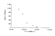
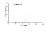
- FIG. 2B shows another combination pattern of impurity elements used for setting the main dopant and the sub-dopant. It is an example. It is a graph which shows the relationship between the doping concentration of a main dopant, and a minority carrier lifetime. It is a graph which shows the relationship between the thickness of a buffer layer, and the occurrence frequency of a strip-like stacking fault. It is a graph which shows the relationship between the minority carrier lifetime and the occurrence frequency of strip-like stacking faults.
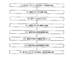
- a substrate made of SiC is prepared and transferred into an epitaxial growth furnace (step S1).
- hydrogen (H 2 ) gas is introduced into the furnace, the pressure is adjusted to about 1300 to 40000 Pa, and then the temperature is raised to 1600 to 1700 ° C. (step S2).
- introduction of a SiC source gas step S3
- introduction of a main dopant gas containing a main dopant that determines the conductivity type step S4
- introduction of a subdopant gas containing a subdopant that captures minority carriers step S5
- Steps S3 to S5 may be performed simultaneously, or the timing may be shifted, for example, step S5 may be performed slightly later than S4. Up to this point, a buffer layer mainly composed of SiC that promotes the capture and annihilation of minority carriers flowing from the breakdown voltage maintaining layer toward the substrate is formed on the substrate.
- step S6 the supply of the sub-dopant gas is stopped, and the flow rates of the SiC source gas and the main dopant gas are adjusted so as to form the pressure resistant maintenance layer (step S6).
- a breakdown voltage maintaining layer having a higher resistance than the buffer layer is formed on the buffer layer. That is, the buffer layer and the withstand voltage maintaining layer are configured such that the buffer layer has a lower resistance than the withstand voltage maintaining layer.
- the wafer (substrate) is carried out of the furnace (step S8).
- the buffer layer and the breakdown voltage maintaining layer are formed continuously, but may be formed separately.
- steps S1 to S5 steps S7 to S8 are performed to form a buffer layer, and then a process equivalent to steps S1 to S4 and S7 to S8 is performed to form a breakdown voltage maintaining layer.
- steps S1 to S4 and S7 to S8 are performed to form a breakdown voltage maintaining layer.
- the impurity element nitrogen (N) forming the donor level is selected as the main dopant.
- an impurity element to be a sub-dopant at least one or more of aluminum (Al), boron (B), vanadium (V), titanium (Ti), iron (Fe), and chromium (Cr) can be selected. It is.
- Al as an impurity element that forms an acceptor level is selected as a main dopant
- N, B, V, Ti, Fe, and Cr are used as impurity elements as sub-dopants. Etc., at least one of them can be selected.
- the doping concentration of the sub-dopant is preferably lower than that of the main dopant and about 1 ⁇ 10 14 cm ⁇ 3 or more and less than about 5 ⁇ 10 18 cm ⁇ 3 .
- the doping concentration of the sub-dopant is less than about 1 ⁇ 10 14 cm ⁇ 3 , minority carriers are not captured sufficiently, and the occurrence of strip stacking faults cannot be effectively prevented.
- the doping concentration of the sub-dopant is not more than about 5 ⁇ 10 18 cm ⁇ 3 even if it is lower than the doping concentration of the main dopant, the doping concentration becomes too high, increasing the resistance in the epi layer and decreasing the dielectric breakdown electric field. The problem such as becomes larger.
- the lifetime of minority carriers decreases as the doping concentration of the main dopant increases.
- the lifetime of minority carriers in a region where the doping concentration is on the order of 1 ⁇ 10 17 cm ⁇ 3 is about 700 ns or 1000 ns, whereas in a high concentration region where the doping concentration is about 1 ⁇ 10 18 cm ⁇ 3 or more.
- the lifetime of minority carriers is as short as about 300 ns or less. This is presumably due to the Auger recombination mechanism.
- the doping concentration of the main dopant is about 1 ⁇ 10 19 cm ⁇ 3 or more, a Double Shockley type stacking fault is likely to occur. Therefore, the doping concentration of the main dopant is desirably about 1 ⁇ 10 18 cm ⁇ 3 or more and less than about 1 ⁇ 10 19 cm ⁇ 3 .
- the doping concentration of the main dopant is increased and the thickness of the n-type buffer layer is changed so that the minority carrier lifetime at about 250 ° C. is about 120 ns.
- An n ⁇ type breakdown voltage maintaining layer for maintaining the breakdown voltage of the semiconductor device is stacked on the buffer layer of the pin diode, and is formed as a high resistance epi layer.
- the thickness of the breakdown voltage maintaining layer is about 10 ⁇ m, and the doping concentration of the impurity element is about 1 ⁇ 10 16 cm ⁇ 3 .
- a p-type anode region is formed on a part of the upper portion of the breakdown voltage maintaining layer by ion implantation of Al as an impurity element.
- the anode region thickness is set to about 0.3 ⁇ m, and the Al doping concentration is set to a box profile of about 1 ⁇ 10 20 cm ⁇ 3 .
- An anode electrode is formed on the upper surface of the anode region, and a cathode electrode is formed on the lower surface of the substrate forming the n-type cathode region on the back side.
- Al is ion-implanted around the anode region above the breakdown voltage maintaining layer to further form a p-type semiconductor region having a lower concentration than the anode region, thereby terminating the junction. (JTE) structure.
- the thickness of the buffer layer is at least 10 ⁇ m or more in order to reduce the occurrence of strip stacking faults to zero, and 15 ⁇ m or more to increase the reliability. It is desirable that
- the present inventors have attempted to further shorten the minority carrier lifetime, and have attempted to reduce the thickness of the buffer layer forming the changing point at which the occurrence frequency of the band-like stacking fault becomes zero. Further, for example, even when the buffer layer is formed with the thickness being suppressed to about 5 ⁇ m or less, it has been found that the occurrence frequency of the band-like stacking fault can be remarkably reduced. An example of the results of experiments conducted based on this finding is shown in the graph of FIG.
- a buffer layer is formed on an epitaxial wafer with a thickness of about 5 ⁇ m and a minority carrier lifetime being changed, and a pin diode using this epitaxial wafer as a semiconductor wafer is provided with 1 at 600 A / cm 2 .
- the figure shows the result of conducting the energization for about an hour and investigating the correlation between the minority carrier lifetime and the occurrence frequency of the band-like stacking fault.
- the shorter the minority carrier lifetime the lower the frequency of occurrence of strip stacking faults.
- the occurrence frequency of the strip-like stacking fault becomes zero.
- the minority carrier lifetime is 100 ns or less, the occurrence frequency of the strip-like stacking fault becomes zero.
- the minority carrier lifetime is sufficiently increased. It is difficult to make it smaller. Therefore, the authors were able to obtain a short minority carrier lifetime of 100 ns or less by increasing the concentration of the subdopant that forms a deep level.
- the buffer layer thickness is preferably about 0.1 ⁇ m or more and 5 ⁇ m or less.
- Japanese Patent No. 4364945 discloses introducing impurities that form recombination centers during epitaxial growth in order to shorten the minority carrier lifetime.
- the reduction of the minority carrier lifetime due to the conventional recombination center is less effective at a high temperature of about 150 ° C. or more, resulting in a long lifetime.
- the minority carrier lifetime is At 150 ° C., it exceeds 40 ns, and when the temperature is 250 ° C., it reaches 170 ns or more.
- the method proposed by the inventors to increase the concentration of the main dopant to about 1 ⁇ 10 18 cm ⁇ 3 or more is short even at a high temperature of about 150 ° C. or more, as indicated by the diamond data points in FIG. It has been found that the minority carrier life can be maintained.
- the concentration of N as the main dopant was set to about 5 ⁇ 10 18 cm ⁇ 3 .
- the minority carrier lifetime remained at about 20 ns even when the temperature was 150 ° C., and even when the temperature further increased to 250 ° C., it could be suppressed to less than 60 ns. This is thought to be because the recombination mechanism due to the recombination centers does not work effectively at high temperatures, whereas the method proposed by the inventors uses the Auger recombination mechanism and is less temperature dependent.
- an epitaxial wafer as shown in the sectional view of FIG. 7 is prepared as a semiconductor wafer.
- a substrate 21 made of n + type SiC serving as a cathode region a high concentration n + type buffer layer 22 provided on the substrate 21, and a buffer layer 22 provided on the buffer layer 22.
- An epitaxial wafer having a three-layer structure of a low concentration n ⁇ -type withstand voltage maintaining layer 23 is illustrated.
- the breakdown voltage maintaining layer 23 functions as an intrinsic semiconductor layer (i layer) of the pin diode.
- p-type Al ions are implanted into the surface of the breakdown voltage maintaining layer 23 opposite to the buffer layer 22 by, for example, ion implantation, and a predetermined activation process is performed after the implantation.
- a high-concentration p + -type anode region 24 is formed in part of the upper portion of the breakdown voltage maintaining layer 23.
- the anode region 24 corresponds to the “second conductivity type semiconductor region” of the present invention.
- Al ions are further implanted to form p-type semiconductor regions 25, having a lower concentration than the anode region 24.
- a pin diode when 25 is formed is illustrated.
- an anode electrode 27 is formed on the upper surface of the anode region 24 with nickel (Ni) or the like, and the substrate 21 on the back surface side is used as the cathode region and is formed on the lower surface of the cathode region.
- a cathode electrode 26 is formed.
- the buffer layer 22 of the epitaxial wafer is actively promoted to capture minority carriers, thereby suppressing the thickness of the buffer layer 22 and increasing the current.
- a semiconductor device that can effectively suppress the occurrence of strip-like stacking faults extending from the interface between the buffer layer 22 and the substrate 21 when the bipolar operation is performed can be manufactured.
- Example 1 using the method for manufacturing a semiconductor device according to the first embodiment will be described.
- the substrate 21 made of a SiC substrate having a diameter ( ⁇ ) of 3 inches obtained by chemical mechanical polishing (CMP) of the Si surface of the substrate 21 made of n + -type 4H—SiC, which is turned off by 4 ° in the ⁇ 11-20> direction.
- CMP chemical mechanical polishing
- the substrate 21 made of a SiC substrate having a diameter ( ⁇ ) of 3 inches obtained by chemical mechanical polishing (CMP) of the Si surface of the substrate 21 made of n + -type 4H—SiC, which is turned off by 4 ° in the ⁇ 11-20> direction.
- CMP chemical mechanical polishing
- H 2 as a raw material gas has a flow rate of about 1.69 ⁇ 10 2 Pa ⁇ m 3 / s (about 100 slm), and monosilane (SiH 4 ) has a flow rate of about 143.
- an epitaxial growth layer having a thickness of about 5 ⁇ m is formed on the Si surface side of the substrate 21, and N is added at a doping concentration of about 5 ⁇ 10 18 cm ⁇ 3 and B is added at a doping concentration of about 1 ⁇ 10 15 cm ⁇ 3.
- Layer 22 was formed. That is, in Example 1, the buffer layer 22 was epitaxially grown inside the epitaxial growth apparatus by simultaneously adding N and B to the SiC single crystal layer simultaneously while controlling the respective doping concentrations.
- SiH 4 is supplied at a flow rate of about 312.65 ⁇ 10 ⁇ 3 Pa ⁇ m 3 / s (about 185 sccm)
- C 3 H 8 is supplied at a flow rate of about 116.61 ⁇ 10 ⁇ 3 Pa. ⁇ M 3 / s (about 69 sccm) and N 2 were respectively changed to a flow rate of about 8.45 ⁇ 10 ⁇ 3 Pa ⁇ m 3 / s (about 5 sccm), and the other source gas introduction conditions were the same.
- the SiC single crystal layer was epitaxially grown for about 7 hours.
- a breakdown voltage maintaining layer 23 doped with N at a doping concentration of about 1 ⁇ 10 14 cm ⁇ 3 was epitaxially grown to a thickness of about 120 ⁇ m.
- an anode region 24 having a box profile with a thickness of about 0.3 ⁇ m and a doping concentration of about 1 ⁇ 10 20 cm ⁇ 3 is implanted into a part of the upper portion of the breakdown voltage maintaining layer 23 by ion implantation of Al as an impurity element. Formed.
- Al ions are implanted around the anode region 24 above the breakdown voltage maintaining layer 23 to form p-type semiconductor regions 25 and 25 having a lower concentration than the anode region 24. Further, a plurality of pin diodes having a JTE structure were formed.
- the minority carrier lifetime at 250 ° C. of the buffer layer 22 was set to 50 ns by adjusting the doping concentrations of the main dopant and the sub-dopant. Then, each pin diode was subjected to an energization experiment at 600 A / cm 2 for about 1 hour, and the occurrence frequency of strip-like stacking faults was examined. As a result of the energization experiment, even when the buffer layer 22 has a thickness of about 5 ⁇ m, no strip-like stacking fault occurs in the pin diode according to Example 1, and the thickness of the buffer layer 22 is suppressed and the pin as a product is produced. It has been found that the improvement in the quality of the diode can be suitably achieved.
- a pin diode in which the minority carrier lifetime was not controlled by adjusting the doping concentrations of the main dopant and the sub-dopant was prepared as a comparative example.
- the pin diode according to the comparative example was subjected to a bipolar operation by conducting the same energization experiment as in Example 1. Then, the anode electrode was peeled off, and a band-pass filter near 420 nm at room temperature was used for the epitaxial wafer. The photoluminescence emission was measured.
- the pin diode according to the comparative example as shown by the substantially trapezoidal region that is whitened in the top view of FIG.
- FIG. 10 shows a state in which the strip-like stacking fault SFb extending long across the upper and lower ends of the epitaxial wafer emits light together with the triangular stacking faults SFt 1 and SFt 2 .
- steps S1 to S4 and S7 to S8 in FIG. 1 are performed (step Sa), and a wafer (underlying substrate) in which the buffer layer 22 doped with only the main dopant is formed on the substrate 21 is manufactured. Thereafter, ion implantation of a sub-dopant is performed on the wafer using an ion implantation apparatus (steps S9 to S11). Subsequently, the wafer is heat-treated using an activation heat treatment apparatus to activate the implanted ions (steps S12 to S14). Thereafter, steps S1 to S4 and S7 to S8 in FIG. Form (step Sb).
- the activation heat treatment is performed subsequently after the ion implantation. However, the activation heat treatment may be performed after the breakdown voltage maintaining layer 23 is formed. In that case, S12 to S14 are performed after step Sb.
- the epitaxial wafer according to the second embodiment is manufactured.
- the semiconductor device manufacturing method according to the second embodiment is the same as the semiconductor device manufacturing method according to the first embodiment described with reference to FIGS. To do.
- a bipolar operation is performed with a large current while suppressing the thickness of the buffer layer 22. In this case, it is possible to manufacture a semiconductor device that can effectively suppress the occurrence of strip-like stacking faults extending from the interface between the buffer layer 22 and the substrate 21.
- Example 2 using the semiconductor device manufacturing method according to the second embodiment will be described.
- a substrate 21 made of a SiC substrate having a diameter ( ⁇ ) of 3 inches obtained by chemically and mechanically polishing (CMP) the Si surface of the substrate 21 made of n + -type 4H—SiC off by 4 ° in the ⁇ 11-20> direction, Placed in an epitaxial growth apparatus.
- CMP chemically and mechanically polishing
- H 2 as a source gas has a flow rate of about 1.69 ⁇ 10 2 Pa ⁇ m 3 / s (about 100 slm)
- SiH 4 has a flow rate of about 143.65 ⁇ .
- the substrate 21 on which the single crystal layer of SiC is formed is transferred to the ion implantation apparatus 50 and fixed inside the implantation chamber 57, and V ions are about 7 ⁇ 10 11 cm ⁇ 2 in the single crystal layer.
- the dose was injected at a dose of. V is a minor dopant.
- the substrate 21 was heat-treated for activation, and V was lower than the doping concentration of the main dopant, and was added within a range of about 1 ⁇ 10 14 cm ⁇ 3 or more and less than about 5 ⁇ 10 18 cm ⁇ 3 .
- a buffer layer 22 was formed.
- SiH 4 is supplied at a flow rate of about 312.65 ⁇ 10 ⁇ 3 Pa ⁇ m 3 / s (about 185 sccm)
- C 3 H 8 is supplied at a flow rate of about 116.61 ⁇ 10 ⁇ 3 Pa ⁇ m 3 / s (about 69 sccm) and N 2 are respectively changed to a flow rate of about 8.45 ⁇ 10 ⁇ 3 Pa ⁇ m 3 / s (about 5 sccm), and other source gases
- a breakdown voltage maintaining layer 23 to which N was added at a doping concentration of about 1 ⁇ 10 14 cm ⁇ 3 was epitaxially grown to a thickness of about 120 ⁇ m.
- a part of the upper portion of the breakdown voltage maintaining layer 23 is ion-implanted with Al as an impurity element, and the p + type is set to a box profile with a thickness of about 0.3 ⁇ m and a doping concentration of about 1 ⁇ 10 20 cm ⁇ 3.
- the anode region 24 was formed.
- An anode electrode 27 was formed on the upper surface of the anode region 24, and a cathode electrode 26 was formed on the lower surface of the substrate 21.
- Al is ion-implanted around the anode region 24 above the breakdown voltage maintaining layer 23 to further form a p-type semiconductor region 25 having a lower concentration than the anode region 24.
- a plurality of pin diodes having a JTE structure were manufactured.
- the minority carrier lifetime at 250 ° C. of the buffer layer 22 was set by controlling it to 80 ns by adjusting the doping concentrations of the main dopant and the sub-dopant. Then, each pin diode was subjected to an energization experiment at 600 A / cm 2 for about 1 hour, and the occurrence frequency of strip-like stacking faults was examined. As a result of the energization experiment, the pin diode according to Example 2 in which the buffer layer 22 was formed by ion implantation did not cause any strip-like stacking fault even when the buffer layer 22 had a thickness of about 5 ⁇ m. As in the case of, it has been found that the suppression of the thickness of the buffer layer 22 and the improvement of the quality of the pin diode as a product can be suitably achieved.
- the pin diode has been described as an example.
- the semiconductor device is not limited to the pin diode.
- an “pn diode” in which an i layer or a semiconductor layer having a low concentration that can be approximated to an i layer is not sandwiched between pn junctions, or a “p + n + diode” such as a Zener diode or a tunnel diode may be used. Absent.
- heterojunction bipolar transistor HBT
- a heterojunction bipolar transistor using a heterojunction of SiC and a semiconductor material having a different forbidden band width between an emitter and a base.
- a forward current flows through the body diode of the MOSFET at the time of switching. Therefore, the application of the present invention is effective in suppressing the occurrence of strip-like stacking faults.
- the present invention is also effective in preventing the occurrence of strip-like stacking faults having other forms.
- a rectangular belt-like stacking fault, or a strip-like stacking fault that has a rectangular shape with a long side of a rectangular sawtooth, or a strip-like stacking fault that has a trapezoidal height or a width corresponding to the short side of the rectangle is not constant.
- the present invention includes various embodiments and the like not described above, and the technical scope of the present invention is defined only by the invention specifying matters according to the appropriate claims from the above description. Is.
Landscapes
- Chemical & Material Sciences (AREA)
- Metallurgy (AREA)
- Engineering & Computer Science (AREA)
- Materials Engineering (AREA)
- Organic Chemistry (AREA)
- Chemical Kinetics & Catalysis (AREA)
- General Chemical & Material Sciences (AREA)
- Crystallography & Structural Chemistry (AREA)
- Inorganic Chemistry (AREA)
- Mechanical Engineering (AREA)
- Recrystallisation Techniques (AREA)
- Chemical Vapour Deposition (AREA)
- Crystals, And After-Treatments Of Crystals (AREA)
Abstract
エピタキシャル成長層の厚みを抑制しつつ、大電流でバイポーラ動作させても、基板上のエピタキシャル成長層と基板との界面から拡張する帯状積層欠陥の発生を効果的に抑制するエピタキシャルウェハを提供する。エピタキシャルウェハの製造方法は、炭化珪素の基板の上に、導電型を決める主ドーパントを添加すると共に少数キャリアを捕獲する副ドーパントを主ドーパントのドーピング濃度より低いドーピング濃度で添加して、耐圧維持層から基板の方向に流れる少数キャリアの捕獲及び消滅を促進する、耐圧維持層より低抵抗の、炭化珪素を主成分とするバッファ層をエピタキシャル成長するステップ(S1~S5)と、バッファ層の上に耐圧維持層をエピタキシャル成長するステップと、を含む。
Description
本発明は、エピタキシャルウェハの製造方法、エピタキシャルウェハ、半導体装置の製造方法及び半導体装置に関し、特に炭化珪素半導体を用いたエピタキシャルウェハを製造する技術に関する。
基板上に炭化珪素(SiC)をエピタキシャル成長させたエピタキシャルウェハには、多くの結晶欠陥・転位が存在しており、これらがSiC半導体装置の特性に悪影響を与えていると考えられている。特にエピタキシャル成長層中の基底面転位(BPD)は、半導体装置をバイポーラ動作させた際に積層欠陥に拡張し、電流を流れにくくすることにより半導体装置のオン電圧を上昇させ「バイポーラ劣化」の発生につながる。
BPDは基板に数百~数千個/cm2の密度で存在する。その多くはエピタキシャル成長中に貫通刃状転位(TED)に変換されるが、残ったBPDは表面まで貫通し、三角形状の積層欠陥に拡張して問題となる。この問題は、エピタキシャル成長条件の工夫等により変換の効率が上昇し、ほぼ全てのBPDが変換されるようになることで改善が進んでいる。しかしながら、近年、積層欠陥が帯状に広がることが報告されており、バイポーラ動作をするSiC半導体装置の実用化に向けた新たな問題となっている(非特許文献1参照。)。
非特許文献1には、帯状積層欠陥が広がる原因として、半導体基板中での電子―ホールの再結合が挙げられており、この再結合を抑制するため、半導体装置の半導体基板の上にエピタキシャル成長したバッファ層を厚くすることにより、半導体基板への過剰なホール注入を防ぐ対策が開示されている。しかしながら厚いバッファ層の成膜は、エピ成長のスループット低下によるコスト増大、欠陥密度増化による歩留まり低下及びエピタキシャルウェハの抵抗増大につながるため望ましくない。よって最小限のバッファ層の厚みで、帯状積層欠陥を防ぐ対策が必要とされていた。
J.J.スマーケリス(Sumakeris)他、「バイポーラ型SiC半導体装置の順方向電圧安定化へのアプローチ(Approaches to Stabilizing the Forward Voltage of Bipolar SiC Devices)」、(米国)、マテリアルサイエンスフォーラム(Materials Science Forum)、オンライン 第457-460巻、2004年、p.1113-1116
本発明は上記した問題に着目して為されたものであって、エピタキシャル成長層の厚みを抑制しつつ、大電流でバイポーラ動作させても、基板上のエピタキシャル成長層と基板との界面から拡張する帯状積層欠陥の発生を効果的に抑制するエピタキシャルウェハの製造方法、エピタキシャルウェハ、半導体装置の製造方法及び半導体装置を提供することを目的とする。
上記課題を解決するために、本発明に係るエピタキシャルウェハの製造方法のある態様は、炭化珪素の基板と耐圧維持層とを備えるエピタキシャルウェハの製造方法において、基板の上に、導電型を決める主ドーパントを添加すると共に少数キャリアを捕獲する副ドーパントを主ドーパントのドーピング濃度より低いドーピング濃度で添加して、耐圧維持層から基板の方向に流れる少数キャリアの捕獲及び消滅を促進する、耐圧維持層より低抵抗の、炭化珪素を主成分とするバッファ層をエピタキシャル成長するステップと、バッファ層の上に耐圧維持層をエピタキシャル成長するステップと、を含むことを要旨とする。
また本発明に係るエピタキシャルウェハの製造方法の他の態様は、炭化珪素の基板と耐圧維持層とを備えるエピタキシャルウェハの製造方法において、基板の上に、導電型を決める主ドーパントを添加しながら炭化珪素を主成分とする単結晶層をエピタキシャル成長するステップと、単結晶層に、少数キャリアを捕獲する副ドーパントのイオンを主ドーパントのドーピング濃度より低いドーピング濃度となるドーズ量でイオン注入するステップと、イオンを活性化して、耐圧維持層から基板の方向に流れる少数キャリアの捕獲及び消滅を促進する、耐圧維持層より低抵抗の、バッファ層を単結晶層によって形成するステップと、バッファ層の上に耐圧維持層をエピタキシャル成長するステップと、を含むことを要旨とする。
また本発明に係る本発明に係るエピタキシャルウェハのある態様は、炭化珪素の基板と耐圧維持層とを備えるエピタキシャルウェハにおいて、基板と耐圧維持層の間に設けられた、導電型を決める主ドーパントと、少数キャリアを捕獲し主ドーパントのドーピング濃度より低いドーピング濃度の副ドーパントとが添加された、耐圧維持層から基板の方向に流れる少数キャリアの捕獲及び消滅を促進する、耐圧維持層より低抵抗の、炭化珪素を主成分とするバッファ層を備えることを要旨とする。
また本発明に係る半導体装置の製造方法のある態様は、上記したある態様に係るエピタキシャルウェハの製造方法を用いて製造した炭化珪素の基板と耐圧維持層とを備えるエピタキシャルウェハを用いた半導体装置の製造方法において、第1導電型の耐圧維持層の上部の一部に第2導電型の半導体領域を形成する工程を含むことを要旨とする。
また本発明に係る半導体装置の製造方法の他の態様は、上記した他の態様に係るエピタキシャルウェハの製造方法を用いて製造した炭化珪素の基板と耐圧維持層とを備えるエピタキシャルウェハを用いた半導体装置の製造方法において、第1導電型の耐圧維持層の上部の一部に第2導電型の半導体領域を形成する工程を含むことを要旨とする。
また本発明に係る半導体装置のある態様は、上記したある態様に係る炭化珪素の基板と耐圧維持層とを備えるエピタキシャルウェハを用いた半導体装置において、第1導電型の耐圧維持層の上部の一部に設けられた第2導電型の半導体領域を備えることを要旨とする。
従って本発明に係るエピタキシャルウェハの製造方法、エピタキシャルウェハ、半導体装置の製造方法及び半導体装置によれば、エピタキシャル成長層の厚みを抑制しつつ、大電流でバイポーラ動作させても、基板上のエピタキシャル成長層と基板との界面から拡張する帯状積層欠陥の発生を効果的に抑制することができる。
以下に本発明の第1及び第2の実施の形態を説明する。以下の図面の記載において、同一又は類似の部分には同一又は類似の符号を付している。但し、図面は模式的なものであり、厚みと平面寸法との関係、各装置や各部材の厚みの比率等は現実のものとは異なることに留意すべきである。したがって、具体的な厚みや寸法は以下の説明を参酌して判定すべきものである。また、図面相互間においても互いの寸法の関係や比率が異なる部分が含まれていることは勿論である。
また、以下の説明における「左右」や「上下」の方向は、単に説明の便宜上の定義であって、本発明の技術的思想を限定するものではない。よって、例えば、紙面を90度回転すれば「左右」と「上下」とは交換して読まれ、紙面を180度回転すれば「左」が「右」に、「右」が「左」になることは勿論である。また本明細書及び添付図面においては、n又はpを冠した領域や層では、それぞれ電子又は正孔が多数キャリアであることを意味する。またnやpに付す+や-は、+及び-が付記されていない半導体領域に比して、それぞれ相対的に不純物濃度が高い又は低い半導体領域であることを意味する。
<第1の実施の形態>
(エピタキシャルウェハの製造方法)
第1の実施の形態に係るエピタキシャルウェハの製造方法を、図1のフローチャートを参照して説明する。
まずSiCからなる基板を用意し、エピタキシャル成長炉内に搬送する(ステップS1)。次に炉内に水素(H2)ガスを導入し、1300~40000Pa程度の圧力を調整した後、1600~1700℃に昇温する(ステップS2)。その後、SiC原料ガスの導入(ステップS3)、導電型を決める主ドーパントを含む主ドーパントガスの導入(ステップS4)、少数キャリアを捕獲する副ドーパントを含む副ドーパントガスの導入(ステップS5)を行う。ステップS3~S5は同時でも、或いは例えばステップS5をS4より僅かに遅らせて行う等タイミングをずらしても構わない。ここまでで基板の上に、耐圧維持層から基板の方向に流れる少数キャリアの捕獲及び消滅を促進する、SiCを主成分とするバッファ層が形成される。
(エピタキシャルウェハの製造方法)
第1の実施の形態に係るエピタキシャルウェハの製造方法を、図1のフローチャートを参照して説明する。
まずSiCからなる基板を用意し、エピタキシャル成長炉内に搬送する(ステップS1)。次に炉内に水素(H2)ガスを導入し、1300~40000Pa程度の圧力を調整した後、1600~1700℃に昇温する(ステップS2)。その後、SiC原料ガスの導入(ステップS3)、導電型を決める主ドーパントを含む主ドーパントガスの導入(ステップS4)、少数キャリアを捕獲する副ドーパントを含む副ドーパントガスの導入(ステップS5)を行う。ステップS3~S5は同時でも、或いは例えばステップS5をS4より僅かに遅らせて行う等タイミングをずらしても構わない。ここまでで基板の上に、耐圧維持層から基板の方向に流れる少数キャリアの捕獲及び消滅を促進する、SiCを主成分とするバッファ層が形成される。
続いて副ドーパントガスの供給を停止し、SiC原料ガス、主ドーパントガスの流量を、耐圧維持層を形成するように調整する(ステップS6)。これによりバッファ層より高抵抗の耐圧維持層がバッファ層の上に形成される。すなわちバッファ層が耐圧維持層より低抵抗であるように、バッファ層及び耐圧維持層は構成されている。その後、降温、不活性ガス置換(ステップS7)を行った後に、ウェハ(基板)を炉外に搬出する(ステップS8)。上記はバッファ層と耐圧維持層を連続して形成する場合であるが、別々に形成する場合もあり得る。その際は、ステップS1~S5の後にステップS7~S8を行いバッファ層を形成した後に、ステップS1~S4、S7~S8とそれぞれ等価な処理を行い耐圧維持層を形成する処理を行う。以上のようにして第1の実施の形態に関わるエピタキシャルウェハが製造される。
第1の実施の形態における主ドーパントと副ドーパントの組み合わせパターンとしては、例えば図2(a)に示すように、主ドーパントとしてドナーレベルを形成する不純物元素の窒素(N)を選択した場合には、副ドーパントとなる不純物元素としては、アルミニウム(Al)、ボロン(B)、バナジウム(V)、チタン(Ti)、鉄(Fe)及びクロム(Cr)等のうち、少なくとも1種類以上が選択可能である。
また図2(b)に示すように、主ドーパントとしてアクセプタレベルを形成する不純物元素のAlを選択した場合には、副ドーパントとなる不純物元素としては、N、B、V、Ti、Fe及びCr等のうち少なくとも1種類以上が選択可能である。
また図2(b)に示すように、主ドーパントとしてアクセプタレベルを形成する不純物元素のAlを選択した場合には、副ドーパントとなる不純物元素としては、N、B、V、Ti、Fe及びCr等のうち少なくとも1種類以上が選択可能である。
副ドーパントのドーピング濃度は、主ドーパントより低濃度、かつ、1×1014cm-3程度以上、5×1018cm-3程度未満であることが望ましい。副ドーパントのドーピング濃度が1×1014cm-3程度未満の場合、少数キャリアの捕獲が不十分であり、帯状積層欠陥の発生を有効に防止することができない。一方、副ドーパントのドーピング濃度が、主ドーパントのドーピング濃度以下であっても5×1018cm-3程度以上の場合、ドーピング濃度が高くなりすぎ、エピ層における抵抗の増加や絶縁破壊電界の低下等の問題が大きくなる。
また図3のグラフ図に示すように、主ドーパントのドーピング濃度が高くなるほど、少数キャリアの寿命は短くなる。特に、ドーピング濃度が1×1017cm-3オーダレベルの領域における少数キャリアの寿命が700ns程度や1000ns程度であるのに対し、ドーピング濃度が1×1018cm-3程度以上の高濃度領域では、少数キャリアの寿命は約300ns程度以下と、非常に短くなることがわかる。これはオージェ再結合メカニズムによるものと推測される。
一方、主ドーパントのドーピング濃度が、1×1019cm-3程度以上であると、ダブルショックレー(Double Shockley)型の積層欠陥が発生し易くなる。そのため主ドーパントのドーピング濃度は、1×1018cm-3程度以上、1×1019cm-3程度未満であることが望ましい。
一方、主ドーパントのドーピング濃度が、1×1019cm-3程度以上であると、ダブルショックレー(Double Shockley)型の積層欠陥が発生し易くなる。そのため主ドーパントのドーピング濃度は、1×1018cm-3程度以上、1×1019cm-3程度未満であることが望ましい。
図4で採用したpinダイオードのバッファ層では、約250℃における少数キャリア寿命が120ns程度であるように、主ドーパントのドーピング濃度を高めて、n型のバッファ層の厚みを変化させている。
またpinダイオードのバッファ層の上には、半導体装置の耐圧を維持するためのn―型の耐圧維持層を積層し、高抵抗のエピ層として成膜している。耐圧維持層の厚みは約10μm、不純物元素のドーピング濃度は約1×1016cm-3程度である。
またpinダイオードのバッファ層の上には、半導体装置の耐圧を維持するためのn―型の耐圧維持層を積層し、高抵抗のエピ層として成膜している。耐圧維持層の厚みは約10μm、不純物元素のドーピング濃度は約1×1016cm-3程度である。
また耐圧維持層の上部の一部には、Alを不純物元素としてイオン注入して、p型のアノード領域を形成している。アノード領域の厚みは約0.3μm、Alのドーピング濃度は約1×1020cm-3程度のボックスプロファイルに設定している。またアノード領域の上面にはアノード電極を成膜して設けると共に、裏面側でn型のカソード領域をなす基板の下面には、カソード電極を成膜して設けている。またpinダイオードの端部の耐圧を向上させるために、耐圧維持層の上部のアノード領域の周囲にAlをイオン注入して、アノード領域より低濃度のp型の半導体領域をさらに形成し、接合終端(JTE)構造を具備させている。
図4に示すように、エピタキシャルウェハのバッファ層の厚みが厚くなるほど、帯状積層欠陥の発生頻度は低下していることがわかる。図4の結果より、少数キャリア寿命が120ns程度である場合、帯状積層欠陥の発生を零(ゼロ)にするには、バッファ層の厚みは少なくとも10μm以上、より確実性を高めるためには15μm以上であることが望ましい。
しかしバッファ層の厚みを厚くすると、エピタキシャル成長時の成膜プロセスのコストが増大する。そこで本発明者らは、研究の結果、少数キャリア寿命を更に短くすることを試み、帯状積層欠陥の発生頻度が零となる変化点をなすバッファ層の厚みを小さくするように試みた。そして、例えば厚みを5μm程度以下に抑えてバッファ層を成膜した場合であっても、帯状積層欠陥の発生頻度を著しく低下させることができるという知見を得た。この知見に基づいて行われた実験結果の一例を図5のグラフ図に示す。
図5中には、エピタキシャルウェハに、厚みを約5μmとし、少数キャリア寿命を変化させて成膜したバッファ層を設け、このエピタキシャルウェハを半導体ウェハとして用いたpinダイオードに、600A/cm2で1時間程度の通電を行い、少数キャリア寿命と帯状積層欠陥の発生頻度との相関を調べた結果が示されている。
図5に示したように、少数キャリア寿命を短くするほど、帯状積層欠陥の発生頻度が低下する。特に、少数キャリア寿命が100ns以下である場合、帯状積層欠陥の発生頻度が零となることがわかる。少数キャリア寿命を短くする方法としては、主ドーパントの濃度を高める方法が挙げられるが、先に述べたダブルショックレー(Double Shockley)型積層欠陥の発生の懸念があるために少数キャリア寿命を十分に小さくすることが困難である。そこで筆者らは深い準位を形成する副ドーパントの濃度を高めることにより、100ns以下の短い少数キャリア寿命を得ることができた。このようにして筆者らは5μm程度の実用的な膜厚のバッファ層で帯状積層欠陥の発生を防止することができた。原理的には少数キャリア寿命が短くなるほど、バッファ層膜厚を薄くすることができるが、0.1μm以下に薄くなると膜厚の制御が難しくなる。バッファ層膜厚としては0.1μm以上5μm以下程度が望ましい。
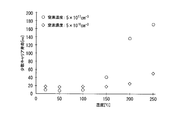
特許第4364945号公報では少数キャリア寿命を短くするために、エピタキシャル成長時に再結合中心を形成する不純物を導入することが示されている。しかしながら、発明者らが検討した結果、従来の再結合中心による少数キャリア寿命の低減は、150℃程度以上の高温にすると効果が薄れ、長寿命になってしまうことが判明した。例えば図6のグラフ図中の○印のデータ点で例示するように、主ドーパントであるNの濃度を5×1017cm-3程度としたときエピタキシャルウェハの場合、少数キャリア寿命は、温度が150℃では40nsを超え、更に温度が250℃では170ns以上に到達する。
一方で、発明者らが提案する主ドーパントの濃度を1×1018cm-3程度以上に高める方法では、図6中の菱形のデータ点で示すように、150℃程度以上の高温においても短い少数キャリア寿命を保てることが判明した。菱形のデータ点で示したエピタキシャルウェハは、主ドーパントであるNの濃度を5×1018cm-3程度とした。また少数キャリア寿命は、温度が150℃であっても20ns程度に留まると共に、更に温度が250℃に上昇しても、60ns未満に抑えることができた。これは再結合中心による再結合メカニズムは高温では有効に働かなくなる一方、発明者らの提案する手法はオージェ再結合メカニズムを利用しており温度依存性が小さいためと考えられる。
(半導体装置の製造方法)
次に、第1の実施の形態に係る半導体装置の製造方法を、pinダイオードを製造する場合を例として、図7~図9を参照して説明する。
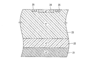
まず、図7の断面図で示したようなエピタキシャルウェハを半導体ウェハとして用意する。図7中には、カソード領域となるn+型のSiCからなる基板21、この基板21の上に設けられた高濃度のn+型のバッファ層22及びこのバッファ層22の上に設けられた低濃度のn-型の耐圧維持層23の3層構造を有するエピタキシャルウェハが例示されている。耐圧維持層23は、pinダイオードの真性半導体層(i層)として機能する。
次に、第1の実施の形態に係る半導体装置の製造方法を、pinダイオードを製造する場合を例として、図7~図9を参照して説明する。
まず、図7の断面図で示したようなエピタキシャルウェハを半導体ウェハとして用意する。図7中には、カソード領域となるn+型のSiCからなる基板21、この基板21の上に設けられた高濃度のn+型のバッファ層22及びこのバッファ層22の上に設けられた低濃度のn-型の耐圧維持層23の3層構造を有するエピタキシャルウェハが例示されている。耐圧維持層23は、pinダイオードの真性半導体層(i層)として機能する。
次に図8の断面図に示すように、p型を呈するAlイオンを耐圧維持層23のバッファ層22と反対側の表面に、例えばイオン注入法により注入すると共に、注入後に所定の活性化処理を施して、耐圧維持層23の上部の一部に高濃度のp+型のアノード領域24を形成する。アノード領域24は、本発明の「第2導電型の半導体領域」に相当する。尚、図8中には、アノード領域24の周囲の耐圧維持層23の上部にJTE構造をなすために、更にAlイオンを注入して、アノード領域24より低濃度のp型の半導体領域25,25が形成された場合のpinダイオードが例示されている。
次に図9の断面図に示すように、ニッケル(Ni)等で、アノード領域24の上面にアノード電極27を成膜すると共に、裏面側をなす基板21をカソード領域として、カソード領域の下面にカソード電極26を成膜する。図7~図9を参照して説明した一連の工程により、バッファ層22をカソード側に有するpinダイオードが、半導体装置として製造できる。
第1の実施の形態に係る半導体装置の製造方法によれば、エピタキシャルウェハのバッファ層22によって少数キャリアの捕獲を積極的に促進させることにより、バッファ層22の厚みを抑制しつつ、大電流でバイポーラ動作させた際にバッファ層22と基板21との界面から拡張する帯状積層欠陥の発生を効果的に抑制できる半導体装置を製造することができる。
次に、第1の実施の形態に係る半導体装置の製造方法を用いた実施例1を説明する。まず<11-20>方向に4°オフしたn+型の4H-SiCからなる基板21のSi面を、化学的機械研磨(CMP)した径(φ)3インチのSiC基板からなる基板21を、エピタキシャル成長装置の中に入れた。そして温度約1680℃で圧力10.3kPa程度の雰囲気中に、原料ガスとしてH2を流量約1.69×10²Pa・m3/s(約100slm)、モノシラン(SiH4)を流量約143.65×10-3Pa・m3/s(約85sccm)、プロパン(C3H8)を流量約38.87×10-3Pa・m3/s(約23sccm)、窒素(N2)を流量約84.5×10-3Pa・m3/s(約50sccm)及びトリエチルボロン(C6H15B)を流量約16.9×10-3Pa・m3/s(約10sccm)でそれぞれ導入して、30分間程度、SiCの単結晶層のエピタキシャル成長を行った。Nは主ドーパントであり、Bは副ドーパントである。
そして基板21のSi面側に、エピタキシャル成長層を厚さ約5μm成膜し、Nをドーピング濃度5×1018cm-3程度、Bをドーピング濃度1×1015cm-3程度でそれぞれ添加したバッファ層22を形成した。すなわち実施例1では、エピタキシャル成長装置の内側で、N及びBを並行して同時に、かつ、それぞれのドーピング濃度を制御してSiCの単結晶層に添加し、バッファ層22をエピタキシャル成長した。
次に、バッファ層22のエピタキシャル成長条件のうち、SiH4を流量約312.65×10⁻³Pa・m3/s(約185sccm)、C3H8を流量約116.61×10-3Pa・m3/s(約69sccm)及びN2を流量約8.45×10-3Pa・m3/s(約5sccm)にそれぞれ変更すると共に、他の原料ガスの導入条件は同じ条件で、7時間程度、SiCの単結晶層のエピタキシャル成長を行った。そしてバッファ層22の上に、Nをドーピング濃度1×1014cm-3程度で添加した耐圧維持層23を厚さ約120μmでエピタキシャル成長した。
そして耐圧維持層23の上部の一部に、Alを不純物元素としてイオン注入して、厚みを約0.3μm、ドーピング濃度を約1×1020cm-3程度のボックスプロファイルに設定したアノード領域24を形成した。またアノード領域24の上面にアノード電極27を成膜すると共に、基板21の下面にカソード電極26を成膜した。また半導体装置の端部の耐圧を向上させるために、耐圧維持層23の上部のアノード領域24の周囲にAlをイオン注入して、アノード領域24より低濃度のp型の半導体領域25,25をさらに形成し、JTE構造を備えるpinダイオードを複数個製造した。
尚、バッファ層22の250℃における少数キャリア寿命は、主ドーパント及び副ドーパントのドーピング濃度の調節により50nsに制御して設定した。そして、それぞれのpinダイオードに600A/cm2で1時間程度の通電実験を行い、帯状積層欠陥の発生頻度を調べた。
通電実験の結果、実施例1に係るpinダイオードには、バッファ層22が5μm程度の厚みであっても、帯状積層欠陥は一切発生せず、バッファ層22の厚みの抑制と、製品としてのpinダイオードの品質の向上とを好適に両立できることがわかった。
通電実験の結果、実施例1に係るpinダイオードには、バッファ層22が5μm程度の厚みであっても、帯状積層欠陥は一切発生せず、バッファ層22の厚みの抑制と、製品としてのpinダイオードの品質の向上とを好適に両立できることがわかった。
(比較例)
一方、主ドーパント、副ドーパントのドーピング濃度の調節による少数キャリア寿命の制御を行わなかったpinダイオードを比較例として用意した。そして比較例に係るpinダイオードを、実施例1の場合と同様の通電実験を行ってバイポーラ動作させた後、アノード電極を剥離し、室温で420nm近傍のバンドパスフィルターを用いて、エピタキシャルウェハに対してフォトルミネッセンス発光の測定を行った。その結果、比較例に係るpinダイオードには、図10の上面図中に白みがかった略台形状の領域で示すように、バッファ層22と基板21との界面から拡がる帯状積層欠陥SFbが観察された。図10中には、エピタキシャルウェハの上下の両端に亘って長く延びた帯状積層欠陥SFbが、三角形状積層欠陥SFt1,SFt2と共に発光した状態が示されている。
一方、主ドーパント、副ドーパントのドーピング濃度の調節による少数キャリア寿命の制御を行わなかったpinダイオードを比較例として用意した。そして比較例に係るpinダイオードを、実施例1の場合と同様の通電実験を行ってバイポーラ動作させた後、アノード電極を剥離し、室温で420nm近傍のバンドパスフィルターを用いて、エピタキシャルウェハに対してフォトルミネッセンス発光の測定を行った。その結果、比較例に係るpinダイオードには、図10の上面図中に白みがかった略台形状の領域で示すように、バッファ層22と基板21との界面から拡がる帯状積層欠陥SFbが観察された。図10中には、エピタキシャルウェハの上下の両端に亘って長く延びた帯状積層欠陥SFbが、三角形状積層欠陥SFt1,SFt2と共に発光した状態が示されている。
<第2の実施の形態>
第2の実施の形態における主ドーパントと副ドーパントの組み合わせパターン及びそれぞれの濃度は、第1の実施の形態の場合と同じである。
(エピタキシャルウェハの製造方法)
次に第2の実施形態に関わるエピタキシャルウェハの製造方法を図11をもとに説明する。
第2の実施の形態における主ドーパントと副ドーパントの組み合わせパターン及びそれぞれの濃度は、第1の実施の形態の場合と同じである。
(エピタキシャルウェハの製造方法)
次に第2の実施形態に関わるエピタキシャルウェハの製造方法を図11をもとに説明する。
まず図1のステップS1~S4、S7~S8を行い(ステップSa)、基板21上に主ドーパントのみをドープしたバッファ層22を形成したウェハ(下地基板)を作製する。その後、当該ウェハに対し、イオン注入装置を用いて副ドーパントのイオン注入を実施する(ステップS9~S11)。続いて活性化熱処理装置を用いて当該ウェハの熱処理を行い、注入したイオンを活性化する(ステップS12~S14)その後、図1のステップS1~S4、S7~S8を行い、耐圧維持層23を形成する(ステップSb)。上記はイオン注入の後に引き続いて活性化熱処理を実施する場合であるが、活性化熱処理を耐圧維持層23形成後に実施してもよい。その際は、S12~S14をステップSbの後に実施する。以上のようにして第2の実施形態に関わるエピタキシャルウェハを製造する。
(半導体装置の製造方法)
第2の実施の形態に係る半導体装置の製造方法については、図7~図9を参照して説明した第1の実施の形態に係る半導体装置の製造方法と同様であるため、重複説明を省略する。第2の実施の形態に係る半導体装置の製造方法によれば、第1の実施の形態に係る半導体装置の製造方法と同様に、バッファ層22の厚みを抑制しつつ、大電流でバイポーラ動作させた際にバッファ層22と基板21との界面から拡張する帯状積層欠陥の発生を効果的に抑制できる半導体装置を製造することができる。
第2の実施の形態に係る半導体装置の製造方法については、図7~図9を参照して説明した第1の実施の形態に係る半導体装置の製造方法と同様であるため、重複説明を省略する。第2の実施の形態に係る半導体装置の製造方法によれば、第1の実施の形態に係る半導体装置の製造方法と同様に、バッファ層22の厚みを抑制しつつ、大電流でバイポーラ動作させた際にバッファ層22と基板21との界面から拡張する帯状積層欠陥の発生を効果的に抑制できる半導体装置を製造することができる。
次に、第2の実施の形態に係る半導体装置の製造方法を用いた実施例2を説明する。<11-20>方向に4°オフしたn+型の4H-SiCからなる基板21のSi面を、化学的機械研磨(CMP)した径(φ)3インチのSiC基板からなる基板21を、エピタキシャル成長装置の中に入れた。そして温度約1680℃で圧力10.3kPa程度の雰囲気中に、原料ガスとしてH2を流量約1.69×10²Pa・m3/s(約100slm)、SiH4を流量約143.65×10-3Pa・m3/s(85sccm)、C3H8を流量約38.87×10-3Pa・m3/s(約23sccm)及びN2を流量約84.5×10-3Pa・m3/s(約50sccm)でそれぞれ導入して、30分間程度、SiCの単結晶層のエピタキシャル成長を行って、単結晶層を厚さ約5μm成膜した。Nは主ドーパントである。
次に、SiCの単結晶層が成膜された基板21をイオン注入装置50に搬送し、注入室57の内部に固定して、単結晶層にVイオンを、7×1011cm-2程度のドーズ量で注入した。Vは副ドーパントである。その後、基板21に活性化のための熱処理を施し、Vが主ドーパントのドーピング濃度より低く、1×1014cm-3程度以上、5×1018cm-3程度未満の範囲内で添加されたバッファ層22を形成した。
次に実施例1の場合と同様に、バッファ層22のエピタキシャル成長条件のうち、SiH4を流量約312.65×10⁻³Pa・m3/s(約185sccm)、C3H8を流量約116.61×10-3Pa・m3/s(約69sccm)及びN2を流量約8.45×10-3Pa・m3/s(約5sccm)にそれぞれ変更すると共に、他の原料ガスの導入条件は同じ条件で、7時間程度、SiCの単結晶層のエピタキシャル成長を行った。そしてバッファ層22の上に、Nをドーピング濃度1×1014cm-3程度で添加した耐圧維持層23を、厚さ約120μmでエピタキシャル成長した。
そして耐圧維持層23の上部の一部に、Alを不純物元素としてイオン注入して、厚みを約0.3μm、ドーピング濃度を約1×1020cm-3程度のボックスプロファイルに設定したp+型のアノード領域24を形成した。またアノード領域24の上面にアノード電極27を成膜すると共に、基板21の下面にカソード電極26を成膜した。また半導体装置の端部の耐圧を向上させるために、耐圧維持層23の上部のアノード領域24の周囲にAlをイオン注入して、アノード領域24より低濃度のp型の半導体領域25をさらに形成し、JTE構造を備えるpinダイオードを複数個製造した。
尚、バッファ層22の250℃における少数キャリア寿命は、主ドーパントおよび副ドーパントのドーピング濃度の調節により80nsに制御して設定した。そして、それぞれのpinダイオードに600A/cm2で1時間程度の通電実験を行い、帯状積層欠陥の発生頻度を調べた。
通電実験の結果、イオン注入を用いてバッファ層22を形成した実施例2に係るpinダイオードは、バッファ層22が5μm程度の厚みであっても、帯状積層欠陥は一切発生せず、実施例1の場合と同様に、バッファ層22の厚みの抑制と、製品としてのpinダイオードの品質の向上とを好適に両立できることがわかった。
通電実験の結果、イオン注入を用いてバッファ層22を形成した実施例2に係るpinダイオードは、バッファ層22が5μm程度の厚みであっても、帯状積層欠陥は一切発生せず、実施例1の場合と同様に、バッファ層22の厚みの抑制と、製品としてのpinダイオードの品質の向上とを好適に両立できることがわかった。
また第1及び第2の実施の形態に係る半導体装置の製造方法では、pinダイオードを例として説明したが、半導体装置としてはpinダイオードに限定されるものではない。例えば、i層若しくはi層に近似できる程度の低濃度の半導体層をpn接合の間に挟まない「pnダイオード」、又は、ツェナーダイオードやトンネルダイオードのような「p+n+ダイオード」等でも構わない。
更に本発明は、バイポーラトランジスタ、IGBT、サイリスタ等、各種のバイポーラ動作を行う半導体装置や、これらをモノシリックに集積化した半導体集積回路等に適用できる。図7~図9ではn+型の基板21の上にn+型のバッファ層22及びn-型の耐圧維持層23を備えた半導体装置を例示したが、これに限定されず、例えばp+型の基板の上にp+型のバッファ層及びn-型の耐圧維持層が設けられた構成であってもよい。
またSiCと、SiCとは禁制帯幅の異なる半導体材料とのヘテロ接合をエミッタ・ベース間等に用いたヘテロ接合バイポーラトランジスタ(HBT)等にも適用できる。更にMOSFETのようなユニポーラデバイスに適用した場合であっても、スイッチング時にMOSFETのボディダイオードに順方向電流が流れるため、本発明を適用すれば、帯状積層欠陥の発生の抑制に効果的である。
また図10中には帯状積層欠陥として、上面から見て上底及び下底が直線状の形態が例示されているが、本発明は他の形態を有する帯状積層欠陥の発生防止についても有効である。例えば矩形状の帯状積層欠陥、或いは矩形状であって矩形の長辺が鋸歯状であるような帯状積層欠陥、或いは台形の高さや矩形の短辺に相当する帯の幅が一定でない帯状積層欠陥等、各種の形態の帯状積層欠陥の発生を防止可能である。
以上のとおり本発明は、上記に記載していない様々な実施の形態等を含むとともに、本発明の技術的範囲は、上記の説明から妥当な特許請求の範囲に係る発明特定事項によってのみ定められるものである。
以上のとおり本発明は、上記に記載していない様々な実施の形態等を含むとともに、本発明の技術的範囲は、上記の説明から妥当な特許請求の範囲に係る発明特定事項によってのみ定められるものである。
21 基板(カソード領域)
22 バッファ層
23 耐圧維持層
24 アノード領域(半導体領域)
25 p型の半導体領域
26 カソード電極
27 アノード電極
SFb 帯状積層欠陥
SFt1,SFt2 三角形状積層欠陥
22 バッファ層
23 耐圧維持層
24 アノード領域(半導体領域)
25 p型の半導体領域
26 カソード電極
27 アノード電極
SFb 帯状積層欠陥
SFt1,SFt2 三角形状積層欠陥
Claims (13)
- 炭化珪素の基板と耐圧維持層とを備えるエピタキシャルウェハの製造方法において、
前記基板の上に、導電型を決める主ドーパントを添加すると共に少数キャリアを捕獲する副ドーパントを前記主ドーパントのドーピング濃度より低いドーピング濃度で添加して、前記耐圧維持層から前記基板の方向に流れる前記少数キャリアの捕獲及び消滅を促進する、前記耐圧維持層より低抵抗の、炭化珪素を主成分とするバッファ層をエピタキシャル成長するステップと、
前記バッファ層の上に前記耐圧維持層をエピタキシャル成長するステップと、
を含むことを特徴とするエピタキシャルウェハの製造方法。 - 前記主ドーパントを、1.0×1018cm-3以上1.0×1019cm-3未満のドーピング濃度で添加することを特徴とする請求項1に記載のエピタキシャルウェハの製造方法。
- 前記バッファ層を、0.1μm以上5μm以下の厚みで形成することを特徴とする請求項2に記載のエピタキシャルウェハの製造方法。
- 前記副ドーパントを、前記主ドーパントのドーピング濃度より低濃度となる、1.0×1014cm-3以上5.0×1018cm-3未満の範囲内のドーピング濃度で添加することを特徴とする請求項3に記載のエピタキシャルウェハの製造方法。
- 前記主ドーパントの添加と前記副ドーパントの添加を同時に行うことを特徴とする請求項4に記載のエピタキシャルウェハの製造方法。
- 前記主ドーパントの添加を行った後、前記副ドーパントを添加することを特徴とする請求項4に記載のエピタキシャルウェハの製造方法。
- 前記主ドーパントは、窒素であり、
前記副ドーパントは、アルミニウム、ボロン、バナジウム、チタン、鉄、クロムのうち少なくとも1種類を含むことを特徴とする請求項5又は6に記載のエピタキシャルウェハの製造方法。 - 前記主ドーパントは、アルミニウムであり、
前記副ドーパントは、窒素、ボロン、バナジウム、チタン、鉄、クロムのうち少なくとも1種類を含むことを特徴とする請求項5又は6に記載のエピタキシャルウェハの製造方法。 - 炭化珪素の基板と耐圧維持層とを備えるエピタキシャルウェハの製造方法において、
前記基板の上に、導電型を決める主ドーパントを添加しながら炭化珪素を主成分とする単結晶層をエピタキシャル成長するステップと、
前記単結晶層に、少数キャリアを捕獲する副ドーパントのイオンを前記主ドーパントのドーピング濃度より低いドーピング濃度となるドーズ量でイオン注入するステップと、
前記イオンを活性化して、前記耐圧維持層から前記基板の方向に流れる前記少数キャリアの捕獲及び消滅を促進する、前記耐圧維持層より低抵抗の、バッファ層を前記単結晶層によって形成するステップと、
前記バッファ層の上に前記耐圧維持層をエピタキシャル成長するステップと、
を含むことを特徴とするエピタキシャルウェハの製造方法。 - 炭化珪素の基板と耐圧維持層とを備えるエピタキシャルウェハにおいて、
前記基板と前記耐圧維持層の間に設けられた、導電型を決める主ドーパントと、少数キャリアを捕獲し前記主ドーパントのドーピング濃度より低いドーピング濃度の副ドーパントとが添加された、前記耐圧維持層から前記基板の方向に流れる前記少数キャリアの捕獲及び消滅を促進する、前記耐圧維持層より低抵抗の、炭化珪素を主成分とするバッファ層を備えることを特徴とするエピタキシャルウェハ。 - 請求項1に記載のエピタキシャルウェハの製造方法を用いて製造した炭化珪素の基板と耐圧維持層とを備えるエピタキシャルウェハを用いた半導体装置の製造方法において、
第1導電型の前記耐圧維持層の上部の一部に第2導電型の半導体領域を形成する工程を含むことを特徴とする半導体装置の製造方法。 - 請求項9に記載のエピタキシャルウェハの製造方法を用いて製造した炭化珪素の基板と耐圧維持層とを備えるエピタキシャルウェハを用いた半導体装置の製造方法において、
第1導電型の前記耐圧維持層の上部の一部に第2導電型の半導体領域を形成する工程を含むことを特徴とする半導体装置の製造方法。 - 請求項10に記載の炭化珪素の基板と耐圧維持層とを備えるエピタキシャルウェハを用いた半導体装置において、
第1導電型の前記耐圧維持層の上部の一部に設けられた第2導電型の半導体領域を備えることを特徴とする半導体装置。
Priority Applications (3)
| Application Number | Priority Date | Filing Date | Title |
|---|---|---|---|
| CN201680019145.3A CN107430993B (zh) | 2015-10-30 | 2016-10-28 | 外延晶片的制造方法、外延晶片、半导体装置的制造方法以及半导体装置 |
| DE112016001052.4T DE112016001052B4 (de) | 2015-10-30 | 2016-10-28 | Verfahren zur herstellung eines epitaxialen wafers, epitaxialer wafer, verfahren zur herstellung einer halbleitervorrichtung und halbleitervorrichtung |
| US15/712,644 US10354867B2 (en) | 2015-10-30 | 2017-09-22 | Epitaxial wafer manufacturing method, epitaxial wafer, semiconductor device manufacturing method, and semiconductor device |
Applications Claiming Priority (2)
| Application Number | Priority Date | Filing Date | Title |
|---|---|---|---|
| JP2015-214758 | 2015-10-30 | ||
| JP2015214758A JP6706786B2 (ja) | 2015-10-30 | 2015-10-30 | エピタキシャルウェハの製造方法、エピタキシャルウェハ、半導体装置の製造方法及び半導体装置 |
Related Child Applications (1)
| Application Number | Title | Priority Date | Filing Date |
|---|---|---|---|
| US15/712,644 Continuation US10354867B2 (en) | 2015-10-30 | 2017-09-22 | Epitaxial wafer manufacturing method, epitaxial wafer, semiconductor device manufacturing method, and semiconductor device |
Publications (1)
| Publication Number | Publication Date |
|---|---|
| WO2017073749A1 true WO2017073749A1 (ja) | 2017-05-04 |
Family
ID=58631569
Family Applications (1)
| Application Number | Title | Priority Date | Filing Date |
|---|---|---|---|
| PCT/JP2016/082115 Ceased WO2017073749A1 (ja) | 2015-10-30 | 2016-10-28 | エピタキシャルウェハの製造方法、エピタキシャルウェハ、半導体装置の製造方法及び半導体装置 |
Country Status (5)
| Country | Link |
|---|---|
| US (1) | US10354867B2 (ja) |
| JP (1) | JP6706786B2 (ja) |
| CN (1) | CN107430993B (ja) |
| DE (1) | DE112016001052B4 (ja) |
| WO (1) | WO2017073749A1 (ja) |
Families Citing this family (22)
| Publication number | Priority date | Publication date | Assignee | Title |
|---|---|---|---|---|
| JP6809208B2 (ja) * | 2016-12-22 | 2021-01-06 | 富士電機株式会社 | 炭化珪素半導体装置および炭化珪素半導体装置の評価方法 |
| JP6762484B2 (ja) * | 2017-01-10 | 2020-09-30 | 昭和電工株式会社 | SiCエピタキシャルウェハ及びその製造方法 |
| JP6904774B2 (ja) * | 2017-04-28 | 2021-07-21 | 富士電機株式会社 | 炭化珪素エピタキシャルウェハ、炭化珪素絶縁ゲート型バイポーラトランジスタ及びこれらの製造方法 |
| JP7004586B2 (ja) | 2018-01-30 | 2022-01-21 | 富士電機株式会社 | 炭化珪素半導体装置および炭化珪素半導体装置の製造方法 |
| JP7163587B2 (ja) | 2018-02-07 | 2022-11-01 | 富士電機株式会社 | 炭化珪素エピタキシャル基板の製造方法及び半導体装置の製造方法 |
| JP7106881B2 (ja) * | 2018-02-09 | 2022-07-27 | 株式会社デンソー | 炭化珪素基板および炭化珪素半導体装置 |
| JP7024622B2 (ja) * | 2018-06-19 | 2022-02-24 | 株式会社デンソー | 炭化珪素単結晶およびその製造方法 |
| JP6585799B1 (ja) | 2018-10-15 | 2019-10-02 | 昭和電工株式会社 | SiC基板の評価方法及びSiCエピタキシャルウェハの製造方法 |
| JP7263740B2 (ja) * | 2018-11-06 | 2023-04-25 | 富士電機株式会社 | 炭化珪素半導体装置および炭化珪素半導体装置の製造方法 |
| JP7443669B2 (ja) * | 2019-03-27 | 2024-03-06 | 富士電機株式会社 | 炭化珪素エピタキシャル基板、炭化珪素エピタキシャル基板の製造方法、炭化珪素半導体装置および炭化珪素半導体装置の製造方法 |
| CN110164959A (zh) * | 2019-05-15 | 2019-08-23 | 中国电子科技集团公司第十三研究所 | 一种衬底及外延片 |
| JP7600518B2 (ja) * | 2019-07-11 | 2024-12-17 | 富士電機株式会社 | 多層構造体、多層構造体の製造方法及び半導体装置の製造方法 |
| CN112447498A (zh) * | 2019-08-29 | 2021-03-05 | 中国科学院苏州纳米技术与纳米仿生研究所 | 降低双极型器件正向导通SFs拓展的SiC外延层生长方法、结构及生长方法供气管路 |
| JP7501000B2 (ja) * | 2020-03-03 | 2024-06-18 | 富士電機株式会社 | 半導体装置 |
| JP7415831B2 (ja) * | 2020-07-08 | 2024-01-17 | 株式会社プロテリアル | 炭化ケイ素半導体エピタキシャル基板の製造方法 |
| JP7582733B2 (ja) * | 2020-12-15 | 2024-11-13 | 富士電機株式会社 | 炭化珪素からなるトレンチゲート構造の縦型mosfet |
| JP7183358B1 (ja) * | 2021-08-04 | 2022-12-05 | 昭和電工株式会社 | SiCエピタキシャルウェハ及びSiCエピタキシャルウェハの製造方法 |
| JP7285890B2 (ja) | 2021-08-04 | 2023-06-02 | 株式会社レゾナック | SiCエピタキシャルウェハ及びSiCエピタキシャルウェハの製造方法 |
| GB2613871B (en) * | 2021-12-17 | 2024-12-04 | Anvil Semiconductors Ltd | Reducing electrical activity of defects in silicon carbide grown on silicon |
| CN114783873B (zh) * | 2022-06-22 | 2022-10-14 | 泰科天润半导体科技(北京)有限公司 | 具有两层外延的碳化硅凹槽mos栅控晶闸管的制造方法 |
| CN119352162B (zh) * | 2024-10-12 | 2025-06-03 | 国芯半导体(仪征)有限公司 | 一种半导体多层外延片材料及其制备方法 |
| CN120311308B (zh) * | 2025-06-18 | 2025-08-26 | 蓝河科技(绍兴)有限公司 | 一种降低原生缺陷的碳化硅外延生长方法 |
Citations (3)
| Publication number | Priority date | Publication date | Assignee | Title |
|---|---|---|---|---|
| JP2006028016A (ja) * | 2004-07-19 | 2006-02-02 | Norstel Ab | 低オフアクシスSiCウエハ上のSiCのホモエピタキシャル成長 |
| JP2011109018A (ja) * | 2009-11-20 | 2011-06-02 | Kansai Electric Power Co Inc:The | バイポーラ半導体素子 |
| JP2012004318A (ja) * | 2010-06-16 | 2012-01-05 | Kansai Electric Power Co Inc:The | バイポーラ半導体素子 |
Family Cites Families (20)
| Publication number | Priority date | Publication date | Assignee | Title |
|---|---|---|---|---|
| US3579815A (en) * | 1969-08-20 | 1971-05-25 | Gen Electric | Process for wafer fabrication of high blocking voltage silicon elements |
| FR2638892B1 (fr) * | 1988-11-09 | 1992-12-24 | Sgs Thomson Microelectronics | Procede de modulation de la quantite d'or diffusee dans un substrat de silicium et diode rapide obtenue par ce procede |
| IT1247293B (it) * | 1990-05-09 | 1994-12-12 | Int Rectifier Corp | Dispositivo transistore di potenza presentante una regione ultra-profonda, a maggior concentrazione |
| US5455442A (en) * | 1993-11-17 | 1995-10-03 | Harris Corporation | COMFET switch and method |
| US6008092A (en) * | 1996-02-12 | 1999-12-28 | International Rectifier Corporation | Short channel IGBT with improved forward voltage drop and improved switching power loss |
| SE9603738D0 (sv) | 1996-10-14 | 1996-10-14 | Abb Research Ltd | A method for producing a bipolar semiconductor device and a bipolar semiconductor device |
| JP4364945B2 (ja) | 1996-10-14 | 2009-11-18 | クリー、インコーポレイテッド | バイポーラ半導体素子の製造方法 |
| US6849874B2 (en) * | 2001-10-26 | 2005-02-01 | Cree, Inc. | Minimizing degradation of SiC bipolar semiconductor devices |
| SE520968C2 (sv) * | 2001-10-29 | 2003-09-16 | Okmetic Oyj | Högresistiv monokristallin kiselkarbid och metod för dess framställning |
| WO2005119793A2 (en) * | 2004-05-28 | 2005-12-15 | Caracal, Inc. | Silicon carbide schottky diodes and fabrication method |
| US7391058B2 (en) * | 2005-06-27 | 2008-06-24 | General Electric Company | Semiconductor devices and methods of making same |
| US8710510B2 (en) * | 2006-08-17 | 2014-04-29 | Cree, Inc. | High power insulated gate bipolar transistors |
| JP2009065082A (ja) * | 2007-09-10 | 2009-03-26 | Covalent Materials Corp | 化合物半導体基板 |
| JP5839315B2 (ja) * | 2010-07-30 | 2016-01-06 | 株式会社デンソー | 炭化珪素単結晶およびその製造方法 |
| JP2014187113A (ja) * | 2013-03-22 | 2014-10-02 | Toshiba Corp | 気相成長装置および気相成長方法 |
| US9515211B2 (en) * | 2013-07-26 | 2016-12-06 | University Of South Carolina | Schottky barrier detection devices having a 4H-SiC n-type epitaxial layer |
| JP6152981B2 (ja) * | 2013-08-02 | 2017-06-28 | 株式会社デンソー | 炭化珪素単結晶 |
| JP2015061001A (ja) * | 2013-09-20 | 2015-03-30 | 株式会社東芝 | 半導体装置の製造方法 |
| JP2015149346A (ja) * | 2014-02-05 | 2015-08-20 | 三菱電機株式会社 | 半導体装置の製造方法および半導体装置 |
| DE102015208097B4 (de) * | 2015-04-30 | 2022-03-31 | Infineon Technologies Ag | Herstellen einer Halbleitervorrichtung durch Epitaxie |
-
2015
- 2015-10-30 JP JP2015214758A patent/JP6706786B2/ja active Active
-
2016
- 2016-10-28 WO PCT/JP2016/082115 patent/WO2017073749A1/ja not_active Ceased
- 2016-10-28 CN CN201680019145.3A patent/CN107430993B/zh active Active
- 2016-10-28 DE DE112016001052.4T patent/DE112016001052B4/de active Active
-
2017
- 2017-09-22 US US15/712,644 patent/US10354867B2/en active Active
Patent Citations (3)
| Publication number | Priority date | Publication date | Assignee | Title |
|---|---|---|---|---|
| JP2006028016A (ja) * | 2004-07-19 | 2006-02-02 | Norstel Ab | 低オフアクシスSiCウエハ上のSiCのホモエピタキシャル成長 |
| JP2011109018A (ja) * | 2009-11-20 | 2011-06-02 | Kansai Electric Power Co Inc:The | バイポーラ半導体素子 |
| JP2012004318A (ja) * | 2010-06-16 | 2012-01-05 | Kansai Electric Power Co Inc:The | バイポーラ半導体素子 |
Also Published As
| Publication number | Publication date |
|---|---|
| DE112016001052T5 (de) | 2017-11-30 |
| JP6706786B2 (ja) | 2020-06-10 |
| US10354867B2 (en) | 2019-07-16 |
| CN107430993B (zh) | 2021-02-05 |
| JP2017085047A (ja) | 2017-05-18 |
| DE112016001052B4 (de) | 2025-11-20 |
| CN107430993A (zh) | 2017-12-01 |
| US20180012758A1 (en) | 2018-01-11 |
Similar Documents
| Publication | Publication Date | Title |
|---|---|---|
| JP6706786B2 (ja) | エピタキシャルウェハの製造方法、エピタキシャルウェハ、半導体装置の製造方法及び半導体装置 | |
| JP6904774B2 (ja) | 炭化珪素エピタキシャルウェハ、炭化珪素絶縁ゲート型バイポーラトランジスタ及びこれらの製造方法 | |
| TWI229421B (en) | Minimizing degradation of SiC bipolar semiconductor devices | |
| US8203150B2 (en) | Silicon carbide semiconductor substrate and method of manufacturing the same | |
| US8497552B2 (en) | Semiconductor devices with current shifting regions and related methods | |
| JP5411422B2 (ja) | バイポーラ型半導体装置、その製造方法およびツェナー電圧の制御方法 | |
| JP7708259B2 (ja) | 炭化珪素半導体装置 | |
| JP2019036593A (ja) | ダイオード | |
| US10304939B2 (en) | SiC semiconductor device having pn junction interface and method for manufacturing the SiC semiconductor device | |
| JP2016063190A (ja) | 炭化珪素エピタキシャル基板の製造方法、炭化珪素エピタキシャル基板および炭化珪素半導体装置 | |
| JP7263740B2 (ja) | 炭化珪素半導体装置および炭化珪素半導体装置の製造方法 | |
| JP6911453B2 (ja) | 半導体装置およびその製造方法 | |
| WO2018021575A1 (ja) | 炭化珪素半導体基板、炭化珪素半導体基板の製造方法、半導体装置および半導体装置の製造方法 | |
| JP2012033618A (ja) | バイポーラ半導体素子 | |
| US9590047B2 (en) | SiC bipolar junction transistor with reduced carrier lifetime in collector and a defect termination layer | |
| WO2016092887A1 (ja) | 炭化珪素エピタキシャル基板および炭化珪素半導体装置 | |
| JP2019067982A (ja) | 炭化珪素半導体装置 | |
| JP5011493B2 (ja) | 炭化珪素半導体素子の製造方法 | |
| JP4879507B2 (ja) | バイポーラ型半導体装置の順方向電圧回復方法、積層欠陥縮小方法およびバイポーラ型半導体装置 | |
| JP2012253115A (ja) | エピタキシャルウエハおよびその製造方法、半導体装置およびその製造方法 | |
| JP2007250693A (ja) | SiC基板の製造方法及びSiC基板並びに半導体装置 | |
| JP2007027630A (ja) | バイポーラ型半導体装置およびその製造方法 | |
| JP2010062252A (ja) | バイポーラ型半導体装置 | |
| WO2008015765A1 (en) | Bipolar semiconductor device and process for producing the same |
Legal Events
| Date | Code | Title | Description |
|---|---|---|---|
| 121 | Ep: the epo has been informed by wipo that ep was designated in this application |
Ref document number: 16859977 Country of ref document: EP Kind code of ref document: A1 |
|
| WWE | Wipo information: entry into national phase |
Ref document number: 112016001052 Country of ref document: DE |
|
| 122 | Ep: pct application non-entry in european phase |
Ref document number: 16859977 Country of ref document: EP Kind code of ref document: A1 |
|
| WWG | Wipo information: grant in national office |
Ref document number: 112016001052 Country of ref document: DE |