WO2017014079A1 - 樹脂付銅箔、銅張積層板及びプリント配線板 - Google Patents
樹脂付銅箔、銅張積層板及びプリント配線板 Download PDFInfo
- Publication number
- WO2017014079A1 WO2017014079A1 PCT/JP2016/070332 JP2016070332W WO2017014079A1 WO 2017014079 A1 WO2017014079 A1 WO 2017014079A1 JP 2016070332 W JP2016070332 W JP 2016070332W WO 2017014079 A1 WO2017014079 A1 WO 2017014079A1
- Authority
- WO
- WIPO (PCT)
- Prior art keywords
- resin
- copper foil
- resin layer
- layer
- weight
- Prior art date
- Legal status (The legal status is an assumption and is not a legal conclusion. Google has not performed a legal analysis and makes no representation as to the accuracy of the status listed.)
- Ceased
Links
Images

Classifications
-
- H—ELECTRICITY
- H05—ELECTRIC TECHNIQUES NOT OTHERWISE PROVIDED FOR
- H05K—PRINTED CIRCUITS; CASINGS OR CONSTRUCTIONAL DETAILS OF ELECTRIC APPARATUS; MANUFACTURE OF ASSEMBLAGES OF ELECTRICAL COMPONENTS
- H05K3/00—Apparatus or processes for manufacturing printed circuits
- H05K3/38—Improvement of the adhesion between the insulating substrate and the metal
- H05K3/386—Improvement of the adhesion between the insulating substrate and the metal by the use of an organic polymeric bonding layer, e.g. adhesive
-
- B—PERFORMING OPERATIONS; TRANSPORTING
- B32—LAYERED PRODUCTS
- B32B—LAYERED PRODUCTS, i.e. PRODUCTS BUILT-UP OF STRATA OF FLAT OR NON-FLAT, e.g. CELLULAR OR HONEYCOMB, FORM
- B32B15/00—Layered products comprising a layer of metal
- B32B15/04—Layered products comprising a layer of metal comprising metal as the main or only constituent of a layer, which is next to another layer of the same or of a different material
- B32B15/08—Layered products comprising a layer of metal comprising metal as the main or only constituent of a layer, which is next to another layer of the same or of a different material of synthetic resin
-
- B—PERFORMING OPERATIONS; TRANSPORTING
- B32—LAYERED PRODUCTS
- B32B—LAYERED PRODUCTS, i.e. PRODUCTS BUILT-UP OF STRATA OF FLAT OR NON-FLAT, e.g. CELLULAR OR HONEYCOMB, FORM
- B32B15/00—Layered products comprising a layer of metal
- B32B15/04—Layered products comprising a layer of metal comprising metal as the main or only constituent of a layer, which is next to another layer of the same or of a different material
- B32B15/08—Layered products comprising a layer of metal comprising metal as the main or only constituent of a layer, which is next to another layer of the same or of a different material of synthetic resin
- B32B15/088—Layered products comprising a layer of metal comprising metal as the main or only constituent of a layer, which is next to another layer of the same or of a different material of synthetic resin comprising polyamides
-
- B—PERFORMING OPERATIONS; TRANSPORTING
- B32—LAYERED PRODUCTS
- B32B—LAYERED PRODUCTS, i.e. PRODUCTS BUILT-UP OF STRATA OF FLAT OR NON-FLAT, e.g. CELLULAR OR HONEYCOMB, FORM
- B32B15/00—Layered products comprising a layer of metal
- B32B15/04—Layered products comprising a layer of metal comprising metal as the main or only constituent of a layer, which is next to another layer of the same or of a different material
- B32B15/08—Layered products comprising a layer of metal comprising metal as the main or only constituent of a layer, which is next to another layer of the same or of a different material of synthetic resin
- B32B15/09—Layered products comprising a layer of metal comprising metal as the main or only constituent of a layer, which is next to another layer of the same or of a different material of synthetic resin comprising polyesters
-
- B—PERFORMING OPERATIONS; TRANSPORTING
- B32—LAYERED PRODUCTS
- B32B—LAYERED PRODUCTS, i.e. PRODUCTS BUILT-UP OF STRATA OF FLAT OR NON-FLAT, e.g. CELLULAR OR HONEYCOMB, FORM
- B32B15/00—Layered products comprising a layer of metal
- B32B15/04—Layered products comprising a layer of metal comprising metal as the main or only constituent of a layer, which is next to another layer of the same or of a different material
- B32B15/08—Layered products comprising a layer of metal comprising metal as the main or only constituent of a layer, which is next to another layer of the same or of a different material of synthetic resin
- B32B15/092—Layered products comprising a layer of metal comprising metal as the main or only constituent of a layer, which is next to another layer of the same or of a different material of synthetic resin comprising epoxy resins
-
- B—PERFORMING OPERATIONS; TRANSPORTING
- B32—LAYERED PRODUCTS
- B32B—LAYERED PRODUCTS, i.e. PRODUCTS BUILT-UP OF STRATA OF FLAT OR NON-FLAT, e.g. CELLULAR OR HONEYCOMB, FORM
- B32B15/00—Layered products comprising a layer of metal
- B32B15/04—Layered products comprising a layer of metal comprising metal as the main or only constituent of a layer, which is next to another layer of the same or of a different material
- B32B15/08—Layered products comprising a layer of metal comprising metal as the main or only constituent of a layer, which is next to another layer of the same or of a different material of synthetic resin
- B32B15/098—Layered products comprising a layer of metal comprising metal as the main or only constituent of a layer, which is next to another layer of the same or of a different material of synthetic resin comprising condensation resins of aldehydes, e.g. with phenols, ureas or melamines
-
- B—PERFORMING OPERATIONS; TRANSPORTING
- B32—LAYERED PRODUCTS
- B32B—LAYERED PRODUCTS, i.e. PRODUCTS BUILT-UP OF STRATA OF FLAT OR NON-FLAT, e.g. CELLULAR OR HONEYCOMB, FORM
- B32B15/00—Layered products comprising a layer of metal
- B32B15/14—Layered products comprising a layer of metal next to a fibrous or filamentary layer
-
- B—PERFORMING OPERATIONS; TRANSPORTING
- B32—LAYERED PRODUCTS
- B32B—LAYERED PRODUCTS, i.e. PRODUCTS BUILT-UP OF STRATA OF FLAT OR NON-FLAT, e.g. CELLULAR OR HONEYCOMB, FORM
- B32B15/00—Layered products comprising a layer of metal
- B32B15/20—Layered products comprising a layer of metal comprising aluminium or copper
-
- B—PERFORMING OPERATIONS; TRANSPORTING
- B32—LAYERED PRODUCTS
- B32B—LAYERED PRODUCTS, i.e. PRODUCTS BUILT-UP OF STRATA OF FLAT OR NON-FLAT, e.g. CELLULAR OR HONEYCOMB, FORM
- B32B27/00—Layered products comprising a layer of synthetic resin
- B32B27/06—Layered products comprising a layer of synthetic resin as the main or only constituent of a layer, which is next to another layer of the same or of a different material
-
- B—PERFORMING OPERATIONS; TRANSPORTING
- B32—LAYERED PRODUCTS
- B32B—LAYERED PRODUCTS, i.e. PRODUCTS BUILT-UP OF STRATA OF FLAT OR NON-FLAT, e.g. CELLULAR OR HONEYCOMB, FORM
- B32B27/00—Layered products comprising a layer of synthetic resin
- B32B27/06—Layered products comprising a layer of synthetic resin as the main or only constituent of a layer, which is next to another layer of the same or of a different material
- B32B27/08—Layered products comprising a layer of synthetic resin as the main or only constituent of a layer, which is next to another layer of the same or of a different material of synthetic resin
-
- B—PERFORMING OPERATIONS; TRANSPORTING
- B32—LAYERED PRODUCTS
- B32B—LAYERED PRODUCTS, i.e. PRODUCTS BUILT-UP OF STRATA OF FLAT OR NON-FLAT, e.g. CELLULAR OR HONEYCOMB, FORM
- B32B27/00—Layered products comprising a layer of synthetic resin
- B32B27/12—Layered products comprising a layer of synthetic resin next to a fibrous or filamentary layer
-
- B—PERFORMING OPERATIONS; TRANSPORTING
- B32—LAYERED PRODUCTS
- B32B—LAYERED PRODUCTS, i.e. PRODUCTS BUILT-UP OF STRATA OF FLAT OR NON-FLAT, e.g. CELLULAR OR HONEYCOMB, FORM
- B32B27/00—Layered products comprising a layer of synthetic resin
- B32B27/18—Layered products comprising a layer of synthetic resin characterised by the use of special additives
- B32B27/20—Layered products comprising a layer of synthetic resin characterised by the use of special additives using fillers, pigments, thixotroping agents
-
- B—PERFORMING OPERATIONS; TRANSPORTING
- B32—LAYERED PRODUCTS
- B32B—LAYERED PRODUCTS, i.e. PRODUCTS BUILT-UP OF STRATA OF FLAT OR NON-FLAT, e.g. CELLULAR OR HONEYCOMB, FORM
- B32B27/00—Layered products comprising a layer of synthetic resin
- B32B27/18—Layered products comprising a layer of synthetic resin characterised by the use of special additives
- B32B27/26—Layered products comprising a layer of synthetic resin characterised by the use of special additives using curing agents
-
- B—PERFORMING OPERATIONS; TRANSPORTING
- B32—LAYERED PRODUCTS
- B32B—LAYERED PRODUCTS, i.e. PRODUCTS BUILT-UP OF STRATA OF FLAT OR NON-FLAT, e.g. CELLULAR OR HONEYCOMB, FORM
- B32B27/00—Layered products comprising a layer of synthetic resin
- B32B27/28—Layered products comprising a layer of synthetic resin comprising synthetic resins not wholly covered by any one of the sub-groups B32B27/30 - B32B27/42
- B32B27/281—Layered products comprising a layer of synthetic resin comprising synthetic resins not wholly covered by any one of the sub-groups B32B27/30 - B32B27/42 comprising polyimides
-
- B—PERFORMING OPERATIONS; TRANSPORTING
- B32—LAYERED PRODUCTS
- B32B—LAYERED PRODUCTS, i.e. PRODUCTS BUILT-UP OF STRATA OF FLAT OR NON-FLAT, e.g. CELLULAR OR HONEYCOMB, FORM
- B32B27/00—Layered products comprising a layer of synthetic resin
- B32B27/28—Layered products comprising a layer of synthetic resin comprising synthetic resins not wholly covered by any one of the sub-groups B32B27/30 - B32B27/42
- B32B27/285—Layered products comprising a layer of synthetic resin comprising synthetic resins not wholly covered by any one of the sub-groups B32B27/30 - B32B27/42 comprising polyethers
-
- B—PERFORMING OPERATIONS; TRANSPORTING
- B32—LAYERED PRODUCTS
- B32B—LAYERED PRODUCTS, i.e. PRODUCTS BUILT-UP OF STRATA OF FLAT OR NON-FLAT, e.g. CELLULAR OR HONEYCOMB, FORM
- B32B27/00—Layered products comprising a layer of synthetic resin
- B32B27/36—Layered products comprising a layer of synthetic resin comprising polyesters
-
- B—PERFORMING OPERATIONS; TRANSPORTING
- B32—LAYERED PRODUCTS
- B32B—LAYERED PRODUCTS, i.e. PRODUCTS BUILT-UP OF STRATA OF FLAT OR NON-FLAT, e.g. CELLULAR OR HONEYCOMB, FORM
- B32B27/00—Layered products comprising a layer of synthetic resin
- B32B27/38—Layered products comprising a layer of synthetic resin comprising epoxy resins
-
- B—PERFORMING OPERATIONS; TRANSPORTING
- B32—LAYERED PRODUCTS
- B32B—LAYERED PRODUCTS, i.e. PRODUCTS BUILT-UP OF STRATA OF FLAT OR NON-FLAT, e.g. CELLULAR OR HONEYCOMB, FORM
- B32B27/00—Layered products comprising a layer of synthetic resin
- B32B27/42—Layered products comprising a layer of synthetic resin comprising condensation resins of aldehydes, e.g. with phenols, ureas or melamines
-
- B—PERFORMING OPERATIONS; TRANSPORTING
- B32—LAYERED PRODUCTS
- B32B—LAYERED PRODUCTS, i.e. PRODUCTS BUILT-UP OF STRATA OF FLAT OR NON-FLAT, e.g. CELLULAR OR HONEYCOMB, FORM
- B32B5/00—Layered products characterised by the non- homogeneity or physical structure, i.e. comprising a fibrous, filamentary, particulate or foam layer; Layered products characterised by having a layer differing constitutionally or physically in different parts
- B32B5/02—Layered products characterised by the non- homogeneity or physical structure, i.e. comprising a fibrous, filamentary, particulate or foam layer; Layered products characterised by having a layer differing constitutionally or physically in different parts characterised by structural features of a fibrous or filamentary layer
- B32B5/022—Non-woven fabric
-
- B—PERFORMING OPERATIONS; TRANSPORTING
- B32—LAYERED PRODUCTS
- B32B—LAYERED PRODUCTS, i.e. PRODUCTS BUILT-UP OF STRATA OF FLAT OR NON-FLAT, e.g. CELLULAR OR HONEYCOMB, FORM
- B32B5/00—Layered products characterised by the non- homogeneity or physical structure, i.e. comprising a fibrous, filamentary, particulate or foam layer; Layered products characterised by having a layer differing constitutionally or physically in different parts
- B32B5/02—Layered products characterised by the non- homogeneity or physical structure, i.e. comprising a fibrous, filamentary, particulate or foam layer; Layered products characterised by having a layer differing constitutionally or physically in different parts characterised by structural features of a fibrous or filamentary layer
- B32B5/024—Woven fabric
-
- B—PERFORMING OPERATIONS; TRANSPORTING
- B32—LAYERED PRODUCTS
- B32B—LAYERED PRODUCTS, i.e. PRODUCTS BUILT-UP OF STRATA OF FLAT OR NON-FLAT, e.g. CELLULAR OR HONEYCOMB, FORM
- B32B5/00—Layered products characterised by the non- homogeneity or physical structure, i.e. comprising a fibrous, filamentary, particulate or foam layer; Layered products characterised by having a layer differing constitutionally or physically in different parts
- B32B5/22—Layered products characterised by the non- homogeneity or physical structure, i.e. comprising a fibrous, filamentary, particulate or foam layer; Layered products characterised by having a layer differing constitutionally or physically in different parts characterised by the presence of two or more layers which are next to each other and are fibrous, filamentary, formed of particles or foamed
- B32B5/24—Layered products characterised by the non- homogeneity or physical structure, i.e. comprising a fibrous, filamentary, particulate or foam layer; Layered products characterised by having a layer differing constitutionally or physically in different parts characterised by the presence of two or more layers which are next to each other and are fibrous, filamentary, formed of particles or foamed one layer being a fibrous or filamentary layer
- B32B5/26—Layered products characterised by the non- homogeneity or physical structure, i.e. comprising a fibrous, filamentary, particulate or foam layer; Layered products characterised by having a layer differing constitutionally or physically in different parts characterised by the presence of two or more layers which are next to each other and are fibrous, filamentary, formed of particles or foamed one layer being a fibrous or filamentary layer another layer next to it also being fibrous or filamentary
-
- B—PERFORMING OPERATIONS; TRANSPORTING
- B32—LAYERED PRODUCTS
- B32B—LAYERED PRODUCTS, i.e. PRODUCTS BUILT-UP OF STRATA OF FLAT OR NON-FLAT, e.g. CELLULAR OR HONEYCOMB, FORM
- B32B7/00—Layered products characterised by the relation between layers; Layered products characterised by the relative orientation of features between layers, or by the relative values of a measurable parameter between layers, i.e. products comprising layers having different physical, chemical or physicochemical properties; Layered products characterised by the interconnection of layers
- B32B7/04—Interconnection of layers
- B32B7/12—Interconnection of layers using interposed adhesives or interposed materials with bonding properties
-
- B—PERFORMING OPERATIONS; TRANSPORTING
- B32—LAYERED PRODUCTS
- B32B—LAYERED PRODUCTS, i.e. PRODUCTS BUILT-UP OF STRATA OF FLAT OR NON-FLAT, e.g. CELLULAR OR HONEYCOMB, FORM
- B32B9/00—Layered products comprising a layer of a particular substance not covered by groups B32B11/00 - B32B29/00
- B32B9/005—Layered products comprising a layer of a particular substance not covered by groups B32B11/00 - B32B29/00 comprising one layer of ceramic material, e.g. porcelain, ceramic tile
-
- B—PERFORMING OPERATIONS; TRANSPORTING
- B32—LAYERED PRODUCTS
- B32B—LAYERED PRODUCTS, i.e. PRODUCTS BUILT-UP OF STRATA OF FLAT OR NON-FLAT, e.g. CELLULAR OR HONEYCOMB, FORM
- B32B9/00—Layered products comprising a layer of a particular substance not covered by groups B32B11/00 - B32B29/00
- B32B9/04—Layered products comprising a layer of a particular substance not covered by groups B32B11/00 - B32B29/00 comprising such particular substance as the main or only constituent of a layer, which is next to another layer of the same or of a different material
- B32B9/041—Layered products comprising a layer of a particular substance not covered by groups B32B11/00 - B32B29/00 comprising such particular substance as the main or only constituent of a layer, which is next to another layer of the same or of a different material of metal
-
- B—PERFORMING OPERATIONS; TRANSPORTING
- B32—LAYERED PRODUCTS
- B32B—LAYERED PRODUCTS, i.e. PRODUCTS BUILT-UP OF STRATA OF FLAT OR NON-FLAT, e.g. CELLULAR OR HONEYCOMB, FORM
- B32B9/00—Layered products comprising a layer of a particular substance not covered by groups B32B11/00 - B32B29/00
- B32B9/04—Layered products comprising a layer of a particular substance not covered by groups B32B11/00 - B32B29/00 comprising such particular substance as the main or only constituent of a layer, which is next to another layer of the same or of a different material
- B32B9/045—Layered products comprising a layer of a particular substance not covered by groups B32B11/00 - B32B29/00 comprising such particular substance as the main or only constituent of a layer, which is next to another layer of the same or of a different material of synthetic resin
-
- B—PERFORMING OPERATIONS; TRANSPORTING
- B32—LAYERED PRODUCTS
- B32B—LAYERED PRODUCTS, i.e. PRODUCTS BUILT-UP OF STRATA OF FLAT OR NON-FLAT, e.g. CELLULAR OR HONEYCOMB, FORM
- B32B9/00—Layered products comprising a layer of a particular substance not covered by groups B32B11/00 - B32B29/00
- B32B9/04—Layered products comprising a layer of a particular substance not covered by groups B32B11/00 - B32B29/00 comprising such particular substance as the main or only constituent of a layer, which is next to another layer of the same or of a different material
- B32B9/047—Layered products comprising a layer of a particular substance not covered by groups B32B11/00 - B32B29/00 comprising such particular substance as the main or only constituent of a layer, which is next to another layer of the same or of a different material made of fibres or filaments
-
- H—ELECTRICITY
- H05—ELECTRIC TECHNIQUES NOT OTHERWISE PROVIDED FOR
- H05K—PRINTED CIRCUITS; CASINGS OR CONSTRUCTIONAL DETAILS OF ELECTRIC APPARATUS; MANUFACTURE OF ASSEMBLAGES OF ELECTRICAL COMPONENTS
- H05K1/00—Printed circuits
- H05K1/02—Details
- H05K1/03—Use of materials for the substrate
- H05K1/0313—Organic insulating material
- H05K1/0353—Organic insulating material consisting of two or more materials, e.g. two or more polymers, polymer + filler, + reinforcement
- H05K1/0373—Organic insulating material consisting of two or more materials, e.g. two or more polymers, polymer + filler, + reinforcement containing additives, e.g. fillers
-
- H—ELECTRICITY
- H05—ELECTRIC TECHNIQUES NOT OTHERWISE PROVIDED FOR
- H05K—PRINTED CIRCUITS; CASINGS OR CONSTRUCTIONAL DETAILS OF ELECTRIC APPARATUS; MANUFACTURE OF ASSEMBLAGES OF ELECTRICAL COMPONENTS
- H05K3/00—Apparatus or processes for manufacturing printed circuits
- H05K3/02—Apparatus or processes for manufacturing printed circuits in which the conductive material is applied to the surface of the insulating support and is thereafter removed from such areas of the surface which are not intended for current conducting or shielding
- H05K3/022—Processes for manufacturing precursors of printed circuits, i.e. copper-clad substrates
-
- H—ELECTRICITY
- H05—ELECTRIC TECHNIQUES NOT OTHERWISE PROVIDED FOR
- H05K—PRINTED CIRCUITS; CASINGS OR CONSTRUCTIONAL DETAILS OF ELECTRIC APPARATUS; MANUFACTURE OF ASSEMBLAGES OF ELECTRICAL COMPONENTS
- H05K3/00—Apparatus or processes for manufacturing printed circuits
- H05K3/02—Apparatus or processes for manufacturing printed circuits in which the conductive material is applied to the surface of the insulating support and is thereafter removed from such areas of the surface which are not intended for current conducting or shielding
- H05K3/06—Apparatus or processes for manufacturing printed circuits in which the conductive material is applied to the surface of the insulating support and is thereafter removed from such areas of the surface which are not intended for current conducting or shielding the conductive material being removed chemically or electrolytically, e.g. by photo-etch process
-
- B—PERFORMING OPERATIONS; TRANSPORTING
- B32—LAYERED PRODUCTS
- B32B—LAYERED PRODUCTS, i.e. PRODUCTS BUILT-UP OF STRATA OF FLAT OR NON-FLAT, e.g. CELLULAR OR HONEYCOMB, FORM
- B32B2250/00—Layers arrangement
- B32B2250/02—2 layers
-
- B—PERFORMING OPERATIONS; TRANSPORTING
- B32—LAYERED PRODUCTS
- B32B—LAYERED PRODUCTS, i.e. PRODUCTS BUILT-UP OF STRATA OF FLAT OR NON-FLAT, e.g. CELLULAR OR HONEYCOMB, FORM
- B32B2255/00—Coating on the layer surface
- B32B2255/06—Coating on the layer surface on metal layer
-
- B—PERFORMING OPERATIONS; TRANSPORTING
- B32—LAYERED PRODUCTS
- B32B—LAYERED PRODUCTS, i.e. PRODUCTS BUILT-UP OF STRATA OF FLAT OR NON-FLAT, e.g. CELLULAR OR HONEYCOMB, FORM
- B32B2255/00—Coating on the layer surface
- B32B2255/26—Polymeric coating
-
- B—PERFORMING OPERATIONS; TRANSPORTING
- B32—LAYERED PRODUCTS
- B32B—LAYERED PRODUCTS, i.e. PRODUCTS BUILT-UP OF STRATA OF FLAT OR NON-FLAT, e.g. CELLULAR OR HONEYCOMB, FORM
- B32B2260/00—Layered product comprising an impregnated, embedded, or bonded layer wherein the layer comprises an impregnation, embedding, or binder material
- B32B2260/02—Composition of the impregnated, bonded or embedded layer
- B32B2260/021—Fibrous or filamentary layer
-
- B—PERFORMING OPERATIONS; TRANSPORTING
- B32—LAYERED PRODUCTS
- B32B—LAYERED PRODUCTS, i.e. PRODUCTS BUILT-UP OF STRATA OF FLAT OR NON-FLAT, e.g. CELLULAR OR HONEYCOMB, FORM
- B32B2260/00—Layered product comprising an impregnated, embedded, or bonded layer wherein the layer comprises an impregnation, embedding, or binder material
- B32B2260/04—Impregnation, embedding, or binder material
- B32B2260/046—Synthetic resin
-
- B—PERFORMING OPERATIONS; TRANSPORTING
- B32—LAYERED PRODUCTS
- B32B—LAYERED PRODUCTS, i.e. PRODUCTS BUILT-UP OF STRATA OF FLAT OR NON-FLAT, e.g. CELLULAR OR HONEYCOMB, FORM
- B32B2262/00—Composition or structural features of fibres which form a fibrous or filamentary layer or are present as additives
- B32B2262/10—Inorganic fibres
- B32B2262/101—Glass fibres
-
- B—PERFORMING OPERATIONS; TRANSPORTING
- B32—LAYERED PRODUCTS
- B32B—LAYERED PRODUCTS, i.e. PRODUCTS BUILT-UP OF STRATA OF FLAT OR NON-FLAT, e.g. CELLULAR OR HONEYCOMB, FORM
- B32B2307/00—Properties of the layers or laminate
- B32B2307/20—Properties of the layers or laminate having particular electrical or magnetic properties, e.g. piezoelectric
- B32B2307/204—Di-electric
-
- B—PERFORMING OPERATIONS; TRANSPORTING
- B32—LAYERED PRODUCTS
- B32B—LAYERED PRODUCTS, i.e. PRODUCTS BUILT-UP OF STRATA OF FLAT OR NON-FLAT, e.g. CELLULAR OR HONEYCOMB, FORM
- B32B2307/00—Properties of the layers or laminate
- B32B2307/30—Properties of the layers or laminate having particular thermal properties
- B32B2307/306—Resistant to heat
-
- B—PERFORMING OPERATIONS; TRANSPORTING
- B32—LAYERED PRODUCTS
- B32B—LAYERED PRODUCTS, i.e. PRODUCTS BUILT-UP OF STRATA OF FLAT OR NON-FLAT, e.g. CELLULAR OR HONEYCOMB, FORM
- B32B2307/00—Properties of the layers or laminate
- B32B2307/50—Properties of the layers or laminate having particular mechanical properties
- B32B2307/538—Roughness
-
- B—PERFORMING OPERATIONS; TRANSPORTING
- B32—LAYERED PRODUCTS
- B32B—LAYERED PRODUCTS, i.e. PRODUCTS BUILT-UP OF STRATA OF FLAT OR NON-FLAT, e.g. CELLULAR OR HONEYCOMB, FORM
- B32B2307/00—Properties of the layers or laminate
- B32B2307/70—Other properties
- B32B2307/712—Weather resistant
-
- B—PERFORMING OPERATIONS; TRANSPORTING
- B32—LAYERED PRODUCTS
- B32B—LAYERED PRODUCTS, i.e. PRODUCTS BUILT-UP OF STRATA OF FLAT OR NON-FLAT, e.g. CELLULAR OR HONEYCOMB, FORM
- B32B2307/00—Properties of the layers or laminate
- B32B2307/70—Other properties
- B32B2307/714—Inert, i.e. inert to chemical degradation, corrosion
-
- B—PERFORMING OPERATIONS; TRANSPORTING
- B32—LAYERED PRODUCTS
- B32B—LAYERED PRODUCTS, i.e. PRODUCTS BUILT-UP OF STRATA OF FLAT OR NON-FLAT, e.g. CELLULAR OR HONEYCOMB, FORM
- B32B2307/00—Properties of the layers or laminate
- B32B2307/70—Other properties
- B32B2307/732—Dimensional properties
-
- B—PERFORMING OPERATIONS; TRANSPORTING
- B32—LAYERED PRODUCTS
- B32B—LAYERED PRODUCTS, i.e. PRODUCTS BUILT-UP OF STRATA OF FLAT OR NON-FLAT, e.g. CELLULAR OR HONEYCOMB, FORM
- B32B2307/00—Properties of the layers or laminate
- B32B2307/70—Other properties
- B32B2307/748—Releasability
-
- B—PERFORMING OPERATIONS; TRANSPORTING
- B32—LAYERED PRODUCTS
- B32B—LAYERED PRODUCTS, i.e. PRODUCTS BUILT-UP OF STRATA OF FLAT OR NON-FLAT, e.g. CELLULAR OR HONEYCOMB, FORM
- B32B2307/00—Properties of the layers or laminate
- B32B2307/70—Other properties
- B32B2307/752—Corrosion inhibitor
-
- B—PERFORMING OPERATIONS; TRANSPORTING
- B32—LAYERED PRODUCTS
- B32B—LAYERED PRODUCTS, i.e. PRODUCTS BUILT-UP OF STRATA OF FLAT OR NON-FLAT, e.g. CELLULAR OR HONEYCOMB, FORM
- B32B2457/00—Electrical equipment
- B32B2457/08—PCBs, i.e. printed circuit boards
-
- H—ELECTRICITY
- H05—ELECTRIC TECHNIQUES NOT OTHERWISE PROVIDED FOR
- H05K—PRINTED CIRCUITS; CASINGS OR CONSTRUCTIONAL DETAILS OF ELECTRIC APPARATUS; MANUFACTURE OF ASSEMBLAGES OF ELECTRICAL COMPONENTS
- H05K1/00—Printed circuits
- H05K1/02—Details
- H05K1/09—Use of materials for the conductive, e.g. metallic pattern
-
- H—ELECTRICITY
- H05—ELECTRIC TECHNIQUES NOT OTHERWISE PROVIDED FOR
- H05K—PRINTED CIRCUITS; CASINGS OR CONSTRUCTIONAL DETAILS OF ELECTRIC APPARATUS; MANUFACTURE OF ASSEMBLAGES OF ELECTRICAL COMPONENTS
- H05K2201/00—Indexing scheme relating to printed circuits covered by H05K1/00
- H05K2201/01—Dielectrics
- H05K2201/0137—Materials
- H05K2201/0154—Polyimide
-
- H—ELECTRICITY
- H05—ELECTRIC TECHNIQUES NOT OTHERWISE PROVIDED FOR
- H05K—PRINTED CIRCUITS; CASINGS OR CONSTRUCTIONAL DETAILS OF ELECTRIC APPARATUS; MANUFACTURE OF ASSEMBLAGES OF ELECTRICAL COMPONENTS
- H05K2201/00—Indexing scheme relating to printed circuits covered by H05K1/00
- H05K2201/02—Fillers; Particles; Fibers; Reinforcement materials
- H05K2201/0203—Fillers and particles
- H05K2201/0206—Materials
- H05K2201/0209—Inorganic, non-metallic particles
-
- H—ELECTRICITY
- H05—ELECTRIC TECHNIQUES NOT OTHERWISE PROVIDED FOR
- H05K—PRINTED CIRCUITS; CASINGS OR CONSTRUCTIONAL DETAILS OF ELECTRIC APPARATUS; MANUFACTURE OF ASSEMBLAGES OF ELECTRICAL COMPONENTS
- H05K2201/00—Indexing scheme relating to printed circuits covered by H05K1/00
- H05K2201/03—Conductive materials
- H05K2201/0332—Structure of the conductor
- H05K2201/0335—Layered conductors or foils
- H05K2201/0358—Resin coated copper [RCC]
-
- H—ELECTRICITY
- H05—ELECTRIC TECHNIQUES NOT OTHERWISE PROVIDED FOR
- H05K—PRINTED CIRCUITS; CASINGS OR CONSTRUCTIONAL DETAILS OF ELECTRIC APPARATUS; MANUFACTURE OF ASSEMBLAGES OF ELECTRICAL COMPONENTS
- H05K2203/00—Indexing scheme relating to apparatus or processes for manufacturing printed circuits covered by H05K3/00
- H05K2203/02—Details related to mechanical or acoustic processing, e.g. drilling, punching, cutting, using ultrasound
- H05K2203/0278—Flat pressure, e.g. for connecting terminals with anisotropic conductive adhesive
Definitions
- the present invention relates to a resin-coated copper foil, a copper-clad laminate, and a printed wiring board.
- a resin-coated copper foil having a resin layer on one side is known in order to improve adhesion to a resin base material such as a prepreg.
- the prepreg is a general term for composite materials in which a base material such as a synthetic resin plate, a glass plate, a glass woven fabric, a glass nonwoven fabric, or paper is impregnated with a synthetic resin.
- Patent Document 1 Japanese Patent No. 5118469 discloses a copper foil with a resin layer provided with a filler particle-containing resin layer on one side of a copper foil, and the filler particle-containing resin layer is an aromatic polyamide resin. It is described that it is a semi-cured resin layer containing filler particles containing a polymer, an epoxy resin, and a curing accelerator, and treated with phenylaminosilane, which is an amino silane coupling agent.
- Patent Document 2 Japanese Patent No. 3949676 includes an ultrathin primer resin layer for ensuring good adhesion to a resin base material on one side of a copper foil that has not been subjected to roughening treatment.
- a copper foil with an ultrathin adhesive layer is disclosed, wherein the ultrathin primer resin layer comprises 20 to 80 parts by weight of an epoxy resin (including a curing agent), 20 to 80 parts by weight of an aromatic polyamide resin polymer, and It is described that it is formed by using a resin mixture comprising a curing accelerator added as necessary.
- This ultra-thin primer resin layer functions as an ultra-thin adhesive layer for ensuring good adhesion to the resin substrate.
- Patent Document 3 International Publication No. 2013/105650 discloses a copper foil with an adhesive layer provided with an adhesive layer on one side of the copper foil, and the adhesive layer has a polyphenylene ether compound of 100 mass. It is described that it is a layer made of a resin composition containing 5 parts by mass or more and 65 parts by mass or less of a styrene butadiene block copolymer with respect to parts.
- printed wiring boards are widely used in electronic devices such as portable electronic devices.
- the frequency of signals has been increased in order to perform high-speed processing of a large amount of information, and printed wiring boards suitable for high-frequency applications are required.
- Such a high-frequency printed wiring board is desired to reduce transmission loss in order to enable transmission of high-frequency signals without degrading quality.
- a printed wiring board is provided with a copper foil processed into a wiring pattern and an insulating resin base material, but the transmission loss is a conductor loss due to the copper foil and a dielectric loss due to the insulating resin base material. It consists mainly of
- the resin layer is required to have excellent dielectric properties, particularly a low dielectric loss tangent.
- the copper foil with a resin layer as disclosed in the cited references 1 and 2 can achieve improved adhesion to a resin base material such as a prepreg, it has a high dielectric loss tangent and therefore poor dielectric properties. It was not suitable for high frequency applications.
- the present inventors have recently adopted a resin layer containing an epoxy resin, a polyimide resin and an aromatic polyamide resin together with an imidazole-based curing catalyst in a resin-coated copper foil having a resin layer on at least one side of the copper foil.
- the resin layer having excellent dielectric properties suitable for high-frequency applications, it can exhibit excellent interlayer adhesion and heat resistance when it is a copper-clad laminate or printed wiring board. Obtained knowledge.
- the object of the present invention is to exhibit excellent interlayer adhesion and heat resistance when the resin layer is a copper-clad laminate or printed wiring board while having excellent dielectric properties suitable for high frequency applications.
- the object is to provide a copper foil with resin.
- a resin-coated copper foil provided with a resin layer on at least one side of a copper foil, wherein the resin layer includes an epoxy resin, a polyimide resin, and an aromatic polyamide resin;
- a resin-coated copper foil containing an imidazole-based curing catalyst is provided.
- a copper-clad laminate comprising the resin-coated copper foil according to the above aspect, wherein the resin layer is cured.
- a printed wiring board comprising the resin-coated copper foil according to the above aspect, wherein the resin layer is cured.
- the resin-coated copper foil of the present invention is a resin-coated copper foil having a resin layer on at least one surface of the copper foil.
- the resin layer includes a resin mixture and an imidazole-based curing catalyst.
- the resin mixture includes an epoxy resin, a polyimide resin, and an aromatic polyamide resin.
- the resin-coated copper foil of the present invention is preferably applicable as an insulating layer and a conductor layer for a printed wiring board for high-frequency digital communication in a network device.
- network devices include (i) base station servers, routers, (ii) corporate networks, (iii) high-speed mobile communication backbone systems, and the like.
- the resin layer has a dielectric loss tangent of less than 0.020 at a frequency of 1 GHz, and more preferably 0.015 when the resin layer is cured. Less than, more preferably less than 0.008.
- the dielectric loss tangent typically has a value of 0.001 or more, and more typically 0.002 or more.
- the copper foil with resin of the present invention has a peel strength between the resin layer and the copper foil of 0.20 kgf / cm or more as measured in accordance with JIS C6481-1996 in a state where the resin layer is cured. Is more preferably 0.40 kgf / cm or more, and still more preferably 0.60 kgf / cm or more.
- the peel strength typically has a value of 1.4 kgf / cm or less, more typically 1.2 kgf / cm or less.
- the resin layer contains a resin mixture and an imidazole curing catalyst.
- the resin mixture includes an epoxy resin, a polyimide resin, and an aromatic polyamide resin.
- the epoxy resin is not particularly limited as long as it has two or more epoxy groups in the molecule and can be used for electric and electronic materials.
- epoxy resins include bisphenol A type epoxy resin, bisphenol F type epoxy resin, bisphenol S type epoxy resin, phenol novolac type epoxy resin, biphenyl novolac type epoxy resin, cresol novolac type epoxy resin, alicyclic epoxy resin, glycidyl.
- examples include amine type epoxy resins, naphthalene type epoxy resins, anthracene type epoxy resins, dicyclopentadiene type epoxy resins, and any combination thereof.
- An aromatic epoxy resin or a polyfunctional epoxy resin is preferable from the viewpoint of maintaining the heat resistance of the cured product, and a phenol novolak type epoxy resin, a naphthalene type epoxy resin, a cresol novolak type epoxy resin, or a biphenyl novolak type epoxy resin is more preferable.
- Polyimide resin contributes to improvement of dielectric characteristics (especially reduction of dielectric loss tangent).
- the content of the polyimide resin in the resin mixture is preferably 160 to 340 parts by weight, more preferably 200 to 300 parts by weight, and still more preferably 220 to 280 parts by weight with respect to 100 parts by weight of the epoxy resin. With such a content, excellent dielectric properties can be exhibited while ensuring good heat resistance.
- the polyimide resin is not particularly limited as long as desired dielectric properties, adhesion and heat resistance can be obtained. From the viewpoint of forming a varnish and a coating film that are well compatible with an epoxy resin, a polyimide resin soluble in an organic solvent ( Hereinafter, the organic solvent-soluble polyimide is preferable.
- the organic solvent in which the polyimide resin is soluble preferably has a solubility parameter (SP value) of 7.0 to 17.0.
- SP value solubility parameter
- Preferred examples of such an organic solvent include methyl ethyl ketone, toluene, xylene, N— Examples include methylpyrrolidone, dimethylacetamide, dimethylformamide, cyclopentanone, cyclohexanone, cyclohexane, methylcyclohexane, ethylene glycol, ethylene glycol dimethyl ether, ethylene glycol acetate, and any combination thereof.
- those having at least one functional group capable of reacting with an epoxy group at the molecular end are preferred in that heat resistance after curing is maintained.
- the polyimide resin has at least one functional group selected from the group consisting of a carboxyl group, a sulfonic acid group, a thiol group, and a phenolic hydroxyl group as a functional group of the terminal or side chain.
- a functional group selected from the group consisting of a carboxyl group, a sulfonic acid group, a thiol group, and a phenolic hydroxyl group as a functional group of the terminal or side chain.
- the solubility of the polyimide resin in the organic solvent and the compatibility with the epoxy resin are improved.
- the polymerization reaction with the epoxy resin is promoted during the heat treatment, and further the polymerization reaction between the polyimide resins is promoted, whereby a cured product having higher heat resistance and low dielectric tangent can be obtained.
- organic solvent-soluble polyimide examples include those obtained by imidizing a tetracarboxylic dianhydride and a diamine compound.
- tetracarboxylic dianhydrides include 2,2-bis (3,4-dicarboxyphenyl) propane dianhydride, 2,2-bis (2,3-dicarboxyphenyl) propane dianhydride, bis (3,4-dicarboxyphenyl) sulfone dianhydride, bis (3,4-dicarboxyphenyl) ether dianhydride, 2,2-bis (3,4-dicarboxyphenyl) hexafluoropropane dianhydride, 2,2-bis [4- (3,4-dicarboxyphenyl) phenyl] propane dianhydride, pyromellitic dianhydride, 3,3 ′, 4,4′-biphenyltetracarboxylic dianhydride, 2 , 3,3 ′, 4′-biphenyltetracarboxy
- 2,2-bis (3,4-dicarboxyphenyl) hexafluoropropane dianhydride 2,2-bis [4- (3,4-) is used to improve the heat resistance of the resin composition.
- examples of diamines include 3,4'-diaminodiphenyl sulfide, 4,4'-diaminodiphenyl sulfide, 3,4'-diaminodiphenyl ether, 4,4'-diaminodiphenyl ether, 3,4'-diamino.
- a polyimide resin that can take the range of a dielectric constant of 2.0 to 5.0 and a dielectric loss tangent of 0.001 to 0.008 at a frequency of 1 GHz as a single polyimide resin is provided for the resin composition of the present invention. More preferred is a polyimide resin that can take a dielectric constant of 2.0 to 3.0 and a dielectric loss tangent of 0.001 to 0.005.
- the softening point of the polyimide resin alone is preferably 70 ° C. or higher, more preferably 90 ° C. or higher, and still more preferably 120 ° C. or higher, from the viewpoint of sufficiently maintaining the heat resistance of the cured product.
- the softening point can be measured according to JIS K 7196: 2012.
- the “polyimide resin alone” refers to a solidified product obtained by evaporating and drying a solvent from a varnish in which a polyimide resin is dissolved until the solvent content is 0.1 wt% or less.
- the glass transition point of the polyimide resin itself is preferably 130 ° C. or higher, more preferably 150 to 190 ° C., in view of maintaining the solubility in organic solvents while maintaining the heat resistance of the cured product. It is. This glass transition point is determined by dynamic viscoelasticity measurement.
- Aromatic polyamide resin contributes to improving the heat resistance of the resin layer.
- the content of the aromatic polyamide resin in the resin mixture is preferably 50 to 200 parts by weight, more preferably 80 to 150 parts by weight, and still more preferably 90 to 120 parts by weight with respect to 100 parts by weight of the epoxy resin. With such a content, excellent heat resistance can be exhibited while ensuring good dielectric properties.
- the aromatic polyamide resin is synthesized by condensation polymerization of an aromatic diamine and a dicarboxylic acid.
- aromatic diamine used in the above condensation polymerization examples include 3,4'-diaminodiphenyl ether, 4,4'-diaminodiphenyl ether, 4,4'-diaminodiphenylmethane, 3,3'-diaminodiphenylsulfone, and m-xylenediamine. 3,3′-oxydianiline and the like, and any combination thereof.
- dicarboxylic acid used for the condensation polymerization examples include oxalic acid, malonic acid, succinic acid, glutaric acid, adipic acid, pimelic acid, suberic acid, azelaic acid, sebacic acid, phthalic acid, isophthalic acid, terephthalic acid, Fumaric acid, and any combination thereof.
- the dicarboxylic acid is preferably an aromatic dicarboxylic acid.
- aromatic dicarboxylic acid include phthalic acid, isophthalic acid, terephthalic acid, fumaric acid, and the like. Any combination of these may be mentioned.
- an aromatic polyamide resin containing a phenolic hydroxyl group in the molecule is preferable.
- the aromatic polyamide resin may appropriately have a chemical bond in the molecule that imparts flexibility to the aromatic polyamide resin as a flexible chain within a range that does not impair the heat resistance.
- a part of the conductive polymer alloy may exist in an aggregated state.
- Examples of the compound that provides a chemical bond that imparts flexibility to an aromatic polyamide resin as a flexible chain include, for example, butadiene, ethylene-propylene copolymer, styrene-butadiene copolymer, carboxylic acid butadiene copolymer, acrylonitrile- Examples include butadiene copolymer, polyurethane, polychloroprene, and siloxane.
- the imidazole-based curing catalyst is incorporated into the molecular structure as part of the epoxy resin without being released as ions after the curing reaction with the epoxy resin, the dielectric properties and insulation reliability of the resin layer can be improved.
- the content of the imidazole-based curing catalyst is not particularly limited, and may be appropriately determined in an amount that brings about desirable curing while taking into consideration various conditions such as the composition of the resin layer.
- imidazole curing catalysts examples include 2-undecylimidazole, 2-heptadecylimidazole, 2-ethyl-4-methylimidazole, 2-phenyl-4-methylimidazole, 1-cyanoethyl-2-undecylimidazole, 1- Cyanoethyl-2-ethyl-4-methylimidazole, 2-ethyl-4-methylimidazole, 1-cyanoethyl-2-phenylimidazole, 2-phenyl-4,5-dihydroxymethylimidazole, 2-phenyl-4-methyl-5 -Hydroxymethylimidazole, 2-methylimidazole, and any combination thereof.
- the imidazole-based curing catalyst include 2-methylimidazole, 2-ethyl-4-methylimidazole, 2-phenyl-4-methylimidazole, 2-phenyl-4-methyl-5-hydroxymethylimidazole, Among these, 2-phenyl-4-methylimidazole and 2-phenyl-4-methyl-5 which are imidazole-based curing catalysts having a phenyl group from the viewpoint of chemical stability in a semi-cured (B stage) state of the resin layer.
- a more preferred example is -hydroxymethylimidazole. Of these, 2-phenyl-4-methyl-5-hydroxymethylimidazole is particularly preferable.
- the resin layer may further contain an inorganic filler.
- an inorganic filler By adding the inorganic filler, the dielectric loss tangent of the resin layer can be desirably reduced.
- Any known inorganic filler that can be used in the resin composition can be used as appropriate, and the inorganic filler is not particularly limited. Examples of preferable inorganic fillers include particles of silica, alumina, talc, etc., and silica particles are particularly preferable from the viewpoint of reducing dielectric loss tangent.
- the particle size of the inorganic filler is not particularly limited, but the average particle size D50 measured by the average particle size laser diffraction scattering type particle size distribution measurement is 0 from the viewpoint of maintaining the surface smoothness of the resin layer and suppressing aggregation when mixing the varnish.
- the thickness is preferably 0.01 to 2.0 ⁇ m, more preferably 0.01 to 1.0 ⁇ m, and still more preferably 0.01 to 0.5 ⁇ m.
- the content of the inorganic filler in the resin layer is preferably 10 to 100 parts by weight, more preferably 100 parts by weight based on the total amount of epoxy resin, polyimide resin and aromatic polyamide resin (that is, resin solids).
- the amount is 10 to 70 parts by weight, more preferably 30 to 70 parts by weight, and particularly preferably 30 to 50 parts by weight. With such a content, it is possible to avoid a decrease in peel strength while being excellent in dielectric loss tangent.
- filler particles that have been subjected to a specific surface treatment.
- the adhesiveness of a resin layer and copper foil can be made more favorable, and the said copper foil with a resin layer and a prepreg can be stuck more firmly.
- the peel strength can be further improved and the occurrence of delamination can be suppressed.
- the filler particles are preferably surface-treated with a silane coupling agent.
- silane coupling agent amino functional silane coupling agent, acrylic functional silane coupling agent, methacryl functional silane coupling agent, epoxy functional silane coupling agent, olefin functional silane coupling agent, mercapto functional silane
- silane coupling agents such as coupling agents and vinyl functional silane coupling agents
- amino functional silane coupling agents, acrylic functional silane coupling agents, methacryl functional silane coupling agents, vinyl functional silane coupling agents and the like are more preferable.
- a resin layer in which filler particles are uniformly dispersed in the layer can be obtained. Also, by applying the above surface treatment to the filler particles, the compatibility between the filler particles and the resin composition described above can be improved, and the adhesion between the filler particles and the resin composition is also good. Can be.
- amino-functional silane coupling agents include N-2- (aminoethyl) -3-aminopropylmethyldimethoxysilane, N-2- (aminoethyl) -3-aminopropyltrimethoxysilane, 3-aminopropyl Examples include trimethoxysilane, 3-aminopropyltriethoxysilane, 3-triethoxysilyl-N- (1,3-dimethyl-butylidene) propylamine, N-phenyl-3-aminopropyltrimethoxysilane, and the like.
- methacrylic functional silane coupling agents and acrylic functional silane coupling agents include 3-methacryloxypropylmethyldimethoxysilane, 3-methacryloxypropyltrimethoxysilane, 3-methacryloxypropylmethyldiethoxysilane, 3- Examples include methacryloxypropyltriethoxysilane 3-acryloxypropyltrimethoxysilane.
- vinyl functional silane coupling agents include vinyl trimethoxy silane, vinyl triethoxy silane, vinyl phenyl triethoxy silane and the like.
- alkoxysilanes such as methyltrimethoxysilane, dimethyldimethoxysilane, phenyltrimethoxysilane, methyltriethoxysilane, dimethyldiethoxysilane, and phenyltriethoxysilane may be used.
- the method of surface treatment using these silane coupling agents is not particularly limited, and can be appropriately performed using an appropriate method.
- the thickness of the resin layer is not particularly limited, but is preferably 0.1 to 100 ⁇ m, more preferably 0.5 to 70 ⁇ m, and further preferably 1.0 to 50 ⁇ m. When the thickness is within these ranges, it is easy to form a resin layer by applying the resin composition, and it is easy to ensure sufficient adhesion with the copper foil.
- the resin layer itself may constitute an insulating layer in a copper clad laminate or a printed wiring board. Further, the resin layer may be formed on the surface of the copper foil as a primer layer for bonding with a prepreg in a copper clad laminate or a printed wiring board. In this case, the resin layer of the resin-coated copper foil can improve the adhesion between the prepreg and the copper foil as a primer layer. Therefore, the resin-coated copper foil of the present invention may have a prepreg on the resin layer. In addition, this resin layer may be obtained by curing the above-described resin composition, or the above-described resin composition is provided as a resin composition layer in a semi-cured (B stage) state.
- This hot press employs a vacuum hot press method in which a vacuum is reached in advance and then cured under conditions of a temperature of 150 to 300 ° C., a temperature holding time of 30 to 300 minutes, and a pressure of 10 to 60 kgf / cm 2. Is possible.
- the copper foil may be an electrolytic foil or a rolled metal foil (so-called raw foil), or may be in the form of a surface-treated foil having a surface treatment applied to at least one surface. Also good.
- the surface treatment is various surface treatments performed to improve or impart some property (for example, rust prevention, moisture resistance, chemical resistance, acid resistance, heat resistance, and adhesion to the substrate) on the surface of the metal foil. It can be.
- the surface treatment may be performed on at least one side of the metal foil, or may be performed on both sides of the metal foil. Examples of the surface treatment performed on the copper foil include rust prevention treatment, silane treatment, roughening treatment, barrier formation treatment and the like.
- the ten-point average roughness Rzjis measured in accordance with JIS B0601-2001 on the surface of the copper foil on the resin layer side is preferably 2.0 ⁇ m or less, more preferably 1.5 ⁇ m or less, and even more preferably 1 0.0 ⁇ m or less.
- transmission loss in high frequency applications can be desirably reduced. That is, it is possible to reduce the conductor loss due to the copper foil that can be increased by the skin effect of the copper foil that appears more prominently as the frequency becomes higher, thereby realizing further reduction in transmission loss.
- the lower limit of the ten-point average roughness Rzjis on the surface of the resin layer side of the copper foil is not particularly limited, but Rzjis is preferably 0.005 ⁇ m or more, more preferably 0.01 ⁇ m or more from the viewpoint of improving the adhesion with the resin layer. More preferably, it is 0.05 ⁇ m or more.
- Particulate protrusions are formed on the surface of the copper foil on the resin layer side in that the heat-resistant adhesion with the resin layer can be remarkably improved within the range where the numerical range of the ten-point average roughness Rzjis is maintained.
- the metal constituting the particulate protrusions is preferably copper in that the high-frequency transmission loss of the printed wiring board can be reduced.
- the particulate protrusion has an average particle size of 10 in that the high frequency transmission characteristic when the copper foil is formed as a wiring layer can be kept high while ensuring the adhesion with the resin layer as a physical anchor effect. It is preferably ⁇ 300 nm, more preferably 50 to 200 nm.
- the particulate protrusions are preferably present at a surface density of 40 to 280 / ⁇ m 2 , more preferably 80 to 250 / ⁇ m 2 .
- These particulate protrusions can identify individual particles by observing the surface at a magnification of 5,000 to 50,000 times with a scanning electron microscope.
- the average particle diameter can be calculated from the average value of the area equivalent circle diameters of the particle contours for any 20 particles.
- Examples of the method for forming the particulate protrusions include electrolytic treatment, blast treatment, and oxidation-reduction treatment. From the viewpoint of uniform formation of particles, electrolytic treatment is preferable, and copper electrolytic treatment is more preferable.
- electrolytic plating is performed using an aqueous solution having a copper concentration of 10 to 20 g / L, a free sulfuric acid concentration of 15 to 100 g / L, a 9-phenylacridine concentration of 100 to 200 mg / L, and a chlorine concentration of 20 to 100 mg / L.
- the thickness of the copper foil is not particularly limited, but is preferably 0.1 to 100 ⁇ m, more preferably 0.15 to 40 ⁇ m, and further preferably 0.2 to 30 ⁇ m. If the thickness is within these ranges, methods such as MSAP (modified semi-additive), SAP (semi-additive), and subtractive methods, which are general pattern formation methods for wiring formation of printed wiring boards, can be used. It can be adopted. However, when the thickness of the copper foil is, for example, 10 ⁇ m or less, the resin-coated copper foil of the present invention has a resin layer on the copper foil surface of the carrier-attached copper foil provided with a release layer and a carrier for improving handling properties. May be formed.
- the resin-coated copper foil of the present invention is preferably used for the production of a copper-clad laminate for printed wiring boards. That is, according to the preferable aspect of this invention, the copper clad laminated board provided with the said copper foil with resin, or the copper clad laminated board obtained using the said copper foil with resin is provided. In this case, the resin layer of the resin-coated copper foil is cured.
- This copper-clad laminate includes the resin-coated copper foil of the present invention and an insulating base layer provided in close contact with the resin layer of the resin-coated copper foil. In this case, the resin layer can function as a primer layer for improving adhesion with the insulating base material layer.
- the copper foil with resin may be provided on one side of the insulating resin layer, or may be provided on both sides.
- the insulating resin layer includes an insulating resin.
- the insulating base layer is preferably a prepreg containing glass fibers, a glass plate, a ceramic plate, a resin film, or a combination thereof.
- Preferable examples of the insulating resin used as the prepreg include epoxy resin, cyanate ester resin, polyimide resin, bismaleimide triazine resin (BT resin), polyphenylene ether resin, phenol resin and the like.
- the resin layer may be composed of a plurality of layers.
- the polyphenylene ether resin and the polyimide resin are also preferable in terms of improving the transmission characteristics of the copper-clad laminate, and the adhesion with the resin layer in the resin-coated copper foil of the present invention is particularly excellent.
- the insulating resin used as the resin film include a polyimide resin and a liquid crystal polymer.
- the method is formed by laminating the resin-coated copper foil of the present invention to the insulating base material layer.
- coating a resin layer to an insulation base material layer previously the method of sticking copper foil on the surface of a resin layer and hardening an insulation base material layer and a resin layer is also considered.
- a mode in which a layer configuration as a metal foil with resin is provided afterwards is also included in one mode of the present invention.
- the resin-coated copper foil of the present invention is preferably used for the production of a printed wiring board. That is, according to the preferable aspect of this invention, the printed wiring board provided with the said resin-coated copper foil or the printed wiring board obtained using the said resin-coated copper foil is provided. In this case, the resin layer of the resin-coated copper foil is cured.
- the printed wiring board according to this aspect includes a layer configuration in which an insulating resin layer and a copper layer are laminated in this order. The insulating resin layer is as described above for the copper-clad laminate. In any case, a known layer structure can be adopted for the printed wiring board.
- the printed wiring board examples include a single-sided or double-sided printed wiring board in which a circuit is formed on a laminated body obtained by bonding and curing the resin-coated copper foil of the present invention on one or both sides of a prepreg, or a multilayer in which these are multilayered A printed wiring board etc. are mentioned.
- Other specific examples include flexible printed wiring boards, COF, TAB tape, build-up multilayer wiring boards, and semiconductor integrated circuits that form a circuit by forming the resin-coated copper foil of the present invention on a resin film. Direct build-up-on-wafer, etc., in which the laminated copper foil and circuit formation are repeated alternately.
- the resin-coated copper foil of the present invention is preferably applicable as an insulating layer and a conductor layer for a printed wiring board for high-frequency digital communication in a network device.
- network devices include (i) base station servers, routers, (ii) corporate networks, (iii) high-speed mobile communication backbone systems, and the like.
- Examples 1-10 and 14-19 A resin varnish comprising a resin composition was prepared, a resin-coated copper foil was produced using this resin varnish, and the evaluation was performed. Specifically, it is as follows.
- terminal functional group carboxyl group, solvent: cyclohexanone, methylcyclohexane and ethylene glycol dimethyl ether mixture, dielectric constant (1 GHz): 2.70, dielectric loss tangent (1 GHz): 0.003, softening point: 140 ° C.
- -Polyimide resin B manufactured by T & K TOKA Corporation, PI-2 solvent dilution (terminal functional group: carboxyl group, main solvent: dimethylacetamide, dielectric constant (1 GHz): 3.0, dielectric loss tangent (1 GHz): 0.
- the raw material components for resin varnish were weighed at the blending ratios (weight ratios) shown in Tables 1 to 3. Further, 25 parts by weight of dimethylacetamide as an organic solvent and 75 parts by weight of cyclopentanone were mixed to obtain a mixed solvent. The weighed raw material components for resin varnish and the solvent were put into a flask and stirred at 60 ° C. to dissolve the resin component in the solvent, and the resin varnish was recovered.
- the dielectric loss tangent at 1 GHz was measured by a cavity resonator perturbation method using a network analyzer (manufactured by Keysight, PNA-L N5234A). This measurement was performed according to ASTM D2520 (JISC2565).
- the obtained dielectric loss tangent was evaluated in four stages according to the following criteria. -Evaluation A: Less than 0.008 (very good) -Evaluation B: 0.008 or more and less than 0.015 (good) -Evaluation C: 0.015 or more and less than 0.020 (acceptable) -Evaluation D: 0.020 or more (bad)
- Electrolytic copper foils A to C having a thickness of 18 ⁇ m were produced by the following methods, respectively. .
- DSA is used as an anode
- electrolysis is performed at a solution temperature of 45 ° C. and a current density of 55 A / dm 2 to produce an original foil.
- the composition of this copper sulfate solution was as follows: copper concentration 80 g / L, free sulfuric acid concentration 140 g / L, bis (3-sulfopropyl) disulfide concentration 30 mg / L, diallyldimethylammonium chloride polymer concentration 50 mg / L, chlorine concentration 40 mg / L It was.
- the particle protrusions were measured in a copper sulfate solution (copper concentration: 13 g / L, free sulfuric acid concentration 55 g / L, 9-phenylacridine concentration 140 mg / L, chlorine concentration 35 mg / L), solution temperature 30 ° C., current density 50 A / dm. It was formed by electrolysis under the condition of 2 .
- the surface-treated surface of this electrolytic copper foil B has a 10-point average roughness Rzjis of 0.5 ⁇ m (based on JIS B0601-2001), and the particulate protrusions have an average particle diameter of 100 nm according to a scanning electron microscope image.
- the particle density was 205 particles / ⁇ m 2 .
- the first stage electrolytic treatment was performed in a copper sulfate solution (copper concentration: 10.5 g / L, free sulfuric acid concentration: 220 g / L) under the conditions of a solution temperature of 30 ° C. and a current density of 28 A / dm 2 .
- the second-stage electrolytic treatment was performed in a copper sulfate solution (copper concentration: 10.5 g / L, free sulfuric acid concentration: 220 g / L) under the conditions of a solution temperature of 30 ° C. and a current density of 16 A / dm 2 .
- the third stage electrolytic treatment was performed in a copper sulfate solution (copper concentration: 70 g / L, free sulfuric acid concentration: 220 g / L) under the conditions of a solution temperature of 52 ° C. and a current density of 21 A / dm 2 .
- the surface treated surface of the electrolytic copper foil C thus obtained has a ten-point average roughness Rzjis of 1.8 ⁇ m (conforming to JIS B0601-2001), and the particulate protrusion has an average particle diameter of 1 according to a scanning electron microscope image.
- the particle density was 1 particle / ⁇ m 2 .
- the resin layer 24 functions as a primer layer for joining with the resin base material 26 in preparation of the copper clad laminated board 28.
- FIG. A substrate for heat resistance evaluation was prepared on the obtained copper-clad laminate 28. Specifically, the copper clad laminate 28 was cut into 6.35 mm ⁇ 6.35 mm square. Time until delamination (circuit peeling or substrate peeling) occurs when a quartz probe heated to 288 ° C. using a thermomechanical analyzer (TMA) is brought into contact with the surface of the cut copper clad laminate 28. (Min) was measured. This measurement was performed in accordance with IPC-TM-650 (No. 2.44.24.1). The results were as shown in Tables 1-3.
- -Evaluation AA 120 minutes or more (excellently good) -Evaluation A: 60 minutes or more (very good) -Evaluation B: 30 minutes or more and less than 60 minutes (good) -Evaluation C: 10 minutes or more and less than 30 minutes (acceptable) -Evaluation D: Less than 10 minutes (bad)
- a circuit for a peel strength measurement test was formed on the obtained copper clad laminate 28. Specifically, a dry film was laminated on both surfaces of the copper clad laminate 28 to form an etching resist layer. Then, a 10 mm width peel strength measurement test circuit was exposed and developed on the etching resist layers on both sides to form an etching pattern. Thereafter, circuit etching was performed with a copper etchant, and the etching resist was removed to obtain a circuit 22a. The circuit 22a thus formed was peeled from the resin layer 24, and the peel strength (kgf / cm) between the circuit 22a and the resin layer 24 was measured. The peel strength was measured according to JIS C 6481-1996.
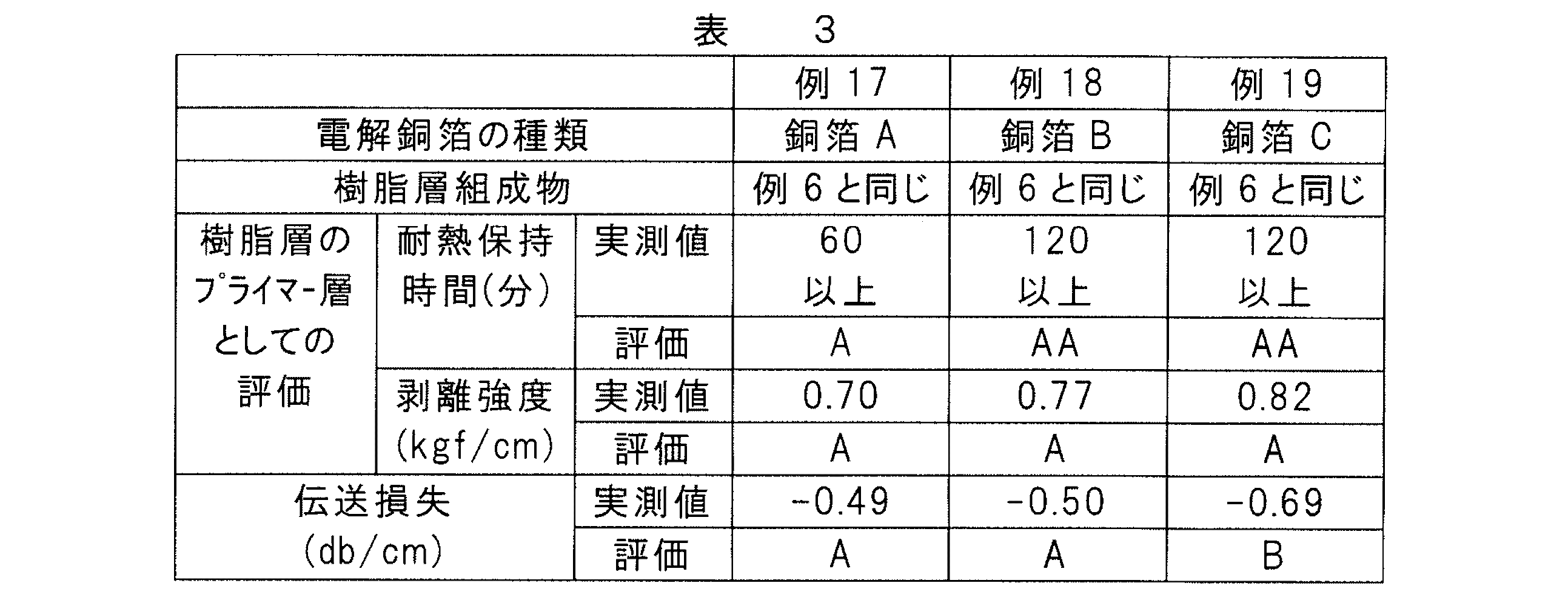
- a double-sided copper clad laminate 28 having a thickness of 0.14 mm was prepared by laminating together with two prepregs (MEGTRON-6 manufactured by Panasonic Corporation, actual thickness 68 ⁇ m) using the resin-coated copper foil 20 as the outermost layer. Then, the microstrip circuit was produced by carrying out pattern etching of copper foil. A pattern with a characteristic impedance of 50 ⁇ was selected, and a transmission loss S21 (db / cm) at 50 GHz was measured. The results were as shown in Table 3. -Evaluation A: -0.55 db / cm or more (good) -Evaluation B: -0.70db / cm or more (acceptable)
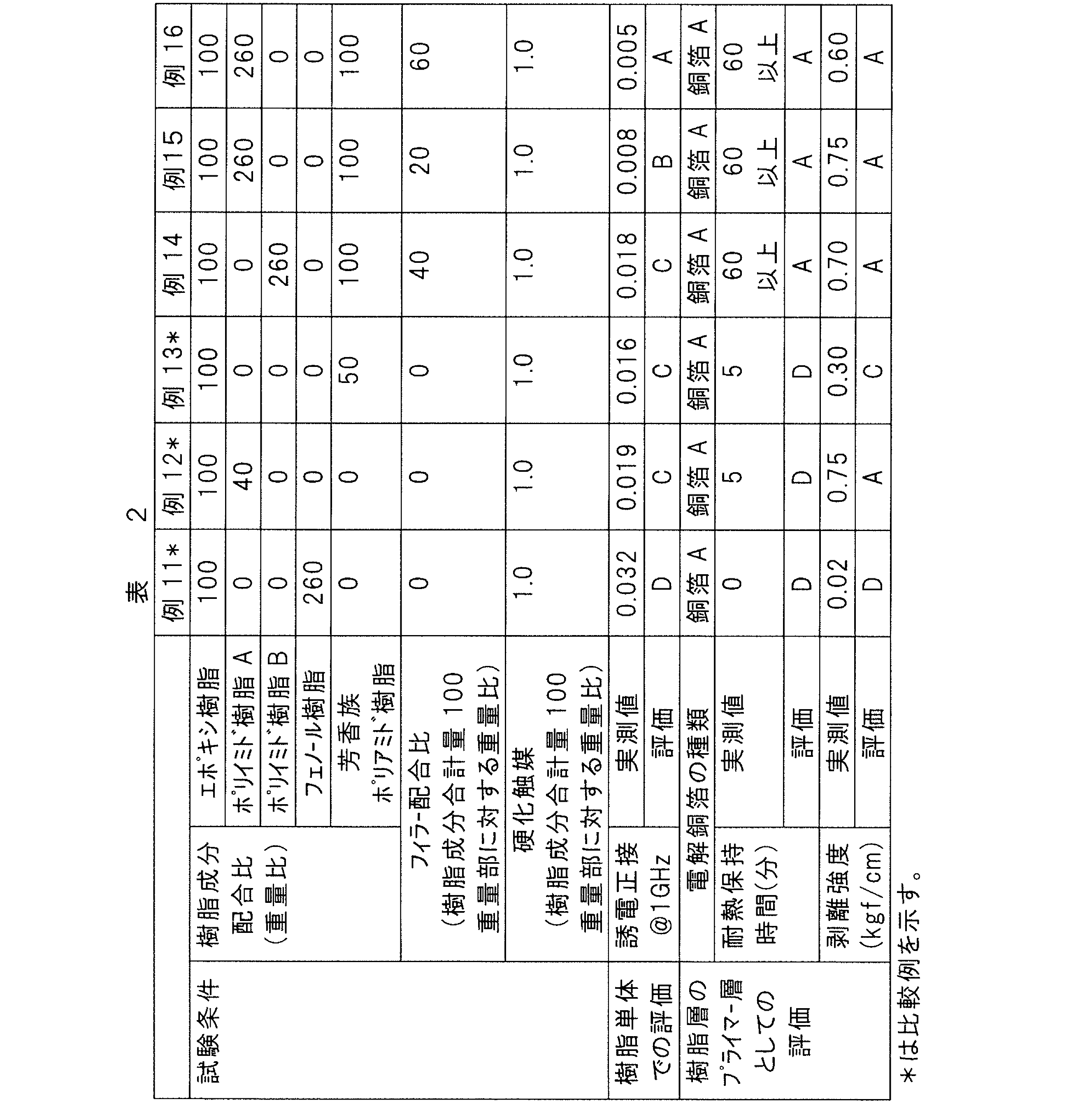
- Example 11 (Comparison) A resin varnish was prepared and evaluated in the same manner as in Example 10 except that a phenol resin (MEH-7500, manufactured by Meiwa Kasei Co., Ltd.) was used instead of the polyimide resin. The results were as shown in Table 2.
- Example 12 (Comparison) In the same manner as in Example 1 except that the blending ratio of the polyimide resin was reduced to 40 parts by weight (with respect to 100 parts by weight of the epoxy resin) and no aromatic polyamide resin was added, Various evaluations were performed. The results were as shown in Table 2.
- Example 13 (Comparison) In the same manner as in Example 1, except that the polyimide resin was not added and the blending ratio of the aromatic polyamide resin was reduced to 50 parts by weight (based on 100 parts by weight of the epoxy resin) Various evaluations were performed. The results were as shown in Table 2.
Landscapes
- Engineering & Computer Science (AREA)
- Microelectronics & Electronic Packaging (AREA)
- Manufacturing & Machinery (AREA)
- Ceramic Engineering (AREA)
- Textile Engineering (AREA)
- Chemical & Material Sciences (AREA)
- Laminated Bodies (AREA)
- Manufacturing Of Printed Wiring (AREA)
Abstract
Description
本発明の樹脂付銅箔は、銅箔の少なくとも片面に樹脂層を備えた樹脂付銅箔である。樹脂付銅箔は、樹脂層が、樹脂混合物と、イミダゾール系硬化触媒とを含む。この樹脂混合物はエポキシ樹脂、ポリイミド樹脂、及び芳香族ポリアミド樹脂を含む。このように、エポキシ樹脂、ポリイミド樹脂及び芳香族ポリアミド樹脂を、イミダゾール系硬化触媒と共に含む樹脂層を採用することで、樹脂層が高周波用途に適した優れた誘電特性(低い誘電正接)を有しながらも、銅張積層板又はプリント配線板とされた場合に、優れた層間密着性及び耐熱性を発揮させることができる。このような銅箔及び樹脂層間での優れた密着性及び耐熱性は、銅張積層板又はプリント配線板の製造に用いられた際に、回路剥がれ等の不具合を防止して製品歩留まりの向上を実現することができる。また、低い誘電正接は誘電体損失の低下に寄与し、その結果、高周波用途における伝送損失の低下を実現することができる。したがって、本発明の樹脂付銅箔は、ネットワーク機器における高周波デジタル通信用のプリント配線板用の絶縁層及び導体層として好ましく適用可能である。そのようなネットワーク機器の例としては、(i)基地局内サーバー、ルーター等、(ii)企業内ネットワーク、(iii)高速携帯通信の基幹システム等が挙げられる。
本発明の樹脂付銅箔はプリント配線板用銅張積層板の作製に用いられるのが好ましい。すなわち、本発明の好ましい態様によれば、上記樹脂付銅箔を備えた銅張積層板、又は上記樹脂付銅箔用いて得られた銅張積層板が提供される。この場合、上記樹脂付銅箔の樹脂層は硬化されている。この銅張積層板は、本発明の樹脂付銅箔と、この樹脂付銅箔の樹脂層に密着して設けられる絶縁基材層とを備えてなる。この場合、樹脂層は絶縁基材層との密着性を向上させるためのプライマー層として機能しうる。樹脂付銅箔は絶縁樹脂層の片面に設けられてもよいし、両面に設けられてもよい。絶縁樹脂層は、絶縁性樹脂を含んでなる。絶縁基材層は、ガラス繊維入りプリプレグ、ガラス板、セラミック板、樹脂フィルム、又はそれらの組合せであるのが好ましい。プリプレグとして用いる絶縁性樹脂の好ましい例としては、エポキシ樹脂、シアネートエステル樹脂、ポリイミド樹脂、ビスマレイミドトリアジン樹脂(BT樹脂)、ポリフェニレンエーテル樹脂、フェノール樹脂等が挙げられる。樹脂層は複数の層で構成されていてよい。この中でも、ポリフェニレンエーテル樹脂及びポリイミド樹脂は銅張積層板の伝送特性を向上される意味でも好ましく、本発明の樹脂付銅箔における樹脂層との密着性が特に優れるものとなる。樹脂フィルムとして用いる絶縁樹脂の例としては、ポリイミド樹脂、液晶ポリマー等が挙げられる。なお、銅張積層板を形成するための方法は各種考えられるが、典型的には本発明の樹脂付銅箔を絶縁基材層に張り合わせる方法で形成されるものである。その他には、絶縁基材層に樹脂層を先に塗布した後に、銅箔を樹脂層の表面に張り合わせ、絶縁基材層及び樹脂層を硬化させる方法も考えられる。言い換えれば、事後的に樹脂付金属箔としての層構成が備わった形態も、本発明の一つの形態に含まれるものとする。
本発明の樹脂付銅箔はプリント配線板の作製に用いられるのが好ましい。すなわち、本発明の好ましい態様によれば、上記樹脂付銅箔を備えたプリント配線板、又は上記樹脂付銅箔を用いて得られたプリント配線板が提供される。この場合、上記樹脂付銅箔の樹脂層は硬化されている。本態様によるプリント配線板は、絶縁樹脂層と、銅層とがこの順に積層された層構成を含んでなる。また、絶縁樹脂層については銅張積層板に関して上述したとおりである。いずれにしても、プリント配線板は公知の層構成が採用可能である。プリント配線板に関する具体例としては、プリプレグの片面又は両面に本発明の樹脂付銅箔を接着させ硬化した積層体とした上で回路形成した片面又は両面プリント配線板や、これらを多層化した多層プリント配線板等が挙げられる。また、他の具体例としては、樹脂フィルム上に本発明の樹脂付銅箔を形成して回路を形成するフレキシブルプリント配線板、COF、TABテープ、ビルドアップ多層配線板、半導体集積回路上へ樹脂付銅箔の積層と回路形成を交互に繰りかえすダイレクト・ビルドアップ・オン・ウェハー等が挙げられる。特に、本発明の樹脂付銅箔は、ネットワーク機器における高周波デジタル通信用のプリント配線板用の絶縁層及び導体層として好ましく適用可能である。そのようなネットワーク機器の例としては、(i)基地局内サーバー、ルーター等、(ii)企業内ネットワーク、(iii)高速携帯通信の基幹システム等が挙げられる。
樹脂組成物を含んでなる樹脂ワニスを調製し、この樹脂ワニスを用いて樹脂付銅箔を製造し、その評価を行った。具体的には以下のとおりである。
まず、樹脂ワニス用原料成分として、以下に示される樹脂成分、イミダゾール系硬化触媒及び無機フィラーを用意した。なお、無機フィラーは例6でのみ使用した。
‐ エポキシ樹脂:新日鉄住金化学株式会社製、YDCN-704(クレゾールノボラック型、エポキシ当量210g/Eq)
‐ ポリイミド樹脂A:荒川化学工業株式会社製、PIAD-300(末端官能基:カルボキシル基、溶媒:シクロヘキサノン、メチルシクロヘキサン及びエチレングルコールジメチルエーテルの混合液、誘電率(1GHz):2.70、誘電正接(1GHz):0.003、軟化点:140℃)
‐ ポリイミド樹脂B:株式会社T&K TOKA製、PI-2の溶剤希釈物(末端官能基:カルボキシル基、主溶媒:ジメチルアセトアミド、誘電率(1GHz):3.0、誘電正接(1GHz):0.018、軟化点:150℃)
‐ 芳香族ポリアミド樹脂:日本化薬株式会社製、BPAM-155(フェノール性水酸基含有ゴム変性型、水酸基当量4000g/Eq)
‐ イミダゾール系硬化触媒:四国化成工業株式会社製、2P4MHZ
‐ 無機フィラー:球状シリカ、アドマテックス株式会社製、SC1050-DJA(平均粒径D50=0.3μm、表面アミノシラン処理品)
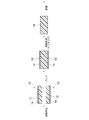
上記(1)で得られた樹脂ワニスを、厚さ18μmの電解銅箔の電極面(十点平均粗さRzjis:0.5μm、JIS B0601-2001に準拠して測定)に、乾燥後塗工厚みを50μmの厚さに狙って塗工した。塗工した樹脂ワニスをオーブンで乾燥させ、半硬化(Bステージ)状態とした。こうして図1に示されるように銅箔12の片面に樹脂層14を備えた樹脂付銅箔10を2枚作製した。図1に示されるように、2枚の樹脂付銅箔10を樹脂層14同士が重なるように積層して、プレス温度190℃、温度保持時間90分、プレス圧力40kgf/cm2の条件で真空プレスを行い、樹脂層14を硬化状態とした。こうして硬化された樹脂層14の厚さは100μmであった。プレス後の積層体から銅箔をエッチングして除去し、樹脂層14単独からなる樹脂フィルムを得た。
上記得られた樹脂フィルムについて、ネットワークアナライザー(キーサイト社製、PNA-L N5234A)を用いて空洞共振器摂動法により、1GHzにおける誘電正接を測定した。この測定はASTMD2520(JISC2565)に準拠して行った。得られた誘電正接を以下の基準に従い、4段階で評価した。
‐ 評価A:0.008未満(非常に良い)
‐ 評価B:0.008以上0.015未満(良い)
‐ 評価C:0.015以上0.020未満(許容可能)
‐ 評価D:0.020以上(悪い)
(3-1)電解銅箔の作製
厚さを18μmの電解銅箔A~Cをそれぞれ以下の方法により作製した。
硫酸銅溶液中で、陰極にチタン製の回転電極(表面粗さRa=0.20μm)を、陽極にDSAを用い、溶液温度45℃、電流密度55A/dm2で電解し、原箔を作製した。この硫酸銅溶液の組成は、銅濃度80g/L、フリー硫酸濃度140g/L、ビス(3-スルホプロピル)ジスルフィド濃度30mg/L、ジアリルジメチルアンモニウムクロライド重合体濃度50mg/L、塩素濃度40mg/Lとした。その後、原箔の電解液面に対して下記(a)~(c)の表面処理を順次行った。
(a)亜鉛-ニッケル被膜形成
‐ ピロリン酸カリウム濃度:80g/L
‐ 亜鉛濃度:0.2g/L、
‐ ニッケル濃度:2g/L
‐ 液温:40℃
‐ 電流密度:0.5A/dm2
(b)クロメート層形成
‐ クロム酸濃度:1g/L、pH11
‐ 溶液温度:25℃
‐ 電流密度:1A/dm2
(c)シラン層形成
‐ シランカップリング剤:3-アミノプロピルトリメトキシシラン(3g/L水溶液)
‐ 液処理方法:シャワー処理
こうして得られた電解銅箔Aの表面処理面は、十点平均粗さRzjisが0.5μm(JIS B0601-2001に準拠して測定)であり、粒子状突起は無いものであった。
電解銅箔Aの原箔の電解液面側の表面に粒子状突起を形成させ、その粒子状突起面に対して電解銅箔Aと同様の表面処理を行った。粒子突起は、硫酸銅溶液(銅濃度:13g/L、フリー硫酸濃度55g/L、9-フェニルアクリジン濃度140mg/L、塩素濃度35mg/L)中で、溶液温度30℃、電流密度50A/dm2の条件で電解することにより形成した。この電解銅箔Bの表面処理面は、十点平均粗さRzjisが0.5μm(JIS B0601-2001準拠)であり、粒子状突起は、走査型電子顕微鏡画像による平均粒子径が100nmであり、粒子密度は205個/μm2であった。
電解銅箔Aの原箔の電解液面側の表面に、粒子状突起を形成させた後、電解銅箔Aと同様の表面処理を行った。粒子突起の形成は、以下の3段階の電解処理により行った。1段目の電解処理は、硫酸銅溶液(銅濃度:10.5g/L、フリー硫酸濃度:220g/L)中にて、溶液温度30℃、電流密度28A/dm2の条件で行った。2段目の電解処理は、硫酸銅溶液(銅濃度:10.5g/L、フリー硫酸濃度:220g/L)中にて、溶液温度30℃、電流密度16A/dm2の条件で行った。3段目の電解処理は、硫酸銅溶液(銅濃度:70g/L、フリー硫酸濃度:220g/L)中にて、溶液温度52℃、電流密度21A/dm2の条件で行った。こうして得られた電解銅箔Cの表面処理面は、十点平均粗さRzjisが1.8μm(JIS B0601-2001準拠)であり、粒子状突起は、走査型電子顕微鏡画像による平均粒子径が1.0μmであり、粒子密度は1個/μm2であった。
上記(1)で得られた樹脂ワニスを、上記で得られた各電解銅箔の表面処理面に、乾燥後塗工厚みを3.0μmの厚さに狙って塗工した。塗工した樹脂ワニスをオーブンで乾燥させ、半硬化(Bステージ)状態とすることで、銅箔22の片面に樹脂層24を備えた樹脂付銅箔20を作製した。
プリプレグ(パナソニック株式会社製MEGTRON-6)を2枚積層して厚さ0.2mmの樹脂基材26を得た。図2に示されるように、2枚の樹脂付銅箔20の樹脂層24側を樹脂基材26の両面に積層し、プレス温度190℃、温度保持時間120分、プレス圧力30kgf/cm2の条件で真空プレスを行い、樹脂層24を硬化状態として銅張積層板28を得た。こうして硬化された樹脂層24の厚さは3.0μmであった。なお、樹脂層24は、銅張積層板28の作製において、樹脂基材26と接合するためのプライマー層として機能するといえる。得られた銅張積層板28に耐熱性評価用の基板作製を行った。具体的には、銅張積層板28を6.35mm×6.35mm平方に切り出した。熱機械分析装置(TMA)を用いて288℃に加熱された石英プローブを、切り出した銅張積層板28の表面に接触させて、デラミネーション(回路剥離や基材剥離)が発生するまでの時間(分)を測定した。この測定はIPC-TM-650(No.2.4.24.1)に準拠して行った。結果は表1~3に示されるとおりであった。
‐ 評価AA:120分以上(極上に良い)
‐ 評価A:60分以上(非常に良い)
‐ 評価B:30分以上60分未満(良い)
‐ 評価C:10分以上30分未満(許容可能)
‐ 評価D:10分未満(悪い)
上記得られた銅張積層板28に剥離強度測定試験用の回路形成を行った。具体的には、銅張積層板28の両面にドライフィルムを張り合わせて、エッチングレジスト層を形成した。そして、その両面のエッチングレジスト層に、10mm幅の剥離強度測定試験用の回路を露光現像し、エッチングパターンを形成した。その後、銅エッチング液で回路エッチングを行い、エッチングレジストを剥離して回路22aを得た。こうして形成された回路22aを樹脂層24から剥離して、回路22a及び樹脂層24間の剥離強度(kgf/cm)を測定した。この剥離強度の測定はJIS C 6481-1996に準拠して行った。結果は表1~3に示されるとおりであった。
‐ 評価A:0.60kgf/cm以上(非常に良い)
‐ 評価B:0.40kgf/cm以上0.60kgf/cm未満(良い)
‐ 評価C:0.20kgf/cm以上0.40kgf/cm未満(許容可能)
‐ 評価D:0.20kgf/cm未満(悪い)
樹脂付銅箔20を最外層として、2枚のプリプレグ(パナソニック株式会社製MEGTRON-6、実厚さ68μm)と共に積層して、厚さ0.14mmの両面銅張積層板28を作製した。その後、銅箔をパターンエッチングすることにより、マイクロストリップ回路を作製した。回路の特性インピーダンスが50Ωとなるパターンを選定し、50GHzにおける伝送損失S21(db/cm)を測定した。結果は表3に示されるとおりであった。
‐ 評価A:-0.55db/cm以上(良い)
‐ 評価B:-0.70db/cm以上(許容可能)
ポリイミド樹脂の代わりにフェノール樹脂(明和化成株式会社製、MEH-7500)を用いたこと以外は例10と同様にして、樹脂ワニスの調製及び各種評価を行った。結果は表2に示されるとおりであった。
ポリイミド樹脂の配合比を40重量部(エポキシ樹脂100重量部に対して)に減らしたこと、及び芳香族ポリアミド樹脂を添加しなかったこと以外は、例1と同様にして、樹脂ワニスの調製及び各種評価を行った。結果は表2に示されるとおりであった。
ポリイミド樹脂を添加しなかったこと、及び芳香族ポリアミド樹脂の配合比を50重量部(エポキシ樹脂100重量部に対して)に減らしたこと以外は、例1と同様にして、樹脂ワニスの調製及び各種評価を行った。結果は表2に示されるとおりであった。

Claims (14)
- 銅箔の少なくとも片面に樹脂層を備えた樹脂付銅箔であって、前記樹脂層が、
エポキシ樹脂、ポリイミド樹脂、及び芳香族ポリアミド樹脂を含む樹脂混合物と、
イミダゾール系硬化触媒と、
を含む、樹脂付銅箔。 - 前記樹脂混合物が、前記エポキシ樹脂100重量部に対して、前記ポリイミド樹脂を160~340重量部を含み、かつ、前記芳香族ポリアミド樹脂を50~200重量部含む、請求項1に記載の樹脂付銅箔。
- 前記樹脂混合物が、前記エポキシ樹脂100重量部に対して、前記ポリイミド樹脂を200~300重量部を含み、かつ、前記芳香族ポリアミド樹脂を80~150重量部含む、請求項1に記載の樹脂付銅箔。
- 前記樹脂層が無機フィラーをさらに含む、請求項1~3のいずれか一項に記載の樹脂付銅箔。
- 前記ポリイミド樹脂が、ポリイミド樹脂単体として、周波数1GHzにおいて、誘電率が2.0~3.0、誘電正接が0.001~0.005である、請求項1~4のいずれか一項に記載の樹脂付銅箔。
- 前記樹脂層が、前記エポキシ樹脂、前記ポリイミド樹脂、及び前記芳香族ポリアミド樹脂の合計量100重量部に対して、前記無機フィラーを10~100重量部含む、請求項1~4のいずれか一項に記載の樹脂付銅箔。
- 前記無機フィラーがシリカ粒子である、請求項4~6のいずれか一項に記載の樹脂付銅箔。
- 前記銅箔の樹脂層側の表面における、JIS B0601-2001に準拠して測定される十点平均粗さRzjisが2.0μm以下である、請求項1~7のいずれか一項に記載の樹脂付銅箔。
- 前記銅箔の樹脂層側の表面に、平均粒径10~300nmの粒子状突起を備えた、請求項1~8のいずれか一項に記載の樹脂付銅箔。
- 前記銅箔の樹脂層側の表面に、粒子状突起が40~280個/μm2で存在する、請求項1~9のいずれか一項に記載の樹脂付銅箔。
- 前記樹脂層が硬化された状態において、前記樹脂層が、周波数1GHzにおいて、0.020未満の誘電正接を有する、請求項1~10のいずれか一項に記載の樹脂付銅箔。
- 前記樹脂層が硬化された状態において、JIS C6481-1996に準拠して測定される、前記樹脂層及び前記銅箔間の剥離強度が0.40kgf/cm以上である、請求項1~11のいずれか一項に記載の樹脂付銅箔。
- 請求項1~12のいずれか一項に記載の樹脂付銅箔を備えてなり、前記樹脂層が硬化されている、銅張積層板。
- 請求項1~12のいずれか一項に記載の樹脂付銅箔を備えてなり、前記樹脂層が硬化されている、プリント配線板。
Priority Applications (4)
| Application Number | Priority Date | Filing Date | Title |
|---|---|---|---|
| KR1020187001456A KR102070047B1 (ko) | 2015-07-23 | 2016-07-08 | 수지 부착 구리박, 동장 적층판 및 프린트 배선판 |
| CN201680043034.6A CN107848260B (zh) | 2015-07-23 | 2016-07-08 | 带树脂的铜箔、覆铜层叠板和印刷电路板 |
| JP2017529553A JP6426290B2 (ja) | 2015-07-23 | 2016-07-08 | 樹脂付銅箔、銅張積層板及びプリント配線板 |
| US15/743,466 US11166383B2 (en) | 2015-07-23 | 2016-07-08 | Resin-clad copper foil, copper-clad laminated plate, and printed wiring board |
Applications Claiming Priority (2)
| Application Number | Priority Date | Filing Date | Title |
|---|---|---|---|
| JP2015-146158 | 2015-07-23 | ||
| JP2015146158 | 2015-07-23 |
Publications (1)
| Publication Number | Publication Date |
|---|---|
| WO2017014079A1 true WO2017014079A1 (ja) | 2017-01-26 |
Family
ID=57833983
Family Applications (1)
| Application Number | Title | Priority Date | Filing Date |
|---|---|---|---|
| PCT/JP2016/070332 Ceased WO2017014079A1 (ja) | 2015-07-23 | 2016-07-08 | 樹脂付銅箔、銅張積層板及びプリント配線板 |
Country Status (7)
| Country | Link |
|---|---|
| US (1) | US11166383B2 (ja) |
| JP (1) | JP6426290B2 (ja) |
| KR (1) | KR102070047B1 (ja) |
| CN (1) | CN107848260B (ja) |
| MY (1) | MY180785A (ja) |
| TW (1) | TWI609043B (ja) |
| WO (1) | WO2017014079A1 (ja) |
Cited By (2)
| Publication number | Priority date | Publication date | Assignee | Title |
|---|---|---|---|---|
| KR20210052283A (ko) | 2019-10-29 | 2021-05-10 | 닛테츠 케미컬 앤드 머티리얼 가부시키가이샤 | 수지 조성물, 수지 필름 및 금속 피복 적층판 |
| JP2023068801A (ja) * | 2021-11-04 | 2023-05-18 | 日本化薬株式会社 | ポリイミド樹脂組成物及びその硬化物 |
Families Citing this family (12)
| Publication number | Priority date | Publication date | Assignee | Title |
|---|---|---|---|---|
| EP3480843B1 (en) * | 2016-07-01 | 2021-05-05 | Mitsubishi Gas Chemical Company, Inc. | Method for manufacturing package substrate for carrying semiconductor element, and method for manufacturing semiconductor element-mounted substrate |
| CN106190004B (zh) * | 2016-07-20 | 2020-05-15 | 律胜科技(苏州)有限公司 | 一种具有高频特性的接着剂组合物及其用途 |
| JP6553311B2 (ja) | 2017-01-10 | 2019-07-31 | 住友精化株式会社 | エポキシ樹脂組成物 |
| JP7057689B2 (ja) * | 2018-03-16 | 2022-04-20 | 日本ピラー工業株式会社 | 積層板 |
| CN109535700A (zh) * | 2018-11-13 | 2019-03-29 | 四川塑金科技有限公司 | 再生热塑性材料及其制备方法和应用 |
| WO2021079819A1 (ja) * | 2019-10-25 | 2021-04-29 | パナソニックIpマネジメント株式会社 | 銅張積層板、配線板、及び樹脂付き銅箔 |
| US20230128897A1 (en) * | 2020-01-16 | 2023-04-27 | Sumitomo Seika Chemicals Co., Ltd. | Laminated body having copper foil and epoxy resin composition layer |
| US11342254B2 (en) * | 2020-03-16 | 2022-05-24 | Qualcomm Incorporated | Multi-dielectric structure in two-layer embedded trace substrate |
| KR102413300B1 (ko) | 2020-12-10 | 2022-06-27 | 와이엠티 주식회사 | 금속박, 이를 포함하는 캐리어 부착 금속박 및 이를 포함하는 인쇄회로기판 |
| KR102454686B1 (ko) * | 2020-12-30 | 2022-10-13 | 에스케이씨 주식회사 | 표면 처리 동박 및 이를 포함하는 회로 기판 |
| US20250046520A1 (en) * | 2021-10-28 | 2025-02-06 | Mitsui Mining & Smelting Co., Ltd. | Double-sided copper clad laminate, capacitor element and printed wiring board with built-in capacitor, and method for manufacturing double-sided copper clad laminate |
| KR102840704B1 (ko) | 2022-06-09 | 2025-07-31 | 와이엠티 주식회사 | 금속층, 이를 포함하는 캐리어 부착 금속박 및 이를 포함하는 인쇄회로기판 |
Citations (6)
| Publication number | Priority date | Publication date | Assignee | Title |
|---|---|---|---|---|
| JP2006131690A (ja) * | 2004-11-02 | 2006-05-25 | Kaneka Corp | 樹脂組成物の流動性を向上させる樹脂改質材およびその利用 |
| JP2006328214A (ja) * | 2005-05-26 | 2006-12-07 | Tamura Kaken Co Ltd | 熱硬化性樹脂組成物、樹脂フィルムおよびフィルム付き製品 |
| JP2008284785A (ja) * | 2007-05-17 | 2008-11-27 | Nippon Kayaku Co Ltd | 樹脂層付き銅箔 |
| JP2009148962A (ja) * | 2007-12-19 | 2009-07-09 | Mitsui Mining & Smelting Co Ltd | フィラー粒子含有樹脂層付銅箔及びそのフィラー粒子含有樹脂層付銅箔を用いた銅張積層板 |
| WO2009145207A1 (ja) * | 2008-05-28 | 2009-12-03 | 三井金属鉱業株式会社 | 銅箔の粗化処理方法及びその粗化処理方法で得られるプリント配線板用銅箔 |
| JP2015091644A (ja) * | 2013-09-30 | 2015-05-14 | 新日鉄住金化学株式会社 | 銅張積層板、プリント配線板及びその使用方法 |
Family Cites Families (11)
| Publication number | Priority date | Publication date | Assignee | Title |
|---|---|---|---|---|
| JPS5118469A (en) | 1974-08-07 | 1976-02-14 | Fujitsu Ltd | Gasuhodensoshino seizoho |
| US4377652A (en) * | 1978-02-17 | 1983-03-22 | Asahi Kasei Kogyo Kabushiki Kaisha | Polyamide-imide compositions and articles for electrical use prepared therefrom |
| JP3157562B2 (ja) | 1991-10-28 | 2001-04-16 | 日本碍子株式会社 | 多機能濾過機に使用するバルブ |
| JP3949676B2 (ja) | 2003-07-22 | 2007-07-25 | 三井金属鉱業株式会社 | 極薄接着剤層付銅箔及びその極薄接着剤層付銅箔の製造方法 |
| WO2005080466A1 (ja) * | 2004-02-25 | 2005-09-01 | Kaneka Corporation | 熱硬化性樹脂組成物およびその利用 |
| JP5019874B2 (ja) * | 2004-04-19 | 2012-09-05 | 株式会社カネカ | 熱硬化性樹脂組成物、及びそれを用いてなる積層体、回路基板 |
| JP2006274248A (ja) * | 2005-03-03 | 2006-10-12 | Toray Ind Inc | 半導体装置用接着剤付きテープおよびその製造方法、それを用いたパターン加工テープ |
| CN101679612B (zh) * | 2007-06-14 | 2013-07-17 | 味之素株式会社 | 多层印刷电路板的层间绝缘用树脂组合物 |
| JP5304954B2 (ja) * | 2011-05-31 | 2013-10-02 | 東洋紡株式会社 | カルボキシル基含有ポリイミド |
| WO2013105650A1 (ja) | 2012-01-11 | 2013-07-18 | 三井金属鉱業株式会社 | 接着剤層付銅箔、銅張積層板及びプリント配線板 |
| JP5156873B1 (ja) | 2012-07-25 | 2013-03-06 | Jx日鉱日石金属株式会社 | キャリア付銅箔 |
-
2016
- 2016-07-08 JP JP2017529553A patent/JP6426290B2/ja active Active
- 2016-07-08 MY MYPI2018700089A patent/MY180785A/en unknown
- 2016-07-08 CN CN201680043034.6A patent/CN107848260B/zh active Active
- 2016-07-08 WO PCT/JP2016/070332 patent/WO2017014079A1/ja not_active Ceased
- 2016-07-08 US US15/743,466 patent/US11166383B2/en not_active Expired - Fee Related
- 2016-07-08 KR KR1020187001456A patent/KR102070047B1/ko active Active
- 2016-07-15 TW TW105122437A patent/TWI609043B/zh active
Patent Citations (6)
| Publication number | Priority date | Publication date | Assignee | Title |
|---|---|---|---|---|
| JP2006131690A (ja) * | 2004-11-02 | 2006-05-25 | Kaneka Corp | 樹脂組成物の流動性を向上させる樹脂改質材およびその利用 |
| JP2006328214A (ja) * | 2005-05-26 | 2006-12-07 | Tamura Kaken Co Ltd | 熱硬化性樹脂組成物、樹脂フィルムおよびフィルム付き製品 |
| JP2008284785A (ja) * | 2007-05-17 | 2008-11-27 | Nippon Kayaku Co Ltd | 樹脂層付き銅箔 |
| JP2009148962A (ja) * | 2007-12-19 | 2009-07-09 | Mitsui Mining & Smelting Co Ltd | フィラー粒子含有樹脂層付銅箔及びそのフィラー粒子含有樹脂層付銅箔を用いた銅張積層板 |
| WO2009145207A1 (ja) * | 2008-05-28 | 2009-12-03 | 三井金属鉱業株式会社 | 銅箔の粗化処理方法及びその粗化処理方法で得られるプリント配線板用銅箔 |
| JP2015091644A (ja) * | 2013-09-30 | 2015-05-14 | 新日鉄住金化学株式会社 | 銅張積層板、プリント配線板及びその使用方法 |
Cited By (2)
| Publication number | Priority date | Publication date | Assignee | Title |
|---|---|---|---|---|
| KR20210052283A (ko) | 2019-10-29 | 2021-05-10 | 닛테츠 케미컬 앤드 머티리얼 가부시키가이샤 | 수지 조성물, 수지 필름 및 금속 피복 적층판 |
| JP2023068801A (ja) * | 2021-11-04 | 2023-05-18 | 日本化薬株式会社 | ポリイミド樹脂組成物及びその硬化物 |
Also Published As
| Publication number | Publication date |
|---|---|
| CN107848260B (zh) | 2020-10-30 |
| US20180206345A1 (en) | 2018-07-19 |
| CN107848260A (zh) | 2018-03-27 |
| KR102070047B1 (ko) | 2020-01-29 |
| KR20180019190A (ko) | 2018-02-23 |
| JPWO2017014079A1 (ja) | 2018-01-25 |
| JP6426290B2 (ja) | 2018-11-21 |
| TW201716500A (zh) | 2017-05-16 |
| US11166383B2 (en) | 2021-11-02 |
| TWI609043B (zh) | 2017-12-21 |
| MY180785A (en) | 2020-12-09 |
Similar Documents
| Publication | Publication Date | Title |
|---|---|---|
| JP6426290B2 (ja) | 樹脂付銅箔、銅張積層板及びプリント配線板 | |
| JP7212626B2 (ja) | プリント配線板用樹脂組成物、樹脂付銅箔、銅張積層板、及びプリント配線板 | |
| CN111836716B (zh) | 覆铜层叠板 | |
| TWI696661B (zh) | 熱硬化性樹脂組成物、層間絕緣用樹脂薄膜、複合薄膜、印刷線路板及其製造方法 | |
| CN102574365B (zh) | 树脂复合电解铜箔、覆铜层压板和印刷线路板 | |
| TWI637852B (zh) | Resin sheet with support | |
| CN104584699B (zh) | 附载体铜箔 | |
| WO2005009093A1 (ja) | 極薄接着剤層付銅箔及びその極薄接着剤層付銅箔の製造方法 | |
| CN104098871A (zh) | 固化性树脂组合物 | |
| CN101484513A (zh) | 聚酰亚胺树脂层的表面改性方法以及覆金属层合板的制造方法 | |
| CN104822525A (zh) | 附载体铜箔 | |
| CN104822524A (zh) | 附载体铜箔 | |
| CN104685109B (zh) | 附载体的铜箔及用有附载体的铜箔的覆铜积层板 | |
| CN111995832B (zh) | 树脂组合物、胶黏剂及柔性覆铜板 | |
| JP6295708B2 (ja) | 樹脂組成物、めっきプロセス用プライマー層、支持体付きめっきプロセス用プライマー層、硬化後めっきプロセス用プライマー層、配線板用積層板、配線板用積層板の製造方法、多層配線板、及び多層配線板の製造方法 | |
| WO2018199003A1 (ja) | 支持体及びそれを用いた半導体素子実装基板の製造方法 | |
| TWI859358B (zh) | 樹脂組成物及附樹脂銅箔 | |
| JP2017035843A (ja) | 接着層付き金属箔、これを用いた金属張積層板および多層プリント配線板 |
Legal Events
| Date | Code | Title | Description |
|---|---|---|---|
| 121 | Ep: the epo has been informed by wipo that ep was designated in this application |
Ref document number: 16827641 Country of ref document: EP Kind code of ref document: A1 |
|
| ENP | Entry into the national phase |
Ref document number: 2017529553 Country of ref document: JP Kind code of ref document: A |
|
| WWE | Wipo information: entry into national phase |
Ref document number: 15743466 Country of ref document: US |
|
| ENP | Entry into the national phase |
Ref document number: 20187001456 Country of ref document: KR Kind code of ref document: A |
|
| NENP | Non-entry into the national phase |
Ref country code: DE |
|
| 122 | Ep: pct application non-entry in european phase |
Ref document number: 16827641 Country of ref document: EP Kind code of ref document: A1 |