WO2017013988A1 - ウェットエッチング方法及びエッチング液 - Google Patents
ウェットエッチング方法及びエッチング液 Download PDFInfo
- Publication number
- WO2017013988A1 WO2017013988A1 PCT/JP2016/068456 JP2016068456W WO2017013988A1 WO 2017013988 A1 WO2017013988 A1 WO 2017013988A1 JP 2016068456 W JP2016068456 W JP 2016068456W WO 2017013988 A1 WO2017013988 A1 WO 2017013988A1
- Authority
- WO
- WIPO (PCT)
- Prior art keywords
- wet etching
- metal
- etching solution
- diketone
- etching method
- Prior art date
- Legal status (The legal status is an assumption and is not a legal conclusion. Google has not performed a legal analysis and makes no representation as to the accuracy of the status listed.)
- Ceased
Links
Classifications
-
- C—CHEMISTRY; METALLURGY
- C23—COATING METALLIC MATERIAL; COATING MATERIAL WITH METALLIC MATERIAL; CHEMICAL SURFACE TREATMENT; DIFFUSION TREATMENT OF METALLIC MATERIAL; COATING BY VACUUM EVAPORATION, BY SPUTTERING, BY ION IMPLANTATION OR BY CHEMICAL VAPOUR DEPOSITION, IN GENERAL; INHIBITING CORROSION OF METALLIC MATERIAL OR INCRUSTATION IN GENERAL
- C23F—NON-MECHANICAL REMOVAL OF METALLIC MATERIAL FROM SURFACE; INHIBITING CORROSION OF METALLIC MATERIAL OR INCRUSTATION IN GENERAL; MULTI-STEP PROCESSES FOR SURFACE TREATMENT OF METALLIC MATERIAL INVOLVING AT LEAST ONE PROCESS PROVIDED FOR IN CLASS C23 AND AT LEAST ONE PROCESS COVERED BY SUBCLASS C21D OR C22F OR CLASS C25
- C23F1/00—Etching metallic material by chemical means
- C23F1/02—Local etching
-
- C—CHEMISTRY; METALLURGY
- C23—COATING METALLIC MATERIAL; COATING MATERIAL WITH METALLIC MATERIAL; CHEMICAL SURFACE TREATMENT; DIFFUSION TREATMENT OF METALLIC MATERIAL; COATING BY VACUUM EVAPORATION, BY SPUTTERING, BY ION IMPLANTATION OR BY CHEMICAL VAPOUR DEPOSITION, IN GENERAL; INHIBITING CORROSION OF METALLIC MATERIAL OR INCRUSTATION IN GENERAL
- C23F—NON-MECHANICAL REMOVAL OF METALLIC MATERIAL FROM SURFACE; INHIBITING CORROSION OF METALLIC MATERIAL OR INCRUSTATION IN GENERAL; MULTI-STEP PROCESSES FOR SURFACE TREATMENT OF METALLIC MATERIAL INVOLVING AT LEAST ONE PROCESS PROVIDED FOR IN CLASS C23 AND AT LEAST ONE PROCESS COVERED BY SUBCLASS C21D OR C22F OR CLASS C25
- C23F1/00—Etching metallic material by chemical means
- C23F1/10—Etching compositions
-
- C—CHEMISTRY; METALLURGY
- C23—COATING METALLIC MATERIAL; COATING MATERIAL WITH METALLIC MATERIAL; CHEMICAL SURFACE TREATMENT; DIFFUSION TREATMENT OF METALLIC MATERIAL; COATING BY VACUUM EVAPORATION, BY SPUTTERING, BY ION IMPLANTATION OR BY CHEMICAL VAPOUR DEPOSITION, IN GENERAL; INHIBITING CORROSION OF METALLIC MATERIAL OR INCRUSTATION IN GENERAL
- C23F—NON-MECHANICAL REMOVAL OF METALLIC MATERIAL FROM SURFACE; INHIBITING CORROSION OF METALLIC MATERIAL OR INCRUSTATION IN GENERAL; MULTI-STEP PROCESSES FOR SURFACE TREATMENT OF METALLIC MATERIAL INVOLVING AT LEAST ONE PROCESS PROVIDED FOR IN CLASS C23 AND AT LEAST ONE PROCESS COVERED BY SUBCLASS C21D OR C22F OR CLASS C25
- C23F1/00—Etching metallic material by chemical means
- C23F1/10—Etching compositions
- C23F1/14—Aqueous compositions
-
- C—CHEMISTRY; METALLURGY
- C23—COATING METALLIC MATERIAL; COATING MATERIAL WITH METALLIC MATERIAL; CHEMICAL SURFACE TREATMENT; DIFFUSION TREATMENT OF METALLIC MATERIAL; COATING BY VACUUM EVAPORATION, BY SPUTTERING, BY ION IMPLANTATION OR BY CHEMICAL VAPOUR DEPOSITION, IN GENERAL; INHIBITING CORROSION OF METALLIC MATERIAL OR INCRUSTATION IN GENERAL
- C23F—NON-MECHANICAL REMOVAL OF METALLIC MATERIAL FROM SURFACE; INHIBITING CORROSION OF METALLIC MATERIAL OR INCRUSTATION IN GENERAL; MULTI-STEP PROCESSES FOR SURFACE TREATMENT OF METALLIC MATERIAL INVOLVING AT LEAST ONE PROCESS PROVIDED FOR IN CLASS C23 AND AT LEAST ONE PROCESS COVERED BY SUBCLASS C21D OR C22F OR CLASS C25
- C23F1/00—Etching metallic material by chemical means
- C23F1/44—Compositions for etching metallic material from a metallic material substrate of different composition
-
- H—ELECTRICITY
- H10—SEMICONDUCTOR DEVICES; ELECTRIC SOLID-STATE DEVICES NOT OTHERWISE PROVIDED FOR
- H10P—GENERIC PROCESSES OR APPARATUS FOR THE MANUFACTURE OR TREATMENT OF DEVICES COVERED BY CLASS H10
- H10P50/00—Etching of wafers, substrates or parts of devices
- H10P50/20—Dry etching; Plasma etching; Reactive-ion etching
- H10P50/28—Dry etching; Plasma etching; Reactive-ion etching of insulating materials
- H10P50/282—Dry etching; Plasma etching; Reactive-ion etching of insulating materials of inorganic materials
- H10P50/283—Dry etching; Plasma etching; Reactive-ion etching of insulating materials of inorganic materials by chemical means
-
- H—ELECTRICITY
- H10—SEMICONDUCTOR DEVICES; ELECTRIC SOLID-STATE DEVICES NOT OTHERWISE PROVIDED FOR
- H10P—GENERIC PROCESSES OR APPARATUS FOR THE MANUFACTURE OR TREATMENT OF DEVICES COVERED BY CLASS H10
- H10P50/00—Etching of wafers, substrates or parts of devices
- H10P50/60—Wet etching
- H10P50/64—Wet etching of semiconductor materials
- H10P50/642—Chemical etching
-
- H—ELECTRICITY
- H10—SEMICONDUCTOR DEVICES; ELECTRIC SOLID-STATE DEVICES NOT OTHERWISE PROVIDED FOR
- H10P—GENERIC PROCESSES OR APPARATUS FOR THE MANUFACTURE OR TREATMENT OF DEVICES COVERED BY CLASS H10
- H10P50/00—Etching of wafers, substrates or parts of devices
- H10P50/60—Wet etching
- H10P50/64—Wet etching of semiconductor materials
- H10P50/642—Chemical etching
- H10P50/646—Chemical etching of Group III-V materials
-
- H—ELECTRICITY
- H10—SEMICONDUCTOR DEVICES; ELECTRIC SOLID-STATE DEVICES NOT OTHERWISE PROVIDED FOR
- H10P—GENERIC PROCESSES OR APPARATUS FOR THE MANUFACTURE OR TREATMENT OF DEVICES COVERED BY CLASS H10
- H10P50/00—Etching of wafers, substrates or parts of devices
- H10P50/60—Wet etching
- H10P50/66—Wet etching of conductive or resistive materials
- H10P50/663—Wet etching of conductive or resistive materials by chemical means only
- H10P50/667—Wet etching of conductive or resistive materials by chemical means only by liquid etching only
-
- H—ELECTRICITY
- H10—SEMICONDUCTOR DEVICES; ELECTRIC SOLID-STATE DEVICES NOT OTHERWISE PROVIDED FOR
- H10P—GENERIC PROCESSES OR APPARATUS FOR THE MANUFACTURE OR TREATMENT OF DEVICES COVERED BY CLASS H10
- H10P50/00—Etching of wafers, substrates or parts of devices
- H10P50/69—Etching of wafers, substrates or parts of devices using masks for semiconductor materials
- H10P50/691—Etching of wafers, substrates or parts of devices using masks for semiconductor materials for Group V materials or Group III-V materials
-
- H—ELECTRICITY
- H10—SEMICONDUCTOR DEVICES; ELECTRIC SOLID-STATE DEVICES NOT OTHERWISE PROVIDED FOR
- H10N—ELECTRIC SOLID-STATE DEVICES NOT OTHERWISE PROVIDED FOR
- H10N50/00—Galvanomagnetic devices
- H10N50/01—Manufacture or treatment
-
- H—ELECTRICITY
- H10—SEMICONDUCTOR DEVICES; ELECTRIC SOLID-STATE DEVICES NOT OTHERWISE PROVIDED FOR
- H10N—ELECTRIC SOLID-STATE DEVICES NOT OTHERWISE PROVIDED FOR
- H10N70/00—Solid-state devices having no potential barriers, and specially adapted for rectifying, amplifying, oscillating or switching
- H10N70/011—Manufacture or treatment of multistable switching devices
- H10N70/061—Shaping switching materials
- H10N70/063—Shaping switching materials by etching of pre-deposited switching material layers, e.g. lithography
Definitions
- the present invention relates to a wet etching method and etching solution for a metal-containing film used in a semiconductor manufacturing process or the like.
- a metal-containing film such as a metal film as a metal gate material, an electrode material, or a magnetic material, or a metal compound film as a piezoelectric material, an LED light-emitting material, a transparent electrode material, or a dielectric material is used. Etching is performed to form a desired pattern.
- a dry etching method using ⁇ -diketone As a method for etching a metal-containing film, a dry etching method using ⁇ -diketone is known. For example, a method of forming a patterned metal film including a dry etching process in which a seed layer made of a transition metal is anisotropically oxidized and removed using a gas such as HFAc is disclosed (Patent Document 1). Also disclosed is a method of dry etching a metal film such as Co, Fe, Zn, Mn, Ni formed on a substrate using an etching gas containing ⁇ -diketone and H 2 O (Patent Document 2). ).
- Patent Documents 3 and 5 there is wet etching using a chemical solution.
- the wet etching in the manufacturing process of the semiconductor element uses an etching solution containing an inorganic acid, an organic acid, or an oxidizing substance (for example, Patent Documents 3, 4, and 5).
- wet etching is advantageous in that the cost of equipment and chemicals is low and a large number of substrates can be processed at one time.
- the conventional etching solution may react not only with the metal-containing film that is the object of etching but also with the substrate that is not the object of etching, which deteriorates the characteristics of the device incorporating the metal-containing film. was there.
- the present invention has been made in view of the above problems, and an object thereof is to provide a method for efficiently etching a metal-containing film on a substrate using an etching solution.
- the present inventors use an organic solvent solution of a ⁇ -diketone in which a trifluoromethyl group and a carbonyl group are bonded as an etching solution, the ⁇ -diketone forms a complex with a metal and can etch a metal-containing film on a substrate. And found the present invention.
- the first aspect of the present invention is a wet etching method in which a metal-containing film on a substrate is etched using an etchant, wherein the etchant is a ⁇ -bonded trifluoromethyl group and a carbonyl group.
- the wet etching method is a solution of a diketone and an organic solvent, wherein the metal-containing film contains a metal element capable of forming a complex with the ⁇ -diketone.
- the second aspect of the present invention includes at least one organic solvent selected from the group consisting of isopropyl alcohol, methanol, ethanol, propylene glycol monomethyl ether acetate (PGMEA), methyl ethyl ketone (MEK), and acetone, and trifluoro An etching solution comprising a methyl group and a ⁇ -diketone to which a carbonyl group is bonded.
- organic solvent selected from the group consisting of isopropyl alcohol, methanol, ethanol, propylene glycol monomethyl ether acetate (PGMEA), methyl ethyl ketone (MEK), and acetone
- wet etching method of metal-containing film In the wet etching method of the present invention, the metal-containing film on the substrate is etched using an etching solution containing ⁇ -diketone in which a trifluoromethyl group and a carbonyl group are bonded.
- the metal-containing film to be etched by the wet etching method of the present invention contains a metal element capable of forming a complex with the ⁇ -diketone.
- a metal element capable of forming a complex with the ⁇ -diketone.
- the metal element contained in the metal-containing film Ti, Zr, Hf, V, Nb, Ta, Cr, Mo, W, Mn, Re, Fe, Ru, Os, Co, Rh, Ir, Ni, Pd, Pt Cu, Ag, Au, Zn, Cd, Al, Ga, In, Sn, Pb, and As.
- These metals can form a complex with ⁇ -diketone, form a complex with ⁇ -diketone in the etching solution, and dissolve in the etching solution.
- metal element contained in the metal-containing film Ti, Zr, Hf, V, Cr, Mn, Fe, Ru, Os, Co, Rh, Ir, Ni, Pd, Pt, Cu, Zn, Al, Ga, In, Sn, Pb, and As are preferable, and Ti, Zr, Hf, Cr, Fe, Ru, Co, Ni, Pt, Cu, Zn, Al, Ga, In, Sn, and Pb are more preferable.
- the metal-containing film is preferably any one of a single film made of one kind of metal element, an alloy film containing the metal element, and a compound film containing the metal element. A film in which these metal-containing films are stacked may be etched.
- the alloy film containing a plurality of types of the above metal elements is not only an alloy film such as NiCo, CoFe, CoPt, MnZn, NiZn, CuZn, FeNi, but also an alloy film doped with other elements such as CoFeB. May be.
- the metal element compound film includes an intermetallic compound containing a plurality of the above metal elements, hafnium oxide, ruthenium oxide, titanium oxide, indium tin oxide (ITO), indium zinc oxide (IZO).
- Oxide films such as gallium oxide and lead zirconate titanate, nitride films such as GaN and AlGaN, silicide films such as NiSi, CoSi, and HfSi, arsenide films such as InAs, GaAs, and InGaAs, InP and GaP And a phosphide film.
- the composition ratio of each element can take any value.
- the substrate is not particularly limited as long as the substrate can be formed of a material that can form a metal-containing film and does not react with the etchant during wet etching.
- silicon oxide, polysilicon, silicon nitride, silicon oxynitride A silicon-based semiconductor material substrate such as silicon carbide, or a silicate glass material substrate such as soda-lime glass, borosilicate glass, or quartz glass can be used.
- a silicon-based semiconductor material film or the like may be provided on the substrate.
- the etching solution of the present invention is an organic solvent solution of ⁇ -diketone in which a trifluoromethyl group and a carbonyl group are bonded.
- a ⁇ -diketone in which a trifluoromethyl group (CF 3 ) and a carbonyl group (C ⁇ O) are bonded can be etched faster than a ⁇ -diketone in which a trifluoromethyl group and a carbonyl group are not bonded.
- the complex with the metal is less likely to aggregate and the solid is less likely to precipitate. Therefore, a ⁇ -diketone in which a trifluoromethyl group and a carbonyl group are bonded can achieve a realistic etching rate without adding an acid or the like to the etching solution.
- the ⁇ -diketone contained in the etching solution is not particularly limited as long as it contains a portion (trifluoroacetyl group) in which a trifluoromethyl group (CF 3 ) and a carbonyl group (C ⁇ O) are bonded.
- the organic solvent used in the etching solution is not particularly limited.
- a combination of these can be used.
- isopropyl alcohol, methanol, ethanol, propylene glycol monomethyl ether acetate (PGMEA), methyl ethyl ketone (MEK), acetone, or a combination thereof can be used as the organic solvent. This is because these organic solvents are generally used and inexpensive, and are excellent in compatibility with ⁇ -diketone.
- ⁇ -diketone precipitates as a solid when a hydrate is formed. Therefore, when water is used as a solvent, a large number of solids are precipitated and cannot be used as an etching solution. Therefore, the moisture contained in the etching solution is preferably 1% by mass or less. Since ⁇ -diketone precipitates as a solid when it forms a hydrate, if a large amount of water is contained, a solid component is generated as particles in the etching solution. An etching solution having particles is not preferable because the particles remain in the processing target and may cause a problem in the device.
- the concentration of ⁇ -diketone in the etching solution is preferably 1 to 80% by mass, more preferably 5 to 50% by mass, and further preferably 10 to 20% by mass. If there is too much ⁇ -diketone, generally the ⁇ -diketone is more expensive than the organic solvent, so that the etching solution becomes too expensive. On the other hand, if there is too little ⁇ -diketone, etching may not proceed.
- the etching solution may be composed only of an organic solvent and ⁇ -diketone, but the etching solution further contains a peroxide as an additive in order to further improve the etching rate or improve the etching selectivity. But you can.
- the additive is preferably a peroxide selected from the group consisting of hydrogen peroxide, peracetic acid, sodium percarbonate, ammonium persulfate, sodium persulfate, potassium persulfate, and potassium peroxysulfate. Since these additives are generally available, they can promote the oxidation of the metal element constituting the metal-containing film and promote the complexing reaction between the metal element and ⁇ -diketone. It is preferable to add to.
- the etching solution may further contain various acids as additives in order to improve the etching rate and improve the etching selectivity as long as the etching target is not adversely affected.
- the additive is preferably selected from the group consisting of citric acid, formic acid, acetic acid and trifluoroacetic acid.
- the addition amount of the additive is preferably 0.01 to 20% by mass, more preferably 0.5 to 15% by mass, and further preferably 1 to 10% by mass with respect to the etching solution.
- the etching solution can be composed only of an organic solvent, ⁇ -diketone, and additives.
- an etching solution is treated by immersing a processing object having a metal-containing film in an etching solution or by putting an etching solution into an etching apparatus in which a processing object having a metal-containing film is arranged.
- the metal-containing film is dissolved in an etching solution by etching by contacting with a metal-containing film of the product to form a metal complex, and etching is performed.
- the etching solution of the present invention etches a material containing a metal that forms a complex with ⁇ -diketone, but does not etch silicon-based semiconductor materials or silicate glass materials that do not form a complex with ⁇ -diketone.
- the wet etching method of the present invention is used, only the metal-containing film can be selectively etched with respect to the substrate.
- a metal-containing film can be selectively etched with respect to another metal-containing film by using a difference in etching rate due to contained metal or the like. it can.
- the temperature of the etching solution at the time of etching is not particularly limited as long as the etching solution can maintain a liquid state, but can be appropriately set at about ⁇ 10 to 100 ° C.
- hexafluoroacetylacetone and 1,1,1,3,5,5,5-heptafluoro-2,4-pentanedione have a boiling point of about 70 ° C.
- trifluoroacetylacetone has a boiling point of about 105-107. ° C.
- the melting points of hexafluoroacetylacetone and trifluoroacetylacetone are not precisely measured, but generally the melting point and boiling point of organic substances decrease when the organic substance is fluorinated. Since the melting point is ⁇ 23 ° C., the melting points of fluorinated hexafluoroacetylacetone and trifluoroacetylacetone are considered to be lower.
- the etching time is not particularly limited, but is preferably within 60 minutes in consideration of the efficiency of the semiconductor device manufacturing process.
- the etching time is the time during which the object to be processed and the etching solution are in contact with each other.
- the time during which the substrate that is the object to be processed is immersed in the etching solution or the inside where the etching process is performed is performed. It refers to the time from the introduction of the etching solution into the process chamber in which the substrate is installed, and the subsequent discharge of the etching solution in the process chamber in order to finish the etching process.
- the metal-containing film to be etched can be etched without etching the substrate not to be etched or the film of the silicon-based semiconductor material.
- the metal-containing film can be etched using a wet etching apparatus that is less expensive than a dry etching apparatus, so that a semiconductor device can be manufactured at a low cost.
- the metal-containing film of a device manufactured by a conventional semiconductor manufacturing process can be etched.
- the device according to the present invention can be manufactured at low cost by using the metal-containing film etched by the wet etching method according to the present invention.
- Examples of such devices include solar cells, hard disk drives, logic ICs, microprocessors, dynamic random access memories, phase change memories, ferroelectric memories, magnetoresistive memories, resistance change memories, MEMS, and the like. Can be mentioned.
- a 2 cm ⁇ 2 cm silicon substrate having various films with a thickness of 0.1 mm was used.
- Various metal simplex, alloy, and compound films were formed by sputtering or chemical vapor deposition (CVD).
- p-Si is an abbreviation for polysilicon and means polycrystalline silicon.
- SiN is silicon nitride and is represented by SiN x in the chemical formula.
- SiON is silicon oxynitride and is represented by SiO x N y in the chemical formula.
- ITO is an indium tin oxide and is a complex oxide in which a small amount of tin oxide is contained in indium oxide.
- IZO is an indium zinc oxide and is a composite oxide in which a small amount of zinc oxide is contained in indium oxide.
- PZT is lead zirconate titanate, and is expressed by Pb (Zr x Ti 1-x ) O 3 in the chemical formula.
- CoFe, GaN, NiSi, CoSi, and HfSi do not mean that each element has a composition ratio of 1: 1, and each composition ratio can take an arbitrary value.
- HFAc hexafluoroacetylacetone
- TFAc trifluoroacetylacetone
- HFPD 1,1,1,3,5,5,5-heptafluoro-2,4-pentanedione
- Etching solutions with various compositions using acetylacetone (AcAc), isopropyl alcohol (IPA) and acetone, methanol as organic solvents, hydrogen peroxide (H 2 O 2 ) as additives, and a small amount of water. was made.
- an aqueous hydrogen peroxide solution having a concentration of 35% by mass was added to 1% by mass with respect to the entire etching solution.
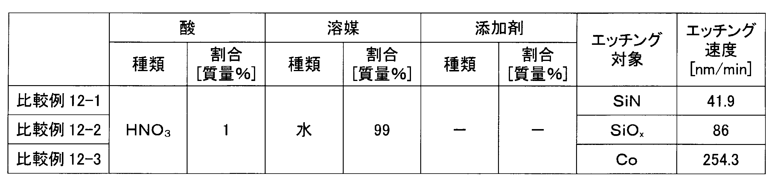
- a SiN, SiO x, and Co film was wet etched using 1% by mass of diluted nitric acid.
- the etching rate was calculated from the film thickness before and after wet etching of various films and the etching processing time.
- the selection ratio of Co and SiN or SiO x is 33 or more, and Fe and SiN Alternatively, the selection ratio to SiO x was 52 or more. Further, as shown in Examples 1-1 to 1-23 and Comparative Examples 1-1 to 1-5, the etching solution of the present invention selects a metal-containing film containing a predetermined metal element with respect to a silicon-based material. Etching was possible.
- the selection ratio of Co to SiN or SiO x is 25 or more.
- the selectivity ratio between Fe and SiN or SiO x was 46 or more, and the metal-containing film could be selectively etched with respect to the silicon-based material.
- the selection ratio of Co to SiN or SiO x is 28 or more.
- the selectivity ratio between Fe and SiN or SiO x was 48 or more, and the metal-containing film could be selectively etched with respect to the silicon-based material.
- the metal-containing film is selectively etched with respect to the silicon-based material regardless of whether the amount of HFAc is 5 mass% or 50 mass%. I was able to.
- Example 9-1 and Comparative Example 9-1 the metal-containing film could be selectively etched with respect to the silicon-based material even using an etching solution containing 1% by mass of moisture.
- the etching solution contained 5% by mass of water, so that particles were generated in the etching solution, and the particles remained in the object to be etched.
- the etching liquid from which particles remain cannot be used for etching a metal-containing film used in a semiconductor device.
Landscapes
- Chemical & Material Sciences (AREA)
- Chemical Kinetics & Catalysis (AREA)
- General Chemical & Material Sciences (AREA)
- Engineering & Computer Science (AREA)
- Materials Engineering (AREA)
- Mechanical Engineering (AREA)
- Metallurgy (AREA)
- Organic Chemistry (AREA)
- Weting (AREA)
- ing And Chemical Polishing (AREA)
- Manufacturing & Machinery (AREA)
Abstract
Description
本発明のウェットエッチング方法では、基板上の金属含有膜を、トリフルオロメチル基とカルボニル基が結合したβ-ジケトンを含むエッチング液を用いてエッチングする。
本発明に係るウェットエッチング方法により、従来の半導体製造プロセスで製造されるデバイスの金属含有膜をエッチング可能である。本発明に係るデバイスは、本発明に係るウェットエッチング方法によりエッチングした金属含有膜を用いることにより、安価に製造することができる。このようなデバイスとして、例えば、太陽電池、ハードディスクドライブ、ロジックIC、マイクロプロセッサ、ダイナミック・ランダム・アクセス・メモリ、相変化型メモリ、強誘電体メモリ、磁気抵抗メモリ、抵抗変化型メモリ、MEMS等を挙げることができる。


Claims (17)
- 基板上の金属含有膜を、エッチング液を用いてエッチングするウェットエッチング方法であって、
前記エッチング液が、トリフルオロメチル基とカルボニル基が結合したβ-ジケトンと、有機溶媒との溶液であり、
前記金属含有膜が、前記β-ジケトンと錯体を形成可能な金属元素を含むことを特徴とするウェットエッチング方法。 - 前記金属元素が、Ti,Zr,Hf,V,Nb,Ta,Cr,Mo,W,Mn,Re,Fe,Ru,Os,Co,Rh,Ir,Ni,Pd,Pt,Cu,Ag,Au,Zn,Cd,Al,Ga,In,Sn,Pb,及びAsからなる群より選ばれる少なくとも1種の金属元素であることを特徴とする請求項1に記載のウェットエッチング方法。
- 前記金属含有膜が、前記金属元素の単体の膜、前記金属元素を含む合金の膜、又は前記金属元素を含む化合物の膜のいずれかであることを特徴とする請求項1又は2に記載のウェットエッチング方法。
- 前記有機溶媒が、1級アルコール、2級アルコール、3級アルコール、ベンジルアルコール、エーテル、エステル、ケトン、アミン、アミド、グリコール、グリコールエーテル、及びハロゲン化アルカンからなる群より選ばれる少なくとも1種の有機溶媒であることを特徴とする請求項1~3のいずれか1項に記載のウェットエッチング方法。
- 前記有機溶媒が、イソプロピルアルコール、メタノール、エタノール、プロピレングリコールモノメチルエーテルアセテート(PGMEA)、メチルエチルケトン(MEK)、及びアセトンからなる群より選ばれる少なくとも1種の有機溶媒であることを特徴とする請求項4に記載のウェットエッチング方法。
- 前記エッチング液中に含まれる水の量が、1質量%以下であることを特徴とする請求項1~5のいずれか1項に記載のウェットエッチング方法。
- 前記エッチング液中の前記β-ジケトンの濃度が1~80体積%であることを特徴とする請求項1~6のいずれか1項に記載のウェットエッチング方法。
- 前記β-ジケトンが、ヘキサフルオロアセチルアセトン、トリフルオロアセチルアセトン、1,1,1,6,6,6-ヘキサフルオロ-2,4-ヘキサンジオン、4,4,4-トリフルオロ-1-(2-チエニル)-1,3-ブタンジオン、4,4,4-トリフルオロ-1-フェニル-1,3-ブタンジオン、1,1,1,5,5,5-ヘキサフルオロ-3-メチル-2,4-ペンタンジオン、1,1,1,3,5,5,5-ヘプタフルオロ-2,4-ペンタンジオン及び1,1,1-トリフルオロ-5,5-ジメチル-2,4-ヘキサンジオンからなる群より選ばれる少なくとも1種であることを特徴とする請求項1~7のいずれか1項に記載のウェットエッチング方法。
- 前記エッチング液が、さらに過酸化物の添加剤を含むことを特徴とする請求項1~8のいずれか1項に記載のウェットエッチング方法。
- 前記添加剤が、過酸化水素、過酢酸、過炭酸ナトリウム、過硫酸アンモニウム、過硫酸ナトリウム、過硫酸カリウム及びペルオキシ硫酸カリウムからなる群より選ばれる少なくとも1種であることを特徴とする請求項9に記載のウェットエッチング方法。
- 前記基板の材料が、シリコン系半導体材料又はケイ酸塩ガラス材料であることを特徴とする請求項1~10のいずれか1項に記載のウェットエッチング方法。
- イソプロピルアルコール、メタノール、エタノール、プロピレングリコールモノメチルエーテルアセテート(PGMEA)、メチルエチルケトン(MEK)、及びアセトンからなる群より選ばれる少なくとも1種の有機溶媒と、トリフルオロメチル基とカルボニル基が結合したβ-ジケトンと、を含むことを特徴とするエッチング液。
- 前記β-ジケトンが、ヘキサフルオロアセチルアセトン、トリフルオロアセチルアセトン、1,1,1,6,6,6-ヘキサフルオロ-2,4-ヘキサンジオン、4,4,4-トリフルオロ-1-(2-チエニル)-1,3-ブタンジオン、4,4,4-トリフルオロ-1-フェニル-1,3-ブタンジオン、1,1,1,5,5,5-ヘキサフルオロ-3-メチル-2,4-ペンタンジオン、1,1,1,3,5,5,5-ヘプタフルオロ-2,4-ペンタンジオン及び1,1,1-トリフルオロ-5,5-ジメチル-2,4-ヘキサンジオンからなる群より選ばれる少なくとも1種であることを特徴とする請求項12に記載のエッチング液。
- 前記エッチング液中の前記β-ジケトンの濃度が1~80質量%であることを特徴とする請求項12又は13に記載のエッチング液。
- 前記エッチング液が、実質的に前記有機溶媒と前記β-ジケトンとのみからなる請求項12~14のいずれか1項に記載のエッチング液。
- 前記エッチング液が、さらに過酸化物の添加剤を含み、
前記エッチング液が、実質的に前記有機溶媒と、前記β-ジケトンと、前記添加剤のみからなることを特徴とする請求項12~14のいずれか1項に記載のエッチング液。 - 基板上の金属含有膜に対して、請求項1に記載のウェットエッチング方法を用いて、ウェットエッチングする工程を含むことを特徴とするデバイスの製造方法。
Priority Applications (6)
| Application Number | Priority Date | Filing Date | Title |
|---|---|---|---|
| US15/573,302 US20180138053A1 (en) | 2015-07-23 | 2016-06-22 | Wet Etching Method and Etching Solution |
| CN201680027447.5A CN107533971B (zh) | 2015-07-23 | 2016-06-22 | 湿式蚀刻方法和蚀刻液 |
| KR1020217001825A KR20210010656A (ko) | 2015-07-23 | 2016-06-22 | 웨트 에칭 방법 및 에칭액 |
| KR1020227045292A KR102509446B1 (ko) | 2015-07-23 | 2016-06-22 | 웨트 에칭 방법 및 에칭액 |
| KR1020187002162A KR20180020273A (ko) | 2015-07-23 | 2016-06-22 | 웨트 에칭 방법 및 에칭액 |
| CN202110075293.XA CN112921320B (zh) | 2015-07-23 | 2016-06-22 | 湿式蚀刻方法和蚀刻液 |
Applications Claiming Priority (2)
| Application Number | Priority Date | Filing Date | Title |
|---|---|---|---|
| JP2015145487 | 2015-07-23 | ||
| JP2015-145487 | 2015-07-23 |
Publications (1)
| Publication Number | Publication Date |
|---|---|
| WO2017013988A1 true WO2017013988A1 (ja) | 2017-01-26 |
Family
ID=57833931
Family Applications (1)
| Application Number | Title | Priority Date | Filing Date |
|---|---|---|---|
| PCT/JP2016/068456 Ceased WO2017013988A1 (ja) | 2015-07-23 | 2016-06-22 | ウェットエッチング方法及びエッチング液 |
Country Status (6)
| Country | Link |
|---|---|
| US (1) | US20180138053A1 (ja) |
| JP (1) | JP6761166B2 (ja) |
| KR (3) | KR20180020273A (ja) |
| CN (2) | CN112921320B (ja) |
| TW (1) | TWI661089B (ja) |
| WO (1) | WO2017013988A1 (ja) |
Cited By (2)
| Publication number | Priority date | Publication date | Assignee | Title |
|---|---|---|---|---|
| CN113161259A (zh) * | 2020-01-23 | 2021-07-23 | 东京毅力科创株式会社 | 基板处理装置、基板处理方法和化学溶液 |
| JPWO2022149565A1 (ja) * | 2021-01-07 | 2022-07-14 |
Families Citing this family (17)
| Publication number | Priority date | Publication date | Assignee | Title |
|---|---|---|---|---|
| US12112959B2 (en) | 2018-09-04 | 2024-10-08 | Tokyo Electron Limited | Processing systems and platforms for roughness reduction of materials using illuminated etch solutions |
| CN113302730B (zh) * | 2018-12-14 | 2024-11-22 | 东京毅力科创株式会社 | 使用照射刻蚀溶液来降低材料粗糙度的加工系统和平台 |
| WO2020166677A1 (ja) | 2019-02-13 | 2020-08-20 | 株式会社トクヤマ | オニウム塩を含む半導体ウェハの処理液 |
| JP7303688B2 (ja) | 2019-07-31 | 2023-07-05 | 株式会社ディスコ | ウエットエッチング方法 |
| JP7303689B2 (ja) | 2019-07-31 | 2023-07-05 | 株式会社ディスコ | エッチング装置およびウェーハ支持具 |
| CN111180361A (zh) * | 2019-12-13 | 2020-05-19 | 贵州航天计量测试技术研究所 | 一种塑封器件湿法开封方法 |
| JP7489885B2 (ja) * | 2020-01-23 | 2024-05-24 | 東京エレクトロン株式会社 | 基板処理装置、基板処理方法及び薬液 |
| WO2022080288A1 (ja) * | 2020-10-16 | 2022-04-21 | セントラル硝子株式会社 | ウェットエッチング方法 |
| CN112259455B (zh) * | 2020-10-19 | 2024-01-26 | 扬州扬杰电子科技股份有限公司 | 一种改善带钝化层结构的Ag面产品金属残留的方法 |
| KR102659176B1 (ko) | 2020-12-28 | 2024-04-23 | 삼성디스플레이 주식회사 | 은 함유 박막의 식각 조성물, 이를 이용한 패턴 형성 방법 및 표시장치의 제조 방법 |
| KR102877343B1 (ko) | 2021-02-22 | 2025-10-27 | 삼성전자주식회사 | 식각용 조성물 및 이를 이용한 반도체 장치 제조 방법 |
| US12482702B2 (en) | 2022-09-12 | 2025-11-25 | Tokyo Electron Limited | Wet etch process and methods to form air gaps between metal interconnects |
| US12148624B2 (en) | 2022-09-12 | 2024-11-19 | Tokyo Electron Limited | Wet etch process and method to control fin height and channel area in a fin field effect transistor (FinFET) |
| US12100599B2 (en) | 2022-09-12 | 2024-09-24 | Tokyo Electron Limited | Wet etch process and method to provide uniform etching of material formed within features having different critical dimension (CD) |
| US12100598B2 (en) | 2022-09-12 | 2024-09-24 | Tokyo Electron Limited | Methods for planarizing a substrate using a combined wet etch and chemical mechanical polishing (CMP) process |
| US12148625B2 (en) | 2022-09-16 | 2024-11-19 | Tokyo Electron Limited | Methods to prevent surface charge induced cd-dependent etching of material formed within features on a patterned substrate |
| US12243749B2 (en) | 2022-09-26 | 2025-03-04 | Tokyo Electron Limited | Methods to provide uniform wet etching of material within high aspect ratio features provided on a patterned substrate |
Citations (4)
| Publication number | Priority date | Publication date | Assignee | Title |
|---|---|---|---|---|
| JPS5992916A (ja) * | 1982-11-19 | 1984-05-29 | Mitsubishi Metal Corp | 4a族金属の透明酸化物膜形成用組成物 |
| JPH09304947A (ja) * | 1996-05-17 | 1997-11-28 | Tokyo Ohka Kogyo Co Ltd | 金属酸化膜形成用塗布膜剥離液、剥離方法および基板の回収方法 |
| JP2014029939A (ja) * | 2012-07-31 | 2014-02-13 | Advanced Technology Materials Inc | 酸化ハフニウム用エッチング組成物 |
| WO2014197808A1 (en) * | 2013-06-06 | 2014-12-11 | Advanced Technology Materials, Inc. | Compositions and methods for selectively etching titanium nitride |
Family Cites Families (23)
| Publication number | Priority date | Publication date | Assignee | Title |
|---|---|---|---|---|
| JPH06326059A (ja) * | 1993-05-17 | 1994-11-25 | Fujitsu Ltd | 銅薄膜のエッチング方法 |
| US5782986A (en) * | 1996-01-11 | 1998-07-21 | Fsi International | Process for metals removal using beta-diketone or beta-ketoimine ligand forming compounds |
| JP4661005B2 (ja) * | 2000-09-05 | 2011-03-30 | 和光純薬工業株式会社 | Ti系膜用エッチング剤及びエッチング方法 |
| US7357138B2 (en) * | 2002-07-18 | 2008-04-15 | Air Products And Chemicals, Inc. | Method for etching high dielectric constant materials and for cleaning deposition chambers for high dielectric constant materials |
| EP1673802A1 (en) * | 2003-10-14 | 2006-06-28 | EKC Technology, INC. | REMOVAL OF POST ETCH RESIDUES AND COPPER CONTAMINATION FROM LOW-K DIELECTRICS USING SUPERCRITICAL CO sb 2 /sb WITH DIKETONE ADDITIVES |
| US20060054595A1 (en) | 2004-09-10 | 2006-03-16 | Honeywell International Inc. | Selective hafnium oxide etchant |
| EP1880410A2 (en) | 2005-05-13 | 2008-01-23 | Sachem, Inc. | Selective wet etching of oxides |
| TW200745313A (en) * | 2006-05-26 | 2007-12-16 | Wako Pure Chem Ind Ltd | Substrate etching liquid |
| SG177915A1 (en) * | 2006-12-21 | 2012-02-28 | Advanced Tech Materials | Liquid cleaner for the removal of post-etch residues |
| JP2012504871A (ja) * | 2008-10-02 | 2012-02-23 | アドバンスド テクノロジー マテリアルズ,インコーポレイテッド | 高度な金属負荷及びシリコン基板の表面パッシベーションのための界面活性剤/消泡剤混合物の使用 |
| US8349724B2 (en) * | 2008-12-31 | 2013-01-08 | Applied Materials, Inc. | Method for improving electromigration lifetime of copper interconnection by extended post anneal |
| US8128755B2 (en) * | 2010-03-03 | 2012-03-06 | L'air Liquide Societe Anonyme Pour L'etude Et L'exploitation Des Procedes Georges Claude | Cleaning solvent and cleaning method for metallic compound |
| TW201634701A (zh) * | 2010-04-15 | 2016-10-01 | 安堤格里斯公司 | 廢棄印刷電路板之回收利用方法 |
| EP2593964A4 (en) * | 2010-07-16 | 2017-12-06 | Entegris Inc. | Aqueous cleaner for the removal of post-etch residues |
| JP2012114287A (ja) | 2010-11-25 | 2012-06-14 | Tokyo Electron Ltd | パターン化金属膜及びその形成方法 |
| WO2012154498A2 (en) * | 2011-05-06 | 2012-11-15 | Advanced Technology Materials, Inc. | Removal of metal impurities from silicon surfaces for solar cell and semiconductor applications |
| JP5396514B2 (ja) | 2011-06-30 | 2014-01-22 | 富士フイルム株式会社 | エッチング方法及びこれに用いられるエッチング液、これを用いた半導体基板製品の製造方法 |
| JP5913869B2 (ja) * | 2011-08-31 | 2016-04-27 | 林純薬工業株式会社 | エッチング液組成物およびエッチング方法 |
| JP2013149852A (ja) | 2012-01-20 | 2013-08-01 | Toray Eng Co Ltd | 太陽電池の製造方法 |
| KR20140134283A (ko) * | 2012-03-12 | 2014-11-21 | 가부시끼가이샤 제이씨유 | 선택적 에칭방법 |
| US9460934B2 (en) * | 2013-03-15 | 2016-10-04 | Globalfoundries Inc. | Wet strip process for an antireflective coating layer |
| JP6142676B2 (ja) | 2013-05-31 | 2017-06-07 | セントラル硝子株式会社 | ドライエッチング方法、ドライエッチング装置、金属膜及びそれを備えたデバイス |
| US9570320B2 (en) * | 2014-10-09 | 2017-02-14 | Lam Research Corporation | Method to etch copper barrier film |
-
2016
- 2016-06-20 JP JP2016121414A patent/JP6761166B2/ja active Active
- 2016-06-22 KR KR1020187002162A patent/KR20180020273A/ko not_active Ceased
- 2016-06-22 WO PCT/JP2016/068456 patent/WO2017013988A1/ja not_active Ceased
- 2016-06-22 US US15/573,302 patent/US20180138053A1/en not_active Abandoned
- 2016-06-22 KR KR1020217001825A patent/KR20210010656A/ko not_active Ceased
- 2016-06-22 CN CN202110075293.XA patent/CN112921320B/zh active Active
- 2016-06-22 KR KR1020227045292A patent/KR102509446B1/ko active Active
- 2016-06-22 CN CN201680027447.5A patent/CN107533971B/zh active Active
- 2016-07-05 TW TW105121268A patent/TWI661089B/zh active
Patent Citations (4)
| Publication number | Priority date | Publication date | Assignee | Title |
|---|---|---|---|---|
| JPS5992916A (ja) * | 1982-11-19 | 1984-05-29 | Mitsubishi Metal Corp | 4a族金属の透明酸化物膜形成用組成物 |
| JPH09304947A (ja) * | 1996-05-17 | 1997-11-28 | Tokyo Ohka Kogyo Co Ltd | 金属酸化膜形成用塗布膜剥離液、剥離方法および基板の回収方法 |
| JP2014029939A (ja) * | 2012-07-31 | 2014-02-13 | Advanced Technology Materials Inc | 酸化ハフニウム用エッチング組成物 |
| WO2014197808A1 (en) * | 2013-06-06 | 2014-12-11 | Advanced Technology Materials, Inc. | Compositions and methods for selectively etching titanium nitride |
Cited By (3)
| Publication number | Priority date | Publication date | Assignee | Title |
|---|---|---|---|---|
| CN113161259A (zh) * | 2020-01-23 | 2021-07-23 | 东京毅力科创株式会社 | 基板处理装置、基板处理方法和化学溶液 |
| JPWO2022149565A1 (ja) * | 2021-01-07 | 2022-07-14 | ||
| WO2022149565A1 (ja) * | 2021-01-07 | 2022-07-14 | セントラル硝子株式会社 | ウェットエッチング溶液及びウェットエッチング方法 |
Also Published As
| Publication number | Publication date |
|---|---|
| KR20180020273A (ko) | 2018-02-27 |
| KR20210010656A (ko) | 2021-01-27 |
| US20180138053A1 (en) | 2018-05-17 |
| JP2017028257A (ja) | 2017-02-02 |
| CN107533971B (zh) | 2021-01-26 |
| TWI661089B (zh) | 2019-06-01 |
| CN112921320A (zh) | 2021-06-08 |
| CN107533971A (zh) | 2018-01-02 |
| KR20230006034A (ko) | 2023-01-10 |
| TW201708613A (zh) | 2017-03-01 |
| JP6761166B2 (ja) | 2020-09-23 |
| KR102509446B1 (ko) | 2023-03-14 |
| CN112921320B (zh) | 2023-04-28 |
Similar Documents
| Publication | Publication Date | Title |
|---|---|---|
| JP6761166B2 (ja) | ウェットエッチング方法及びエッチング液 | |
| CN107148664B (zh) | 用于清洗半导体元件的包含碱土金属的清洗液、和使用其的半导体元件的清洗方法 | |
| KR101282177B1 (ko) | 티탄계 금속, 텅스텐계 금속, 티탄-텅스텐계 금속 또는 그것들의 질화물의 에칭액 | |
| TWI612573B (zh) | 乾蝕刻方法、半導體元件之製造方法以及腔室清潔方法 | |
| JP6733476B2 (ja) | 半導体素子の洗浄用液体組成物、半導体素子の洗浄方法および半導体素子の製造方法 | |
| JP7504081B2 (ja) | エッチング組成物 | |
| TWI678601B (zh) | 可抑制含鎢材料之損壞的半導體元件之清洗液及利用該清洗液的半導體元件之清洗方法 | |
| KR102798242B1 (ko) | 에칭액, 피처리체의 처리 방법, 및 반도체 소자의 제조 방법 | |
| TWI856091B (zh) | 蝕刻組成物 | |
| WO2015095175A1 (en) | Ni:nige:ge selective etch formulations and method of using same | |
| JP2016127065A (ja) | エッチング液、これを用いたエッチング方法および半導体基板製品の製造方法 | |
| CN106952803A (zh) | 半导体元件的清洗用液体组合物及半导体元件的清洗方法、以及半导体元件的制造方法 | |
| JP2013004871A (ja) | 金属エッチング用組成物、および金属エッチング用組成物を用いた半導体装置の製造方法 | |
| WO2014178326A1 (ja) | エッチング液 | |
| TW202235683A (zh) | 濕式蝕刻溶液及濕式蝕刻方法 | |
| JP7791441B2 (ja) | ウェットエッチング方法 | |
| TW202132541A (zh) | 蝕刻液、蝕刻液之製造方法、被處理物之處理方法,及含有釕的配線之製造方法 | |
| JP2016157714A (ja) | エッチング液、エッチング方法および半導体基板製品の製造方法 | |
| JP6378271B2 (ja) | タングステン膜エッチング液組成物、これを用いた電子デバイスの製造方法および電子デバイス | |
| KR101985167B1 (ko) | 금속 식각액 조성물 및 이를 이용한 금속층의 식각 방법 | |
| JP2025522381A5 (ja) | ||
| JP2005064064A (ja) | エッチング剤及びエッチング方法 |
Legal Events
| Date | Code | Title | Description |
|---|---|---|---|
| 121 | Ep: the epo has been informed by wipo that ep was designated in this application |
Ref document number: 16827552 Country of ref document: EP Kind code of ref document: A1 |
|
| WWE | Wipo information: entry into national phase |
Ref document number: 15573302 Country of ref document: US |
|
| ENP | Entry into the national phase |
Ref document number: 20187002162 Country of ref document: KR Kind code of ref document: A |
|
| NENP | Non-entry into the national phase |
Ref country code: DE |
|
| 122 | Ep: pct application non-entry in european phase |
Ref document number: 16827552 Country of ref document: EP Kind code of ref document: A1 |