WO2016203705A1 - 半導体装置 - Google Patents
半導体装置 Download PDFInfo
- Publication number
- WO2016203705A1 WO2016203705A1 PCT/JP2016/002392 JP2016002392W WO2016203705A1 WO 2016203705 A1 WO2016203705 A1 WO 2016203705A1 JP 2016002392 W JP2016002392 W JP 2016002392W WO 2016203705 A1 WO2016203705 A1 WO 2016203705A1
- Authority
- WO
- WIPO (PCT)
- Prior art keywords
- heat sink
- bonding layer
- elements
- semiconductor device
- plastic strain
- Prior art date
- Legal status (The legal status is an assumption and is not a legal conclusion. Google has not performed a legal analysis and makes no representation as to the accuracy of the status listed.)
- Ceased
Links
Images



Classifications
-
- H—ELECTRICITY
- H10—SEMICONDUCTOR DEVICES; ELECTRIC SOLID-STATE DEVICES NOT OTHERWISE PROVIDED FOR
- H10W—GENERIC PACKAGES, INTERCONNECTIONS, CONNECTORS OR OTHER CONSTRUCTIONAL DETAILS OF DEVICES COVERED BY CLASS H10
- H10W90/00—Package configurations
-
- H—ELECTRICITY
- H10—SEMICONDUCTOR DEVICES; ELECTRIC SOLID-STATE DEVICES NOT OTHERWISE PROVIDED FOR
- H10W—GENERIC PACKAGES, INTERCONNECTIONS, CONNECTORS OR OTHER CONSTRUCTIONAL DETAILS OF DEVICES COVERED BY CLASS H10
- H10W70/00—Package substrates; Interposers; Redistribution layers [RDL]
- H10W70/20—Conductive package substrates serving as an interconnection, e.g. metal plates
-
- H—ELECTRICITY
- H10—SEMICONDUCTOR DEVICES; ELECTRIC SOLID-STATE DEVICES NOT OTHERWISE PROVIDED FOR
- H10W—GENERIC PACKAGES, INTERCONNECTIONS, CONNECTORS OR OTHER CONSTRUCTIONAL DETAILS OF DEVICES COVERED BY CLASS H10
- H10W72/00—Interconnections or connectors in packages
-
- H—ELECTRICITY
- H10—SEMICONDUCTOR DEVICES; ELECTRIC SOLID-STATE DEVICES NOT OTHERWISE PROVIDED FOR
- H10W—GENERIC PACKAGES, INTERCONNECTIONS, CONNECTORS OR OTHER CONSTRUCTIONAL DETAILS OF DEVICES COVERED BY CLASS H10
- H10W74/00—Encapsulations, e.g. protective coatings
- H10W74/40—Encapsulations, e.g. protective coatings characterised by their materials
-
- H—ELECTRICITY
- H10—SEMICONDUCTOR DEVICES; ELECTRIC SOLID-STATE DEVICES NOT OTHERWISE PROVIDED FOR
- H10W—GENERIC PACKAGES, INTERCONNECTIONS, CONNECTORS OR OTHER CONSTRUCTIONAL DETAILS OF DEVICES COVERED BY CLASS H10
- H10W76/00—Containers; Fillings or auxiliary members therefor; Seals
- H10W76/40—Fillings or auxiliary members in containers, e.g. centering rings
-
- H—ELECTRICITY
- H10—SEMICONDUCTOR DEVICES; ELECTRIC SOLID-STATE DEVICES NOT OTHERWISE PROVIDED FOR
- H10D—INORGANIC ELECTRIC SEMICONDUCTOR DEVICES
- H10D62/00—Semiconductor bodies, or regions thereof, of devices having potential barriers
- H10D62/10—Shapes, relative sizes or dispositions of the regions of the semiconductor bodies; Shapes of the semiconductor bodies
- H10D62/124—Shapes, relative sizes or dispositions of the regions of semiconductor bodies or of junctions between the regions
-
- H—ELECTRICITY
- H10—SEMICONDUCTOR DEVICES; ELECTRIC SOLID-STATE DEVICES NOT OTHERWISE PROVIDED FOR
- H10D—INORGANIC ELECTRIC SEMICONDUCTOR DEVICES
- H10D62/00—Semiconductor bodies, or regions thereof, of devices having potential barriers
- H10D62/80—Semiconductor bodies, or regions thereof, of devices having potential barriers characterised by the materials
- H10D62/83—Semiconductor bodies, or regions thereof, of devices having potential barriers characterised by the materials being Group IV materials, e.g. B-doped Si or undoped Ge
- H10D62/832—Semiconductor bodies, or regions thereof, of devices having potential barriers characterised by the materials being Group IV materials, e.g. B-doped Si or undoped Ge being Group IV materials comprising two or more elements, e.g. SiGe
- H10D62/8325—Silicon carbide
-
- H—ELECTRICITY
- H10—SEMICONDUCTOR DEVICES; ELECTRIC SOLID-STATE DEVICES NOT OTHERWISE PROVIDED FOR
- H10W—GENERIC PACKAGES, INTERCONNECTIONS, CONNECTORS OR OTHER CONSTRUCTIONAL DETAILS OF DEVICES COVERED BY CLASS H10
- H10W72/00—Interconnections or connectors in packages
- H10W72/071—Connecting or disconnecting
- H10W72/073—Connecting or disconnecting of die-attach connectors
- H10W72/07351—Connecting or disconnecting of die-attach connectors characterised by changes in properties of the die-attach connectors during connecting
-
- H—ELECTRICITY
- H10—SEMICONDUCTOR DEVICES; ELECTRIC SOLID-STATE DEVICES NOT OTHERWISE PROVIDED FOR
- H10W—GENERIC PACKAGES, INTERCONNECTIONS, CONNECTORS OR OTHER CONSTRUCTIONAL DETAILS OF DEVICES COVERED BY CLASS H10
- H10W72/00—Interconnections or connectors in packages
- H10W72/071—Connecting or disconnecting
- H10W72/073—Connecting or disconnecting of die-attach connectors
- H10W72/07351—Connecting or disconnecting of die-attach connectors characterised by changes in properties of the die-attach connectors during connecting
- H10W72/07355—Connecting or disconnecting of die-attach connectors characterised by changes in properties of the die-attach connectors during connecting changes in materials
-
- H—ELECTRICITY
- H10—SEMICONDUCTOR DEVICES; ELECTRIC SOLID-STATE DEVICES NOT OTHERWISE PROVIDED FOR
- H10W—GENERIC PACKAGES, INTERCONNECTIONS, CONNECTORS OR OTHER CONSTRUCTIONAL DETAILS OF DEVICES COVERED BY CLASS H10
- H10W72/00—Interconnections or connectors in packages
- H10W72/30—Die-attach connectors
-
- H—ELECTRICITY
- H10—SEMICONDUCTOR DEVICES; ELECTRIC SOLID-STATE DEVICES NOT OTHERWISE PROVIDED FOR
- H10W—GENERIC PACKAGES, INTERCONNECTIONS, CONNECTORS OR OTHER CONSTRUCTIONAL DETAILS OF DEVICES COVERED BY CLASS H10
- H10W72/00—Interconnections or connectors in packages
- H10W72/30—Die-attach connectors
- H10W72/351—Materials of die-attach connectors
-
- H—ELECTRICITY
- H10—SEMICONDUCTOR DEVICES; ELECTRIC SOLID-STATE DEVICES NOT OTHERWISE PROVIDED FOR
- H10W—GENERIC PACKAGES, INTERCONNECTIONS, CONNECTORS OR OTHER CONSTRUCTIONAL DETAILS OF DEVICES COVERED BY CLASS H10
- H10W72/00—Interconnections or connectors in packages
- H10W72/30—Die-attach connectors
- H10W72/381—Auxiliary members
-
- H—ELECTRICITY
- H10—SEMICONDUCTOR DEVICES; ELECTRIC SOLID-STATE DEVICES NOT OTHERWISE PROVIDED FOR
- H10W—GENERIC PACKAGES, INTERCONNECTIONS, CONNECTORS OR OTHER CONSTRUCTIONAL DETAILS OF DEVICES COVERED BY CLASS H10
- H10W90/00—Package configurations
- H10W90/701—Package configurations characterised by the relative positions of pads or connectors relative to package parts
- H10W90/731—Package configurations characterised by the relative positions of pads or connectors relative to package parts of die-attach connectors
- H10W90/736—Package configurations characterised by the relative positions of pads or connectors relative to package parts of die-attach connectors between a chip and a stacked lead frame, conducting package substrate or heat sink
Definitions
- This disclosure relates to a semiconductor device in which a plurality of elements are driven in parallel.
- SiC silicon carbide
- a switching element containing SiC as a main component has a lower on-resistance than a device containing silicon as a main component, and can reduce power loss.
- it can operate under high-temperature conditions as compared with silicon, and downsizing of the cooling mechanism is expected.
- an insulated gate bipolar transistor (IGBT) and a free-wheeling diode (FWD) are connected in parallel to form an inverter.
- IGBT insulated gate bipolar transistor
- FWD free-wheeling diode
- recovery loss and switching loss are reduced by adopting SiC as a constituent material of the FWD, thereby reducing the amount of heat generated in the FWD. Therefore, the allowable operating temperature of the FWD can be expanded together with the feature of SiC that it can be used in a high temperature range, and the size can be reduced by suppressing the capacity of the cooling mechanism.
- some semiconductor temperature sensors such as a PN junction temperature sensor are disposed on an element to detect temperature, and a means for protecting the element against a temperature rise above a specified level is taken.
- wide band gap semiconductors are generally expensive, and there is a risk that adding a semiconductor temperature sensor to an element that employs a wide band gap semiconductor as a constituent material may lead to an increase in cost.
- the present disclosure relates to a semiconductor device including a semiconductor element composed of components different from each other, and capable of performing thermal protection of the element without providing a temperature detection means on the side of the semiconductor element composed of one component
- the purpose is to provide.
- a semiconductor device includes at least one first element, at least one second element, a heat sink, a first bonding layer, a second bonding layer, and a mold resin.
- the first element is formed with the first component as a main component, and electrodes are provided on one surface and the opposite back surface.
- the second element is formed with a second component different from the first component as a main component, and an electrode is provided on one surface and the opposite back surface.
- the first element and the second element are placed on the heat sink.
- the first bonding layer electrically bonds the electrode on the back surface side of the first element and the heat sink.
- the second bonding layer electrically bonds the electrode on the back surface side of the second element and the heat sink.
- the mold resin covers and protects the first element, the second element, and the heat sink while exposing a part of the surface of the heat sink.
- the physique of the first element and the second element is set so that the equivalent plastic strain increment of the first bonding layer is larger than that of the second bonding layer.
- the strain amount of the first bonding layer is larger than that of the second bonding layer, and cracks are likely to occur in the first bonding layer, so that the amount of increase in the thermal resistance of the first bonding layer is also increased. That is, the first bonding layer can reach a specified life before the second bonding layer. That is, since the designer can determine the bonding layer that reaches the end of its life in advance, the temperature detecting means is formed only on the first element side to which the first bonding layer is connected, and the element heat is detected based on the detected temperature. If the protective protection is performed, it is possible to prevent the second element from failing first.
- FIG. 1 is a circuit diagram showing a circuit configuration of a semiconductor device and its peripheral circuits in a first embodiment; It is a top view showing a schematic configuration of a semiconductor device, FIG. 3 is a sectional view taken along line III-III in FIG. It is a perspective view showing a detailed structure of a part of the semiconductor device, It is a figure showing the change of the equivalent plastic strain increment with respect to the length of one side of the chip, 10 is a top view illustrating a schematic configuration of a semiconductor device according to Modification 1.
- FIG. 1 is a circuit diagram showing a circuit configuration of a semiconductor device and its peripheral circuits in a first embodiment; It is a top view showing a schematic configuration of a semiconductor device, FIG. 3 is a sectional view taken along line III-III in FIG. It is a perspective view showing a detailed structure of a part of the semiconductor device, It is a figure showing the change of the equivalent plastic strain increment with respect to the length of one side of the chip, 10 is a top view illustrating a
- the semiconductor device is used for a switch circuit that obtains an output current by connecting two switching elements of a MOSFET and an IGBT in parallel, for example.
- the IGBT has a characteristic of generating a tail current when it is turned off. This tail current causes a large switching loss at turn-off.
- the power consumption caused by the tail current is suppressed by delaying the MOSFET off timing from the IGBT.
- the semiconductor device 100 in the present embodiment is a switch circuit, and two semiconductor devices 100 are connected in series between a power supply VCC and a ground GND to constitute an upper arm and a lower arm.
- a load 200 is connected between the upper arm and the lower arm, and the direction of the current flowing through the load 200 is switched by alternately turning on and off the semiconductor device 100 that bears the upper arm and the semiconductor device 100 that bears the lower arm.
- the two semiconductor devices 100 constitute an inverter.
- the semiconductor device 100 includes an IGBT 10 as a first element and a MOSFET 20 as a second element, and these are connected in parallel to the power supply VCC.
- a driver 300 for supplying a gate voltage to each of the switching elements 10 and 20 is connected to the gate electrodes of the IGBT 10 and the MOSFET 20.
- the driver 300 is connected to a control device (not shown) for controlling the on / off timing of the IGBT 10 and the MOSFET 20 and the voltage value of the gate voltage.
- the driver 300 controls the IGBT 10 and the MOSFET 20 based on an instruction signal input from the control device.
- the semiconductor device 100 includes the chip-like IGBT 10 and the MOSFET 20 as switching elements made of a semiconductor as described above.
- the first heat sink 30 and the second heat sink 40 each having a flat plate shape are provided for radiating heat generated by the switching elements 10 and 20.
- the IGBT 10 and the MOSFET 20 are arranged so as to be sandwiched between the first heat sink 30 and the second heat sink 40.
- the semiconductor device 100 includes a first spacer 70 and a second spacer 80 for adjusting a facing distance between the first heat sink 30 and the second heat sink 40. And it has mold resin 90 which protects these switching elements 10 and 20, heat sinks 30 and 40, and spacers 70 and 80.
- the IGBT 10 in the present embodiment has an emitter electrode formed on one surface thereof, and a collector electrode formed on the back surface opposite to the one surface. As shown in FIG. 3, the IGBT 10 is placed via the first bonding layer 50 so that the collector electrode is electrically connected to the first heat sink 30.
- the MOSFET 20 has a source electrode formed on one surface and a drain electrode formed on the back surface opposite to the one surface. As shown in FIG. 3, the MOSFET 20 is placed via the second bonding layer 60 so that the drain electrode is electrically connected to the first heat sink 30.
- the first heat sink 30 and the second heat sink 40 are flat members for radiating the heat generated by the IGBT 10 and the MOSFET 20 to the outside, and the first heat sink 30 and the second heat sink 40 are arranged to face each other. Yes.
- the IGBT 10 and the MOSFET 20 are mounted by being sandwiched between the heat sinks 30 and 40, and the second heat sink 40 is opposed to the emitter electrode of the IGBT 10 and the source electrode of the MOSFET 20.
- the first heat sink 30 has a protruding portion T1 protruding from a part of one side of the flat plate shape, and the protruding portion T1 is connected to the power supply VCC.
- the second heat sink 40 has a protruding portion T2 protruding from a part of one side of the flat plate shape, and the protruding portion T2 is connected to the load 200 and the lower arm.
- the second heat sink 40 and the emitter electrode of the IGBT 10 are connected via a first spacer 70. Further, the second heat sink 40 and the source electrode of the MOSFET 20 are connected via a second spacer 80.
- the spacers 70 and 80 adjust the facing distance between the heat sinks 30 and 40 so that the first heat sink 30 and the second heat sink 40 are parallel to each other, and electrically connect the IGBT 10 and the MOSFET 20 and the second heat sink 40 to each other. It is a member to connect.
- the first spacer 70 is connected to the emitter electrode of the IGBT 10 through the third bonding layer 71. Further, the first spacer 70 is connected to the second heat sink 40 via the fourth bonding layer 72. On the other hand, the second spacer 80 is connected to the source electrode of the MOSFET 20 through the fifth bonding layer 81. The second spacer 80 is connected to the second heat sink 40 via the sixth bonding layer 82.
- Mold resin 90 includes IGBT 10, MOSFET 20, first spacer 70, second spacer 80, first bonding layer 50, second bonding layer 60, third bonding layer 71, fourth bonding layer 72, fifth bonding layer 81, and The sixth bonding layer 82 is molded so as to be protected.
- the first heat sink 30 has a surface 30a on which the IGBT 10 and the MOSFET 20 are not mounted exposed to the outside, and the protrusion T1 protrudes to the outside as shown in FIG. It is insert molded.
- the second heat sink 40 is insert-molded so that the surface 40a to which the first spacer 70 and the second spacer 80 are not connected is exposed to the outside, and the protruding portion T2 protrudes to the outside.
- the driver 300 is also disposed so as to be included in the mold resin 90, and the gate electrodes of the IGBT 10 and the MOSFET 20 and the driver 300 are bonded to the bonding wires W1 and W2, respectively. Connected through.
- the driver 300 is not necessarily insert-molded in the mold resin 90 together with the semiconductor device 100, and may be disposed outside the mold resin 90.
- the IGBT 10 is formed with silicon as a first component as a main component.
- the MOSFET 20 is formed with silicon carbide as the second component as a main component.
- the first heat sink 30, the second heat sink 40, the first spacer 70, and the second spacer 80 are formed with copper as a main component.
- the first bonding layer 50, the second bonding layer 60, the third bonding layer 71, the fourth bonding layer 72, the fifth bonding layer 81, and the sixth bonding layer 82 are generally known solders. Note that the third bonding layer 71, the fourth bonding layer 72, the fifth bonding layer 81, and the sixth bonding layer 82 in this embodiment are thinner than the first bonding layer 50 and the second bonding layer 60, respectively. It is formed as follows.
- FIG. 4 elements other than the IGBT 10, the MOSFET 20, the first bonding layer 50, the second bonding layer 60, and the first heat sink 30 are not shown.
- the IGBT 10 forms a square when the flat surface of the first heat sink 30 is viewed in plan.
- one side on which the emitter electrode is formed or the back side on which the collector electrode is formed forms a square.
- the length of one side of the square is a1, as shown in FIG.
- the thickness of the IGBT 10 chip is b1.
- an equivalent plastic strain increment ⁇ 1 defined by ⁇ 1 (0.004b1 + 0.0003) a1 2 +0.26 is generated in the first bonding layer 50 containing solder as a main component.
- the definition equation of the equivalent plastic strain increment ⁇ 1 is an equation obtained by function fitting the equivalent plastic strain increment calculated by computer simulation using the length a1 and the thickness b1 as variables. In the computer simulation, physical quantities (for example, Young's modulus, Poisson's ratio, linear expansion coefficient) unique to the silicon constituting the IGBT 10 and the solder constituting the first bonding layer 50 are used.
- the MOSFET 20 has a square shape when the flat surface of the first heat sink 30 is viewed in plan.
- the one surface on which the source electrode is formed or the back surface on which the drain electrode is formed forms a square.
- the length of one side of this square is a2, as shown in FIG.
- the thickness of the chip of the MOSFET 20 is b2.
- the definition formula of the equivalent plastic strain increment ⁇ 2 is an equation obtained by function fitting the equivalent plastic strain increment calculated by computer simulation using the length a2 and the thickness b2 as variables.
- the amount of strain in the first bonding layer 50 is larger than that in the second bonding layer 60, so that the amount of increase in the thermal resistance of the first bonding layer 50 is increased in the second bonding layer 60. Larger than the amount. That is, the first bonding layer 50 can reach a specified life before the second bonding layer 60. That is, since the designer can intentionally control the bonding layer that reaches the end of its life in advance to be the first bonding layer 50, the temperature detecting means is provided only on the IGBT 10 side as the first element to which the first bonding layer 50 is connected. When the device is formed and the element is thermally protected based on the detected temperature, it is possible to prevent the MOSFET 20 as the second element from failing first.
- the chip size of the element mainly composed of silicon carbide can be reduced.
- Silicon carbide is generally more expensive than silicon. Therefore, by adopting this semiconductor device 100, it is possible to suppress an increase in the chip size of an element mainly composed of silicon carbide, and it is possible to suppress the cost for manufacturing the semiconductor device 100.
- a semiconductor device 110 having four IGBTs (IGBT11 to IGBT14) and four MOSFETs (MOSFET21 to MOSFET24) will be described.
- the IGBTs 11 to 14 and the MOSFETs 21 to 24 are mounted on the first heat sink 30 via corresponding bonding layers.
- the 2nd heat sink 40 is connected to the emitter electrode or source electrode of each element through the corresponding spacer. That is, as in the first embodiment, the first heat sink 30 and the second heat sink 40 are arranged to face each other.
- the driver 300 is not shown, but the driver 300 supplies gate voltages to the gate electrodes of the IGBTs 11 to 14 and the MOSFETs 21 to 24, respectively.
- the equivalent plastic strain increments that give stress to the bonding layers to which the IGBTs 11 to 14 correspond correspond to ⁇ 11 to ⁇ 14, respectively. Further, the equivalent plastic strain increments that give stress to the corresponding bonding layers by the MOSFETs 21 to 24 are denoted by ⁇ 21 to ⁇ 24, respectively.
- the physique of each element 11 to 14 and 21 to 24 in this embodiment is that the maximum value of the equivalent plastic strain increment of ⁇ 11 to ⁇ 14 is ⁇ 1max, and the maximum value of the equivalent plastic strain increment of ⁇ 21 to ⁇ 24 is ⁇ 2max. Then, each is set so as to satisfy the relationship of ⁇ 1max> ⁇ 2max.
- the thermal resistance of the junction layer corresponding to any one of the IGBT11 to IGBT14 exceeds the threshold value used for the failure determination prior to the MOSFET21 to MOSFET24. Therefore, since it is not necessary to provide a temperature detecting means on the MOSFET side, the chip size of the element mainly composed of silicon carbide can be reduced.
- the example in which silicon is employed as the constituent material of the first element and silicon carbide is employed as the constituent material of the second element has been described, but these constituent materials are not limited.
- the second element is silicon
- an effect that it is not necessary to provide temperature detecting means on the second element side can be exhibited.
- the physique of the whole semiconductor device can be reduced to the extent that the above means is not formed.
- gallium nitride and gallium oxide can be used in addition to silicon carbide.
- the so-called double-sided heat dissipation type semiconductor device in which the IGBTs 10 to 14 and the MOSFETs 20 to 24 are sandwiched between the two heat sinks 30 and 40 has been described.
- the present disclosure can be applied. That is, compared to the first embodiment, the second heat sink 40, the first spacer 70, the second spacer 80, the third bonding layer 71, the fourth bonding layer 72, the fifth bonding layer 81, and the sixth bonding layer 82. Even if it is a semiconductor device which does not have, the physique of IGBT10 and MOSFET20 should just be set so that the equivalent plastic strain increment of the 1st joining layer 50 may become larger than the 2nd joining layer 60.
Landscapes
- Cooling Or The Like Of Semiconductors Or Solid State Devices (AREA)
Abstract
半導体装置は、第1成分を主成分として形成された第1素子(10~14)と、第2成分を主成分として形成された第2素子(20~24)と、第1素子および第2素子が載置されるヒートシンク(30)と、第1素子とヒートシンクとを電気的に接合する第1接合層(50)と、第2素子とヒートシンクとを電気的に接合する第2接合層(60)と、第1素子、第2素子、およびヒートシンクを被覆して保護するモールド樹脂(90)を備える。第1素子および第2素子の体格は、第2接合層よりも第1接合層の相当塑性ひずみ増分が大きくなるように設定される。これにより、互いに異なる成分から構成される半導体素子を備える半導体装置において、一方の成分から構成される半導体素子側に温度検出手段を設けることなく、素子の熱的保護を行うことができる。
Description
本出願は、2015年6月18日に出願された日本出願番号2015-122981号に基づくもので、ここにその記載内容を援用する。
本開示は、複数の素子が並列で駆動される半導体装置に関するものである。
近年、複数の素子が並列で駆動される半導体装置において、一部の素子の構成材料にワイドバンドギャップ半導体と称される半導体の一種であるシリコンカーバイド(SiC)が採用されつつある。例えば、SiCを主成分とするスイッチング素子は、シリコンを主成分とするものに比較してオン抵抗が小さく電力損失を低減することができる。また、シリコンと比較して高温条件下で動作することができ、冷却機構の小型化が期待されている。
特許文献1記載のパワー半導体モジュールは、絶縁ゲートバイポーラトランジスタ(IGBT)と還流ダイオード(FWD)とが並列に接続され、インバータが構成されている。このパワー半導体モジュールでは、FWDの構成材料にSiCを採用することによってリカバリ損失およびスイッチング損失を低減してFWDにおける発熱量を低減させている。したがって、高温域での使用が可能であるというSiCの特徴と合わせて、FWDの許容動作温度を拡大でき、冷却機構の能力を抑制することによる小型化ができるとしている。
ところで、温度に対する素子の保護の観点から、素子を他の部材と電気的に接続する部材の、熱抵抗悪化を察知することが重要になる。従来、素子上にPN接合温度センサ等の半導体温度センサを配置して温度の検出を行うものがあり、規定以上の温度上昇に対して素子を保護する手段がとられる。
しかしながら、ワイドバンドギャップ半導体は一般に高価であり、ワイドバンドギャップ半導体を構成材料として採用した素子に対して半導体温度センサを併設することはコストアップに繋がる虞があった。
本開示は、互いに異なる成分から構成される半導体素子を備える半導体装置において、一方の成分から構成される半導体素子側に温度検出手段を設けることなく、素子の熱的保護を行うことのできる半導体装置を提供することを目的とする。
本開示の一態様によれば、半導体装置は、少なくとも一つの第1素子と、少なくとも一つの第2素子と、ヒートシンクと、第1接合層と、第2接合層と、モールド樹脂と、を備える。第1素子は、第1成分を主成分として形成され、一面とその反対の裏面に電極が設けられている。第2素子は、第1成分とは異なる第2成分を主成分として形成され、一面とその反対の裏面に電極が設けられている。ヒートシンクには、第1素子および第2素子が載置される。第一接合層は、第1素子の裏面側の電極とヒートシンクとを電気的に接合する。第2接合層は、第2素子の裏面側の電極とヒートシンクとを電気的に接合する。モールド樹脂は、ヒートシンクの表面の一部を露出しつつ、第1素子、第2素子、およびヒートシンクを被覆して保護する。第1素子および第2素子の体格は、第2接合層よりも第1接合層の相当塑性ひずみ増分が大きくなるように設定される。
これによれば、第2接合層よりも第1接合層の歪み量が大きくなり、第1接合層にクラックが発生しやすくなるため、第1接合層の熱抵抗の増加量も大きくなる。すなわち、第1接合層が第2接合層に先行して、規定される寿命を迎えるようにできる。つまり、設計者は先行して寿命を迎える接合層を決定できるので、第1接合層が接続される第1素子側にのみ温度検出手段を形成して、検出された温度に基づいて素子の熱的保護を行えば、第2素子が先に故障することを防止することができる。
本開示についての上記目的およびその他の目的、特徴や利点は、添付の図面を参照しながら下記の詳細な記述により、より明確になる。図面において、
第1実施形態における半導体装置およびその周辺回路の回路構成を示す回路図であり、
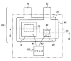
半導体装置の概略構成を示す上面図であり、
図2におけるIII-III線に沿う断面図であり、
半導体装置の一部について詳細構造を示す斜視図であり、
チップ一辺の長さに対する相当塑性ひずみ増分の変化をしめす図であり、
変形例1における半導体装置の概略構成を示す上面図である。
以下、本開示の実施の形態を図面に基づいて説明する。なお、以下の各図相互において、互いに同一もしくは均等である部分に、同一符号を付与する。
(第1実施形態)
最初に、図1~図3を参照して、本実施形態に係る半導体装置の概略構成について説明する。
最初に、図1~図3を参照して、本実施形態に係る半導体装置の概略構成について説明する。
本実施形態における半導体装置は、例えば、MOSFETとIGBTの2つのスイッチング素子を並列に接続して出力電流を得るスイッチ回路に供される。IGBTはそのターンオフ時にテール電流を発生する特性を有する。このテール電流は、ターンオフ時のスイッチング損失を大きくする原因となっている。これに対して、MOSFETとIGBTとが並列に接続された半導体装置にあっては、MOSFETのオフタイミングをIGBTよりも遅らせることにより、テール電流に起因する消費電力を抑制している。
まず、図1を参照して、本実施形態における半導体装置100および周辺回路の回路構成を説明する。図1に示すように、本実施形態における半導体装置100はスイッチ回路であり、電源VCCとグランドGNDの間において2つの半導体装置100が直列に接続されて上アームと下アームを構成している。上アームと下アームとの間には負荷200が接続され、上アームを担う半導体装置100と下アームを担う半導体装置100とが交互にオンオフすることによって負荷200に流れる電流の向きを切り替えている。すなわち、2つの半導体装置100はインバータを構成している。
上アームおよび下アームを構成する半導体装置100は互いに等価であるので、以降、上アームを構成する半導体装置100について説明する。
半導体装置100は、第1素子たるIGBT10と第2素子たるMOSFET20とを有し、これらが電源VCCに対して並列に接続されている。IGBT10およびMOSFET20のゲート電極には、それぞれのスイッチング素子10,20にゲート電圧を供給するためのドライバ300が接続されている。なお、ドライバ300には、IGBT10およびMOSFET20のオンオフのタイミングや、ゲート電圧の電圧値を制御するための図示しない制御装置が接続されている。ドライバ300は制御装置から入力される指示信号に基づいてIGBT10およびMOSFET20を制御している。
続いて、図2および図3を参照して、半導体装置100の実装構造について説明する。図2および図3に示すように、この半導体装置100は、上記したように、半導体より成るスイッチング素子として、チップ状のIGBT10とMOSFET20とを有している。また、スイッチング素子10,20が発生する熱の放熱のために、平板状の第1ヒートシンク30および第2ヒートシンク40を有している。IGBT10およびMOSFET20は第1ヒートシンク30と第2ヒートシンク40とに挟まれるように配置されている。さらに、この半導体装置100は、第1ヒートシンク30および第2ヒートシンク40との対向距離を調整するための第1スペーサ70および第2スペーサ80を有している。そして、これらスイッチング素子10,20、ヒートシンク30,40、スペーサ70,80を保護するモールド樹脂90を有している。
本実施形態におけるIGBT10はその一面にエミッタ電極が形成され、一面と反対の裏面にコレクタ電極が形成されている。IGBT10は、図3に示すように、コレクタ電極が第1ヒートシンク30に電気的に接続されるよう、第1接合層50を介して載置されている。一方、MOSFET20はその一面にソース電極が形成され、一面と反対の裏面にドレイン電極が形成されている。MOSFET20は、図3に示すように、ドレイン電極が第1ヒートシンク30に電気的に接続されるよう、第2接合層60を介して載置されている。
第1ヒートシンク30および第2ヒートシンク40は、IGBT10およびMOSFET20が発生する熱を外部へ放熱するための平板状の部材であり、第1ヒートシンク30と第2ヒートシンク40とは互いに対向して配置されている。上記したように、IGBT10およびMOSFET20はヒートシンク30,40に挟まれて実装されており、第2ヒートシンク40は、IGBT10のエミッタ電極、および、MOSFET20のソース電極と対向している。
第1ヒートシンク30は、図2に示すように、平板状の一辺の一部から突出した突出部T1を有しており、この突出部T1が電源VCCに接続されている。また、第2ヒートシンク40は、平板状の一辺の一部から突出した突出部T2を有しており、この突出部T2が負荷200および下アームに接続されている。
第2ヒートシンク40とIGBT10のエミッタ電極は第1スペーサ70を介して接続されている。また、第2ヒートシンク40とMOSFET20のソース電極は第2スペーサ80を介して接続されている。スペーサ70,80は、第1ヒートシンク30と第2ヒートシンク40とが互いに平行になるように、両ヒートシンク30,40の対向距離を調整するとともに、IGBT10およびMOSFET20と、第2ヒートシンク40と、を電気的に接続する部材である。
第1スペーサ70は、第3接合層71を介してIGBT10のエミッタ電極に接続されている。また、第1スペーサ70は、第4接合層72を介して第2ヒートシンク40に接続されている。一方、第2スペーサ80は、第5接合層81を介してMOSFET20のソース電極に接続されている。また、第2スペーサ80は、第6接合層82を介して第2ヒートシンク40に接続されている。
モールド樹脂90は、IGBT10、MOSFET20、第1スペーサ70、第2スペーサ80、第1接合層50、第2接合層60、第3接合層71、第4接合層72、第5接合層81、および、第6接合層82を内包して保護するように成型されている。また、図3に示すように、第1ヒートシンク30はIGBT10およびMOSFET20が実装されていない表面30aが外部に露出するようされ、且つ、図2に示すように、突出部T1が外部に突出するようにインサート成型されている。さらに、第2ヒートシンク40は第1スペーサ70および第2スペーサ80が接続されていない表面40aが外部に露出するようされ、且つ、突出部T2が外部に突出するようにインサート成型されている。
なお、本実施形態では、図2に示すように、ドライバ300もモールド樹脂90に内包されるように配置されており、IGBT10およびMOSFET20のゲート電極と、ドライバ300とは、それぞれボンディングワイヤW1およびW2を介して接続されている。ドライバ300は必ずしも半導体装置100とともにモールド樹脂90内にインサート成型される必要はなく、モールド樹脂90の外部に配置するようにしても良い。
本実施形態におけるIGBT10は第1成分たるシリコンを主成分として形成されている。また、MOSFET20は第2成分たるシリコンカーバイドを主成分として形成されている。また、第1ヒートシンク30、第2ヒートシンク40、第1スペーサ70および第2スペーサ80は銅を主成分として形成されている。さらに、第1接合層50、第2接合層60、第3接合層71、第4接合層72、第5接合層81、および、第6接合層82は一般的に知られたはんだである。なお、本実施形態における第3接合層71、第4接合層72、第5接合層81、および、第6接合層82は、それぞれ、第1接合層50および第2接合層60よりも薄くなるように形成されている。
続いて、図4および図5を参照して、IGBT10とMOSFET20の形状について詳しく説明する。なお、図4では、IGBT10、MOSFET20、第1接合層50、第2接合層60および第1ヒートシンク30を除く要素は図示を省略している。
IGBT10は、第1ヒートシンク30の平板たる面を平面視した場合に、正方形を成している。換言すれば、エミッタ電極が形成された一面あるいはコレクタ電極が形成された裏面が正方形を成している。この正方形の一辺の長さを、図4に示すように、a1とする。また、IGBT10のチップの厚さをb1とする。
このとき、はんだを主成分とする第1接合層50には、Δε1=(0.004b1+0.0003)a12+0.26により定義される相当塑性ひずみ増分Δε1が生じる。なお、相当塑性ひずみ増分Δε1の定義式は、長さa1と厚さb1とを変数としてコンピュータシミュレーションにより算出された相当塑性ひずみ増分を関数フィッティングして得られた式である。コンピュータシミュレーションには、IGBT10を構成するシリコンや、第1接合層50を構成するはんだに固有の物理量(例えばヤング率、ポアソン比、線膨張係数)が利用されている。
MOSFET20は、第1ヒートシンク30の平板たる面を平面視した場合に、正方形を成している。換言すれば、ソース電極が形成された一面あるいはドレイン電極が形成された裏面が正方形を成している。この正方形の一辺の長さを、図4に示すように、a2とする。また、MOSFET20のチップの厚さをb2とする。
このとき、第2接合層60には、Δε2=(0.0075b2+0.0003)a22+0.03により定義される相当塑性ひずみ増分Δε2が生じる。なお、相当塑性ひずみ増分Δε2の定義式は、長さa2と厚さb2とを変数としてコンピュータシミュレーションにより算出された相当塑性ひずみ増分を関数フィッティングして得られた式である。
そして、IGBT10およびMOSFET20の体格、すなわち、IGBT10の正方形の一辺の長さa1、厚さb1、および、MOSFET20の正方形の一辺の長さa2、厚さb2、がΔε1>Δε2の関係を満たすように、それぞれ設定されている。具体的には、図5に示すように、b1=b2とした上で、IGBT10のチップ一辺の長さa1をD1に設定し、MOSFET20のチップ一辺の長さa2をD2に設定することにより、Δε1>Δε2を実現する。
次に、本実施形態における半導体装置100を採用することによる作用効果について説明する。
本実施形態における半導体装置100を採用すると、第2接合層60よりも第1接合層50の歪み量が大きくなるため、第1接合層50の熱抵抗の増加量は第2接合層60における増加量よりも大きくなる。すなわち、第1接合層50が第2接合層60に先行して、規定される寿命を迎えるようにできる。つまり、設計者は先行して寿命を迎える接合層が第1接合層50となるように意図的に制御できるので、第1接合層50が接続される第1素子たるIGBT10側にのみ温度検出手段を形成して、検出された温度に基づいて素子の熱的保護を行えば、第2素子たるMOSFET20が先に故障することを防止することができる。
これによれば、シリコンカーバイドにより形成されたMOSFET20側に温度検出用の手段を設ける必要がないため、シリコンカーバイドを主成分とする素子のチップサイズを小さくすることができる。シリコンカーバイドは、一般にシリコンよりも高価である。よって、この半導体装置100を採用することにより、シリコンカーバイドを主成分とする素子のチップサイズの増大化を抑制でき、半導体装置100の製造にかかるコストを抑制することができる。
(変形例1)
第1実施形態では、第1素子たるIGBT10と、第2素子たるMOSFET20とを1つずつ有する半導体装置について説明したが、それぞれ複数の素子が一対の第1および第2ヒートシンク30,40の間に存在する形態であっても良い。
第1実施形態では、第1素子たるIGBT10と、第2素子たるMOSFET20とを1つずつ有する半導体装置について説明したが、それぞれ複数の素子が一対の第1および第2ヒートシンク30,40の間に存在する形態であっても良い。
例えば、図6に示すように、IGBTを4個(IGBT11~IGBT14)、MOSFETを4個(MOSFET21~MOSFET24)有する半導体装置110について説明する。この半導体装置110は、第1ヒートシンク30上に、IGBT11~14およびMOSFET21~24が、対応する接合層を介して載置されている。そして、それぞれの素子のエミッタ電極あるいはソース電極に、対応するスペーサを介して第2ヒートシンク40が接続されている。つまり、第1実施形態と同様に、第1ヒートシンク30と第2ヒートシンク40とは互いに対向して配置されている。なお、図6においては、ドライバ300の図示を省略しているが、ドライバ300は、IGBT11~14およびMOSFET21~24のゲート電極にそれぞれゲート電圧を供給している。
ここで、IGBT11~IGBT14が対応する接合層に対して応力を与える相当塑性ひずみ増分を、それぞれΔε11~Δε14とする。また、MOSFET21~MOSFET24が対応する接合層に対して応力を与える相当塑性ひずみ増分を、それぞれΔε21~Δε24とする。
このとき、本実施形態における各素子11~14,21~24の体格は、Δε11~Δε14のうち相当塑性ひずみ増分の最大値をΔε1maxとし、Δε21~Δε24のうち相当塑性ひずみ増分の最大値をΔε2maxとすると、Δε1max>Δε2maxの関係を満たすように、それぞれ設定されている。
これによれば、IGBT11~IGBT14のいずれか1つの素子に対応する接合層の熱抵抗が、MOSFET21~MOSFET24よりも先行して故障判断に用いられる閾値を超えることになる。したがって、MOSFET側に温度検出用の手段を設ける必要がないため、シリコンカーバイドを主成分とする素子のチップサイズを小さくすることができる。
(その他の実施形態)
以上、本開示の好ましい実施形態について説明したが、本開示は上記した実施形態になんら制限されることなく、本開示の主旨を逸脱しない範囲において、種々変形して実施することが可能である。
以上、本開示の好ましい実施形態について説明したが、本開示は上記した実施形態になんら制限されることなく、本開示の主旨を逸脱しない範囲において、種々変形して実施することが可能である。
上記した実施形態および変形例においては、第1素子の構成材料としてシリコンを採用し、第2素子の構成材料としてシリコンカーバイドを採用する例について説明したが、これら構成材料を限定するものではない。例えば、第2素子がシリコンであっても、第2素子側に温度検出用の手段を設ける必要がないという効果を発揮できる。このため、上記手段が形成されないぶん、半導体装置全体の体格を小さくできる。
しかしながら、第2素子の構成材料をワイドバンドギャップ半導体とすることで、低オン抵抗、動作保証温度の高温化、スイッチング素子速度の向上などが期待できる。よって、第2素子の構成材料をワイドバンドギャップ半導体としたうえで、上記した実施形態および変形例のような構成を採用することがより好ましい。
ワイドバンドギャップ半導体としては、シリコンカーバイドのほかに、窒化ガリウムや酸化ガリウムを採用することができる。
また、上記した実施形態および変形例では、2つのヒートシンク30,40によりIGBT10~14、MOSFET20~24が挟まれた、いわゆる両面放熱方式の半導体装置について説明したが、片面放熱方式の半導体装置にも本開示を適用することができる。すなわち、第1実施形態に対して、第2ヒートシンク40、第1スペーサ70、第2スペーサ80、第3接合層71、第4接合層72、第5接合層81、および、第6接合層82を有さない半導体装置であっても、IGBT10およびMOSFET20の体格が、第2接合層60よりも第1接合層50の相当塑性ひずみ増分が大きくなるように設定されていれば良い。
本開示は、実施例に準拠して記述されたが、本開示は当該実施例や構造に限定されるものではないと理解される。本開示は、様々な変形例や均等範囲内の変形をも包含する。加えて、様々な組み合わせや形態、さらには、それらに一要素のみ、それ以上、あるいはそれ以下、を含む他の組み合わせや形態をも、本開示の範疇や思想範囲に入るものである。
Claims (6)
- 第1成分を主成分として形成され、一面とその反対の裏面に電極が設けられた少なくとも一つの第1素子(10~14)と、
前記第1成分とは異なる第2成分を主成分として形成され、一面とその反対の裏面に電極が設けられた少なくとも一つの第2素子(20~24)と、
前記少なくとも一つの第1素子および前記少なくとも一つの第2素子が載置されるヒートシンク(30)と、
前記少なくとも一つの第1素子の裏面側の電極と前記ヒートシンクとを電気的に接合する第1接合層(50)と、
前記少なくとも一つの第2素子の裏面側の電極と前記ヒートシンクとを電気的に接合する第2接合層(60)と、
前記ヒートシンクの表面の一部を露出しつつ、前記少なくとも一つの第1素子、前記少なくとも一つの第2素子、および前記ヒートシンクを被覆して保護するモールド樹脂(90)と、を備える半導体装置であって、
前記少なくとも一つの第1素子および前記少なくとも一つの第2素子の体格は、前記第2接合層よりも前記第1接合層の相当塑性ひずみ増分が大きくなるように設定される半導体装置。 - 前記ヒートシンクは、第1ヒートシンク(30)と第2ヒートシンク(40)とを有し、
前記少なくとも一つの第1素子は前記第1接合層を介して前記第1ヒートシンクに載置されるとともに、前記少なくとも一つの第2素子は前記第2接合層を介して前記第1ヒートシンクに載置され、
前記第2ヒートシンクは前記第1ヒートシンクに対向して配置され、前記少なくとも一つの第1素子の一面側の電極と第1スペーサ(70)を介して接続されるとともに、前記少なくとも一つの第2素子の一面側の電極と第2スペーサ(80)を介して接続され、
前記第2ヒートシンクの表面の一部は前記モールド樹脂から露出している請求項1に記載の半導体装置。 - 前記少なくとも一つの第1素子および前記少なくとも一つの第2素子は、それぞれ前記一面および前記裏面が一辺を2mm以上とする正方形を成し、
前記少なくとも一つの第1素子および前記少なくとも一つの第2素子は、それぞれ厚さが0.1mm以上とされ、
前記少なくとも一つの第1素子はシリコンを主成分とし、前記少なくとも一つの第2素子はシリコンカーバイドを主成分とし、
前記第1ヒートシンク、前記第2ヒートシンク、前記第1スペーサおよび前記第2スペーサは銅を主成分とし、
さらに、前記少なくとも一つの第1素子の前記一面および前記裏面が成す正方形の一辺の長さをa1、前記少なくとも一つの第1素子の厚さをb1とし、
前記少なくとも一つの第2素子の前記一面および前記裏面が成す正方形の一辺の長さをa2、前記少なくとも一つの第2素子の厚さをb2とし、
前記第1接合層の相当塑性ひずみ増分Δε1をΔε1=(0.004b1+0.0003)a12+0.26により定義し、
前記第2接合層の相当塑性ひずみ増分Δε2をΔε2=(0.0075b2+0.0003)a22+0.03により定義する場合に、
Δε1>Δε2の関係を満たすように、前記少なくとも一つの第1素子の一辺の長さa1、厚さb1、前記少なくとも一つの第2素子の一辺の長さa2、厚さb2が設定される請求項2に記載の半導体装置。 - 前記少なくとも一つの第1素子は複数の第1素子であり、
前記複数の第1素子のうち、対応する前記第1接合層の相当塑性ひずみ増分の最大値をΔε1maxとし、
前記少なくとも一つの第2素子の前記第2接合層の相当塑性ひずみ増分をΔε2maxとする場合に、
Δε1max>Δε2maxの関係を満たすように、前記複数の第1素子および前記少なくとも一つの第2素子の体格が設定される請求項1~3のいずれか1項に記載の半導体装置。 - 前記少なくとも一つの第2素子は複数の第2素子であり、
前記少なくとも一つの第1素子の前記第1接合層の相当塑性ひずみ増分をΔε1maxとし、
前記複数の第2素子のうち、対応する前記第2接合層の相当塑性ひずみ増分の最大値をΔε2maxとする場合に、
Δε1max>Δε2maxの関係を満たすように、前記少なくとも一つの第1素子および前記複数の第2素子の体格が設定される請求項1~3のいずれか1項に記載の半導体装置。 - 前記少なくとも一つの第1素子は複数の第1素子であり、
前記少なくとも一つの第2素子は複数の第2素子であり、
前記複数の第1素子のうち、対応する前記第1接合層の相当塑性ひずみ増分の最大値をΔε1maxとし、
前記複数の第2素子のうち、対応する前記第2接合層の相当塑性ひずみ増分の最大値をΔε2maxとする場合に、
Δε1max>Δε2maxの関係を満たすように、前記第1素子および前記第2素子の体格が設定される請求項1~3のいずれか1項に記載の半導体装置。
Priority Applications (2)
| Application Number | Priority Date | Filing Date | Title |
|---|---|---|---|
| CN201680026155.XA CN107534035B (zh) | 2015-06-18 | 2016-05-16 | 半导体装置 |
| US15/547,082 US9972612B2 (en) | 2015-06-18 | 2016-05-16 | Semiconductor device |
Applications Claiming Priority (2)
| Application Number | Priority Date | Filing Date | Title |
|---|---|---|---|
| JP2015122981A JP6384406B2 (ja) | 2015-06-18 | 2015-06-18 | 半導体装置 |
| JP2015-122981 | 2015-06-18 |
Publications (1)
| Publication Number | Publication Date |
|---|---|
| WO2016203705A1 true WO2016203705A1 (ja) | 2016-12-22 |
Family
ID=57545789
Family Applications (1)
| Application Number | Title | Priority Date | Filing Date |
|---|---|---|---|
| PCT/JP2016/002392 Ceased WO2016203705A1 (ja) | 2015-06-18 | 2016-05-16 | 半導体装置 |
Country Status (4)
| Country | Link |
|---|---|
| US (1) | US9972612B2 (ja) |
| JP (1) | JP6384406B2 (ja) |
| CN (1) | CN107534035B (ja) |
| WO (1) | WO2016203705A1 (ja) |
Families Citing this family (5)
| Publication number | Priority date | Publication date | Assignee | Title |
|---|---|---|---|---|
| JP6772768B2 (ja) * | 2016-11-09 | 2020-10-21 | 株式会社デンソー | 半導体装置 |
| KR102519530B1 (ko) | 2018-07-20 | 2023-04-10 | 삼성전자주식회사 | 반도체 패키지 |
| JP7259655B2 (ja) * | 2019-09-04 | 2023-04-18 | 株式会社デンソー | パワーモジュール |
| CN110634817B (zh) * | 2019-09-25 | 2023-04-18 | 湖南大学 | 一种由igbt和mosfet构成的混合功率模块的封装结构 |
| US11610861B2 (en) * | 2020-09-14 | 2023-03-21 | Infineon Technologies Austria Ag | Diffusion soldering with contaminant protection |
Citations (4)
| Publication number | Priority date | Publication date | Assignee | Title |
|---|---|---|---|---|
| JP2005244166A (ja) * | 2004-01-30 | 2005-09-08 | Denso Corp | 半導体装置 |
| JP2008010617A (ja) * | 2006-06-29 | 2008-01-17 | Matsushita Electric Ind Co Ltd | パワー半導体モジュール |
| JP2008078679A (ja) * | 2001-07-26 | 2008-04-03 | Denso Corp | 半導体装置 |
| JP2013131774A (ja) * | 2013-03-15 | 2013-07-04 | Mitsubishi Electric Corp | パワー半導体モジュール、電力変換装置および鉄道車両 |
Family Cites Families (12)
| Publication number | Priority date | Publication date | Assignee | Title |
|---|---|---|---|---|
| US7145254B2 (en) | 2001-07-26 | 2006-12-05 | Denso Corporation | Transfer-molded power device and method for manufacturing transfer-molded power device |
| JP4254527B2 (ja) * | 2003-12-24 | 2009-04-15 | 株式会社デンソー | 半導体装置 |
| DE102005016830A1 (de) * | 2004-04-14 | 2005-11-03 | Denso Corp., Kariya | Halbleitervorrichtung und Verfahren zu ihrer Herstellung |
| JP2006020405A (ja) | 2004-06-30 | 2006-01-19 | National Institute Of Advanced Industrial & Technology | 半導体スイッチ回路 |
| JP5193777B2 (ja) | 2008-09-26 | 2013-05-08 | 株式会社東芝 | パワー半導体モジュールとそれを用いたインバータシステム |
| US9520802B2 (en) * | 2010-01-18 | 2016-12-13 | Mitsubishi Electric Corporation | Power semiconductor module, power converting apparatus and railway car |
| US9153512B2 (en) * | 2011-04-22 | 2015-10-06 | Mitsubishi Electric Corporation | Semiconductor device with an insulating terminal table |
| JP5932269B2 (ja) | 2011-09-08 | 2016-06-08 | 株式会社東芝 | パワー半導体モジュール及びパワー半導体モジュールの駆動方法 |
| JP2013074677A (ja) | 2011-09-27 | 2013-04-22 | Honda Motor Co Ltd | スイッチング制御装置 |
| JP5978589B2 (ja) * | 2011-10-18 | 2016-08-24 | 富士電機株式会社 | パワー半導体装置の製造方法 |
| JP5588956B2 (ja) * | 2011-11-30 | 2014-09-10 | 株式会社 日立パワーデバイス | パワー半導体装置 |
| DE112014000898T5 (de) * | 2013-09-05 | 2015-11-26 | Fuji Electric Co., Ltd. | Leistungshalbleitermodul |
-
2015
- 2015-06-18 JP JP2015122981A patent/JP6384406B2/ja active Active
-
2016
- 2016-05-16 US US15/547,082 patent/US9972612B2/en active Active
- 2016-05-16 CN CN201680026155.XA patent/CN107534035B/zh active Active
- 2016-05-16 WO PCT/JP2016/002392 patent/WO2016203705A1/ja not_active Ceased
Patent Citations (4)
| Publication number | Priority date | Publication date | Assignee | Title |
|---|---|---|---|---|
| JP2008078679A (ja) * | 2001-07-26 | 2008-04-03 | Denso Corp | 半導体装置 |
| JP2005244166A (ja) * | 2004-01-30 | 2005-09-08 | Denso Corp | 半導体装置 |
| JP2008010617A (ja) * | 2006-06-29 | 2008-01-17 | Matsushita Electric Ind Co Ltd | パワー半導体モジュール |
| JP2013131774A (ja) * | 2013-03-15 | 2013-07-04 | Mitsubishi Electric Corp | パワー半導体モジュール、電力変換装置および鉄道車両 |
Also Published As
| Publication number | Publication date |
|---|---|
| JP6384406B2 (ja) | 2018-09-05 |
| JP2017011026A (ja) | 2017-01-12 |
| CN107534035B (zh) | 2020-04-28 |
| US9972612B2 (en) | 2018-05-15 |
| CN107534035A (zh) | 2018-01-02 |
| US20180026021A1 (en) | 2018-01-25 |
Similar Documents
| Publication | Publication Date | Title |
|---|---|---|
| CN110998810B (zh) | 半导体装置 | |
| JP6171599B2 (ja) | 半導体装置及びその制御方法 | |
| JP6384406B2 (ja) | 半導体装置 | |
| US8824177B2 (en) | Semiconductor device and snubber device having a SiC-MOSFET and a Zener diode | |
| US20170110395A1 (en) | Semiconductor device | |
| Grassmann et al. | Double sided cooled module concept for high power density in HEV applications | |
| US20050133902A1 (en) | Dual semiconductor die package with reverse lead form | |
| CN105474543A (zh) | 半导体装置 | |
| JP5944688B2 (ja) | パワーモジュール半導体装置 | |
| JP6759784B2 (ja) | 半導体モジュール | |
| WO2020203001A1 (ja) | 半導体モジュール | |
| JP4097613B2 (ja) | 半導体装置 | |
| TWI640072B (zh) | 具有單列直插式引線的成型電源模組 | |
| JP5369868B2 (ja) | 半導体装置 | |
| CN104160502A (zh) | 半导体模块 | |
| JP7099115B2 (ja) | 半導体装置 | |
| CN105702665A (zh) | 半导体装置 | |
| JP4305356B2 (ja) | 半導体装置 | |
| US20190164913A1 (en) | Semiconductor device | |
| WO2010084550A1 (ja) | 半導体モジュール及びその制御方法 | |
| CN104838497B (zh) | 半导体装置 | |
| JP2011108684A (ja) | 半導体装置 | |
| JP7826665B2 (ja) | 半導体モジュール、半導体装置、及び車両 | |
| JP4375299B2 (ja) | パワー半導体装置 | |
| JP2015173299A (ja) | 半導体モジュール |
Legal Events
| Date | Code | Title | Description |
|---|---|---|---|
| 121 | Ep: the epo has been informed by wipo that ep was designated in this application |
Ref document number: 16811186 Country of ref document: EP Kind code of ref document: A1 |
|
| WWE | Wipo information: entry into national phase |
Ref document number: 15547082 Country of ref document: US |
|
| NENP | Non-entry into the national phase |
Ref country code: DE |
|
| 122 | Ep: pct application non-entry in european phase |
Ref document number: 16811186 Country of ref document: EP Kind code of ref document: A1 |