WO2016194280A1 - 半導体装置およびその製造方法 - Google Patents
半導体装置およびその製造方法 Download PDFInfo
- Publication number
- WO2016194280A1 WO2016194280A1 PCT/JP2016/001907 JP2016001907W WO2016194280A1 WO 2016194280 A1 WO2016194280 A1 WO 2016194280A1 JP 2016001907 W JP2016001907 W JP 2016001907W WO 2016194280 A1 WO2016194280 A1 WO 2016194280A1
- Authority
- WO
- WIPO (PCT)
- Prior art keywords
- layer
- guard ring
- trench
- type
- region
- Prior art date
- Legal status (The legal status is an assumption and is not a legal conclusion. Google has not performed a legal analysis and makes no representation as to the accuracy of the status listed.)
- Ceased
Links
Images




Classifications
-
- H—ELECTRICITY
- H10—SEMICONDUCTOR DEVICES; ELECTRIC SOLID-STATE DEVICES NOT OTHERWISE PROVIDED FOR
- H10P—GENERIC PROCESSES OR APPARATUS FOR THE MANUFACTURE OR TREATMENT OF DEVICES COVERED BY CLASS H10
- H10P14/00—Formation of materials, e.g. in the shape of layers or pillars
- H10P14/20—Formation of materials, e.g. in the shape of layers or pillars of semiconductor materials
- H10P14/29—Formation of materials, e.g. in the shape of layers or pillars of semiconductor materials characterised by the substrates
-
- H—ELECTRICITY
- H10—SEMICONDUCTOR DEVICES; ELECTRIC SOLID-STATE DEVICES NOT OTHERWISE PROVIDED FOR
- H10D—INORGANIC ELECTRIC SEMICONDUCTOR DEVICES
- H10D12/00—Bipolar devices controlled by the field effect, e.g. insulated-gate bipolar transistors [IGBT]
- H10D12/01—Manufacture or treatment
- H10D12/031—Manufacture or treatment of IGBTs
-
- H—ELECTRICITY
- H10—SEMICONDUCTOR DEVICES; ELECTRIC SOLID-STATE DEVICES NOT OTHERWISE PROVIDED FOR
- H10D—INORGANIC ELECTRIC SEMICONDUCTOR DEVICES
- H10D30/00—Field-effect transistors [FET]
- H10D30/60—Insulated-gate field-effect transistors [IGFET]
-
- H—ELECTRICITY
- H10—SEMICONDUCTOR DEVICES; ELECTRIC SOLID-STATE DEVICES NOT OTHERWISE PROVIDED FOR
- H10D—INORGANIC ELECTRIC SEMICONDUCTOR DEVICES
- H10D30/00—Field-effect transistors [FET]
- H10D30/60—Insulated-gate field-effect transistors [IGFET]
- H10D30/64—Double-diffused metal-oxide semiconductor [DMOS] FETs
- H10D30/66—Vertical DMOS [VDMOS] FETs
- H10D30/665—Vertical DMOS [VDMOS] FETs having edge termination structures
-
- H—ELECTRICITY
- H10—SEMICONDUCTOR DEVICES; ELECTRIC SOLID-STATE DEVICES NOT OTHERWISE PROVIDED FOR
- H10D—INORGANIC ELECTRIC SEMICONDUCTOR DEVICES
- H10D30/00—Field-effect transistors [FET]
- H10D30/60—Insulated-gate field-effect transistors [IGFET]
- H10D30/64—Double-diffused metal-oxide semiconductor [DMOS] FETs
- H10D30/66—Vertical DMOS [VDMOS] FETs
- H10D30/668—Vertical DMOS [VDMOS] FETs having trench gate electrodes, e.g. UMOS transistors
-
- H—ELECTRICITY
- H10—SEMICONDUCTOR DEVICES; ELECTRIC SOLID-STATE DEVICES NOT OTHERWISE PROVIDED FOR
- H10D—INORGANIC ELECTRIC SEMICONDUCTOR DEVICES
- H10D62/00—Semiconductor bodies, or regions thereof, of devices having potential barriers
- H10D62/10—Shapes, relative sizes or dispositions of the regions of the semiconductor bodies; Shapes of the semiconductor bodies
-
- H—ELECTRICITY
- H10—SEMICONDUCTOR DEVICES; ELECTRIC SOLID-STATE DEVICES NOT OTHERWISE PROVIDED FOR
- H10D—INORGANIC ELECTRIC SEMICONDUCTOR DEVICES
- H10D62/00—Semiconductor bodies, or regions thereof, of devices having potential barriers
- H10D62/10—Shapes, relative sizes or dispositions of the regions of the semiconductor bodies; Shapes of the semiconductor bodies
- H10D62/102—Constructional design considerations for preventing surface leakage or controlling electric field concentration
- H10D62/103—Constructional design considerations for preventing surface leakage or controlling electric field concentration for increasing or controlling the breakdown voltage of reverse-biased devices
- H10D62/104—Constructional design considerations for preventing surface leakage or controlling electric field concentration for increasing or controlling the breakdown voltage of reverse-biased devices having particular shapes of the bodies at or near reverse-biased junctions, e.g. having bevels or moats
-
- H—ELECTRICITY
- H10—SEMICONDUCTOR DEVICES; ELECTRIC SOLID-STATE DEVICES NOT OTHERWISE PROVIDED FOR
- H10D—INORGANIC ELECTRIC SEMICONDUCTOR DEVICES
- H10D62/00—Semiconductor bodies, or regions thereof, of devices having potential barriers
- H10D62/10—Shapes, relative sizes or dispositions of the regions of the semiconductor bodies; Shapes of the semiconductor bodies
- H10D62/102—Constructional design considerations for preventing surface leakage or controlling electric field concentration
- H10D62/103—Constructional design considerations for preventing surface leakage or controlling electric field concentration for increasing or controlling the breakdown voltage of reverse-biased devices
- H10D62/105—Constructional design considerations for preventing surface leakage or controlling electric field concentration for increasing or controlling the breakdown voltage of reverse-biased devices by having particular doping profiles, shapes or arrangements of PN junctions; by having supplementary regions, e.g. junction termination extension [JTE]
- H10D62/106—Constructional design considerations for preventing surface leakage or controlling electric field concentration for increasing or controlling the breakdown voltage of reverse-biased devices by having particular doping profiles, shapes or arrangements of PN junctions; by having supplementary regions, e.g. junction termination extension [JTE] having supplementary regions doped oppositely to or in rectifying contact with regions of the semiconductor bodies, e.g. guard rings with PN or Schottky junctions
-
- H—ELECTRICITY
- H10—SEMICONDUCTOR DEVICES; ELECTRIC SOLID-STATE DEVICES NOT OTHERWISE PROVIDED FOR
- H10D—INORGANIC ELECTRIC SEMICONDUCTOR DEVICES
- H10D62/00—Semiconductor bodies, or regions thereof, of devices having potential barriers
- H10D62/10—Shapes, relative sizes or dispositions of the regions of the semiconductor bodies; Shapes of the semiconductor bodies
- H10D62/117—Shapes of semiconductor bodies
-
- H—ELECTRICITY
- H10—SEMICONDUCTOR DEVICES; ELECTRIC SOLID-STATE DEVICES NOT OTHERWISE PROVIDED FOR
- H10D—INORGANIC ELECTRIC SEMICONDUCTOR DEVICES
- H10D62/00—Semiconductor bodies, or regions thereof, of devices having potential barriers
- H10D62/10—Shapes, relative sizes or dispositions of the regions of the semiconductor bodies; Shapes of the semiconductor bodies
- H10D62/13—Semiconductor regions connected to electrodes carrying current to be rectified, amplified or switched, e.g. source or drain regions
- H10D62/149—Source or drain regions of field-effect devices
-
- H—ELECTRICITY
- H10—SEMICONDUCTOR DEVICES; ELECTRIC SOLID-STATE DEVICES NOT OTHERWISE PROVIDED FOR
- H10D—INORGANIC ELECTRIC SEMICONDUCTOR DEVICES
- H10D62/00—Semiconductor bodies, or regions thereof, of devices having potential barriers
- H10D62/10—Shapes, relative sizes or dispositions of the regions of the semiconductor bodies; Shapes of the semiconductor bodies
- H10D62/17—Semiconductor regions connected to electrodes not carrying current to be rectified, amplified or switched, e.g. channel regions
- H10D62/393—Body regions of DMOS transistors or IGBTs
-
- H—ELECTRICITY
- H10—SEMICONDUCTOR DEVICES; ELECTRIC SOLID-STATE DEVICES NOT OTHERWISE PROVIDED FOR
- H10D—INORGANIC ELECTRIC SEMICONDUCTOR DEVICES
- H10D62/00—Semiconductor bodies, or regions thereof, of devices having potential barriers
- H10D62/80—Semiconductor bodies, or regions thereof, of devices having potential barriers characterised by the materials
- H10D62/81—Semiconductor bodies, or regions thereof, of devices having potential barriers characterised by the materials of structures exhibiting quantum-confinement effects, e.g. single quantum wells; of structures having periodic or quasi-periodic potential variation
-
- H—ELECTRICITY
- H10—SEMICONDUCTOR DEVICES; ELECTRIC SOLID-STATE DEVICES NOT OTHERWISE PROVIDED FOR
- H10D—INORGANIC ELECTRIC SEMICONDUCTOR DEVICES
- H10D62/00—Semiconductor bodies, or regions thereof, of devices having potential barriers
- H10D62/80—Semiconductor bodies, or regions thereof, of devices having potential barriers characterised by the materials
- H10D62/83—Semiconductor bodies, or regions thereof, of devices having potential barriers characterised by the materials being Group IV materials, e.g. B-doped Si or undoped Ge
- H10D62/832—Semiconductor bodies, or regions thereof, of devices having potential barriers characterised by the materials being Group IV materials, e.g. B-doped Si or undoped Ge being Group IV materials comprising two or more elements, e.g. SiGe
- H10D62/8325—Silicon carbide
-
- H—ELECTRICITY
- H10—SEMICONDUCTOR DEVICES; ELECTRIC SOLID-STATE DEVICES NOT OTHERWISE PROVIDED FOR
- H10P—GENERIC PROCESSES OR APPARATUS FOR THE MANUFACTURE OR TREATMENT OF DEVICES COVERED BY CLASS H10
- H10P30/00—Ion implantation into wafers, substrates or parts of devices
- H10P30/20—Ion implantation into wafers, substrates or parts of devices into semiconductor materials, e.g. for doping
-
- H—ELECTRICITY
- H10—SEMICONDUCTOR DEVICES; ELECTRIC SOLID-STATE DEVICES NOT OTHERWISE PROVIDED FOR
- H10D—INORGANIC ELECTRIC SEMICONDUCTOR DEVICES
- H10D62/00—Semiconductor bodies, or regions thereof, of devices having potential barriers
- H10D62/10—Shapes, relative sizes or dispositions of the regions of the semiconductor bodies; Shapes of the semiconductor bodies
- H10D62/124—Shapes, relative sizes or dispositions of the regions of semiconductor bodies or of junctions between the regions
- H10D62/126—Top-view geometrical layouts of the regions or the junctions
- H10D62/127—Top-view geometrical layouts of the regions or the junctions of cellular field-effect devices, e.g. multicellular DMOS transistors or IGBTs
-
- H—ELECTRICITY
- H10—SEMICONDUCTOR DEVICES; ELECTRIC SOLID-STATE DEVICES NOT OTHERWISE PROVIDED FOR
- H10D—INORGANIC ELECTRIC SEMICONDUCTOR DEVICES
- H10D62/00—Semiconductor bodies, or regions thereof, of devices having potential barriers
- H10D62/10—Shapes, relative sizes or dispositions of the regions of the semiconductor bodies; Shapes of the semiconductor bodies
- H10D62/13—Semiconductor regions connected to electrodes carrying current to be rectified, amplified or switched, e.g. source or drain regions
- H10D62/149—Source or drain regions of field-effect devices
- H10D62/151—Source or drain regions of field-effect devices of IGFETs
- H10D62/156—Drain regions of DMOS transistors
- H10D62/157—Impurity concentrations or distributions
-
- H—ELECTRICITY
- H10—SEMICONDUCTOR DEVICES; ELECTRIC SOLID-STATE DEVICES NOT OTHERWISE PROVIDED FOR
- H10D—INORGANIC ELECTRIC SEMICONDUCTOR DEVICES
- H10D64/00—Electrodes of devices having potential barriers
- H10D64/20—Electrodes characterised by their shapes, relative sizes or dispositions
- H10D64/23—Electrodes carrying the current to be rectified, amplified, oscillated or switched, e.g. sources, drains, anodes or cathodes
- H10D64/251—Source or drain electrodes for field-effect devices
- H10D64/256—Source or drain electrodes for field-effect devices for lateral devices wherein the source or drain electrodes are recessed in semiconductor bodies
-
- H—ELECTRICITY
- H10—SEMICONDUCTOR DEVICES; ELECTRIC SOLID-STATE DEVICES NOT OTHERWISE PROVIDED FOR
- H10P—GENERIC PROCESSES OR APPARATUS FOR THE MANUFACTURE OR TREATMENT OF DEVICES COVERED BY CLASS H10
- H10P30/00—Ion implantation into wafers, substrates or parts of devices
- H10P30/20—Ion implantation into wafers, substrates or parts of devices into semiconductor materials, e.g. for doping
- H10P30/202—Ion implantation into wafers, substrates or parts of devices into semiconductor materials, e.g. for doping characterised by the semiconductor materials
- H10P30/204—Ion implantation into wafers, substrates or parts of devices into semiconductor materials, e.g. for doping characterised by the semiconductor materials into Group IV semiconductors
- H10P30/2042—Ion implantation into wafers, substrates or parts of devices into semiconductor materials, e.g. for doping characterised by the semiconductor materials into Group IV semiconductors into crystalline silicon carbide
-
- H—ELECTRICITY
- H10—SEMICONDUCTOR DEVICES; ELECTRIC SOLID-STATE DEVICES NOT OTHERWISE PROVIDED FOR
- H10P—GENERIC PROCESSES OR APPARATUS FOR THE MANUFACTURE OR TREATMENT OF DEVICES COVERED BY CLASS H10
- H10P30/00—Ion implantation into wafers, substrates or parts of devices
- H10P30/20—Ion implantation into wafers, substrates or parts of devices into semiconductor materials, e.g. for doping
- H10P30/21—Ion implantation into wafers, substrates or parts of devices into semiconductor materials, e.g. for doping of electrically active species
Definitions
- the present disclosure relates to a semiconductor device having a deep layer and a guard ring layer and a method for manufacturing the same, and particularly to a silicon carbide (hereinafter referred to as SiC) semiconductor device.
- SiC silicon carbide
- SiC has been attracting attention as a power device material that can provide high electric field breakdown strength.
- the breakdown electric field strength of SiC is high, in a MOSFET having a trench gate structure using SiC, a high electric field is applied to the gate insulating film at the bottom of the trench, and the required life cannot be satisfied. For this reason, electric field relaxation at the bottom of the trench is required.
- Non-Patent Document 1 As a method for forming a deep p-type deep layer, a buried epi technique for epitaxial growth so as to bury a p-type layer in a trench has been developed. By using such a buried epitaxial technique, it is possible to form a deep p-type deep layer exceeding 1 ⁇ m, for example, without using ion implantation or thermal diffusion of impurities.
- a p-type deep layer is provided in a cell region, and a p-type guard ring layer is formed in an outer peripheral region in which an outer peripheral breakdown voltage structure is configured so as to surround the outer periphery of the cell region.
- Both the p-type deep layer and the p-type guard ring layer can be formed by a buried epi technique.
- the p-type deep layer is embedded even when a semiconductor material other than SiC, for example, Si (silicon) or GaN (silicon nitride) is used. The same can be said for the case of forming by epi technique.
- An object of the present disclosure is to provide a semiconductor device that can planarize the surfaces of the deep layer and the guard ring layer and can suppress leakage through the gate insulating film, and a manufacturing method thereof.
- a semiconductor device is formed on a substrate of a first or second conductivity type having a cell region and an outer peripheral region, and has a lower impurity concentration than the substrate. And a first conductivity type drift layer.
- the cell region includes a semiconductor element.
- the semiconductor element includes a second conductivity type base region formed on the drift layer, a first conductivity type source region formed on the base region and having a higher impurity concentration than the drift layer, A gate trench formed deeper than the base region from the surface of the source region, a gate insulating film formed on an inner wall surface of the gate trench, a gate electrode formed on the gate insulating film, A deep gate having a first layer embedded in a plurality of line-shaped deep trenches formed from the surface of the drift layer to a position deeper than the gate trench, A source electrode electrically connected to the source region and the base region; and a drain electrode formed on the back side of the substrate.
- a channel region is formed in a surface portion of the base region located on a side surface of the gate trench by controlling a voltage applied to the gate electrode, and the source region is formed via the source region and the drift layer.
- a current is passed between the electrode and the drain electrode.
- the outer peripheral region surrounding the outer periphery of the cell region has a recess where the source region and the base region are removed and the drift layer is exposed, and a guard ring layer.
- the guard ring layer is disposed in a plurality of frame-shaped guard ring trenches surrounding the cell region on the surface of the drift layer exposed by the recesses, and in the guard ring trench, and the second conductivity type impurity concentration Has a first guard ring of the second conductivity type equal to the first layer.
- the deep trenches and the guard ring trenches that are formed in a line shape have the same width.
- the deep trench and the guard ring trench for forming the deep layer and the guard ring layer are formed with the same width. For this reason, it is possible to suppress the occurrence of shape abnormality and irregularities on the surface of the second conductivity type layer when each trench is buried by buried epi. And since the surface of the second conductivity type layer can be formed into a flat shape without irregularities, the subsequent process is processed from a flat surface, and various processes for forming the trench gate structure are performed. In addition, a desired gate shape can be obtained. Therefore, the occurrence of leakage through the gate insulating film can be suppressed.
- the method for manufacturing a semiconductor device includes forming a drift layer on a main surface of the substrate, and forming the deep trench and the guard on the drift layer. After disposing a mask that opens a region where a ring trench is to be formed, the deep layer and the guard ring trench are formed simultaneously by etching the drift layer using the mask, and the deep trench and the guard. A second conductivity type impurity layer is epitaxially grown on the drift layer so as to fill the ring trench, and the surface is planarized while removing the second conductivity type impurity layer formed on the drift layer.
- the guard ring train It includes, forming a first guard ring within.
- the semiconductor device manufacturing method described above it is possible to suppress the surface shape abnormality or irregularity of the second conductivity type layer when each trench is buried by buried epi. And since the surface of the second conductivity type layer can be formed into a flat shape without irregularities, the subsequent process is processed from a flat surface, and various processes for forming the trench gate structure are performed. In addition, a desired gate shape can be obtained. Therefore, the occurrence of leakage through the gate insulating film can be suppressed.
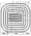
- FIG. 1 is a diagram illustrating a top surface layout of the SiC semiconductor device according to the first embodiment of the present disclosure.
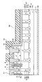
- 2 is a cross-sectional view taken along the line II-II in FIG.
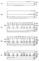
- FIG. 3A to FIG. 3E are cross-sectional views showing manufacturing steps of the SiC semiconductor device shown in FIG. 1 and
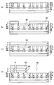
- FIG. 4 (a) to 4 (d) are cross-sectional views showing the manufacturing process of the SiC semiconductor device following FIG. 3 (e)
- FIG. 5A to FIG. 5D are cross-sectional views showing a manufacturing process of the SiC semiconductor device subsequent to FIG.
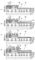
- FIG. 6 (a) to 6 (d) are cross-sectional views showing the manufacturing process of the SiC semiconductor device following FIG. 5 (d)
- FIG. 7 is a diagram illustrating a top surface layout of the SiC semiconductor device according to the second embodiment of the present disclosure.
- 8 is a cross-sectional view taken along the line VIII-VIII in FIG.
- FIG. 9 is a diagram illustrating a top surface layout of the SiC semiconductor device according to the third embodiment of the present disclosure.
- FIG. 10 is an enlarged view of a portion surrounded by an alternate long and short dash line in FIG.
- FIG. 11A to FIG. 11B are diagrams showing an example of a layout in which dents are generated on the surface when the trench J1 is buried by the buried epi technique.
- the SiC semiconductor device shown in FIG. 1 includes a cell region in which a trench gate structure MOSFET is formed as a semiconductor element, and an outer peripheral region (termination structure region) provided with an outer peripheral withstand voltage structure surrounding the cell region. ing.
- FIG. 1 is not a cross-sectional view, hatching is partially shown for easy understanding of the drawing.
- SiC semiconductor device is formed using the n + -type substrate 1 made of SiC, n-type drift layer made of SiC on the main surface of the n + -type substrate 1 2 and p-type base region 3 , And the n + -type source region 4 is grown epitaxially in order.
- the n + type substrate 1 has an n type impurity concentration of, for example, 6.0 ⁇ 10 18 / cm 3 and a thickness of about 300 ⁇ m.
- the n-type impurity concentration is changed between the lower layer portion 2a and the upper layer portion 2b.
- the lower layer portion 2a functions as a dispersion layer that disperses current over a wide range by, for example, 1.0 ⁇ 10 16 / cm 3 and a thickness of 9 ⁇ m, and the upper layer portion 2b has a higher concentration than the lower layer portion.
- the thickness is 0 to 3.0 ⁇ 10 16 / cm 3 and the thickness is 1.9 ⁇ m.
- the p-type base region 3 constitutes a channel epilayer in which a channel region is formed.
- the p-type base region 3 has a p-type impurity concentration of, for example, 2.0 ⁇ 10 17 / cm 3 and a thickness of about 0.5 ⁇ m.
- the n + -type source region 4 has a higher impurity concentration than the n-type drift layer 2, and the n-type impurity concentration in the surface layer portion is, for example, 8.0 ⁇ 10 18 / cm 3 and a thickness of about 0.4 ⁇ m. Yes.
- the p-type base region 3 and the n + -type source region 4 are left on the surface side of the semiconductor substrate.
- the n + -type source region 4 and the p-type base region 3 penetrate through the n-type source region 4.
- a concave portion 20 is formed so as to reach the mold drift layer 2 and has a mesa structure.
- a p-type deep layer 5 extending from the bottom surface of the p-type base region 3 is formed so as to penetrate the upper layer portion 2b of the n-type drift layer 2 and reach the lower layer portion 2a.
- the p-type deep layer 5 has a higher p-type impurity concentration than the p-type base region 3.
- the p-type deep layer 5 includes an upper deep layer (first layer) 5a formed to be embedded in a linear trench (deep trench) 5c formed in the n-type drift layer 2, and A lower deep layer (second layer) 5b formed by ion implantation of p-type impurities into the bottom surface of the trench 5c is configured.
- the extending direction of the p-type deep layer 5 is arbitrary, but extends in the ⁇ 11-20> direction, and both opposing wall surfaces constituting the long side of the trench 5c are the same (1-100) plane As a result, the growth during the buried epitaxy becomes equal on both wall surfaces. For this reason, it is possible to obtain a uniform film quality and to obtain an effect of suppressing embedding defects.
- a plurality of p-type deep layers 5 are arranged in stripes at equal intervals, and the width W1 of the upper deep layer 5a of each p-type deep layer 5 is constant. .
- the upper surface shape of the p-type deep layer 5 is rounded at both longitudinal ends of each deep layer 5.
- the upper deep layer 5a has a p-type impurity concentration of, for example, 6.0 ⁇ 10 17 / cm 3 , a width of 0.7 ⁇ m, and a thickness (depth) of about 1.6 ⁇ m.
- the lower deep layer 5b has a p-type impurity concentration lower than that of the upper deep layer 5a, and is composed of, for example, about 1.0 to 3.0 ⁇ 10 17 / cm 3 and a thickness (depth) of about 0.9 ⁇ m.
- Lower deep p layer 5b can reduce the electric field concentration at the corners of deep p layer 5 by making the impurity concentration lower than that of upper deep p layer, thereby enabling higher breakdown voltage. As shown in FIG.
- the p-type deep layer 5 including the upper deep layer 5a and the lower deep layer 5b is formed from one end to the other end of the cell region.
- the layout extends further to the outside of the cell region than both ends of the trench gate structure.
- the width of the lower deep layer 5b is shown slightly wider than that of the upper deep layer 5a. This is because the p-type impurities are slightly spread by ion implantation and thermal diffusion, but the spread is small compared to Si or the like, and the widths of the lower deep layer 5b and the upper deep layer 5a do not change much.
- a gate trench 6 having a width of, for example, 0.8 ⁇ m and a depth of 1.0 ⁇ m is formed so as to penetrate the p-type base region 3 and the n + -type source region 4 and reach the n-type drift layer 2. .
- the p-type base region 3 and the n + -type source region 4 described above are arranged so as to be in contact with the side surface of the gate trench 6.
- the gate trench 6 is formed in a line-shaped layout in which the horizontal direction in FIG. 2 is the width direction, the vertical direction is the longitudinal direction, and the vertical direction is the depth direction. Further, as shown in FIG. 1, the gate trenches 6 are formed in a stripe shape by arranging a plurality of gate trenches 6 in parallel at equal intervals.
- the same direction as the gate trench 6 is set as the extending direction between the gate trenches 6 or on both sides of the entire gate trench 6, that is, at a position corresponding to the position where the p-type deep layer 5 is formed in the cell region.
- a trench 7 is formed. Since the trenches 7 are disposed between the gate trenches 6 and the like, a plurality of trenches 7 are laid out in a stripe shape. The trench 7 is formed so as to penetrate the n + type source region 4 and reach the p type base region 3. Further, at the bottom of the trench 7, a p + -type contact region 3 a is formed by implanting a p-type impurity into the p-type base region 3.
- the gate insulating film 8 is composed of, for example, a thermal oxide film obtained by thermally oxidizing the inner wall surface of the gate trench 6, and the thickness of the gate insulating film 8 is about 75 nm on both the side and bottom sides of the gate trench 6. Yes. 1 and 2, the corners of the gate insulating film 8 are squared at the bottom and both ends in the longitudinal direction of the gate trench 6, but the rounded shape is obtained by rounding the gate trench 6 in advance. It can also be.
- a gate electrode 9 is formed on the surface of the gate insulating film 8 so as to fill the gate trench 6.
- the gate electrode 9 is made of, for example, Poly-Si doped with impurities.
- a source electrode 11 and a gate wiring are formed on the surface of the n + -type source region 4 and the p + -type contact region 3 a and the surface of the gate electrode 9 via an interlayer insulating film 10.
- the source electrode 11 and the gate wiring are made of a plurality of metals (for example, Ni / Al, etc.), and at least a portion in contact with the n-type SiC (specifically, the n + -type source region 4) is made of n-type SiC.
- the source electrode 11 and the gate wiring are electrically insulated by being formed on the interlayer insulating film 10.
- the source electrode 11 is brought into electrical contact with the p-type base region 3 through the n + -type source region 4 and the p + -type contact region 3a through the contact hole formed in the interlayer insulating film 10, and the gate wiring is connected to the gate. It is in electrical contact with the electrode 9.
- n + -type substrate 1 and electrically connected to the drain electrode 12 are formed on the back side of the n + -type substrate 1 .
- a passivation film 13 is formed on the substrate surface side, and a part of the source electrode 11 and the gate wiring is exposed from the opening provided in the passivation film 13, and this exposed portion is used as a pad to externally.
- the electrical connection can be achieved.
- an n-channel inversion type MOSFET having a trench gate structure is formed.
- a cell region is configured by arranging a plurality of such MOSFETs.
- the mesa structure is formed by forming the recess 20 so as to penetrate the n + -type source region 4 and the p-type base region 3 and reach the n-type drift layer 2. .
- the p-type base region 3 is removed at a position away from the cell region, and the n-type drift layer 2 is exposed.
- the surface layer portion of the n-type drift layer 2 located below the recess 20 is provided with a plurality (four in FIG. 1) of p-type guard ring layers 21 so as to surround the cell region. It has been.
- the p-type guard ring layer 21 has a structure including an upper guard ring 21a embedded in a trench (guard ring trench) 21c and a lower guard ring 21b formed at the bottom thereof.
- Each part constituting the p-type guard ring layer 21 is configured similarly to the above-described p-type deep layer 5, and the upper surface shape of the trench 21 c is a frame-like line shape surrounding the cell region. Although it is different from the trench 5c formed in a line shape, the others are the same.
- the upper guard ring 21a has the same width and the same thickness (depth) as the upper deep layer 5a
- the lower guard ring 21b has the same width and the same thickness (depth) as the lower deep layer 5b.
- the interval between the p-type guard ring layers 21 may be equal, but the electric field concentration is reduced on the inner peripheral side, that is, the cell region side so that the equipotential lines are directed toward the outer peripheral side.
- the interval between the p-type guard ring layers 21 becomes narrower toward the outer peripheral side and narrower at the cell region side.
- the surface layer portion of the n-type drift layer 2 has ap + of about 1.0 ⁇ 10 18 / cm 3 and a thickness (depth) of about 0.9 ⁇ m, for example.
- a mold coupling layer 30 is formed.
- the p + -type coupling layer 30 is located on the outer peripheral region side of the cell region, more specifically, on the outer peripheral region side of all the gate trenches 6 in the p-type deep layer 5.
- the one located on the cell region side of the p-type guard ring layer 21 is connected.
- the boundary position of the recess 20 overlaps with the p + -type coupling layer 30, and the bottom surface of the recess 20 is not the surface of the n-type drift layer 2 but the p + -type coupling layer 30 at this boundary position.
- a portion of the p-type guard ring layer 21 on the cell region side is fixed to the source potential.
- an EQR structure is provided on the outer periphery of the p-type guard ring layer 21 as necessary, thereby forming an outer peripheral region including an outer peripheral pressure-resistant structure surrounding the cell region.
- the SiC semiconductor device concerning this embodiment is comprised by the above structures.
- the channel region is formed on the surface portion of the p-type base region 3 located on the side surface of the gate trench 6 by controlling the voltage applied to the gate electrode 9. To do.
- a current flows between the source electrode 11 and the drain electrode 12 via the n + -type source region 4 and the n-type drift layer 2.
- the p-type deep layer 5 formed to a position deeper than the trench gate structure suppresses the electric field from entering the bottom of the gate trench.
- the electric field concentration is relaxed. Thereby, destruction of the gate insulating film 8 is prevented.
- the p-type guard ring layer 21 is terminated while the equipotential lines are widened toward the outer peripheral direction, and a desired breakdown voltage can be obtained also in the outer peripheral region. Therefore, a SiC semiconductor device capable of obtaining a desired breakdown voltage can be obtained.
- an n + type substrate 1 made of SiC having an n type impurity concentration of, for example, 6.0 ⁇ 10 18 / cm 3 and a thickness of 300 ⁇ m is prepared as a semiconductor substrate.
- a lower layer portion 2a made of SiC having an n-type impurity concentration of 1.0 ⁇ 10 16 / cm 3 and a thickness of 9 ⁇ m is epitaxially grown.
- an upper layer portion made of SiC having a higher concentration than the lower layer portion 2a for example, an n-type impurity concentration of 2.0 to 3.0 ⁇ 10 16 / cm 3 and a thickness of 2.4 ⁇ m. 2b is epitaxially grown.
- Step shown in FIG. 3 (c) An oxide film 40 having a thickness of, for example, about 2 ⁇ m is formed on the upper layer portion 2b. Subsequently, through a photo-etching process using a mask (not shown), the oxide film 40 is patterned to form the formation region of the trench 5c of the p-type deep layer 5 and the trench 21c of the p-type guard ring layer 21 in the oxide film 40. Open. Then, using the patterned oxide film 40 as a mask, the upper layer portion 2a is anisotropically etched by RIE (Reactive Ion Etching) or the like to form trenches 5c and 21c having a width of 0.7 ⁇ m and a depth of 2.1 ⁇ m, for example. To do.
- RIE Reactive Ion Etching
- ion implantation of p-type impurities such as Al is performed in multiple stages in the depth direction and then heat treatment is performed, so that the p-type impurity concentration is, for example, 1.5 to 2.0 ⁇ 10 17 /
- a lower deep layer 5b and a lower guard ring 21b having a thickness of cm 3 and a thickness (depth) of about 0.9 ⁇ m are formed.
- a p-type layer 41 having a p-type impurity concentration of, for example, 6.0 ⁇ 10 17 / cm 3 is formed.
- the p-type layer 41 is also buried in the trenches 5c and 21c by buried epi, but since the trenches 5c and 21c are formed with the same width, a shape is formed on the surface of the p-type layer 41. Abnormality or unevenness can be suppressed. Therefore, the surface of the p-type layer 41 has a flat shape with no irregularities.
- Etchback is performed so that a portion of the p-type layer 41 formed above the surface of the upper layer portion 2b is removed by dry etching. Specifically, over-etching is performed so that the upper layer portion 2b remains about 1.9 ⁇ m. Thereby, the upper deep layer 5a and the upper guard ring 21a are formed. At this time, as described above, since the surface of the p-type layer 41 has a flat shape without unevenness, the surfaces of the upper deep layer 5a, the upper guard ring 21a, and the n-type drift layer 2 are in a flat state. Become. Therefore, a desired gate shape can be obtained when various processes for forming the trench gate structure are performed thereafter.
- an oxide film 42 is formed as a mask on the upper deep layer 5a, the upper guard ring 21a, and the upper layer part 2b, and then the oxide film 42 is patterned through a photoetching process to form the p + -type coupling layer 30. Open in area. Then, ion implantation of a p-type impurity such as Al is performed by using the oxide film 42 as a mask, so that the p-type impurity concentration is about 1.0 ⁇ 10 18 / cm 3 and the thickness (depth) is about 0.9 ⁇ m. A + -type coupling layer 30 is formed.
- the p-type base region 3 having a p-type impurity concentration of, for example, 2.0 ⁇ 10 17 / cm 3 and a thickness of about 0.5 ⁇ m, and the n-type impurity concentration of the surface layer portion is, for example, 8.0.
- An n + -type source region 4 having ⁇ 10 18 / cm 3 and a thickness of about 0.4 ⁇ m is continuously epitaxially grown.
- an oxide film 43 is formed on the n + type source region 4 as a mask. Subsequently, through a photo-etching process using a mask (not shown), the oxide film 43 is patterned to open regions where the gate trench 6 and the recess 20 are to be formed in the oxide film 43. Then, using the patterned oxide film 43 as a mask, the n + -type source region 4, the p-type base region 3 and a part of the n-type drift layer 2 are anisotropically etched by RIE, etc. 20 are formed simultaneously.
- an oxide film 44 is formed as a mask again on the n + type source region 4 including the inside of the gate trench 6 and the recess 20. Subsequently, through a photoetching process using a mask (not shown), the oxide film 44 is patterned to open a region where the trench 7 is to be formed in the oxide film 44. Then, using the patterned oxide film 44 as a mask, the n + -type source region 4 and a part of the p-type base region 3 are anisotropically etched by RIE or the like to form the trench 7.
- p + -type contact regions 3a are formed by performing ion implantation of p-type impurities such as Al in multiple steps in the depth direction while using the oxide film 44 as a mask, followed by heat treatment.
- the gate insulating film 8 made of a thermal oxide film covers the inner wall surface of the gate trench 6 and the surface of the n + -type source region 4.
- Step shown in FIG. 5 (c) After depositing Poly-Si doped with p-type impurities or n-type impurities, this is etched back to leave the Poly-Si at least in the gate trench 6 to form the gate electrode 9.
- an oxide film 45 is formed on the surfaces of the gate electrode 9 and the gate insulating film 8 as a mask. Subsequently, through a photoetching process using a mask (not shown), the oxide film 45 is patterned to open a region corresponding to the trench 7 in the oxide film 45. Then, using the patterned oxide film 45 as a mask, the Poly-Si remaining in the trench 7 is removed.
- An interlayer insulating film 10 made of, for example, an oxide film is formed so as to cover the surfaces of the gate electrode 9 and the gate insulating film 8.
- a resist 46 is formed on the surface of the interlayer insulating film 10 as a mask. Subsequently, through a photo process using a mask (not shown), the resist 46 is exposed to open a region corresponding to the trench 7 in the resist 46. Then, using the patterned resist 46 as a mask, the interlayer insulating film 10 and the gate insulating film 8 formed in the trench 7 are removed.
- Step shown in FIG. 6 (c) An electrode material composed of, for example, a laminated structure of a plurality of metals is formed on the surface of the interlayer insulating film 10 including the inside of the trench 7. Then, the source electrode 11 and the gate wiring are formed by patterning the electrode material. Note that a gate lead-out portion connected to the gate electrode 9 of each cell is provided in a cross section different from that in the figure. A contact hole is opened in the interlayer insulating film 10 at the lead-out portion, so that the gate wiring and the gate electrode 9 are electrically connected.
- Step shown in FIG. 6 (d) After forming the passivation film 13 on the entire surface of the substrate surface, patterning is performed to provide an opening, and the source electrode 11 and the gate wiring are partially exposed.
- the SiC semiconductor device according to the present embodiment is completed.
- the trenches 5c and 21c for forming the p-type deep layer 5 and the p-type guard ring layer 21 are formed with the same width. For this reason, it is possible to suppress the occurrence of irregularities and irregularities on the surface of the p-type layer 41 when the trenches 5c and 21c are buried by buried epi. And since the surface of the p-type layer 41 can be made into a flat shape with no irregularities, in the subsequent steps, the surface is processed from a flat state, and various processes for forming a trench gate structure are performed. Thus, a desired gate shape can be obtained.
- the occurrence of leakage through the gate insulating film 8 can be suppressed, and the electric field relaxation at the bottom of the trench can be performed accurately, and the required life can be satisfied.
- the interval between the p-type guard ring layers 21 is narrower toward the outer peripheral side on the cell region side, and the interval between the upper deep layer 5a and the lower deep layer 5b is set as such.
- the interval between the upper deep layer 5a and the lower deep layer 5b is constant, and the p + -type impurity is formed as a part of the p-type guard ring layer 21.
- the p + -type impurity layer 21d is provided in the surface layer portion of the n-type drift layer 2 so as to overlap each upper deep layer 5a, and the interval between the p + -type impurity layers 21d is narrower on the cell region side and wider as it becomes the outer peripheral side. I have to.
- a p + -type impurity layer 21d is formed by ion-implanting a p-type impurity, and has the same depth and the same impurity concentration.
- the p + -type impurity layer 21 d can be formed simultaneously with the p + -type coupling layer 30.
- p + -type impurity layer 21d by forming simultaneously with the p + -type connecting layer 30 can be formed p + -type impurity layer 21d without adding p + -type impurity layer 21d steps required only for the formation of.
- the p + type guard ring layer 21 is formed not by the upper guard ring 21a formed in the trench 21c or the lower guard ring 21c formed at the bottom of the trench 21c but by the p + type impurity layer 21d separately formed by ion implantation. Can be adjusted. In this way, the interval between the trenches 21 c can be made constant and equal to the interval between the trenches 5.
- the trench formation area is sparsely formed between the cell region where the trench 5c is formed and the outer peripheral region where the trench 21c is formed. For this reason, a dent may occur in the embedded p-type layer 41.
- the interval between the trenches 21c can be made constant and equal to the interval between the trenches 5c, the density of the trench formation area can be suppressed between the cell region and the outer peripheral region. Accordingly, it is possible to further suppress the occurrence of a dent in the p-type layer 41 embedded in the trenches 5c and 21c.
- FIG. 1 A third embodiment of the present disclosure will be described.
- the p-type deep layer 5 and the p-type guard ring layer 21 are connected to the first and second embodiments, and the others are the same as in the first and second embodiments. Therefore, only different parts from the first and second embodiments will be described.
- the case of applying the configuration of the present embodiment to the layout of the first embodiment will be described as an example, but the same can be said for the layout of the second embodiment.
- both longitudinal ends in the longitudinal direction of the p-type deep layer 5 are connected to the p-type guard ring layer 21.
- both longitudinal ends of the p-type deep layer 5 are narrower than the cell region side.
- the connection location of the p-type guard ring layer 21 with the p-type deep layer 5 is narrower than the location that is not the connection location.
- the p-type deep layer 5 is configured by the upper deep layer 5a and the lower deep layer 5b has been described.
- the p-type deep layer 5 is configured only by the upper deep layer 5a. Also good.
- the p-type deep layer 5 is formed to a position deeper than the upper layer portion 2b having a higher impurity concentration than the lower layer portion 2a. May be formed so as to penetrate the upper layer portion 2b.
- the trench 7 is formed and the source electrode 11 is in direct contact with the p-type base region 5.
- the p + -type contact region 3a penetrates the n + -type source region 4 and reaches the p-type base region 3 by, for example, ion implantation of p-type impurities. May be formed.
- the n + -type source region 4 is continuously epitaxially grown on the p-type base region 3, but n-type impurities are ion-implanted at a desired position in the p-type base region 3.
- the n + -type source region 4 may be formed.
- an n-channel type MOSFET in which the first conductivity type is n-type and the second conductivity type is p-type has been described as an example.
- the conductivity type of each component is reversed.
- the present disclosure can be applied to a p-channel type MOSFET.
- the MOSFET has been described as an example of a semiconductor element having a trench gate structure, but the present disclosure can also be applied to an IGBT having a similar trench gate structure.
- the IGBT only changes the conductivity type of the substrate 1 from the n-type to the p-type with respect to the above-described embodiments, and the other structures and manufacturing methods are the same as those of the above-described embodiments.
- the semiconductor device made of SiC has been described as an example.
- the present disclosure can be applied to a semiconductor device made of another semiconductor material such as Si or GaN. Can do.
Landscapes
- Electrodes Of Semiconductors (AREA)
- Recrystallisation Techniques (AREA)
Abstract
半導体装置は、半導体素子を有するセル領域と外周領域とを有する基板(1)と、前記基板の上のドリフト層(2)とを有する。半導体素子は、ベース領域(3)と、ソース領域(4)と、トレンチゲート構造と、ゲートトレンチよりも深いディープ層(5)と、ソース電極(11)と、ドレイン電極(12)と、を備える。外周領域は、前記ドリフト層が露出している凹部(20)と、ガードリング層(21)とを有する、ガードリング層は、露出した前記ドリフト層の表面において、前記セル領域を囲む複数の枠形状とされたガードリングトレンチ(21c)と、ガードリングトレンチ内に配置された第1ガードリング(21a)とを有する。前記ディープトレンチと前記ガードリングトレンチの幅が等しい。
Description
本出願は、2015年5月29日に出願された日本特許出願番号2015-110269号に基づくもので、ここにその記載内容を援用する。
本開示は、ディープ層およびガードリング層を有する半導体装置およびその製造方法に関し、特に炭化珪素(以下、SiCという)半導体装置に関するものである。
従来より、高い電界破壊強度が得られるパワーデバイスの素材としてSiCが注目されている。しかしながら、SiCの破壊電界強度が高いことから、SiCを用いたトレンチゲート構造のMOSFETでは、トレンチ底部のゲート絶縁膜に高電界が掛かり、必要な寿命を満足させられない。このため、トレンチ底部の電界緩和が必要になる。
このようなトレンチ底部の電界緩和が行える構造として、トレンチ底部よりも深いp型ディープ層を備えた構造がある。このような構造とすることで、MOSFETのオフ時にトレンチ底部への電界の入り込みを抑制してトレンチ底部での電界集中を緩和でき、ゲート絶縁膜の破壊を防止することが可能となる。
ところが、SiCでは不純物が拡散し難いことから、イオン注入および不純物の熱拡散によって例えば1μmを超える深さの深いp型ディープ層を形成することは困難である。
このため、非特許文献1に示されるように、深いp型ディープ層を形成する方法として、トレンチ内にp型層を埋め込むようにエピタキシャル成長させる埋込エピ技術が開発されている。このような埋込エピ技術を用いることで、イオン注入や不純物の熱拡散によらずに、例えば1μmを超える深いp型ディープ層を形成することが可能となる。
SiC半導体装置では、セル領域にはp型ディープ層が設けられ、セル領域の外周を囲むように外周耐圧構造が構成される外周領域ではp型ガードリング層が形成される。これらp型ディープ層やp型ガードリング層を共に埋込エピ技術によって形成することができる。
しかしながら、深いp型ディープ層やp型ガードリング層の形成に埋込エピ技術を適用すると、形状異常や表面に凹凸が発生することが確認された。例えば、図11(a)に示すように、トレンチJ1の幅が異なっているために埋め込まれる領域が広がったり、図11(b)に示すようにライン状のトレンチJ1が交差した部分において、形状異常や表面に凹凸が発生した。
このような凹凸が存在した状態で、その後のトレンチゲート形成工程に移行すると、所望のゲート形状を得ることができず、ゲート絶縁膜を通じてのリークが発生したり、トレンチ底部の電界緩和が十分に行えず、必要な寿命を満足させられなくなる。特に、p型ディープ層とp型ガードリング層とを両方共に形成する場合には、それぞれで設計されることから、表面の形状異常や凹凸の発生が起こり易い。
一方、表面の凹凸を無くすために、研削や研磨によって表面を平坦化する方法もあるが、SiCは硬いことから、制御性良く加工することが困難である。したがって、埋込エピが行われるトレンチのパターンを工夫してp型ディープ層の表面の平坦化を実現することが必要である。
なお、ここでは半導体材料としてSiCを用いる場合について説明しているが、SiC以外の半導体材料、例えばSi(シリコン)やGaN(窒化珪素)などが用いられる場合についても、p型ディープ層を埋込エピ技術で形成する場合には同様のことが言える。
Materials Science Forum Vols.600-603(2009)pp171-174、Growth Mechanism and 2D Aluminum Dopant Distribution of Embedded Trench 4H-SiC Region、N.Sugiyama et. al.
本開示は、ディープ層およびガードリング層の表面の平坦化が行え、ゲート絶縁膜を通じてのリークを抑制できる半導体装置およびその製造方法を提供することを目的とする。
本開示の第一の態様において、半導体装置は、セル領域と外周領域とを有する第1または第2導電型の基板と、前記基板の上に形成され、前記基板よりも低不純物濃度とされた第1導電型のドリフト層とを有する。当該セル領域は、半導体素子を有する。半導体素子は、前記ドリフト層の上に形成された第2導電型のベース領域と、前記ベース領域の上に形成され、前記ドリフト層よりも高不純物濃度とされた第1導電型のソース領域と、前記ソース領域の表面から前記ベース領域よりも深くまで形成されたゲートトレンチと、該ゲートトレンチの内壁面に形成されたゲート絶縁膜と、前記ゲート絶縁膜の上に形成されたゲート電極と、を有して構成されたトレンチゲート構造と、前記ドリフト層の表面から前記ゲートトレンチよりも深い位置まで形成された複数のライン状のディープトレンチ内に埋め込まれた第1層を有するディープ層と、前記ソース領域および前記ベース領域に電気的に接続されたソース電極と、前記基板の裏面側に形成されたドレイン電極と、を備える。半導体素子は、前記ゲート電極への印加電圧を制御することで前記ゲートトレンチの側面に位置する前記ベース領域の表面部にチャネル領域を形成し、前記ソース領域および前記ドリフト層を介して、前記ソース電極および前記ドレイン電極の間に電流を流す。前記セル領域の外周を囲む外周領域は、前記ソース領域および前記ベース領域が除去されて、前記ドリフト層が露出している凹部と、ガードリング層とを有する。ガードリング層は、凹部により露出した前記ドリフト層の表面において、前記セル領域を囲む複数の枠形状とされたライン状のガードリングトレンチと、ガードリングトレンチ内に配置され、第2導電型不純物濃度が前記第1層と等しい第2導電型の第1ガードリングとを有する。ライン状とされた前記ディープトレンチと前記ガードリングトレンチの幅が等しくされている。
このように、ディープ層やガードリング層を形成するためのディープトレンチやガードリングトレンチを同じ幅で形成している。このため、埋込エピによって各トレンチを埋め込んだときの第2導電型層の表面の形状異常や凹凸の発生を抑制できる。そして、第2導電型層の表面を凹凸が無い平坦な形状にできることから、その後の工程においても、表面が平坦な状態からの加工となり、トレンチゲート構造を形成するための各種プロセスを行ったときに、所望のゲート形状を得ることが可能となる。したがって、ゲート絶縁膜を通じてのリークの発生を抑制できる。
本開示の第二の態様において、第一の態様に記載の半導体装置の製造方法は、前記基板の主表面上にドリフト層を形成することと、前記ドリフト層の上に前記ディープトレンチおよび前記ガードリングトレンチの形成予定領域が開口するマスクを配置したのち、該マスクを用いて前記ドリフト層をエッチングすることで、前記ディープトレンチおよび前記ガードリングトレンチを同時に形成することと、前記ディープトレンチおよび前記ガードリングトレンチ内を埋め込むように、前記ドリフト層の上に第2導電型不純物層をエピタキシャル成長させることと、前記ドリフト層の上に形成された前記第2導電型不純物層を除去しつつ表面を平坦化することで、前記ディープトレンチ内に前記第1層を形成すると共に前記ガードリングトレンチ内に前記第1ガードリングを形成することと、を含んでいる。
上記の半導体装置の製造方法において、埋込エピによって各トレンチを埋め込んだときの第2導電型層の表面の形状異常や凹凸の発生を抑制できる。そして、第2導電型層の表面を凹凸が無い平坦な形状にできることから、その後の工程においても、表面が平坦な状態からの加工となり、トレンチゲート構造を形成するための各種プロセスを行ったときに、所望のゲート形状を得ることが可能となる。したがって、ゲート絶縁膜を通じてのリークの発生を抑制できる。
本開示についての上記目的およびその他の目的、特徴や利点は、添付の図面を参照しながら下記の詳細な記述により、より明確になる。その図面は、
図1は、本開示の第1実施形態にかかるSiC半導体装置の上面レイアウトを示す図であり、
図2は、図1のII-II断面図であり、
図3(a)から図3(e)は、図1および図2に示すSiC半導体装置の製造工程を示した断面図であり、
図4(a)から図4(d)は、図3(e)に続くSiC半導体装置の製造工程を示した断面図であり、
図5(a)から図5(d)は、図4(d)に続くSiC半導体装置の製造工程を示した断面図であり、
図6(a)から図6(d)は、図5(d)に続くSiC半導体装置の製造工程を示した断面図であり、
図7は、本開示の第2実施形態にかかるSiC半導体装置の上面レイアウトを示す図であり、
図8は、図7のVIII-VIII断面図であり、
図9は、本開示の第3実施形態にかかるSiC半導体装置の上面レイアウトを示す図であり、
図10は、図9中の一点鎖線で囲んだ部分の拡大図であり、
図11(a)から図11(b)は、トレンチJ1を埋込エピ技術で埋め込んだときに表面に凹みが発生するレイアウトの一例を示した図である。
以下、本開示の実施形態について図に基づいて説明する。なお、以下の各実施形態相互において、互いに同一もしくは均等である部分には、同一符号を付して説明を行う。
(第1実施形態)
本開示の第1実施形態について説明する。ここではトレンチゲート構造のMOSFETとして反転型のMOSFETが形成されたSiC半導体装置を例に挙げて説明する。
本開示の第1実施形態について説明する。ここではトレンチゲート構造のMOSFETとして反転型のMOSFETが形成されたSiC半導体装置を例に挙げて説明する。
図1に示すSiC半導体装置は、半導体素子としてトレンチゲート構造のMOSFETが形成されるセル領域とこのセル領域を囲む外周耐圧構造が備えられた外周領域(終端構造領域)とを有した構成とされている。なお、図1は断面図ではないが、図を見やすくするために部分的にハッチングを示してある。
図2に示すように、SiC半導体装置は、SiCからなるn+型基板1を用いて形成され、n+型基板1の主表面上にSiCからなるn型ドリフト層2とp型ベース領域3、および、n+型ソース領域4が順にエピタキシャル成長させられている。
n+型基板1は、n型不純物濃度が例えば6.0×10¹⁸/cm3とされ、厚さが300μm程度とされている。n型ドリフト層2は、下層部2aと上層部2bとでn型不純物濃度が変えられている。下層部2aは、例えば1.0×1016/cm3で厚さ9μm、上層部2bは下層部よりも高濃度とされることで電流を広範囲に分散させる分散層として機能し、例えば2.0~3.0×1016/cm3で厚さ1.9μmとされている。
また、p型ベース領域3は、チャネル領域が形成されるチャネルエピ層を構成するもので、p型不純物濃度が例えば2.0×10¹⁷/cm3、厚さ0.5μm程度で構成されている。n+型ソース領域4は、n型ドリフト層2よりも高不純物濃度とされ、表層部におけるn型不純物濃度が例えば8.0×1018/cm3、厚さ0.4μm程度で構成されている。
セル領域では、半導体基板の表面側においてp型ベース領域3およびn+型ソース領域4が残されており、外周領域では、これらn+型ソース領域4およびp型ベース領域3を貫通してn型ドリフト層2に達するように凹部20が形成され、メサ構造とされている。
また、セル領域では、n型ドリフト層2のうちの上層部2bを貫通して下層部2aに達するように、p型ベース領域3の底面から伸びるp型ディープ層5が形成されている。p型ディープ層5は、p型ベース領域3よりもp型不純物濃度が高くされている。具体的には、p型ディープ層5は、n型ドリフト層2に形成されたライン状のトレンチ(ディープトレンチ)5c内に埋め込まれるように形成された上部ディープ層(第1層)5aと、トレンチ5cの底面に対してp型不純物がイオン注入されて形成された下部ディープ層(第2層)5bとを有して構成されている。p型ディープ層5の延設方向については任意であるが、<11-20>方向に延びており、トレンチ5cのうち長辺を構成している対向する両壁面が同じ(1-100)面となるようにすると、埋込エピ時の成長が両壁面で等しくなる。このため、均一な膜質にできると共に、埋込み不良の抑制効果も得られる。
p型ディープ層5は、図1に示すように、複数本が等間隔にストライプ状に配置されており、各p型ディープ層5のうちの上部ディープ層5aの幅W1は一定とされている。また、図1に示すように、各ディープ層5における長手方向の両端では、p型ディープ層5の上面形状が丸められている。
上部ディープ層5aは、p型不純物濃度が例えば6.0×10¹⁷/cm3、幅0.7μm、厚さ(深さ)1.6μm程度で構成されている。下部ディープ層5bは、p型不純物濃度が上部ディープ層5aより低くされ、例えば1.0~3.0×1017/cm3、厚さ(深さ)0.9μm程度で構成されている。下部ディープp層5bは、上部ディープp層より不純物濃度を低くすることにより、ディープp層5の角部の電界集中を緩和でき、より高耐圧化が可能となる。これら上部ディープ層5aおよび下部ディープ層5bを含むp型ディープ層5は、図1に示すようにセル領域の一端から他端に渡って形成されている。そして、後述するトレンチゲート構造と同方向を長手方向として延設されているが、トレンチゲート構造の両端よりも更にセル領域の外側まで延設されたレイアウトとされている。
なお、図2では、下部ディープ層5bの幅は、上部ディープ層5aよりも若干広く示してある。これは、イオン注入および熱拡散によってp型不純物が若干広がるためであるが、Siなどと比較すると広がりは小さく、下部ディープ層5bと上部ディープ層5aの幅はあまり変わらない。
また、p型ベース領域3およびn+型ソース領域4を貫通してn型ドリフト層2に達するように、例えば幅が0.8μm、深さが1.0μmのゲートトレンチ6が形成されている。このゲートトレンチ6の側面と接するように上述したp型ベース領域3およびn+型ソース領域4が配置されている。ゲートトレンチ6は、図2の紙面左右方向を幅方向、紙面垂直方向を長手方向、紙面上下方向を深さ方向とするライン状のレイアウトで形成されている。また、図1に示すように、ゲートトレンチ6は、複数本が平行に等間隔で並べられることでストライプ状とされている。
また、各ゲートトレンチ6の間や全ゲートトレンチ6を挟んだ両側、つまりセル領域においてp型ディープ層5が形成された位置と対応する位置に、ゲートトレンチ6と同方向を延設方向とするトレンチ7が形成されている。トレンチ7は、ゲートトレンチ6の間などに配置されているため、複数本がストライプ状にレイアウトされている。このトレンチ7は、n+型ソース領域4を貫通してp型ベース領域3に達するように形成されている。さらに、トレンチ7の底部において、p型ベース領域3にはp型不純物が注入されることによってp+型コンタクト領域3aが形成されている。
さらに、ゲートトレンチ6の内壁面はゲート絶縁膜8にて覆われている。ゲート絶縁膜8は、例えばゲートトレンチ6の内壁面を熱酸化した熱酸化膜などによって構成されており、ゲート絶縁膜8の厚みはゲートトレンチ6の側面側と底部側共に例えば75nm程度となっている。図1および図2では、ゲートトレンチ6の底部および長手方向両端においてゲート絶縁膜8の角部が角張った形状となっているが、予めゲートトレンチ6を丸め処理しておくことで丸まった形状となるようにもできる。
そして、このゲート絶縁膜8の表面において、ゲートトレンチ6を埋め込むようにゲート電極9が形成されている。ゲート電極9は、例えば不純物がドープされたPoly-Siによって構成されている。
また、n+型ソース領域4およびp+型コンタクト領域3aの表面やゲート電極9の表面には、層間絶縁膜10を介してソース電極11やゲート配線(図示せず)が形成されている。ソース電極11およびゲート配線は、複数の金属(例えばNi/Al等)にて構成されており、少なくともn型SiC(具体的にはn+型ソース領域4)と接触する部分はn型SiCとオーミック接触可能な金属で構成され、少なくともp型SiC(具体的にはp+型コンタクト領域3a)と接触する部分はp型SiCとオーミック接触可能な金属で構成されている。なお、これらソース電極11およびゲート配線は、層間絶縁膜10上に形成されることで電気的に絶縁されている。そして、層間絶縁膜10に形成されたコンタクトホールを通じてソース電極11はn+型ソース領域4やp+型コンタクト領域3aを介してp型ベース領域3と電気的に接触させられ、ゲート配線はゲート電極9と電気的に接触させられている。
さらに、n+型基板1の裏面側にはn+型基板1と電気的に接続されたドレイン電極12が形成されている。そして、基板表面側にパッシベーション膜13が形成されており、パッシベーション膜13に設けられた開口部より、ソース電極11やゲート配線の一部が露出させられており、この露出部分をパッドとして外部との電気的接続が図れるようにされている。このような構造により、nチャネルタイプの反転型のトレンチゲート構造のMOSFETが構成されている。そして、このようなMOSFETが複数セル配置されることでセル領域が構成されている。
一方、外周領域では、上記したように、n+型ソース領域4およびp型ベース領域3を貫通してn型ドリフト層2に達するように凹部20が形成されることでメサ構造とされている。このため、セル領域から離れた位置ではp型ベース領域3が除去され、n型ドリフト層2が露出させられている。
また、凹部20の下方に位置するn型ドリフト層2の表層部には、セル領域を囲むように、複数本(図1中では4本記載してある)のp型ガードリング層21が備えられている。p型ガードリング層21は、トレンチ(ガードリングトレンチ)21c内に埋め込まれた上部ガードリング21aとその底部に形成された下部ガードリング21bとを備えた構造となっている。p型ガードリング層21を構成する各部は、上記したp型ディープ層5と同様の構成とされており、トレンチ21cの上面形状がセル領域を囲む枠形状のライン状とされている点において、ライン状に形成されたトレンチ5cと異なっているが、他は同様である。すなわち、上部ガードリング21aは上部ディープ層5aと同様の幅、同様の厚さ(深さ)とされ、下部ガードリング21bは下部ディープ層5bと同様の幅、同様の厚さ(深さ)とされている。また、各p型ガードリング層21の間隔については、等間隔であっても良いが、より内周側、つまりセル領域側において電界集中を緩和して等電位線がより外周側に向かうように、p型ガードリング層21の間隔がセル領域側で狭く外周側になるほど広くされている。
さらに、セル領域のうち外周領域の近傍から外周領域にかけて、n型ドリフト層2の表層部には、例えば1.0×10¹⁸/cm3、厚さ(深さ)0.9μm程度のp+型連結層30が形成されている。p+型連結層30は、セル領域のうち外周領域側に位置しているp型ディープ層5、より詳しくはp型ディープ層5のうち全ゲートトレンチ6よりも外周領域側に位置しているものとp型ガードリング層21のうちの最もセル領域側に位置しているものとを連結する。これにより、凹部20の境界位置(メサ構造の境界位置)がp+型連結層30と重なり、この境界位置において凹部20の底面がn型ドリフト層2の表面ではなくp+型連結層30によって構成された構造とされ、かつ、p型ガードリング層21のうちのセル領域側の部分がソース電位に固定されている。
そして、図示していないが、必要に応じてp型ガードリング層21よりも外周にEQR構造が備えられることにより、セル領域を囲む外周耐圧構造が備えられた外周領域が構成されている。
以上のような構造により、本実施形態にかかるSiC半導体装置が構成されている。このように構成されるSiC半導体装置は、MOSFETをオンするときには、ゲート電極9への印加電圧を制御することでゲートトレンチ6の側面に位置するp型ベース領域3の表面部にチャネル領域を形成する。これにより、n+型ソース領域4およびn型ドリフト層2を介して、ソース電極11およびドレイン電極12の間に電流を流す。
そして、MOSFETのオフ時には、高電圧が印加されたとしても、トレンチゲート構造よりも深い位置まで形成されたp型ディープ層5によってゲートトレンチ底部への電界の入り込みが抑制されて、ゲートトレンチ底部での電界集中が緩和される。これにより、ゲート絶縁膜8の破壊が防止される。また、外周領域では、p型ガードリング層21によって等電位線の間隔が外周方向に向かって広がりながら終端させられるようになり、外周領域においても所望の耐圧を得ることができる。したがって、所望の耐圧を得ることが可能なSiC半導体装置とすることができる。
続いて、本実施形態に係るSiC半導体装置の製造方法について図3(a)~図6(d)を参照して説明する。
〔図3(a)に示す工程〕
まず、半導体基板として、n型不純物濃度が例えば6.0×10¹⁸/cm3とされ、厚さが300μmのSiCからなるn+型基板1を用意する。このn+型基板1の主表面上に、例えばn型不純物濃度が1.0×1016/cm3で厚さ9μmのSiCからなる下層部2aをエピタキシャル成長させる。
まず、半導体基板として、n型不純物濃度が例えば6.0×10¹⁸/cm3とされ、厚さが300μmのSiCからなるn+型基板1を用意する。このn+型基板1の主表面上に、例えばn型不純物濃度が1.0×1016/cm3で厚さ9μmのSiCからなる下層部2aをエピタキシャル成長させる。
〔図3(b)に示す工程〕
次に、下層部2aの表面上に、下層部2aよりも高濃度、例えばn型不純物濃度が2.0~3.0×10¹⁶/cm3で厚さ2.4μmのSiCからなる上層部2bをエピタキシャル成長させる。
次に、下層部2aの表面上に、下層部2aよりも高濃度、例えばn型不純物濃度が2.0~3.0×10¹⁶/cm3で厚さ2.4μmのSiCからなる上層部2bをエピタキシャル成長させる。
〔図3(c)に示す工程〕
上層部2bの上に例えば2μm程度の膜厚の酸化膜40を成膜する。続いて、図示しないマスクを用いたフォトエッチング工程を経て、酸化膜40をパターニングして酸化膜40のうちのp型ディープ層5のトレンチ5cおよびp型ガードリング層21のトレンチ21cの形成予定領域を開口させる。そして、パターニング後の酸化膜40をマスクとして用いて、上層部2aをRIE(Reactive Ion Etching)などによって異方性エッチングし、例えば幅0.7μm、深さ2.1μmのトレンチ5c、21cを形成する。
上層部2bの上に例えば2μm程度の膜厚の酸化膜40を成膜する。続いて、図示しないマスクを用いたフォトエッチング工程を経て、酸化膜40をパターニングして酸化膜40のうちのp型ディープ層5のトレンチ5cおよびp型ガードリング層21のトレンチ21cの形成予定領域を開口させる。そして、パターニング後の酸化膜40をマスクとして用いて、上層部2aをRIE(Reactive Ion Etching)などによって異方性エッチングし、例えば幅0.7μm、深さ2.1μmのトレンチ5c、21cを形成する。
〔図3(d)に示す工程〕
酸化膜40をマスクとしたままAlなどのp型不純物のイオン注入を深さ方向において多段階に行ったのち熱処理することで、p型不純物濃度が例えば1.5~2.0×10¹⁷/cm3、厚さ(深さ)0.9μm程度の下部ディープ層5bおよび下部ガードリング21bを形成する。
酸化膜40をマスクとしたままAlなどのp型不純物のイオン注入を深さ方向において多段階に行ったのち熱処理することで、p型不純物濃度が例えば1.5~2.0×10¹⁷/cm3、厚さ(深さ)0.9μm程度の下部ディープ層5bおよび下部ガードリング21bを形成する。
〔図3(e)に示す工程〕
酸化膜40を除去した後、p型不純物濃度が例えば6.0×10¹⁷/cm3のp型層41を成膜する。このとき、埋込エピにより、トレンチ5c、21c内にもp型層41が埋め込まれることになるが、トレンチ5c、21cを同じ幅で形成していることから、p型層41の表面に形状異常が発生したり凹凸が発生することを抑制できる。したがって、p型層41の表面は凹凸が無い平坦な形状となる。
酸化膜40を除去した後、p型不純物濃度が例えば6.0×10¹⁷/cm3のp型層41を成膜する。このとき、埋込エピにより、トレンチ5c、21c内にもp型層41が埋め込まれることになるが、トレンチ5c、21cを同じ幅で形成していることから、p型層41の表面に形状異常が発生したり凹凸が発生することを抑制できる。したがって、p型層41の表面は凹凸が無い平坦な形状となる。
〔図4(a)に示す工程〕
ドライエッチングによってp型層41のうち上層部2bの表面より上に形成された部分がなくなるようにエッチバックする。具体的には、上層部2bが1.9μm程度残るようにオーバエッチングを行う。これにより、上部ディープ層5aや上部ガードリング21aが形成される。このとき、上記したように、p型層41の表面が凹凸の無い平坦な形状となっていることから、上部ディープ層5aや上部ガードリング21aおよびn型ドリフト層2の表面は平坦な状態となる。したがって、この後にトレンチゲート構造を形成するための各種プロセスを行ったときに、所望のゲート形状を得ることが可能となる。
ドライエッチングによってp型層41のうち上層部2bの表面より上に形成された部分がなくなるようにエッチバックする。具体的には、上層部2bが1.9μm程度残るようにオーバエッチングを行う。これにより、上部ディープ層5aや上部ガードリング21aが形成される。このとき、上記したように、p型層41の表面が凹凸の無い平坦な形状となっていることから、上部ディープ層5aや上部ガードリング21aおよびn型ドリフト層2の表面は平坦な状態となる。したがって、この後にトレンチゲート構造を形成するための各種プロセスを行ったときに、所望のゲート形状を得ることが可能となる。
〔図4(b)に示す工程〕
上部ディープ層5aや上部ガードリング21aおよび上層部2bの上にマスクとして例えば酸化膜42を成膜したのち、フォトエッチング工程を経て、酸化膜42をパターニングし、p+型連結層30の形成予定領域において開口させる。そして、酸化膜42をマスクとしてAlなどのp型不純物のイオン注入を行うことで、p型不純物濃度が例えば1.0×10¹⁸/cm3、厚さ(深さ)0.9μm程度のp+型連結層30を形成する。
上部ディープ層5aや上部ガードリング21aおよび上層部2bの上にマスクとして例えば酸化膜42を成膜したのち、フォトエッチング工程を経て、酸化膜42をパターニングし、p+型連結層30の形成予定領域において開口させる。そして、酸化膜42をマスクとしてAlなどのp型不純物のイオン注入を行うことで、p型不純物濃度が例えば1.0×10¹⁸/cm3、厚さ(深さ)0.9μm程度のp+型連結層30を形成する。
〔図4(c)に示す工程〕
酸化膜42を除去した後、p型不純物濃度が例えば2.0×10¹⁷/cm3、厚さ0.5μm程度のp型ベース領域3と、表層部におけるn型不純物濃度が例えば8.0×1018/cm3、厚さ0.4μm程度のn+型ソース領域4を連続してエピタキシャル成長させる。
酸化膜42を除去した後、p型不純物濃度が例えば2.0×10¹⁷/cm3、厚さ0.5μm程度のp型ベース領域3と、表層部におけるn型不純物濃度が例えば8.0×1018/cm3、厚さ0.4μm程度のn+型ソース領域4を連続してエピタキシャル成長させる。
〔図4(d)に示す工程〕
n+型ソース領域4の上にマスクとして例えば酸化膜43を成膜する。続いて、図示しないマスクを用いたフォトエッチング工程を経て、酸化膜43をパターニングして酸化膜43のうちのゲートトレンチ6および凹部20の形成予定領域を開口させる。そして、パターニング後の酸化膜43をマスクとして用いて、n+型ソース領域4やp型ベース領域3およびn型ドリフト層2の一部をRIEなどによって異方性エッチングし、ゲートトレンチ6および凹部20を同時に形成する。
n+型ソース領域4の上にマスクとして例えば酸化膜43を成膜する。続いて、図示しないマスクを用いたフォトエッチング工程を経て、酸化膜43をパターニングして酸化膜43のうちのゲートトレンチ6および凹部20の形成予定領域を開口させる。そして、パターニング後の酸化膜43をマスクとして用いて、n+型ソース領域4やp型ベース領域3およびn型ドリフト層2の一部をRIEなどによって異方性エッチングし、ゲートトレンチ6および凹部20を同時に形成する。
〔図5(a)に示す工程〕
酸化膜43を除去した後、ゲートトレンチ6および凹部20内を含めてn+型ソース領域4の上に再びマスクとして例えば酸化膜44を成膜する。続いて、図示しないマスクを用いたフォトエッチング工程を経て、酸化膜44をパターニングして酸化膜44のうちのトレンチ7の形成予定領域を開口させる。そして、パターニング後の酸化膜44をマスクとして用いて、n+型ソース領域4やp型ベース領域3の一部をRIEなどによって異方性エッチングし、トレンチ7を形成する。
酸化膜43を除去した後、ゲートトレンチ6および凹部20内を含めてn+型ソース領域4の上に再びマスクとして例えば酸化膜44を成膜する。続いて、図示しないマスクを用いたフォトエッチング工程を経て、酸化膜44をパターニングして酸化膜44のうちのトレンチ7の形成予定領域を開口させる。そして、パターニング後の酸化膜44をマスクとして用いて、n+型ソース領域4やp型ベース領域3の一部をRIEなどによって異方性エッチングし、トレンチ7を形成する。
さらに、酸化膜44をマスクとしたままAlなどのp型不純物のイオン注入を深さ方向において多段階に行ったのち熱処理することで、p+型コンタクト領域3aを形成する。
〔図5(b)に示す工程〕
例えば熱酸化工程を行うことによって、熱酸化膜により構成されるゲート絶縁膜8によってゲートトレンチ6の内壁面上およびn+型ソース領域4の表面上を覆う。
例えば熱酸化工程を行うことによって、熱酸化膜により構成されるゲート絶縁膜8によってゲートトレンチ6の内壁面上およびn+型ソース領域4の表面上を覆う。
〔図5(c)に示す工程〕
p型不純物もしくはn型不純物がドープされたPoly-Siをデポジションした後、これをエッチバックし、少なくともゲートトレンチ6内にPoly-Siを残すことでゲート電極9を形成する。
p型不純物もしくはn型不純物がドープされたPoly-Siをデポジションした後、これをエッチバックし、少なくともゲートトレンチ6内にPoly-Siを残すことでゲート電極9を形成する。
〔図5(d)に示す工程〕
ゲート電極9およびゲート絶縁膜8の表面上にマスクとして例えば酸化膜45を成膜する。続いて、図示しないマスクを用いたフォトエッチング工程を経て、酸化膜45をパターニングして酸化膜45のうちのトレンチ7と対応する領域を開口させる。そして、パターニング後の酸化膜45をマスクとして用いて、トレンチ7内に残っていたPoly-Siを除去する。
ゲート電極9およびゲート絶縁膜8の表面上にマスクとして例えば酸化膜45を成膜する。続いて、図示しないマスクを用いたフォトエッチング工程を経て、酸化膜45をパターニングして酸化膜45のうちのトレンチ7と対応する領域を開口させる。そして、パターニング後の酸化膜45をマスクとして用いて、トレンチ7内に残っていたPoly-Siを除去する。
〔図6(a)に示す工程〕
ゲート電極9およびゲート絶縁膜8の表面を覆うように、例えば酸化膜などによって構成される層間絶縁膜10を形成する。
ゲート電極9およびゲート絶縁膜8の表面を覆うように、例えば酸化膜などによって構成される層間絶縁膜10を形成する。
〔図6(b)に示す工程〕
層間絶縁膜10の表面上にマスクとして例えばレジスト46を成膜する。続いて、図示しないマスクを用いたフォト工程を経て、レジスト46を露光してレジスト46のうちのトレンチ7と対応する領域を開口させる。そして、パターニング後のレジスト46をマスクとして用いて、トレンチ7内に形成されている層間絶縁膜10およびゲート絶縁膜8を除去する。
層間絶縁膜10の表面上にマスクとして例えばレジスト46を成膜する。続いて、図示しないマスクを用いたフォト工程を経て、レジスト46を露光してレジスト46のうちのトレンチ7と対応する領域を開口させる。そして、パターニング後のレジスト46をマスクとして用いて、トレンチ7内に形成されている層間絶縁膜10およびゲート絶縁膜8を除去する。
〔図6(c)に示す工程〕
トレンチ7内を含めて、層間絶縁膜10の表面上に例えば複数の金属の積層構造により構成される電極材料を形成する。そして、電極材料をパターニングすることで、ソース電極11およびゲート配線を形成する。なお、本図とは異なる断面において各セルのゲート電極9に繋がるゲート引出部が設けられている。その引出部において層間絶縁膜10にコンタクトホールが開けられることで、ゲート配線とゲート電極9との電気的接続が行われるようになっている。
トレンチ7内を含めて、層間絶縁膜10の表面上に例えば複数の金属の積層構造により構成される電極材料を形成する。そして、電極材料をパターニングすることで、ソース電極11およびゲート配線を形成する。なお、本図とは異なる断面において各セルのゲート電極9に繋がるゲート引出部が設けられている。その引出部において層間絶縁膜10にコンタクトホールが開けられることで、ゲート配線とゲート電極9との電気的接続が行われるようになっている。
〔図6(d)に示す工程〕
基板表面側の全面にパッシベーション膜13を成膜したのち、パターニングして開口部を設け、部分的にソース電極11やゲート配線を露出させる。
基板表面側の全面にパッシベーション膜13を成膜したのち、パターニングして開口部を設け、部分的にソース電極11やゲート配線を露出させる。
この後の工程については図示しないが、n+型基板1の裏面側にドレイン電極12を形成することで、本実施形態にかかるSiC半導体装置が完成する。
以上説明したように、本実施形態では、p型ディープ層5やp型ガードリング層21を形成するためのトレンチ5c、21cを同じ幅で形成している。このため、埋込エピによってトレンチ5c、21cを埋め込んだときのp型層41の表面の形状異常や凹凸の発生を抑制できる。そして、p型層41の表面を凹凸が無い平坦な形状にできることから、その後の工程においても、表面が平坦な状態からの加工となり、トレンチゲート構造を形成するための各種プロセスを行ったときに、所望のゲート形状を得ることが可能となる。
したがって、ゲート絶縁膜8を通じてのリークの発生を抑制できると共に、トレンチ底部の電界緩和を的確に行うことが可能となって、必要な寿命を満足させることが可能となる。
(第2実施形態)
本開示の第2実施形態について説明する。本実施形態は、第1実施形態に対してp型ガードリング層21の構成を変更したものであり、その他については第1実施形態と同様であるため、第1実施形態と異なる部分についてのみ説明する。
本開示の第2実施形態について説明する。本実施形態は、第1実施形態に対してp型ガードリング層21の構成を変更したものであり、その他については第1実施形態と同様であるため、第1実施形態と異なる部分についてのみ説明する。
上記第1実施形態では、p型ガードリング層21の間隔がセル領域側で狭く外周側になるほど広くしてあり、上部ディープ層5aおよび下部ディープ層5bの間隔をそのように設定してある。これに対して、図7および図8に示すように、本実施形態では、上部ディープ層5aおよび下部ディープ層5bの間隔については一定とし、p型ガードリング層21の一部としてp+型不純物層21dを設けることで、同様の構造を構成している。すなわち、各上部ディープ層5aと重なるようにn型ドリフト層2の表層部にp+型不純物層21dを備え、p+型不純物層21dの間隔がセル領域側で狭く外周側になるほど広くなるようにしている。このようなp+型不純物層21dは、p型不純物をイオン注入することによって形成され、同じ深さ同じ不純物濃度とされている。例えば、p+型不純物層21dをp+型連結層30と同時に形成することが可能である。p+型不純物層21dをp+型連結層30と同時に形成することで、p+型不純物層21dの形成のみに必要な工程を追加することなくp+型不純物層21dを形成できる。
このように、トレンチ21c内に形成される上部ガードリング21aやトレンチ21cの底部に形成される下部ガードリング21cではなく、イオン注入によって別途形成できるp+型不純物層21dによってp型ガードリング層21の間隔を調整できる。そして、このようにすれば、トレンチ21cの間隔については一定にし、トレンチ5の間隔と等しくすることができる。
例えば、第1実施形態のようにトレンチ21cの間隔が異なっている場合、トレンチ5cが形成されたセル領域とトレンチ21cが形成された外周領域との間においてトレンチ形成面積に疎密が発生する。このため、埋め込まれるp型層41に凹みが発生する可能性がある。しかしながら、本実施形態のようにすれば、トレンチ21cの間隔を一定としてトレンチ5cの間隔と等しくできることから、セル領域と外周領域とでトレンチ形成面積の疎密を抑制できる。したがって、トレンチ5c、21cに埋め込まれるp型層41に凹みが発生することをより抑制することが可能となる。
(第3実施形態)
本開示の第3実施形態について説明する。本実施形態は、第1、第2実施形態に対してp型ディープ層5とp型ガードリング層21とを接続するようにしたものであり、その他については第1、第2実施形態と同様であるため、第1、第2実施形態と異なる部分についてのみ説明する。なお、ここでは第1実施形態のレイアウトに対して本実施形態の構成を適用する場合を例に挙げて説明するが、第2実施形態のレイアウトに対しても同様のことが言える。
本開示の第3実施形態について説明する。本実施形態は、第1、第2実施形態に対してp型ディープ層5とp型ガードリング層21とを接続するようにしたものであり、その他については第1、第2実施形態と同様であるため、第1、第2実施形態と異なる部分についてのみ説明する。なお、ここでは第1実施形態のレイアウトに対して本実施形態の構成を適用する場合を例に挙げて説明するが、第2実施形態のレイアウトに対しても同様のことが言える。
図9に示すように、本実施形態では、p型ディープ層5の長手方向両端がp型ガードリング層21に接続されるようにしている。ただし、p型ディープ層5とp型ガードリング層21との接続箇所において、埋め込まれる領域が広がらないようにする必要がある。このため、本実施形態では、図10に示すように、p型ディープ層5の長手方向両端がそれよりもセル領域側よりも幅狭となるようにしてある。同様に、p型ガードリング層21のうちのp型ディープ層5との接続箇所が接続箇所ではない場所よりも幅狭となるようにしてある。
このような構成とすることで、p型ディープ層5とp型ガードリング層21とが接続される構造においても、第1実施形態と同様の効果を得ることができる。
(他の実施形態)
(1)例えば、上記各実施形態では、p型ディープ層5を上部ディープ層5aと下部ディープ層5bにより構成する場合について説明したが、p型ディープ層5を上部ディープ層5aのみで構成しても良い。その場合、電界の入り込みを抑制するために、下層部2aと比べて高不純物濃度とされた上層部2bよりもp型ディープ層5が深い位置まで形成されているのが好ましいことから、トレンチ5cが上層部2bを貫通するように形成すると良い。
(1)例えば、上記各実施形態では、p型ディープ層5を上部ディープ層5aと下部ディープ層5bにより構成する場合について説明したが、p型ディープ層5を上部ディープ層5aのみで構成しても良い。その場合、電界の入り込みを抑制するために、下層部2aと比べて高不純物濃度とされた上層部2bよりもp型ディープ層5が深い位置まで形成されているのが好ましいことから、トレンチ5cが上層部2bを貫通するように形成すると良い。
(2)上記各実施形態では、p型ベース領域3をソース電極11と接続するために、トレンチ7を形成してソース電極11が直接p型ベース領域5と接するような構造とした。しかしながら、このような構成も一例を示したに過ぎず、例えばp型不純物のイオン注入等によって、n+型ソース領域4を貫通してp型ベース領域3に達するようにp+型コンタクト領域3aを形成しても良い。
(3)上記各実施形態では、p型ベース領域3の上にn+型ソース領域4を連続してエピタキシャル成長させて形成したが、p型ベース領域3の所望位置にn型不純物をイオン注入することでn+型ソース領域4を形成しても良い。
(4)上記第1、第2実施形態では、p型ディープ層5のうちの長手方向両端が丸まった形状である場合について説明したが、先端が尖った三角形状、先端が平面とされた四角形状であっても良い。三角形状とする場合、p型ディープ層5の延設方向が<11-20>方向であると、SiCのような六方晶においては、三角形状とされる先端の2辺を構成する壁面の面方位が共に等価な(1-100)面となり易い。したがって、等価な面それぞれでの埋込エピ時の成長が等しくなり、均一な膜質にできると共に埋込不良の抑制効果も得られる。
(5)上記各実施形態では、第1導電型をn型、第2導電型をp型としたnチャネルタイプのMOSFETを例に挙げて説明したが、各構成要素の導電型を反転させたpチャネルタイプのMOSFETに対しても本開示を適用することができる。さらに、上記説明では、トレンチゲート構造の半導体素子としてMOSFETを例に挙げて説明したが、同様のトレンチゲート構造のIGBTに対しても本開示を適用することができる。IGBTは、上記各実施形態に対して基板1の導電型をn型からp型に変更するだけであり、その他の構造や製造方法に関しては上記各実施形態と同様である。
(6)上記各実施形態では、SiCで構成される半導体装置を例に挙げて説明したが、他の半導体材料、例えばSiやGaNなどで構成される半導体装置についても、本開示を適用することができる。
(7)なお、結晶の方位を示す場合、本来ならば所望の数字の上にバー(-)を付すべきであるが、電子出願に基づく表現上の制限が存在するため、本明細書においては、所望の数字の前にバーを付すものとする。
本開示は、実施例に準拠して記述されたが、本開示は当該実施例や構造に限定されるものではないと理解される。本開示は、様々な変形例や均等範囲内の変形をも包含する。加えて、様々な組み合わせや形態、さらには、それらに一要素のみ、それ以上、あるいはそれ以下、を含む他の組み合わせや形態をも、本開示の範疇や思想範囲に入るものである。
Claims (11)
- セル領域と外周領域とを有する第1または第2導電型の基板(1)と、
前記基板の上に形成され、前記基板よりも低不純物濃度とされた第1導電型のドリフト層(2)とを有し、
当該セル領域は、半導体素子を有し、
半導体素子は、
前記ドリフト層の上に形成された第2導電型のベース領域(3)と、
前記ベース領域の上に形成され、前記ドリフト層よりも高不純物濃度とされた第1導電型のソース領域(4)と、
前記ソース領域の表面から前記ベース領域よりも深くまで形成されたゲートトレンチ(6)と、該ゲートトレンチの内壁面に形成されたゲート絶縁膜(8)と、前記ゲート絶縁膜の上に形成されたゲート電極(9)と、を有して構成されたトレンチゲート構造と、
前記ドリフト層の表面から前記ゲートトレンチよりも深い位置まで形成された複数のライン状のディープトレンチ(5c)内に埋め込まれた第1層(5a)を有するディープ層(5)と、
前記ソース領域および前記ベース領域に電気的に接続されたソース電極(11)と、
前記基板の裏面側に形成されたドレイン電極(12)と、を備え、
半導体素子は、前記ゲート電極への印加電圧を制御することで前記ゲートトレンチの側面に位置する前記ベース領域の表面部にチャネル領域を形成し、前記ソース領域および前記ドリフト層を介して、前記ソース電極および前記ドレイン電極の間に電流を流し、
前記セル領域の外周を囲む外周領域は、
前記ソース領域および前記ベース領域が除去されて、前記ドリフト層が露出している凹部(20)と、
ガードリング層(21)とを有し、
ガードリング層は、
凹部により露出した前記ドリフト層の表面において、前記セル領域を囲む複数の枠形状とされたライン状のガードリングトレンチ(21c)と、
ガードリングトレンチ内に配置され、第2導電型不純物濃度が前記第1層と等しい第2導電型の第1ガードリング(21a)とを有し、
ライン状とされた前記ディープトレンチと前記ガードリングトレンチの幅が等しくされている半導体装置。 - ライン状とされる前記ディープ層の長手方向両端は、前記ガードリング層から離間している請求項1に記載の半導体装置。
- 前記ドリフト層の表層部に配置され、第2導電型不純物のイオン注入部分であり、前記ディープ層のうち前記半導体素子が形成された領域よりも前記外周領域側に位置している部分と前記外周領域のうち最も前記セル領域側に位置している前記ガードリング層とを連結する連結層(30)をさらに備える請求項2に記載の半導体装置。
- 前記凹部の境界位置が前記連結層と重なっており、
前記境界位置において前記凹部の底面が前記連結層によって構成されている請求項3に記載の半導体装置。 - 複数の前記ディープトレンチの間隔と、複数の前記ガードリングトレンチの間隔が等しい請求項3または4に記載の半導体装置。
- 前記ガードリング層が複数の第1ガードリングと複数の第2導電型層(21d)を有した構成とされ、
第1ガードリングは、等間隔に並べられた複数の前記ガードリングトレンチ内に配置され、
第2導電型層は、各第1ガードリングそれぞれと重なり、第2導電型不純物のイオン注入部分であり、
複数の前記第2導電型層の間隔が、前記セル領域から離れるに連れて広がっている請求項5に記載の半導体装置。 - 前記第2導電型層は、前記連結層と同じ深さおよび同じ不純物濃度とされている請求項6に記載の半導体装置。
- ライン状とされる前記ディープ層の長手方向両端は、前記ガードリング層に接続されており、
前記ディープ層と前記ガードリング層の接続箇所において、前記ディープ層の幅と前記ガードリング層の幅が該接続箇所と異なる場所における前記ディープ層の幅と前記ガードリング層の幅よりも狭くされている請求項1に記載の半導体装置。 - 前記ディープトレンチは、<11-20>方向が長手方向とされている請求項1ないし8のいずれか1つに記載の半導体装置。
- 前記ディープトレンチの底部には、前記ディープ層の一部を構成し、イオン注入部分である第2導電型の第2層(5b)が形成され、
前記ガードリングトレンチの底部には、前記ガードリング層の一部を構成し、イオン注入部分である第2導電型の第2ガードリング(21b)が形成されている請求項1ないし9のいずれか1つに記載の半導体装置。 - 請求項1ないし10のいずれか1つに記載の半導体装置の製造方法であって、
前記基板の主表面上にドリフト層を形成することと、
前記ドリフト層の上に前記ディープトレンチおよび前記ガードリングトレンチの形成予定領域が開口するマスク(40)を配置したのち、該マスクを用いて前記ドリフト層をエッチングすることで、前記ディープトレンチおよび前記ガードリングトレンチを同時に形成することと、
前記ディープトレンチおよび前記ガードリングトレンチ内を埋め込むように、前記ドリフト層の上に第2導電型不純物層(41)をエピタキシャル成長させることと、
前記ドリフト層の上に形成された前記第2導電型不純物層を除去しつつ表面を平坦化することで、前記ディープトレンチ内に前記第1層を形成すると共に前記ガードリングトレンチ内に前記第1ガードリングを形成することと、を含んでいる半導体装置の製造方法。
Priority Applications (2)
| Application Number | Priority Date | Filing Date | Title |
|---|---|---|---|
| CN201680030119.0A CN107615492B (zh) | 2015-05-29 | 2016-04-05 | 半导体装置及其制造方法 |
| US15/570,841 US10134593B2 (en) | 2015-05-29 | 2016-04-05 | Semiconductor device and method for manufacturing same |
Applications Claiming Priority (2)
| Application Number | Priority Date | Filing Date | Title |
|---|---|---|---|
| JP2015-110269 | 2015-05-29 | ||
| JP2015110269A JP6409681B2 (ja) | 2015-05-29 | 2015-05-29 | 半導体装置およびその製造方法 |
Publications (1)
| Publication Number | Publication Date |
|---|---|
| WO2016194280A1 true WO2016194280A1 (ja) | 2016-12-08 |
Family
ID=57440419
Family Applications (1)
| Application Number | Title | Priority Date | Filing Date |
|---|---|---|---|
| PCT/JP2016/001907 Ceased WO2016194280A1 (ja) | 2015-05-29 | 2016-04-05 | 半導体装置およびその製造方法 |
Country Status (4)
| Country | Link |
|---|---|
| US (1) | US10134593B2 (ja) |
| JP (1) | JP6409681B2 (ja) |
| CN (1) | CN107615492B (ja) |
| WO (1) | WO2016194280A1 (ja) |
Cited By (5)
| Publication number | Priority date | Publication date | Assignee | Title |
|---|---|---|---|---|
| JP2018098324A (ja) * | 2016-12-12 | 2018-06-21 | 株式会社デンソー | 炭化珪素半導体装置およびその製造方法 |
| US20180286945A1 (en) * | 2017-03-28 | 2018-10-04 | Toyoda Gosei Co.. Ltd. | Method for manufacturing semiconductor device and edge termination structure of semiconductor device |
| WO2019009091A1 (ja) * | 2017-07-07 | 2019-01-10 | 株式会社デンソー | 半導体装置およびその製造方法 |
| JP2019016775A (ja) * | 2017-07-07 | 2019-01-31 | 株式会社デンソー | 半導体装置およびその製造方法 |
| CN111344866A (zh) * | 2017-09-14 | 2020-06-26 | 株式会社电装 | 半导体装置及其制造方法 |
Families Citing this family (38)
| Publication number | Priority date | Publication date | Assignee | Title |
|---|---|---|---|---|
| JP2016181617A (ja) * | 2015-03-24 | 2016-10-13 | 株式会社デンソー | 半導体装置 |
| WO2016199546A1 (ja) * | 2015-06-09 | 2016-12-15 | 三菱電機株式会社 | 電力用半導体装置 |
| WO2017138215A1 (ja) * | 2016-02-09 | 2017-08-17 | 三菱電機株式会社 | 半導体装置 |
| JP6560142B2 (ja) * | 2016-02-26 | 2019-08-14 | トヨタ自動車株式会社 | スイッチング素子 |
| JP6560141B2 (ja) * | 2016-02-26 | 2019-08-14 | トヨタ自動車株式会社 | スイッチング素子 |
| JP6696328B2 (ja) | 2016-07-05 | 2020-05-20 | 株式会社デンソー | 炭化珪素半導体装置およびその製造方法 |
| JP6914624B2 (ja) | 2016-07-05 | 2021-08-04 | 株式会社デンソー | 炭化珪素半導体装置およびその製造方法 |
| JP6740759B2 (ja) * | 2016-07-05 | 2020-08-19 | 株式会社デンソー | 炭化珪素半導体装置およびその製造方法 |
| JP6696329B2 (ja) * | 2016-07-05 | 2020-05-20 | 株式会社デンソー | 炭化珪素半導体装置およびその製造方法 |
| WO2018016029A1 (ja) * | 2016-07-20 | 2018-01-25 | 三菱電機株式会社 | 半導体装置およびその製造方法 |
| MY183245A (en) * | 2016-08-10 | 2021-02-18 | Nissan Motor | Semiconductor device |
| JP6871562B2 (ja) * | 2016-11-16 | 2021-05-12 | 富士電機株式会社 | 炭化珪素半導体素子およびその製造方法 |
| JP6828449B2 (ja) * | 2017-01-17 | 2021-02-10 | 株式会社デンソー | 半導体装置およびその製造方法 |
| JP7201336B2 (ja) * | 2017-05-17 | 2023-01-10 | ローム株式会社 | 半導体装置 |
| DE212018000102U1 (de) | 2017-05-17 | 2019-08-05 | Rohm Co., Ltd. | Halbleitervorrichtung |
| JP2019192699A (ja) * | 2018-04-19 | 2019-10-31 | 住友電気工業株式会社 | 炭化珪素半導体装置および炭化珪素半導体装置の製造方法 |
| US11056586B2 (en) | 2018-09-28 | 2021-07-06 | General Electric Company | Techniques for fabricating charge balanced (CB) trench-metal-oxide-semiconductor field-effect transistor (MOSFET) devices |
| US11257943B2 (en) * | 2019-06-17 | 2022-02-22 | Fuji Electric Co., Ltd. | Semiconductor device |
| JP7107284B2 (ja) * | 2019-07-08 | 2022-07-27 | 株式会社デンソー | 半導体装置とその製造方法 |
| JP7404722B2 (ja) * | 2019-09-06 | 2023-12-26 | 富士電機株式会社 | 半導体装置 |
| JP7257927B2 (ja) * | 2019-09-19 | 2023-04-14 | 三菱電機株式会社 | 半導体装置 |
| DE102019216138A1 (de) * | 2019-10-21 | 2021-04-22 | Robert Bosch Gmbh | Vertikaler feldeffekttransistor und verfahren zum ausbilden desselben |
| DE102020214398A1 (de) * | 2020-11-17 | 2022-05-19 | Robert Bosch Gesellschaft mit beschränkter Haftung | Vertikales halbleiterbauelement und verfahren zum herstellen desselben |
| JP7647104B2 (ja) | 2021-01-06 | 2025-03-18 | 富士電機株式会社 | 半導体装置 |
| JP7517206B2 (ja) * | 2021-03-11 | 2024-07-17 | 株式会社デンソー | 電界効果トランジスタ |
| JP7647239B2 (ja) | 2021-03-30 | 2025-03-18 | 富士電機株式会社 | 半導体装置 |
| JP7641156B2 (ja) * | 2021-03-30 | 2025-03-06 | ローム株式会社 | 半導体装置 |
| JP7687035B2 (ja) * | 2021-04-23 | 2025-06-03 | 富士電機株式会社 | 半導体装置 |
| US12408390B2 (en) | 2021-06-15 | 2025-09-02 | Fuji Electric Co., Ltd. | Semiconductor device |
| JP7647452B2 (ja) * | 2021-08-31 | 2025-03-18 | 株式会社デンソー | 半導体装置およびその製造方法 |
| JP7834977B2 (ja) * | 2021-09-15 | 2026-03-25 | 富士電機株式会社 | 半導体装置および製造方法 |
| JP7694816B2 (ja) * | 2022-04-14 | 2025-06-18 | 株式会社デンソー | 半導体装置とその製造方法 |
| JP7783153B2 (ja) * | 2022-09-27 | 2025-12-09 | 株式会社デンソー | 半導体装置 |
| JP7852457B2 (ja) * | 2022-10-19 | 2026-04-28 | 株式会社デンソー | 半導体装置とその製造方法 |
| JP2024073769A (ja) * | 2022-11-18 | 2024-05-30 | 株式会社デンソー | 半導体装置 |
| US12154941B1 (en) | 2024-01-18 | 2024-11-26 | Diodes Incorporated | Power MOSFET with gate-source ESD diode structure |
| WO2025205020A1 (ja) * | 2024-03-29 | 2025-10-02 | ローム株式会社 | 半導体装置および半導体装置の製造方法 |
| WO2025224813A1 (ja) * | 2024-04-23 | 2025-10-30 | 三菱電機株式会社 | 半導体装置及び半導体装置の製造方法 |
Citations (4)
| Publication number | Priority date | Publication date | Assignee | Title |
|---|---|---|---|---|
| JP2007096139A (ja) * | 2005-09-29 | 2007-04-12 | Denso Corp | 半導体基板の製造方法 |
| JP2011101036A (ja) * | 2011-01-07 | 2011-05-19 | Denso Corp | 炭化珪素半導体装置およびその製造方法 |
| JP2011176157A (ja) * | 2010-02-25 | 2011-09-08 | On Semiconductor Trading Ltd | 半導体装置の製造方法 |
| JP2012234908A (ja) * | 2011-04-28 | 2012-11-29 | Denso Corp | 炭化珪素半導体装置 |
Family Cites Families (4)
| Publication number | Priority date | Publication date | Assignee | Title |
|---|---|---|---|---|
| SE527205C2 (sv) | 2004-04-14 | 2006-01-17 | Denso Corp | Förfarande för tillverkning av halvledaranordning med kanal i halvledarsubstrat av kiselkarbid |
| DE102006045912B4 (de) | 2005-09-29 | 2011-07-21 | Sumco Corp. | Verfahren zur Fertigung einer Halbleitervorrichtung und Epitaxialwachstumseinrichtung |
| EP2091083A3 (en) | 2008-02-13 | 2009-10-14 | Denso Corporation | Silicon carbide semiconductor device including a deep layer |
| JP5812029B2 (ja) * | 2012-06-13 | 2015-11-11 | 株式会社デンソー | 炭化珪素半導体装置およびその製造方法 |
-
2015
- 2015-05-29 JP JP2015110269A patent/JP6409681B2/ja active Active
-
2016
- 2016-04-05 WO PCT/JP2016/001907 patent/WO2016194280A1/ja not_active Ceased
- 2016-04-05 US US15/570,841 patent/US10134593B2/en active Active
- 2016-04-05 CN CN201680030119.0A patent/CN107615492B/zh active Active
Patent Citations (4)
| Publication number | Priority date | Publication date | Assignee | Title |
|---|---|---|---|---|
| JP2007096139A (ja) * | 2005-09-29 | 2007-04-12 | Denso Corp | 半導体基板の製造方法 |
| JP2011176157A (ja) * | 2010-02-25 | 2011-09-08 | On Semiconductor Trading Ltd | 半導体装置の製造方法 |
| JP2011101036A (ja) * | 2011-01-07 | 2011-05-19 | Denso Corp | 炭化珪素半導体装置およびその製造方法 |
| JP2012234908A (ja) * | 2011-04-28 | 2012-11-29 | Denso Corp | 炭化珪素半導体装置 |
Cited By (7)
| Publication number | Priority date | Publication date | Assignee | Title |
|---|---|---|---|---|
| JP2018098324A (ja) * | 2016-12-12 | 2018-06-21 | 株式会社デンソー | 炭化珪素半導体装置およびその製造方法 |
| US20180286945A1 (en) * | 2017-03-28 | 2018-10-04 | Toyoda Gosei Co.. Ltd. | Method for manufacturing semiconductor device and edge termination structure of semiconductor device |
| US10879349B2 (en) * | 2017-03-28 | 2020-12-29 | Toyoda Goset Co., Ltd. | Method for manufacturing semiconductor device and edge termination structure of semiconductor device |
| WO2019009091A1 (ja) * | 2017-07-07 | 2019-01-10 | 株式会社デンソー | 半導体装置およびその製造方法 |
| JP2019016775A (ja) * | 2017-07-07 | 2019-01-31 | 株式会社デンソー | 半導体装置およびその製造方法 |
| CN111344866A (zh) * | 2017-09-14 | 2020-06-26 | 株式会社电装 | 半导体装置及其制造方法 |
| CN111344866B (zh) * | 2017-09-14 | 2023-06-16 | 株式会社电装 | 半导体装置及其制造方法 |
Also Published As
| Publication number | Publication date |
|---|---|
| CN107615492A (zh) | 2018-01-19 |
| US10134593B2 (en) | 2018-11-20 |
| JP6409681B2 (ja) | 2018-10-24 |
| JP2016225455A (ja) | 2016-12-28 |
| CN107615492B (zh) | 2020-09-29 |
| US20180151366A1 (en) | 2018-05-31 |
Similar Documents
| Publication | Publication Date | Title |
|---|---|---|
| JP6409681B2 (ja) | 半導体装置およびその製造方法 | |
| JP5751213B2 (ja) | 炭化珪素半導体装置およびその製造方法 | |
| CN110050349B (zh) | 碳化硅半导体装置及其制造方法 | |
| JP5812029B2 (ja) | 炭化珪素半導体装置およびその製造方法 | |
| CN109417087B (zh) | 碳化硅半导体装置及其制造方法 | |
| JP5482745B2 (ja) | 炭化珪素半導体装置およびその製造方法 | |
| CN109417088B (zh) | 碳化硅半导体装置及其制造方法 | |
| CN109417089B (zh) | 碳化硅半导体装置及其制造方法 | |
| JP5621340B2 (ja) | 炭化珪素半導体装置の製造方法および炭化珪素半導体装置 | |
| JP6914624B2 (ja) | 炭化珪素半導体装置およびその製造方法 | |
| JP7420485B2 (ja) | 炭化珪素半導体装置およびその製造方法 | |
| JP2016092257A (ja) | 炭化珪素半導体装置およびその製造方法 | |
| WO2014196164A1 (ja) | 炭化珪素半導体装置およびその製造方法 | |
| CN110226233B (zh) | 碳化硅半导体装置 | |
| WO2013157225A1 (ja) | 炭化珪素半導体装置の製造方法 |
Legal Events
| Date | Code | Title | Description |
|---|---|---|---|
| 121 | Ep: the epo has been informed by wipo that ep was designated in this application |
Ref document number: 16802728 Country of ref document: EP Kind code of ref document: A1 |
|
| WWE | Wipo information: entry into national phase |
Ref document number: 15570841 Country of ref document: US |
|
| NENP | Non-entry into the national phase |
Ref country code: DE |
|
| 122 | Ep: pct application non-entry in european phase |
Ref document number: 16802728 Country of ref document: EP Kind code of ref document: A1 |