WO2016190005A1 - 原子層成長装置 - Google Patents
原子層成長装置 Download PDFInfo
- Publication number
- WO2016190005A1 WO2016190005A1 PCT/JP2016/062400 JP2016062400W WO2016190005A1 WO 2016190005 A1 WO2016190005 A1 WO 2016190005A1 JP 2016062400 W JP2016062400 W JP 2016062400W WO 2016190005 A1 WO2016190005 A1 WO 2016190005A1
- Authority
- WO
- WIPO (PCT)
- Prior art keywords
- susceptor
- mask
- inert gas
- gas supply
- atomic layer
- Prior art date
- Legal status (The legal status is an assumption and is not a legal conclusion. Google has not performed a legal analysis and makes no representation as to the accuracy of the status listed.)
- Ceased
Links
Images


Classifications
-
- C—CHEMISTRY; METALLURGY
- C23—COATING METALLIC MATERIAL; COATING MATERIAL WITH METALLIC MATERIAL; CHEMICAL SURFACE TREATMENT; DIFFUSION TREATMENT OF METALLIC MATERIAL; COATING BY VACUUM EVAPORATION, BY SPUTTERING, BY ION IMPLANTATION OR BY CHEMICAL VAPOUR DEPOSITION, IN GENERAL; INHIBITING CORROSION OF METALLIC MATERIAL OR INCRUSTATION IN GENERAL
- C23C—COATING METALLIC MATERIAL; COATING MATERIAL WITH METALLIC MATERIAL; SURFACE TREATMENT OF METALLIC MATERIAL BY DIFFUSION INTO THE SURFACE, BY CHEMICAL CONVERSION OR SUBSTITUTION; COATING BY VACUUM EVAPORATION, BY SPUTTERING, BY ION IMPLANTATION OR BY CHEMICAL VAPOUR DEPOSITION, IN GENERAL
- C23C16/00—Chemical coating by decomposition of gaseous compounds, without leaving reaction products of surface material in the coating, i.e. chemical vapour deposition [CVD] processes
- C23C16/04—Coating on selected surface areas, e.g. using masks
- C23C16/042—Coating on selected surface areas, e.g. using masks using masks
-
- C—CHEMISTRY; METALLURGY
- C23—COATING METALLIC MATERIAL; COATING MATERIAL WITH METALLIC MATERIAL; CHEMICAL SURFACE TREATMENT; DIFFUSION TREATMENT OF METALLIC MATERIAL; COATING BY VACUUM EVAPORATION, BY SPUTTERING, BY ION IMPLANTATION OR BY CHEMICAL VAPOUR DEPOSITION, IN GENERAL; INHIBITING CORROSION OF METALLIC MATERIAL OR INCRUSTATION IN GENERAL
- C23C—COATING METALLIC MATERIAL; COATING MATERIAL WITH METALLIC MATERIAL; SURFACE TREATMENT OF METALLIC MATERIAL BY DIFFUSION INTO THE SURFACE, BY CHEMICAL CONVERSION OR SUBSTITUTION; COATING BY VACUUM EVAPORATION, BY SPUTTERING, BY ION IMPLANTATION OR BY CHEMICAL VAPOUR DEPOSITION, IN GENERAL
- C23C14/00—Coating by vacuum evaporation, by sputtering or by ion implantation of the coating forming material
- C23C14/22—Coating by vacuum evaporation, by sputtering or by ion implantation of the coating forming material characterised by the process of coating
- C23C14/56—Apparatus specially adapted for continuous coating; Arrangements for maintaining the vacuum, e.g. vacuum locks
- C23C14/564—Means for minimising impurities in the coating chamber such as dust, moisture, residual gases
-
- C—CHEMISTRY; METALLURGY
- C23—COATING METALLIC MATERIAL; COATING MATERIAL WITH METALLIC MATERIAL; CHEMICAL SURFACE TREATMENT; DIFFUSION TREATMENT OF METALLIC MATERIAL; COATING BY VACUUM EVAPORATION, BY SPUTTERING, BY ION IMPLANTATION OR BY CHEMICAL VAPOUR DEPOSITION, IN GENERAL; INHIBITING CORROSION OF METALLIC MATERIAL OR INCRUSTATION IN GENERAL
- C23C—COATING METALLIC MATERIAL; COATING MATERIAL WITH METALLIC MATERIAL; SURFACE TREATMENT OF METALLIC MATERIAL BY DIFFUSION INTO THE SURFACE, BY CHEMICAL CONVERSION OR SUBSTITUTION; COATING BY VACUUM EVAPORATION, BY SPUTTERING, BY ION IMPLANTATION OR BY CHEMICAL VAPOUR DEPOSITION, IN GENERAL
- C23C16/00—Chemical coating by decomposition of gaseous compounds, without leaving reaction products of surface material in the coating, i.e. chemical vapour deposition [CVD] processes
- C23C16/22—Chemical coating by decomposition of gaseous compounds, without leaving reaction products of surface material in the coating, i.e. chemical vapour deposition [CVD] processes characterised by the deposition of inorganic material, other than metallic material
- C23C16/30—Deposition of compounds, mixtures or solid solutions, e.g. borides, carbides, nitrides
- C23C16/308—Oxynitrides
-
- C—CHEMISTRY; METALLURGY
- C23—COATING METALLIC MATERIAL; COATING MATERIAL WITH METALLIC MATERIAL; CHEMICAL SURFACE TREATMENT; DIFFUSION TREATMENT OF METALLIC MATERIAL; COATING BY VACUUM EVAPORATION, BY SPUTTERING, BY ION IMPLANTATION OR BY CHEMICAL VAPOUR DEPOSITION, IN GENERAL; INHIBITING CORROSION OF METALLIC MATERIAL OR INCRUSTATION IN GENERAL
- C23C—COATING METALLIC MATERIAL; COATING MATERIAL WITH METALLIC MATERIAL; SURFACE TREATMENT OF METALLIC MATERIAL BY DIFFUSION INTO THE SURFACE, BY CHEMICAL CONVERSION OR SUBSTITUTION; COATING BY VACUUM EVAPORATION, BY SPUTTERING, BY ION IMPLANTATION OR BY CHEMICAL VAPOUR DEPOSITION, IN GENERAL
- C23C16/00—Chemical coating by decomposition of gaseous compounds, without leaving reaction products of surface material in the coating, i.e. chemical vapour deposition [CVD] processes
- C23C16/44—Chemical coating by decomposition of gaseous compounds, without leaving reaction products of surface material in the coating, i.e. chemical vapour deposition [CVD] processes characterised by the method of coating
- C23C16/4401—Means for minimising impurities, e.g. dust, moisture or residual gas, in the reaction chamber
- C23C16/4405—Cleaning of reactor or parts inside the reactor by using reactive gases
-
- C—CHEMISTRY; METALLURGY
- C23—COATING METALLIC MATERIAL; COATING MATERIAL WITH METALLIC MATERIAL; CHEMICAL SURFACE TREATMENT; DIFFUSION TREATMENT OF METALLIC MATERIAL; COATING BY VACUUM EVAPORATION, BY SPUTTERING, BY ION IMPLANTATION OR BY CHEMICAL VAPOUR DEPOSITION, IN GENERAL; INHIBITING CORROSION OF METALLIC MATERIAL OR INCRUSTATION IN GENERAL
- C23C—COATING METALLIC MATERIAL; COATING MATERIAL WITH METALLIC MATERIAL; SURFACE TREATMENT OF METALLIC MATERIAL BY DIFFUSION INTO THE SURFACE, BY CHEMICAL CONVERSION OR SUBSTITUTION; COATING BY VACUUM EVAPORATION, BY SPUTTERING, BY ION IMPLANTATION OR BY CHEMICAL VAPOUR DEPOSITION, IN GENERAL
- C23C16/00—Chemical coating by decomposition of gaseous compounds, without leaving reaction products of surface material in the coating, i.e. chemical vapour deposition [CVD] processes
- C23C16/44—Chemical coating by decomposition of gaseous compounds, without leaving reaction products of surface material in the coating, i.e. chemical vapour deposition [CVD] processes characterised by the method of coating
- C23C16/4412—Details relating to the exhausts, e.g. pumps, filters, scrubbers, particle traps
-
- C—CHEMISTRY; METALLURGY
- C23—COATING METALLIC MATERIAL; COATING MATERIAL WITH METALLIC MATERIAL; CHEMICAL SURFACE TREATMENT; DIFFUSION TREATMENT OF METALLIC MATERIAL; COATING BY VACUUM EVAPORATION, BY SPUTTERING, BY ION IMPLANTATION OR BY CHEMICAL VAPOUR DEPOSITION, IN GENERAL; INHIBITING CORROSION OF METALLIC MATERIAL OR INCRUSTATION IN GENERAL
- C23C—COATING METALLIC MATERIAL; COATING MATERIAL WITH METALLIC MATERIAL; SURFACE TREATMENT OF METALLIC MATERIAL BY DIFFUSION INTO THE SURFACE, BY CHEMICAL CONVERSION OR SUBSTITUTION; COATING BY VACUUM EVAPORATION, BY SPUTTERING, BY ION IMPLANTATION OR BY CHEMICAL VAPOUR DEPOSITION, IN GENERAL
- C23C16/00—Chemical coating by decomposition of gaseous compounds, without leaving reaction products of surface material in the coating, i.e. chemical vapour deposition [CVD] processes
- C23C16/44—Chemical coating by decomposition of gaseous compounds, without leaving reaction products of surface material in the coating, i.e. chemical vapour deposition [CVD] processes characterised by the method of coating
- C23C16/455—Chemical coating by decomposition of gaseous compounds, without leaving reaction products of surface material in the coating, i.e. chemical vapour deposition [CVD] processes characterised by the method of coating characterised by the method used for introducing gases into reaction chamber or for modifying gas flows in reaction chamber
- C23C16/45519—Inert gas curtains
- C23C16/45521—Inert gas curtains the gas, other than thermal contact gas, being introduced the rear of the substrate to flow around its periphery
-
- C—CHEMISTRY; METALLURGY
- C23—COATING METALLIC MATERIAL; COATING MATERIAL WITH METALLIC MATERIAL; CHEMICAL SURFACE TREATMENT; DIFFUSION TREATMENT OF METALLIC MATERIAL; COATING BY VACUUM EVAPORATION, BY SPUTTERING, BY ION IMPLANTATION OR BY CHEMICAL VAPOUR DEPOSITION, IN GENERAL; INHIBITING CORROSION OF METALLIC MATERIAL OR INCRUSTATION IN GENERAL
- C23C—COATING METALLIC MATERIAL; COATING MATERIAL WITH METALLIC MATERIAL; SURFACE TREATMENT OF METALLIC MATERIAL BY DIFFUSION INTO THE SURFACE, BY CHEMICAL CONVERSION OR SUBSTITUTION; COATING BY VACUUM EVAPORATION, BY SPUTTERING, BY ION IMPLANTATION OR BY CHEMICAL VAPOUR DEPOSITION, IN GENERAL
- C23C16/00—Chemical coating by decomposition of gaseous compounds, without leaving reaction products of surface material in the coating, i.e. chemical vapour deposition [CVD] processes
- C23C16/44—Chemical coating by decomposition of gaseous compounds, without leaving reaction products of surface material in the coating, i.e. chemical vapour deposition [CVD] processes characterised by the method of coating
- C23C16/455—Chemical coating by decomposition of gaseous compounds, without leaving reaction products of surface material in the coating, i.e. chemical vapour deposition [CVD] processes characterised by the method of coating characterised by the method used for introducing gases into reaction chamber or for modifying gas flows in reaction chamber
- C23C16/45523—Pulsed gas flow or change of composition over time
- C23C16/45525—Atomic layer deposition [ALD]
- C23C16/45527—Atomic layer deposition [ALD] characterized by the ALD cycle, e.g. different flows or temperatures during half-reactions, unusual pulsing sequence, use of precursor mixtures or auxiliary reactants or activations
- C23C16/45536—Use of plasma, radiation or electromagnetic fields
-
- C—CHEMISTRY; METALLURGY
- C23—COATING METALLIC MATERIAL; COATING MATERIAL WITH METALLIC MATERIAL; CHEMICAL SURFACE TREATMENT; DIFFUSION TREATMENT OF METALLIC MATERIAL; COATING BY VACUUM EVAPORATION, BY SPUTTERING, BY ION IMPLANTATION OR BY CHEMICAL VAPOUR DEPOSITION, IN GENERAL; INHIBITING CORROSION OF METALLIC MATERIAL OR INCRUSTATION IN GENERAL
- C23C—COATING METALLIC MATERIAL; COATING MATERIAL WITH METALLIC MATERIAL; SURFACE TREATMENT OF METALLIC MATERIAL BY DIFFUSION INTO THE SURFACE, BY CHEMICAL CONVERSION OR SUBSTITUTION; COATING BY VACUUM EVAPORATION, BY SPUTTERING, BY ION IMPLANTATION OR BY CHEMICAL VAPOUR DEPOSITION, IN GENERAL
- C23C16/00—Chemical coating by decomposition of gaseous compounds, without leaving reaction products of surface material in the coating, i.e. chemical vapour deposition [CVD] processes
- C23C16/44—Chemical coating by decomposition of gaseous compounds, without leaving reaction products of surface material in the coating, i.e. chemical vapour deposition [CVD] processes characterised by the method of coating
- C23C16/455—Chemical coating by decomposition of gaseous compounds, without leaving reaction products of surface material in the coating, i.e. chemical vapour deposition [CVD] processes characterised by the method of coating characterised by the method used for introducing gases into reaction chamber or for modifying gas flows in reaction chamber
- C23C16/45523—Pulsed gas flow or change of composition over time
- C23C16/45525—Atomic layer deposition [ALD]
- C23C16/45544—Atomic layer deposition [ALD] characterized by the apparatus
-
- C—CHEMISTRY; METALLURGY
- C23—COATING METALLIC MATERIAL; COATING MATERIAL WITH METALLIC MATERIAL; CHEMICAL SURFACE TREATMENT; DIFFUSION TREATMENT OF METALLIC MATERIAL; COATING BY VACUUM EVAPORATION, BY SPUTTERING, BY ION IMPLANTATION OR BY CHEMICAL VAPOUR DEPOSITION, IN GENERAL; INHIBITING CORROSION OF METALLIC MATERIAL OR INCRUSTATION IN GENERAL
- C23C—COATING METALLIC MATERIAL; COATING MATERIAL WITH METALLIC MATERIAL; SURFACE TREATMENT OF METALLIC MATERIAL BY DIFFUSION INTO THE SURFACE, BY CHEMICAL CONVERSION OR SUBSTITUTION; COATING BY VACUUM EVAPORATION, BY SPUTTERING, BY ION IMPLANTATION OR BY CHEMICAL VAPOUR DEPOSITION, IN GENERAL
- C23C16/00—Chemical coating by decomposition of gaseous compounds, without leaving reaction products of surface material in the coating, i.e. chemical vapour deposition [CVD] processes
- C23C16/44—Chemical coating by decomposition of gaseous compounds, without leaving reaction products of surface material in the coating, i.e. chemical vapour deposition [CVD] processes characterised by the method of coating
- C23C16/455—Chemical coating by decomposition of gaseous compounds, without leaving reaction products of surface material in the coating, i.e. chemical vapour deposition [CVD] processes characterised by the method of coating characterised by the method used for introducing gases into reaction chamber or for modifying gas flows in reaction chamber
- C23C16/45563—Gas nozzles
- C23C16/45565—Shower nozzles
-
- C—CHEMISTRY; METALLURGY
- C23—COATING METALLIC MATERIAL; COATING MATERIAL WITH METALLIC MATERIAL; CHEMICAL SURFACE TREATMENT; DIFFUSION TREATMENT OF METALLIC MATERIAL; COATING BY VACUUM EVAPORATION, BY SPUTTERING, BY ION IMPLANTATION OR BY CHEMICAL VAPOUR DEPOSITION, IN GENERAL; INHIBITING CORROSION OF METALLIC MATERIAL OR INCRUSTATION IN GENERAL
- C23C—COATING METALLIC MATERIAL; COATING MATERIAL WITH METALLIC MATERIAL; SURFACE TREATMENT OF METALLIC MATERIAL BY DIFFUSION INTO THE SURFACE, BY CHEMICAL CONVERSION OR SUBSTITUTION; COATING BY VACUUM EVAPORATION, BY SPUTTERING, BY ION IMPLANTATION OR BY CHEMICAL VAPOUR DEPOSITION, IN GENERAL
- C23C16/00—Chemical coating by decomposition of gaseous compounds, without leaving reaction products of surface material in the coating, i.e. chemical vapour deposition [CVD] processes
- C23C16/44—Chemical coating by decomposition of gaseous compounds, without leaving reaction products of surface material in the coating, i.e. chemical vapour deposition [CVD] processes characterised by the method of coating
- C23C16/455—Chemical coating by decomposition of gaseous compounds, without leaving reaction products of surface material in the coating, i.e. chemical vapour deposition [CVD] processes characterised by the method of coating characterised by the method used for introducing gases into reaction chamber or for modifying gas flows in reaction chamber
- C23C16/45563—Gas nozzles
- C23C16/4557—Heated nozzles
-
- C—CHEMISTRY; METALLURGY
- C23—COATING METALLIC MATERIAL; COATING MATERIAL WITH METALLIC MATERIAL; CHEMICAL SURFACE TREATMENT; DIFFUSION TREATMENT OF METALLIC MATERIAL; COATING BY VACUUM EVAPORATION, BY SPUTTERING, BY ION IMPLANTATION OR BY CHEMICAL VAPOUR DEPOSITION, IN GENERAL; INHIBITING CORROSION OF METALLIC MATERIAL OR INCRUSTATION IN GENERAL
- C23C—COATING METALLIC MATERIAL; COATING MATERIAL WITH METALLIC MATERIAL; SURFACE TREATMENT OF METALLIC MATERIAL BY DIFFUSION INTO THE SURFACE, BY CHEMICAL CONVERSION OR SUBSTITUTION; COATING BY VACUUM EVAPORATION, BY SPUTTERING, BY ION IMPLANTATION OR BY CHEMICAL VAPOUR DEPOSITION, IN GENERAL
- C23C16/00—Chemical coating by decomposition of gaseous compounds, without leaving reaction products of surface material in the coating, i.e. chemical vapour deposition [CVD] processes
- C23C16/44—Chemical coating by decomposition of gaseous compounds, without leaving reaction products of surface material in the coating, i.e. chemical vapour deposition [CVD] processes characterised by the method of coating
- C23C16/455—Chemical coating by decomposition of gaseous compounds, without leaving reaction products of surface material in the coating, i.e. chemical vapour deposition [CVD] processes characterised by the method of coating characterised by the method used for introducing gases into reaction chamber or for modifying gas flows in reaction chamber
- C23C16/45563—Gas nozzles
- C23C16/4558—Perforated rings
-
- C—CHEMISTRY; METALLURGY
- C23—COATING METALLIC MATERIAL; COATING MATERIAL WITH METALLIC MATERIAL; CHEMICAL SURFACE TREATMENT; DIFFUSION TREATMENT OF METALLIC MATERIAL; COATING BY VACUUM EVAPORATION, BY SPUTTERING, BY ION IMPLANTATION OR BY CHEMICAL VAPOUR DEPOSITION, IN GENERAL; INHIBITING CORROSION OF METALLIC MATERIAL OR INCRUSTATION IN GENERAL
- C23C—COATING METALLIC MATERIAL; COATING MATERIAL WITH METALLIC MATERIAL; SURFACE TREATMENT OF METALLIC MATERIAL BY DIFFUSION INTO THE SURFACE, BY CHEMICAL CONVERSION OR SUBSTITUTION; COATING BY VACUUM EVAPORATION, BY SPUTTERING, BY ION IMPLANTATION OR BY CHEMICAL VAPOUR DEPOSITION, IN GENERAL
- C23C16/00—Chemical coating by decomposition of gaseous compounds, without leaving reaction products of surface material in the coating, i.e. chemical vapour deposition [CVD] processes
- C23C16/44—Chemical coating by decomposition of gaseous compounds, without leaving reaction products of surface material in the coating, i.e. chemical vapour deposition [CVD] processes characterised by the method of coating
- C23C16/458—Chemical coating by decomposition of gaseous compounds, without leaving reaction products of surface material in the coating, i.e. chemical vapour deposition [CVD] processes characterised by the method of coating characterised by the method used for supporting substrates in the reaction chamber
-
- C—CHEMISTRY; METALLURGY
- C23—COATING METALLIC MATERIAL; COATING MATERIAL WITH METALLIC MATERIAL; CHEMICAL SURFACE TREATMENT; DIFFUSION TREATMENT OF METALLIC MATERIAL; COATING BY VACUUM EVAPORATION, BY SPUTTERING, BY ION IMPLANTATION OR BY CHEMICAL VAPOUR DEPOSITION, IN GENERAL; INHIBITING CORROSION OF METALLIC MATERIAL OR INCRUSTATION IN GENERAL
- C23C—COATING METALLIC MATERIAL; COATING MATERIAL WITH METALLIC MATERIAL; SURFACE TREATMENT OF METALLIC MATERIAL BY DIFFUSION INTO THE SURFACE, BY CHEMICAL CONVERSION OR SUBSTITUTION; COATING BY VACUUM EVAPORATION, BY SPUTTERING, BY ION IMPLANTATION OR BY CHEMICAL VAPOUR DEPOSITION, IN GENERAL
- C23C16/00—Chemical coating by decomposition of gaseous compounds, without leaving reaction products of surface material in the coating, i.e. chemical vapour deposition [CVD] processes
- C23C16/44—Chemical coating by decomposition of gaseous compounds, without leaving reaction products of surface material in the coating, i.e. chemical vapour deposition [CVD] processes characterised by the method of coating
- C23C16/458—Chemical coating by decomposition of gaseous compounds, without leaving reaction products of surface material in the coating, i.e. chemical vapour deposition [CVD] processes characterised by the method of coating characterised by the method used for supporting substrates in the reaction chamber
- C23C16/4582—Rigid and flat substrates, e.g. plates or discs
- C23C16/4583—Rigid and flat substrates, e.g. plates or discs the substrate being supported substantially horizontally
- C23C16/4585—Devices at or outside the perimeter of the substrate support, e.g. clamping rings, shrouds
-
- C—CHEMISTRY; METALLURGY
- C23—COATING METALLIC MATERIAL; COATING MATERIAL WITH METALLIC MATERIAL; CHEMICAL SURFACE TREATMENT; DIFFUSION TREATMENT OF METALLIC MATERIAL; COATING BY VACUUM EVAPORATION, BY SPUTTERING, BY ION IMPLANTATION OR BY CHEMICAL VAPOUR DEPOSITION, IN GENERAL; INHIBITING CORROSION OF METALLIC MATERIAL OR INCRUSTATION IN GENERAL
- C23C—COATING METALLIC MATERIAL; COATING MATERIAL WITH METALLIC MATERIAL; SURFACE TREATMENT OF METALLIC MATERIAL BY DIFFUSION INTO THE SURFACE, BY CHEMICAL CONVERSION OR SUBSTITUTION; COATING BY VACUUM EVAPORATION, BY SPUTTERING, BY ION IMPLANTATION OR BY CHEMICAL VAPOUR DEPOSITION, IN GENERAL
- C23C16/00—Chemical coating by decomposition of gaseous compounds, without leaving reaction products of surface material in the coating, i.e. chemical vapour deposition [CVD] processes
- C23C16/44—Chemical coating by decomposition of gaseous compounds, without leaving reaction products of surface material in the coating, i.e. chemical vapour deposition [CVD] processes characterised by the method of coating
- C23C16/50—Chemical coating by decomposition of gaseous compounds, without leaving reaction products of surface material in the coating, i.e. chemical vapour deposition [CVD] processes characterised by the method of coating using electric discharges
- C23C16/505—Chemical coating by decomposition of gaseous compounds, without leaving reaction products of surface material in the coating, i.e. chemical vapour deposition [CVD] processes characterised by the method of coating using electric discharges using radio frequency discharges
- C23C16/509—Chemical coating by decomposition of gaseous compounds, without leaving reaction products of surface material in the coating, i.e. chemical vapour deposition [CVD] processes characterised by the method of coating using electric discharges using radio frequency discharges using internal electrodes
-
- H—ELECTRICITY
- H10—SEMICONDUCTOR DEVICES; ELECTRIC SOLID-STATE DEVICES NOT OTHERWISE PROVIDED FOR
- H10P—GENERIC PROCESSES OR APPARATUS FOR THE MANUFACTURE OR TREATMENT OF DEVICES COVERED BY CLASS H10
- H10P14/00—Formation of materials, e.g. in the shape of layers or pillars
- H10P14/60—Formation of materials, e.g. in the shape of layers or pillars of insulating materials
- H10P14/63—Formation of materials, e.g. in the shape of layers or pillars of insulating materials characterised by the formation processes
- H10P14/6326—Deposition processes
- H10P14/6328—Deposition from the gas or vapour phase
- H10P14/6334—Deposition from the gas or vapour phase using decomposition or reaction of gaseous or vapour phase compounds, i.e. chemical vapour deposition
- H10P14/6336—Deposition from the gas or vapour phase using decomposition or reaction of gaseous or vapour phase compounds, i.e. chemical vapour deposition in the presence of a plasma [PECVD]
-
- H—ELECTRICITY
- H10—SEMICONDUCTOR DEVICES; ELECTRIC SOLID-STATE DEVICES NOT OTHERWISE PROVIDED FOR
- H10P—GENERIC PROCESSES OR APPARATUS FOR THE MANUFACTURE OR TREATMENT OF DEVICES COVERED BY CLASS H10
- H10P14/00—Formation of materials, e.g. in the shape of layers or pillars
- H10P14/60—Formation of materials, e.g. in the shape of layers or pillars of insulating materials
- H10P14/63—Formation of materials, e.g. in the shape of layers or pillars of insulating materials characterised by the formation processes
- H10P14/6326—Deposition processes
- H10P14/6328—Deposition from the gas or vapour phase
- H10P14/6334—Deposition from the gas or vapour phase using decomposition or reaction of gaseous or vapour phase compounds, i.e. chemical vapour deposition
- H10P14/6339—Deposition from the gas or vapour phase using decomposition or reaction of gaseous or vapour phase compounds, i.e. chemical vapour deposition deposition by cyclic CVD, e.g. ALD, ALE or pulsed CVD
-
- H—ELECTRICITY
- H10—SEMICONDUCTOR DEVICES; ELECTRIC SOLID-STATE DEVICES NOT OTHERWISE PROVIDED FOR
- H10P—GENERIC PROCESSES OR APPARATUS FOR THE MANUFACTURE OR TREATMENT OF DEVICES COVERED BY CLASS H10
- H10P14/00—Formation of materials, e.g. in the shape of layers or pillars
- H10P14/60—Formation of materials, e.g. in the shape of layers or pillars of insulating materials
- H10P14/66—Formation of materials, e.g. in the shape of layers or pillars of insulating materials characterised by the type of materials
- H10P14/668—Formation of materials, e.g. in the shape of layers or pillars of insulating materials characterised by the type of materials the materials being characterised by the deposition precursor materials
- H10P14/6681—Formation of materials, e.g. in the shape of layers or pillars of insulating materials characterised by the type of materials the materials being characterised by the deposition precursor materials the precursor containing a compound comprising Si
-
- H—ELECTRICITY
- H10—SEMICONDUCTOR DEVICES; ELECTRIC SOLID-STATE DEVICES NOT OTHERWISE PROVIDED FOR
- H10P—GENERIC PROCESSES OR APPARATUS FOR THE MANUFACTURE OR TREATMENT OF DEVICES COVERED BY CLASS H10
- H10P14/00—Formation of materials, e.g. in the shape of layers or pillars
- H10P14/60—Formation of materials, e.g. in the shape of layers or pillars of insulating materials
- H10P14/69—Inorganic materials
- H10P14/692—Inorganic materials composed of oxides, glassy oxides or oxide-based glasses
- H10P14/6938—Inorganic materials composed of oxides, glassy oxides or oxide-based glasses the material containing at least one metal element, e.g. metal oxides, metal oxynitrides or metal oxycarbides
- H10P14/6939—Inorganic materials composed of oxides, glassy oxides or oxide-based glasses the material containing at least one metal element, e.g. metal oxides, metal oxynitrides or metal oxycarbides characterised by the metal
- H10P14/69391—Inorganic materials composed of oxides, glassy oxides or oxide-based glasses the material containing at least one metal element, e.g. metal oxides, metal oxynitrides or metal oxycarbides characterised by the metal the material containing aluminium, e.g. Al2O3
-
- H—ELECTRICITY
- H10—SEMICONDUCTOR DEVICES; ELECTRIC SOLID-STATE DEVICES NOT OTHERWISE PROVIDED FOR
- H10P—GENERIC PROCESSES OR APPARATUS FOR THE MANUFACTURE OR TREATMENT OF DEVICES COVERED BY CLASS H10
- H10P72/00—Handling or holding of wafers, substrates or devices during manufacture or treatment thereof
- H10P72/70—Handling or holding of wafers, substrates or devices during manufacture or treatment thereof for supporting or gripping
- H10P72/76—Handling or holding of wafers, substrates or devices during manufacture or treatment thereof for supporting or gripping using mechanical means, e.g. clamps or pinches
- H10P72/7604—Handling or holding of wafers, substrates or devices during manufacture or treatment thereof for supporting or gripping using mechanical means, e.g. clamps or pinches the wafers being placed on a susceptor, stage or support
- H10P72/7611—Handling or holding of wafers, substrates or devices during manufacture or treatment thereof for supporting or gripping using mechanical means, e.g. clamps or pinches the wafers being placed on a susceptor, stage or support characterised by edge profile or support profile
-
- H—ELECTRICITY
- H10—SEMICONDUCTOR DEVICES; ELECTRIC SOLID-STATE DEVICES NOT OTHERWISE PROVIDED FOR
- H10P—GENERIC PROCESSES OR APPARATUS FOR THE MANUFACTURE OR TREATMENT OF DEVICES COVERED BY CLASS H10
- H10P72/00—Handling or holding of wafers, substrates or devices during manufacture or treatment thereof
- H10P72/70—Handling or holding of wafers, substrates or devices during manufacture or treatment thereof for supporting or gripping
- H10P72/76—Handling or holding of wafers, substrates or devices during manufacture or treatment thereof for supporting or gripping using mechanical means, e.g. clamps or pinches
- H10P72/7604—Handling or holding of wafers, substrates or devices during manufacture or treatment thereof for supporting or gripping using mechanical means, e.g. clamps or pinches the wafers being placed on a susceptor, stage or support
- H10P72/7612—Handling or holding of wafers, substrates or devices during manufacture or treatment thereof for supporting or gripping using mechanical means, e.g. clamps or pinches the wafers being placed on a susceptor, stage or support characterised by lifting arrangements, e.g. lift pins
Definitions
- the present invention relates to an atomic layer growth apparatus for forming a thin film on a substrate.
- Atomic layer growth is known as a technique for uniformly forming a thin film by alternately supplying the gas of the elements that make up the thin film to be formed onto the substrate and forming the thin film in atomic layers on the substrate. ing.
- the atomic layer growth method is superior in step coverage and film thickness controllability as compared with a general CVD (Chemical Vapor Deposition) method.
- a mask such as that disclosed in Patent Document 1 can be used.
- Sputter film formation has a low step coverage, so the amount of film formation on the back surface of the mask is small, so the amount of particles generated is small and the maintenance cycle is long.
- the step coverage of the film since the step coverage of the film is high, the amount of film deposited on the back surface of the mask is large.
- the gas that has entered the fine gap becomes a thick film and powder, which causes particles.
- the mask replacement frequency increases.
- an inert gas purge from the periphery of the susceptor is effective in atomic layer growth film formation using a mask.
- a gas supply port is provided in the stage, and an inert gas is supplied from the back surface of the susceptor.
- JP 2004-339581 A Japanese Patent Laid-Open No. 2000-243711
- the present invention has been made against the background of the above circumstances, and an object of the present invention is to provide an atomic layer growth apparatus that can suppress deposition on the back surface of a mask and can easily cope with a change in substrate size.
- an object of the present invention is to provide an atomic layer growth apparatus that can suppress deposition on the back surface of a mask and can easily cope with a change in substrate size.
- the first form is: An atomic layer growth apparatus for forming a thin film on a substrate, A deposition container; A stage installed in the film formation container; A susceptor for holding the substrate on the stage; A mask of a size disposed on the substrate and surrounding the substrate; A mask pin that supports the mask and is movable up and down; A mask pin hole that vertically penetrates the stage and the susceptor and through which the mask pin can be moved up and down.
- the susceptor has a susceptor body having a holding surface of the substrate, and a susceptor peripheral portion positioned around the susceptor body and having a height lower than the holding surface,
- the mask pin hole opens to the peripheral edge of the susceptor,
- an inert gas supply port that discharges gas upward is provided around the holding surface in the surrounding area of the mask, and the inert gas is supplied to the inert gas supply port.
- An inert gas supply path is connected.
- the atomic layer growth apparatus wherein the inert gas supply port is provided outside the mask pin hole with respect to the susceptor body.
- an atomic layer growth apparatus according to the present invention of the above aspect, wherein the inert gas supply ports are continuous along the entire circumference or around the holding surface. It is characterized by being formed.
- the atomic layer growth apparatus wherein the inert gas supply port has a shower head structure with respect to the inert gas supply path.
- the present invention of an atomic layer growth apparatus is characterized in that, in the present invention of the above aspect, a gap formed between the mask and the peripheral portion of the susceptor is 0.1 mm or more and 10 mm or less. To do.
- the present invention of an atomic layer growth apparatus of the sixth aspect is characterized in that, in the present invention of the above aspect, the distance between the peripheral edge of the mask and the proximity side of the inert gas supply port is 1 mm or more and 200 mm or less. To do.
- the present invention of an atomic layer growth apparatus is characterized in that, in the present invention of the above aspect, an anti-adhesive material is provided on the upper surface of the peripheral edge of the susceptor.
- the atomic layer growth apparatus wherein the inert gas is discharged from the inert gas supply port at a temperature within ⁇ 10% of the stage surface temperature.
- deposition on the mask back surface can be suppressed and the substrate size can be easily changed, so that the cleaning frequency of the mask and the susceptor can be reduced, and various substrate sizes and process conditions can be handled. It becomes possible.
- FIG. 1 is a schematic configuration diagram showing an example of an atomic layer growth apparatus of the present embodiment.
- the atomic layer growth apparatus 10 of the present embodiment alternately supplies a source gas and a reactive gas, and forms a thin film on the substrate 13 in units of atomic layers. At that time, the substrate 13 can be heated to increase the reaction activity.
- TMA Tri-Methyl-Aluminum
- plasma is generated at this time in order to increase the reaction activity.
- parallel plate electrodes are used for generating plasma, but the present invention is not limited to this method.
- the film formation container 11 includes a gas introduction unit 20 and an exhaust unit 30 for introducing a source gas, a reaction gas, and a purge gas, a stage 14, a flat plate electrode 12, a high frequency power source 15, a susceptor 16, a substrate carry-in port 17, and a substrate. 13, and a mask 56 disposed on 13.
- the gas introduction unit 20 includes an injector 21 provided from the outside of the film formation container 11 and an injector deposition material 22 provided from the inside of the film formation container 11, and the exhaust unit 30 is provided from the inside of the film formation container 11. And an exhaust pipe connecting portion 32 provided from the outside of the film forming container 11.
- the stage 14 includes a heater (not shown) and can adjust the temperature of the substrate 13. For example, in the case of plasma atomic layer growth deposition, the substrate 13 is heated to 50 to 200.degree.
- the plate electrode 12 is connected to a high frequency power supply 15. Plasma is generated between the plate electrode 12 and the stage 14 by the high frequency power supply 15 supplying a high frequency current having a predetermined frequency.
- the substrate 13 is supported by lift pins 18 from below the stage 14.
- the lift pins 18 enable the transfer of the substrate 13 in the transfer chamber space 61 by raising and lowering the stage 14.
- the gas introduction unit 20 for introducing the source gas, the reaction gas, and the purge gas supplies the source gas, the reaction gas, and the purge gas into the film forming container 11.
- the exhaust unit 30 exhausts the source gas, the reaction gas, and the purge gas from the film formation container 11 to the outside.
- FIG. 1 shows a basic structure of an atomic layer growth apparatus, and some configurations described below are omitted.
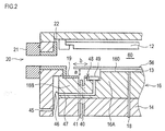
- FIG. 2 is an enlarged view of the outer periphery of the susceptor 16 when viewed from the side of the film forming chamber parallel to the gas flow direction
- FIG. 3 is an enlarged plan view showing a part of the periphery of the susceptor.
- the susceptor 16 is supported by the stage 14 and has a susceptor main body 16A having a holding surface 160 for holding the substrate 13 on the upper surface, and a susceptor peripheral portion 16B having a height lower than the holding surface 160 and located around the susceptor body 16A. is doing.
- the holding surface 160 has a shape that matches the size of the substrate 13.
- the mask 56 is installed on the susceptor 16 and has a size surrounding the substrate 13.
- substrate 13 is not specifically limited as this invention, In this embodiment, the magnitude
- the susceptor peripheral edge portion 16B has an inert gas supply port 48 formed on the upper surface close to the holding surface 160.
- the susceptor peripheral edge portion 16B is formed in a concave groove shape so as to surround the susceptor body 16A. Further, a ring plate-shaped shower plate 49 is installed in the concave groove so as to have a small gap between the bottom surface of the groove and the inner and outer peripheral surfaces of the groove.
- the shower plate 49 can secure a gap with the groove bottom by forming a discontinuous protrusion on the lower surface, for example, and can be formed with a width narrower than the inner and outer peripheral widths of the groove, so A small gap can be formed between the peripheral surface.
- the blow holes 49A having a predetermined diameter may be formed in the shower plate at a predetermined interval (for example, 100 mm pitch).
- the shower plate 49 preferably covers the periphery of the substrate 13.
- the inert gas supply port 48 has a shower head structure. The shower head structure makes it possible to blow out the inert gas evenly around the susceptor body 16A.
- the susceptor peripheral part 16B has an inert gas supply path 47 communicating with the inert gas supply port 48 inside, and the end of the inert gas supply path 47 reaches the outer peripheral wall of the susceptor peripheral part 16B. Yes.
- One or a plurality of inert gas supply paths 47 may be formed.
- the inert gas supply path 47 may be formed with a diameter of 3 mm.
- An inert gas supply tube 46 disposed on the outer peripheral side of the susceptor 16 is connected to the inert gas supply path 47, and the other end side of the inert gas supply tube 46 is an inert gas provided in the film forming container 11.
- the gas vent 45 is connected.
- An inert gas supply unit (not shown) is connected to the inert gas vent 45.
- the inert gas supply tube 46 can be composed of, for example, a stainless steel tube or a bellows flexible tube. When the substrate 13 is carried into or out of the film formation container 11, the stage 14 moves up and down, but the inert gas supply tube 46 needs to follow its up and down operation.
- the inert gas supply tube 46 also constitutes a part of the inert gas supply path.
- a mask pin hole 40 penetrating the stage 14 and the susceptor peripheral edge portion 16B is formed on the outer peripheral side of the inert gas supply port 48, and the mask pin hole 40 can be operated vertically.
- a mask pin 41 that can move the mask 56 up and down is inserted.
- the exposed surface of the upper surface except the inert gas supply port 48 and the mask pin hole 40 is covered with the susceptor deposition preventing plate 19. It is desirable that the upper surface height of the susceptor deposition preventing plate 19 be flush with the upper surface height of the shower plate 49.
- the distance a formed between the lower surface of the mask 56 and the upper surface of the susceptor deposition preventing plate 19 is preferably 0.1 mm or more and 10 mm or less, and more preferably 1 mm. As the distance a is smaller, it is possible to suppress the amount of the raw material gas and the reactive gas that enter the gap, and the necessary inert gas supply amount is also reduced.
- the mask is preferably an insulator, but may be a metal such as stainless steel. However, when the mask is made of metal, there is a possibility that discharge occurs in the gap. In that case, the pressure of the gap is adjusted using Baschen's law so that the product of the distance a and the pressure of the gap does not satisfy the discharge condition.
- the distance b between the outer peripheral edge of the mask 56 and the susceptor deposition preventing plate 19, that is, the distance from the outer peripheral side end of the inert gas supply port 48 is preferably 1 mm or more and 200 mm or less, Furthermore, it is preferable that it is 20 mm. This is because if the distance b is small, even if an inert gas is supplied, the shower plate 49 may enter due to the diffusion of the source gas and the reaction gas. If the value is too large, the size of the mask and the vacuum container also increases, which is not preferable.
- the inert gas supplied from the inert gas supply unit passes through the shower plate 49 through the inert gas vent 45, the inert gas supply tube 46, the inert gas supply path 47, and the inert gas supply port 48. Then, the air is blown out through the gap between the shower plate 49 and the inert gas supply port 48 or the blowout hole 49A.
- the inert gas passes through a gap formed by the mask 56 and the susceptor deposition prevention plate 19, is exhausted to the outer peripheral side of the susceptor 16, and is exhausted through the exhaust unit 30.
- the susceptor adhesion prevention board 19 on the susceptor peripheral part 16B only the susceptor peripheral part 16B may be sufficient. At this time, the distance between the upper surface of the susceptor peripheral edge portion 16B and the lower surface of the mask 56 is a, and the distance from the outer peripheral end of the mask 56 to the outer peripheral end side of the shower plate 49 is b.
- the inert gas is discharged from the inert gas supply port 48 after being heated to a temperature within ⁇ 10% of the stage temperature.
- a temperature within ⁇ 10% of the stage temperature For example, in the case where the stage is heated to 100 ° C., if an inert gas at room temperature is supplied, the outer periphery of the susceptor 16 is cooled, so that the temperature distribution of the substrate 13 is also lowered, and the film thickness uniformity and film quality uniformity are lowered. Therefore, in order to keep the temperature of the susceptor 16 constant, it is preferable to supply an inert gas of 90 to 110 ° C., for example.
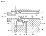
- FIG. 4 shows a susceptor configuration in which the installation position of the inert gas supply port of FIG. 2 is optimized.
- the mask pin hole 40 cannot completely seal the film formation space 60 and the transfer chamber space 61, if there is a pressure difference between them, the gas will flow to either one.
- the stage 14, the susceptor 16 and the transfer chamber space 61 are usually difficult to perform maintenance. Therefore, if particles are generated in these portions, it becomes difficult to remove the particles.
- the transfer chamber space 61 is positive pressure and the film formation space 60 is negative pressure
- the particles ride on the gas flow and are discharged into the film formation space 60, Since particles adhere, it is not preferable. Therefore, it is preferable that the film formation space 60 has a positive pressure and the transfer chamber space 61 has a negative pressure.
- the inert gas supplied from the inert gas supply port 48 is sucked into the mask pin hole 40, and at the same time, the raw material Gases and reactive gases may be inhaled. Even at the same pressure, there is a possibility that the source gas and the reaction gas diffuse to the mask pin hole by diffusion. Since the sucked source gas and reaction gas react, particles are generated in the mask pin hole. Therefore, the inert gas supply port is preferably provided on the outer peripheral side of the mask pin hole 40 as shown in FIG.
- FIG. 4 is an enlarged view of the outer periphery of the susceptor 16 when viewed from the side of the film forming chamber parallel to the gas flow direction
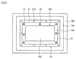
- FIG. 5 is an enlarged plan view showing a part of the periphery of the susceptor.
- the susceptor 16 is supported by the stage 14 and has a holding surface 160 that holds the substrate 13.
- the susceptor body 16 ⁇ / b> A is positioned around the periphery of the susceptor and has a lower height than the holding surface 160. Part 16B.
- the holding surface 160 has a shape that matches the size of the substrate 13.
- the mask 56 is installed on the susceptor 16 and has a size surrounding the substrate 13. The size exceeding the substrate 13 is also set to 50 mm or less as in the first embodiment.
- the susceptor peripheral edge portion 16B has a plurality of mask pin holes 40 penetrating the stage 14 and the susceptor peripheral edge portion 16B on the upper surface at a position close to the holding surface 160, and can be operated up and down in the mask pin hole 40.
- a mask pin 41 for moving the mask 56 up and down is inserted.
- an inert gas supply port 50 is formed in a recessed groove shape so as to surround the susceptor body 16A, and the bottom surface of the groove is formed in the recessed groove.
- the shower plate 51 is installed so as to have a small gap with the inner and outer peripheral surfaces.
- the shower plate 51 can secure a gap from the groove bottom by forming a discontinuous protrusion on the lower surface, for example. Further, the shower plate 51 may be formed with, for example, blowing holes 51A having a predetermined diameter (for example, 1 mm to 3 mm diameter) at predetermined intervals (for example, a pitch of 10 to 200 mm).
- a predetermined diameter for example, 1 mm to 3 mm diameter
- predetermined intervals for example, a pitch of 10 to 200 mm.
- the shower plate 51 preferably covers the periphery of the substrate 13.
- the inert gas supply port 50 has a shower head structure.
- a shower may be prepared by providing a blow hole in the susceptor peripheral edge portion 16B, or a shower plate may be separately manufactured and attached to the susceptor peripheral edge portion 16B.
- the exposed surface of the upper surface except the mask pin hole 40 and the inert gas supply port 50 is covered with a susceptor deposition preventing plate 19A.
- the upper surface height of the susceptor deposition preventing plate 19A is preferably flush with the upper surface height of the shower plate 51.
- the susceptor peripheral part 16B has an inert gas supply path 47 communicating with the inert gas supply port 50 inside, and the end of the inert gas supply path 47 reaches the outer peripheral wall of the susceptor peripheral part 16B. Yes.
- One or a plurality of inert gas supply paths 47 may be formed.
- the inert gas supply path 47 may be formed with a diameter of 3 mm.
- An inert gas supply tube 46 disposed on the outer peripheral side of the susceptor 16 is connected to the inert gas supply path 47, and the other end side of the inert gas supply tube 46 is an inert gas provided in the film forming container 11.
- the gas vent 45 is connected.
- An inert gas supply unit (not shown) is connected to the inert gas vent 45.
- the inert gas supply tube 46 can be composed of, for example, a stainless steel tube or a bellows flexible tube.
- the distance a formed between the lower surface of the mask 56 and the upper surface of the susceptor protection plate 19A is preferably 0.1 mm or more and 10 mm or less, and more preferably 1 mm. As the distance a is smaller, it is possible to suppress the amount of the raw material gas and the reactive gas that enter the gap, and the necessary inert gas supply amount is also reduced.
- the mask is preferably an insulator, but may be a metal such as stainless steel. However, when the mask is made of metal, there is a possibility that discharge occurs in the gap. In that case, the pressure of the gap is adjusted using Baschen's law so that the product of the distance a and the pressure of the gap does not satisfy the discharge condition.
- the distance b between the outer peripheral edge of the mask 56 and the susceptor deposition preventing plate 19A, that is, the distance from the outer peripheral edge of the inert gas supply port 50 is preferably 1 mm or more and 200 mm or less. Furthermore, it is preferable that it is 20 mm. This is because if the distance b is small, even if an inert gas is supplied, the shower plate 51 may enter due to the diffusion of the source gas and the reaction gas. If the value is too large, the size of the mask and the vacuum container also increases, which is not preferable. However, in this embodiment, the inert gas is blown out on the outer peripheral side of the mask pin 40, and the effect of suppressing the diffusion of the source gas and the reaction gas is great.
- the inert gas supplied from the inert gas supply unit passes through the shower plate 51 through the inert gas vent 45, the inert gas supply tube 46, the inert gas supply path 47, and the inert gas supply port 50. Then, the air is blown out through a gap with the inert gas supply port 50 and the blowout hole 51A, and is supplied to the exhaust unit 30 through a gap formed by the mask 56 and the susceptor deposition preventing plate 19A.
- the susceptor deposition preventing plate 19A may be provided. At this time, the distance between the upper surface of the susceptor peripheral edge portion 16B and the lower surface of the mask 56 is a, and the distance from the outer peripheral end of the mask 56 to the outer peripheral end side of the shower plate 51 is b.
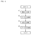
- FIG. 6 is a flowchart showing an example of the atomic layer deposition method of the present embodiment.
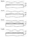
- 7A to 7D are diagrams showing a process of forming a thin film on the substrate S.
- the source gas supply unit supplies source gas into the film formation container 11 (step s1). Specifically, the source gas is supplied to the gas introduction unit 20. The source gas is supplied into the film forming container 11. The source gas is supplied into the film forming container 11 for 0.1 seconds, for example. As shown in FIG. 7A, in step s1, the source gas 110 is supplied to the inside of the film forming container 11, and the source gas 110 is adsorbed on the substrate S, so that the adsorption layer 102 is formed.
- step s 1 an inert gas is supplied to the inner surface of the injector 21 and the outer surface of the injector deposition preventing material 22. Further, the exhaust unit 30 also supplies an inert gas to the exhaust gas-proofing material 31 and the exhaust pipe connection unit 32. Further, the inert gas is supplied also to the susceptor peripheral edge portion 16B. In this embodiment, the inert gas is always supplied including not only step s1 but also steps s2 to s4 described later.
- the gap between the film forming container 11 and the injector deposition preventing material 22, the gap between the film forming container 11 and the exhaust deposition preventing material 31, and The source gas can be prevented from entering the gap between the mask 56 and the susceptor 16.
- the supply of the source gas is stopped, and the purge gas is supplied at the gas introduction part (step s2).
- the purge gas is supplied into the film forming container 11.
- the source gas is discharged from the exhaust unit 30 to the outside of the film forming container 11.
- the purge gas is supplied into the film forming container 11 for 0.1 seconds, for example.
- the exhaust unit 30 exhausts the source gas 110 and the purge gas 112 inside the film formation container 11.
- the exhaust unit 30 exhausts the source gas 110 and the purge gas 112 inside the film formation container 11 for 2 seconds, for example.
- the purge gas 112 is supplied into the film forming container 11 and the source gas 110 not adsorbed on the substrate S is purged from the film forming container 11 in step s2.
- a reactive gas is supplied into the film formation container 11 (step s3).
- the reaction gas is supplied through the gas introduction unit 20.
- the reaction gas is supplied to the inside of the film forming container 11 through the passage of the gas introduction unit 20.
- the reaction gas is supplied into the film formation container 11 for 1 second, for example.
- the reaction gas 114 is supplied into the film formation container 11 in step s3.
- step s3 an inert gas is supplied from the inner surface of the injector 21, the outer surface of the injector deposition material 22, the exhaust portion 30, and the susceptor peripheral portion 16B. Therefore, in step S3, when the reaction gas is supplied to the inside of the film forming container 11, the gap between the film forming container 11 and the injector deposition preventing material 22, the gap between the film forming container 11 and the exhaust deposition preventing material 31, and The reaction gas can be prevented from entering the gap between the mask 56 and the susceptor 16.
- step s4 the supply of the reaction gas is stopped, and the purge gas is supplied to the gas introduction unit 20 (step s4).
- the purge gas is supplied into the film forming container 11.
- the purge gas is discharged from the exhaust unit 30 to the outside of the film formation container 11.
- the purge gas is supplied into the film forming container 11 for 0.1 seconds, for example.
- the exhaust unit 30 exhausts the reaction gas 114 and the purge gas 112 inside the film formation container 11.
- step s4 the purge gas 112 is supplied into the film formation container 11 and the reaction gas 114 is purged from the film formation container 11.
- the thin film layer 104 for one atomic layer is formed on the substrate S by the steps s1 to s4 described above. Thereafter, the thin film layer 104 having a desired film thickness can be formed by repeating steps s1 to s4 a predetermined number of times.
- the inert gas flows on the inner surface of the injector 21 and the outer surface of the injector deposition material 22, the source gas and the reactive gas are in the gap between the film forming container 11 and the injector 21. Intrusion can be suppressed. Therefore, it is possible to suppress the thin film from adhering to the gap between the film forming container 11 and the injector 21. Similarly, the exhaust portion 30 is also prevented from attaching a thin film. Further, since the inert gas flows out at the susceptor peripheral edge portion 16B, deposition on the mask bottom surface, the substrate side surface, the substrate bottom surface, the susceptor and the like is prevented.
- an alumina film formed using TMA as a source gas and O 3 as a reaction gas can be subjected to gas etching using BCl 3 gas.
- gas-etch the alumina film with BCl 3 gas it is necessary to heat it to a high temperature of about 500 ° C., for example.
- the stage 14 is provided with a heater (not shown), and the inner wall of the film forming container 11 located in the vicinity of the heater can be heated to a high temperature of about 500 ° C. by the heater. Therefore, the thin film adhering to the inner wall of the film forming container 11 located near the heater can be removed by gas etching.
- the thin film adhering to the inner wall and the susceptor of the film forming container 11 it is possible to suppress the thin film from adhering to the inner wall and the susceptor of the film forming container 11, and the thin film adhering to the inner wall and the susceptor can be removed by gas etching.
- the frequency of cleaning by wet etching can be reduced.
- TMA trimethylaluminum
- Al source oxygen plasma and nitrogen plasma
- the film formation was performed in the sequence shown in FIG.
- the pressure inside the film formation container was 100 Pa, and 500 sccm of nitrogen was supplied from the inert gas supply unit, and was always supplied during the film formation sequence.
- After film formation of 20 ⁇ m when the amount of film deposited on the lower surface of the mask 56 and the upper surface of the susceptor deposition preventing plate 19A is visually observed, no interference film due to the thin film is observed, and it is confirmed that the film amount is 50 nm or less. It was done. Therefore, it has been confirmed that the cleaning frequency of the mask and the susceptor can be reduced while the structure can easily cope with the substrate size change and the process condition change.
Landscapes
- Chemical & Material Sciences (AREA)
- Engineering & Computer Science (AREA)
- Mechanical Engineering (AREA)
- Chemical Kinetics & Catalysis (AREA)
- Materials Engineering (AREA)
- Metallurgy (AREA)
- Organic Chemistry (AREA)
- General Chemical & Material Sciences (AREA)
- Physics & Mathematics (AREA)
- Plasma & Fusion (AREA)
- Inorganic Chemistry (AREA)
- Electromagnetism (AREA)
- Chemical Vapour Deposition (AREA)
Abstract
基板上に薄膜を形成する原子層成長装置であって、成膜容器と、成膜容器内に設置されたステージと、ステージ上で基板を保持するサセプタと、基板上に配置され、基板を囲む大きさのマスクと、マスクを支持して上下に可動可能なマスクピンと、ステージおよびサセプタを上下に貫通して、マスクピンが上下動可能に挿通されるマスクピン穴を備え、サセプタは、基板の保持面を有するサセプタ本体と、サセプタ本体の周囲に位置して保持面よりも低い高さのサセプタ周縁部とを有し、マスクピン穴は、サセプタ周縁部に開口し、サセプタ周縁部には、マスクの囲み領域内で、保持面の周囲にガスを上方側に排出する不活性ガス供給口が設けられ、不活性ガス供給口に不活性ガスを供給する不活性ガス供給路が接続されている。
Description
本発明は、基板上に薄膜を形成する原子層成長装置に関する。
原子層成長法は、形成しようとする薄膜を構成する元素のガスを基板上に交互に供給し、基板上に原子層単位で薄膜を形成するもので、薄膜を均一に形成する技術として知られている。原子層成長法は、一般的なCVD(Chemical Vapor Deposition)法と比較して、段差被覆性や膜厚制御性に優れている。
従来のスパッタ成膜装置においては、特許文献1のようなマスクを利用することが可能である。スパッタ成膜は膜の段差被覆性が低いため、マスク裏面への成膜量は小さいため、パーティクル発生量は小さく、メンテナンス周期も長い。しかし、原子層成長成膜においては、膜の段差被覆性が高いため、マスク裏面への着膜量は多い。微細な隙間に侵入したガスは、厚膜及び粉となり、パーティクルの要因となる。特にマスクの表面粗さは、マスクの平坦性を維持するために大きくできないため、マスク交換頻度が増大する。
そこで、マスクを利用した原子層成長成膜においては、サセプタ周辺からの不活性ガスパージが有効となる。特許文献2では、ステージにガス供給口を設け、サセプタの裏面から不活性ガスを供給している。
しかし、特許文献2に示された装置に従って、ステージ本体にガス供給口を設けると、ステージの設計及び作製が煩雑となる。よって、基板サイズが変更される場合は、ステージ自体の構成の変更が必要となるため汎用性が低いという問題がある。
本発明は、上記事情を背景としてなされたものであり、マスク裏面への着膜を抑制し、かつ、基板サイズの変更に容易に対応することができる原子層成長装置を提供することを目的の一つとする。
本発明の原子層成長装置のうち、第1の形態は、
基板上に薄膜を形成する原子層成長装置であって、
成膜容器と、
前記成膜容器内に設置されたステージと、
前記ステージ上で前記基板を保持するサセプタと、
前記基板上に配置され、前記基板を囲む大きさのマスクと、
前記マスクを支持して上下に可動可能なマスクピンと、
前記ステージおよび前記サセプタを上下に貫通して、前記マスクピンが上下動可能に挿通されるマスクピン穴と、を備え、
前記サセプタは、前記基板の保持面を有するサセプタ本体と、前記サセプタ本体の周囲に位置して前記保持面よりも低い高さのサセプタ周縁部とを有し、
前記マスクピン穴は、前記サセプタ周縁部に開口し、
前記サセプタ周縁部には、前記マスクの囲み領域内で、前記保持面の周囲にガスを上方側に排出する不活性ガス供給口が設けられ、前記不活性ガス供給口に不活性ガスを供給する不活性ガス供給路が接続されていることを特徴とする。
基板上に薄膜を形成する原子層成長装置であって、
成膜容器と、
前記成膜容器内に設置されたステージと、
前記ステージ上で前記基板を保持するサセプタと、
前記基板上に配置され、前記基板を囲む大きさのマスクと、
前記マスクを支持して上下に可動可能なマスクピンと、
前記ステージおよび前記サセプタを上下に貫通して、前記マスクピンが上下動可能に挿通されるマスクピン穴と、を備え、
前記サセプタは、前記基板の保持面を有するサセプタ本体と、前記サセプタ本体の周囲に位置して前記保持面よりも低い高さのサセプタ周縁部とを有し、
前記マスクピン穴は、前記サセプタ周縁部に開口し、
前記サセプタ周縁部には、前記マスクの囲み領域内で、前記保持面の周囲にガスを上方側に排出する不活性ガス供給口が設けられ、前記不活性ガス供給口に不活性ガスを供給する不活性ガス供給路が接続されていることを特徴とする。
第2の形態の原子層成長装置の本発明は、前記形態の本発明において、前記サセプタ本体を基準にして、前記マスクピン穴よりも外側に、前記不活性ガス供給口が設けられていることを特徴とする。
第3の形態の原子層成長装置の本発明は、前記形態の本発明において、前記不活性ガス供給口が、前記保持面の周囲で全周に沿って複数個または全周に亘って連続して形成されていることを特徴とする。
第4の形態の原子層成長装置の本発明は、前記形態の本発明において、前記不活性ガス供給口が前記不活性ガス供給路に対しシャワーヘッド構造を有することを特徴とする。
第5の形態の原子層成長装置の本発明は、前記形態の本発明において、前記マスクと前記サセプタ周縁部との間に形成される隙間が0.1mm以上、10mm以下であることを特徴とする。
第6の形態の原子層成長装置の本発明は、前記形態の本発明において、前記マスク周縁端と前記不活性ガス供給口の近接側との距離が1mm以上、200mm以下であることを特徴とする。
第7の形態の原子層成長装置の本発明は、前記形態の本発明において、前記サセプタ周縁部上面に、防着材が設置されていることを特徴とする。
第8の形態の原子層成長装置の本発明は、前記形態の本発明において、前記不活性ガスは、ステージ面温度と±10%以内の温度で前記不活性ガス供給口から排出されることを特徴とする。
本発明によれば、マスク裏面への着膜を抑制し、基板サイズ変更に容易に対応できるため、マスク及びサセプタのクリーニング頻度を低減することが可能となり、且つ様々な基板サイズ、プロセス条件に対応可能となる。
まず、図1を参照して、本実施形態の原子層成長装置の構成を説明する。図1は、本実施形態の原子層成長装置の一例を示す概略構成図である。
本実施形態の原子層成長装置10は、原料ガスと反応ガスとを交互に供給し、基板13上に原子層単位で薄膜を形成する。その際、反応活性を高めるため、基板13を加熱させることができる。本実施形態では原料ガスとしてTMA(Tri-Methyl-Aluminum)を用い、その際、反応活性を高めるため、プラズマを発生させる。本実施形態では、プラズマの発生に平行平板電極を用いるが、この方式に限定されない。
成膜容器11は原料ガス、反応ガス、パージガスを導入するガス導入部20と排気部30と、ステージ14と、平板電極12と、高周波電源15と、サセプタ16と、基板搬入口17と、基板13上に配置するマスク56と、を備える。ガス導入部20は、成膜容器11外側から設けられたインジェクタ21と、成膜容器11内側から設けられたインジェクタ防着材22を有し、排気部30は、成膜容器11内側から設けられた排気防着材31と成膜容器11外側から設けられた排気配管接続部32とを有している。
本実施形態の原子層成長装置10は、原料ガスと反応ガスとを交互に供給し、基板13上に原子層単位で薄膜を形成する。その際、反応活性を高めるため、基板13を加熱させることができる。本実施形態では原料ガスとしてTMA(Tri-Methyl-Aluminum)を用い、その際、反応活性を高めるため、プラズマを発生させる。本実施形態では、プラズマの発生に平行平板電極を用いるが、この方式に限定されない。
成膜容器11は原料ガス、反応ガス、パージガスを導入するガス導入部20と排気部30と、ステージ14と、平板電極12と、高周波電源15と、サセプタ16と、基板搬入口17と、基板13上に配置するマスク56と、を備える。ガス導入部20は、成膜容器11外側から設けられたインジェクタ21と、成膜容器11内側から設けられたインジェクタ防着材22を有し、排気部30は、成膜容器11内側から設けられた排気防着材31と成膜容器11外側から設けられた排気配管接続部32とを有している。
ステージ14はヒータ(図示しない)を備え、基板13の温度を調整することができる。例えば、プラズマ原子層成長成膜の場合、基板13を50~200℃に加熱する。
平板電極12は高周波電源15と接続されている。高周波電源15が所定の周波数の高周波電流を供給することにより、平板電極12とステージ14との間でプラズマが生成される。
基板13は、ステージ14の下方からリフトピン18によって支持される。リフトピン18は、ステージ14の昇降によって、基板13の受け渡しを搬送室空間61にて可能とする。
原料ガス、反応ガス、パージガスを導入するガス導入部20は、原料ガス、反応ガス、パージガスを成膜容器11内に供給する。排気部30は、原料ガス、反応ガス、パージガスを成膜容器11から外部に排気する。
図1は、原子層成長装置の基本構造を示しており、以下で説明する一部の構成は省略している。
平板電極12は高周波電源15と接続されている。高周波電源15が所定の周波数の高周波電流を供給することにより、平板電極12とステージ14との間でプラズマが生成される。
基板13は、ステージ14の下方からリフトピン18によって支持される。リフトピン18は、ステージ14の昇降によって、基板13の受け渡しを搬送室空間61にて可能とする。
原料ガス、反応ガス、パージガスを導入するガス導入部20は、原料ガス、反応ガス、パージガスを成膜容器11内に供給する。排気部30は、原料ガス、反応ガス、パージガスを成膜容器11から外部に排気する。
図1は、原子層成長装置の基本構造を示しており、以下で説明する一部の構成は省略している。
(実施形態1)
図2は、ガス流れ方向に平行な成膜室側面から見た場合のサセプタ16外周の拡大図であり、図3は、サセプタ周辺の一部を示す拡大平面図である。
サセプタ16は、ステージ14に支持され、基板13を保持する保持面160を上面に有するサセプタ本体16Aと、その周囲に位置して保持面160よりも低い高さ面のサセプタ周縁部16Bとを有している。保持面160は、基板13の大きさに合わせた形状を有している。
図2は、ガス流れ方向に平行な成膜室側面から見た場合のサセプタ16外周の拡大図であり、図3は、サセプタ周辺の一部を示す拡大平面図である。
サセプタ16は、ステージ14に支持され、基板13を保持する保持面160を上面に有するサセプタ本体16Aと、その周囲に位置して保持面160よりも低い高さ面のサセプタ周縁部16Bとを有している。保持面160は、基板13の大きさに合わせた形状を有している。
マスク56は、サセプタ16上に設置され、基板13を囲む大きさを有している。基板13を超える大きさは、本発明としては特に限定されるものではないが、この実施形態では、基板13を超えている大きさを50mm以下とする。
サセプタ周縁部16Bは、保持面160に近い側の上面に、不活性ガス供給口48が形成されており、この実施形態では、凹溝形状でサセプタ本体16Aを囲むように形成されている。さらに、凹溝内には、溝の底面と溝の内外周面との間で小隙間を有するように、リング板状のシャワープレート49が設置されている。
サセプタ周縁部16Bは、保持面160に近い側の上面に、不活性ガス供給口48が形成されており、この実施形態では、凹溝形状でサセプタ本体16Aを囲むように形成されている。さらに、凹溝内には、溝の底面と溝の内外周面との間で小隙間を有するように、リング板状のシャワープレート49が設置されている。
シャワープレート49は、例えば下面に不連続の突部を形成することで、溝底面と隙間を確保することができ、また、溝の内外周幅よりも狭い幅で形成することで、溝の内外周面との間で小隙間を形成することができる。また、シャワープレートには、例えば、所定径(例えば1mm径)の吹き出し穴49Aを所定間隔(例えば100mmピッチ)で形成するようにしてもよい。
なお、シャワープレート49は、基板13の周囲を覆っていることが好ましい。
上記シャワープレート49により不活性ガス供給口48は、シャワーヘッド構造を有する。シャワーヘッド構造により、不活性ガスをサセプタ本体16Aの周りで均等に吹き出すことが可能になる。
なお、シャワープレート49は、基板13の周囲を覆っていることが好ましい。
上記シャワープレート49により不活性ガス供給口48は、シャワーヘッド構造を有する。シャワーヘッド構造により、不活性ガスをサセプタ本体16Aの周りで均等に吹き出すことが可能になる。
サセプタ周縁部16Bは、内部に前記不活性ガス供給口48に連通する不活性ガス供給路47を有しており、該不活性ガス供給路47の終端はサセプタ周縁部16Bの外周壁に達している。不活性ガス供給路47は、一つまたは複数を形成してもよく、例えば、3mm径で形成することができる。
不活性ガス供給路47には、サセプタ16の外周側に配置した不活性ガス供給チューブ46が接続されており、不活性ガス供給チューブ46の他端側は、成膜容器11に設けた不活性ガス通気口45に接続されている。不活性ガス通気口45には、図示しない不活性ガス供給部が接続されている。
不活性ガス供給チューブ46は、例えば、ステンレス製チューブ、ベローズフレキシブルチューブなどで構成することができる。基板13を成膜容器11内に搬入または搬出する際にはステージ14が上下するが、不活性ガス供給チューブ46はその上下稼働に追従することが必要となる。不活性ガス供給チューブ46も不活性ガス供給路の一部を構成するものである。
不活性ガス供給路47には、サセプタ16の外周側に配置した不活性ガス供給チューブ46が接続されており、不活性ガス供給チューブ46の他端側は、成膜容器11に設けた不活性ガス通気口45に接続されている。不活性ガス通気口45には、図示しない不活性ガス供給部が接続されている。
不活性ガス供給チューブ46は、例えば、ステンレス製チューブ、ベローズフレキシブルチューブなどで構成することができる。基板13を成膜容器11内に搬入または搬出する際にはステージ14が上下するが、不活性ガス供給チューブ46はその上下稼働に追従することが必要となる。不活性ガス供給チューブ46も不活性ガス供給路の一部を構成するものである。
また、サセプタ周縁部16Bでは、不活性ガス供給口48の外周側に、ステージ14およびサセプタ周縁部16Bを貫通するマスクピン穴40が形成されており、マスクピン穴40内に、上下に稼働可能で、マスク56を上下に移動することができるマスクピン41が挿入されている。
また、サセプタ周縁部16Bでは、不活性ガス供給口48およびマスクピン穴40を除いて、上面の露出面に、サセプタ防着板19が被覆されている。サセプタ防着板19の上面高さは、シャワープレート49の上面高さと面一にするのが望ましい。
また、サセプタ周縁部16Bでは、不活性ガス供給口48およびマスクピン穴40を除いて、上面の露出面に、サセプタ防着板19が被覆されている。サセプタ防着板19の上面高さは、シャワープレート49の上面高さと面一にするのが望ましい。
ここで、マスク56下面とサセプタ防着板19上面とで形成される距離aは、0.1mm以上、10mm以下であることが好ましく、さらには1mmであることが好ましい。距離aが小さいほど、隙間へ侵入する原料ガス及び反応ガス量を抑制することが可能となり、必要とする不活性ガス供給量も低減する。マスクは絶縁体であることが好ましいが、ステンレス等の金属でもよい。ただし、マスクが金属の場合は、前記隙間で放電を生じる可能性がある。その場合は、バッシェンの法則を利用し、前記距離aと前記隙間の圧力との積が放電条件を満たさないよう、前記隙間の圧力調整を行う。
また、マスク56の外周縁端とサセプタ防着板19との重なりの距離b、すなわち、不活性ガス供給口48の外周側端部との距離は、1mm以上、200mm以下であることが好ましく、さらには20mmであることが好ましい。距離bが小さいと、不活性ガスが供給されていても、原料ガス及び反応ガスの拡散によりシャワープレート49まで侵入する可能性があるためである。値が大きすぎると、マスク及び真空容器サイズも大きくなるため、好ましくない。
不活性ガス供給部から供給された不活性ガスは、不活性ガス通気口45、不活性ガス供給チューブ46、不活性ガス供給路47、不活性ガス供給口48を通り、シャワープレート49を経由して、シャワープレート49と不活性ガス供給口48との隙間や吹き出し穴49Aを通して吹き出される。不活性ガスは、マスク56とサセプタ防着板19により形成される隙間を通り、サセプタ16の外周側に排気され、排気部30を通って排気される。
また、サセプタ防着板19をサセプタ周縁部16B上に設けることが好ましいが、サセプタ周縁部16Bのみでもよい。このときは、サセプタ周縁部16B上面とマスク56下面との距離がaとなり、マスク56外周端からシャワープレート49の外周端側までの距離がbとなる。
また、サセプタ防着板19をサセプタ周縁部16B上に設けることが好ましいが、サセプタ周縁部16Bのみでもよい。このときは、サセプタ周縁部16B上面とマスク56下面との距離がaとなり、マスク56外周端からシャワープレート49の外周端側までの距離がbとなる。
また、不活性ガスは、ステージ温度と±10%以内の温度まで加熱されたあとに前記不活性ガス供給口48から放出されることが好ましい。例えば、ステージを100℃に加熱する場合、常温の不活性ガスを供給すると、サセプタ16外周が冷却されるため、基板13の温度分布も低下し、膜厚均一性および膜質均一性が低下する。よって、サセプタ16の温度を一定に保つため、例えば90~110℃の不活性ガスを供給することが好ましい。
(実施形態2)
図4は、図2の不活性ガス供給口の設置位置を最適化したサセプタ構成である。
マスクピン穴40が、成膜空間60と搬送室空間61を完全にシールすることができない場合、両者に圧力差があると、ガスはどちらか一方へ流れることになる。
ステージ14、サセプタ16および搬送室空間61は、通常、メンテナンスを実施するのが困難である。よって、これら部分にパーティクルを生じてしまうと、パーティクルの除去は困難となる。例えば、マスクピン穴40にパーティクルが存在する状態で、搬送室空間61が正圧、成膜空間60が負圧であれば、パーティクルがガス流に乗って成膜空間60に放出され、基板13にパーティクルが付着するため好ましくない。よって、成膜空間60が正圧、搬送室空間61が負圧であることが好ましい。
図4は、図2の不活性ガス供給口の設置位置を最適化したサセプタ構成である。
マスクピン穴40が、成膜空間60と搬送室空間61を完全にシールすることができない場合、両者に圧力差があると、ガスはどちらか一方へ流れることになる。
ステージ14、サセプタ16および搬送室空間61は、通常、メンテナンスを実施するのが困難である。よって、これら部分にパーティクルを生じてしまうと、パーティクルの除去は困難となる。例えば、マスクピン穴40にパーティクルが存在する状態で、搬送室空間61が正圧、成膜空間60が負圧であれば、パーティクルがガス流に乗って成膜空間60に放出され、基板13にパーティクルが付着するため好ましくない。よって、成膜空間60が正圧、搬送室空間61が負圧であることが好ましい。
しかし、図2で示したサセプタ構造の場合、成膜空間60と搬送室空間61の圧力差次第では、不活性ガス供給口48から供給された不活性ガスがマスクピン穴40へ吸い込まれ、同時に原料ガスおよび反応ガスを吸い込む可能性がある。同圧であっても、拡散によりマスクピン穴まで原料ガス及び反応ガスが拡散する可能性が有る。吸い込まれた原料ガス及び反応ガスは反応するため、マスクピン穴でパーティクルが発生する。よって、不活性ガス供給口は図4のようにマスクピン穴40よりも外周側へ設けることが好ましい。
上記に沿った原子層成長装置の構成を図4に基づいて説明する。なお、原子層成長装置の基本構成は図1に示すように、前記実施形態1と同様であり、その記載を省略または簡略にする。
図4は、ガス流れ方向に平行な成膜室側面から見た場合のサセプタ16外周の拡大図であり、図5は、サセプタ周辺の一部を示す拡大平面図である。
サセプタ16は、前記実施形態1と同様に、ステージ14に支持され、基板13を保持する保持面160を有するサセプタ本体16Aと、その周囲に位置して保持面160よりも低い高さのサセプタ周縁部16Bとを有している。保持面160は、基板13の大きさに合わせた形状を有している。
マスク56は、サセプタ16上に設置され、基板13を囲む大きさを有している。基板13を超えている大きさも実施形態1と同様に50mm以下とする。
図4は、ガス流れ方向に平行な成膜室側面から見た場合のサセプタ16外周の拡大図であり、図5は、サセプタ周辺の一部を示す拡大平面図である。
サセプタ16は、前記実施形態1と同様に、ステージ14に支持され、基板13を保持する保持面160を有するサセプタ本体16Aと、その周囲に位置して保持面160よりも低い高さのサセプタ周縁部16Bとを有している。保持面160は、基板13の大きさに合わせた形状を有している。
マスク56は、サセプタ16上に設置され、基板13を囲む大きさを有している。基板13を超えている大きさも実施形態1と同様に50mm以下とする。
サセプタ周縁部16Bは、保持面160に近接した位置の上面に、ステージ14およびサセプタ周縁部16Bを貫通するマスクピン穴40が複数個形成されており、マスクピン穴40内に、上下に稼働可能で、マスク56を上下に移動するマスクピン41が挿入されている。
サセプタ本体16Aを基準にして、マスクピン穴40の外周側には、不活性ガス供給口50が、凹溝形状でサセプタ本体16Aを囲むように形成されており、該凹溝内に、溝の底面と内外周面と小隙間を有するように、シャワープレート51が設置されている。シャワープレート51は、例えば下面に不連続の突部を形成することで、溝底面と隙間を確保することができる。また、シャワープレート51には、例えば、所定径(例えば1mm~3mm径)の吹き出し穴51Aを所定間隔(例えば10~200mmピッチ)で形成するようにしてもよい。
サセプタ本体16Aを基準にして、マスクピン穴40の外周側には、不活性ガス供給口50が、凹溝形状でサセプタ本体16Aを囲むように形成されており、該凹溝内に、溝の底面と内外周面と小隙間を有するように、シャワープレート51が設置されている。シャワープレート51は、例えば下面に不連続の突部を形成することで、溝底面と隙間を確保することができる。また、シャワープレート51には、例えば、所定径(例えば1mm~3mm径)の吹き出し穴51Aを所定間隔(例えば10~200mmピッチ)で形成するようにしてもよい。
なお、シャワープレート51は、基板13の周囲を覆っていることが好ましい。
上記シャワープレート51により不活性ガス供給口50は、シャワーヘッド構造を有する。
また、シャワーヘッド構造では、サセプタ周縁部16Bに吹き出し穴を設けてシャワーを作製してもよく、シャワープレートを個別に作製し、サセプタ周縁部16Bに取り付けてもよい。
なお、サセプタ周縁部16Bでは、マスクピン穴40および不活性ガス供給口50を除いて、上面の露出面にサセプタ防着板19Aが被覆されている。サセプタ防着板19Aの上面高さは、シャワープレート51の上面高さと面一になっているのが望ましい。
上記シャワープレート51により不活性ガス供給口50は、シャワーヘッド構造を有する。
また、シャワーヘッド構造では、サセプタ周縁部16Bに吹き出し穴を設けてシャワーを作製してもよく、シャワープレートを個別に作製し、サセプタ周縁部16Bに取り付けてもよい。
なお、サセプタ周縁部16Bでは、マスクピン穴40および不活性ガス供給口50を除いて、上面の露出面にサセプタ防着板19Aが被覆されている。サセプタ防着板19Aの上面高さは、シャワープレート51の上面高さと面一になっているのが望ましい。
サセプタ周縁部16Bは、内部に前記不活性ガス供給口50に連通する不活性ガス供給路47を有しており、該不活性ガス供給路47の終端はサセプタ周縁部16Bの外周壁に達している。不活性ガス供給路47は、一つまたは複数を形成してもよく、例えば、3mm径で形成することができる。
不活性ガス供給路47には、サセプタ16の外周側に配置した不活性ガス供給チューブ46が接続されており、不活性ガス供給チューブ46の他端側は、成膜容器11に設けた不活性ガス通気口45に接続されている。不活性ガス通気口45には、図示しない不活性ガス供給部が接続されている。不活性ガス供給チューブ46は、例えば、ステンレス製チューブ、ベローズフレキシブルチューブなどで構成することができる。
不活性ガス供給路47には、サセプタ16の外周側に配置した不活性ガス供給チューブ46が接続されており、不活性ガス供給チューブ46の他端側は、成膜容器11に設けた不活性ガス通気口45に接続されている。不活性ガス通気口45には、図示しない不活性ガス供給部が接続されている。不活性ガス供給チューブ46は、例えば、ステンレス製チューブ、ベローズフレキシブルチューブなどで構成することができる。
マスク56下面とサセプタ防着板19A上面とで形成される距離aは、0.1mm以上、10mm以下であることが好ましく、さらには1mmであることが好ましい。距離aが小さいほど、隙間へ侵入する原料ガス及び反応ガス量を抑制することが可能となり、必要とする不活性ガス供給量も低減する。マスクは絶縁体であることが好ましいが、ステンレス等の金属でもよい。ただし、マスクが金属の場合は、前記隙間で放電を生じる可能性がある。その場合は、バッシェンの法則を利用し、前記距離aと前記隙間の圧力との積が放電条件を満たさないよう、前記隙間の圧力調整を行う。
また、マスク56の外周縁端部とサセプタ防着板19Aとの重なりの距離b、すなわち、不活性ガス供給口50の外周端部との距離は、1mm以上、200mm以下であることが好ましく、さらには20mmであることが好ましい。距離bが小さいと、不活性ガスが供給されていても、原料ガス及び反応ガスの拡散によりシャワープレート51まで侵入する可能性があるためである。値が大きすぎると、マスク及び真空容器サイズも大きくなるため、好ましくない。
ただし、この実施形態では、マスクピン40の外周側で不活性ガスが吹き出しされており、原料ガスや反応ガスの拡散を抑止する作用が大きい。
ただし、この実施形態では、マスクピン40の外周側で不活性ガスが吹き出しされており、原料ガスや反応ガスの拡散を抑止する作用が大きい。
不活性ガス供給部から供給された不活性ガスは、不活性ガス通気口45、不活性ガス供給チューブ46、不活性ガス供給路47、不活性ガス供給口50を通り、シャワープレート51を経由して、不活性ガス供給口50との隙間や吹き出し穴51Aを通して吹き出され、マスク56とサセプタ防着板19Aにより形成される隙間を通り、排気部30へ供給される。
また、サセプタ防着板19Aをサセプタ周縁部16B上に設けることが好ましいが、サセプタ周縁部16Bのみでもよい。このときは、サセプタ周縁部16B上面とマスク56下面との距離がaとなり、マスク56外周端からシャワープレート51の外周端側までの距離がbとなる。
また、サセプタ防着板19Aをサセプタ周縁部16B上に設けることが好ましいが、サセプタ周縁部16Bのみでもよい。このときは、サセプタ周縁部16B上面とマスク56下面との距離がaとなり、マスク56外周端からシャワープレート51の外周端側までの距離がbとなる。
上記各実施形態で基板13のサイズが変更される場合は、サセプタ16のサイズを変更することで対応が可能であり、ステージ構成を変更する必要はない。また、プロセス条件変更の際、不活性ガス供給条件を伴うが、これも不活性ガス供給口、シャワープレートのみの変更でよい。
次に、上記原子層成長装置10における処理手順を説明する。
図6は、本実施形態の原子層堆積方法の一例を示すフローチャートである。図7A~Dは、基板Sの上に薄膜が形成される工程を示す図である。
図6は、本実施形態の原子層堆積方法の一例を示すフローチャートである。図7A~Dは、基板Sの上に薄膜が形成される工程を示す図である。
まず、原料ガス供給部が成膜容器11の内部に原料ガスを供給する(ステップs1)。具体的には、ガス導入部20に原料ガスを供給する。原料ガスは、成膜容器11の内部に供給される。原料ガスは、例えば、0.1秒間、成膜容器11の内部に供給する。図7Aに示されるように、ステップs1によって、成膜容器11の内部に原料ガス110が供給され、基板Sの上に原料ガス110が吸着して、吸着層102が形成される。
また、ステップs1において、インジェクタ21の内表面およびインジェクタ防着材22の外表面に不活性ガスを供給する。また、排出部30では、排気防着材31および排気配管接続部32にも不活性ガスを供給する。さらに、サセプタ周縁部16Bにおいても不活性ガスを供給する
本実施形態では、ステップs1のみでなく、後述するステップs2~s4も含めて、常に不活性ガスを供給する。そのため、ステップs1において、成膜容器11の内部に原料ガスを供給する際に、成膜容器11とインジェクタ防着材22との隙間および、成膜容器11と排気防着材31との隙間および、マスク56とサセプタ16との隙間に原料ガスが入り込むのを抑制することができる。
本実施形態では、ステップs1のみでなく、後述するステップs2~s4も含めて、常に不活性ガスを供給する。そのため、ステップs1において、成膜容器11の内部に原料ガスを供給する際に、成膜容器11とインジェクタ防着材22との隙間および、成膜容器11と排気防着材31との隙間および、マスク56とサセプタ16との隙間に原料ガスが入り込むのを抑制することができる。
次に、原料ガスの供給を停止し、ガス導入部でパージガスを供給する(ステップs2)。パージガスは、成膜容器11の内部に供給される。原料ガスは、排気部30から成膜容器11の外部に排出される。
パージガスは、例えば、0.1秒間、成膜容器11の内部に供給する。排気部30が成膜容器11の内部の原料ガス110やパージガス112を排気する。排気部30は、例えば、2秒間、成膜容器11の内部の原料ガス110やパージガス112を排気する。図7Bに示されるように、ステップs2によって、成膜容器11の内部にパージガス112が供給され、基板Sの上に吸着していない原料ガス110が成膜容器11からパージされる。
パージガスは、例えば、0.1秒間、成膜容器11の内部に供給する。排気部30が成膜容器11の内部の原料ガス110やパージガス112を排気する。排気部30は、例えば、2秒間、成膜容器11の内部の原料ガス110やパージガス112を排気する。図7Bに示されるように、ステップs2によって、成膜容器11の内部にパージガス112が供給され、基板Sの上に吸着していない原料ガス110が成膜容器11からパージされる。
次に、成膜容器11の内部に反応ガスを供給する(ステップs3)。具体的には、ガス導入部20を通して反応ガスを供給する。反応ガスは、ガス導入部20の通路を通って、成膜容器11の内部に供給される。反応ガスは、例えば、1秒間、成膜容器11の内部に供給される。図7Cに示されるように、ステップs3によって、成膜容器11の内部に反応ガス114が供給される。
また、ステップs3においても、インジェクタ21の内表面やインジェクタ防着材22の外表面や排気部30、サセプタ周縁部16Bで不活性ガスを供給する。そのため、ステップS3において、成膜容器11の内部に反応ガスを供給する際に、成膜容器11とインジェクタ防着材22との隙間および、成膜容器11と排気防着材31との隙間および、マスク56とサセプタ16との隙間に反応ガスが入り込むのを抑制することができる。
次に、反応ガスの供給を停止し、ガス導入部20にパージガスを供給する(ステップs4)。パージガスは、成膜容器11の内部に供給される。パージガスは、排気部30から成膜容器11の外部に排出される。パージガスは、例えば、0.1秒間、成膜容器11の内部に供給される。排気部30が、成膜容器11の内部の反応ガス114やパージガス112を排気する。図7Dに示されるように、ステップs4によって、成膜容器11の内部にパージガス112が供給され、反応ガス114が成膜容器11からパージされる。
以上説明したステップs1~s4により、基板Sの上に一原子層分の薄膜層104が形成される。以下、ステップs1~s4を所定回数繰り返すことにより、所望の膜厚の薄膜層104を形成することができる。
本実施形態の原子層成長装置10では、不活性ガスがインジェクタ21の内表面およびインジェクタ防着材22の外表面を流れるため、成膜容器11とインジェクタ21との隙間に原料ガスや反応ガスが入り込むのを抑制することができる。そのため、成膜容器11とインジェクタ21との隙間に薄膜が付着するのを抑制することができる。また、排気部30も同様に薄膜の付着が防止される。
さらに、サセプタ周縁部16Bで不活性ガスが流れ出るため、マスク底面や基板側面および基板底面、サセプタなどに対する着膜を防止する。
さらに、サセプタ周縁部16Bで不活性ガスが流れ出るため、マスク底面や基板側面および基板底面、サセプタなどに対する着膜を防止する。
また、例えば、原料ガスとしてTMAを用い、反応ガスとしてO3を用いて形成されるアルミナ膜は、BCl3ガスによりガスエッチングを行うことができる。BCl3ガスによりアルミナ膜をガスエッチングするためには、例えば、500℃程度の高温に加熱する必要がある。
ステージ14にはヒーター(図示しない)が設けられており、該ヒーターの付近に位置する成膜容器11の内壁は、ヒーターにより500℃程度の高温に加熱することが可能となる。そのため、ヒーターの付近に位置する成膜容器11の内壁に付着した薄膜は、ガスエッチングにより除去することが可能となる。
ステージ14にはヒーター(図示しない)が設けられており、該ヒーターの付近に位置する成膜容器11の内壁は、ヒーターにより500℃程度の高温に加熱することが可能となる。そのため、ヒーターの付近に位置する成膜容器11の内壁に付着した薄膜は、ガスエッチングにより除去することが可能となる。
以上のように、本実施形態によれば、成膜容器11の内壁やサセプタなどに薄膜が付着するのを抑制でき、また、内壁やサセプタに付着した薄膜をガスエッチングにより除去することができるので、ウェットエッチングによるクリーニングの頻度を低減させることができる。
図1、図4に示した原子層成長装置を用いて、370mm×470mmのG2ガラス基板にAlON薄膜を形成した。本原子層成長装置の各種値は下記のとおりとした。
a:1mm
b:20mm
シャワー穴径:1mm
シャワーピッチ:100mm
ステージ温度:100℃
不活性ガス温度:100℃
不活性ガス流量:500sccm
a:1mm
b:20mm
シャワー穴径:1mm
シャワーピッチ:100mm
ステージ温度:100℃
不活性ガス温度:100℃
不活性ガス流量:500sccm
液体原料(Al源)としてTMA(トリメチルアルミニウム)、反応ガスとして酸素プラズマおよび窒素プラズマを用いた。成膜は図6に示したシーケンスとした。成膜容器内圧力は100Paとし、不活性ガス供給部より500sccmの窒素を供給し、成膜シーケンス中、常時供給とした。
20μmの成膜を実施した後、マスク56下面とサセプタ防着板19A上面への着膜量を目視で観察すると、薄膜による干渉膜は観測されず、その膜量は50nm以下であることが確認された。よって、基板サイズ変更、プロセス条件変更に容易に対応できる構造でありながら、マスク及びサセプタのクリーニング頻度を低減することが可能となることが確認された。
20μmの成膜を実施した後、マスク56下面とサセプタ防着板19A上面への着膜量を目視で観察すると、薄膜による干渉膜は観測されず、その膜量は50nm以下であることが確認された。よって、基板サイズ変更、プロセス条件変更に容易に対応できる構造でありながら、マスク及びサセプタのクリーニング頻度を低減することが可能となることが確認された。
以上、本発明について、上記実施形態に基づいて説明を行ったが、本発明の範囲を逸脱しない限りは本実施形態における適宜の変更が可能である。
本願は、2015年5月26日に日本において特許出願された特願2015-106856号の優先権を主張するものであり、当該出願に記載された全ての内容を参照し、援用する。
10 原子層成長装置
11 成膜容器
13 基板
14 ステージ
15 高周波電源
16 サセプタ
16A サセプタ本体
16B サセプタ周縁部
19 サセプタ防着板
19A サセプタ防着板
20 ガス導入部
30 排気部
40 マスクピン穴
46 不活性ガス供給チューブ
47 不活性ガス供給路
48 不活性ガス供給口
49 シャワープレート
49A 吹き出し穴
50 不活性ガス供給口
50A 吹き出し穴
51 シャワープレート
56 マスク
S 基板
102 吸着層
104 薄膜層
110 原料ガス
112 パージガス
114 反応ガス
11 成膜容器
13 基板
14 ステージ
15 高周波電源
16 サセプタ
16A サセプタ本体
16B サセプタ周縁部
19 サセプタ防着板
19A サセプタ防着板
20 ガス導入部
30 排気部
40 マスクピン穴
46 不活性ガス供給チューブ
47 不活性ガス供給路
48 不活性ガス供給口
49 シャワープレート
49A 吹き出し穴
50 不活性ガス供給口
50A 吹き出し穴
51 シャワープレート
56 マスク
S 基板
102 吸着層
104 薄膜層
110 原料ガス
112 パージガス
114 反応ガス
Claims (8)
- 基板上に薄膜を形成する原子層成長装置であって、
成膜容器と、
前記成膜容器内に設置されたステージと、
前記ステージ上で前記基板を保持するサセプタと、
前記基板上に配置され、前記基板を囲む大きさのマスクと、
前記マスクを支持して上下に可動可能なマスクピンと、
前記ステージおよび前記サセプタを上下に貫通して、前記マスクピンが上下動可能に挿通されるマスクピン穴と、を備え、
前記サセプタは、前記基板の保持面を有するサセプタ本体と、前記サセプタ本体の周囲に位置して前記保持面よりも低い高さのサセプタ周縁部とを有し、
前記マスクピン穴は、前記サセプタ周縁部に開口し、
前記サセプタ周縁部には、前記マスクの囲み領域内で、前記保持面の周囲にガスを上方側に排出する不活性ガス供給口が設けられ、前記不活性ガス供給口に不活性ガスを供給する不活性ガス供給路が接続されていることを特徴とする原子層成長装置。 - 前記サセプタ本体を基準にして、前記マスクピン穴よりも外側に、前記不活性ガス供給口が設けられていることを特徴とする請求項1記載の原子層成長装置。
- 前記不活性ガス供給口が、前記保持面の周囲で全周に沿って複数個または全周に亘って連続して形成されていることを特徴とする請求項1または2に記載の原子層成長装置。
- 前記不活性ガス供給口が、前記不活性ガス供給路に対しシャワーヘッド構造を有することを特徴とする請求項1~3のいずれか1項に記載の原子層成長装置。
- 前記マスクと前記サセプタ周縁部との間に形成される隙間が0.1mm以上、10mm以下であることを特徴とする請求項1~4のいずれか1項に記載の原子層成長装置。
- 前記マスク周縁端と前記不活性ガス供給口の近接側との距離が1mm以上、200mm以下であることを特徴とする請求項1~5のいずれか1項に記載の原子層成長装置。
- 前記サセプタ周縁部上面に、防着材が設置されていることを特徴とする請求項1~6のいずれか1項に記載の原子層成長装置。
- 前記不活性ガスは、ステージ面温度と±10%以内の温度で前記不活性ガス供給口から排出されることを特徴とする請求項1~7のいずれか1項に記載の原子層成長装置。
Priority Applications (2)
| Application Number | Priority Date | Filing Date | Title |
|---|---|---|---|
| CN201680031264.0A CN107615460B (zh) | 2015-05-26 | 2016-04-19 | 原子层生长装置 |
| US15/575,358 US10633737B2 (en) | 2015-05-26 | 2016-04-19 | Device for atomic layer deposition |
Applications Claiming Priority (2)
| Application Number | Priority Date | Filing Date | Title |
|---|---|---|---|
| JP2015-106856 | 2015-05-26 | ||
| JP2015106856A JP6054470B2 (ja) | 2015-05-26 | 2015-05-26 | 原子層成長装置 |
Publications (1)
| Publication Number | Publication Date |
|---|---|
| WO2016190005A1 true WO2016190005A1 (ja) | 2016-12-01 |
Family
ID=57393136
Family Applications (1)
| Application Number | Title | Priority Date | Filing Date |
|---|---|---|---|
| PCT/JP2016/062400 Ceased WO2016190005A1 (ja) | 2015-05-26 | 2016-04-19 | 原子層成長装置 |
Country Status (5)
| Country | Link |
|---|---|
| US (1) | US10633737B2 (ja) |
| JP (1) | JP6054470B2 (ja) |
| CN (1) | CN107615460B (ja) |
| TW (1) | TWI684205B (ja) |
| WO (1) | WO2016190005A1 (ja) |
Cited By (1)
| Publication number | Priority date | Publication date | Assignee | Title |
|---|---|---|---|---|
| WO2018042755A1 (ja) * | 2016-08-31 | 2018-03-08 | 株式会社日本製鋼所 | 原子層成長装置および原子層成長方法 |
Families Citing this family (11)
| Publication number | Priority date | Publication date | Assignee | Title |
|---|---|---|---|---|
| JP6778553B2 (ja) * | 2016-08-31 | 2020-11-04 | 株式会社日本製鋼所 | 原子層成長装置および原子層成長方法 |
| JP6857522B2 (ja) * | 2017-03-17 | 2021-04-14 | 株式会社日本製鋼所 | 成膜方法および電子装置の製造方法並びにマスク保持体 |
| KR102461306B1 (ko) * | 2018-12-03 | 2022-10-31 | 가부시키가이샤 아루박 | 성막장치 및 성막방법 |
| US11875970B2 (en) * | 2018-12-17 | 2024-01-16 | Advanced Micro-Fabrication Equipment Inc. China | Radio frequency electrode assembly for plasma processing apparatus, and plasma processing apparatus |
| JP2020147795A (ja) * | 2019-03-13 | 2020-09-17 | 東京エレクトロン株式会社 | プラズマ処理装置 |
| EP3990680A4 (en) * | 2019-06-25 | 2023-01-11 | Picosun Oy | SUBSTRATE BACK PROTECTION |
| KR102731904B1 (ko) * | 2019-12-04 | 2024-11-20 | 주성엔지니어링(주) | 기판 처리 장치, 기판 처리 장치 마련 방법 및 기판 처리 방법 |
| JP7239549B2 (ja) * | 2020-12-10 | 2023-03-14 | キヤノントッキ株式会社 | 成膜装置、成膜方法及び電子デバイスの製造方法 |
| JP7586599B2 (ja) * | 2021-01-13 | 2024-11-19 | 東京エレクトロン株式会社 | 成膜装置及び成膜方法 |
| CN116892016A (zh) * | 2023-09-11 | 2023-10-17 | 上海星原驰半导体有限公司 | 工艺腔室装置及晶圆处理设备 |
| CN119956330B (zh) * | 2025-04-11 | 2025-07-15 | 浙江晟霖益嘉科技有限公司 | 一种空间型原子层沉积设备 |
Citations (4)
| Publication number | Priority date | Publication date | Assignee | Title |
|---|---|---|---|---|
| JPH09115993A (ja) * | 1995-10-18 | 1997-05-02 | Tokyo Electron Ltd | 熱処理装置 |
| JP2000208439A (ja) * | 1999-01-18 | 2000-07-28 | Tokyo Electron Ltd | 成膜装置 |
| JP2002302770A (ja) * | 2001-04-09 | 2002-10-18 | Hitachi Kokusai Electric Inc | 基板処理装置 |
| WO2007116940A1 (ja) * | 2006-04-05 | 2007-10-18 | Tokyo Electron Limited | 処理装置 |
Family Cites Families (134)
| Publication number | Priority date | Publication date | Assignee | Title |
|---|---|---|---|---|
| JPS61163279A (ja) | 1985-01-09 | 1986-07-23 | Nec Corp | Cvd装置 |
| JPH06953B2 (ja) | 1986-09-18 | 1994-01-05 | 日本電気株式会社 | 薄膜形成装置 |
| US5044314A (en) | 1986-10-15 | 1991-09-03 | Advantage Production Technology, Inc. | Semiconductor wafer processing apparatus |
| US4793283A (en) | 1987-12-10 | 1988-12-27 | Sarkozy Robert F | Apparatus for chemical vapor deposition with clean effluent and improved product yield |
| JPH01183113A (ja) | 1988-01-18 | 1989-07-20 | Fujitsu Ltd | 気相成長装置 |
| JPH0752716B2 (ja) | 1990-06-05 | 1995-06-05 | 松下電器産業株式会社 | 熱分解セル |
| JP3105990B2 (ja) * | 1991-06-26 | 2000-11-06 | 株式会社東芝 | X線マスクおよびx線マスクの製造方法 |
| JP2763222B2 (ja) | 1991-12-13 | 1998-06-11 | 三菱電機株式会社 | 化学気相成長方法ならびにそのための化学気相成長処理システムおよび化学気相成長装置 |
| JPH06244269A (ja) | 1992-09-07 | 1994-09-02 | Mitsubishi Electric Corp | 半導体製造装置並びに半導体製造装置におけるウエハ真空チャック装置及びガスクリーニング方法及び窒化膜形成方法 |
| JP3118737B2 (ja) | 1992-10-23 | 2000-12-18 | 東京エレクトロン株式会社 | 被処理体の処理方法 |
| US5326725A (en) | 1993-03-11 | 1994-07-05 | Applied Materials, Inc. | Clamping ring and susceptor therefor |
| US5578132A (en) | 1993-07-07 | 1996-11-26 | Tokyo Electron Kabushiki Kaisha | Apparatus for heat treating semiconductors at normal pressure and low pressure |
| JP2875458B2 (ja) | 1993-07-16 | 1999-03-31 | 大日本スクリーン製造株式会社 | 基板の熱処理装置 |
| US5457298A (en) | 1993-07-27 | 1995-10-10 | Tulip Memory Systems, Inc. | Coldwall hollow-cathode plasma device for support of gas discharges |
| JP3207993B2 (ja) | 1993-12-28 | 2001-09-10 | 株式会社荏原製作所 | 半導体製造装置 |
| US5665640A (en) | 1994-06-03 | 1997-09-09 | Sony Corporation | Method for producing titanium-containing thin films by low temperature plasma-enhanced chemical vapor deposition using a rotating susceptor reactor |
| US6200389B1 (en) | 1994-07-18 | 2001-03-13 | Silicon Valley Group Thermal Systems Llc | Single body injector and deposition chamber |
| US5643394A (en) | 1994-09-16 | 1997-07-01 | Applied Materials, Inc. | Gas injection slit nozzle for a plasma process reactor |
| US5732298A (en) * | 1994-12-09 | 1998-03-24 | Nikon Corporation | Picture frame switching mechanism |
| JPH08186081A (ja) | 1994-12-29 | 1996-07-16 | F T L:Kk | 半導体装置の製造方法及び半導体装置の製造装置 |
| US5599371A (en) | 1994-12-30 | 1997-02-04 | Corning Incorporated | Method of using precision burners for oxidizing halide-free, silicon-containing compounds |
| JP3982844B2 (ja) | 1995-01-12 | 2007-09-26 | 株式会社日立国際電気 | 半導体製造装置及び半導体の製造方法 |
| US5772770A (en) | 1995-01-27 | 1998-06-30 | Kokusai Electric Co, Ltd. | Substrate processing apparatus |
| KR100267418B1 (ko) | 1995-12-28 | 2000-10-16 | 엔도 마코토 | 플라스마처리방법및플라스마처리장치 |
| JPH09251935A (ja) | 1996-03-18 | 1997-09-22 | Applied Materials Inc | プラズマ点火装置、プラズマを用いる半導体製造装置及び半導体装置のプラズマ点火方法 |
| JP3512968B2 (ja) * | 1996-04-11 | 2004-03-31 | 株式会社日本自動車部品総合研究所 | 半導体装置の製造方法 |
| US5788799A (en) | 1996-06-11 | 1998-08-04 | Applied Materials, Inc. | Apparatus and method for cleaning of semiconductor process chamber surfaces |
| JP3696983B2 (ja) | 1996-06-17 | 2005-09-21 | キヤノン株式会社 | プラズマ処理方法およびプラズマ処理装置 |
| US6293310B1 (en) | 1996-10-30 | 2001-09-25 | Unit Instruments, Inc. | Gas panel |
| US5992463A (en) | 1996-10-30 | 1999-11-30 | Unit Instruments, Inc. | Gas panel |
| US5935283A (en) | 1996-12-31 | 1999-08-10 | Atmi Ecosys Corporation | Clog-resistant entry structure for introducing a particulate solids-containing and/or solids-forming gas stream to a gas processing system |
| JPH11335849A (ja) | 1998-05-27 | 1999-12-07 | Ebara Corp | 成膜装置 |
| US6040011A (en) * | 1998-06-24 | 2000-03-21 | Applied Materials, Inc. | Substrate support member with a purge gas channel and pumping system |
| JP2000243711A (ja) | 1999-02-24 | 2000-09-08 | Kokusai Electric Co Ltd | 基板処理装置 |
| JP4252702B2 (ja) | 2000-02-14 | 2009-04-08 | 株式会社荏原製作所 | 反応副生成物の配管内付着防止装置及び付着防止方法 |
| JP4567148B2 (ja) | 2000-06-23 | 2010-10-20 | 東京エレクトロン株式会社 | 薄膜形成装置 |
| JP2002093598A (ja) | 2000-07-11 | 2002-03-29 | Daihen Corp | プラズマ発生装置 |
| KR100372251B1 (ko) | 2001-02-09 | 2003-02-15 | 삼성전자주식회사 | 반도체 설비용 가스 분배장치 |
| US6852167B2 (en) | 2001-03-01 | 2005-02-08 | Micron Technology, Inc. | Methods, systems, and apparatus for uniform chemical-vapor depositions |
| JP2002334868A (ja) | 2001-05-10 | 2002-11-22 | Hitachi Kokusai Electric Inc | 基板処理装置および半導体装置の製造方法 |
| JP2002359229A (ja) | 2001-06-01 | 2002-12-13 | Mitsubishi Electric Corp | 半導体装置の製造方法および半導体装置の製造装置 |
| US6527911B1 (en) | 2001-06-29 | 2003-03-04 | Lam Research Corporation | Configurable plasma volume etch chamber |
| JP4963336B2 (ja) | 2001-08-28 | 2012-06-27 | 東京エレクトロン株式会社 | 熱処理装置 |
| JP2003074468A (ja) | 2001-08-31 | 2003-03-12 | Toshiba Corp | 真空排気システム及びその監視・制御方法 |
| US20030047282A1 (en) | 2001-09-10 | 2003-03-13 | Yasumi Sago | Surface processing apparatus |
| JP2003179045A (ja) | 2001-12-13 | 2003-06-27 | Tokyo Electron Ltd | プラズマ処理装置及びその制御方法 |
| US20030124842A1 (en) | 2001-12-27 | 2003-07-03 | Applied Materials, Inc. | Dual-gas delivery system for chemical vapor deposition processes |
| US6827815B2 (en) | 2002-01-15 | 2004-12-07 | Applied Materials, Inc. | Showerhead assembly for a processing chamber |
| US7163587B2 (en) | 2002-02-08 | 2007-01-16 | Axcelis Technologies, Inc. | Reactor assembly and processing method |
| US7160577B2 (en) | 2002-05-02 | 2007-01-09 | Micron Technology, Inc. | Methods for atomic-layer deposition of aluminum oxides in integrated circuits |
| US20030213560A1 (en) | 2002-05-16 | 2003-11-20 | Yaxin Wang | Tandem wafer processing system and process |
| KR100481874B1 (ko) | 2003-02-05 | 2005-04-11 | 삼성전자주식회사 | 집적회로 제조에 사용되는 확산로 및 확산로의 냉각방법 |
| JP4268429B2 (ja) | 2003-03-17 | 2009-05-27 | 東京エレクトロン株式会社 | 基板処理装置および基板処理方法 |
| US7118781B1 (en) | 2003-04-16 | 2006-10-10 | Cree, Inc. | Methods for controlling formation of deposits in a deposition system and deposition methods including the same |
| JP2004339581A (ja) | 2003-05-16 | 2004-12-02 | Matsushita Electric Ind Co Ltd | 薄膜形成装置 |
| EP1661161A2 (en) | 2003-08-07 | 2006-05-31 | Sundew Technologies, LLC | Perimeter partition-valve with protected seals |
| KR20060064067A (ko) | 2003-09-03 | 2006-06-12 | 동경 엘렉트론 주식회사 | 가스 처리 장치 및 처리 가스 토출 기구의 방열 방법 |
| JP4513329B2 (ja) | 2004-01-16 | 2010-07-28 | 東京エレクトロン株式会社 | 処理装置 |
| JP4451221B2 (ja) | 2004-06-04 | 2010-04-14 | 東京エレクトロン株式会社 | ガス処理装置および成膜装置 |
| JP5519105B2 (ja) | 2004-08-02 | 2014-06-11 | ビーコ・インストゥルメンツ・インコーポレイテッド | 化学気相成長の方法及び化学気相成長リアクタ用のガス供給システム |
| JP2006080148A (ja) | 2004-09-07 | 2006-03-23 | Hitachi Kokusai Electric Inc | 基板処理装置 |
| KR100782369B1 (ko) | 2004-11-11 | 2007-12-07 | 삼성전자주식회사 | 반도체 제조장치 |
| JP4410119B2 (ja) * | 2005-02-03 | 2010-02-03 | 東京エレクトロン株式会社 | 洗浄装置、塗布、現像装置及び洗浄方法 |
| US20060185590A1 (en) | 2005-02-18 | 2006-08-24 | General Electric Company | High temperature chemical vapor deposition apparatus |
| US8163087B2 (en) | 2005-03-31 | 2012-04-24 | Tokyo Electron Limited | Plasma enhanced atomic layer deposition system and method |
| US20060281310A1 (en) * | 2005-06-08 | 2006-12-14 | Applied Materials, Inc. | Rotating substrate support and methods of use |
| JP4492963B2 (ja) | 2005-06-14 | 2010-06-30 | ルネサスエレクトロニクス株式会社 | 薄膜の成膜方法、気相成長装置、プログラム |
| JP4749785B2 (ja) | 2005-07-19 | 2011-08-17 | 東京エレクトロン株式会社 | ガス処理装置 |
| US8454749B2 (en) | 2005-12-19 | 2013-06-04 | Tokyo Electron Limited | Method and system for sealing a first assembly to a second assembly of a processing system |
| JP5127147B2 (ja) * | 2006-03-08 | 2013-01-23 | 東京エレクトロン株式会社 | 基板吸着脱離方法 |
| US20070218702A1 (en) * | 2006-03-15 | 2007-09-20 | Asm Japan K.K. | Semiconductor-processing apparatus with rotating susceptor |
| JP2007251078A (ja) * | 2006-03-20 | 2007-09-27 | Nuflare Technology Inc | 気相成長装置 |
| JP4877748B2 (ja) | 2006-03-31 | 2012-02-15 | 東京エレクトロン株式会社 | 基板処理装置および処理ガス吐出機構 |
| KR20080027009A (ko) * | 2006-09-22 | 2008-03-26 | 에이에스엠지니텍코리아 주식회사 | 원자층 증착 장치 및 그를 이용한 다층막 증착 방법 |
| KR100850275B1 (ko) | 2006-12-20 | 2008-08-04 | 삼성전자주식회사 | 반도체 디바이스 제조설비의 가스 박스 모듈 |
| US8821637B2 (en) | 2007-01-29 | 2014-09-02 | Applied Materials, Inc. | Temperature controlled lid assembly for tungsten nitride deposition |
| JP5034594B2 (ja) | 2007-03-27 | 2012-09-26 | 東京エレクトロン株式会社 | 成膜装置、成膜方法及び記憶媒体 |
| JP2008270595A (ja) | 2007-04-23 | 2008-11-06 | Texas Instr Japan Ltd | 反応生成物剥離防止構造及びその製作方法、並びに当該構造を用いる半導体装置の製造方法 |
| JP5141141B2 (ja) | 2007-08-23 | 2013-02-13 | 東京エレクトロン株式会社 | 気化器、気化器を用いた原料ガス供給システム及びこれを用いた成膜装置 |
| JP5077748B2 (ja) | 2007-09-06 | 2012-11-21 | 富士電機株式会社 | 成膜装置 |
| JP5347294B2 (ja) * | 2007-09-12 | 2013-11-20 | 東京エレクトロン株式会社 | 成膜装置、成膜方法及び記憶媒体 |
| JP2009088229A (ja) | 2007-09-28 | 2009-04-23 | Tokyo Electron Ltd | 成膜装置、成膜方法、記憶媒体及びガス供給装置 |
| JP2009147171A (ja) * | 2007-12-14 | 2009-07-02 | Tokyo Electron Ltd | プラズマ処理装置 |
| JP4929199B2 (ja) | 2008-02-01 | 2012-05-09 | 株式会社日立国際電気 | 基板処理装置および半導体装置の製造方法 |
| FI122941B (fi) | 2008-06-12 | 2012-09-14 | Beneq Oy | Sovitelma ALD-reaktorin yhteydessä |
| US20100047447A1 (en) | 2008-08-25 | 2010-02-25 | Cook Robert C | Multiple substrate item holder and reactor |
| JP5357486B2 (ja) | 2008-09-30 | 2013-12-04 | 東京エレクトロン株式会社 | プラズマ処理装置 |
| US9328417B2 (en) | 2008-11-01 | 2016-05-03 | Ultratech, Inc. | System and method for thin film deposition |
| JP5445044B2 (ja) * | 2008-11-14 | 2014-03-19 | 東京エレクトロン株式会社 | 成膜装置 |
| KR101190750B1 (ko) | 2009-02-19 | 2012-10-12 | 엘지전자 주식회사 | 실리콘 박막 제조방법 및 제조장치 |
| JP4523661B1 (ja) | 2009-03-10 | 2010-08-11 | 三井造船株式会社 | 原子層堆積装置及び薄膜形成方法 |
| JP4564570B2 (ja) | 2009-03-10 | 2010-10-20 | 三井造船株式会社 | 原子層堆積装置 |
| JP5260395B2 (ja) * | 2009-04-14 | 2013-08-14 | 常陽工学株式会社 | 封止装置 |
| US7985188B2 (en) | 2009-05-13 | 2011-07-26 | Cv Holdings Llc | Vessel, coating, inspection and processing apparatus |
| KR101569796B1 (ko) * | 2009-06-23 | 2015-11-20 | 주성엔지니어링(주) | 기판 정렬 장치, 이를 포함하는 기판 처리 장치 및 기판 정렬 방법 |
| WO2011034057A1 (ja) * | 2009-09-17 | 2011-03-24 | 東京エレクトロン株式会社 | プラズマ処理装置およびプラズマ処理装置用ガス供給機構 |
| US9540731B2 (en) | 2009-12-04 | 2017-01-10 | Applied Materials, Inc. | Reconfigurable multi-zone gas delivery hardware for substrate processing showerheads |
| JP5812606B2 (ja) | 2010-02-26 | 2015-11-17 | 株式会社日立国際電気 | 基板処理装置及び半導体装置の製造方法 |
| WO2011136075A1 (ja) * | 2010-04-28 | 2011-11-03 | 株式会社アルバック | 真空処理装置並びに基板とアラインメントマスクの移動方法及び位置合わせ方法並びに成膜方法 |
| WO2012008440A1 (ja) | 2010-07-12 | 2012-01-19 | 株式会社アルバック | 成膜装置 |
| JP5743266B2 (ja) | 2010-08-06 | 2015-07-01 | キヤノンアネルバ株式会社 | 成膜装置及びキャリブレーション方法 |
| WO2012054538A1 (en) * | 2010-10-21 | 2012-04-26 | Synos Technology, Inc. | Formation of barrier layer on device using atomic layer deposition |
| JP2012126977A (ja) | 2010-12-16 | 2012-07-05 | Ulvac Japan Ltd | 真空成膜装置及び成膜方法 |
| JP2012175055A (ja) | 2011-02-24 | 2012-09-10 | Mitsui Eng & Shipbuild Co Ltd | 原子層堆積装置 |
| TW201331408A (zh) | 2011-10-07 | 2013-08-01 | Tokyo Electron Ltd | 電漿處理裝置 |
| KR101326108B1 (ko) * | 2012-03-09 | 2013-11-06 | 에이피시스템 주식회사 | 히터 블럭 및 이를 포함하는 열처리 장치 |
| JP5772736B2 (ja) * | 2012-06-18 | 2015-09-02 | 株式会社デンソー | 原子層蒸着装置 |
| KR101435100B1 (ko) * | 2012-06-20 | 2014-08-29 | 주식회사 엠티에스나노테크 | 원자층 증착 장치 |
| JP2014158009A (ja) | 2012-07-03 | 2014-08-28 | Hitachi High-Technologies Corp | 熱処理装置 |
| KR101411993B1 (ko) | 2012-09-25 | 2014-06-26 | (주)젠 | 안테나 어셈블리 및 이를 구비한 플라즈마 처리 챔버 |
| JP6123208B2 (ja) | 2012-09-28 | 2017-05-10 | 東京エレクトロン株式会社 | 成膜装置 |
| JP6134522B2 (ja) | 2013-01-30 | 2017-05-24 | 株式会社ニューフレアテクノロジー | 気相成長装置および気相成長方法 |
| JP6078419B2 (ja) * | 2013-02-12 | 2017-02-08 | 株式会社日立ハイテクノロジーズ | プラズマ処理装置の制御方法、プラズマ処理方法及びプラズマ処理装置 |
| TWI473903B (zh) | 2013-02-23 | 2015-02-21 | Hermes Epitek Corp | 應用於半導體設備的噴射器與上蓋板總成 |
| US10312120B2 (en) * | 2013-03-15 | 2019-06-04 | Applied Materials, Inc. | Position and temperature monitoring of ALD platen susceptor |
| JP6040075B2 (ja) | 2013-03-27 | 2016-12-07 | 株式会社アルバック | 真空成膜装置及び成膜方法 |
| KR101718869B1 (ko) * | 2013-06-14 | 2017-04-04 | 비코 에이엘디 인코포레이티드 | 스캐닝 반응기를 이용한 대형 기판상 원자 층 증착의 수행 |
| US10781516B2 (en) | 2013-06-28 | 2020-09-22 | Lam Research Corporation | Chemical deposition chamber having gas seal |
| US20150004798A1 (en) | 2013-06-28 | 2015-01-01 | Lam Research Corporation | Chemical deposition chamber having gas seal |
| US9018111B2 (en) | 2013-07-22 | 2015-04-28 | Asm Ip Holding B.V. | Semiconductor reaction chamber with plasma capabilities |
| JP2015073021A (ja) | 2013-10-03 | 2015-04-16 | 三井造船株式会社 | 原子層堆積装置および原子層堆積方法 |
| JP6334880B2 (ja) | 2013-10-03 | 2018-05-30 | Jswアフティ株式会社 | 原子層堆積装置および原子層堆積方法 |
| JP2015073020A (ja) | 2013-10-03 | 2015-04-16 | 三井造船株式会社 | 原子層堆積装置および原子層堆積方法 |
| KR102194821B1 (ko) * | 2013-10-17 | 2020-12-24 | 삼성디스플레이 주식회사 | 유기물 증착 장치 및 유기물 증착 방법 |
| JP6010771B2 (ja) * | 2013-11-18 | 2016-10-19 | パナソニックIpマネジメント株式会社 | スクリーン印刷機及び部品実装ライン |
| KR20150078306A (ko) * | 2013-12-30 | 2015-07-08 | 삼성디스플레이 주식회사 | 원자층 증착 장치 및 원자층 증착 방법 |
| WO2015112467A1 (en) * | 2014-01-21 | 2015-07-30 | Applied Materials, Inc. | Atomic layer deposition processing chamber permitting low-pressure tool replacement |
| US10167557B2 (en) | 2014-03-18 | 2019-01-01 | Asm Ip Holding B.V. | Gas distribution system, reactor including the system, and methods of using the same |
| JP6354539B2 (ja) | 2014-11-25 | 2018-07-11 | 東京エレクトロン株式会社 | 基板処理装置、基板処理方法、記憶媒体 |
| JP6297509B2 (ja) | 2015-01-26 | 2018-03-20 | 東京エレクトロン株式会社 | 基板処理装置 |
| JP6723116B2 (ja) | 2016-08-31 | 2020-07-15 | 株式会社日本製鋼所 | 原子層成長装置および原子層成長方法 |
| JP6778553B2 (ja) | 2016-08-31 | 2020-11-04 | 株式会社日本製鋼所 | 原子層成長装置および原子層成長方法 |
| JP7235678B2 (ja) | 2017-05-01 | 2023-03-08 | アプライド マテリアルズ インコーポレイテッド | 真空分離及び前処理環境を伴う高圧アニールチャンバ |
| JP2019033236A (ja) | 2017-08-10 | 2019-02-28 | 株式会社日本製鋼所 | 原子層成長装置並びに原子層成長装置を使用した成膜方法および原子層成長装置のクリーニング方法 |
-
2015
- 2015-05-26 JP JP2015106856A patent/JP6054470B2/ja active Active
-
2016
- 2016-04-19 WO PCT/JP2016/062400 patent/WO2016190005A1/ja not_active Ceased
- 2016-04-19 US US15/575,358 patent/US10633737B2/en active Active
- 2016-04-19 CN CN201680031264.0A patent/CN107615460B/zh active Active
- 2016-05-11 TW TW105114481A patent/TWI684205B/zh active
Patent Citations (4)
| Publication number | Priority date | Publication date | Assignee | Title |
|---|---|---|---|---|
| JPH09115993A (ja) * | 1995-10-18 | 1997-05-02 | Tokyo Electron Ltd | 熱処理装置 |
| JP2000208439A (ja) * | 1999-01-18 | 2000-07-28 | Tokyo Electron Ltd | 成膜装置 |
| JP2002302770A (ja) * | 2001-04-09 | 2002-10-18 | Hitachi Kokusai Electric Inc | 基板処理装置 |
| WO2007116940A1 (ja) * | 2006-04-05 | 2007-10-18 | Tokyo Electron Limited | 処理装置 |
Cited By (2)
| Publication number | Priority date | Publication date | Assignee | Title |
|---|---|---|---|---|
| WO2018042755A1 (ja) * | 2016-08-31 | 2018-03-08 | 株式会社日本製鋼所 | 原子層成長装置および原子層成長方法 |
| US10889893B2 (en) | 2016-08-31 | 2021-01-12 | The Japan Steel Works, Ltd. | Atomic layer deposition apparatus and atomic layer deposition method |
Also Published As
| Publication number | Publication date |
|---|---|
| US10633737B2 (en) | 2020-04-28 |
| US20180155823A1 (en) | 2018-06-07 |
| JP2016225325A (ja) | 2016-12-28 |
| TW201642320A (zh) | 2016-12-01 |
| CN107615460A (zh) | 2018-01-19 |
| CN107615460B (zh) | 2020-07-14 |
| JP6054470B2 (ja) | 2016-12-27 |
| TWI684205B (zh) | 2020-02-01 |
Similar Documents
| Publication | Publication Date | Title |
|---|---|---|
| JP6054470B2 (ja) | 原子層成長装置 | |
| TWI643976B (zh) | 沉積裝置及具有該沉積裝置的沉積系統 | |
| CN108070846B (zh) | 气体供应单元及包括气体供应单元的基板处理装置 | |
| US10253412B2 (en) | Deposition apparatus including edge plenum showerhead assembly | |
| JP6778553B2 (ja) | 原子層成長装置および原子層成長方法 | |
| TWI557830B (zh) | A substrate processing apparatus, a manufacturing method of a semiconductor device, and a mouthpiece cover | |
| TW201841208A (zh) | 基板處理設備 | |
| JP6050860B1 (ja) | プラズマ原子層成長装置 | |
| JP5990626B1 (ja) | 原子層成長装置 | |
| JP2023065321A (ja) | 平面状の内縁を有するベベルマスクを有するプラズマcvd装置 | |
| JP6723116B2 (ja) | 原子層成長装置および原子層成長方法 | |
| JP6309598B2 (ja) | 原子層成長装置 | |
| JP6054471B2 (ja) | 原子層成長装置および原子層成長装置排気部 | |
| TWI809496B (zh) | 高傳導度製程套件 | |
| KR20210045795A (ko) | 플라즈마 원자층 증착 장치 | |
| JP6298141B2 (ja) | 原子層成長装置および原子層成長装置排気部 | |
| JP2021005629A (ja) | プラズマ処理装置およびプラズマ処理方法 |
Legal Events
| Date | Code | Title | Description |
|---|---|---|---|
| 121 | Ep: the epo has been informed by wipo that ep was designated in this application |
Ref document number: 16799713 Country of ref document: EP Kind code of ref document: A1 |
|
| WWE | Wipo information: entry into national phase |
Ref document number: 15575358 Country of ref document: US |
|
| NENP | Non-entry into the national phase |
Ref country code: DE |
|
| 122 | Ep: pct application non-entry in european phase |
Ref document number: 16799713 Country of ref document: EP Kind code of ref document: A1 |