WO2016174859A1 - サセプタ及びエピタキシャル成長装置 - Google Patents
サセプタ及びエピタキシャル成長装置 Download PDFInfo
- Publication number
- WO2016174859A1 WO2016174859A1 PCT/JP2016/002164 JP2016002164W WO2016174859A1 WO 2016174859 A1 WO2016174859 A1 WO 2016174859A1 JP 2016002164 W JP2016002164 W JP 2016002164W WO 2016174859 A1 WO2016174859 A1 WO 2016174859A1
- Authority
- WO
- WIPO (PCT)
- Prior art keywords
- susceptor
- wafer
- shaped member
- front surface
- disk
- Prior art date
- Legal status (The legal status is an assumption and is not a legal conclusion. Google has not performed a legal analysis and makes no representation as to the accuracy of the status listed.)
- Ceased
Links
Images





Classifications
-
- H—ELECTRICITY
- H10—SEMICONDUCTOR DEVICES; ELECTRIC SOLID-STATE DEVICES NOT OTHERWISE PROVIDED FOR
- H10P—GENERIC PROCESSES OR APPARATUS FOR THE MANUFACTURE OR TREATMENT OF DEVICES COVERED BY CLASS H10
- H10P72/00—Handling or holding of wafers, substrates or devices during manufacture or treatment thereof
- H10P72/70—Handling or holding of wafers, substrates or devices during manufacture or treatment thereof for supporting or gripping
-
- C—CHEMISTRY; METALLURGY
- C23—COATING METALLIC MATERIAL; COATING MATERIAL WITH METALLIC MATERIAL; CHEMICAL SURFACE TREATMENT; DIFFUSION TREATMENT OF METALLIC MATERIAL; COATING BY VACUUM EVAPORATION, BY SPUTTERING, BY ION IMPLANTATION OR BY CHEMICAL VAPOUR DEPOSITION, IN GENERAL; INHIBITING CORROSION OF METALLIC MATERIAL OR INCRUSTATION IN GENERAL
- C23C—COATING METALLIC MATERIAL; COATING MATERIAL WITH METALLIC MATERIAL; SURFACE TREATMENT OF METALLIC MATERIAL BY DIFFUSION INTO THE SURFACE, BY CHEMICAL CONVERSION OR SUBSTITUTION; COATING BY VACUUM EVAPORATION, BY SPUTTERING, BY ION IMPLANTATION OR BY CHEMICAL VAPOUR DEPOSITION, IN GENERAL
- C23C16/00—Chemical coating by decomposition of gaseous compounds, without leaving reaction products of surface material in the coating, i.e. chemical vapour deposition [CVD] processes
- C23C16/44—Chemical coating by decomposition of gaseous compounds, without leaving reaction products of surface material in the coating, i.e. chemical vapour deposition [CVD] processes characterised by the method of coating
- C23C16/458—Chemical coating by decomposition of gaseous compounds, without leaving reaction products of surface material in the coating, i.e. chemical vapour deposition [CVD] processes characterised by the method of coating characterised by the method used for supporting substrates in the reaction chamber
- C23C16/4582—Rigid and flat substrates, e.g. plates or discs
- C23C16/4583—Rigid and flat substrates, e.g. plates or discs the substrate being supported substantially horizontally
- C23C16/4586—Elements in the interior of the support, e.g. electrodes, heating or cooling devices
-
- C—CHEMISTRY; METALLURGY
- C23—COATING METALLIC MATERIAL; COATING MATERIAL WITH METALLIC MATERIAL; CHEMICAL SURFACE TREATMENT; DIFFUSION TREATMENT OF METALLIC MATERIAL; COATING BY VACUUM EVAPORATION, BY SPUTTERING, BY ION IMPLANTATION OR BY CHEMICAL VAPOUR DEPOSITION, IN GENERAL; INHIBITING CORROSION OF METALLIC MATERIAL OR INCRUSTATION IN GENERAL
- C23C—COATING METALLIC MATERIAL; COATING MATERIAL WITH METALLIC MATERIAL; SURFACE TREATMENT OF METALLIC MATERIAL BY DIFFUSION INTO THE SURFACE, BY CHEMICAL CONVERSION OR SUBSTITUTION; COATING BY VACUUM EVAPORATION, BY SPUTTERING, BY ION IMPLANTATION OR BY CHEMICAL VAPOUR DEPOSITION, IN GENERAL
- C23C16/00—Chemical coating by decomposition of gaseous compounds, without leaving reaction products of surface material in the coating, i.e. chemical vapour deposition [CVD] processes
- C23C16/44—Chemical coating by decomposition of gaseous compounds, without leaving reaction products of surface material in the coating, i.e. chemical vapour deposition [CVD] processes characterised by the method of coating
- C23C16/458—Chemical coating by decomposition of gaseous compounds, without leaving reaction products of surface material in the coating, i.e. chemical vapour deposition [CVD] processes characterised by the method of coating characterised by the method used for supporting substrates in the reaction chamber
-
- C—CHEMISTRY; METALLURGY
- C30—CRYSTAL GROWTH
- C30B—SINGLE-CRYSTAL GROWTH; UNIDIRECTIONAL SOLIDIFICATION OF EUTECTIC MATERIAL OR UNIDIRECTIONAL DEMIXING OF EUTECTOID MATERIAL; REFINING BY ZONE-MELTING OF MATERIAL; PRODUCTION OF A HOMOGENEOUS POLYCRYSTALLINE MATERIAL WITH DEFINED STRUCTURE; SINGLE CRYSTALS OR HOMOGENEOUS POLYCRYSTALLINE MATERIAL WITH DEFINED STRUCTURE; AFTER-TREATMENT OF SINGLE CRYSTALS OR A HOMOGENEOUS POLYCRYSTALLINE MATERIAL WITH DEFINED STRUCTURE; APPARATUS THEREFOR
- C30B25/00—Single-crystal growth by chemical reaction of reactive gases, e.g. chemical vapour-deposition growth
- C30B25/02—Epitaxial-layer growth
- C30B25/12—Substrate holders or susceptors
-
- C—CHEMISTRY; METALLURGY
- C30—CRYSTAL GROWTH
- C30B—SINGLE-CRYSTAL GROWTH; UNIDIRECTIONAL SOLIDIFICATION OF EUTECTIC MATERIAL OR UNIDIRECTIONAL DEMIXING OF EUTECTOID MATERIAL; REFINING BY ZONE-MELTING OF MATERIAL; PRODUCTION OF A HOMOGENEOUS POLYCRYSTALLINE MATERIAL WITH DEFINED STRUCTURE; SINGLE CRYSTALS OR HOMOGENEOUS POLYCRYSTALLINE MATERIAL WITH DEFINED STRUCTURE; AFTER-TREATMENT OF SINGLE CRYSTALS OR A HOMOGENEOUS POLYCRYSTALLINE MATERIAL WITH DEFINED STRUCTURE; APPARATUS THEREFOR
- C30B29/00—Single crystals or homogeneous polycrystalline material with defined structure characterised by the material or by their shape
- C30B29/02—Elements
- C30B29/06—Silicon
-
- H—ELECTRICITY
- H10—SEMICONDUCTOR DEVICES; ELECTRIC SOLID-STATE DEVICES NOT OTHERWISE PROVIDED FOR
- H10P—GENERIC PROCESSES OR APPARATUS FOR THE MANUFACTURE OR TREATMENT OF DEVICES COVERED BY CLASS H10
- H10P72/00—Handling or holding of wafers, substrates or devices during manufacture or treatment thereof
- H10P72/30—Handling or holding of wafers, substrates or devices during manufacture or treatment thereof for conveying, e.g. between different workstations
-
- H—ELECTRICITY
- H10—SEMICONDUCTOR DEVICES; ELECTRIC SOLID-STATE DEVICES NOT OTHERWISE PROVIDED FOR
- H10P—GENERIC PROCESSES OR APPARATUS FOR THE MANUFACTURE OR TREATMENT OF DEVICES COVERED BY CLASS H10
- H10P72/00—Handling or holding of wafers, substrates or devices during manufacture or treatment thereof
- H10P72/70—Handling or holding of wafers, substrates or devices during manufacture or treatment thereof for supporting or gripping
- H10P72/76—Handling or holding of wafers, substrates or devices during manufacture or treatment thereof for supporting or gripping using mechanical means, e.g. clamps or pinches
- H10P72/7604—Handling or holding of wafers, substrates or devices during manufacture or treatment thereof for supporting or gripping using mechanical means, e.g. clamps or pinches the wafers being placed on a susceptor, stage or support
- H10P72/7612—Handling or holding of wafers, substrates or devices during manufacture or treatment thereof for supporting or gripping using mechanical means, e.g. clamps or pinches the wafers being placed on a susceptor, stage or support characterised by lifting arrangements, e.g. lift pins
-
- H—ELECTRICITY
- H10—SEMICONDUCTOR DEVICES; ELECTRIC SOLID-STATE DEVICES NOT OTHERWISE PROVIDED FOR
- H10P—GENERIC PROCESSES OR APPARATUS FOR THE MANUFACTURE OR TREATMENT OF DEVICES COVERED BY CLASS H10
- H10P72/00—Handling or holding of wafers, substrates or devices during manufacture or treatment thereof
- H10P72/30—Handling or holding of wafers, substrates or devices during manufacture or treatment thereof for conveying, e.g. between different workstations
- H10P72/33—Handling or holding of wafers, substrates or devices during manufacture or treatment thereof for conveying, e.g. between different workstations into and out of processing chamber
Definitions
- the present invention relates to a susceptor for mounting a wafer in an epitaxial growth apparatus, and an epitaxial growth apparatus having the susceptor.
- An epitaxial wafer is obtained by vapor-phase growth of an epitaxial film on the surface of a semiconductor wafer.
- an epitaxial silicon wafer is produced by vapor-phase growth (epitaxial growth) of a single crystal silicon thin film on a silicon wafer. To do.
- the epitaxial growth apparatus 200 includes a chamber 10 including an upper dome 11, a lower dome 12, and a dome attachment body 13, and the chamber 10 defines an epitaxial film forming chamber.
- the chamber 10 is provided with a gas supply port 15 and a gas discharge port 16 for supplying and discharging the reaction gas at positions opposite to the side surfaces thereof.
- a susceptor 20 on which the wafer W is placed is disposed in the chamber 10. The susceptor 20 is supported by the susceptor support shaft 50 from below.
- the susceptor support shaft 50 includes a main column 52 and three arms 54 (one not shown) extending radially from the main column 52 at equal intervals, and three support pins 58 (1) at the tip of the arm.
- the outer peripheral portion of the back surface of the susceptor 20 is fitted and supported by one (not shown).
- the susceptor 20 has three through holes (one is not shown), and the three arms 54 have one through hole.
- Lift pins 44 are inserted through the through holes of the arms and the through holes of the susceptor. The lower end portion of the lift pin 44 is supported by the lifting shaft 60.
- the elevating shaft 60 moves up and down.
- the lift pins 44 move up and down while sliding with the through holes of the arm and the through holes of the susceptor, and the wafer W is moved up and down at the upper end thereof.
- the wafer W is directly supported and lifted by lift pins. For this reason, the lift pins come into contact with the portion of the back surface of the wafer W where the lift pins come into contact, and the contact between the upper ends of the lift pins is continuously maintained. For this reason, there is a problem that wrinkles (pin marks) are generated in the portion on the back surface of the wafer W.
- Patent Document 1 describes a technique in which a wafer is directly lifted by a part of a susceptor, instead of directly supporting and lifting the wafer by lift pins. That is, FIGS. 5 to 8 of Patent Document 1 describe a susceptor 19 including a base portion 21 and a receiving portion 20 accommodated in a central recess 22 provided in the central portion of the base portion. Has been. At the time of vapor phase growth, the wafer is accommodated in the peripheral concave portion 23 formed by the base portion and the receiving portion, and when the wafer is carried out of the chamber, the receiving portion 20 rises and lifts the wafer.
- Patent Document 1 when a wafer is lifted, the wafer is supported by a part of the susceptor without being locally supported by lift pins, so that wrinkles due to lift pins are generated on the back surface of the wafer. This can be suppressed.
- the present inventors have newly recognized that the technique of Patent Document 1 has the following problems.
- the gap generated between the receiving portion and the base portion makes the in-plane temperature distribution of the wafer non-uniform during vapor phase growth, and as a result, the in-plane film thickness distribution of the epitaxial film that is vapor-phase grown. Make it non-uniform. Since recent epitaxial wafers are required to have a high level of uniformity of the in-plane film thickness distribution of the epitaxial film, it is necessary to make the in-plane temperature distribution of the wafer during vapor phase growth more uniform.
- the present invention provides a susceptor and an epitaxial growth apparatus that do not generate wrinkles due to lift pins on the back surface of a wafer and can suppress non-uniform temperature distribution in the wafer surface. With the goal.
- a susceptor for mounting a wafer in an epitaxial growth apparatus A counterbore part on which the wafer is placed is formed on the front surface of the susceptor,
- the susceptor has a susceptor body, and a plate-like member placed in a recess provided at the center of the front surface of the susceptor body,
- the bottom face of the counterbore part is composed of a front surface of the disk-shaped member and a part of the front surface of the susceptor body, which is positioned around the recess
- the susceptor body is provided with a through hole for inserting a lift pin that supports the back surface of the disk-shaped member and moves the disk-shaped member up and down,
- the front surface of the plate-like member raised by the lift pins is a back surface of the wafer.
- a susceptor characterized by entering.
- the peripheral portion of the disc-shaped member and the peripheral portion of the concave portion of the susceptor body have an inclined surface that enters the center side of the disc-shaped member toward the back surface from the front surface of the susceptor.
- the susceptor according to 1).
- a peripheral edge portion of the concave portion of the susceptor body has a stepped portion,
- the disk-shaped member has a first portion having a first radius r1 and a second portion having a second radius r2 larger than r1 on the first portion;
- An epitaxial growth apparatus comprising: a lifting mechanism that supports a lower end portion of the lift pin and lifts the lift pin.
- the susceptor and epitaxial growth apparatus of the present invention do not generate wrinkles due to lift pins on the back surface of the wafer, and can suppress nonuniformity of the in-plane temperature distribution of the wafer.
- FIG. 1 It is a schematic diagram of the susceptor 20 by one Embodiment of this invention, (A) is the state which has not mounted the wafer, (B) is the state in which the wafer W was mounted in the counterbore part 21 of (A), (C) shows a state in which the wafer W is lifted by the plate-like member 40.
- (A) is a top view of the susceptor body 30 in the susceptor 20 of FIG. 1
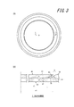
- (B) is a top view of the plate-like member 40 in the susceptor 20 of FIG. 1A is a top view of the susceptor 20 of FIG. 1 (a state in which a plate-like member is placed in the recess of the susceptor body), and FIG.
- FIG. 1B is a cross-sectional view taken along line II of FIG.
- A is a top view of a susceptor according to another embodiment of the present invention (a state where a plate-like member is placed in a recess of the susceptor body), and (B) is a sectional view taken along line II-II of (A). It is.
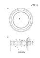
- (A) is a top view of a susceptor according to still another embodiment of the present invention (a state where a plate-like member is placed in the recess of the susceptor body), and (B) is a cross-sectional view taken along line III-III of (A).
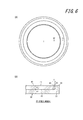
- FIG. 1 is a top view of a susceptor according to a comparative example (a state where a plate-like member is placed in a recess of the susceptor body), and (B) is a cross-sectional view taken along line IV-IV in (A).
- (A) is an exploded perspective view of the susceptor support shaft 50, and (B) is an exploded perspective view of the elevating shaft 60.
- It is a schematic diagram of the epitaxial growth apparatus 100 by one Embodiment of this invention, and the state (at the time of vapor phase growth) with which the wafer W was mounted in the susceptor is shown.
- FIG. 1 is a schematic diagram of an epitaxial growth apparatus 100 according to an embodiment of the present invention, showing a state where a disk-shaped member 40 lifts a wafer W.
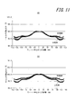
- FIG. It is a schematic diagram of the conventional epitaxial growth apparatus 200, and shows the state (during vapor phase growth) in which the lift pins 40 are lowered with respect to the susceptor 20. It is a graph which shows the in-plane temperature distribution of a wafer, (A) is a comparative example and invention example 1, (B) contrasts a comparative example and invention example 2.
- FIGS. 8 and 9 an epitaxial growth apparatus 100 according to an embodiment of the present invention will be described.
- a susceptor 20 included in the epitaxial growth apparatus 100 according to an embodiment of the present invention will be described with reference to FIGS.
- the epitaxial growth apparatus 100 shown in FIGS. 8 and 9 includes a chamber 10, a heating lamp 14, a susceptor 20 also shown in FIGS. 1 and 2, a susceptor support shaft 50 also shown in FIG. And a lifting shaft 60 also shown in B).
- the chamber 10 includes an upper dome 11, a lower dome 12, and a dome mounting body 13, and the chamber 10 defines an epitaxial film forming chamber.
- the chamber 10 is provided with a gas supply port 15 and a gas discharge port 16 for supplying and discharging the reaction gas at positions opposite to the side surfaces thereof.
- the heating lamps 14 are disposed in the upper region and the lower region of the chamber 10, and generally, a halogen lamp or an infrared lamp that has a high temperature raising / lowering speed and excellent temperature controllability is used.
- the susceptor 20 is a disk-shaped member for placing the wafer W inside the chamber 10.
- the susceptor 20 can be made of carbon graphite (graphite) as a base material and the surface thereof coated with silicon carbide.
- a counterbore portion 21 on which the wafer W is placed is formed on the front surface of the susceptor 20.
- the diameter of the counterbore portion 21 at the open end may be appropriately set in consideration of the diameter of the wafer W, and is usually made larger by about 1.0 to 2.0 mm than the diameter of the wafer W.
- a susceptor 20 includes a susceptor body 30 and a plate-like member 40 placed in a recess 31 provided at the center of the front surface of the susceptor body.
- the front surface of susceptor main body 30 includes front surface outermost peripheral portion 32, wafer support surface 32A, and vertical wall surface 32B.
- the front surface intermediate portion 33, the inclined surface 34, and the front surface center portion 35 are included.
- the front outermost peripheral portion 32 is located around the spot facing portion 21 shown in FIG.
- the wafer support surface 32A is an inclined surface that constitutes a part of a spot facing portion that is positioned inside the outermost peripheral portion 32 of the front surface and supports the peripheral edge of the back surface of the wafer W by line contact.
- the vertical wall surface 32B is a wall surface constituting a part of a spot facing portion that is continuous from the inner peripheral end of the wafer support surface 32A.
- the front surface intermediate portion 33 is continuous from the vertical wall surface 32 ⁇ / b> B and constitutes a part of the bottom surface of the spot facing portion 21.
- the front surface center portion 35 is located inside the front surface intermediate portion 33 and constitutes the bottom surface of the recess 31.
- the inclined surface 34 is a characteristic portion of the present embodiment described later, and is located between the front surface intermediate portion 33 and the front surface center portion 35.
- the susceptor body 30 is provided with three through holes 36 that are concentrically arranged at 120 ° equal intervals and penetrate the front surface center portion 35 and the back surface in the vertical direction. A lift pin 44 described later is inserted into the three through holes 36.
- the disk-shaped member 40 has a front surface 41 and a back surface 42, and is formed in the recess 31 with a minimum clearance (clearance). It is a disk-shaped member to be placed.
- the front surface 41 constitutes a part of the bottom surface of the spot facing portion 21, and the back surface 42 contacts the front surface center portion 35 (the bottom surface of the recess) of the susceptor body. Supported.
- the peripheral edge connecting the front surface 41 and the back surface 42 is an inclined surface 43, which is a feature of this embodiment described later.
- Three lift pins 44 extend from the back surface 42.
- the three lift pins 44 are respectively inserted into three through holes 36 provided in the susceptor body.
- the lift pin 44 is lifted and lowered in the vertical direction by a lift shaft 60 to be described later, so that the disk-shaped member 40 can be attached to and detached from the susceptor body 30 while supporting the back surface 42 of the disk-shaped member. This operation will be described later.
- the lift pins 44 are preferably located in a region away from the center of the back surface 42 of the disk-shaped member by 50% or more of the radius of the back surface. In the present embodiment, the lift pins 44 are fixed to the plate-like member 40, but the lift pins 44 may not be fixed to the plate-like member 40.
- the bottom surface of the spot facing portion 21 is one of the front surface of the susceptor body, which is located around the front surface 41 of the plate-like member and the recess 31. Part (specifically, the front surface intermediate part 33). That is, in the state where the plate-like member 40 is placed in the recess 31 and the wafer W is placed on the spot facing portion 21, the front surface 41 of the plate-like member of the surface of the spot facing portion 21 and the susceptor The front surface intermediate portion 33 of the main body faces the back surface of the wafer W while being separated.
- the wafer W when the wafer W is placed on the spot facing portion 21 and when the wafer W is unloaded from the spot facing portion 21 (that is, the wafer W is transported).
- the susceptor main body 30 and the disk-shaped member 40 are separated from each other in the vertical direction, and the front surface 41 of the disk-shaped member lifted by the lift pins 44 supports at least the center portion of the back surface of the wafer W by surface contact. Function as. Therefore, generation of wrinkles due to lift pins on the back surface of the wafer W can be suppressed.
- the “center portion of the back surface of the wafer” means a region on the back surface of the wafer that is 50% or less of the wafer radius from the wafer center.
- the center of the counterbore 21 coincides with the center of the recess 31 in the front view of the susceptor body 30, that is, the recess 31 is positioned without being eccentric from the counterbore 21.
- the radius of the front surface 41 of the plate-like member is 50% or more of the wafer radius.
- the radius of the front surface 41 of the disk-shaped member is preferably 90% or less of the wafer radius.
- the wafer W supported by the disk-like member 40 is supported at the outer peripheral portion of the back surface of the wafer W by the wafer support portion 72 of the U-shaped transfer blade 70 inserted from the direction shown in FIG. It is conveyed outside. This is because if the radius of the front surface 41 exceeds 90% of the wafer radius, it is difficult to support the wafer W by the transfer blade 70.
- the surface portion of the disk-shaped member 40 or the entire disk-shaped member 40 is made of a soft material (glassy carbon). This is because the generation of scratches when supporting the back surface of the wafer W in surface contact can be suppressed.
- the bottom of the recess 31 of the susceptor body and the plate-like member 40 have a perforated structure. This is because hydrogen gas wrapping around the back surface of the wafer W can be promoted, and halo generation on the back surface of the wafer can be suppressed.
- the susceptor support shaft 50 supports the susceptor 20 from below in the chamber 10, and includes a main column 52, three arms 54, and three support pins 58.
- the main column 52 is disposed substantially coaxially with the center of the susceptor.
- the three arms 54 extend radially from the main column 52 below the peripheral edge of the susceptor 20, and have through holes 56 penetrating in the vertical direction.
- the “periphery of the susceptor” means a region that is 80% or more outside the susceptor radius from the susceptor center.
- the support pins 58 are respectively provided at the tips of the three arms 54 and directly support the susceptor 20.
- the support pin 58 supports the peripheral edge of the back surface of the susceptor.
- Three lift pins 44 are respectively inserted into the three through holes 56.
- the susceptor support shaft 50 is preferably made of quartz, and particularly preferably made of synthetic quartz.
- the tip portion of the support pin 58 is preferably composed of the same silicon carbide as the susceptor 20.
- the lifting shaft 60 as the lifting mechanism defines a hollow that accommodates the main column 52 of the susceptor support shaft, and the main column 62 that shares the rotation axis with the main column 32, and this
- the three pillars 64 branched at the tips of the main pillars 62 are supported, and the lower ends of the lift pins 44 are respectively supported by the tips 66 of the pillars 64.
- the lifting shaft 60 is preferably made of quartz. The lift pin 44 can be moved up and down by the vertical shaft 60 moving vertically up and down along the main column 52 of the susceptor support shaft.
- the wafer W supported by the transfer blade 70 shown in FIG. 2B and loaded into the chamber 10 is temporarily placed on the front surface 41 of the plate-like member 40 lifted by the lift pins 44.
- the lift pin 44 is moved upward through the lift movement of the lift shaft 60 that supports these lower ends.
- the susceptor body 30 is moved to the position of the plate-like member 40, and the wafer W is placed on the counterbore portion 21 of the susceptor 20. Thereafter, the wafer W is heated to a temperature of 1000 ° C. or more by the heating lamp 14, while a reactive gas is supplied from the gas supply port 15 into the chamber 10 to vapor-phase grow an epitaxial film having a predetermined thickness. Manufacture wafers.
- the susceptor support shaft 50 is rotated about the main column 52 as a rotation axis, thereby rotating the susceptor 20 and the wafer W thereon.
- the susceptor main body 30 is lowered by lowering the susceptor support shaft 50. This lowering is performed until the lift pins 44 are supported by the elevating shaft 60 and the disk-shaped member 40 is separated from the susceptor main body 30, and the epitaxial wafer after manufacture is transferred to the front surface of the disk-shaped member 40 supported by the lift pins 44. 41 is supported.
- the transfer blade 70 is introduced into the chamber 10, the lift pins 44 are lowered, and an epitaxial wafer is placed on the wafer support portion 72 of the transfer blade. In this way, the epitaxial wafer is transferred from the disk-shaped member 40 to the transfer blade 70. Thereafter, the epitaxial wafer is carried out of the chamber 10 together with the transfer blade 70.
- the peripheral edge of the disk-shaped member 40 is disk-shaped toward the back surface (that is, vertically downward) from the front surface of the susceptor.
- FIG. 6 the peripheral edge of the disk-shaped member 40 is a vertical surface 49, and the peripheral edge of the concave portion of the susceptor body 30 is also the vertical surface 39.
- the space between the plate-like member 40 and the susceptor body 30 extends straight in the vertical direction, and the space (gap) is largely present directly under the wafer W.
- this gap is set to a minimum interval (for example, about 0.5 to 1.0 mm) necessary for accommodating the disc-like member 40 in the recess 31, the in-plane temperature distribution of the wafer W during the vapor phase growth is obtained.
- the in-plane film thickness distribution of the epitaxially grown epitaxial film is made non-uniform.
- the space between the plate-like member 40 and the susceptor body 30 enters the center side of the plate-like member as it goes downward in the vertical direction.
- size of the clearance gap located just under the wafer W can be made small compared with FIG. 6, As a result, the nonuniformity of the in-plane temperature distribution of the wafer W can be suppressed.
- FIG. 3A is a vertical cross-sectional view (II cross-sectional view) including the center of the susceptor in this state. The same applies to FIG. 6 and FIGS.
- the thickness t1 of the plate-like member 40 is preferably 0.5 mm or more and 3.0 mm or less. From the viewpoint of reducing the size of the gap located directly under the wafer W, it is preferable that the thickness t1 is small. However, if the thickness is less than 0.5 mm, the strength may be insufficient. Further, when the thickness t1 exceeds 3.0 mm, it is difficult to obtain the strength of the susceptor body 30.
- the radius r4 of the front surface 41 of the plate-like member is 50% or more and preferably 90% or less of the wafer radius as described above.
- the radius r3 of the back surface 42 of the disk-shaped member is preferably smaller by about 1.0 to 5.0 mm than r4.
- the inclined surface 43 and the inclined surface 34 preferably have the same inclination angle, and the inclination angle with respect to the vertical direction is preferably 30 to 45 degrees.
- the shape of the peripheral portion of the plate-like member 40 and the shape of the peripheral portion of the concave portion of the susceptor main body 30 are not limited to those shown in FIG. 3B, and the space between the plate-like member 40 and the susceptor main body 30 is not limited.
- the effect of the present invention can be obtained if it is designed to enter the center side of the disk-shaped member as it goes downward in the vertical direction.
- the peripheral part of the disk-shaped member 40 is a vertical surface 45A continuous from the front surface 41, and the slope that is continuous from the vertical surface 45A and enters the center side of the disk-shaped member as it goes downward in the vertical direction.
- the peripheral edge of the concave portion of the susceptor body 30 is also a vertical surface 37A continuous from the front surface intermediate portion 33, and an inclined surface 37B continuous from the vertical surface 37A and entering the center side of the plate-like member as it goes downward in the vertical direction.
- the size of the gap located immediately below the wafer W can be made smaller than that in FIG. 6, and as a result, the in-plane temperature distribution of the wafer W can be suppressed.
- the end of the plate-like member 40 is pointed and the strength may be insufficient, but in the case of FIG. 4B, the strength is not impaired.
- the height of the vertical surface 45A and the vertical surface 37A is preferably 20 to 50% of the thickness t1 of the plate-like member 40. If it is less than 20%, the strength may be insufficient, and if it exceeds 50%, the effect of suppressing unevenness of the in-plane temperature distribution of the wafer W may be insufficient.
- the inclined surface 45B and the inclined surface 37B preferably have the same inclination angle, and the inclination angle with respect to the vertical direction is preferably 30 to 45 degrees as in FIG.
- FIGS. 5A and 5B show still another embodiment.
- the peripheral edge portion of the concave portion of the susceptor body 30 is continuous from the first vertical surface 38A that continues from the front surface center portion 35, the horizontal surface 38B that continues from the first vertical surface 38A, and the horizontal surface 38B. And it has a level
- the disk-shaped member 40 has a first portion 46 having a first radius r1 and a second portion 47 having a second radius r2 larger than r1 on the first portion.
- the peripheral portion of the disk-shaped member 40 includes a first vertical surface 46A that is an outer peripheral portion of the first portion, a second vertical surface 47A that is an outer peripheral portion of the second portion, and a horizontal plane 48 positioned therebetween. Consists of.
- the step portion supports the peripheral portion 47B of the second portion. That is, the horizontal plane 48 and the horizontal plane 38B are in contact with each other.
- the space between the disk-shaped member 40 and the susceptor body 30 gradually enters the center side of the disk-shaped member as it goes downward in the vertical direction, so the size of the gap located directly below the wafer W is large. 6 can be made smaller than that in FIG. 6, and as a result, the in-plane temperature distribution of the wafer W can be suppressed.
- the height of the second vertical surface 47A of the plate-like member and the second vertical surface 38C of the susceptor body is preferably the same, and can be about 20 to 50% of the thickness t1 of the plate-like member 40. .
- the first vertical surface 46A of the plate-like member and the first vertical surface 38A of the susceptor body preferably have the same height.
- the radius r2 of the second portion (that is, the radius of the front surface 41 of the plate-like member) is 50% or more and 90% or less of the wafer radius as described above.
- the radius r1 of the first portion (that is, the radius of the back surface 42 of the plate-like member) is preferably about 1.0 to 5.0 mm smaller than r2.
- the width of the stepped portion (horizontal plane 38B) is preferably equal to (r2-r1).
- FIG. 5B An epitaxial silicon wafer was manufactured in the same manner as in Invention Example 1 except that the susceptor shown in FIG. 5 was used.
- a silicon wafer was introduced into the chamber and placed on the susceptor by the method described above. Subsequently, after hydrogen baking was performed at 1150 ° C. in a hydrogen gas atmosphere, a silicon epitaxial film was grown on the surface of the silicon wafer by 4 ⁇ m at 1150 ° C. to obtain an epitaxial silicon wafer.
- trichlorosilane gas was used as the source gas
- diborane gas was used as the dopant gas
- hydrogen gas was used as the carrier gas.
- the epitaxial silicon wafer was carried out of the chamber by the method described above.
- the susceptor and epitaxial growth apparatus of the present invention are suitable for the production of epitaxial wafers because they do not generate wrinkles due to lift pins on the back surface of the wafer and can suppress non-uniform temperature distribution in the wafer surface. Applicable to.
Landscapes
- Chemical & Material Sciences (AREA)
- Engineering & Computer Science (AREA)
- Materials Engineering (AREA)
- Metallurgy (AREA)
- Organic Chemistry (AREA)
- Chemical Kinetics & Catalysis (AREA)
- General Chemical & Material Sciences (AREA)
- Crystallography & Structural Chemistry (AREA)
- Mechanical Engineering (AREA)
- Container, Conveyance, Adherence, Positioning, Of Wafer (AREA)
- Chemical Vapour Deposition (AREA)
- Crystals, And After-Treatments Of Crystals (AREA)
Abstract
Description
(1)エピタキシャル成長装置内でウェーハを載置するためのサセプタであって、
前記サセプタのおもて面には、前記ウェーハが載置される座ぐり部が形成され、
前記サセプタは、サセプタ本体と、該サセプタ本体のおもて面の中心部に設けられた凹部に載置された盤状部材とを有し、
前記座ぐり部の底面が、前記盤状部材のおもて面と、前記凹部の周囲に位置する、前記サセプタ本体のおもて面の一部とで構成され、
前記サセプタ本体には、前記盤状部材の裏面を支持して前記盤状部材を昇降させるリフトピンを挿通するための貫通孔が設けられ、
前記ウェーハを前記座ぐり部に載置する際、及び、前記ウェーハを前記座ぐり部から搬出する際に、前記リフトピンにより上昇される前記盤状部材のおもて面が、前記ウェーハの裏面の少なくとも中心部を面接触で支持する支持面として機能し、
前記盤状部材が前記凹部に載置された状態での、前記盤状部材と前記サセプタ本体との離間空間が、前記サセプタのおもて面から裏面に向かうほど、前記盤状部材の中心側に入り込むことを特徴とするサセプタ。
前記盤状部材は、第1半径r1の第1部分と、該第1部分の上でr1よりも大きい第2半径r2の第2部分とを有し、
前記段差部が、前記第2部分の周縁部を支持する上記(1)に記載のサセプタ。
前記リフトピンの下端部を支持して前記リフトピンを昇降させる昇降機構と、を有するエピタキシャル成長装置。
図8及び図9に示すエピタキシャル成長装置100は、チャンバ10と、加熱ランプ14と、図1及び図2にも示すサセプタ20と、図7(A)にも示すサセプタサポートシャフト50と、図7(B)にも示す昇降シャフト60とを有する。
チャンバ10は、上部ドーム11、下部ドーム12及びドーム取付体13を含み、このチャンバ10がエピタキシャル膜形成室を区画する。チャンバ10には、その側面の対向する位置に反応ガスの供給及び排出を行うガス供給口15及びガス排出口16が設けられる。
加熱ランプ14は、チャンバ10の上側領域および下側領域に配置され、一般に、昇降温速度が速く、温度制御性に優れた、ハロゲンランプや赤外ランプが用いられる。
図1及び図2を参照して、サセプタ20の主要な構成を説明する。サセプタ20は、チャンバ10の内部でウェーハWを載置するための円盤状の部材である。サセプタ20は、カーボングラファイト(黒鉛)を母材とし、その表面を炭化ケイ素でコーティングしたものを使用することができる。図1(A)及び(B)を参照して、サセプタ20のおもて面には、ウェーハWが載置される座ぐり部21が形成されている。座ぐり部21の開口端における直径は、ウェーハWの直径を考慮して適宜設定すればよく、通常、ウェーハWの直径よりも1.0~2.0mm程度大きくする。
図7(A)を参照して、サセプタサポートシャフト50は、チャンバ10内でサセプタ20を下方から支持するものであり、主柱52と、3本のアーム54と、3本の支持ピン58とを有する。主柱52は、サセプタの中心とほぼ同軸上に配置される。3本のアーム54は、主柱52からサセプタ20の周縁部下方に放射状に延び、それぞれ鉛直方向に貫通する貫通孔56を有する。なお、本明細書において「サセプタの周縁部」とは、サセプタ中心からサセプタ半径の80%以上外側の領域を意味する。支持ピン58は、3本のアーム54の先端にそれぞれ設けられ、サセプタ20を直接支持する。すなわち、支持ピン58は、サセプタの裏面周縁部を支持する。3つの貫通孔56には、3本のリフトピン44がそれぞれ挿通される。サセプタサポートシャフト50は、石英で構成することが望ましく、特に合成石英で構成することが望ましい。ただし、支持ピン58の先端部分は、サセプタ20と同じ炭化ケイ素で構成することが好ましい。
図7(B)に示すように、昇降機構としての昇降シャフト60は、サセプタサポートシャフトの主柱52を収容する中空を区画し、この主柱32と回転軸を共有する主柱62と、この主柱62の先端で分岐する3本の支柱64とを有し、これら支柱64の先端部66でリフトピン44の下端部をそれぞれ支持する。昇降シャフト60は石英で構成されることが好ましい。昇降シャフト60が、サセプタサポートシャフトの主柱52に沿って鉛直方向上下に動くことにより、リフトピン44を昇降させることができる。
次に、チャンバ10内へのウェーハWの搬入、ウェーハWへのエピタキシャル膜の気相成長、及び製造されたエピタキシャルウェーハのチャンバ10外への搬出の一連の動作を、図8及び図9を適宜参照して説明する。
ここで本発明の特徴的構成である、サセプタ本体30と盤状部材40との離間状態について詳細に説明する。
図1~3に示すサセプタと、図8,9に示すエピタキシャル成長装置を用いて、上記した手順に従ってエピタキシャルシリコンウェーハを製造した。図3(B)において、半径r3=120mm、半径r4=123mm、厚さt1=2.0mm、厚さt2=2.3mm、隙間の間隔G=1.0mmとした。エピタキシャルウェーハの基板としては、ボロンドープされた直径300mmのシリコンウェーハを用いた。
図5に示すサセプタを用いた以外は発明例1と同様にして、エピタキシャルシリコンウェーハを製造した。図5(B)において、半径r1=121mm、半径r2=123mm、厚さt1=2.0mm、厚さt2=2.3mm、隙間の間隔G=1.0mmとした。
図6に示すサセプタを用いた以外は発明例1と同様にして、エピタキシャルシリコンウェーハを製造した。図6(B)において、厚さt1=2.0mm、厚さt2=2.3mm、隙間の間隔G=1.0mmとした。盤状部材の半径は120mmとした。
エピタキシャルウェーハの製造は、シリコンウェーハをチャンバ内に導入し、既述の方法でサセプタ上に載置した。続いて、水素ガス雰囲気下で1150℃で水素ベークを行った後、1150℃にて、シリコンウェーハの表面にシリコンエピタキシャル膜を4μm成長させてエピタキシャルシリコンウェーハを得た。ここで、原料ソースガスとしてはトリクロロシランガスを用い、また、ドーパントガスとしてジボランガス、キャリアガスとして水素ガスを用いた。その後、既述の方法で、エピタキシャルシリコンウェーハをチャンバ外へ搬出した。
発明例及び比較例で製造したエピタキシャルウェーハについて、表面検査装置(KLA-Tencor社製:Surfscan SP-2)を用いて、DCOモードで、リフトピンの位置に対応する裏面領域を観察し、レーザー反射の設定値以上の散乱強度を有する領域の面積(ピンマーク強度)を測定し、エピタキシャルウェーハ裏面のリフトピン起因の疵付きを評価した。その結果、比較例、発明例1,2とも0mm2であり、エピタキシャルウェーハの裏面にリフトピンに起因する疵は確認されなかった。
発明例及び比較例で製造したエピタキシャルウェーハについて、表面検査装置(KLA-Tencor社製:Surfscan SP-2)を用いてヘイズレベルを計測した。ヘイズレベルはウェーハ面内の温度に比例することが知られているため、この値からウェーハ面内の温度分布を算出比較した。結果を図11に示す。
10 チャンバ
11 上部ドーム
12 下部ドーム
13 ドーム取付体
14 加熱ランプ
15 ガス供給口
16 ガス排出口
20 サセプタ
21 座ぐり部
30 サセプタ本体
31 凹部
32 サセプタ本体のおもて面最外周部
32A ウェーハ支持面
32B 縦壁面
33 サセプタ本体のおもて面中間部
34 傾斜面
35 サセプタ本体のおもて面中心部(凹部の底面)
36 貫通孔
37A 鉛直面
37B 傾斜面
38A 第1鉛直面
38B 水平面
38C 第2鉛直面
40 盤状部材
41 盤状部材のおもて面
42 盤状部材の裏面
43 傾斜面
44 リフトピン
45A 鉛直面
45B 傾斜面
46 第1部分
46A 第1鉛直面
47 第2部分
47A 第2鉛直面
47B 第2部分の周縁部
48 水平面
50 サセプタサポートシャフト
52 主柱
54 アーム
56 貫通孔
58 支持ピン
60 昇降シャフト
62 主柱
64 支柱
66 支柱の先端部
70 ウェーハ搬送用ブレード
72 ウェーハ支持部
W ウェーハ
Claims (5)
- エピタキシャル成長装置内でウェーハを載置するためのサセプタであって、
前記サセプタのおもて面に、前記ウェーハが載置される座ぐり部が形成され、
前記サセプタは、サセプタ本体と、該サセプタ本体のおもて面の中心部に設けられた凹部に載置された盤状部材とを有し、
前記座ぐり部の底面が、前記盤状部材のおもて面と、前記凹部の周囲に位置する、前記サセプタ本体のおもて面の一部とで構成され、
前記サセプタ本体には、前記盤状部材の裏面を支持して前記盤状部材を昇降させるリフトピンを挿通するための貫通孔が設けられ、
前記ウェーハを前記座ぐり部に載置する際、及び、前記ウェーハを前記座ぐり部から搬出する際に、前記リフトピンにより上昇される前記盤状部材のおもて面が、前記ウェーハの裏面の少なくとも中心部を面接触で支持する支持面として機能し、
前記盤状部材が前記凹部に載置された状態での、前記盤状部材と前記サセプタ本体との離間空間が、前記サセプタのおもて面から裏面に向かうほど、前記盤状部材の中心側に入り込むことを特徴とするサセプタ。 - 前記盤状部材の周縁部及び前記サセプタ本体の前記凹部の周縁部が、前記サセプタのおもて面から裏面に向かうほど前記盤状部材の中心側に入り込む傾斜面を有する、請求項1に記載のサセプタ。
- 前記サセプタ本体の前記凹部の周縁部が段差部を有し、
前記盤状部材は、第1半径r1の第1部分と、該第1部分の上でr1よりも大きい第2半径r2の第2部分とを有し、
前記段差部が、前記第2部分の周縁部を支持する請求項1に記載のサセプタ。 - 前記リフトピンが前記盤状部材に固定されている請求項1~3のいずれか一項に記載のサセプタ。
- 請求項1~4のいずれか一項に記載のサセプタと、
前記リフトピンの下端部を支持して前記リフトピンを昇降させる昇降機構と、を有するエピタキシャル成長装置。
Priority Applications (3)
| Application Number | Priority Date | Filing Date | Title |
|---|---|---|---|
| CN201680024187.6A CN107851561B (zh) | 2015-04-27 | 2016-04-22 | 基座及外延生长装置 |
| KR1020177029627A KR102035120B1 (ko) | 2015-04-27 | 2016-04-22 | 서셉터 및 에피택셜 성장 장치 |
| US15/567,148 US11274371B2 (en) | 2015-04-27 | 2016-04-22 | Susceptor and epitaxial growth device |
Applications Claiming Priority (2)
| Application Number | Priority Date | Filing Date | Title |
|---|---|---|---|
| JP2015-090559 | 2015-04-27 | ||
| JP2015090559A JP6424726B2 (ja) | 2015-04-27 | 2015-04-27 | サセプタ及びエピタキシャル成長装置 |
Publications (1)
| Publication Number | Publication Date |
|---|---|
| WO2016174859A1 true WO2016174859A1 (ja) | 2016-11-03 |
Family
ID=57199086
Family Applications (1)
| Application Number | Title | Priority Date | Filing Date |
|---|---|---|---|
| PCT/JP2016/002164 Ceased WO2016174859A1 (ja) | 2015-04-27 | 2016-04-22 | サセプタ及びエピタキシャル成長装置 |
Country Status (6)
| Country | Link |
|---|---|
| US (1) | US11274371B2 (ja) |
| JP (1) | JP6424726B2 (ja) |
| KR (1) | KR102035120B1 (ja) |
| CN (1) | CN107851561B (ja) |
| TW (1) | TWI627701B (ja) |
| WO (1) | WO2016174859A1 (ja) |
Cited By (2)
| Publication number | Priority date | Publication date | Assignee | Title |
|---|---|---|---|---|
| CN113053799A (zh) * | 2019-12-26 | 2021-06-29 | 昭和电工株式会社 | 基座 |
| CN115852478A (zh) * | 2022-12-15 | 2023-03-28 | 西安奕斯伟材料科技有限公司 | 用于硅片的外延生长的基座及装置 |
Families Citing this family (15)
| Publication number | Priority date | Publication date | Assignee | Title |
|---|---|---|---|---|
| JP6532424B2 (ja) * | 2016-03-30 | 2019-06-19 | 三菱電機株式会社 | 基板設置部材、ウェハプレート、およびSiCエピタキシャル基板の製造方法 |
| DE112017006987B4 (de) | 2017-02-02 | 2022-09-08 | Sumco Corporation | Hebestift, Epitaxiewachstumsvorrichtung und Verfahren zur Herstellung von Siliziumepitaxiewafern unter Verwendung des Hebestiftes |
| US11702748B2 (en) * | 2017-03-03 | 2023-07-18 | Lam Research Corporation | Wafer level uniformity control in remote plasma film deposition |
| JP7451490B2 (ja) * | 2018-07-30 | 2024-03-18 | ノードソン コーポレーション | プラズマを用いたワーク処理用のシステム |
| DE102019132933A1 (de) * | 2018-12-10 | 2020-06-10 | Showa Denko K.K. | Suszeptor und vorrichtung zur chemischen gasphasenabscheidung |
| CN109686684B (zh) * | 2018-12-27 | 2020-08-28 | 西安奕斯伟硅片技术有限公司 | 一种硅晶圆的加工方法、控制装置及外延反应设备 |
| JP7188250B2 (ja) * | 2019-04-11 | 2022-12-13 | 株式会社Sumco | 気相成長装置及びこれに用いられるキャリア |
| US20220254676A1 (en) * | 2019-07-25 | 2022-08-11 | Epicrew Corporation | Process chamber of epitaxial growth apparatus |
| CN110943029A (zh) * | 2019-12-30 | 2020-03-31 | 浙江求是半导体设备有限公司 | 一种用于半导体外延系统的双环式基座 |
| TWD235071S (zh) * | 2020-12-10 | 2024-12-01 | 日商紐富來科技股份有限公司 (日本) | 頂板 |
| CN113629002A (zh) * | 2021-08-18 | 2021-11-09 | 盛吉盛(宁波)半导体科技有限公司 | 一种外延膜生长设备的基座支撑装置及其使用方法 |
| CN114093815B (zh) * | 2021-11-12 | 2024-10-18 | 绍兴同芯成集成电路有限公司 | 一种背面键合玻璃载板的igbt晶圆加工工艺 |
| CN114232084B (zh) * | 2021-12-23 | 2023-06-06 | 西安奕斯伟材料科技有限公司 | 基座支撑结构和外延生长装置 |
| CN114411247B (zh) * | 2022-01-21 | 2023-05-16 | 深圳市纳设智能装备有限公司 | 一种外延反应设备 |
| JP7810618B2 (ja) * | 2022-08-23 | 2026-02-03 | ユナイテッド・セミコンダクター・ジャパン株式会社 | ウェーハ支持板及びそれを備えた半導体製造装置 |
Citations (2)
| Publication number | Priority date | Publication date | Assignee | Title |
|---|---|---|---|---|
| JP2009270143A (ja) * | 2008-05-02 | 2009-11-19 | Nuflare Technology Inc | サセプタ、半導体製造装置及び半導体製造方法 |
| JP2010074037A (ja) * | 2008-09-22 | 2010-04-02 | Nuflare Technology Inc | サセプタ、半導体製造装置および半導体製造方法 |
Family Cites Families (20)
| Publication number | Priority date | Publication date | Assignee | Title |
|---|---|---|---|---|
| JP3333020B2 (ja) | 1993-10-29 | 2002-10-07 | 東京エレクトロン株式会社 | 処理方法及び処理装置 |
| JPH08288373A (ja) * | 1995-04-18 | 1996-11-01 | Touyoko Kagaku Kk | 基板脱着装置 |
| JPH08316222A (ja) | 1995-05-19 | 1996-11-29 | Tokyo Electron Ltd | 熱処理方法及びその装置 |
| US5584936A (en) * | 1995-12-14 | 1996-12-17 | Cvd, Incorporated | Susceptor for semiconductor wafer processing |
| JPH11163102A (ja) * | 1997-11-27 | 1999-06-18 | Kokusai Electric Co Ltd | 半導体製造装置用サセプタ |
| JP2001176808A (ja) * | 1999-12-21 | 2001-06-29 | Toshiba Ceramics Co Ltd | 気相薄膜成長装置におけるウエハ搬送方法およびそれに用いるウエハ支持部材 |
| JP2001313329A (ja) | 2000-04-28 | 2001-11-09 | Applied Materials Inc | 半導体製造装置におけるウェハ支持装置 |
| KR20020090491A (ko) * | 2001-05-28 | 2002-12-05 | 삼성전자 주식회사 | 반도체 웨이퍼 세정장치 |
| JP2004063865A (ja) | 2002-07-30 | 2004-02-26 | Shin Etsu Handotai Co Ltd | サセプタ、気相成長装置およびエピタキシャルウェーハの製造方法 |
| JP4019998B2 (ja) * | 2003-04-14 | 2007-12-12 | 信越半導体株式会社 | サセプタ及び気相成長装置 |
| JP2005197380A (ja) | 2004-01-06 | 2005-07-21 | Sumitomo Mitsubishi Silicon Corp | ウェーハ支持装置 |
| JP2006124758A (ja) * | 2004-10-27 | 2006-05-18 | Komatsu Electronic Metals Co Ltd | サセプタ、エピタキシャルウェーハの製造装置、およびエピタキシャルウェーハの製造方法 |
| JP4850952B2 (ja) * | 2008-02-14 | 2012-01-11 | 東京エレクトロン株式会社 | 液処理装置、液処理方法および記憶媒体 |
| JP5412759B2 (ja) | 2008-07-31 | 2014-02-12 | 株式会社Sumco | エピタキシャルウェーハの保持具及びそのウェーハの製造方法 |
| WO2010109848A1 (ja) * | 2009-03-26 | 2010-09-30 | パナソニック株式会社 | プラズマ処理装置及びプラズマ処理方法 |
| JP5038365B2 (ja) * | 2009-07-01 | 2012-10-03 | 株式会社東芝 | サセプタおよび成膜装置 |
| JP2011146506A (ja) | 2010-01-14 | 2011-07-28 | Sumco Corp | 気相成長装置用サセプタ及び気相成長装置 |
| CN103930985B (zh) * | 2011-10-13 | 2017-03-29 | 株式会社爱发科 | 真空处理装置 |
| KR20140090809A (ko) * | 2013-01-10 | 2014-07-18 | 주식회사 엘지실트론 | 서셉터 지지부를 구비하는 웨이퍼 에피택셜 성장 장치 |
| KR20140092704A (ko) * | 2013-01-16 | 2014-07-24 | 주식회사 엘지실트론 | 서셉터 및 이를 포함하는 에피텍셜 반응기 |
-
2015
- 2015-04-27 JP JP2015090559A patent/JP6424726B2/ja active Active
-
2016
- 2016-03-31 TW TW105110248A patent/TWI627701B/zh active
- 2016-04-22 US US15/567,148 patent/US11274371B2/en active Active
- 2016-04-22 KR KR1020177029627A patent/KR102035120B1/ko active Active
- 2016-04-22 CN CN201680024187.6A patent/CN107851561B/zh active Active
- 2016-04-22 WO PCT/JP2016/002164 patent/WO2016174859A1/ja not_active Ceased
Patent Citations (2)
| Publication number | Priority date | Publication date | Assignee | Title |
|---|---|---|---|---|
| JP2009270143A (ja) * | 2008-05-02 | 2009-11-19 | Nuflare Technology Inc | サセプタ、半導体製造装置及び半導体製造方法 |
| JP2010074037A (ja) * | 2008-09-22 | 2010-04-02 | Nuflare Technology Inc | サセプタ、半導体製造装置および半導体製造方法 |
Cited By (3)
| Publication number | Priority date | Publication date | Assignee | Title |
|---|---|---|---|---|
| CN113053799A (zh) * | 2019-12-26 | 2021-06-29 | 昭和电工株式会社 | 基座 |
| CN113053799B (zh) * | 2019-12-26 | 2024-04-26 | 株式会社力森诺科 | 基座 |
| CN115852478A (zh) * | 2022-12-15 | 2023-03-28 | 西安奕斯伟材料科技有限公司 | 用于硅片的外延生长的基座及装置 |
Also Published As
| Publication number | Publication date |
|---|---|
| CN107851561B (zh) | 2021-08-24 |
| US20180100235A1 (en) | 2018-04-12 |
| KR20170126503A (ko) | 2017-11-17 |
| KR102035120B1 (ko) | 2019-10-22 |
| TWI627701B (zh) | 2018-06-21 |
| JP6424726B2 (ja) | 2018-11-21 |
| JP2016207932A (ja) | 2016-12-08 |
| CN107851561A (zh) | 2018-03-27 |
| TW201705352A (zh) | 2017-02-01 |
| US11274371B2 (en) | 2022-03-15 |
Similar Documents
| Publication | Publication Date | Title |
|---|---|---|
| WO2016174859A1 (ja) | サセプタ及びエピタキシャル成長装置 | |
| JP6288371B2 (ja) | サセプタ、エピタキシャル成長装置、及びエピタキシャルウェーハ | |
| JP5604907B2 (ja) | 気相成長用半導体基板支持サセプタおよびエピタキシャルウェーハ製造装置およびエピタキシャルウェーハの製造方法 | |
| US7615116B2 (en) | Method for producing silicon epitaxial wafer and silicon epitaxial wafer | |
| JP2019047085A (ja) | サセプタ、cvd装置及びエピタキシャルウェハの製造方法 | |
| WO2001033617A1 (en) | Semiconductor-manufacturing apparatus | |
| JP2020053627A (ja) | 気相成長装置、エピタキシャルウェーハの製造方法 | |
| JP6551335B2 (ja) | サセプタサポートシャフト及びエピタキシャル成長装置 | |
| KR101432916B1 (ko) | 웨이퍼 리프트 장치 | |
| JP6428358B2 (ja) | エピタキシャル成長装置及びサセプタサポートシャフト | |
| JP2017076652A (ja) | 基板載置台及び気相成長装置 | |
| JP2018026503A (ja) | サセプタ、エピタキシャル成長装置、及びエピタキシャルウェーハの製造方法 | |
| JP2006041028A (ja) | サセプタ、およびエピタキシャルウェーハの製造方法 | |
| TW201332055A (zh) | 基座 | |
| JP6844529B2 (ja) | エピタキシャルウェーハの製造方法およびエピタキシャルウェーハ | |
| WO2001031700A1 (fr) | Porte-plaquette et dispositif de croissance epitaxiale | |
| JP6233712B2 (ja) | 気相成長装置及び被処理基板の支持構造 | |
| CN114059158A (zh) | 一种用于晶圆外延生长的晶圆支撑杆装置、设备及方法 | |
| KR101436059B1 (ko) | 반도체 제조 장치 및 방법 | |
| JP2024088405A (ja) | 半導体処理部材 | |
| JP2002100667A (ja) | 熱処理用基板支持具 | |
| KR101496674B1 (ko) | 반도체 제조 장치 및 방법 |
Legal Events
| Date | Code | Title | Description |
|---|---|---|---|
| 121 | Ep: the epo has been informed by wipo that ep was designated in this application |
Ref document number: 16786136 Country of ref document: EP Kind code of ref document: A1 |
|
| ENP | Entry into the national phase |
Ref document number: 20177029627 Country of ref document: KR Kind code of ref document: A |
|
| WWE | Wipo information: entry into national phase |
Ref document number: 15567148 Country of ref document: US |
|
| NENP | Non-entry into the national phase |
Ref country code: DE |
|
| 122 | Ep: pct application non-entry in european phase |
Ref document number: 16786136 Country of ref document: EP Kind code of ref document: A1 |