WO2016161725A1 - 移位寄存器单元、栅极驱动装置以及显示装置 - Google Patents
移位寄存器单元、栅极驱动装置以及显示装置 Download PDFInfo
- Publication number
- WO2016161725A1 WO2016161725A1 PCT/CN2015/085941 CN2015085941W WO2016161725A1 WO 2016161725 A1 WO2016161725 A1 WO 2016161725A1 CN 2015085941 W CN2015085941 W CN 2015085941W WO 2016161725 A1 WO2016161725 A1 WO 2016161725A1
- Authority
- WO
- WIPO (PCT)
- Prior art keywords
- pull
- module
- control node
- clock signal
- signal
- Prior art date
- Legal status (The legal status is an assumption and is not a legal conclusion. Google has not performed a legal analysis and makes no representation as to the accuracy of the status listed.)
- Ceased
Links
Images

Classifications
-
- G—PHYSICS
- G09—EDUCATION; CRYPTOGRAPHY; DISPLAY; ADVERTISING; SEALS
- G09G—ARRANGEMENTS OR CIRCUITS FOR CONTROL OF INDICATING DEVICES USING STATIC MEANS TO PRESENT VARIABLE INFORMATION
- G09G3/00—Control arrangements or circuits, of interest only in connection with visual indicators other than cathode-ray tubes
- G09G3/20—Control arrangements or circuits, of interest only in connection with visual indicators other than cathode-ray tubes for presentation of an assembly of a number of characters, e.g. a page, by composing the assembly by combination of individual elements arranged in a matrix no fixed position being assigned to or needed to be assigned to the individual characters or partial characters
- G09G3/34—Control arrangements or circuits, of interest only in connection with visual indicators other than cathode-ray tubes for presentation of an assembly of a number of characters, e.g. a page, by composing the assembly by combination of individual elements arranged in a matrix no fixed position being assigned to or needed to be assigned to the individual characters or partial characters by control of light from an independent source
- G09G3/36—Control arrangements or circuits, of interest only in connection with visual indicators other than cathode-ray tubes for presentation of an assembly of a number of characters, e.g. a page, by composing the assembly by combination of individual elements arranged in a matrix no fixed position being assigned to or needed to be assigned to the individual characters or partial characters by control of light from an independent source using liquid crystals
- G09G3/3611—Control of matrices with row and column drivers
- G09G3/3648—Control of matrices with row and column drivers using an active matrix
-
- G—PHYSICS
- G09—EDUCATION; CRYPTOGRAPHY; DISPLAY; ADVERTISING; SEALS
- G09G—ARRANGEMENTS OR CIRCUITS FOR CONTROL OF INDICATING DEVICES USING STATIC MEANS TO PRESENT VARIABLE INFORMATION
- G09G3/00—Control arrangements or circuits, of interest only in connection with visual indicators other than cathode-ray tubes
- G09G3/20—Control arrangements or circuits, of interest only in connection with visual indicators other than cathode-ray tubes for presentation of an assembly of a number of characters, e.g. a page, by composing the assembly by combination of individual elements arranged in a matrix no fixed position being assigned to or needed to be assigned to the individual characters or partial characters
- G09G3/34—Control arrangements or circuits, of interest only in connection with visual indicators other than cathode-ray tubes for presentation of an assembly of a number of characters, e.g. a page, by composing the assembly by combination of individual elements arranged in a matrix no fixed position being assigned to or needed to be assigned to the individual characters or partial characters by control of light from an independent source
- G09G3/36—Control arrangements or circuits, of interest only in connection with visual indicators other than cathode-ray tubes for presentation of an assembly of a number of characters, e.g. a page, by composing the assembly by combination of individual elements arranged in a matrix no fixed position being assigned to or needed to be assigned to the individual characters or partial characters by control of light from an independent source using liquid crystals
- G09G3/3611—Control of matrices with row and column drivers
- G09G3/3674—Details of drivers for scan electrodes
- G09G3/3677—Details of drivers for scan electrodes suitable for active matrices only
-
- G—PHYSICS
- G11—INFORMATION STORAGE
- G11C—STATIC STORES
- G11C19/00—Digital stores in which the information is moved stepwise, e.g. shift registers
- G11C19/28—Digital stores in which the information is moved stepwise, e.g. shift registers using semiconductor elements
- G11C19/287—Organisation of a multiplicity of shift registers
-
- G—PHYSICS
- G09—EDUCATION; CRYPTOGRAPHY; DISPLAY; ADVERTISING; SEALS
- G09G—ARRANGEMENTS OR CIRCUITS FOR CONTROL OF INDICATING DEVICES USING STATIC MEANS TO PRESENT VARIABLE INFORMATION
- G09G2300/00—Aspects of the constitution of display devices
- G09G2300/04—Structural and physical details of display devices
-
- G—PHYSICS
- G09—EDUCATION; CRYPTOGRAPHY; DISPLAY; ADVERTISING; SEALS
- G09G—ARRANGEMENTS OR CIRCUITS FOR CONTROL OF INDICATING DEVICES USING STATIC MEANS TO PRESENT VARIABLE INFORMATION
- G09G2310/00—Command of the display device
- G09G2310/02—Addressing, scanning or driving the display screen or processing steps related thereto
- G09G2310/0264—Details of driving circuits
- G09G2310/0286—Details of a shift registers arranged for use in a driving circuit
-
- G—PHYSICS
- G09—EDUCATION; CRYPTOGRAPHY; DISPLAY; ADVERTISING; SEALS
- G09G—ARRANGEMENTS OR CIRCUITS FOR CONTROL OF INDICATING DEVICES USING STATIC MEANS TO PRESENT VARIABLE INFORMATION
- G09G2310/00—Command of the display device
- G09G2310/08—Details of timing specific for flat panels, other than clock recovery
Definitions
- the present disclosure relates to the field of display technology, and more particularly to a shift register unit, and a gate driving device and a display device using the same.
- the GOA circuit generally includes a plurality of cascaded shift register units, each shift register unit being respectively connected to a shift register unit of an adjacent row, each shift register unit corresponding to a row of gate lines, each shift register The unit supplies the output signal to the next shift register unit while outputting the gate drive signal to ensure that the next shift register unit realizes the output of the gate drive signal in the next clock cycle.
- a thin film crystal diode (TFT) is usually used to pull the potential of the output signal of the shift register unit to a low level.
- the duty cycle of the pull-down TFT is usually greater than 99%, which causes the pull-down TFT to age rapidly, and the overall circuit has problems that affect the life of the product.
- An object of the present disclosure is to provide a shift register unit, and a gate driving device and a display device using the same, to partially or completely solve the above disadvantages.
- a shift register unit including a pull-up module, an input module, a reset module, a first pull-down module, a second pull-down module, a first control module, a second control module, and a A state clearing module and a second state clearing module.
- the pull-up module is connected to the first clock signal port, the pull-up control node (PU), and the signal output end, and is configured to output the signal output end according to the potential of the pull-up control node and the first clock signal input by the first clock signal port
- the signal pull-up is high level
- the pull-up control node is a connection point between the pull-up module and the input module
- the input module is connected to the signal input end and the pull-up control node, and is used for controlling the pull-up according to the signal input by the signal input end
- the reset module is connected to the reset signal end, the first clock signal port, the pull-up control node, and the signal output end, and is used for pulling up and controlling according to the signal input by the reset signal terminal and the first clock signal
- the potential of the node and the signal outputted by the signal output are pulled down to a low level
- the first pull-down module is connected to the first clock signal port, the second clock signal port of the second clock signal,
- the first control module is connected to the signal output end and the first control node, and is configured to disable the first pull-down module when the signal output end outputs a signal; the second control module a signal input end and a second control node, configured to disable the second pull-down module when inputting a signal at the signal input end; the first state clearing module is coupled to the second clock signal port and the first control node for the second clock signal potential The state of the first pull-down module is cleared when it is high; the second state clearing module is connected to the first clock signal port and the second control node for clearing the state of the second pull-down module when the first clock signal potential is high.
- the shift register unit uses the first clock signal and the second clock signal to alternately pull down the first pull-down module and the second pull-down module, thereby maintaining the stability of the output signal. Moreover, the duty ratio of all TFTs in the circuit structure is less than 50%, thereby greatly improving the lifetime of the TFT.
- a gate driving apparatus including a plurality of the shift register units, wherein the plurality of shift register units are cascaded with each other except for a first shift register unit and Outside the last shift register unit, the signal output terminals of each of the other shift register units are connected to the input terminal of the next shift register unit adjacent thereto and the reset signal terminal of the previous shift register unit adjacent thereto.
- the signal input end of the first shift register unit inputs a frame start signal
- the signal output end is connected to a signal input end of the second shift register unit
- the signal output end of the last shift register unit Connect the reset signal terminal of the previous shift register unit adjacent to it.
- the clock signals input by the first clock signal port of the adjacent two-stage shift register unit are inverted with each other, and the clock signals input by the second clock signal port are inverted with each other.
- a display device which includes the above The gate drive device described.
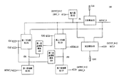
- FIG. 1 illustrates a schematic diagram of a shift register unit in accordance with one embodiment of the present disclosure
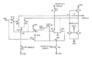
- FIG. 2 illustrates a schematic structural diagram of a shift register unit in accordance with one embodiment of the present disclosure
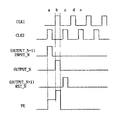
- FIG. 3 illustrates a signal timing diagram of a shift register unit in accordance with one embodiment of the present disclosure
- FIG. 4 illustrates a schematic structural diagram of a gate driving device according to an embodiment of the present disclosure.
- the transistors employed in all embodiments of the present invention may be thin film transistors or field effect transistors or other devices having the same characteristics.
- the source and drain of each transistor can be used interchangeably, so for convenience of description, one of them is referred to as a first pole and the other is referred to as a second pole.
- FIG. 1 illustrates a schematic diagram of a shift register unit in accordance with one embodiment of the present disclosure.
- the shift register unit 100 includes a pull-up module 101, an input module 102, a reset module 103, a first pull-down module 104, a second pull-down module 105, a first control module 106, and a second control module. 107.
- the pull-up module connects the first clock signal port CLK1, the pull-up control node PU, and the signal output terminal OUTPUT_N (in the Nth shift register in the cascade structure)
- the unit is taken as an example, for pulling up a signal outputted by the signal output terminal to a high level according to a potential of the pull-up control node and a first clock signal input by the first clock signal port, where the pull-up control node is Pull the connection point between the module and the input module.
- the input module is connected to the signal input terminal INPUT_N (which is usually connected to the signal output port OUTPUT_N-1 of the previous shift register unit) and the pull-up control node for controlling the potential of the pull-up control node according to the signal input from the signal input terminal.
- the reset module is connected to the reset signal terminal RST_N (which is usually connected to the signal output port OUTPUT_N+1 of the next shift register unit), the first clock signal port, the pull-up control node, and the signal output terminal for input according to the reset signal terminal
- the signal and the first clock signal input by the first clock signal port pull the potential of the pull-up control node and the signal outputted by the signal output to a low level.
- the first pull-down module is connected to the first clock signal port, the second clock signal port CLK2 inputting the second clock signal, the first control node CN1, the pull-up control node, and the signal output terminal, and the potential of the first clock signal is high.
- the potential of the second clock signal is low, the potential of the pull-up control node and the signal outputted by the signal output terminal are pulled down to a low level, and the first control node is a connection point between the first pull-down module and the first control module.
- the second pull-down module is connected to the first clock signal port, the second clock signal port, the second control node CN2, the pull-up control node, and the signal output terminal, wherein the potential of the first clock signal is low and the potential of the second clock signal is high
- the potential of the pull-up control node and the signal outputted by the signal output terminal are pulled down to a low level
- the second control node is a connection point of the second pull-down module and the second control module.
- the first control module is connected to the signal output end and the first control node, and is configured to disable the first pull-down module when the signal output end outputs a signal.
- the second control module is connected to the signal input end and the second control node for deactivating the second pull-down module when the signal input signal is input.
- the first state clearing module is coupled to the second clock signal port and the first control node for clearing the state of the first pulldown module when the second clock signal potential is high.
- the second state clearing module is coupled to the first clock signal port and the second control node for clearing the state of the second pulldown module when the first clock signal potential is high.
- FIG. 2 illustrates a schematic structural diagram of a shift register unit according to an embodiment of the present disclosure.
- the pull-up module includes: a first transistor M1 having a gate connected to the pull-up control node PU, a first pole connected to the first clock signal port CLK1, and a second pole connected to the signal output terminal OUTPUT_N;
- a capacitor C1 has one end connected to the pull-up control node PU and the other end connected to the signal output terminal OUTPUT_N.
- the input module includes a second transistor M2 having a gate and a first pole connected to the signal input terminal INPUT_N and a second pole connected to the pull-up control node PU.
- the reset module includes: a third transistor M3 having a gate connected to the reset signal terminal RST_N, a first pole connected to the first clock signal port, a second pole connected to the pull-up control node, and a fourth transistor M4 having a gate connected thereto At the reset signal end, the first pole is connected to the signal output port, and the second pole is connected to the first clock signal port.
- the first pull-down module includes: a fifth transistor M5 having a gate and a first pole connected to the first clock signal port, a second pole connected to the first control node, and a sixth transistor M6 having a gate connected to the first control Node CN1, the first pole is connected to the pull-up control node, the second pole is connected to the second clock signal port CLK2; the seventh transistor M7 has its gate connected to the first control node, and the first pole is connected to the signal output end, The two poles are connected to the second clock signal port.
- the second pull-down module includes: an eighth transistor M8 having a gate and a first pole connected to the second clock signal port, a second pole connected to the second control node CN2, and a ninth transistor M9 having a gate connected to the second control a node, the first pole is connected to the pull-up control node, the second pole is connected to the first clock signal port; the tenth transistor M10 has a gate connected to the second control node, and the first pole is connected to the first clock signal port, The two poles are connected to the signal output.
- the first control module includes an eleventh transistor M11 having a gate connected to the signal output, a first pole connected to the second clock signal port, and a second pole connected to the first control node.
- the second control module includes a twelfth transistor M12 having a gate connected to the signal reset terminal, a first pole connected to the second control node, and a second pole connected to the first clock signal port.
- the first state clearing module includes a thirteenth transistor M13 having a gate connected to the second clock signal port, a first pole connected to the first control node, and a second pole connected to the first clock signal port.
- the second state clearing module includes a fourteenth transistor M14 having a gate connected to the first clock signal port, a first pole connected to the second clock signal port, and a second pole connected to the second control node.
- FIG. 2 The circuit structure shown in FIG. 2 is described by taking a P-type transistor as an example. However, based on the description and teaching of the implementation of the P-type transistor herein, those skilled in the art can easily think of adopting N without requiring creative labor. The implementation of the transistor, all of which are covered by the scope of the present invention. Therefore, it should be noted that the structures of the various modules described above are merely exemplary and not limiting, and any structure that can implement the functions of the modules described above is contemplated.
- FIG. 3 illustrates a signal timing diagram of a shift register unit in accordance with one embodiment of the present disclosure.
- the exemplary knot of FIG. 2 is now combined. The composition is described.
- the first clock signal input by the first clock signal port CLK1 and the second clock signal input by the second clock signal port CLK2 are mutually inverted, and preferably the first clock signal and the second clock signal are occupied.
- CLK1 is low
- CLK2 is high
- signal input INPUT_N has signal input (ie, port appears high)
- reset signal RST_N has no signal input (port is low) .
- the signal input INPUT_N is usually connected to the signal output (OUTPUT_N-1) of the previous shift register unit.
- the second transistor M2 is turned on to charge the first capacitor C1, so that the potential of the PU point is controlled to a high level.
- the second control module is started (ie, M12 is turned on) to disable the second pull-down module (the CN2 point is low, thereby causing M9 and M10 to be turned off), and at the same time, due to CLK1.
- the terminal is low and the first pull-down module does not work (M5 is off).
- the CLK1 terminal has a high level
- the CLK2 terminal has a low level
- the signal input terminal has no signal input
- the reset signal terminal has no signal input.
- the first transistor M1 of the pull-up module is turned on, so that the signal output from the signal output terminal OUTPUT_N is pulled up to a high level.
- the signal output can be connected to the gate of the pixel region to provide a gate drive signal thereto. It should be noted that the potential of the PU point will continue to rise due to the coupling of the capacitors.
- the first control module is started (M11 is turned on) to disable the first pull-down module (the CN1 point is low, resulting in M6). And M7 cutoff), and because the CLK2 terminal is low, the second pull-down module does not work (M8 cutoff).
- the CLK1 terminal is low level
- the CLK2 terminal is high level
- the reset signal terminal RST_N has a signal input
- the signal output of the adjacent next shift register unit is
- the terminal (OUTPUT_N+1) has a signal output.
- M3 and M4 in the reset module are turned on, and the potentials of the PU point and the OUTPUT_N point are quickly pulled down to a low level.
- the second pull-down module is enabled (M8, M9, and M10 are turned on), ensuring that the potential of the PU point and OUTPUT_N are pulled low.
- the CLK1 terminal has a high level
- the CLK2 terminal has a low level
- the signal input terminal and the reset signal terminal have no signal input
- the signal output terminal has no level output.
- the first pull-down module is enabled (M5, M6, and M7 are turned on), and the PU point and OUTPUT_N are maintained. The potential is low.
- the second state clearing module works (M14 is turned on) to clear the previous state of the second pull-down module to avoid suspension thereof and cause instability of the circuit.
- the second pull-down module is enabled to keep the potential of the PU point and the OUTPUT_N electric low.
- the first state clearing module works (M13 is turned on) to clear the previous state of the first pull-down module to avoid suspension thereof and cause instability of the circuit.
- FIG. 4 illustrates a schematic structural diagram of a gate driving device according to an embodiment of the present disclosure.
- the gate driving device 400 includes a plurality of shift register units 100_1, ..., 100_N, each of which may have the same structure as the shift register unit of FIG.
- the plurality of shift register units are cascaded with each other, except for the first shift register unit 100_1 and the last shift register unit 100_N, the signal output ends of each of the shift register units are connected to the next adjacent one An input terminal of the shift register unit and a reset signal terminal connected to a previous shift register unit adjacent thereto.
- the signal input end of the first shift register unit inputs a frame start signal STV, and the signal output end is connected to a signal input end of the second shift register unit.
- the signal output terminal of the last shift register unit is connected to the reset signal terminal of the previous shift register unit adjacent thereto.
- the first voltage source CLK and the second voltage source CLKB shown in FIG. 4 are mutually inverted, so that the clock signals input to the first clock signal port of the adjacent two-stage shift register unit are inverted with each other, and the second clock The clock signals input to the signal port are inverted from each other.
- a display device that includes a gate driving device as described above.
Landscapes
- Engineering & Computer Science (AREA)
- Chemical & Material Sciences (AREA)
- Crystallography & Structural Chemistry (AREA)
- Physics & Mathematics (AREA)
- Computer Hardware Design (AREA)
- General Physics & Mathematics (AREA)
- Theoretical Computer Science (AREA)
- Shift Register Type Memory (AREA)
- Liquid Crystal Display Device Control (AREA)
- Control Of Indicators Other Than Cathode Ray Tubes (AREA)
Abstract
Description
Claims (13)
- 一种移位寄存器单元,包括上拉模块、输入模块、复位模块、第一下拉模块、第二下拉模块、第一控制模块、第二控制模块、第一状态清除模块和第二状态清除模块;上拉模块连接第一时钟信号端口、上拉控制节点(PU)以及信号输出端,用于根据上拉控制节点的电位和所述第一时钟信号端口输入的第一时钟信号将信号输出端输出的信号上拉为高电平,所述上拉控制节点为上拉模块与输入模块的连接点;输入模块连接信号输入端以及上拉控制节点,用于根据信号输入端输入的信号控制上拉控制节点的电位;复位模块连接复位信号端、第一时钟信号端口、上拉控制节点以及信号输出端,用于根据复位信号端输入的信号和第一时钟信号将上拉控制节点的电位和信号输出端输出的信号下拉为低电平;第一下拉模块连接第一时钟信号端口、输入第二时钟信号的第二时钟信号端口、第一控制节点、上拉控制节点以及信号输出端,用于在第一时钟信号电位为高且第二时钟信号电位为低时将上拉控制节点的电位和信号输出端输出的信号下拉为低电平,第一控制节点为第一下拉模块与第一控制模块的连接点;第二下拉模块连接第一时钟信号端口、第二时钟信号端口、第二控制节点、上拉控制节点以及信号输出端,用于在第一时钟信号电位为低且第二时钟信号电位为高时将上拉控制节点的电位和信号输出端输出的信号下拉为低电平,第二控制节点为第二下拉模块与第二控制模块的连接点;第一控制模块连接信号输出端和第一控制节点,用于在信号输出端输出信号时停用第一下拉模块;第二控制模块连接信号输入端和第二控制节点,用于在信号输入端输入信号时停用第二下拉模块;第一状态清除模块连接第二时钟信号端口和第一控制节点,用于在第二时钟信号电位为高时清除第一下拉模块的状态;第二状态清除模块连接第一时钟信号端口和第二控制节点,用于在第一时钟信号电位为高时清除第二下拉模块的状态。
- 根据权利要求1的移位寄存器单元,所述上拉模块包括:第一晶体管,其栅极连接到上拉控制节点,第一极连接到第一时钟信号端口,第二极连接到信号输出端;第一电容,其一端连接到上拉控制节点,另一端连接到信号输出端。
- 根据权利要求1的移位寄存器单元,所述输入模块包括:第二晶体管,其栅极和第一极连接到信号输入端,第二极连接到上拉控制节点。
- 根据权利要求1的移位寄存器单元,所述复位模块包括:第三晶体管,其栅极连接到复位信号端,第一极连接到第一时钟信号端口,第二极连接到上拉控制节点;第四晶体管,其栅极连接到复位信号端,第一极连接到信号输出端口节点,第二极连接到第一时钟信号端口。
- 根据权利要求1的移位寄存器单元,所述第一下拉模块包括:第五晶体管,其栅极和第一极连接到第一时钟信号端口,第二极连接到第一控制节点;第六晶体管,其栅极连接到第一控制节点,第一极连接到上拉控制节点,第二极连接到第二时钟信号端口;第七晶体管,其栅极连接到第一控制节点,第一极连接到信号输出端,第二极连接到第二时钟信号端口。
- 根据权利要求1的移位寄存器单元,所述第二下拉模块包括:第八晶体管,其栅极和第一极连接到第二时钟信号端口,第二极连接到第二控制节点;第九晶体管,其栅极连接到第二控制节点,第一极连接到上拉控制节点,第二极连接到第一时钟信号端口;第十晶体管,其栅极连接到第二控制节点,第一极连接到第一时钟信号端口,第二极连接到信号输出端。
- 根据权利要求1的移位寄存器单元,所述第一控制模块包括:第十一晶体管,其栅极连接到信号输出端,第一极连接到第二时钟信号端口,第二极连接到第一控制节点。
- 根据权利要求1的移位寄存器单元,所述第二控制模块包括:第十二晶体管,其栅极连接到信号复位端,第一极连接到第二控 制节点,第二极连接到第一时钟信号端口。
- 根据权利要求1的移位寄存器单元,所述第一状态清除模块包括:第十三晶体管,其栅极连接到第二时钟信号端口,第一极连接到第一控制节点,第二极连接到第一时钟信号端口。
- 根据权利要求1的移位寄存器单元,所述第二状态清除模块包括:第十四晶体管,其栅极连接到第一时钟信号端口,第一极连接到第二时钟信号端口,第二极连接到第二控制节点。
- 一种栅极驱动装置,包括多个根据权利要求1-10中任意一项所述的移位寄存器单元,其中所述多个移位寄存器单元相互级联,除第一个移位寄存器单元和最后一个移位寄存器单元外,其余每个移位寄存器单元的信号输出端都连接与其相邻的下一个移位寄存器单元的输入端以及连接与其相邻的上一个移位寄存器单元的复位信号端;其中所述第一个移位寄存器单元的信号输入端输入帧起始信号,信号输出端与第二个移位寄存器单元的信号输入端连接,所述最后一个移位寄存器单元的信号输出端连接与其相邻的上一个移位寄存器单元的复位信号端。
- 根据权利要求11所述的栅极驱动装置,其中相邻两级移位寄存器单元的第一时钟信号端口输入的时钟信号互为反相,第二时钟信号端口输入的时钟信号互为反相。
- 一种显示装置,其包括如权利要求11-12中任意一项所述的栅极驱动装置。
Priority Applications (1)
| Application Number | Priority Date | Filing Date | Title |
|---|---|---|---|
| US14/913,318 US9792868B2 (en) | 2015-04-09 | 2015-08-03 | Shift register unit, gate driving device and display device |
Applications Claiming Priority (2)
| Application Number | Priority Date | Filing Date | Title |
|---|---|---|---|
| CN201510165136.2A CN104700769B (zh) | 2015-04-09 | 2015-04-09 | 移位寄存器单元、栅极驱动装置以及显示装置 |
| CN201510165136.2 | 2015-04-09 |
Publications (1)
| Publication Number | Publication Date |
|---|---|
| WO2016161725A1 true WO2016161725A1 (zh) | 2016-10-13 |
Family
ID=53347836
Family Applications (1)
| Application Number | Title | Priority Date | Filing Date |
|---|---|---|---|
| PCT/CN2015/085941 Ceased WO2016161725A1 (zh) | 2015-04-09 | 2015-08-03 | 移位寄存器单元、栅极驱动装置以及显示装置 |
Country Status (3)
| Country | Link |
|---|---|
| US (1) | US9792868B2 (zh) |
| CN (1) | CN104700769B (zh) |
| WO (1) | WO2016161725A1 (zh) |
Families Citing this family (12)
| Publication number | Priority date | Publication date | Assignee | Title |
|---|---|---|---|---|
| CN104700769B (zh) * | 2015-04-09 | 2017-03-15 | 京东方科技集团股份有限公司 | 移位寄存器单元、栅极驱动装置以及显示装置 |
| CN105161134B (zh) * | 2015-10-09 | 2018-10-23 | 京东方科技集团股份有限公司 | 移位寄存器单元及其操作方法、移位寄存器 |
| CN105206240B (zh) * | 2015-10-22 | 2018-07-13 | 武汉华星光电技术有限公司 | In Cell型触控显示面板的驱动方法 |
| CN105185349B (zh) * | 2015-11-04 | 2018-09-11 | 京东方科技集团股份有限公司 | 一种移位寄存器、栅极集成驱动电路及显示装置 |
| CN105845183B (zh) * | 2016-03-21 | 2019-08-13 | 京东方科技集团股份有限公司 | 移位寄存器电路、阵列基板和显示装置 |
| CN105702297B (zh) | 2016-04-15 | 2019-12-31 | 京东方科技集团股份有限公司 | 移位寄存器及驱动方法、驱动电路、阵列基板及显示装置 |
| CN106328080B (zh) * | 2016-09-27 | 2019-02-19 | 南京中电熊猫液晶显示科技有限公司 | 一种goa电路控制的方法 |
| CN107633831B (zh) * | 2017-10-18 | 2020-02-14 | 京东方科技集团股份有限公司 | 移位寄存器及其驱动方法、栅极驱动电路和显示装置 |
| CN111223459B (zh) | 2018-11-27 | 2022-03-08 | 元太科技工业股份有限公司 | 移位寄存器以及栅极驱动电路 |
| CN112447141B (zh) * | 2019-08-30 | 2022-04-08 | 京东方科技集团股份有限公司 | 移位寄存器及其驱动方法、栅极驱动电路、显示面板 |
| KR102782272B1 (ko) * | 2020-10-23 | 2025-03-17 | 엘지디스플레이 주식회사 | 표시장치 및 이의 구동방법 |
| CN114937471A (zh) * | 2022-05-27 | 2022-08-23 | 京东方科技集团股份有限公司 | 移位寄存器及其驱动电路、方法、显示面板、装置 |
Citations (5)
| Publication number | Priority date | Publication date | Assignee | Title |
|---|---|---|---|---|
| EP1160796A2 (en) * | 2000-05-31 | 2001-12-05 | Casio Computer Co., Ltd. | Shift register and electronic apparatus |
| US20070242000A1 (en) * | 2006-04-18 | 2007-10-18 | Dong Yong Shin | Scan driving circuit and organic light emitting display using the same |
| CN102629459A (zh) * | 2011-10-26 | 2012-08-08 | 北京京东方光电科技有限公司 | 栅线驱动方法、移位寄存器及栅线驱动装置 |
| CN102654986A (zh) * | 2011-11-25 | 2012-09-05 | 京东方科技集团股份有限公司 | 移位寄存器的级、栅极驱动器、阵列基板以及显示装置 |
| CN104700769A (zh) * | 2015-04-09 | 2015-06-10 | 京东方科技集团股份有限公司 | 移位寄存器单元、栅极驱动装置以及显示装置 |
Family Cites Families (21)
| Publication number | Priority date | Publication date | Assignee | Title |
|---|---|---|---|---|
| KR101127842B1 (ko) * | 2005-06-13 | 2012-03-21 | 엘지디스플레이 주식회사 | 쉬프트 레지스터와 이를 이용한 액정표시장치 |
| CN101335050B (zh) * | 2007-06-26 | 2011-02-09 | 上海天马微电子有限公司 | 移位寄存器及使用该移位寄存器的液晶显示器 |
| CN101826310A (zh) * | 2009-03-06 | 2010-09-08 | 华映视讯(吴江)有限公司 | 高可靠度栅极驱动电路 |
| JP5669453B2 (ja) * | 2010-06-22 | 2015-02-12 | 株式会社ジャパンディスプレイ | 双方向シフトレジスタ、及びこれを用いた画像表示装置 |
| JP5485811B2 (ja) * | 2010-06-23 | 2014-05-07 | 株式会社ジャパンディスプレイ | 双方向シフトレジスタ、及びこれを用いた画像表示装置 |
| TWI440308B (zh) * | 2010-10-13 | 2014-06-01 | Au Optronics Corp | 閘極陣列移位暫存器 |
| CN202502720U (zh) * | 2012-03-16 | 2012-10-24 | 合肥京东方光电科技有限公司 | 一种移位寄存器、阵列基板栅极驱动装置和显示装置 |
| CN103021354B (zh) * | 2012-11-21 | 2015-07-15 | 京东方科技集团股份有限公司 | 移位寄存器单元、栅极驱动电路及显示装置 |
| CN103050106B (zh) * | 2012-12-26 | 2015-02-11 | 京东方科技集团股份有限公司 | 栅极驱动电路、显示模组和显示器 |
| CN103165190A (zh) * | 2013-02-01 | 2013-06-19 | 京东方科技集团股份有限公司 | 移位寄存器单元、移位寄存器、阵列基板和显示装置 |
| CN103226979B (zh) * | 2013-02-18 | 2016-03-09 | 合肥京东方光电科技有限公司 | 一种双向移位寄存器单元、双向移位寄存器及显示装置 |
| CN103258494B (zh) * | 2013-04-16 | 2015-10-14 | 合肥京东方光电科技有限公司 | 一种移位寄存器、栅极驱动装置和液晶显示装置 |
| CN103280200B (zh) * | 2013-04-22 | 2015-01-21 | 京东方科技集团股份有限公司 | 移位寄存器单元、栅极驱动电路与显示器件 |
| CN103366704B (zh) * | 2013-07-10 | 2015-08-19 | 京东方科技集团股份有限公司 | 一种移位寄存器单元及栅极驱动电路、显示装置 |
| CN103489484B (zh) * | 2013-09-22 | 2015-03-25 | 京东方科技集团股份有限公司 | 一种移位寄存器单元及栅极驱动电路 |
| CN104252853A (zh) * | 2014-09-04 | 2014-12-31 | 京东方科技集团股份有限公司 | 移位寄存器单元及驱动方法、栅极驱动电路及显示器件 |
| CN104332146B (zh) * | 2014-11-12 | 2016-09-28 | 合肥鑫晟光电科技有限公司 | 移位寄存器单元、移位寄存器、栅极驱动电路和显示装置 |
| CN104361852A (zh) * | 2014-11-28 | 2015-02-18 | 上海中航光电子有限公司 | 移位寄存器、栅极驱动电路及显示装置 |
| CN104616616B (zh) * | 2015-02-12 | 2017-12-15 | 京东方科技集团股份有限公司 | 栅极驱动电路及其驱动方法、阵列基板、显示装置 |
| CN104637462A (zh) * | 2015-03-17 | 2015-05-20 | 合肥京东方光电科技有限公司 | 移位寄存器单元及其驱动方法、栅极驱动电路、显示装置 |
| CN104732939A (zh) * | 2015-03-27 | 2015-06-24 | 京东方科技集团股份有限公司 | 移位寄存器、栅极驱动电路、显示装置及栅极驱动方法 |
-
2015
- 2015-04-09 CN CN201510165136.2A patent/CN104700769B/zh not_active Expired - Fee Related
- 2015-08-03 WO PCT/CN2015/085941 patent/WO2016161725A1/zh not_active Ceased
- 2015-08-03 US US14/913,318 patent/US9792868B2/en not_active Expired - Fee Related
Patent Citations (5)
| Publication number | Priority date | Publication date | Assignee | Title |
|---|---|---|---|---|
| EP1160796A2 (en) * | 2000-05-31 | 2001-12-05 | Casio Computer Co., Ltd. | Shift register and electronic apparatus |
| US20070242000A1 (en) * | 2006-04-18 | 2007-10-18 | Dong Yong Shin | Scan driving circuit and organic light emitting display using the same |
| CN102629459A (zh) * | 2011-10-26 | 2012-08-08 | 北京京东方光电科技有限公司 | 栅线驱动方法、移位寄存器及栅线驱动装置 |
| CN102654986A (zh) * | 2011-11-25 | 2012-09-05 | 京东方科技集团股份有限公司 | 移位寄存器的级、栅极驱动器、阵列基板以及显示装置 |
| CN104700769A (zh) * | 2015-04-09 | 2015-06-10 | 京东方科技集团股份有限公司 | 移位寄存器单元、栅极驱动装置以及显示装置 |
Also Published As
| Publication number | Publication date |
|---|---|
| US20170039969A1 (en) | 2017-02-09 |
| CN104700769A (zh) | 2015-06-10 |
| US9792868B2 (en) | 2017-10-17 |
| CN104700769B (zh) | 2017-03-15 |
Similar Documents
| Publication | Publication Date | Title |
|---|---|---|
| WO2016161725A1 (zh) | 移位寄存器单元、栅极驱动装置以及显示装置 | |
| CN104700814B (zh) | 移位寄存器单元、栅极驱动装置以及显示装置 | |
| US9478310B2 (en) | Shift register unit, gate driving circuit and method, display apparatus | |
| CN104766586B (zh) | 移位寄存器单元、其驱动方法、栅极驱动电路及显示装置 | |
| CN104157252B (zh) | 一种移位寄存器、栅极驱动电路及显示装置 | |
| CN105304011B (zh) | 移位寄存器单元及其驱动方法、栅极驱动电路和显示装置 | |
| JP6423957B2 (ja) | Igzo製造工程に基づくゲート電極駆動回路 | |
| CN107799087B (zh) | 一种goa电路及显示装置 | |
| US9691312B2 (en) | Shift register unit, shift register and display apparatus | |
| CN103400561B (zh) | 栅极驱动电路 | |
| JP2019537044A (ja) | 走査駆動回路および表示装置 | |
| WO2017054399A1 (zh) | 一种移位寄存器, 其驱动方法, 栅极驱动电路及显示装置 | |
| WO2017211094A1 (zh) | 一种移位寄存器、栅极驱动电路及显示装置 | |
| CN103021466A (zh) | 移位寄存器及其工作方法、栅极驱动装置、显示装置 | |
| CN105427825A (zh) | 一种移位寄存器、其驱动方法及栅极驱动电路 | |
| CN104934071B (zh) | 一种移位寄存器、栅极驱动电路及显示装置 | |
| WO2016141652A1 (zh) | 移位寄存器单元、移位寄存器、显示面板及显示装置 | |
| CN110782940B (zh) | 移位寄存单元、栅极驱动电路、阵列基板及显示装置 | |
| JP2019501409A (ja) | 液晶表示装置及びgoa回路 | |
| JP2018536192A (ja) | 液晶表示装置及びgoa回路 | |
| CN109427409B (zh) | 移位寄存器、栅极驱动电路、显示面板及驱动方法 | |
| CN206040190U (zh) | 移位寄存器单元及栅极驱动电路、显示装置 | |
| US10438554B2 (en) | Shift register and driving method thereof, gate on array circuit and display apparatus | |
| CN104867435B (zh) | 移位暂存器及移位暂存电路 | |
| CN107393499B (zh) | 一种方波削角电路、其驱动方法及显示面板 |
Legal Events
| Date | Code | Title | Description |
|---|---|---|---|
| WWE | Wipo information: entry into national phase |
Ref document number: 14913318 Country of ref document: US |
|
| 121 | Ep: the epo has been informed by wipo that ep was designated in this application |
Ref document number: 15888280 Country of ref document: EP Kind code of ref document: A1 |
|
| NENP | Non-entry into the national phase |
Ref country code: DE |
|
| 122 | Ep: pct application non-entry in european phase |
Ref document number: 15888280 Country of ref document: EP Kind code of ref document: A1 |
|
| 122 | Ep: pct application non-entry in european phase |
Ref document number: 15888280 Country of ref document: EP Kind code of ref document: A1 |
|
| 32PN | Ep: public notification in the ep bulletin as address of the adressee cannot be established |
Free format text: NOTING OF LOSS OF RIGHTS PURSUANT TO RULE 112(1) EPC (EPO FORM 1205 DATED 12/04/2018) |
|
| 122 | Ep: pct application non-entry in european phase |
Ref document number: 15888280 Country of ref document: EP Kind code of ref document: A1 |