WO2016117424A1 - シャフト端部取付構造 - Google Patents
シャフト端部取付構造 Download PDFInfo
- Publication number
- WO2016117424A1 WO2016117424A1 PCT/JP2016/050796 JP2016050796W WO2016117424A1 WO 2016117424 A1 WO2016117424 A1 WO 2016117424A1 JP 2016050796 W JP2016050796 W JP 2016050796W WO 2016117424 A1 WO2016117424 A1 WO 2016117424A1
- Authority
- WO
- WIPO (PCT)
- Prior art keywords
- shaft
- bottom plate
- ring member
- mounting structure
- ceramic
- Prior art date
- Legal status (The legal status is an assumption and is not a legal conclusion. Google has not performed a legal analysis and makes no representation as to the accuracy of the status listed.)
- Ceased
Links
Images

Classifications
-
- H—ELECTRICITY
- H10—SEMICONDUCTOR DEVICES; ELECTRIC SOLID-STATE DEVICES NOT OTHERWISE PROVIDED FOR
- H10P—GENERIC PROCESSES OR APPARATUS FOR THE MANUFACTURE OR TREATMENT OF DEVICES COVERED BY CLASS H10
- H10P72/00—Handling or holding of wafers, substrates or devices during manufacture or treatment thereof
- H10P72/70—Handling or holding of wafers, substrates or devices during manufacture or treatment thereof for supporting or gripping
-
- H—ELECTRICITY
- H10—SEMICONDUCTOR DEVICES; ELECTRIC SOLID-STATE DEVICES NOT OTHERWISE PROVIDED FOR
- H10P—GENERIC PROCESSES OR APPARATUS FOR THE MANUFACTURE OR TREATMENT OF DEVICES COVERED BY CLASS H10
- H10P72/00—Handling or holding of wafers, substrates or devices during manufacture or treatment thereof
- H10P72/70—Handling or holding of wafers, substrates or devices during manufacture or treatment thereof for supporting or gripping
- H10P72/76—Handling or holding of wafers, substrates or devices during manufacture or treatment thereof for supporting or gripping using mechanical means, e.g. clamps or pinches
- H10P72/7604—Handling or holding of wafers, substrates or devices during manufacture or treatment thereof for supporting or gripping using mechanical means, e.g. clamps or pinches the wafers being placed on a susceptor, stage or support
- H10P72/7626—Handling or holding of wafers, substrates or devices during manufacture or treatment thereof for supporting or gripping using mechanical means, e.g. clamps or pinches the wafers being placed on a susceptor, stage or support characterised by the construction of the shaft
-
- H—ELECTRICITY
- H10—SEMICONDUCTOR DEVICES; ELECTRIC SOLID-STATE DEVICES NOT OTHERWISE PROVIDED FOR
- H10P—GENERIC PROCESSES OR APPARATUS FOR THE MANUFACTURE OR TREATMENT OF DEVICES COVERED BY CLASS H10
- H10P72/00—Handling or holding of wafers, substrates or devices during manufacture or treatment thereof
- H10P72/04—Apparatus for manufacture or treatment
- H10P72/0431—Apparatus for thermal treatment
- H10P72/0432—Apparatus for thermal treatment mainly by conduction
-
- H—ELECTRICITY
- H10—SEMICONDUCTOR DEVICES; ELECTRIC SOLID-STATE DEVICES NOT OTHERWISE PROVIDED FOR
- H10P—GENERIC PROCESSES OR APPARATUS FOR THE MANUFACTURE OR TREATMENT OF DEVICES COVERED BY CLASS H10
- H10P72/00—Handling or holding of wafers, substrates or devices during manufacture or treatment thereof
- H10P72/04—Apparatus for manufacture or treatment
- H10P72/0441—Apparatus for sealing, encapsulating, glassing, decapsulating or the like
-
- H—ELECTRICITY
- H10—SEMICONDUCTOR DEVICES; ELECTRIC SOLID-STATE DEVICES NOT OTHERWISE PROVIDED FOR
- H10P—GENERIC PROCESSES OR APPARATUS FOR THE MANUFACTURE OR TREATMENT OF DEVICES COVERED BY CLASS H10
- H10P72/00—Handling or holding of wafers, substrates or devices during manufacture or treatment thereof
- H10P72/70—Handling or holding of wafers, substrates or devices during manufacture or treatment thereof for supporting or gripping
- H10P72/72—Handling or holding of wafers, substrates or devices during manufacture or treatment thereof for supporting or gripping using electrostatic chucks
-
- H—ELECTRICITY
- H10—SEMICONDUCTOR DEVICES; ELECTRIC SOLID-STATE DEVICES NOT OTHERWISE PROVIDED FOR
- H10P—GENERIC PROCESSES OR APPARATUS FOR THE MANUFACTURE OR TREATMENT OF DEVICES COVERED BY CLASS H10
- H10P72/00—Handling or holding of wafers, substrates or devices during manufacture or treatment thereof
- H10P72/70—Handling or holding of wafers, substrates or devices during manufacture or treatment thereof for supporting or gripping
- H10P72/76—Handling or holding of wafers, substrates or devices during manufacture or treatment thereof for supporting or gripping using mechanical means, e.g. clamps or pinches
- H10P72/7604—Handling or holding of wafers, substrates or devices during manufacture or treatment thereof for supporting or gripping using mechanical means, e.g. clamps or pinches the wafers being placed on a susceptor, stage or support
- H10P72/7616—Handling or holding of wafers, substrates or devices during manufacture or treatment thereof for supporting or gripping using mechanical means, e.g. clamps or pinches the wafers being placed on a susceptor, stage or support characterised by a coating, a hardness or a material
Definitions
- the present invention relates to a shaft end mounting structure.
- Patent Document 1 A member for a semiconductor manufacturing apparatus in which a ceramic plate on which a wafer is placed and a hollow ceramic shaft are integrated is known (for example, Patent Document 1).
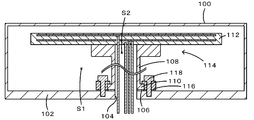
- a shaft end mounting structure shown in FIG. 4 is known as a shaft end mounting structure in which the end of a hollow ceramic shaft of such a semiconductor manufacturing apparatus member is hermetically attached to the periphery of a through hole provided in the bottom plate of the chamber.
- the flange 110 of the hollow ceramic shaft 108 is placed on the periphery of the through hole 104 provided in the bottom plate 102 of the chamber 100 via the ring-shaped metal seal 106.
- the hollow ceramic shaft 108 is integrated with the ceramic plate 112 to constitute a ceramic heater 114.
- a clamp 116 in which two half-rings having an inverted L-shaped cross section are combined to form a ring shape presses the flange 110 of the hollow ceramic shaft 108 from above.
- the bolt 118 passes through the clamp 116 from the upper surface of the clamp 116 and is screwed to the bottom plate 102 of the chamber 100.
- the internal space S1 of the chamber 100 and the internal space S2 of the hollow ceramic shaft 108 are hermetically separated. Therefore, the internal space S1 of the chamber 100 can be made into a vacuum atmosphere, and the internal space S1 and the internal space S2 of the hollow ceramic shaft 108 can be cut off.
- the flange 110 of the hollow ceramic shaft 108 is sandwiched between the clamp 116 and the bottom plate 102 of the chamber 100. Therefore, if the bolt 118 is tightened too much, the hollow ceramic shaft 108 will break. There was a fear. On the other hand, if it is attempted to avoid cracking of the hollow ceramic shaft 108, the bolt 118 may be loosely tightened, the metal seal 106 may not function sufficiently, and the internal space S1 of the chamber 100 and the internal space S2 of the hollow ceramic shaft 108 There was a problem that could not be separated in an airtight manner.
- the present invention has been made in view of the above-described problems, and has as its main object to sufficiently separate the internal space of the chamber and the internal space of the hollow ceramic shaft without damaging the hollow ceramic shaft.
- the shaft end mounting structure of the present invention is A shaft end mounting structure in which an end of a hollow ceramic shaft integrated with a ceramic plate on which a wafer is placed is hermetically attached to a periphery of a through hole provided in a bottom plate of a chamber, A ring member made of a metal material or a metal-ceramic composite material hermetically bonded to the end face of the hollow ceramic shaft via a metal layer; A fastening member that penetrates through the bottom plate and the sealing layer in a state where the ring member is placed on a peripheral edge of a through-hole provided in the bottom plate of the chamber via a seal layer, and fastens the ring member to the bottom plate; , It is equipped with.
- the hollow ceramic shaft is airtightly joined to the chamber via a ring member and a metal layer.
- the ring member is placed on the periphery of a through hole provided in the bottom plate of the chamber via the seal layer, and the fastening member is fastened so as to penetrate the bottom plate and the seal layer and attract the ring member to the bottom plate.
- the ring member is made of a metal material or a metal-ceramic composite material, and has a higher strength than ceramic. For this reason, when the fastening member is strongly tightened, the ring member is attracted to the upper surface of the bottom plate of the chamber through the seal layer, but there is no fear of damaging the ring member, and the hollow ceramic shaft is not fastened.
- the fastening member is tightened strongly, there is no possibility of damaging the hollow ceramic shaft. Further, since the fastening member can be tightened strongly, the metal seal can be sufficiently sealed. Therefore, the internal space of the chamber and the internal space of the hollow ceramic shaft can be separated sufficiently airtight.
- the fastening member may be a bolt that penetrates the bottom plate and the seal layer from the lower surface of the bottom plate and is screwed into a bolt hole of the ring member.
- the hollow ceramic shaft is made of AlN, and the ring member is made of Mo, W, or FeNiCo alloy (for example, Kovar (registered trademark)). .
- the thermal expansion coefficient of the ring member becomes close to the thermal expansion coefficient of the ceramic, so that even if heating / cooling is repeated, it is possible to prevent the joint failure between the ring member and the hollow ceramic shaft due to the thermal expansion difference. be able to.
- the metal layer is preferably an Al layer or an Al alloy layer (for example, an Al—Si—Mg alloy layer or an Al—Mg alloy layer).
- TCB Thermal-compression-bonding
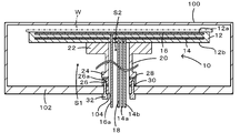
- Sectional drawing which shows an example of the shaft end part attachment structure of this invention.
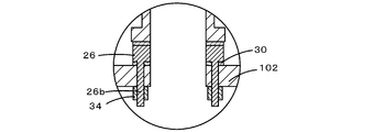
- Sectional drawing which shows another example of the shaft end part attachment structure of this invention.
- Explanatory drawing which shows the method of measuring the amount of He leak from a shaft edge part.
- Sectional drawing which shows an example of the conventional shaft edge part attachment structure.
- FIG. 1 is a cross-sectional view showing an example of a shaft end mounting structure according to the present invention. Specifically, FIG. 1 is a cross-sectional view of a ceramic heater 10 mounted inside a chamber 100.
- the ceramic heater 10 is used to heat the wafer W, and is attached inside the chamber 100 for semiconductor process.
- This ceramic heater 10 is a hollow ceramic bonded to a ceramic plate 12 having a wafer mounting surface 12a on which a wafer W can be mounted, and a surface (back surface) 12b opposite to the wafer mounting surface 12a of the ceramic plate 12.
- a shaft 20 is used to drive the wafer W, and is attached inside the chamber 100 for semiconductor process.
- This ceramic heater 10 is a hollow ceramic bonded to a ceramic plate 12 having a wafer mounting surface 12a on which a wafer W can be mounted, and a surface (back surface) 12b opposite to the wafer mounting surface 12a of the ceramic plate 12.
- a shaft 20 is used to heat the wafer W, and is attached inside the chamber 100 for semiconductor process.
- the ceramic plate 12 is a disk-shaped member whose main component is AlN.
- a heater electrode 14 and an RF electrode 16 are embedded in the ceramic plate 12.
- the heater electrode 14 is formed by wiring a coil containing Mo as a main component over the entire surface of the ceramic plate 12 in a one-stroke manner.
- One end of the heater electrode 14 is connected to a positive pole heater terminal bar 14a, and the other end is connected to a negative pole heater terminal bar 14b.
- the RF electrode 16 is a disc-shaped thin layer electrode having a diameter slightly smaller than that of the ceramic plate 12 and is formed of a mesh in which fine metal wires mainly composed of Mo are knitted into a net shape to form a sheet.
- the RF electrode 16 is embedded in the ceramic plate 12 between the heater electrode 14 and the wafer mounting surface 12a.
- An RF terminal rod 16 a is connected to the approximate center of the RF electrode 16.
- the hollow ceramic shaft 20 is a cylindrical member made of AlN, and has a first flange 22 around the upper opening and a second flange 24 around the lower opening.
- the end surface of the first flange 22 is joined to the back surface 12b of the ceramic plate 12 by TCB.
- the end face of the second flange 24 is joined to the Mo ring member 26 by TCB.
- TCB refers to a method in which a metal bonding material is sandwiched between two members to be bonded, and the two members are pressure bonded while heated to a temperature equal to or lower than the solidus temperature of the metal bonding material.
- the metal bonding material examples include an Al alloy bonding material containing Al and Mg, such as an Al—Si—Mg bonding material and an Al—Mg bonding material.
- the Al—Si—Mg-based bonding material contains 88.5% by mass of Al, 10% by mass of Si, 1.5% by mass of Mg, has a solid phase temperature of about 560 ° C., and a liquid phase temperature of about
- the TCB is heated to a temperature below the solid phase temperature (for example, about 520 to 550 ° C.) at a pressure of 20 to 140 kg / mm 2 , preferably 30 to 60 kg / mm 2 for 3 to 6 hours. Performed under pressure.
- a metal layer 28 derived from the metal bonding material used in the TCB is formed between the end surface of the second flange 24 and the ring member 26. Since the metal layer 28 is formed of TCB, pinholes are hardly generated and the airtightness is excellent. A similar metal layer (not shown) is also formed between the end face of the first flange 22 and the ceramic plate 12. A metal seal 30 (seal layer) is disposed between the ring member 26 and the periphery of the through hole 104 provided in the bottom plate 102 of the chamber 100.
- the bolt 32 (fastening member) passes through the bottom plate 102 and the metal seal 30 from the lower surface of the bottom plate 102 and is screwed into a screw hole 26 a provided on the lower surface of the ring member 26.
- Three or more (preferably six or more) bolts 32 are used at equal intervals along the circumferential direction of the ring member 26. Note that a washer may be used when the bolt 32 is fitted from the lower surface of the bottom plate 102.
- the heater terminal rods 14a and 14b and the RF terminal rod 16a described above are inserted into the internal space S2 of the hollow ceramic shaft 20, and a sheath thermocouple 18 for measuring the temperature of the ceramic plate 12 is also inserted.
- the wafer W is mounted on the wafer mounting surface 12a of the ceramic heater 10, and the internal space S1 of the chamber 100 is set to a predetermined atmosphere (for example, a hydrogen atmosphere, an argon atmosphere, or a vacuum atmosphere).
- a predetermined atmosphere for example, a hydrogen atmosphere, an argon atmosphere, or a vacuum atmosphere.
- the internal space S1 is cut off from the internal space S2 of the hollow ceramic shaft 20.
- a process for example, wafer annealing
- an AC high voltage is applied to the RF electrode 16 via the RF terminal rod 16a, so that a counter horizontal electrode (not shown) installed above the chamber 100 and an RF electrode embedded in the ceramic heater 10 are embedded. It is also possible to generate plasma between the parallel plate electrodes 16 and to use the plasma.
- an electrostatic force can be generated by applying a DC high voltage to the RF electrode 16, thereby attracting the wafer W to the wafer mounting surface 12 a.
- the temperature of the wafer W is obtained based on the detection signal of the sheath thermocouple 18, and the magnitude and on / off of the voltage applied between the two heater terminal rods 14a and 14b are controlled so that the temperature becomes the set temperature. .
- the hollow ceramic shaft 20 is airtightly joined via the ring member 26 and the metal layer 28.
- the ring member 26 is placed on the periphery of the through hole 104 provided in the bottom plate 102 of the chamber 100 through the metal seal 30, and the bolt 32 penetrates the bottom plate 102 and the metal seal 30 from the lower surface of the bottom plate 102. Are screwed together.
- the ring member 26 is made of Mo, that is, made of a metal material, and has higher strength than ceramic.
- the ring member 26 is made of Mo and has a thermal expansion coefficient close to that of AlN ceramic. Therefore, even if heating / cooling is repeated, it is possible to prevent the joint failure between the ring member 26 and the hollow ceramic shaft 20 due to the difference in thermal expansion.
- the thermal expansion coefficients of typical ceramics and metals are shown in Table 1.
- the metal layer 28 is an aluminum alloy layer
- TCB can be employed as described above. Therefore, pinholes are hardly formed in the metal layer 28, and the sealing performance of the metal layer 28 is improved.
- Mo is used as the material of the ring member 26, but W or FeNiCo alloy (for example, Kovar (registered trademark)) may be used. Since the thermal expansion coefficient of these metals is within ⁇ 20% of the thermal expansion coefficient of the AlN ceramic used in this embodiment as shown in Table 1, even if heating and cooling are repeated, the ring is caused by the difference in thermal expansion. It is possible to prevent the joint breakage between the member 26 and the hollow ceramic shaft 20 from occurring.
- AlN is used as the material of the ceramic plate 12 and the hollow ceramic shaft 20, but other ceramics may be used.
- Al 2 O 3 it is preferable to use CuW (11% Cu-89% W, see Table 1) having a close thermal expansion coefficient as the material of the ring member 26.
- the metal seal 30 is used as the seal layer, but an O-ring may be used instead of the metal seal 30. In this case, an O-ring that can withstand the operating temperature of the ceramic heater 10 is used.
- the metal layer 28 is formed by TCB, but may be formed by brazing.
- TCB Various conventionally known brazing materials can be used as the brazing material.
- TCB is preferred because pinholes are less likely to occur in the metal layer 28 than brazing.
- the bolt 32 is used as the fastening member, but the structure shown in FIG. That is, a plurality of bolt feet 26b are provided on the lower surface of the ring member 26, the bolt feet 26b penetrate the metal seal 30 and the bottom plate 102 and protrude from the lower surface of the bottom plate 102, and a nut 34 is fitted on the bolt foot 26b.
- the ring member 26 may be fastened so as to be attracted to the bottom plate 26. Even if it does in this way, the effect similar to embodiment mentioned above is acquired.
- a washer may be used when fitting the nut 34 to the bolt foot 26b.
- the amount of He leak from the shaft end was evaluated when the shaft end mounting structure of the above-described embodiment (FIG. 1) was employed and when the conventional shaft end mounting structure of FIG. 4 was employed.
- a He leak detector 120 was attached to the port of the chamber 100, the degree of vacuum in the chamber was set to 5E-2 [Pa], and the temperature at the end of the shaft was set to RT (room temperature).
- RT room temperature
- He gas was blown into the internal space S2 of the hollow ceramic shaft 20, the numerical value of the He leak detector 120 was read, and the numerical value was taken as the amount of He leak at RT.
- the temperature at the end of the shaft was set to 100 ° C.
- the numerical value of the He leak detector 120 was read in the same manner, and the numerical value was taken as the amount of He leak at 100 ° C.
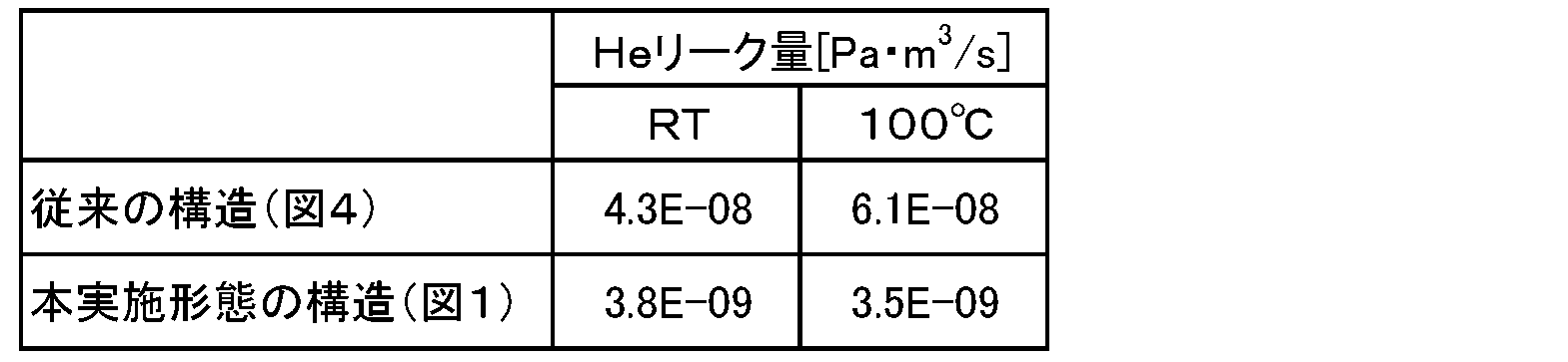
- the amount of He leakage was measured in the same manner. The results are shown in Table 2. As shown in Table 2, when the shaft end mounting structure of FIG. 1 was adopted, the amount of He leak was reduced to 1/10 or less at RT and 100 ° C. as compared with the conventional shaft end mounting structure of FIG.
- the present invention can be used for semiconductor manufacturing apparatus members such as ceramic heaters, electrostatic chucks, and susceptors.
- thermocouple 10 ceramic heater, 12 ceramic plate, 12a wafer mounting surface, 12b back surface, 14 heater electrode, 14a, 14b heater terminal rod, 16 RF electrode, 16a RF terminal rod, 18 sheath thermocouple, 20 hollow ceramic shaft, 22 1st Flange, 24 2nd flange, 26 ring member, 26a screw hole, 26b bolt foot, 28 metal layer, 30 metal seal, 32 bolt, 34 nut, 100 chamber, 102 bottom plate, 104 through hole, 106 metal seal, 108 hollow ceramic Shaft, 110 flange, 112 ceramic plate, 114 ceramic heater, 116 clamp, 118 bolt, 120 He leak detector, S1, S2 internal space.
Landscapes
- Container, Conveyance, Adherence, Positioning, Of Wafer (AREA)
Abstract
Description
ウエハを載置するセラミックプレートと一体化された中空セラミックシャフトの端部をチャンバの底板に設けた貫通孔の周縁に気密に取り付けるシャフト端部取付構造であって、
前記中空セラミックシャフトの端面に金属層を介して気密に接合された金属材料製又は金属-セラミック複合材料製のリング部材と、
シール層を介して前記リング部材を前記チャンバの底板に設けた貫通孔の周縁に載置した状態で前記底板及び前記シール層を貫通し前記リング部材を前記底板に引きつけるように締結する締結部材と、
を備えたものである。

Claims (5)
- ウエハを載置するセラミックプレートと一体化された中空セラミックシャフトの端部をチャンバの底板に設けた貫通孔の周縁に気密に取り付けるシャフト端部取付構造であって、
前記中空セラミックシャフトの端面に金属層を介して気密に接合された金属材料製又は金属-セラミック複合材料製のリング部材と、
シール層を介して前記リング部材を前記チャンバの底板に設けた貫通孔の周縁に載置した状態で前記底板及び前記シール層を貫通し前記リング部材を前記底板に引きつけるように締結する締結部材と、
を備えたシャフト端部取付構造。 - 前記締結部材は、前記底板の下面から前記底板及び前記シール層を貫通し前記リング部材のボルト穴に螺合されたボルトである、
請求項1に記載のシャフト端部取付構造。 - 前記中空セラミックシャフトは、AlN製であり、
前記リング部材は、Mo製、W製又はFeNiCo系合金製である、
請求項1又は2に記載のシャフト端部取付構造。 - 前記金属層は、Al層又はAl合金層である、
請求項1~3のいずれか1項に記載のシャフト端部取付構造。 - 前記金属層は、TCBにより形成されたものである、
請求項4に記載のシャフト端部取付構造。
Priority Applications (4)
| Application Number | Priority Date | Filing Date | Title |
|---|---|---|---|
| JP2016570587A JP6085073B2 (ja) | 2015-01-20 | 2016-01-13 | シャフト端部取付構造 |
| KR1020177006594A KR101773749B1 (ko) | 2015-01-20 | 2016-01-13 | 샤프트 단부 부착 구조 |
| CN201680002554.2A CN107078093B (zh) | 2015-01-20 | 2016-01-13 | 轴端部安装结构 |
| US15/444,919 US10388560B2 (en) | 2015-01-20 | 2017-02-28 | Shaft-end mounting structure |
Applications Claiming Priority (2)
| Application Number | Priority Date | Filing Date | Title |
|---|---|---|---|
| US201562105367P | 2015-01-20 | 2015-01-20 | |
| US62/105,367 | 2015-01-20 |
Related Child Applications (1)
| Application Number | Title | Priority Date | Filing Date |
|---|---|---|---|
| US15/444,919 Continuation US10388560B2 (en) | 2015-01-20 | 2017-02-28 | Shaft-end mounting structure |
Publications (1)
| Publication Number | Publication Date |
|---|---|
| WO2016117424A1 true WO2016117424A1 (ja) | 2016-07-28 |
Family
ID=56416971
Family Applications (1)
| Application Number | Title | Priority Date | Filing Date |
|---|---|---|---|
| PCT/JP2016/050796 Ceased WO2016117424A1 (ja) | 2015-01-20 | 2016-01-13 | シャフト端部取付構造 |
Country Status (6)
| Country | Link |
|---|---|
| US (1) | US10388560B2 (ja) |
| JP (1) | JP6085073B2 (ja) |
| KR (1) | KR101773749B1 (ja) |
| CN (1) | CN107078093B (ja) |
| TW (1) | TWI666705B (ja) |
| WO (1) | WO2016117424A1 (ja) |
Cited By (2)
| Publication number | Priority date | Publication date | Assignee | Title |
|---|---|---|---|---|
| JP2018157026A (ja) * | 2017-03-16 | 2018-10-04 | 株式会社Screenホールディングス | 基板処理装置 |
| WO2021145110A1 (ja) * | 2020-01-15 | 2021-07-22 | 日本特殊陶業株式会社 | 保持装置 |
Families Citing this family (8)
| Publication number | Priority date | Publication date | Assignee | Title |
|---|---|---|---|---|
| JP6834257B2 (ja) * | 2016-08-31 | 2021-02-24 | 日亜化学工業株式会社 | 発光素子の製造方法 |
| JP6758143B2 (ja) * | 2016-09-29 | 2020-09-23 | 日本特殊陶業株式会社 | 加熱装置 |
| CN111095521B (zh) * | 2017-10-24 | 2023-03-28 | 日本碍子株式会社 | 晶片载置台及其制法 |
| KR102498911B1 (ko) * | 2018-04-11 | 2023-02-10 | 주식회사 디엠에스 | 기판처리장치 |
| CN113170536B (zh) * | 2019-01-25 | 2023-06-09 | 日本碍子株式会社 | 陶瓷加热器及其制法 |
| WO2021002168A1 (ja) * | 2019-07-01 | 2021-01-07 | 日本碍子株式会社 | シャフト付きセラミックヒータ |
| CN112485471A (zh) * | 2020-12-03 | 2021-03-12 | 中国航空工业集团公司北京航空精密机械研究所 | 温控转台台面和陶瓷轴的安装方法 |
| JP7407752B2 (ja) * | 2021-02-05 | 2024-01-04 | 日本碍子株式会社 | ウエハ支持台 |
Citations (2)
| Publication number | Priority date | Publication date | Assignee | Title |
|---|---|---|---|---|
| JP2002009079A (ja) * | 2000-06-26 | 2002-01-11 | Tokyo Electron Ltd | 枚葉式処理装置 |
| JP2005317749A (ja) * | 2004-04-28 | 2005-11-10 | Sumitomo Electric Ind Ltd | 半導体製造装置用保持体及びそれを搭載した半導体製造装置 |
Family Cites Families (13)
| Publication number | Priority date | Publication date | Assignee | Title |
|---|---|---|---|---|
| JPH1012711A (ja) * | 1996-06-25 | 1998-01-16 | Applied Materials Inc | ウェハ支持装置 |
| JP3563564B2 (ja) * | 1997-06-09 | 2004-09-08 | 東京エレクトロン株式会社 | ガス処理装置 |
| JP4398064B2 (ja) * | 2000-05-12 | 2010-01-13 | 日本発條株式会社 | 加熱装置 |
| JP3925702B2 (ja) | 2002-03-18 | 2007-06-06 | 日本碍子株式会社 | セラミックヒーター |
| JP4060684B2 (ja) * | 2002-10-29 | 2008-03-12 | 日本発条株式会社 | ステージ |
| JP3955813B2 (ja) * | 2002-12-25 | 2007-08-08 | 日本発条株式会社 | ステージ |
| US7718930B2 (en) | 2003-04-07 | 2010-05-18 | Tokyo Electron Limited | Loading table and heat treating apparatus having the loading table |
| US7126093B2 (en) * | 2005-02-23 | 2006-10-24 | Ngk Insulators, Ltd. | Heating systems |
| WO2007007744A1 (ja) * | 2005-07-14 | 2007-01-18 | Tokyo Electron Limited | 基板載置機構および基板処理装置 |
| JP2010232532A (ja) * | 2009-03-27 | 2010-10-14 | Sumitomo Electric Ind Ltd | 高周波電極の接続方法を改善したウエハ保持体及びそれを搭載した半導体製造装置 |
| JP2011165891A (ja) * | 2010-02-09 | 2011-08-25 | Tokyo Electron Ltd | 載置台構造及び処理装置 |
| KR101357928B1 (ko) * | 2010-09-24 | 2014-02-03 | 엔지케이 인슐레이터 엘티디 | 반도체 제조 장치 부재 |
| US8908349B2 (en) * | 2011-03-31 | 2014-12-09 | Ngk Insulators, Ltd. | Member for semiconductor manufacturing apparatus |
-
2016
- 2016-01-13 KR KR1020177006594A patent/KR101773749B1/ko active Active
- 2016-01-13 WO PCT/JP2016/050796 patent/WO2016117424A1/ja not_active Ceased
- 2016-01-13 JP JP2016570587A patent/JP6085073B2/ja active Active
- 2016-01-13 CN CN201680002554.2A patent/CN107078093B/zh active Active
- 2016-01-18 TW TW105101346A patent/TWI666705B/zh active
-
2017
- 2017-02-28 US US15/444,919 patent/US10388560B2/en active Active
Patent Citations (2)
| Publication number | Priority date | Publication date | Assignee | Title |
|---|---|---|---|---|
| JP2002009079A (ja) * | 2000-06-26 | 2002-01-11 | Tokyo Electron Ltd | 枚葉式処理装置 |
| JP2005317749A (ja) * | 2004-04-28 | 2005-11-10 | Sumitomo Electric Ind Ltd | 半導体製造装置用保持体及びそれを搭載した半導体製造装置 |
Cited By (6)
| Publication number | Priority date | Publication date | Assignee | Title |
|---|---|---|---|---|
| JP2018157026A (ja) * | 2017-03-16 | 2018-10-04 | 株式会社Screenホールディングス | 基板処理装置 |
| WO2021145110A1 (ja) * | 2020-01-15 | 2021-07-22 | 日本特殊陶業株式会社 | 保持装置 |
| JPWO2021145110A1 (ja) * | 2020-01-15 | 2021-07-22 | ||
| CN113939904A (zh) * | 2020-01-15 | 2022-01-14 | 日本特殊陶业株式会社 | 保持装置 |
| JP7146108B2 (ja) | 2020-01-15 | 2022-10-03 | 日本特殊陶業株式会社 | 保持装置 |
| TWI792153B (zh) * | 2020-01-15 | 2023-02-11 | 日商日本特殊陶業股份有限公司 | 保持裝置 |
Also Published As
| Publication number | Publication date |
|---|---|
| CN107078093A (zh) | 2017-08-18 |
| TWI666705B (zh) | 2019-07-21 |
| KR101773749B1 (ko) | 2017-08-31 |
| JPWO2016117424A1 (ja) | 2017-04-27 |
| TW201642345A (zh) | 2016-12-01 |
| JP6085073B2 (ja) | 2017-02-22 |
| CN107078093B (zh) | 2020-01-07 |
| KR20170036795A (ko) | 2017-04-03 |
| US10388560B2 (en) | 2019-08-20 |
| US20170170052A1 (en) | 2017-06-15 |
Similar Documents
| Publication | Publication Date | Title |
|---|---|---|
| JP6085073B2 (ja) | シャフト端部取付構造 | |
| JP7504857B2 (ja) | 高温半導体処理におけるクランピングのための静電チャック及びそれを製造する方法 | |
| JP6047506B2 (ja) | 静電チャック装置 | |
| US20190366459A1 (en) | Method for repairing heaters and chucks used in semiconductor processing | |
| TWI308366B (ja) | ||
| JP5460184B2 (ja) | 支持装置 | |
| JP5851665B1 (ja) | セラミックスプレートと金属製の円筒部材との接合構造 | |
| JP2004104113A (ja) | サセプタ装置 | |
| KR102768785B1 (ko) | 반도체 제조 장치용 부재 | |
| WO2003074759A1 (fr) | Appareil de fabrication d'un semi-conducteur ou d'un cristal liquide | |
| CN115966449B (zh) | 晶片载放台 | |
| JP5345583B2 (ja) | 静電チャック | |
| JP2026040948A (ja) | シャフト端部取付構造 | |
| JP4590393B2 (ja) | 基板保持体及びその製造方法 | |
| JP2009206202A (ja) | ウエハ支持部材、半導体製造装置及びウエハの製造方法 | |
| JP6525791B2 (ja) | 試料保持具およびこれを備えた試料処理装置 | |
| WO2026053636A1 (ja) | 半導体製造装置用部材 | |
| JP2001250858A (ja) | セラミックスサセプターのチャンバーへの取付構造および支持構造 | |
| JP2025183997A (ja) | シャフト端部取付構造 | |
| JP2000191380A (ja) | セラミック部材と金属部材の接合体及びこれを用いたウエハ支持部材 |
Legal Events
| Date | Code | Title | Description |
|---|---|---|---|
| 121 | Ep: the epo has been informed by wipo that ep was designated in this application |
Ref document number: 16740031 Country of ref document: EP Kind code of ref document: A1 |
|
| ENP | Entry into the national phase |
Ref document number: 2016570587 Country of ref document: JP Kind code of ref document: A |
|
| ENP | Entry into the national phase |
Ref document number: 20177006594 Country of ref document: KR Kind code of ref document: A |
|
| NENP | Non-entry into the national phase |
Ref country code: DE |
|
| 122 | Ep: pct application non-entry in european phase |
Ref document number: 16740031 Country of ref document: EP Kind code of ref document: A1 |