WO2016103846A1 - 半導体装置及び半導体装置の製造方法 - Google Patents
半導体装置及び半導体装置の製造方法 Download PDFInfo
- Publication number
- WO2016103846A1 WO2016103846A1 PCT/JP2015/078518 JP2015078518W WO2016103846A1 WO 2016103846 A1 WO2016103846 A1 WO 2016103846A1 JP 2015078518 W JP2015078518 W JP 2015078518W WO 2016103846 A1 WO2016103846 A1 WO 2016103846A1
- Authority
- WO
- WIPO (PCT)
- Prior art keywords
- bonding
- wafer
- intermediate layer
- semiconductor device
- substrates
- Prior art date
Links
- 239000004065 semiconductor Substances 0.000 title claims abstract description 70
- 238000004519 manufacturing process Methods 0.000 title claims description 13
- 239000000758 substrate Substances 0.000 claims description 58
- 238000000034 method Methods 0.000 claims description 46
- 239000004020 conductor Substances 0.000 claims description 42
- 239000000463 material Substances 0.000 claims description 24
- 239000011810 insulating material Substances 0.000 claims description 23
- 238000004544 sputter deposition Methods 0.000 claims description 14
- 238000005229 chemical vapour deposition Methods 0.000 claims description 9
- 238000007740 vapor deposition Methods 0.000 claims description 6
- 230000003213 activating effect Effects 0.000 claims description 4
- 238000010438 heat treatment Methods 0.000 claims description 4
- 230000001678 irradiating effect Effects 0.000 claims description 4
- 230000001747 exhibiting effect Effects 0.000 abstract 2
- 235000012431 wafers Nutrition 0.000 abstract 1
- XKRFYHLGVUSROY-UHFFFAOYSA-N Argon Chemical compound [Ar] XKRFYHLGVUSROY-UHFFFAOYSA-N 0.000 description 34
- 239000010949 copper Substances 0.000 description 32
- 229910004298 SiO 2 Inorganic materials 0.000 description 28
- 230000008569 process Effects 0.000 description 28
- 238000005259 measurement Methods 0.000 description 19
- 229910021417 amorphous silicon Inorganic materials 0.000 description 18
- 229910052786 argon Inorganic materials 0.000 description 18
- 125000004429 atom Chemical group 0.000 description 16
- 238000005304 joining Methods 0.000 description 14
- 238000010521 absorption reaction Methods 0.000 description 12
- 238000000619 electron energy-loss spectrum Methods 0.000 description 12
- 239000010408 film Substances 0.000 description 12
- 238000010586 diagram Methods 0.000 description 10
- XUIMIQQOPSSXEZ-UHFFFAOYSA-N Silicon Chemical compound [Si] XUIMIQQOPSSXEZ-UHFFFAOYSA-N 0.000 description 9
- 230000007246 mechanism Effects 0.000 description 8
- 229910021421 monocrystalline silicon Inorganic materials 0.000 description 8
- RYGMFSIKBFXOCR-UHFFFAOYSA-N Copper Chemical compound [Cu] RYGMFSIKBFXOCR-UHFFFAOYSA-N 0.000 description 7
- 229910052802 copper Inorganic materials 0.000 description 7
- 229910052710 silicon Inorganic materials 0.000 description 7
- 239000010703 silicon Substances 0.000 description 7
- 239000002184 metal Substances 0.000 description 5
- 229910052751 metal Inorganic materials 0.000 description 5
- VYPSYNLAJGMNEJ-UHFFFAOYSA-N Silicium dioxide Chemical compound O=[Si]=O VYPSYNLAJGMNEJ-UHFFFAOYSA-N 0.000 description 4
- 238000003917 TEM image Methods 0.000 description 4
- 229910052814 silicon oxide Inorganic materials 0.000 description 4
- 238000005430 electron energy loss spectroscopy Methods 0.000 description 3
- 238000009413 insulation Methods 0.000 description 3
- 230000010354 integration Effects 0.000 description 3
- 150000002739 metals Chemical class 0.000 description 3
- 229910052581 Si3N4 Inorganic materials 0.000 description 2
- 238000005275 alloying Methods 0.000 description 2
- 239000000470 constituent Substances 0.000 description 2
- 238000000151 deposition Methods 0.000 description 2
- 238000010894 electron beam technology Methods 0.000 description 2
- 239000007789 gas Substances 0.000 description 2
- 230000007935 neutral effect Effects 0.000 description 2
- 150000004767 nitrides Chemical class 0.000 description 2
- 238000003825 pressing Methods 0.000 description 2
- 238000012545 processing Methods 0.000 description 2
- HQVNEWCFYHHQES-UHFFFAOYSA-N silicon nitride Chemical compound N12[Si]34N5[Si]62N3[Si]51N64 HQVNEWCFYHHQES-UHFFFAOYSA-N 0.000 description 2
- 238000001228 spectrum Methods 0.000 description 2
- 230000003068 static effect Effects 0.000 description 2
- 239000000126 substance Substances 0.000 description 2
- 238000009864 tensile test Methods 0.000 description 2
- 239000010409 thin film Substances 0.000 description 2
- 238000012546 transfer Methods 0.000 description 2
- 238000003466 welding Methods 0.000 description 2
- JBRZTFJDHDCESZ-UHFFFAOYSA-N AsGa Chemical compound [As]#[Ga] JBRZTFJDHDCESZ-UHFFFAOYSA-N 0.000 description 1
- 239000000853 adhesive Substances 0.000 description 1
- 230000001070 adhesive effect Effects 0.000 description 1
- 238000004458 analytical method Methods 0.000 description 1
- QVGXLLKOCUKJST-UHFFFAOYSA-N atomic oxygen Chemical compound [O] QVGXLLKOCUKJST-UHFFFAOYSA-N 0.000 description 1
- 230000008901 benefit Effects 0.000 description 1
- 230000005540 biological transmission Effects 0.000 description 1
- 230000015572 biosynthetic process Effects 0.000 description 1
- 238000006243 chemical reaction Methods 0.000 description 1
- 239000013078 crystal Substances 0.000 description 1
- 229910021419 crystalline silicon Inorganic materials 0.000 description 1
- 238000005520 cutting process Methods 0.000 description 1
- 230000008021 deposition Effects 0.000 description 1
- 230000005611 electricity Effects 0.000 description 1
- 238000005516 engineering process Methods 0.000 description 1
- 230000002349 favourable effect Effects 0.000 description 1
- 229910052732 germanium Inorganic materials 0.000 description 1
- GNPVGFCGXDBREM-UHFFFAOYSA-N germanium atom Chemical compound [Ge] GNPVGFCGXDBREM-UHFFFAOYSA-N 0.000 description 1
- 230000003993 interaction Effects 0.000 description 1
- 150000002500 ions Chemical class 0.000 description 1
- 238000005121 nitriding Methods 0.000 description 1
- 230000003647 oxidation Effects 0.000 description 1
- 238000007254 oxidation reaction Methods 0.000 description 1
- 239000001301 oxygen Substances 0.000 description 1
- 229910052760 oxygen Inorganic materials 0.000 description 1
- 125000004430 oxygen atom Chemical group O* 0.000 description 1
- 238000011160 research Methods 0.000 description 1
- HBMJWWWQQXIZIP-UHFFFAOYSA-N silicon carbide Chemical compound [Si+]#[C-] HBMJWWWQQXIZIP-UHFFFAOYSA-N 0.000 description 1
- 238000012360 testing method Methods 0.000 description 1
Images


Classifications
-
- H—ELECTRICITY
- H01—ELECTRIC ELEMENTS
- H01L—SEMICONDUCTOR DEVICES NOT COVERED BY CLASS H10
- H01L21/00—Processes or apparatus adapted for the manufacture or treatment of semiconductor or solid state devices or of parts thereof
- H01L21/02—Manufacture or treatment of semiconductor devices or of parts thereof
- H01L21/04—Manufacture or treatment of semiconductor devices or of parts thereof the devices having potential barriers, e.g. a PN junction, depletion layer or carrier concentration layer
- H01L21/18—Manufacture or treatment of semiconductor devices or of parts thereof the devices having potential barriers, e.g. a PN junction, depletion layer or carrier concentration layer the devices having semiconductor bodies comprising elements of Group IV of the Periodic Table or AIIIBV compounds with or without impurities, e.g. doping materials
- H01L21/185—Joining of semiconductor bodies for junction formation
-
- B—PERFORMING OPERATIONS; TRANSPORTING
- B23—MACHINE TOOLS; METAL-WORKING NOT OTHERWISE PROVIDED FOR
- B23K—SOLDERING OR UNSOLDERING; WELDING; CLADDING OR PLATING BY SOLDERING OR WELDING; CUTTING BY APPLYING HEAT LOCALLY, e.g. FLAME CUTTING; WORKING BY LASER BEAM
- B23K20/00—Non-electric welding by applying impact or other pressure, with or without the application of heat, e.g. cladding or plating
- B23K20/02—Non-electric welding by applying impact or other pressure, with or without the application of heat, e.g. cladding or plating by means of a press ; Diffusion bonding
-
- B—PERFORMING OPERATIONS; TRANSPORTING
- B23—MACHINE TOOLS; METAL-WORKING NOT OTHERWISE PROVIDED FOR
- B23K—SOLDERING OR UNSOLDERING; WELDING; CLADDING OR PLATING BY SOLDERING OR WELDING; CUTTING BY APPLYING HEAT LOCALLY, e.g. FLAME CUTTING; WORKING BY LASER BEAM
- B23K20/00—Non-electric welding by applying impact or other pressure, with or without the application of heat, e.g. cladding or plating
- B23K20/22—Non-electric welding by applying impact or other pressure, with or without the application of heat, e.g. cladding or plating taking account of the properties of the materials to be welded
-
- B—PERFORMING OPERATIONS; TRANSPORTING
- B32—LAYERED PRODUCTS
- B32B—LAYERED PRODUCTS, i.e. PRODUCTS BUILT-UP OF STRATA OF FLAT OR NON-FLAT, e.g. CELLULAR OR HONEYCOMB, FORM
- B32B37/00—Methods or apparatus for laminating, e.g. by curing or by ultrasonic bonding
- B32B37/14—Methods or apparatus for laminating, e.g. by curing or by ultrasonic bonding characterised by the properties of the layers
-
- B—PERFORMING OPERATIONS; TRANSPORTING
- B81—MICROSTRUCTURAL TECHNOLOGY
- B81C—PROCESSES OR APPARATUS SPECIALLY ADAPTED FOR THE MANUFACTURE OR TREATMENT OF MICROSTRUCTURAL DEVICES OR SYSTEMS
- B81C3/00—Assembling of devices or systems from individually processed components
- B81C3/001—Bonding of two components
-
- H—ELECTRICITY
- H01—ELECTRIC ELEMENTS
- H01L—SEMICONDUCTOR DEVICES NOT COVERED BY CLASS H10
- H01L21/00—Processes or apparatus adapted for the manufacture or treatment of semiconductor or solid state devices or of parts thereof
- H01L21/02—Manufacture or treatment of semiconductor devices or of parts thereof
- H01L21/04—Manufacture or treatment of semiconductor devices or of parts thereof the devices having potential barriers, e.g. a PN junction, depletion layer or carrier concentration layer
- H01L21/18—Manufacture or treatment of semiconductor devices or of parts thereof the devices having potential barriers, e.g. a PN junction, depletion layer or carrier concentration layer the devices having semiconductor bodies comprising elements of Group IV of the Periodic Table or AIIIBV compounds with or without impurities, e.g. doping materials
- H01L21/185—Joining of semiconductor bodies for junction formation
- H01L21/187—Joining of semiconductor bodies for junction formation by direct bonding
-
- H—ELECTRICITY
- H01—ELECTRIC ELEMENTS
- H01L—SEMICONDUCTOR DEVICES NOT COVERED BY CLASS H10
- H01L21/00—Processes or apparatus adapted for the manufacture or treatment of semiconductor or solid state devices or of parts thereof
- H01L21/02—Manufacture or treatment of semiconductor devices or of parts thereof
- H01L21/04—Manufacture or treatment of semiconductor devices or of parts thereof the devices having potential barriers, e.g. a PN junction, depletion layer or carrier concentration layer
- H01L21/18—Manufacture or treatment of semiconductor devices or of parts thereof the devices having potential barriers, e.g. a PN junction, depletion layer or carrier concentration layer the devices having semiconductor bodies comprising elements of Group IV of the Periodic Table or AIIIBV compounds with or without impurities, e.g. doping materials
- H01L21/20—Deposition of semiconductor materials on a substrate, e.g. epitaxial growth solid phase epitaxy
- H01L21/2003—Deposition of semiconductor materials on a substrate, e.g. epitaxial growth solid phase epitaxy characterised by the substrate
- H01L21/2007—Bonding of semiconductor wafers to insulating substrates or to semiconducting substrates using an intermediate insulating layer
-
- H—ELECTRICITY
- H01—ELECTRIC ELEMENTS
- H01L—SEMICONDUCTOR DEVICES NOT COVERED BY CLASS H10
- H01L21/00—Processes or apparatus adapted for the manufacture or treatment of semiconductor or solid state devices or of parts thereof
- H01L21/02—Manufacture or treatment of semiconductor devices or of parts thereof
- H01L21/04—Manufacture or treatment of semiconductor devices or of parts thereof the devices having potential barriers, e.g. a PN junction, depletion layer or carrier concentration layer
- H01L21/18—Manufacture or treatment of semiconductor devices or of parts thereof the devices having potential barriers, e.g. a PN junction, depletion layer or carrier concentration layer the devices having semiconductor bodies comprising elements of Group IV of the Periodic Table or AIIIBV compounds with or without impurities, e.g. doping materials
- H01L21/30—Treatment of semiconductor bodies using processes or apparatus not provided for in groups H01L21/20 - H01L21/26
- H01L21/324—Thermal treatment for modifying the properties of semiconductor bodies, e.g. annealing, sintering
-
- H—ELECTRICITY
- H01—ELECTRIC ELEMENTS
- H01L—SEMICONDUCTOR DEVICES NOT COVERED BY CLASS H10
- H01L21/00—Processes or apparatus adapted for the manufacture or treatment of semiconductor or solid state devices or of parts thereof
- H01L21/67—Apparatus specially adapted for handling semiconductor or electric solid state devices during manufacture or treatment thereof; Apparatus specially adapted for handling wafers during manufacture or treatment of semiconductor or electric solid state devices or components ; Apparatus not specifically provided for elsewhere
- H01L21/67005—Apparatus not specifically provided for elsewhere
- H01L21/67011—Apparatus for manufacture or treatment
- H01L21/67092—Apparatus for mechanical treatment
-
- H—ELECTRICITY
- H01—ELECTRIC ELEMENTS
- H01L—SEMICONDUCTOR DEVICES NOT COVERED BY CLASS H10
- H01L23/00—Details of semiconductor or other solid state devices
- H01L23/48—Arrangements for conducting electric current to or from the solid state body in operation, e.g. leads, terminal arrangements ; Selection of materials therefor
- H01L23/488—Arrangements for conducting electric current to or from the solid state body in operation, e.g. leads, terminal arrangements ; Selection of materials therefor consisting of soldered or bonded constructions
- H01L23/498—Leads, i.e. metallisations or lead-frames on insulating substrates, e.g. chip carriers
- H01L23/49827—Via connections through the substrates, e.g. pins going through the substrate, coaxial cables
-
- H—ELECTRICITY
- H01—ELECTRIC ELEMENTS
- H01L—SEMICONDUCTOR DEVICES NOT COVERED BY CLASS H10
- H01L23/00—Details of semiconductor or other solid state devices
- H01L23/48—Arrangements for conducting electric current to or from the solid state body in operation, e.g. leads, terminal arrangements ; Selection of materials therefor
- H01L23/488—Arrangements for conducting electric current to or from the solid state body in operation, e.g. leads, terminal arrangements ; Selection of materials therefor consisting of soldered or bonded constructions
- H01L23/498—Leads, i.e. metallisations or lead-frames on insulating substrates, e.g. chip carriers
- H01L23/49833—Leads, i.e. metallisations or lead-frames on insulating substrates, e.g. chip carriers the chip support structure consisting of a plurality of insulating substrates
-
- H—ELECTRICITY
- H01—ELECTRIC ELEMENTS
- H01L—SEMICONDUCTOR DEVICES NOT COVERED BY CLASS H10
- H01L24/00—Arrangements for connecting or disconnecting semiconductor or solid-state bodies; Methods or apparatus related thereto
- H01L24/01—Means for bonding being attached to, or being formed on, the surface to be connected, e.g. chip-to-package, die-attach, "first-level" interconnects; Manufacturing methods related thereto
- H01L24/26—Layer connectors, e.g. plate connectors, solder or adhesive layers; Manufacturing methods related thereto
- H01L24/28—Structure, shape, material or disposition of the layer connectors prior to the connecting process
-
- H—ELECTRICITY
- H01—ELECTRIC ELEMENTS
- H01L—SEMICONDUCTOR DEVICES NOT COVERED BY CLASS H10
- H01L24/00—Arrangements for connecting or disconnecting semiconductor or solid-state bodies; Methods or apparatus related thereto
- H01L24/80—Methods for connecting semiconductor or other solid state bodies using means for bonding being attached to, or being formed on, the surface to be connected
-
- H—ELECTRICITY
- H01—ELECTRIC ELEMENTS
- H01L—SEMICONDUCTOR DEVICES NOT COVERED BY CLASS H10
- H01L2224/00—Indexing scheme for arrangements for connecting or disconnecting semiconductor or solid-state bodies and methods related thereto as covered by H01L24/00
- H01L2224/01—Means for bonding being attached to, or being formed on, the surface to be connected, e.g. chip-to-package, die-attach, "first-level" interconnects; Manufacturing methods related thereto
- H01L2224/02—Bonding areas; Manufacturing methods related thereto
- H01L2224/04—Structure, shape, material or disposition of the bonding areas prior to the connecting process
- H01L2224/05—Structure, shape, material or disposition of the bonding areas prior to the connecting process of an individual bonding area
- H01L2224/0554—External layer
- H01L2224/0556—Disposition
- H01L2224/05571—Disposition the external layer being disposed in a recess of the surface
- H01L2224/05572—Disposition the external layer being disposed in a recess of the surface the external layer extending out of an opening
-
- H—ELECTRICITY
- H01—ELECTRIC ELEMENTS
- H01L—SEMICONDUCTOR DEVICES NOT COVERED BY CLASS H10
- H01L2224/00—Indexing scheme for arrangements for connecting or disconnecting semiconductor or solid-state bodies and methods related thereto as covered by H01L24/00
- H01L2224/80—Methods for connecting semiconductor or other solid state bodies using means for bonding being attached to, or being formed on, the surface to be connected
- H01L2224/80001—Methods for connecting semiconductor or other solid state bodies using means for bonding being attached to, or being formed on, the surface to be connected by connecting a bonding area directly to another bonding area, i.e. connectorless bonding, e.g. bumpless bonding
- H01L2224/8034—Bonding interfaces of the bonding area
- H01L2224/80357—Bonding interfaces of the bonding area being flush with the surface
-
- H—ELECTRICITY
- H01—ELECTRIC ELEMENTS
- H01L—SEMICONDUCTOR DEVICES NOT COVERED BY CLASS H10
- H01L2224/00—Indexing scheme for arrangements for connecting or disconnecting semiconductor or solid-state bodies and methods related thereto as covered by H01L24/00
- H01L2224/80—Methods for connecting semiconductor or other solid state bodies using means for bonding being attached to, or being formed on, the surface to be connected
- H01L2224/80001—Methods for connecting semiconductor or other solid state bodies using means for bonding being attached to, or being formed on, the surface to be connected by connecting a bonding area directly to another bonding area, i.e. connectorless bonding, e.g. bumpless bonding
- H01L2224/808—Bonding techniques
- H01L2224/80894—Direct bonding, i.e. joining surfaces by means of intermolecular attracting interactions at their interfaces, e.g. covalent bonds, van der Waals forces
- H01L2224/80895—Direct bonding, i.e. joining surfaces by means of intermolecular attracting interactions at their interfaces, e.g. covalent bonds, van der Waals forces between electrically conductive surfaces, e.g. copper-copper direct bonding, surface activated bonding
-
- H—ELECTRICITY
- H01—ELECTRIC ELEMENTS
- H01L—SEMICONDUCTOR DEVICES NOT COVERED BY CLASS H10
- H01L2924/00—Indexing scheme for arrangements or methods for connecting or disconnecting semiconductor or solid-state bodies as covered by H01L24/00
- H01L2924/0001—Technical content checked by a classifier
- H01L2924/0002—Not covered by any one of groups H01L24/00, H01L24/00 and H01L2224/00
-
- H—ELECTRICITY
- H01—ELECTRIC ELEMENTS
- H01L—SEMICONDUCTOR DEVICES NOT COVERED BY CLASS H10
- H01L2924/00—Indexing scheme for arrangements or methods for connecting or disconnecting semiconductor or solid-state bodies as covered by H01L24/00
- H01L2924/15—Details of package parts other than the semiconductor or other solid state devices to be connected
- H01L2924/151—Die mounting substrate
- H01L2924/156—Material
- H01L2924/15786—Material with a principal constituent of the material being a non metallic, non metalloid inorganic material
- H01L2924/15787—Ceramics, e.g. crystalline carbides, nitrides or oxides
Definitions
- the present invention relates to a semiconductor device formed by bonding a plurality of substrates and a method for manufacturing the semiconductor device.
- room temperature bonding is known as a bonding technique for two substrates.
- the room-temperature bonding is a technique in which the bonding surfaces of two substrates to be bonded are activated in a vacuum atmosphere and the activated bonding surfaces are bonded together by pressure welding.
- the bonding materials (substrates) can be bonded directly without the need for heat treatment. For this reason, there is an advantage that deformation such as expansion of the substrate accompanying the heat treatment can be suppressed and alignment of the two substrates can be accurately performed at the time of bonding.
- the present invention has been made in view of the above, and a semiconductor device capable of simultaneously bonding a conductive material and an insulating material while preventing the occurrence of leakage current between the conductive materials, and a method for manufacturing the semiconductor device The purpose is to provide.
- the present invention is a semiconductor device that includes a pair of substrates with conductive materials and insulating materials exposed on the bonding surface of a semiconductor substrate, and the substrates are bonded at room temperature.
- a bonding intermediate layer that exhibits non-conductivity alone and is coupled with a conductive material to exhibit conductivity is provided between the pair of bonding surfaces.
- the bonding intermediate layer is provided between the pair of bonding surfaces, the conductive material and the insulating material can be bonded simultaneously. Furthermore, since the bonding intermediate layer exhibits non-conductivity by itself and combines with the conductive material to exhibit conductivity, the non-conductivity between the insulating materials can be ensured while ensuring the conductivity between the conductive materials. For this reason, it is possible to prevent the occurrence of a leakage current between the conductive materials and to realize a stable operation of the semiconductor device.
- the insulating materials of the substrates may be bonded via a bonding intermediate layer. According to this structure, insulating materials can be joined firmly.
- junction intermediate layer may be formed of an amorphous semiconductor material.
- a bonding intermediate layer having a property of showing conductivity by being bonded to a conductive material by simply depositing a semiconductor material by vapor deposition, sputtering, or chemical vapor deposition on the bonding surface of the substrate is simple. Can be formed.
- At least one of the substrates may be formed such that the height of the insulating material on the bonding surface is lower than that of the conductive material. According to this configuration, when the substrates are pressed against each other, the pressure contact load is applied to the conductive material, so that the bonding intermediate layer is broken by the conductive material. For this reason, it becomes possible to obtain favorable electrical characteristics and bonding strength in the bonding between the conductive materials by bonding the conductive materials directly.
- the present invention also relates to a method of manufacturing a semiconductor device manufactured by room-temperature bonding of a pair of substrates each having a conductive material and an insulating material exposed to a bonding surface of a semiconductor substrate, and each of the bonding surfaces of the substrates is activated.
- the bonding intermediate layer may be formed by vapor deposition, sputtering or chemical vapor deposition of a semiconductor material. According to this configuration, the bonding intermediate layer can be easily formed on the bonding surface of the substrate.
- a bonding intermediate layer is formed on the bonding surface of one substrate, and then the high-speed atom beam is applied to the bonding intermediate layer formed on the bonding surface.
- the bonding intermediate layer may be formed on the bonding surface of the other substrate by sputtering a part of the semiconductor material forming the bonding intermediate layer. According to this configuration, the work procedure can be simplified, and the bonding intermediate layer can be easily formed on the bonding surface of each substrate.
- At least one of the substrates is formed such that the height of the insulating material on the bonding surface is lower than that of the conductive material, and the bonding intermediate layer is broken by the conductive material when the substrates are pressed together, and the conductive materials are directly connected to each other. May be joined together. According to this configuration, it is possible to obtain good electrical characteristics and bonding strength in the bonding between the conductive materials by bonding the conductive materials directly.
- a step of heating the substrate at a predetermined temperature after the pair of substrates are press-contacted may be provided. According to this configuration, it is possible to improve the bonding strength and electrical characteristics between the conductive materials.
- the present invention it is possible to simultaneously bond the conductive material and the insulating material while preventing the occurrence of leakage current between the conductive materials.
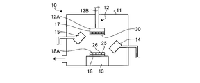
- FIG. 1 is a cross-sectional view schematically showing a configuration of a room temperature bonding apparatus to which the semiconductor device according to the present embodiment is bonded.
- FIG. 2 is a cross-sectional view schematically showing the configuration of the first wafer and the second wafer before bonding.
- FIG. 3 is a cross-sectional view schematically showing a configuration of a semiconductor device formed by bonding a first wafer and a second wafer.
- FIG. 4 is a cross-sectional view schematically showing a state where the first wafer and the second wafer are bonded.
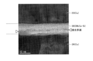
- FIG. 5 is a transmission electron micrograph showing the SiO 2 / SiO 2 bonding interface as the insulating layer.
- FIG. 6 is a transmission electron micrograph showing a Cu / Cu bonding interface as a bonding electrode.
- FIG. 7 is a graph showing the EELS spectrum of the Si-L absorption edge at the measurement point.
- FIG. 8 is a graph showing the EELS spectrum of the OK absorption edge at the measurement point.
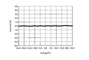
- FIG. 9 is a graph showing the relationship between current and voltage between SiO 2 / SiO 2 .
- FIG. 10 is a graph showing the EELS spectrum of the Si-L absorption edge at the measurement point.
- FIG. 11 is a graph showing the EELS spectrum of the Cu-L absorption edge at the measurement point.
- FIG. 12 is a graph showing the relationship between current and voltage between Cu / Cu.
- FIG. 13A is a process explanatory diagram illustrating a process of bonding the first wafer and the second wafer.
- FIG. 13B is a process explanatory diagram illustrating a process of bonding the first wafer and the second wafer.
- FIG. 13C is a process explanatory diagram illustrating a process of bonding the first wafer and the second wafer.
- FIG. 13-4 is a process explanatory diagram illustrating a process of bonding the first wafer and the second wafer.
- FIG. 13-5 is a process explanatory diagram illustrating a process of bonding the first wafer and the second wafer.
- FIG. 13-6 is a process explanatory diagram illustrating a process of bonding the first wafer and the second wafer.
- FIG. 14A is a process explanatory diagram illustrating another process of bonding the first wafer and the second wafer.
- FIG. 14B is a process explanatory diagram illustrating another process of bonding the first wafer and the second wafer.
- FIG. 14C is a process explanatory diagram illustrating another process of bonding the first wafer and the second wafer.
- FIG. 14-4 is a process explanatory diagram showing another process of bonding the first wafer and the second wafer.
- FIG. 15A is a cross-sectional view schematically showing a configuration before bonding of the first wafer and the second wafer according to another embodiment.
- FIG. 15B is a cross-sectional view schematically showing a configuration in a state where the first wafer and the second wafer according to another embodiment are bonded.
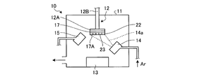
- FIG. 1 is a cross-sectional view schematically showing a configuration of a room temperature bonding apparatus to which a semiconductor device according to this embodiment is bonded.
- the room temperature bonding apparatus 10 includes a vacuum chamber 11, an upper stage 12 and a lower stage 13 installed in the vacuum chamber 11, a fast atom beam source (FAB: Fast) Atom Beam) 14, 15 and a vacuum exhaust device 16.
- FAB Fast atom beam source
- the vacuum chamber 11 is a container that seals the inside from the environment, and the vacuum exhaust device 16 discharges gas from the inside of the vacuum chamber 11. Thereby, the inside of the vacuum chamber 11 becomes a vacuum atmosphere. Furthermore, the vacuum chamber 11 includes a gate (not shown) that allows the internal space of the vacuum chamber 11 to communicate with the outside.
- the upper stage 12 includes an electrostatic chuck 12A formed in a disk shape and a pressure contact mechanism 12B that moves the electrostatic chuck 12A up and down in the vertical direction.
- the electrostatic chuck 12A includes a dielectric layer at the lower end of the disk, applies a voltage to the dielectric layer, and adsorbs and supports the first wafer (substrate) 17 on the dielectric layer by electrostatic force.
- the pressure contact mechanism 12B translates the electrostatic chuck 12A in the vertical direction with respect to the vacuum chamber 11 by a user operation.
- the lower stage 13 is a stage that supports the second wafer (substrate) 18 on its upper surface, and includes a transfer mechanism (not shown).
- the transfer mechanism translates the lower stage 13 in the horizontal direction by the user's operation, and rotates the lower stage 13 around a rotation axis parallel to the vertical direction.
- the lower stage 13 may be provided with a dielectric layer at its upper end, a mechanism for applying a voltage to the dielectric layer, and attracting and supporting the second wafer 18 on the dielectric layer by electrostatic force.
- the fast atom beam sources 14 and 15 emit a neutral atom beam (for example, argon Ar atom) used for activating the wafer surface.
- a neutral atom beam for example, argon Ar atom
- One fast atom beam source 14 is disposed toward the first wafer 17 supported by the upper stage 12, and the other fast atom beam source 15 is directed toward the second wafer 18 supported by the lower stage 13. Be placed. Irradiation with the neutral atom beam activates the surfaces of the first wafer 17 and the second wafer 18.
- other activating means for example, ion gun or plasma may be used for activating each wafer.
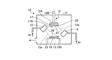
- FIG. 2 is a cross-sectional view schematically showing the configuration of the first wafer and the second wafer before bonding
- FIG. 3 shows the configuration of the semiconductor device formed by bonding the first wafer and the second wafer. It is sectional drawing shown typically.
- the first wafer 17 includes a first insulating layer (insulating material) 22 formed on the first semiconductor substrate 21 and a first insulating layer 22 formed on the first insulating layer 22. And a bonding electrode (conductive material) 23.
- the first insulating layer 22 and the first bonding electrode 23 are formed so as to be exposed on the surface 17A of the first wafer 17, and the surface 17A functions as a bonding surface.
- the second wafer 18 includes a second insulating layer (insulating material) 25 formed on the second semiconductor substrate 24 and a second bonding electrode (conductive material) formed on the second insulating layer 25. 26).
- the second insulating layer 25 and the second bonding electrode 26 are respectively exposed on the surface 18A of the second wafer 18, and the surface 18A functions as a bonding surface.
- These surfaces 17A and 18A are formed as flat surfaces, and the surfaces 17A and 18A are in close contact with each other.
- single crystal silicon Si
- germanium Ga
- gallium arsenide GaAs
- silicon carbide SiC
- Such materials can also be used.
- the first semiconductor substrate 21 and the second semiconductor substrate 24 may use not only the same type of material but also different types of materials.
- the first insulating layer 22 and the second insulating layer 25 are formed of oxide or nitride of a semiconductor substrate on the surface 17A, 18A side.
- a silicon oxide film (SiO 2 ) or a silicon nitride film (Si 3 ) is used as the first insulating layer 22 and the second insulating layer 25.
- N 4 is formed by film formation in an oxidation furnace, a nitriding furnace, a chemical vapor deposition (CVD) apparatus, or the like.
- CVD chemical vapor deposition
- the 1st joining electrode 23 and the 2nd joining electrode 26 are formed with the material excellent in electroconductivity, for example, copper (Cu).
- a wiring material is connected to the first bonding electrode 23 and the second bonding electrode 26 to form an electronic circuit and various elements.
- the surfaces 17 ⁇ / b> A and 18 ⁇ / b> A as bonding surfaces are opposed to each other, and the room temperature bonding apparatus 10 described above is used. Room temperature bonding is performed.
- the first bonding electrode 23 of the first wafer 17 and the second bonding electrode 26 of the second wafer 18 are bonded, and the first insulation layer 22 of the first wafer 17 and the second insulation of the second wafer 18 are combined. Layer 25 is bonded.
- the first insulating layer 22 and the second insulating layer 25 are formed of a silicon oxide film (SiO 2 ) or a silicon nitride film (Si 3). Since they are N 4 ), they cannot be joined directly. For this reason, in this configuration, as shown in FIG. 4, the bonding intermediate layer 30 for bonding the bonding electrode and the insulating layer simultaneously between the surface 17 ⁇ / b> A of the first wafer 17 and the surface 18 ⁇ / b> A of the second wafer 18. Is provided.
- the bonding intermediate layer 30 is a thin film for bonding the surface 17A of the first wafer 17 and the surface 18A of the second wafer 18 and is formed of an amorphous semiconductor material (for example, amorphous silicon).
- an amorphous semiconductor material for example, amorphous silicon
- amorphous silicon exhibits non-conductivity by itself (single substance), but exhibits conductivity by bonding with metals or the like.
- the first insulating layer 22 and the first insulating layer 22 are maintained while maintaining the non-conductivity (insulating property) between the first insulating layer 22 and the second insulating layer 25.
- the second insulating layer 25 can be firmly bonded. Furthermore, the electrical characteristics between the first bonding electrode 23 and the second bonding electrode 26 are not deteriorated, and the conductivity between the first bonding electrode 23 and the second bonding electrode 26 can be ensured.
- the bonding intermediate layer 30 has a region (insulating bonding portion 30a) for bonding the first insulating layer 22 and the second insulating layer 25 while maintaining non-conductivity (insulation), and has conductivity. A region where the first bonding electrode 23 and the second bonding electrode 26 are bonded (conductive bonding portion 30b) is formed.
- FIG. 5 is a transmission electron micrograph showing a SiO 2 / SiO 2 bonding interface as an insulating layer
- FIG. 6 is a transmission electron micrograph showing a Cu / Cu bonding interface as a bonding electrode.
- a transmission electron microscope (TEM) is a type of electron microscope in which an electron beam is applied to an observation target and an interference image created by electrons transmitted through the electron beam is magnified and observed.
- an amorphous silicon (a-Si) layer is formed as a bonding intermediate layer 30 (insulating bonding portion 30a) at the bonding interface of SiO 2 / SiO 2 as the first insulating layer 22 and the second insulating layer 25. Is formed.
- amorphous silicon (a ⁇ Si) layer is formed similarly to the bonding interface of Cu / Cu as the first bonding electrode 23 and the second bonding electrode 26 .
- These bonding intermediate layers 30 are all formed to have a thickness of about 7 to 9 nm, and there is no presence of voids (voids) between the bonding intermediate layer 30 and SiO 2 or Cu. Has been obtained.
- the bonding intermediate layer 30 is formed on the bonding surface of the insulating layer (SiO 2 ) and the bonding electrode (Cu) by sputtering of single crystal silicon, and changes the state from single crystal silicon to amorphous silicon. It is formed by changing.
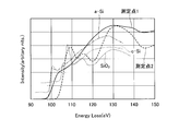
- the inventor is in the state of the vicinity of the interface by electron energy loss spectroscopy (EELS) at two points of measurement point 1 in the bonding intermediate layer 30 and measurement point 2 in the insulating layer (SiO 2 ). Analysis was carried out.
- Electron energy loss spectroscopy is a technique for analyzing constituent elements and electronic structures of substances by measuring the energy lost by the interaction of atoms with electrons when they pass through a thin sample.
- FIG. 7 is a graph showing the EELS spectrum at the Si—L absorption edge at the measurement point
- FIG. 8 is a graph showing the EELS spectrum at the OK absorption edge at the measurement point.
- FIG. 7 shows spectra in the same energy region in single crystal silicon (c-Si), amorphous silicon (a-Si), and silicon oxide film (SiO 2 ).
- the EELS spectrum of the Si-L absorption edge at the measurement point 1 in the junction intermediate layer 30 is close to single crystal silicon or amorphous silicon, and no characteristic peak of SiO 2 was observed.
- the EELS spectrum at the OK absorption edge the presence of oxygen atoms O was hardly confirmed in the junction intermediate layer 30.
- junction intermediate layer 30 does not contain Si oxide, and further, the junction intermediate layer 30 formed between the first insulating layer 22 and the second insulating layer 25 from the high resolution image shown in FIG. (Insulating junction 30a) is considered to be amorphous silicon.
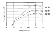
- FIG. 9 is a graph showing the relationship between current and voltage between SiO 2 / SiO 2 .
- non-conductive refers to a state where the resistivity is 10 5 ⁇ ⁇ cm or more.
- the bonding strength of SiO 2 / SiO 2 bonded through the bonding intermediate layer 30 was measured.
- the bonding strength was measured by cutting a bonded SiO 2 / SiO 2 sample into a chip having a size of 12 mm ⁇ 12 mm and performing a tensile test on the chip. In the test, the tip was fixed to a jig, and the load at which the tip broke was measured while changing the tensile load on the jig. In the tensile test, the fracture occurred, but the fracture occurred when the chip and the jig were peeled off at the adhesive interface, and the SiO 2 / SiO 2 bond was maintained. Since the tensile strength at the time of rupture was 25 MPa or more, the strength of the bonding interface by the bonding intermediate layer 30 is considered to be higher than this.
- the bonding intermediate layer 30 As described above, in the configuration in which amorphous silicon (amorphous semiconductor material) is used as the bonding intermediate layer 30, the non-conductivity (insulating property) between the first insulating layer 22 and the second insulating layer 25 is maintained. The result that the 1st insulating layer 22 and the 2nd insulating layer 25 were able to be joined firmly was obtained.
- amorphous silicon amorphous semiconductor material
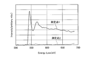
- FIG. 10 is a graph showing the EELS spectrum of the Si—L absorption edge at the measurement point
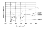
- FIG. 11 is a graph showing the EELS spectrum of the Cu—L absorption edge at the measurement point. In FIG. 11, the spectrum of the same energy region of copper (Cu) is shown for comparison.
- the EELS spectra at the Si-L absorption edges at the measurement points A to C in the junction intermediate layer 30 are all the same shape, indicating that silicon is present alone. Yes. Further, as shown in FIG. 11, in the EELS spectrum at the Cu-L absorption edge, the presence of copper is recognized at any measurement point A to C in the junction intermediate layer 30.
- FIG. 12 is a graph showing the relationship between current and voltage between Cu / Cu. As shown in FIG. 12, a linear relationship is obtained between the voltage and the current even when bonded via the bonding intermediate layer 30, and ohmic (ohmic) is obtained between Cu / Cu. It is thought that a connection (according to the law) has been obtained.
- the resistance value when Cu / Cu was directly joined was 20 (m ⁇ ) or less, whereas in the case of joining via the joining intermediate layer 30, it was 25 (m ⁇ ) or less, and the results were almost the same. there were.
- the conductivity between the first bonding electrode 23 and the second bonding electrode 26 can be secured. Therefore, since the semiconductor device 20 of this embodiment includes the bonding intermediate layer 30 between the surfaces 17A and 18A from which the bonding electrodes 23 and 26 and the insulating layers 22 and 25 are exposed, the bonding electrodes 23 and 26 and the insulating layer 22 are provided. , 25 can be hybridized together. Furthermore, since the bonding intermediate layer 30 exhibits non-conductivity by itself and combines with the bonding electrodes 23 and 26 to exhibit conductivity, the conductivity between the first bonding electrode 23 and the second bonding electrode 26 is ensured.
- amorphous silicon amorphous semiconductor material
- FIGS. 13-1 to 13-6 are process explanatory views showing the process of bonding the first wafer and the second wafer.
- the first wafer 17 and the second wafer 18 are pre-manufactured by another work process in a state where the bonding electrodes 23 and 26 and the insulating layers 22 and 25 are exposed on the surfaces 17A and 18A, respectively.
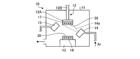
- the first wafer 17 is transferred into the vacuum chamber 11 of the room-temperature bonding apparatus 10, and the first wafer 17 has an electrostatic capacity of the upper stage 12 so that the surface 17A faces vertically downward. Supported by the chuck 12A. The inside of the vacuum chamber 11 is maintained in a vacuum atmosphere. In this state, an argon beam 14a is emitted from the fast atom beam source 14 toward the surface 17A of the first wafer 17. The argon beam 14a is applied to the surface 17A of the first wafer 17, and the surface 17A is activated.
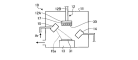
- the bare wafer 31 is transferred into the vacuum chamber 11, and the bare wafer 31 is placed on the upper surface of the lower stage 13.
- the bare wafer 31 is formed of single crystal silicon, and is used as a sputtering source when the bonding intermediate layer 30 is generated.
- an argon beam 15 a is emitted from the fast atom beam source 15 toward the bare wafer 31.
- the bare wafer 31 is sputtered, the silicon atoms ejected from the bare wafer 31 rise, and the bonding intermediate layer 30 is formed on the surface 17 ⁇ / b> A of the first wafer 17.
- the argon beam 15a is irradiated for a predetermined time (for example, 10 minutes), and the bonding intermediate layer 30 having a thickness of about 1 nm to 50 nm is formed on the surface 17A of the first wafer 17.
- the bonding intermediate layer 30 is amorphous (amorphous) silicon.
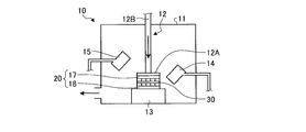
- the bare wafer 31 is unloaded from the vacuum chamber 11, and the second wafer 18 is transferred into the vacuum chamber 11 instead.
- the second wafer 18 is placed on the upper surface of the lower stage 13 so that the surface 18A faces vertically upward.
- an argon beam 15a is emitted from the fast atom beam source 15 toward the surface 18A of the second wafer 18.
- the argon beam 15a is applied to the surface 18A of the second wafer 18, and the surface 18A is activated.
- an argon beam 14 a is emitted from the fast atom beam source 14 toward the bonding intermediate layer 30 formed on the surface of the first wafer 17.
- part of the amorphous silicon forming the bonding intermediate layer 30 functions as a sputtering source.
- the bonding intermediate layer 30 is sputtered, the silicon atoms ejected from the bonding intermediate layer 30 rise, and the bonding intermediate layer 30 is also formed on the surface 18 ⁇ / b> A of the second wafer 18.
- the argon beam 14a is irradiated for a predetermined time (for example, 10 minutes), and the bonding intermediate layer 30 having a thickness of about 1 nm to 50 nm is formed on the surface 18A of the second wafer 18.
- the bonding intermediate layer 30 is also amorphous (amorphous) silicon.
- the bonding intermediate layer 30 formed on the surface of the first wafer 17 is used as a sputtering source, it is not necessary to prepare a separate sputtering source for the surface 18A of the second wafer 18, and the vacuum chamber 11 Since the sputter source is reduced in and out, the work procedure is simplified, and the bonding intermediate layer 30 can be easily formed on the surfaces 17A and 18A of the first wafer 17 and the second wafer 18, respectively.
- the pressure contact mechanism 12B of the upper stage 12 is operated, so that the static wafer supporting the first wafer 17 is operated.
- the electric chuck 12 ⁇ / b> A is lowered vertically and the first wafer 17 and the second wafer 18 are pressed against each other. Thereby, the surface 17A of the first wafer 17 and the surface 18A of the second wafer 18 are bonded via the bonding intermediate layer 30, and the semiconductor device 20 is formed.
- the semiconductor device 20 (the first wafer 17 and the second wafer 18) is heated in the vacuum chamber 11 at a predetermined temperature (for example, about 50 ° C. to 400 ° C.).
- the surface 17A of the first wafer 17 and the surface 18A of the second wafer 18 are activated, and the activated surfaces 17A and 18A are activated. Since the bonding intermediate layer 30 and the step of pressing the first wafer 17 and the second wafer 18 through the bonding intermediate layer 30 are provided, the bonding electrodes 23 and 26 and the insulating layers 22 and 25 are respectively formed. Hybrid joining that joins at the same time can be easily realized.
- the bare wafer 31 is irradiated with the argon beam 15a and the bare wafer 31 is sputtered to form the bonding intermediate layer 30 on the surface 17A of the first wafer 17, and then formed on the surface 17A.
- Operation procedure for forming the bonding intermediate layer 30 on the surface 18A of the second wafer 18 by irradiating the bonding intermediate layer 30 with the argon beam 14a and sputtering a part of the amorphous silicon forming the bonding intermediate layer 30.
- the bonding intermediate layer 30 can be easily formed on the respective surfaces 17A and 18A of the first wafer 17 and the second wafer 18.
- FIGS. 14-1 to 14-4 are process explanatory views showing another process of bonding the first wafer and the second wafer.
- the first wafer 17 and the second wafer 18 are preliminarily formed in a state where the bonding electrodes 23 and 26 and the insulating layers 22 and 25 are exposed on the surfaces 17A and 18A, respectively, by another work process. It is manufactured.
- the first wafer 17 is transferred into the vacuum chamber 11 of the room temperature bonding apparatus 10, and the first wafer 17 is electrostatically charged to the upper stage 12 so that the surface 17A faces vertically downward. Supported by the chuck 12A.
- the second wafer 18 is transferred into the vacuum chamber 11, and this second wafer 18 is placed on the upper surface of the lower stage 13 so that the surface 18A faces vertically upward.
- the inside of the vacuum chamber 11 is maintained in a vacuum atmosphere.
- argon beams 14a and 15a are emitted from the fast atom beam sources 14 and 15 toward the surface 17A of the first wafer 17 and the surface 18A of the second wafer 18, respectively.
- the argon beams 14a and 15a are applied to the surface 17A of the first wafer 17 and the surface 18A of the second wafer 18, respectively, and the surfaces 17A and 18A are activated.
- the first wafer 17 and the second wafer 18 whose surfaces 17A and 18A are activated are transferred from the vacuum chamber 11 to the film forming chamber 40.
- the 1st wafer 17 and the 2nd wafer 18 are conveyed by the vacuum conveyance path so that external air (oxygen) may not be touched.
- the film forming chamber 40 is a chamber for forming the bonding intermediate layer 30 on the surface 17A of the first wafer 17 and the surface 18A of the second wafer 18, and chemical vapor deposition is performed in the film forming chamber 40.
- a device (not shown) is arranged.
- a source gas containing silicon is supplied to the surface 17A of the first wafer 17 and the surface 18A of the second wafer 18 with the first wafer 17 and the second wafer 18 heated under predetermined conditions.
- the bonding intermediate layer 30 is formed by a chemical reaction on the surfaces 17A and 18A. Also in this chemical vapor deposition method, the bonding intermediate layer 30 is formed of amorphous (amorphous) silicon. In this configuration, since the bonding intermediate layer 30 can be formed separately, the processing time of the bonding process can be shortened.
- the first wafer 17 and the second wafer 18 on which the bonding intermediate layer 30 is formed are transferred into the vacuum chamber 11.
- the first wafer 17 is supported by the electrostatic chuck 12A of the upper stage 12 so that the bonding intermediate layer 30 faces vertically downward, and the second wafer 18 has a bonding intermediate layer 30 facing vertically upward. It is placed on the upper surface of the lower stage 13.
- the inside of the vacuum chamber 11 is maintained in a vacuum atmosphere.
- argon beams 14a and 15a are emitted from the fast atom beam sources 14 and 15 toward the bonding intermediate layers 30 and 30 formed on the first wafer 17 and the second wafer 18, respectively.
- the argon beams 14a and 15a are applied to the surfaces of the bonding intermediate layers 30 and 30 of the first wafer 17 and the second wafer 18, respectively, and the surfaces of the bonding intermediate layers 30 and 30 are activated.
- the pressure contact mechanism 12B of the upper stage 12 is operated so that the static wafer supporting the first wafer 17 is supported.
- the electric chuck 12 ⁇ / b> A is lowered vertically and the first wafer 17 and the second wafer 18 are pressed against each other.
- the surface 17A of the first wafer 17 and the surface 18A of the second wafer 18 are bonded via the bonding intermediate layer 30, and the semiconductor device 20 is formed.
- the semiconductor device 20 (the first wafer 17 and the second wafer 18) is heated in the vacuum chamber 11 at a predetermined temperature (for example, 50 ° C. to 400 ° C.).
- the alloying of the copper Cu of the first bonding electrode 23 and the second bonding electrode 26 and the amorphous silicon of the bonding intermediate layer 30 is promoted, and the bonding of the first bonding electrode 23 and the second bonding electrode 26 is further enhanced. Strengthens and improves electrical properties.
- FIG. 15-1 is a cross-sectional view schematically showing a configuration before bonding of the first wafer and the second wafer according to another embodiment
- FIG. 15-2 shows the first wafer according to another embodiment. It is sectional drawing which shows typically the structure of the state which joined the 2nd wafer.
- the surface 17A of the first wafer 17 and the surface 18A of the second wafer 18 are each formed as a flat surface, and the surfaces 17A and 18A are formed in close contact with each other.
- the first insulating layer 122 and the first bonding electrode 123 laminated on the first semiconductor substrate 121 are exposed on the surface 17A.
- the height position of the surface 122A of the first insulating layer 122 is formed lower than the height position of the surface 123A of the first bonding electrode 123.
- the height position difference t is set to about 1 nm to 100 nm, which is about the same as that of the bonding intermediate layer 30.
- the second insulating layer 125 and the second bonding electrode 126 stacked on the second semiconductor substrate 124 are exposed on the surface 18A, and the height position of the surface 125A of the second insulating layer 125 is the height position. It is formed lower than the height position of the surface 126A of the second bonding electrode 126.
- the height position difference t is set to about 1 nm to 100 nm, which is about the same as that of the bonding intermediate layer 30. Since other configurations are the same as the configurations of the above-described embodiment, description thereof will be omitted.
- the pressure contact load is applied to the first bonding electrode 123 and the second bonding electrode 126. Therefore, as shown in FIG.
- the bonding intermediate layer 30 is broken by the first bonding electrode 123 and the second bonding electrode 126, and the first bonding electrode 123 and the second bonding electrode 126 are directly bonded to each other. Thereby, it is possible to obtain good electrical characteristics and bonding strength in the bonding between the first bonding electrode 123 and the second bonding electrode 126.
- the bonding intermediate layer 30 is formed on both the surfaces 17A and 18A of the first wafer 17 and the second wafer 18, but may be formed on one.
- the 1st joining electrode 123 and the 2nd joining electrode 126 were made into the shape which protrudes rather than the 1st insulating layer 122 and the 2nd insulating layer 125, respectively, the 1st joining electrode 123 or the 2nd joining electrode is used. One of the electrodes 126 may be used.
- middle layer 30 by sputtering or a chemical vapor deposition method
- a vapor deposition material for example, silicon
- the bonding intermediate layer 30 is formed of amorphous (amorphous) silicon.
- the bonding intermediate layer 30 can be formed separately, the processing time of the bonding process can be shortened.
Landscapes
- Engineering & Computer Science (AREA)
- Microelectronics & Electronic Packaging (AREA)
- Computer Hardware Design (AREA)
- Power Engineering (AREA)
- Physics & Mathematics (AREA)
- Condensed Matter Physics & Semiconductors (AREA)
- General Physics & Mathematics (AREA)
- Manufacturing & Machinery (AREA)
- Mechanical Engineering (AREA)
- Pressure Welding/Diffusion-Bonding (AREA)
Priority Applications (4)
| Application Number | Priority Date | Filing Date | Title |
|---|---|---|---|
| CN201580069954.0A CN107112199B (zh) | 2014-12-22 | 2015-10-07 | 半导体装置及半导体装置的制造方法 |
| KR1020177017033A KR101994011B1 (ko) | 2014-12-22 | 2015-10-07 | 반도체 장치 및 반도체 장치의 제조 방법 |
| US15/537,646 US10486263B2 (en) | 2014-12-22 | 2015-10-07 | Room-temperature-bonded semiconductor device and manufacturing method of room-temperature-bonded semiconductor device |
| EP15872415.3A EP3240015B1 (en) | 2014-12-22 | 2015-10-07 | Semiconductor device and semiconductor device manufacturing method |
Applications Claiming Priority (2)
| Application Number | Priority Date | Filing Date | Title |
|---|---|---|---|
| JP2014-259115 | 2014-12-22 | ||
| JP2014259115A JP6165127B2 (ja) | 2014-12-22 | 2014-12-22 | 半導体装置及び半導体装置の製造方法 |
Publications (1)
| Publication Number | Publication Date |
|---|---|
| WO2016103846A1 true WO2016103846A1 (ja) | 2016-06-30 |
Family
ID=56149883
Family Applications (1)
| Application Number | Title | Priority Date | Filing Date |
|---|---|---|---|
| PCT/JP2015/078518 WO2016103846A1 (ja) | 2014-12-22 | 2015-10-07 | 半導体装置及び半導体装置の製造方法 |
Country Status (7)
Families Citing this family (17)
| Publication number | Priority date | Publication date | Assignee | Title |
|---|---|---|---|---|
| US10886250B2 (en) | 2015-07-10 | 2021-01-05 | Invensas Corporation | Structures and methods for low temperature bonding using nanoparticles |
| TWI822659B (zh) | 2016-10-27 | 2023-11-21 | 美商艾德亞半導體科技有限責任公司 | 用於低溫接合的結構和方法 |
| US10515913B2 (en) | 2017-03-17 | 2019-12-24 | Invensas Bonding Technologies, Inc. | Multi-metal contact structure |
| US10446441B2 (en) | 2017-06-05 | 2019-10-15 | Invensas Corporation | Flat metal features for microelectronics applications |
| US10790262B2 (en) | 2018-04-11 | 2020-09-29 | Invensas Bonding Technologies, Inc. | Low temperature bonded structures |
| US11244916B2 (en) | 2018-04-11 | 2022-02-08 | Invensas Bonding Technologies, Inc. | Low temperature bonded structures |
| US11244920B2 (en) | 2018-12-18 | 2022-02-08 | Invensas Bonding Technologies, Inc. | Method and structures for low temperature device bonding |
| CN111370339B (zh) * | 2020-03-20 | 2022-02-22 | 中国科学院半导体研究所 | 晶圆的室温等静压金属键合方法 |
| US11735523B2 (en) | 2020-05-19 | 2023-08-22 | Adeia Semiconductor Bonding Technologies Inc. | Laterally unconfined structure |
| US12211809B2 (en) | 2020-12-30 | 2025-01-28 | Adeia Semiconductor Bonding Technologies Inc. | Structure with conductive feature and method of forming same |
| WO2022187402A1 (en) * | 2021-03-03 | 2022-09-09 | Invensas Bonding Technologies, Inc. | Contact structures for direct bonding |
| JP7222493B2 (ja) | 2021-04-28 | 2023-02-15 | 日本電産マシンツール株式会社 | 半導体装置の製造方法、及び常温接合装置 |
| JP2023137581A (ja) * | 2022-03-18 | 2023-09-29 | キオクシア株式会社 | 半導体装置、半導体装置の製造方法 |
| FR3134227A1 (fr) * | 2022-04-04 | 2023-10-06 | Commissariat A L'energie Atomique Et Aux Energies Alternatives | Procédé de collage d’un premier substrat au niveau d’une surface présentant une nanotopologie élastique |
| CN114999948A (zh) * | 2022-06-06 | 2022-09-02 | 闽南师范大学 | 一种高真空磁控溅射热压键合一体机以及键合方法 |
| CN116092953B (zh) * | 2023-03-07 | 2023-07-18 | 天津中科晶禾电子科技有限责任公司 | 一种晶圆键合装置、方法及复合衬底组件 |
| JP7526450B1 (ja) * | 2024-03-22 | 2024-08-01 | エスエイチダブリュウテクノロジーズ(シャンハイ)ユウゲンコウシ | 半導体ウエーハの接合装置及び接合方法 |
Citations (5)
| Publication number | Priority date | Publication date | Assignee | Title |
|---|---|---|---|---|
| JPH01133341A (ja) * | 1987-11-19 | 1989-05-25 | Hitachi Ltd | 半導体基板の製造方法及び半導体装置の製造方法 |
| JPH0684733A (ja) * | 1992-09-03 | 1994-03-25 | Hitachi Ltd | 半導体集積回路装置とその製造方法及び半導体集積回路製造装置 |
| JPH1092702A (ja) * | 1996-09-18 | 1998-04-10 | Agency Of Ind Science & Technol | シリコンウェハーの常温接合法 |
| JPH10256263A (ja) * | 1997-03-11 | 1998-09-25 | Nec Corp | Soi基板およびその製造方法 |
| JP2012238729A (ja) * | 2011-05-12 | 2012-12-06 | Nippon Telegr & Teleph Corp <Ntt> | 半導体装置およびその製造方法 |
Family Cites Families (59)
| Publication number | Priority date | Publication date | Assignee | Title |
|---|---|---|---|---|
| DE19648759A1 (de) * | 1996-11-25 | 1998-05-28 | Max Planck Gesellschaft | Verfahren zur Herstellung von Mikrostrukturen sowie Mikrostruktur |
| FR2783969B1 (fr) * | 1998-09-28 | 2002-01-18 | Commissariat Energie Atomique | Dispositif hybride et procede de realisation de composants electriquement actifs par assemblage |
| US6387736B1 (en) * | 1999-04-26 | 2002-05-14 | Agilent Technologies, Inc. | Method and structure for bonding layers in a semiconductor device |
| JP4275806B2 (ja) * | 1999-06-01 | 2009-06-10 | 株式会社ルネサステクノロジ | 半導体素子の実装方法 |
| FR2798224B1 (fr) * | 1999-09-08 | 2003-08-29 | Commissariat Energie Atomique | Realisation d'un collage electriquement conducteur entre deux elements semi-conducteurs. |
| JP3440057B2 (ja) | 2000-07-05 | 2003-08-25 | 唯知 須賀 | 半導体装置およびその製造方法 |
| WO2003100486A1 (en) * | 2002-05-28 | 2003-12-04 | Matsushita Electric Works, Ltd. | Material for substrate mounting optical circuit-electric circuit mixedly and substrate mounting optical circuit-electric circuit mixedly |
| US7114361B2 (en) * | 2003-09-12 | 2006-10-03 | Board Of Supervisors Of Louisiana State University And Agricultural And Mechanical College | Microscale compression molding of metals with surface engineered LIGA inserts |
| FR2864336B1 (fr) * | 2003-12-23 | 2006-04-28 | Commissariat Energie Atomique | Procede de scellement de deux plaques avec formation d'un contact ohmique entre celles-ci |
| EP1557449A1 (en) * | 2004-01-22 | 2005-07-27 | 3M Innovative Properties Company | Adhesive tape for structural bonding |
| JP3790995B2 (ja) * | 2004-01-22 | 2006-06-28 | 有限会社ボンドテック | 接合方法及びこの方法により作成されるデバイス並びに接合装置 |
| FR2872625B1 (fr) * | 2004-06-30 | 2006-09-22 | Commissariat Energie Atomique | Assemblage par adhesion moleculaire de deux substrats, l'un au moins supportant un film conducteur electrique |
| US7550366B2 (en) * | 2005-12-02 | 2009-06-23 | Ayumi Industry | Method for bonding substrates and device for bonding substrates |
| US7345344B2 (en) * | 2006-02-16 | 2008-03-18 | Freescale Semiconductor, Inc. | Embedded substrate interconnect for underside contact to source and drain regions |
| JP4162094B2 (ja) | 2006-05-30 | 2008-10-08 | 三菱重工業株式会社 | 常温接合によるデバイス、デバイス製造方法ならびに常温接合装置 |
| JP4172806B2 (ja) * | 2006-09-06 | 2008-10-29 | 三菱重工業株式会社 | 常温接合方法及び常温接合装置 |
| EP1993127B1 (en) * | 2007-05-18 | 2013-04-24 | Semiconductor Energy Laboratory Co., Ltd. | Manufacturing method of SOI substrate |
| JP4967842B2 (ja) * | 2007-06-18 | 2012-07-04 | セイコーエプソン株式会社 | シリコン基材の接合方法、液滴吐出ヘッド、液滴吐出装置および電子デバイス |
| RU2010114227A (ru) * | 2007-09-12 | 2011-10-20 | Смольтек Аб (Se) | Соединение и связывание соседних слоев наноструктурами |
| JP4786693B2 (ja) * | 2008-09-30 | 2011-10-05 | 三菱重工業株式会社 | ウェハ接合装置およびウェハ接合方法 |
| JP5342210B2 (ja) * | 2008-10-30 | 2013-11-13 | 三菱重工業株式会社 | アライメント装置制御装置およびアライメント方法 |
| JP5389627B2 (ja) * | 2008-12-11 | 2014-01-15 | 信越化学工業株式会社 | ワイドバンドギャップ半導体を積層した複合基板の製造方法 |
| JP4796120B2 (ja) * | 2008-12-11 | 2011-10-19 | 三菱重工業株式会社 | 常温接合装置 |
| JP2010278337A (ja) * | 2009-05-29 | 2010-12-09 | Shin-Etsu Chemical Co Ltd | 表面欠陥密度が少ないsos基板 |
| US9608119B2 (en) * | 2010-03-02 | 2017-03-28 | Micron Technology, Inc. | Semiconductor-metal-on-insulator structures, methods of forming such structures, and semiconductor devices including such structures |
| US8507966B2 (en) * | 2010-03-02 | 2013-08-13 | Micron Technology, Inc. | Semiconductor cells, arrays, devices and systems having a buried conductive line and methods for forming the same |
| US8647962B2 (en) * | 2010-03-23 | 2014-02-11 | Taiwan Semiconductor Manufacturing Company, Ltd. | Wafer level packaging bond |
| JP4831844B1 (ja) * | 2010-09-28 | 2011-12-07 | 三菱重工業株式会社 | 常温接合装置および常温接合方法 |
| US8563396B2 (en) * | 2011-01-29 | 2013-10-22 | International Business Machines Corporation | 3D integration method using SOI substrates and structures produced thereby |
| WO2012105473A1 (ja) * | 2011-01-31 | 2012-08-09 | ボンドテック株式会社 | 接合基板作製方法、接合基板、基板接合方法、接合基板作製装置、及び基板接合体 |
| JP6122297B2 (ja) * | 2011-01-31 | 2017-04-26 | 唯知 須賀 | 接合基板作成方法、基板接合方法、及び接合基板作成装置 |
| KR20130016682A (ko) * | 2011-08-08 | 2013-02-18 | 에스케이하이닉스 주식회사 | 듀얼 레이어 구조의 반도체칩과 듀얼 레이어 구조의 반도체칩을 갖는 패키지들 및 그 제조방법 |
| JP2013098186A (ja) * | 2011-10-27 | 2013-05-20 | Mitsubishi Heavy Ind Ltd | 常温接合装置 |
| WO2013187079A1 (ja) * | 2012-06-15 | 2013-12-19 | 住友化学株式会社 | 複合基板の製造方法および複合基板 |
| KR101755955B1 (ko) * | 2012-06-15 | 2017-07-07 | 미쯔비시 케미컬 주식회사 | 적층체 |
| KR102104147B1 (ko) * | 2012-07-25 | 2020-04-23 | 신에쓰 가가꾸 고교 가부시끼가이샤 | 하이브리드 기판의 제조 방법 및 하이브리드 기판 |
| US8724060B2 (en) * | 2012-08-02 | 2014-05-13 | Shenzhen China Star Optoelectronics Technology Co., Ltd. | Method for manufacturing liquid crystal display module with photovoltaic cell and liquid crystal display module manufactured with same |
| JP6037734B2 (ja) * | 2012-09-07 | 2016-12-07 | 三菱重工工作機械株式会社 | 常温接合装置および常温接合方法 |
| JP6065176B2 (ja) * | 2012-09-27 | 2017-01-25 | 三菱重工工作機械株式会社 | 常温接合装置および常温接合方法 |
| WO2014061337A1 (ja) * | 2012-10-15 | 2014-04-24 | 信越化学工業株式会社 | ナノカーボン膜の作製方法及びナノカーボン膜 |
| JP2014107393A (ja) * | 2012-11-27 | 2014-06-09 | Mitsubishi Heavy Ind Ltd | 常温接合デバイス、常温接合デバイスを有するウェハおよび常温接合方法 |
| US9446467B2 (en) * | 2013-03-14 | 2016-09-20 | Taiwan Semiconductor Manufacturing Company, Ltd. | Integrate rinse module in hybrid bonding platform |
| US20150048509A1 (en) * | 2013-08-16 | 2015-02-19 | Globalfoundries Singapore Pte. Ltd. | Cmos compatible wafer bonding layer and process |
| US9293303B2 (en) * | 2013-08-30 | 2016-03-22 | Taiwan Semiconductor Manufacturing Company, Ltd. | Low contamination chamber for surface activation |
| WO2015040784A1 (ja) * | 2013-09-17 | 2015-03-26 | パナソニックIpマネジメント株式会社 | 半導体装置及びその製造方法 |
| WO2015040798A1 (ja) * | 2013-09-20 | 2015-03-26 | パナソニックIpマネジメント株式会社 | 半導体装置及びその製造方法 |
| WO2015046091A1 (ja) * | 2013-09-27 | 2015-04-02 | 独立行政法人産業技術総合研究所 | ステンレス鋼部材の接合方法およびステンレス鋼 |
| JP2015115446A (ja) * | 2013-12-11 | 2015-06-22 | 株式会社東芝 | 半導体装置の製造方法 |
| US9437572B2 (en) * | 2013-12-18 | 2016-09-06 | Taiwan Semiconductor Manufacturing Company, Ltd. | Conductive pad structure for hybrid bonding and methods of forming same |
| JP6125443B2 (ja) * | 2014-01-17 | 2017-05-10 | 三菱重工工作機械株式会社 | 常温接合装置 |
| US9478471B2 (en) * | 2014-02-19 | 2016-10-25 | Taiwan Semiconductor Manufacturing Company, Ltd. | Apparatus and method for verification of bonding alignment |
| US9190345B1 (en) * | 2014-03-28 | 2015-11-17 | Taiwan Semiconductor Manufacturing Company, Ltd. | Semiconductor devices and methods of manufacture thereof |
| US9257414B2 (en) * | 2014-04-10 | 2016-02-09 | Taiwan Semiconductor Manufacturing Company, Ltd. | Stacked semiconductor structure and method |
| US9455158B2 (en) * | 2014-05-30 | 2016-09-27 | Taiwan Semiconductor Manufacturing Company, Ltd. | 3DIC interconnect devices and methods of forming same |
| US9508685B2 (en) * | 2014-07-29 | 2016-11-29 | Empire Technology Development Llc | Vertically integrated wafers with thermal dissipation |
| US9853133B2 (en) * | 2014-09-04 | 2017-12-26 | Sunedison Semiconductor Limited (Uen201334164H) | Method of manufacturing high resistivity silicon-on-insulator substrate |
| US9852988B2 (en) * | 2015-12-18 | 2017-12-26 | Invensas Bonding Technologies, Inc. | Increased contact alignment tolerance for direct bonding |
| US10020336B2 (en) * | 2015-12-28 | 2018-07-10 | Semiconductor Energy Laboratory Co., Ltd. | Imaging device and electronic device using three dimentional (3D) integration |
| JP2017139266A (ja) * | 2016-02-01 | 2017-08-10 | 株式会社東芝 | 複合基板、半導体装置、およびこれらの製造方法 |
-
2014
- 2014-12-22 JP JP2014259115A patent/JP6165127B2/ja active Active
-
2015
- 2015-10-07 US US15/537,646 patent/US10486263B2/en active Active
- 2015-10-07 KR KR1020177017033A patent/KR101994011B1/ko active Active
- 2015-10-07 CN CN201580069954.0A patent/CN107112199B/zh active Active
- 2015-10-07 EP EP15872415.3A patent/EP3240015B1/en active Active
- 2015-10-07 WO PCT/JP2015/078518 patent/WO2016103846A1/ja active Application Filing
- 2015-12-22 TW TW104143236A patent/TWI596651B/zh active
Patent Citations (5)
| Publication number | Priority date | Publication date | Assignee | Title |
|---|---|---|---|---|
| JPH01133341A (ja) * | 1987-11-19 | 1989-05-25 | Hitachi Ltd | 半導体基板の製造方法及び半導体装置の製造方法 |
| JPH0684733A (ja) * | 1992-09-03 | 1994-03-25 | Hitachi Ltd | 半導体集積回路装置とその製造方法及び半導体集積回路製造装置 |
| JPH1092702A (ja) * | 1996-09-18 | 1998-04-10 | Agency Of Ind Science & Technol | シリコンウェハーの常温接合法 |
| JPH10256263A (ja) * | 1997-03-11 | 1998-09-25 | Nec Corp | Soi基板およびその製造方法 |
| JP2012238729A (ja) * | 2011-05-12 | 2012-12-06 | Nippon Telegr & Teleph Corp <Ntt> | 半導体装置およびその製造方法 |
Non-Patent Citations (1)
| Title |
|---|
| See also references of EP3240015A4 * |
Also Published As
| Publication number | Publication date |
|---|---|
| JP2016119415A (ja) | 2016-06-30 |
| EP3240015A1 (en) | 2017-11-01 |
| KR20170086619A (ko) | 2017-07-26 |
| US20170355040A1 (en) | 2017-12-14 |
| CN107112199B (zh) | 2021-08-17 |
| JP6165127B2 (ja) | 2017-07-19 |
| US10486263B2 (en) | 2019-11-26 |
| CN107112199A (zh) | 2017-08-29 |
| TWI596651B (zh) | 2017-08-21 |
| KR101994011B1 (ko) | 2019-06-27 |
| EP3240015A4 (en) | 2018-08-01 |
| TW201635338A (zh) | 2016-10-01 |
| EP3240015B1 (en) | 2022-11-23 |
Similar Documents
| Publication | Publication Date | Title |
|---|---|---|
| JP6165127B2 (ja) | 半導体装置及び半導体装置の製造方法 | |
| JP6395333B2 (ja) | 基板接合装置および基板接合方法 | |
| Kondou et al. | Si nanoadhesion layer for enhanced SiO2–SiN wafer bonding | |
| US11145531B2 (en) | Substrate fixing device | |
| JP5560595B2 (ja) | 半導体装置の製造方法 | |
| JP5508607B2 (ja) | 高分子フィルムと高分子フィルムとを接合する方法、高分子フィルムと無機材料基板とを接合する方法、高分子フィルム積層体及び高分子フィルムと無機材料基板との積層体 | |
| CN102282645A (zh) | 导电密封环静电吸盘 | |
| KR20140145588A (ko) | 반도체 디바이스의 제조 방법 | |
| JP6521401B1 (ja) | 熱電素子、発電装置、及び熱電素子の製造方法 | |
| TWI695531B (zh) | 薄形基板及其製造方法、以及基板之搬送方法 | |
| JP7173335B2 (ja) | 銅/セラミックス接合体、絶縁回路基板、銅/セラミックス接合体の製造方法、及び、絶縁回路基板の製造方法 | |
| KR20210135624A (ko) | 기판 본딩 장치 및 방법 | |
| US10710192B2 (en) | Method for adhering a first structure and a second structure | |
| JP2009111251A (ja) | 半導体装置およびその製造方法 | |
| JP2024543105A (ja) | 取り外し可能なシャフトを備えた静電チャック | |
| TWI882197B (zh) | 靜電夾盤及基板固定裝置 | |
| CN119501217A (zh) | 陶瓷基座及陶瓷基座的基体制造方法 | |
| KR101397133B1 (ko) | 정전척의 제조방법 | |
| US20150243399A1 (en) | Conductive film, method for producing the same and array substrate comprising the same | |
| CN102760722A (zh) | 包含铜-铝电路连线的集成电路结构及其制备方法 | |
| JP2008205415A (ja) | 静電チャック | |
| CN113169055B (zh) | 半导体装置及半导体装置的制造方法 | |
| JP2009246325A (ja) | 静電チャック | |
| US20150187725A1 (en) | Method of joining silver paste | |
| KR20240004346A (ko) | 반도체 장치의 제조 방법 및 상온 접합 장치 |
Legal Events
| Date | Code | Title | Description |
|---|---|---|---|
| 121 | Ep: the epo has been informed by wipo that ep was designated in this application |
Ref document number: 15872415 Country of ref document: EP Kind code of ref document: A1 |
|
| REEP | Request for entry into the european phase |
Ref document number: 2015872415 Country of ref document: EP |
|
| WWE | Wipo information: entry into national phase |
Ref document number: 15537646 Country of ref document: US |
|
| ENP | Entry into the national phase |
Ref document number: 20177017033 Country of ref document: KR Kind code of ref document: A |
|
| NENP | Non-entry into the national phase |
Ref country code: DE |