WO2016103843A1 - Ébauche de masque, masque à déphasage, procédé de fabrication d'un masque à déphasage et procédé de fabrication d'un dispositif à semi-conducteur - Google Patents
Ébauche de masque, masque à déphasage, procédé de fabrication d'un masque à déphasage et procédé de fabrication d'un dispositif à semi-conducteur Download PDFInfo
- Publication number
- WO2016103843A1 WO2016103843A1 PCT/JP2015/078471 JP2015078471W WO2016103843A1 WO 2016103843 A1 WO2016103843 A1 WO 2016103843A1 JP 2015078471 W JP2015078471 W JP 2015078471W WO 2016103843 A1 WO2016103843 A1 WO 2016103843A1
- Authority
- WO
- WIPO (PCT)
- Prior art keywords
- phase shift
- film
- mask
- lower layer
- pattern
- Prior art date
Links
- 230000010363 phase shift Effects 0.000 title claims abstract description 318
- 238000000034 method Methods 0.000 title claims description 41
- 238000004519 manufacturing process Methods 0.000 title claims description 38
- 239000004065 semiconductor Substances 0.000 title claims description 32
- 239000000463 material Substances 0.000 claims abstract description 95
- 229910052751 metal Inorganic materials 0.000 claims abstract description 89
- 239000002184 metal Substances 0.000 claims abstract description 82
- 239000000758 substrate Substances 0.000 claims abstract description 78
- XUIMIQQOPSSXEZ-UHFFFAOYSA-N Silicon Chemical compound [Si] XUIMIQQOPSSXEZ-UHFFFAOYSA-N 0.000 claims abstract description 60
- 229910052710 silicon Inorganic materials 0.000 claims abstract description 60
- 239000010703 silicon Substances 0.000 claims abstract description 60
- QVGXLLKOCUKJST-UHFFFAOYSA-N atomic oxygen Chemical compound [O] QVGXLLKOCUKJST-UHFFFAOYSA-N 0.000 claims abstract description 55
- 229910052760 oxygen Inorganic materials 0.000 claims abstract description 55
- 239000001301 oxygen Substances 0.000 claims abstract description 55
- 238000002834 transmittance Methods 0.000 claims abstract description 43
- 239000010410 layer Substances 0.000 claims description 266
- IJGRMHOSHXDMSA-UHFFFAOYSA-N Atomic nitrogen Chemical compound N#N IJGRMHOSHXDMSA-UHFFFAOYSA-N 0.000 claims description 70
- 238000012546 transfer Methods 0.000 claims description 49
- 229910052757 nitrogen Inorganic materials 0.000 claims description 30
- 238000001312 dry etching Methods 0.000 claims description 24
- 239000002344 surface layer Substances 0.000 claims description 10
- 230000007547 defect Effects 0.000 abstract description 71
- 238000005530 etching Methods 0.000 abstract description 53
- 238000012937 correction Methods 0.000 abstract description 32
- 150000004767 nitrides Chemical class 0.000 abstract 1
- 239000010408 film Substances 0.000 description 347
- 239000007789 gas Substances 0.000 description 52
- 238000004544 sputter deposition Methods 0.000 description 32
- ZOKXTWBITQBERF-UHFFFAOYSA-N Molybdenum Chemical compound [Mo] ZOKXTWBITQBERF-UHFFFAOYSA-N 0.000 description 26
- 229910052750 molybdenum Inorganic materials 0.000 description 26
- 239000011733 molybdenum Substances 0.000 description 26
- 239000011651 chromium Substances 0.000 description 23
- XKRFYHLGVUSROY-UHFFFAOYSA-N Argon Chemical compound [Ar] XKRFYHLGVUSROY-UHFFFAOYSA-N 0.000 description 22
- VYZAMTAEIAYCRO-UHFFFAOYSA-N Chromium Chemical compound [Cr] VYZAMTAEIAYCRO-UHFFFAOYSA-N 0.000 description 20
- 230000008033 biological extinction Effects 0.000 description 20
- 229910052804 chromium Inorganic materials 0.000 description 18
- 229910021332 silicide Inorganic materials 0.000 description 17
- 230000003287 optical effect Effects 0.000 description 15
- FVBUAEGBCNSCDD-UHFFFAOYSA-N silicide(4-) Chemical compound [Si-4] FVBUAEGBCNSCDD-UHFFFAOYSA-N 0.000 description 15
- 238000010438 heat treatment Methods 0.000 description 14
- 238000004140 cleaning Methods 0.000 description 13
- 238000005546 reactive sputtering Methods 0.000 description 13
- 239000000460 chlorine Substances 0.000 description 12
- 229910052786 argon Inorganic materials 0.000 description 11
- 239000002356 single layer Substances 0.000 description 11
- 238000001514 detection method Methods 0.000 description 10
- 238000010894 electron beam technology Methods 0.000 description 10
- 239000001307 helium Substances 0.000 description 10
- 229910052734 helium Inorganic materials 0.000 description 10
- SWQJXJOGLNCZEY-UHFFFAOYSA-N helium atom Chemical compound [He] SWQJXJOGLNCZEY-UHFFFAOYSA-N 0.000 description 10
- 230000003647 oxidation Effects 0.000 description 10
- 238000007254 oxidation reaction Methods 0.000 description 10
- 230000000052 comparative effect Effects 0.000 description 9
- 229910021344 molybdenum silicide Inorganic materials 0.000 description 9
- 229910052723 transition metal Inorganic materials 0.000 description 9
- YXTPWUNVHCYOSP-UHFFFAOYSA-N bis($l^{2}-silanylidene)molybdenum Chemical compound [Si]=[Mo]=[Si] YXTPWUNVHCYOSP-UHFFFAOYSA-N 0.000 description 8
- 239000000203 mixture Substances 0.000 description 8
- 238000011282 treatment Methods 0.000 description 8
- ZAMOUSCENKQFHK-UHFFFAOYSA-N Chlorine atom Chemical compound [Cl] ZAMOUSCENKQFHK-UHFFFAOYSA-N 0.000 description 7
- YCKRFDGAMUMZLT-UHFFFAOYSA-N Fluorine atom Chemical compound [F] YCKRFDGAMUMZLT-UHFFFAOYSA-N 0.000 description 7
- 229910052801 chlorine Inorganic materials 0.000 description 7
- 229910052731 fluorine Inorganic materials 0.000 description 7
- 239000011737 fluorine Substances 0.000 description 7
- GUVRBAGPIYLISA-UHFFFAOYSA-N tantalum atom Chemical compound [Ta] GUVRBAGPIYLISA-UHFFFAOYSA-N 0.000 description 7
- MYMOFIZGZYHOMD-UHFFFAOYSA-N Dioxygen Chemical compound O=O MYMOFIZGZYHOMD-UHFFFAOYSA-N 0.000 description 6
- PXHVJJICTQNCMI-UHFFFAOYSA-N Nickel Chemical compound [Ni] PXHVJJICTQNCMI-UHFFFAOYSA-N 0.000 description 6
- KDLHZDBZIXYQEI-UHFFFAOYSA-N Palladium Chemical compound [Pd] KDLHZDBZIXYQEI-UHFFFAOYSA-N 0.000 description 6
- VYPSYNLAJGMNEJ-UHFFFAOYSA-N Silicium dioxide Chemical compound O=[Si]=O VYPSYNLAJGMNEJ-UHFFFAOYSA-N 0.000 description 6
- 238000013461 design Methods 0.000 description 6
- 229910001882 dioxygen Inorganic materials 0.000 description 6
- 230000000694 effects Effects 0.000 description 6
- 238000010828 elution Methods 0.000 description 6
- 238000002149 energy-dispersive X-ray emission spectroscopy Methods 0.000 description 6
- FFUAGWLWBBFQJT-UHFFFAOYSA-N hexamethyldisilazane Chemical compound C[Si](C)(C)N[Si](C)(C)C FFUAGWLWBBFQJT-UHFFFAOYSA-N 0.000 description 6
- 238000007689 inspection Methods 0.000 description 6
- 229910052715 tantalum Inorganic materials 0.000 description 6
- 238000011161 development Methods 0.000 description 5
- 239000011521 glass Substances 0.000 description 5
- 230000002093 peripheral effect Effects 0.000 description 5
- 238000001552 radio frequency sputter deposition Methods 0.000 description 5
- 239000010409 thin film Substances 0.000 description 5
- 150000003624 transition metals Chemical class 0.000 description 5
- ZOXJGFHDIHLPTG-UHFFFAOYSA-N Boron Chemical compound [B] ZOXJGFHDIHLPTG-UHFFFAOYSA-N 0.000 description 4
- OKTJSMMVPCPJKN-UHFFFAOYSA-N Carbon Chemical compound [C] OKTJSMMVPCPJKN-UHFFFAOYSA-N 0.000 description 4
- CURLTUGMZLYLDI-UHFFFAOYSA-N Carbon dioxide Chemical compound O=C=O CURLTUGMZLYLDI-UHFFFAOYSA-N 0.000 description 4
- 229910052796 boron Inorganic materials 0.000 description 4
- 229910052799 carbon Inorganic materials 0.000 description 4
- 239000010955 niobium Substances 0.000 description 4
- 239000010948 rhodium Substances 0.000 description 4
- 238000004088 simulation Methods 0.000 description 4
- 238000004528 spin coating Methods 0.000 description 4
- 239000010936 titanium Substances 0.000 description 4
- 229910004298 SiO 2 Inorganic materials 0.000 description 3
- ATJFFYVFTNAWJD-UHFFFAOYSA-N Tin Chemical compound [Sn] ATJFFYVFTNAWJD-UHFFFAOYSA-N 0.000 description 3
- 229910052738 indium Inorganic materials 0.000 description 3
- APFVFJFRJDLVQX-UHFFFAOYSA-N indium atom Chemical compound [In] APFVFJFRJDLVQX-UHFFFAOYSA-N 0.000 description 3
- -1 molybdenum silicide nitride Chemical class 0.000 description 3
- 239000011368 organic material Substances 0.000 description 3
- 238000000206 photolithography Methods 0.000 description 3
- 238000012545 processing Methods 0.000 description 3
- 229910052718 tin Inorganic materials 0.000 description 3
- KJTLSVCANCCWHF-UHFFFAOYSA-N Ruthenium Chemical compound [Ru] KJTLSVCANCCWHF-UHFFFAOYSA-N 0.000 description 2
- RTAQQCXQSZGOHL-UHFFFAOYSA-N Titanium Chemical compound [Ti] RTAQQCXQSZGOHL-UHFFFAOYSA-N 0.000 description 2
- 229910002092 carbon dioxide Inorganic materials 0.000 description 2
- 239000001569 carbon dioxide Substances 0.000 description 2
- 239000000470 constituent Substances 0.000 description 2
- 239000013078 crystal Substances 0.000 description 2
- 230000005672 electromagnetic field Effects 0.000 description 2
- 229910052735 hafnium Inorganic materials 0.000 description 2
- VBJZVLUMGGDVMO-UHFFFAOYSA-N hafnium atom Chemical compound [Hf] VBJZVLUMGGDVMO-UHFFFAOYSA-N 0.000 description 2
- 238000001659 ion-beam spectroscopy Methods 0.000 description 2
- 230000001678 irradiating effect Effects 0.000 description 2
- 239000007788 liquid Substances 0.000 description 2
- 150000002739 metals Chemical class 0.000 description 2
- 229910052759 nickel Inorganic materials 0.000 description 2
- 229910052758 niobium Inorganic materials 0.000 description 2
- GUCVJGMIXFAOAE-UHFFFAOYSA-N niobium atom Chemical compound [Nb] GUCVJGMIXFAOAE-UHFFFAOYSA-N 0.000 description 2
- 229910052763 palladium Inorganic materials 0.000 description 2
- 229910052703 rhodium Inorganic materials 0.000 description 2
- MHOVAHRLVXNVSD-UHFFFAOYSA-N rhodium atom Chemical compound [Rh] MHOVAHRLVXNVSD-UHFFFAOYSA-N 0.000 description 2
- 229910052707 ruthenium Inorganic materials 0.000 description 2
- 238000000682 scanning probe acoustic microscopy Methods 0.000 description 2
- 229910052719 titanium Inorganic materials 0.000 description 2
- WFKWXMTUELFFGS-UHFFFAOYSA-N tungsten Chemical compound [W] WFKWXMTUELFFGS-UHFFFAOYSA-N 0.000 description 2
- 229910052721 tungsten Inorganic materials 0.000 description 2
- 239000010937 tungsten Substances 0.000 description 2
- LEONUFNNVUYDNQ-UHFFFAOYSA-N vanadium atom Chemical compound [V] LEONUFNNVUYDNQ-UHFFFAOYSA-N 0.000 description 2
- 238000000177 wavelength dispersive X-ray spectroscopy Methods 0.000 description 2
- ITWBWJFEJCHKSN-UHFFFAOYSA-N 1,4,7-triazonane Chemical compound C1CNCCNCCN1 ITWBWJFEJCHKSN-UHFFFAOYSA-N 0.000 description 1
- BLIQUJLAJXRXSG-UHFFFAOYSA-N 1-benzyl-3-(trifluoromethyl)pyrrolidin-1-ium-3-carboxylate Chemical compound C1C(C(=O)O)(C(F)(F)F)CCN1CC1=CC=CC=C1 BLIQUJLAJXRXSG-UHFFFAOYSA-N 0.000 description 1
- KZBUYRJDOAKODT-UHFFFAOYSA-N Chlorine Chemical compound ClCl KZBUYRJDOAKODT-UHFFFAOYSA-N 0.000 description 1
- GYHNNYVSQQEPJS-UHFFFAOYSA-N Gallium Chemical compound [Ga] GYHNNYVSQQEPJS-UHFFFAOYSA-N 0.000 description 1
- UFHFLCQGNIYNRP-UHFFFAOYSA-N Hydrogen Chemical compound [H][H] UFHFLCQGNIYNRP-UHFFFAOYSA-N 0.000 description 1
- CBENFWSGALASAD-UHFFFAOYSA-N Ozone Chemical compound [O-][O+]=O CBENFWSGALASAD-UHFFFAOYSA-N 0.000 description 1
- 229910004541 SiN Inorganic materials 0.000 description 1
- 229910004535 TaBN Inorganic materials 0.000 description 1
- 229910004166 TaN Inorganic materials 0.000 description 1
- 229910004158 TaO Inorganic materials 0.000 description 1
- 229910003071 TaON Inorganic materials 0.000 description 1
- 229910010413 TiO 2 Inorganic materials 0.000 description 1
- 238000004833 X-ray photoelectron spectroscopy Methods 0.000 description 1
- QCWXUUIWCKQGHC-UHFFFAOYSA-N Zirconium Chemical compound [Zr] QCWXUUIWCKQGHC-UHFFFAOYSA-N 0.000 description 1
- 239000006096 absorbing agent Substances 0.000 description 1
- 229910045601 alloy Inorganic materials 0.000 description 1
- 239000000956 alloy Substances 0.000 description 1
- 229910052782 aluminium Inorganic materials 0.000 description 1
- XAGFODPZIPBFFR-UHFFFAOYSA-N aluminium Chemical compound [Al] XAGFODPZIPBFFR-UHFFFAOYSA-N 0.000 description 1
- 239000005354 aluminosilicate glass Substances 0.000 description 1
- 238000004458 analytical method Methods 0.000 description 1
- 229910052787 antimony Inorganic materials 0.000 description 1
- WATWJIUSRGPENY-UHFFFAOYSA-N antimony atom Chemical compound [Sb] WATWJIUSRGPENY-UHFFFAOYSA-N 0.000 description 1
- 230000015572 biosynthetic process Effects 0.000 description 1
- 238000004364 calculation method Methods 0.000 description 1
- 238000010586 diagram Methods 0.000 description 1
- 229910001873 dinitrogen Inorganic materials 0.000 description 1
- 238000001035 drying Methods 0.000 description 1
- 238000000609 electron-beam lithography Methods 0.000 description 1
- 230000007613 environmental effect Effects 0.000 description 1
- 238000001900 extreme ultraviolet lithography Methods 0.000 description 1
- 229910052733 gallium Inorganic materials 0.000 description 1
- 229910052732 germanium Inorganic materials 0.000 description 1
- GNPVGFCGXDBREM-UHFFFAOYSA-N germanium atom Chemical compound [Ge] GNPVGFCGXDBREM-UHFFFAOYSA-N 0.000 description 1
- 239000001257 hydrogen Substances 0.000 description 1
- 229910052739 hydrogen Inorganic materials 0.000 description 1
- 239000011261 inert gas Substances 0.000 description 1
- 229910052743 krypton Inorganic materials 0.000 description 1
- DNNSSWSSYDEUBZ-UHFFFAOYSA-N krypton atom Chemical compound [Kr] DNNSSWSSYDEUBZ-UHFFFAOYSA-N 0.000 description 1
- 238000013041 optical simulation Methods 0.000 description 1
- 239000002245 particle Substances 0.000 description 1
- 230000000737 periodic effect Effects 0.000 description 1
- 238000009832 plasma treatment Methods 0.000 description 1
- 238000001878 scanning electron micrograph Methods 0.000 description 1
- VSZWPYCFIRKVQL-UHFFFAOYSA-N selanylidenegallium;selenium Chemical compound [Se].[Se]=[Ga].[Se]=[Ga] VSZWPYCFIRKVQL-UHFFFAOYSA-N 0.000 description 1
- 235000012239 silicon dioxide Nutrition 0.000 description 1
- 239000000377 silicon dioxide Substances 0.000 description 1
- 229910052814 silicon oxide Inorganic materials 0.000 description 1
- 239000005361 soda-lime glass Substances 0.000 description 1
- 238000005477 sputtering target Methods 0.000 description 1
- 230000003746 surface roughness Effects 0.000 description 1
- JBQYATWDVHIOAR-UHFFFAOYSA-N tellanylidenegermanium Chemical compound [Te]=[Ge] JBQYATWDVHIOAR-UHFFFAOYSA-N 0.000 description 1
- 238000009281 ultraviolet germicidal irradiation Methods 0.000 description 1
- 229910052724 xenon Inorganic materials 0.000 description 1
- FHNFHKCVQCLJFQ-UHFFFAOYSA-N xenon atom Chemical compound [Xe] FHNFHKCVQCLJFQ-UHFFFAOYSA-N 0.000 description 1
- 229910052726 zirconium Inorganic materials 0.000 description 1
Images

Classifications
-
- G—PHYSICS
- G03—PHOTOGRAPHY; CINEMATOGRAPHY; ANALOGOUS TECHNIQUES USING WAVES OTHER THAN OPTICAL WAVES; ELECTROGRAPHY; HOLOGRAPHY
- G03F—PHOTOMECHANICAL PRODUCTION OF TEXTURED OR PATTERNED SURFACES, e.g. FOR PRINTING, FOR PROCESSING OF SEMICONDUCTOR DEVICES; MATERIALS THEREFOR; ORIGINALS THEREFOR; APPARATUS SPECIALLY ADAPTED THEREFOR
- G03F1/00—Originals for photomechanical production of textured or patterned surfaces, e.g., masks, photo-masks, reticles; Mask blanks or pellicles therefor; Containers specially adapted therefor; Preparation thereof
- G03F1/26—Phase shift masks [PSM]; PSM blanks; Preparation thereof
- G03F1/32—Attenuating PSM [att-PSM], e.g. halftone PSM or PSM having semi-transparent phase shift portion; Preparation thereof
-
- G—PHYSICS
- G03—PHOTOGRAPHY; CINEMATOGRAPHY; ANALOGOUS TECHNIQUES USING WAVES OTHER THAN OPTICAL WAVES; ELECTROGRAPHY; HOLOGRAPHY
- G03F—PHOTOMECHANICAL PRODUCTION OF TEXTURED OR PATTERNED SURFACES, e.g. FOR PRINTING, FOR PROCESSING OF SEMICONDUCTOR DEVICES; MATERIALS THEREFOR; ORIGINALS THEREFOR; APPARATUS SPECIALLY ADAPTED THEREFOR
- G03F1/00—Originals for photomechanical production of textured or patterned surfaces, e.g., masks, photo-masks, reticles; Mask blanks or pellicles therefor; Containers specially adapted therefor; Preparation thereof
- G03F1/22—Masks or mask blanks for imaging by radiation of 100nm or shorter wavelength, e.g. X-ray masks, extreme ultraviolet [EUV] masks; Preparation thereof
-
- C—CHEMISTRY; METALLURGY
- C23—COATING METALLIC MATERIAL; COATING MATERIAL WITH METALLIC MATERIAL; CHEMICAL SURFACE TREATMENT; DIFFUSION TREATMENT OF METALLIC MATERIAL; COATING BY VACUUM EVAPORATION, BY SPUTTERING, BY ION IMPLANTATION OR BY CHEMICAL VAPOUR DEPOSITION, IN GENERAL; INHIBITING CORROSION OF METALLIC MATERIAL OR INCRUSTATION IN GENERAL
- C23C—COATING METALLIC MATERIAL; COATING MATERIAL WITH METALLIC MATERIAL; SURFACE TREATMENT OF METALLIC MATERIAL BY DIFFUSION INTO THE SURFACE, BY CHEMICAL CONVERSION OR SUBSTITUTION; COATING BY VACUUM EVAPORATION, BY SPUTTERING, BY ION IMPLANTATION OR BY CHEMICAL VAPOUR DEPOSITION, IN GENERAL
- C23C14/00—Coating by vacuum evaporation, by sputtering or by ion implantation of the coating forming material
- C23C14/0021—Reactive sputtering or evaporation
- C23C14/0036—Reactive sputtering
- C23C14/0057—Reactive sputtering using reactive gases other than O2, H2O, N2, NH3 or CH4
-
- C—CHEMISTRY; METALLURGY
- C23—COATING METALLIC MATERIAL; COATING MATERIAL WITH METALLIC MATERIAL; CHEMICAL SURFACE TREATMENT; DIFFUSION TREATMENT OF METALLIC MATERIAL; COATING BY VACUUM EVAPORATION, BY SPUTTERING, BY ION IMPLANTATION OR BY CHEMICAL VAPOUR DEPOSITION, IN GENERAL; INHIBITING CORROSION OF METALLIC MATERIAL OR INCRUSTATION IN GENERAL
- C23C—COATING METALLIC MATERIAL; COATING MATERIAL WITH METALLIC MATERIAL; SURFACE TREATMENT OF METALLIC MATERIAL BY DIFFUSION INTO THE SURFACE, BY CHEMICAL CONVERSION OR SUBSTITUTION; COATING BY VACUUM EVAPORATION, BY SPUTTERING, BY ION IMPLANTATION OR BY CHEMICAL VAPOUR DEPOSITION, IN GENERAL
- C23C14/00—Coating by vacuum evaporation, by sputtering or by ion implantation of the coating forming material
- C23C14/06—Coating by vacuum evaporation, by sputtering or by ion implantation of the coating forming material characterised by the coating material
- C23C14/0641—Nitrides
-
- C—CHEMISTRY; METALLURGY
- C23—COATING METALLIC MATERIAL; COATING MATERIAL WITH METALLIC MATERIAL; CHEMICAL SURFACE TREATMENT; DIFFUSION TREATMENT OF METALLIC MATERIAL; COATING BY VACUUM EVAPORATION, BY SPUTTERING, BY ION IMPLANTATION OR BY CHEMICAL VAPOUR DEPOSITION, IN GENERAL; INHIBITING CORROSION OF METALLIC MATERIAL OR INCRUSTATION IN GENERAL
- C23C—COATING METALLIC MATERIAL; COATING MATERIAL WITH METALLIC MATERIAL; SURFACE TREATMENT OF METALLIC MATERIAL BY DIFFUSION INTO THE SURFACE, BY CHEMICAL CONVERSION OR SUBSTITUTION; COATING BY VACUUM EVAPORATION, BY SPUTTERING, BY ION IMPLANTATION OR BY CHEMICAL VAPOUR DEPOSITION, IN GENERAL
- C23C14/00—Coating by vacuum evaporation, by sputtering or by ion implantation of the coating forming material
- C23C14/06—Coating by vacuum evaporation, by sputtering or by ion implantation of the coating forming material characterised by the coating material
- C23C14/0664—Carbonitrides
-
- C—CHEMISTRY; METALLURGY
- C23—COATING METALLIC MATERIAL; COATING MATERIAL WITH METALLIC MATERIAL; CHEMICAL SURFACE TREATMENT; DIFFUSION TREATMENT OF METALLIC MATERIAL; COATING BY VACUUM EVAPORATION, BY SPUTTERING, BY ION IMPLANTATION OR BY CHEMICAL VAPOUR DEPOSITION, IN GENERAL; INHIBITING CORROSION OF METALLIC MATERIAL OR INCRUSTATION IN GENERAL
- C23C—COATING METALLIC MATERIAL; COATING MATERIAL WITH METALLIC MATERIAL; SURFACE TREATMENT OF METALLIC MATERIAL BY DIFFUSION INTO THE SURFACE, BY CHEMICAL CONVERSION OR SUBSTITUTION; COATING BY VACUUM EVAPORATION, BY SPUTTERING, BY ION IMPLANTATION OR BY CHEMICAL VAPOUR DEPOSITION, IN GENERAL
- C23C14/00—Coating by vacuum evaporation, by sputtering or by ion implantation of the coating forming material
- C23C14/06—Coating by vacuum evaporation, by sputtering or by ion implantation of the coating forming material characterised by the coating material
- C23C14/0676—Oxynitrides
-
- C—CHEMISTRY; METALLURGY
- C23—COATING METALLIC MATERIAL; COATING MATERIAL WITH METALLIC MATERIAL; CHEMICAL SURFACE TREATMENT; DIFFUSION TREATMENT OF METALLIC MATERIAL; COATING BY VACUUM EVAPORATION, BY SPUTTERING, BY ION IMPLANTATION OR BY CHEMICAL VAPOUR DEPOSITION, IN GENERAL; INHIBITING CORROSION OF METALLIC MATERIAL OR INCRUSTATION IN GENERAL
- C23C—COATING METALLIC MATERIAL; COATING MATERIAL WITH METALLIC MATERIAL; SURFACE TREATMENT OF METALLIC MATERIAL BY DIFFUSION INTO THE SURFACE, BY CHEMICAL CONVERSION OR SUBSTITUTION; COATING BY VACUUM EVAPORATION, BY SPUTTERING, BY ION IMPLANTATION OR BY CHEMICAL VAPOUR DEPOSITION, IN GENERAL
- C23C14/00—Coating by vacuum evaporation, by sputtering or by ion implantation of the coating forming material
- C23C14/06—Coating by vacuum evaporation, by sputtering or by ion implantation of the coating forming material characterised by the coating material
- C23C14/10—Glass or silica
-
- C—CHEMISTRY; METALLURGY
- C23—COATING METALLIC MATERIAL; COATING MATERIAL WITH METALLIC MATERIAL; CHEMICAL SURFACE TREATMENT; DIFFUSION TREATMENT OF METALLIC MATERIAL; COATING BY VACUUM EVAPORATION, BY SPUTTERING, BY ION IMPLANTATION OR BY CHEMICAL VAPOUR DEPOSITION, IN GENERAL; INHIBITING CORROSION OF METALLIC MATERIAL OR INCRUSTATION IN GENERAL
- C23C—COATING METALLIC MATERIAL; COATING MATERIAL WITH METALLIC MATERIAL; SURFACE TREATMENT OF METALLIC MATERIAL BY DIFFUSION INTO THE SURFACE, BY CHEMICAL CONVERSION OR SUBSTITUTION; COATING BY VACUUM EVAPORATION, BY SPUTTERING, BY ION IMPLANTATION OR BY CHEMICAL VAPOUR DEPOSITION, IN GENERAL
- C23C14/00—Coating by vacuum evaporation, by sputtering or by ion implantation of the coating forming material
- C23C14/06—Coating by vacuum evaporation, by sputtering or by ion implantation of the coating forming material characterised by the coating material
- C23C14/14—Metallic material, boron or silicon
- C23C14/18—Metallic material, boron or silicon on other inorganic substrates
- C23C14/185—Metallic material, boron or silicon on other inorganic substrates by cathodic sputtering
-
- C—CHEMISTRY; METALLURGY
- C23—COATING METALLIC MATERIAL; COATING MATERIAL WITH METALLIC MATERIAL; CHEMICAL SURFACE TREATMENT; DIFFUSION TREATMENT OF METALLIC MATERIAL; COATING BY VACUUM EVAPORATION, BY SPUTTERING, BY ION IMPLANTATION OR BY CHEMICAL VAPOUR DEPOSITION, IN GENERAL; INHIBITING CORROSION OF METALLIC MATERIAL OR INCRUSTATION IN GENERAL
- C23C—COATING METALLIC MATERIAL; COATING MATERIAL WITH METALLIC MATERIAL; SURFACE TREATMENT OF METALLIC MATERIAL BY DIFFUSION INTO THE SURFACE, BY CHEMICAL CONVERSION OR SUBSTITUTION; COATING BY VACUUM EVAPORATION, BY SPUTTERING, BY ION IMPLANTATION OR BY CHEMICAL VAPOUR DEPOSITION, IN GENERAL
- C23C14/00—Coating by vacuum evaporation, by sputtering or by ion implantation of the coating forming material
- C23C14/22—Coating by vacuum evaporation, by sputtering or by ion implantation of the coating forming material characterised by the process of coating
- C23C14/34—Sputtering
- C23C14/3407—Cathode assembly for sputtering apparatus, e.g. Target
-
- C—CHEMISTRY; METALLURGY
- C23—COATING METALLIC MATERIAL; COATING MATERIAL WITH METALLIC MATERIAL; CHEMICAL SURFACE TREATMENT; DIFFUSION TREATMENT OF METALLIC MATERIAL; COATING BY VACUUM EVAPORATION, BY SPUTTERING, BY ION IMPLANTATION OR BY CHEMICAL VAPOUR DEPOSITION, IN GENERAL; INHIBITING CORROSION OF METALLIC MATERIAL OR INCRUSTATION IN GENERAL
- C23C—COATING METALLIC MATERIAL; COATING MATERIAL WITH METALLIC MATERIAL; SURFACE TREATMENT OF METALLIC MATERIAL BY DIFFUSION INTO THE SURFACE, BY CHEMICAL CONVERSION OR SUBSTITUTION; COATING BY VACUUM EVAPORATION, BY SPUTTERING, BY ION IMPLANTATION OR BY CHEMICAL VAPOUR DEPOSITION, IN GENERAL
- C23C14/00—Coating by vacuum evaporation, by sputtering or by ion implantation of the coating forming material
- C23C14/22—Coating by vacuum evaporation, by sputtering or by ion implantation of the coating forming material characterised by the process of coating
- C23C14/34—Sputtering
- C23C14/3464—Sputtering using more than one target
-
- C—CHEMISTRY; METALLURGY
- C23—COATING METALLIC MATERIAL; COATING MATERIAL WITH METALLIC MATERIAL; CHEMICAL SURFACE TREATMENT; DIFFUSION TREATMENT OF METALLIC MATERIAL; COATING BY VACUUM EVAPORATION, BY SPUTTERING, BY ION IMPLANTATION OR BY CHEMICAL VAPOUR DEPOSITION, IN GENERAL; INHIBITING CORROSION OF METALLIC MATERIAL OR INCRUSTATION IN GENERAL
- C23C—COATING METALLIC MATERIAL; COATING MATERIAL WITH METALLIC MATERIAL; SURFACE TREATMENT OF METALLIC MATERIAL BY DIFFUSION INTO THE SURFACE, BY CHEMICAL CONVERSION OR SUBSTITUTION; COATING BY VACUUM EVAPORATION, BY SPUTTERING, BY ION IMPLANTATION OR BY CHEMICAL VAPOUR DEPOSITION, IN GENERAL
- C23C14/00—Coating by vacuum evaporation, by sputtering or by ion implantation of the coating forming material
- C23C14/58—After-treatment
- C23C14/5806—Thermal treatment
-
- C—CHEMISTRY; METALLURGY
- C23—COATING METALLIC MATERIAL; COATING MATERIAL WITH METALLIC MATERIAL; CHEMICAL SURFACE TREATMENT; DIFFUSION TREATMENT OF METALLIC MATERIAL; COATING BY VACUUM EVAPORATION, BY SPUTTERING, BY ION IMPLANTATION OR BY CHEMICAL VAPOUR DEPOSITION, IN GENERAL; INHIBITING CORROSION OF METALLIC MATERIAL OR INCRUSTATION IN GENERAL
- C23C—COATING METALLIC MATERIAL; COATING MATERIAL WITH METALLIC MATERIAL; SURFACE TREATMENT OF METALLIC MATERIAL BY DIFFUSION INTO THE SURFACE, BY CHEMICAL CONVERSION OR SUBSTITUTION; COATING BY VACUUM EVAPORATION, BY SPUTTERING, BY ION IMPLANTATION OR BY CHEMICAL VAPOUR DEPOSITION, IN GENERAL
- C23C14/00—Coating by vacuum evaporation, by sputtering or by ion implantation of the coating forming material
- C23C14/58—After-treatment
- C23C14/584—Non-reactive treatment
-
- G—PHYSICS
- G03—PHOTOGRAPHY; CINEMATOGRAPHY; ANALOGOUS TECHNIQUES USING WAVES OTHER THAN OPTICAL WAVES; ELECTROGRAPHY; HOLOGRAPHY
- G03F—PHOTOMECHANICAL PRODUCTION OF TEXTURED OR PATTERNED SURFACES, e.g. FOR PRINTING, FOR PROCESSING OF SEMICONDUCTOR DEVICES; MATERIALS THEREFOR; ORIGINALS THEREFOR; APPARATUS SPECIALLY ADAPTED THEREFOR
- G03F1/00—Originals for photomechanical production of textured or patterned surfaces, e.g., masks, photo-masks, reticles; Mask blanks or pellicles therefor; Containers specially adapted therefor; Preparation thereof
- G03F1/26—Phase shift masks [PSM]; PSM blanks; Preparation thereof
-
- G—PHYSICS
- G03—PHOTOGRAPHY; CINEMATOGRAPHY; ANALOGOUS TECHNIQUES USING WAVES OTHER THAN OPTICAL WAVES; ELECTROGRAPHY; HOLOGRAPHY
- G03F—PHOTOMECHANICAL PRODUCTION OF TEXTURED OR PATTERNED SURFACES, e.g. FOR PRINTING, FOR PROCESSING OF SEMICONDUCTOR DEVICES; MATERIALS THEREFOR; ORIGINALS THEREFOR; APPARATUS SPECIALLY ADAPTED THEREFOR
- G03F1/00—Originals for photomechanical production of textured or patterned surfaces, e.g., masks, photo-masks, reticles; Mask blanks or pellicles therefor; Containers specially adapted therefor; Preparation thereof
- G03F1/54—Absorbers, e.g. of opaque materials
- G03F1/58—Absorbers, e.g. of opaque materials having two or more different absorber layers, e.g. stacked multilayer absorbers
-
- G—PHYSICS
- G03—PHOTOGRAPHY; CINEMATOGRAPHY; ANALOGOUS TECHNIQUES USING WAVES OTHER THAN OPTICAL WAVES; ELECTROGRAPHY; HOLOGRAPHY
- G03F—PHOTOMECHANICAL PRODUCTION OF TEXTURED OR PATTERNED SURFACES, e.g. FOR PRINTING, FOR PROCESSING OF SEMICONDUCTOR DEVICES; MATERIALS THEREFOR; ORIGINALS THEREFOR; APPARATUS SPECIALLY ADAPTED THEREFOR
- G03F1/00—Originals for photomechanical production of textured or patterned surfaces, e.g., masks, photo-masks, reticles; Mask blanks or pellicles therefor; Containers specially adapted therefor; Preparation thereof
- G03F1/68—Preparation processes not covered by groups G03F1/20 - G03F1/50
- G03F1/80—Etching
-
- G—PHYSICS
- G03—PHOTOGRAPHY; CINEMATOGRAPHY; ANALOGOUS TECHNIQUES USING WAVES OTHER THAN OPTICAL WAVES; ELECTROGRAPHY; HOLOGRAPHY
- G03F—PHOTOMECHANICAL PRODUCTION OF TEXTURED OR PATTERNED SURFACES, e.g. FOR PRINTING, FOR PROCESSING OF SEMICONDUCTOR DEVICES; MATERIALS THEREFOR; ORIGINALS THEREFOR; APPARATUS SPECIALLY ADAPTED THEREFOR
- G03F7/00—Photomechanical, e.g. photolithographic, production of textured or patterned surfaces, e.g. printing surfaces; Materials therefor, e.g. comprising photoresists; Apparatus specially adapted therefor
- G03F7/004—Photosensitive materials
- G03F7/0042—Photosensitive materials with inorganic or organometallic light-sensitive compounds not otherwise provided for, e.g. inorganic resists
- G03F7/0043—Chalcogenides; Silicon, germanium, arsenic or derivatives thereof; Metals, oxides or alloys thereof
-
- G—PHYSICS
- G03—PHOTOGRAPHY; CINEMATOGRAPHY; ANALOGOUS TECHNIQUES USING WAVES OTHER THAN OPTICAL WAVES; ELECTROGRAPHY; HOLOGRAPHY
- G03F—PHOTOMECHANICAL PRODUCTION OF TEXTURED OR PATTERNED SURFACES, e.g. FOR PRINTING, FOR PROCESSING OF SEMICONDUCTOR DEVICES; MATERIALS THEREFOR; ORIGINALS THEREFOR; APPARATUS SPECIALLY ADAPTED THEREFOR
- G03F7/00—Photomechanical, e.g. photolithographic, production of textured or patterned surfaces, e.g. printing surfaces; Materials therefor, e.g. comprising photoresists; Apparatus specially adapted therefor
- G03F7/16—Coating processes; Apparatus therefor
- G03F7/161—Coating processes; Apparatus therefor using a previously coated surface, e.g. by stamping or by transfer lamination
-
- G—PHYSICS
- G03—PHOTOGRAPHY; CINEMATOGRAPHY; ANALOGOUS TECHNIQUES USING WAVES OTHER THAN OPTICAL WAVES; ELECTROGRAPHY; HOLOGRAPHY
- G03F—PHOTOMECHANICAL PRODUCTION OF TEXTURED OR PATTERNED SURFACES, e.g. FOR PRINTING, FOR PROCESSING OF SEMICONDUCTOR DEVICES; MATERIALS THEREFOR; ORIGINALS THEREFOR; APPARATUS SPECIALLY ADAPTED THEREFOR
- G03F7/00—Photomechanical, e.g. photolithographic, production of textured or patterned surfaces, e.g. printing surfaces; Materials therefor, e.g. comprising photoresists; Apparatus specially adapted therefor
- G03F7/20—Exposure; Apparatus therefor
- G03F7/2002—Exposure; Apparatus therefor with visible light or UV light, through an original having an opaque pattern on a transparent support, e.g. film printing, projection printing; by reflection of visible or UV light from an original such as a printed image
- G03F7/2004—Exposure; Apparatus therefor with visible light or UV light, through an original having an opaque pattern on a transparent support, e.g. film printing, projection printing; by reflection of visible or UV light from an original such as a printed image characterised by the use of a particular light source, e.g. fluorescent lamps or deep UV light
- G03F7/2006—Exposure; Apparatus therefor with visible light or UV light, through an original having an opaque pattern on a transparent support, e.g. film printing, projection printing; by reflection of visible or UV light from an original such as a printed image characterised by the use of a particular light source, e.g. fluorescent lamps or deep UV light using coherent light; using polarised light
-
- G—PHYSICS
- G03—PHOTOGRAPHY; CINEMATOGRAPHY; ANALOGOUS TECHNIQUES USING WAVES OTHER THAN OPTICAL WAVES; ELECTROGRAPHY; HOLOGRAPHY
- G03F—PHOTOMECHANICAL PRODUCTION OF TEXTURED OR PATTERNED SURFACES, e.g. FOR PRINTING, FOR PROCESSING OF SEMICONDUCTOR DEVICES; MATERIALS THEREFOR; ORIGINALS THEREFOR; APPARATUS SPECIALLY ADAPTED THEREFOR
- G03F7/00—Photomechanical, e.g. photolithographic, production of textured or patterned surfaces, e.g. printing surfaces; Materials therefor, e.g. comprising photoresists; Apparatus specially adapted therefor
- G03F7/26—Processing photosensitive materials; Apparatus therefor
- G03F7/34—Imagewise removal by selective transfer, e.g. peeling away
-
- G—PHYSICS
- G03—PHOTOGRAPHY; CINEMATOGRAPHY; ANALOGOUS TECHNIQUES USING WAVES OTHER THAN OPTICAL WAVES; ELECTROGRAPHY; HOLOGRAPHY
- G03F—PHOTOMECHANICAL PRODUCTION OF TEXTURED OR PATTERNED SURFACES, e.g. FOR PRINTING, FOR PROCESSING OF SEMICONDUCTOR DEVICES; MATERIALS THEREFOR; ORIGINALS THEREFOR; APPARATUS SPECIALLY ADAPTED THEREFOR
- G03F7/00—Photomechanical, e.g. photolithographic, production of textured or patterned surfaces, e.g. printing surfaces; Materials therefor, e.g. comprising photoresists; Apparatus specially adapted therefor
- G03F7/70—Microphotolithographic exposure; Apparatus therefor
- G03F7/708—Construction of apparatus, e.g. environment aspects, hygiene aspects or materials
- G03F7/7095—Materials, e.g. materials for housing, stage or other support having particular properties, e.g. weight, strength, conductivity, thermal expansion coefficient
- G03F7/70958—Optical materials or coatings, e.g. with particular transmittance, reflectance or anti-reflection properties
-
- H—ELECTRICITY
- H01—ELECTRIC ELEMENTS
- H01L—SEMICONDUCTOR DEVICES NOT COVERED BY CLASS H10
- H01L21/00—Processes or apparatus adapted for the manufacture or treatment of semiconductor or solid state devices or of parts thereof
- H01L21/02—Manufacture or treatment of semiconductor devices or of parts thereof
- H01L21/027—Making masks on semiconductor bodies for further photolithographic processing not provided for in group H01L21/18 or H01L21/34
Definitions
- the present invention relates to a mask blank, a phase shift mask manufactured using the mask blank, and a manufacturing method thereof.
- the present invention also relates to a method of manufacturing a semiconductor device using the phase shift mask.
- a fine pattern is formed using a photolithography method. Further, a number of substrates called transfer masks are usually used for forming this fine pattern.
- transfer masks are usually used for forming this fine pattern.
- the wavelength of an exposure light source used in photolithography it is necessary to shorten the wavelength of an exposure light source used in photolithography in addition to miniaturization of a mask pattern formed on a transfer mask.
- the wavelength has been shortened from an KrF excimer laser (wavelength 248 nm) to an ArF excimer laser (wavelength 193 nm).
- a halftone phase shift mask is known in addition to a binary mask having a light-shielding pattern made of a chromium-based material on a conventional translucent substrate.
- a molybdenum silicide (MoSi) -based material is widely used for the phase shift film of the halftone phase shift mask.
- MoSi molybdenum silicide
- Patent Document 1 it has recently been found that the MoSi-based film has low resistance to ArF excimer laser exposure light (so-called ArF light resistance).
- plasma treatment, UV irradiation treatment, or heat treatment is performed on the MoSi-based film after the pattern is formed, and a passive film is formed on the surface of the MoSi-based film pattern. Sexuality is enhanced.
- Patent Document 2 discloses a defect in which a black defect portion of a light shielding film is etched and removed by irradiating the portion with an electron beam while supplying xenon difluoride (XeF 2 ) gas.
- a correction technique hereinafter, such defect correction performed by irradiating charged particles such as an electron beam is simply referred to as EB defect correction
- This EB defect correction was originally used for correcting black defects in the absorber film of a reflective mask for EUV lithography, but in recent years, it has also been used for correcting black defects in MoSi halftone masks.
- JP 2010-217514 A JP-T-2004-537758
- phase shift film In a halftone phase shift mask used in photolithography in which ArF excimer laser light (wavelength 193 nm) is applied to exposure light, a halftone phase shift film (hereinafter simply referred to as “phase shift film”) uses ArF exposure light.
- a phase shift film having a characteristic that the transmittance with respect to ArF exposure light is lower than 10% has been widely used.
- the phase shift amount of the phase shift film is generally set to about 180 degrees.
- Single-layer structure (single-layer structure including a region in which oxidation of the surface layer is inevitable.
- the single-layer structure includes an oxidized region in the surface layer unless otherwise specifically mentioned.
- the material that can be formed with a thinner thickness while simultaneously satisfying the above-described conditions of transmittance and phase shift amount for ArF exposure light is relatively limited. ing.
- a material made of molybdenum silicide nitride (MoSiN) satisfies these conditions and has been widely used so far.
- phase shift mask When producing a phase shift mask using a mask blank provided with such a phase shift film, it is inevitable that the surface of the phase shift film is exposed to an etching gas or a cleaning liquid in the process of producing the mask. Even when an oxide layer is previously formed as a passive film on the surface of the phase shift film at the stage of manufacturing the mask blank, molybdenum in the phase shift film is eluted by the etching gas or cleaning liquid, and the inside of the phase shift film It is difficult to completely prevent the oxidation from proceeding further toward the surface. Further, the completed phase shift mask is set in an exposure apparatus and is used continuously, but periodic mask cleaning is required. With this mask cleaning, it is difficult to completely prevent the molybdenum in the phase shift film from eluting and the further progress of oxidation toward the inside of the phase shift film.
- phase shift film when the molybdenum in the film is eluted or the oxidation further proceeds toward the inside of the phase shift film, both the transmittance and the phase shift amount of the phase shift film change. It is desirable that the phase shift film has a smaller amount of these changes. If a certain amount of oxygen is preliminarily contained throughout the phase shift film at the stage of forming the phase shift film on the translucent substrate, subsequent changes in the transmittance and phase shift amount of the phase shift film can be easily suppressed. .
- the molybdenum content of the phase shift film is reduced (for example, the ratio of the molybdenum content [atomic%] to the total content [atomic%] of molybdenum and silicon is 7%. This also makes it easier to suppress subsequent changes in the transmittance and phase shift amount of the phase shift film.
- the present invention has been made to solve the conventional problems, and in a mask blank having a phase shift film on a light-transmitting substrate, elution of metal elements at the time of mask manufacturing process, mask cleaning, etc.
- An object of the present invention is to provide a mask blank which is relatively easy. Moreover, it aims at providing the phase shift mask manufactured using this mask blank. Furthermore, it aims at providing the method of manufacturing such a phase shift mask.
- An object of the present invention is to provide a method of manufacturing a semiconductor device using such a phase shift mask.
- the present invention has the following configuration.
- (Configuration 1) A mask blank provided with a phase shift film on a translucent substrate,
- the phase shift film has a function of transmitting exposure light of ArF excimer laser with a transmittance of 2% or more and less than 10%, and the same distance as the thickness of the phase shift film with respect to the exposure light transmitted through the phase shift film.
- the phase shift film includes a structure in which a lower layer and an upper layer are stacked from the translucent substrate side,
- the lower layer is formed of a material containing metal and silicon and substantially free of oxygen
- the upper layer is formed of a material containing metal, silicon, nitrogen and oxygen
- the thickness of the lower layer is thinner than the thickness of the upper layer
- the ratio of the metal content to the total content of metal and silicon in the upper layer is smaller than the ratio of the metal content to the total content of metal and silicon in the lower layer.
- (Configuration 11) A method of manufacturing a phase shift mask using the mask blank according to Configuration 9, Forming a transfer pattern on the light shielding film by dry etching; Forming a transfer pattern on the phase shift film by dry etching using the light-shielding film having the transfer pattern as a mask; And a step of forming a pattern including a light shielding band pattern on the light shielding film by dry etching using a resist film having a pattern including the light shielding band pattern as a mask.
- (Configuration 12) A method of manufacturing a semiconductor device, comprising using the phase shift mask according to Structure 10 and exposing and transferring a transfer pattern onto a resist film on a semiconductor substrate.
- (Configuration 13) A method for manufacturing a semiconductor device, comprising: a step of exposing and transferring a transfer pattern onto a resist film on a semiconductor substrate using the phase shift mask manufactured by the method for manufacturing a phase shift mask according to Configuration 11.
- the mask blank of the present invention has a configuration including a phase shift film made of a material containing metal and silicon on a light-transmitting substrate, but further elution of metal elements from the phase shift film and oxidation of the surface layer. It is possible to reduce a change in transmittance and phase shift amount with respect to exposure light caused by the progress.
- this phase shift film can facilitate the detection of the etching end point for detecting the boundary between the phase shift film and the translucent substrate when EB defect correction is performed, and defect correction is insufficient. It can be avoided that the transparent substrate is dug unintentionally.
- phase shift film having a single layer structure made of a metal silicide oxynitride typified by MoSiON
- the present inventors have secured a predetermined retardation (150 degrees or more and 190 degrees or less) while maintaining transmittance. It is a phase shift film that can be 2% or more and less than 10%, and an etching end point for detecting the boundary between the phase shift film and the translucent substrate when correction is performed by EB defect correction.
- phase-shift films that are easy to detect.
- EB defect correction when an electron beam is irradiated to a black defect, at least one of Auger electrons, secondary electrons, characteristic X-rays, and backscattered electrons emitted from the irradiated portion is detected.
- the etching end point is detected by observing the change. For example, when detecting Auger electrons emitted from a portion irradiated with an electron beam, changes in material composition are mainly observed by Auger electron spectroscopy (AES). When detecting secondary electrons, the surface shape change is mainly observed from the SEM image.
- AES Auger electron spectroscopy
- EDX energy dispersive X-ray spectroscopy
- WDX wavelength dispersive X-ray spectroscopy
- EBSD electron beam backscatter diffraction
- the metal content [atomic%] in the material is the total content of metal and silicon [atomic %] Divided by [%] (hereinafter, this ratio is referred to as “M / [M + Si] ratio”) needs to be at least 20%. In other words, the metal content in the phase shift film has not been large for some time.
- phase shift film having a single layer structure made of a metal silicide nitride typified by conventional MoSiN
- the metal content is relatively small (M / [M + Si] ratio is 20% or less).
- the etching end point could be detected by any of the above etching end point detection methods.
- the phase shift film made of such a material compares the change in transmittance and phase shift amount caused by further elution of metal elements and oxidation of the surface layer during the mask manufacturing process and mask cleaning. Have the problem of being big.
- any of the etching end points described above is detected in EB defect correction. Even if this method is used, it is difficult to detect the etching end point. Further, there is a problem that it is difficult to ensure etching selectivity. In the case of a configuration in which the content of the metal element is reduced (for example, the M / [M + Si] ratio is 7% or less) in order to suppress changes in the transmittance and phase shift amount of the phase shift film accompanying the elution of the metal element. Further, it becomes particularly difficult to detect the etching end point and to secure the etching selectivity.
- phase shift film having a structure in which a layer made of a metal silicide material substantially free of oxygen (oxygen-free metal silicide material) and a layer made of metal silicide oxynitride are stacked. I thought that the disadvantages could be eliminated while taking advantage of each material layer.
- the M / [M + Si] ratio of the upper layer made of the metal silicide oxynitride in the phase shift film was made smaller than the M / [M + Si] ratio of the lower layer made of the oxygen-free metal silicide material. Furthermore, the thickness of the lower layer made of an oxygen-free metal silicide material in the phase shift film is made thinner than the thickness of the upper layer made of metal silicide oxynitride.
- the lower and upper layers of the phase shift film elements other than the main constituent elements (the lower layer is metal, silicon, and nitrogen, and the upper layer is metal, silicon, nitrogen, and oxygen) are included in the material of each layer. Even if the total content of elements other than the main constituent elements in the phase shift film is in the range of 10 atomic% or less, the optical characteristics of the phase shift film and the characteristics related to EB defect correction It was also found that the impact was small and acceptable. It came to the conclusion that the above technical problem could be solved by adopting the phase shift film configuration as described above.
- the present invention is a mask blank provided with a phase shift film on a translucent substrate, and the phase shift film transmits ArF excimer laser exposure light with a transmittance of 2% or more and less than 10%. And a function of causing a phase difference of 150 degrees or more and 190 degrees or less between the exposure light transmitted through the phase shift film and the exposure light passed through the air by the same distance as the thickness of the phase shift film.
- the phase shift film includes a structure in which a lower layer and an upper layer are laminated from the translucent substrate side, the lower layer is formed of a material containing metal and silicon and substantially free of oxygen, and the upper layer is made of metal, silicon Formed of a material containing nitrogen and oxygen, the thickness of the lower layer is thinner than the thickness of the upper layer, and the ratio of the metal content to the total content of metal and silicon in the upper layer is the metal in the lower layer and A mask blank, characterized in that less than the ratio of the content of the metal to the total content of i element.
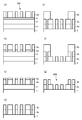
- FIG. 1 is a cross-sectional view showing a configuration of a mask blank 100 according to an embodiment of the present invention.
- a mask blank 100 of the present invention shown in FIG. 1 has a structure in which a phase shift film 2, a light shielding film 3, and a hard mask film 4 are laminated in this order on a translucent substrate 1.
- the phase shift film 2 is required to have a transmittance of 2% or more and less than 10% for exposure light (hereinafter referred to as ArF exposure light) having a wavelength of 200 nm or less, such as an ArF excimer laser.
- ArF exposure light exposure light
- the transmittance with respect to the exposure light is required to be at least 2%.
- the transmittance of the phase shift film 2 with respect to exposure light is preferably 3% or more, and more preferably 4% or more.
- the transmittance of the phase shift film 2 with respect to the exposure light increases, the calculation load of the bias (EMF bias) due to the electromagnetic field effect in the optical simulation performed at the time of mask pattern design tends to increase.
- the transmittance of the phase shift film 2 with respect to the exposure light is preferably less than 10%, more preferably 9% or less, and further preferably 8% or less.
- the phase shift film 2 has a phase difference of 150 between the transmitted ArF exposure light and the light that has passed through the air by the same distance as the thickness of the phase shift film 2. It is required to be adjusted to be in the range of not less than 90 degrees and not more than 190 degrees.
- the lower limit value of the phase difference in the phase shift film 2 is preferably 160 degrees or more, and more preferably 170 degrees or more.
- the upper limit value of the phase difference in the phase shift film 2 is preferably 180 degrees or less, and more preferably 179 degrees or less. This is to reduce the influence of an increase in phase difference caused by minute etching of the translucent substrate 1 during dry etching when forming a pattern on the phase shift film 2.
- ArF exposure light is applied to the phase shift mask by an exposure apparatus, and the number of ArF exposure light incident from a direction inclined at a predetermined angle with respect to the direction perpendicular to the film surface of the phase shift film 2 is increasing. It is because it is.
- the phase shift film 2 has a structure in which a lower layer 21 and an upper layer 22 are laminated from the translucent substrate 1 side.
- the lower layer 21 of the phase shift film 2 is formed of a material containing metal and silicon and substantially not containing oxygen.
- the lower layer 21 is provided for facilitating detection of the etching end point between the phase shift film 2 and the translucent substrate 1 when the EB defect is corrected. This layer also contributes to reducing the thickness.
- the lower layer 21 needs to be a material which does not contain oxygen substantially.
- the material which does not substantially contain oxygen is a material whose oxygen content in the material is at least 5 atomic% or less.
- the oxygen content of the material formed by the lower layer 21 is preferably 3 atomic% or less, and more preferably the detection lower limit value or less when composition analysis is performed by X-ray photoelectron spectroscopy or the like.
- the lower layer 21 is more preferably formed of a material made of metal and silicon, or a material made of metal, silicon and nitrogen, and more preferably made of a material made of metal and silicon.
- the metal element contained in the material forming the lower layer 21 is preferably a transition metal element.
- transition metal elements in this case molybdenum (Mo), tantalum (Ta), tungsten (W), titanium (Ti), chromium (Cr), hafnium (Hf), nickel (Ni), vanadium (V), zirconium
- Zr molybdenum
- Ta tantalum
- Ti tungsten
- Ti titanium
- Cr chromium
- Hf nickel
- zirconium One or more metal elements of (Zr), ruthenium (Ru), rhodium (Rh), zinc (Zn), niobium (Nb), and palladium (Pd) can be used.
- metal element other than the transition metal element contained in the material forming the lower layer 21 include aluminum (Al), indium (In), tin (Sn), and gallium (Ga).
- the material forming the lower layer 21 may contain elements such as carbon (C), hydrogen (H), boron (B), germanium (Ge), and antimony (Sb) in addition to the above-described elements.
- the material forming the lower layer 21 may include an inert gas such as helium (He), argon (Ar), krypton (Kr), and xenon (Xe).
- the nitrogen content is preferably 20 atomic% or less, more preferably 19 atomic% or more, and further preferably 15 atomic% or less.
- the nitrogen content of the material forming the lower layer 21 in this case is preferably 5 atomic% or more, and more preferably 10 atomic% or more.
- the upper layer 22 of the phase shift film 2 is formed of a material containing metal, silicon, nitrogen and oxygen. As described above, in order to reduce fluctuations in the transmittance and the phase shift amount of the phase shift film 2, it is necessary to contain oxygen when forming the upper layer 22. Considering these points, the oxygen content of the material formed by the upper layer 22 is preferably more than 5 atomic%, more preferably 10 atomic% or more, and further preferably 12 atomic% or more. Oxygen tends to decrease both the refractive index n and the extinction coefficient k of the material as the content in the material increases.
- the oxygen content of the material forming the upper layer 22 is preferably 30 atomic percent or less, more preferably 25 atomic percent or less, and further preferably 20 atomic percent or less.
- the nitrogen content of the material forming the upper layer 22 is preferably 20 atomic% or more, more preferably 25 atomic% or more, and further preferably 30 atomic% or more.
- the nitrogen content of the material formed by the upper layer 22 is preferably 50 atomic percent or less, more preferably 45 atomic percent or less, and even more preferably 40 atomic percent or less.
- the total content of nitrogen and oxygen in the upper layer 22 is required to be larger than the total content of nitrogen and oxygen in the lower layer 21.
- the difference obtained by subtracting the total content of nitrogen and oxygen in the lower layer 21 from the total content of nitrogen and oxygen in the upper layer 22 is preferably at least 10 atomic%, more preferably 15 atomic% or more, and more preferably 20 atomic%. More preferably, the above is true. Further, the difference obtained by subtracting the total content of nitrogen and oxygen in the lower layer 21 from the total content of nitrogen and oxygen in the upper layer 22 is preferably at least 60 atomic%, more preferably 55 atomic% or more, and 50 More preferably, it is at least atomic percent.
- the lower layer 21 is preferably formed in contact with the surface of the translucent substrate 1. This is because at the time of EB defect correction, it is preferable that there is no film of a material (for example, a chromium-based material film) difficult to correct the EB defect between the translucent substrate 1 and the lower layer 21. Moreover, since the lower layer 21 is provided in the phase shift film 2, even if the transparent substrate 1 and the lower layer 21 of the glass material are in contact with each other, the phase shift film 2 and the transparent substrate 1 are fixed at the time of EB defect correction. This is because the etching end point detection is relatively easy.
- a material for example, a chromium-based material film
- the M / [M + Si] ratio in the upper layer 22 is required to be smaller than the M / [M + Si] ratio in the lower layer 21.
- the upper layer 22 needs to suppress fluctuations in the transmittance and the phase shift amount, and the M / [M + Si] ratio is required to be small, whereas the lower layer 21 can easily detect the etching end point when correcting the EB defect. This is because the M / [M + Si] ratio is required to be large.
- the difference obtained by subtracting the M / [M + Si] ratio in the upper layer 22 from the M / [M + Si] ratio in the lower layer 21 is preferably at least 2% or more, more preferably 5% or more.
- the difference obtained by subtracting the M / [M + Si] ratio in the upper layer 22 from the M / [M + Si] ratio in the lower layer 21 is preferably at least 15% or less. If the difference in the M / [M + Si] ratio between the lower layer 21 and the upper layer 22 is greater than 15%, the difference in etching rate in the EB defect correction between the lower layer 21 and the upper layer 22 becomes large, and the EB defect correction. A step is likely to occur in the shape of the pattern side wall of the phase shift film 2 in the portion subjected to.
- the difference obtained by subtracting the M / [M + Si] ratio in the upper layer 22 from the M / [M + Si] ratio in the lower layer 21 is more preferably 10% or less, and further preferably 8% or less.
- the M / [M + Si] ratio in the material forming the lower layer 21 is required to be at least 8%, It is preferably 9% or more, and more preferably 10% or more.
- the M / [M + Si] ratio in the material forming the lower layer 21 is required to be at least 20% or less. If the M / [M + Si] ratio of the lower layer 21 is larger than 20%, the extinction coefficient k of the lower layer 21 increases, so that the transmittance for ArF exposure light in the entire phase shift film 2 is adjusted to a predetermined range. In addition, the thickness of the lower layer 21 needs to be significantly reduced.
- the M / [M + Si] ratio in the material forming the lower layer 21 is preferably 15% or less, and more preferably 12% or less.
- the material forming the upper layer 22 of the phase shift film 2 does not contain a metal element that contributes to increasing both the refractive index n and the extinction coefficient k, the total thickness of the phase shift film 2 is increased. Problems arise. In addition, when the upper layer 22 is formed by DC sputtering, there is a problem that defects due to the low conductivity of the metal silicide target increase. Considering these points, the M / [M + Si] ratio in the upper layer 22 is preferably 2% or more, and more preferably 3% or more.
- the M / [M + Si] ratio in the upper layer 22 is preferably 7% or less, and 6% or less. More preferably, it is more preferably 5% or less.
- Matters concerning metal elements contained in the material forming the upper layer 22, matters concerning metals other than transition metal elements contained in the material forming the upper layer 22, and matters concerning other elements contained in the material forming the upper layer 22 Is the same as in the case of the lower layer 21.
- Both the material forming the lower layer 21 and the material forming the upper layer 22 preferably contain the same metal element.
- the upper layer 22 and the lower layer 21 are patterned by dry etching using the same etching gas. For this reason, it is desirable to etch the upper layer 22 and the lower layer 21 in the same etching chamber. If the metal elements contained in the materials forming the upper layer 22 and the lower layer 21 are the same, it is possible to reduce environmental changes in the etching chamber when the object to be dry etched from the upper layer 22 to the lower layer 21 changes. it can.
- the phase shift film 2 is required to have a thickness of at least 90 nm. This is to reduce the bias (EMF bias) related to the electromagnetic field effect.
- the thickness of the phase shift film 2 is preferably 85 nm or less, and more preferably 80 nm or less. Further, the thickness of the phase shift film 2 is required to be 50 nm or more, preferably 55 nm or more, and more preferably 60 nm or more.
- the thickness of the lower layer 21 in the phase shift film 2 is required to be thinner than the thickness of the upper layer 22.
- the thickness of the lower layer 21 is preferably 1/3 or less of the total thickness of the phase shift film 2 and more preferably 1/5 or less. Further, the thickness of the lower layer 21 is preferably 1/30 or more of the total thickness of the phase shift film 2, more preferably 1/20 or more, and further preferably 1/15 or more.
- the lower layer 21 is required to have a thickness of 2 nm or more in order to exhibit a function of facilitating detection of an etching end point between the phase shift film 2 and the translucent substrate 1 when correcting the EB defect.
- the lower layer 21 is preferably 3 nm or more, and more preferably 5 nm or more.
- the lower layer 21 is required to have a thickness of 30 nm or less, preferably 25 nm or less, and more preferably 20 nm or less.
- the refractive index n of the lower layer 21 is preferably 1.00 or more, and more preferably 1.10 or more. Moreover, the refractive index n of the lower layer 21 is preferably 1.90 or less, and more preferably 1.70 or less.
- the extinction coefficient k of the lower layer 21 is preferably 2.40 or more, and more preferably 2.60 or more. Further, the extinction coefficient k of the lower layer 21 is preferably 3.30 or less, and more preferably 3.00 or less.
- the refractive index n of the upper layer 22 is preferably 2.00 or more, and more preferably 2.10 or more.
- the refractive index n of the upper layer 22 is preferably 2.65 or less, and more preferably 2.55 or less.
- the extinction coefficient k of the upper layer 22 is preferably 0.20 or more, and more preferably 0.30 or more.
- the extinction coefficient k of the upper layer 22 is preferably 0.60 or less, and more preferably 0.50 or less.
- the refractive index n and extinction coefficient k of the thin film including the phase shift film 2 are not determined only by the composition of the thin film.
- the film density and crystal state of the thin film are factors that influence the refractive index n and the extinction coefficient k. For this reason, various conditions when forming a thin film by reactive sputtering are adjusted, and the thin film is formed so as to have a desired refractive index n and extinction coefficient k.
- a mixture of a rare gas and a reactive gas oxygen gas, nitrogen gas, etc.
- the lower layer 21 and the upper layer 22 in the phase shift film 2 are formed by sputtering, but any sputtering such as DC sputtering, RF sputtering, and ion beam sputtering is applicable. In the case of using a target with low conductivity, it is preferable to apply RF sputtering or ion beam sputtering, but it is more preferable to apply RF sputtering in consideration of the film formation rate.
- the lower layer 21 and the upper layer 22 cannot be formed by the same single target. This is because the M / [M + Si] ratio of the lower layer 21 and the upper layer 22 is different.
- the lower layer 21 and the upper layer 22 may be formed with two targets having different M / [M + Si] ratios, they may be formed in the same film forming chamber or in different film forming chambers.
- the lower layer 21 and the upper layer 22 may be formed using a silicon target and a metal silicide target, and the lower layer 21 and the upper layer 22 having different M / [M + Si] ratios are formed by sputtering that changes a voltage applied to each target.
- the lower layer 21 and the upper layer 22 having different M / [M + Si] ratios may be formed by sputtering using a silicon target and a metal silicide target for the lower layer 21 and the upper layer 22 and changing the voltage applied to each target.
- the film forming chambers are connected to each other through, for example, different vacuum chambers.
- a transfer device robot hand for transferring the translucent substrate 1 between the load lock chamber, the vacuum chamber, and each film forming chamber.
- the upper layer 22 preferably has a layer having a higher oxygen content than the upper layer 22 excluding the surface layer (hereinafter simply referred to as a surface oxide layer).
- a surface oxide layer As a method of forming the surface oxide layer of the upper layer 22, various oxidation treatments can be applied. Examples of the oxidation treatment include a heat treatment in a gas containing oxygen such as the atmosphere, a light irradiation treatment using a flash lamp in a gas containing oxygen, a treatment in which ozone or oxygen plasma is brought into contact with the uppermost layer, and the like. can give.
- a surface oxide layer on the upper layer 22 is preferable to form a surface oxide layer on the upper layer 22 using a heat treatment that can simultaneously reduce the film stress of the phase shift film 2 or a light irradiation treatment using a flash lamp or the like.
- the surface oxide layer of the upper layer 22 preferably has a thickness of 1 nm or more, and more preferably 1.5 nm or more.
- the surface oxide layer of the upper layer 22 preferably has a thickness of 5 nm or less, more preferably 3 nm or less.
- the translucent substrate 1 can be formed of synthetic quartz glass, quartz glass, aluminosilicate glass, soda lime glass, low thermal expansion glass (SiO 2 —TiO 2 glass or the like) and the like.
- synthetic quartz glass has a high transmittance with respect to ArF excimer laser light, and is particularly preferable as a material for forming the translucent substrate 1 of the mask blank 100.
- the mask blank 100 includes a light shielding film 3 on the phase shift film 2.
- the outer peripheral region of a region where a transfer pattern is formed (transfer pattern forming region) is transmitted through the outer peripheral region when exposed and transferred to a resist film on a semiconductor wafer using an exposure device. It is required to secure an optical density (OD) of a predetermined value or higher so that the resist film is not affected by exposure light. This also applies to the phase shift mask.
- OD optical density
- the OD is 3.0 or more, and at least 2.8 or more is required.
- the phase shift film 2 has a function of transmitting exposure light with a predetermined transmittance, and it is difficult to ensure a predetermined optical density with the phase shift film 2 alone. For this reason, it is necessary to laminate the light shielding film 3 on the phase shift film 2 at the stage of manufacturing the mask blank 100 in order to ensure an insufficient optical density.
- the light shielding film 3 in the region (basically the transfer pattern forming region) where the phase shift effect is used is removed in the course of manufacturing the phase shift mask 200 (see FIG. 2). By doing so, it is possible to manufacture the phase shift mask 200 in which an optical density of a predetermined value is secured in the outer peripheral region.
- the light shielding film 3 can be applied to either a single layer structure or a laminated structure of two or more layers.
- each layer of the light shielding film having a single layer structure and the light shielding film having a laminated structure of two or more layers has a composition gradient in the thickness direction of the layer even if the layers have almost the same composition in the film thickness direction. It may be a configuration.
- the mask blank 100 in the form shown in FIG. 1 has a configuration in which the light shielding film 3 is laminated on the phase shift film 2 without interposing another film.
- the light-shielding film 3 is preferably formed of a material containing chromium.
- the material containing chromium forming the light-shielding film 3 include a material containing one or more elements selected from oxygen, nitrogen, carbon, boron, and fluorine in addition to chromium metal.
- a chromium-based material is etched with a mixed gas of a chlorine-based gas and an oxygen gas, but chromium metal does not have a high etching rate with respect to this etching gas.
- the material for forming the light shielding film 3 is one or more elements selected from chromium, oxygen, nitrogen, carbon, boron and fluorine. A material containing is preferred.
- the chromium-containing material forming the light-shielding film 3 may contain one or more elements of indium, molybdenum, and tin. By including one or more elements of indium, molybdenum and tin, the etching rate with respect to the mixed gas of chlorine-based gas and oxygen gas can be further increased.
- the present invention includes a configuration in which another film (etching stopper film) is interposed between the phase shift film 2 and the light shielding film 3 as the mask blank 100 of another embodiment.
- the etching stopper film is formed of the above-described material containing chromium
- the light-shielding film 3 is formed of a material containing silicon or a material containing tantalum.
- the material containing silicon forming the light shielding film 3 may contain a transition metal or a metal element other than the transition metal. This is because when the phase shift mask 200 is manufactured from the mask blank 100, the pattern formed by the light shielding film 3 is basically a light shielding band pattern in the outer peripheral region, and is irradiated with ArF exposure light as compared with the transfer pattern region. This is because it is rare that the integrated amount is small or the light shielding film 3 remains in a fine pattern, and even if the ArF light resistance is low, a substantial problem hardly occurs. In addition, when the light shielding film 3 contains a transition metal, the light shielding performance is greatly improved as compared with the case where no transition metal is contained, and the thickness of the light shielding film 3 can be reduced.
- the transition metal contained in the light shielding film 3 includes molybdenum (Mo), tantalum (Ta), tungsten (W), titanium (Ti), chromium (Cr), hafnium (Hf), nickel (Ni). , Vanadium (V), zirconium (Zr), ruthenium (Ru), rhodium (Rh), niobium (Nb), palladium (Pd), or any one metal or an alloy of these metals.
- the hard mask film 4 formed of a material having etching selectivity with respect to an etching gas used when the light shielding film 3 is etched is further laminated on the light shielding film 3. Since the light-shielding film 3 has a function of ensuring a predetermined optical density, there is a limit to reducing its thickness. It is sufficient for the hard mask film 4 to have a film thickness that can function as an etching mask until the dry etching for forming a pattern on the light shielding film 3 immediately below the hard mask film 4 is completed. Not subject to restrictions. For this reason, the thickness of the hard mask film 4 can be made much thinner than the thickness of the light shielding film 3.
- the resist film made of an organic material is sufficient to have a thickness sufficient to function as an etching mask until dry etching for forming a pattern on the hard mask film 4 is completed.
- the thickness can be greatly reduced. Thinning the resist film is effective in improving resist resolution and preventing pattern collapse, and is extremely important in meeting the demand for miniaturization.
- the hard mask film 4 is preferably formed of the material containing silicon. Since the hard mask film 4 in this case tends to have low adhesion to the organic material resist film, the surface of the hard mask film 4 is subjected to HMDS (Hexamethyldisilazane) treatment to improve surface adhesion. It is preferable. In this case, the hard mask film 4 is more preferably formed of SiO 2 , SiN, SiON or the like.
- a material containing tantalum is also applicable as the material of the hard mask film 4 when the light shielding film 3 is formed of a material containing chromium.
- the material containing tantalum in this case include a material in which tantalum contains one or more elements selected from nitrogen, oxygen, boron, and carbon in addition to tantalum metal. Examples thereof include Ta, TaN, TaO, TaON, TaBN, TaBO, TaBON, TaCN, TaCO, TaCON, TaBCN, TaBOCN, and the like.
- the hard mask film 4 is preferably formed of the material containing chromium.
- a resist film of an organic material is formed with a thickness of 100 nm or less in contact with the surface of the hard mask film 4.
- SRAF Sub-Resolution Assist Feature
- a transfer pattern phase shift pattern
- the phase shift mask 200 of this embodiment is characterized in that a transfer pattern (phase shift pattern 2a) is formed on the phase shift film 2 of the mask blank 100, and a pattern including a light shielding band pattern is formed on the light shielding film 3. Yes.
- a transfer pattern phase shift pattern 2a
- a pattern including a light shielding band pattern is formed on the light shielding film 3.
- the manufacturing method of the phase shift mask 200 uses the mask blank 100 described above.
- a step of forming a pattern is demonstrated.
- phase shift mask 200 using the mask blank 100 in which the hard mask film 4 is laminated on the light shielding film 3 will be described. Further, a material containing chromium is applied to the light shielding film 3, and a material containing silicon is applied to the hard mask film 4.
- a resist film is formed by spin coating in contact with the hard mask film 4 in the mask blank 100.
- a first pattern which is a transfer pattern (phase shift pattern) to be formed on the phase shift film 2
- a predetermined process such as a development process is further performed.
- a resist film (first resist pattern) 5a having a shift pattern was formed (see FIG. 2A).
- dry etching using a fluorine-based gas was performed using the first resist pattern 5a as a mask to form a first pattern (hard mask pattern 4a) on the hard mask film 4 (see FIG. 2B). .
- a resist film was formed on the mask blank 100 by a spin coating method.
- a second pattern which is a pattern (light-shielding pattern) to be formed on the light-shielding film 3
- a predetermined process such as a development process is performed to provide a light-shielding pattern.
- a second resist pattern 6b was formed (see FIG. 2E).
- dry etching using a mixed gas of chlorine-based gas and oxygen gas is performed using the second resist pattern 6b as a mask to form a second pattern (light-shielding pattern 3b) on the light-shielding film 3 (FIG. 3 ( f)).
- the second resist pattern 6b was removed, and a predetermined process such as cleaning was performed to obtain a phase shift mask 200 (see FIG. 3G).
- the chlorine-based gas used in the dry etching is not particularly limited as long as it contains Cl.
- Cl 2 , SiCl 2 , CHCl 3 , CH 2 Cl 2 , CCl 4 , BCl 3 and the like can be mentioned.
- the fluorine-based gas used in the dry etching is not particularly limited as long as F is contained.
- F for example, CHF 3, CF 4, C 2 F 6, C 4 F 8, SF 6 and the like.
- the fluorine-based gas not containing C has a relatively low etching rate with respect to the glass substrate, damage to the glass substrate can be further reduced.
- phase shift mask 200 of the present invention is manufactured using the mask blank 100 described above.
- the phase shift film 2 (phase shift pattern 2a) on which the transfer pattern is formed has a transmittance with respect to ArF exposure light of 2% or more and less than 10%, and the exposure light and the phase shift pattern transmitted through the phase shift pattern 2a.
- the phase difference between the exposure light passing through the air by the same distance as the thickness of 2a is in the range of 150 degrees to 190 degrees.
- the phase shift mask 200 of the present invention includes at least the phase shift pattern 2 a on the translucent substrate 1.
- the phase shift pattern 2a has a function of transmitting ArF excimer laser exposure light with a transmittance of 2% or more and less than 10%, and the same distance as the thickness of the phase shift pattern 2a with respect to the exposure light transmitted through the phase shift pattern 2a. And a function of causing a phase difference of 150 degrees or more and 190 degrees or less with the exposure light that has passed through the air.
- the phase shift pattern 2a includes a structure in which a lower layer 21 and an upper layer 22 are stacked from the translucent substrate 1 side.
- the lower layer 21 is made of a material containing metal and silicon and substantially free of oxygen
- the upper layer 22 is made of a material containing metal, silicon, nitrogen and oxygen.
- the thickness of the lower layer 21 is smaller than the thickness of the upper layer 22, and the ratio of the metal content to the total content of metal and silicon in the upper layer 22 is the ratio of the metal to the total content of the metal and silicon in the lower layer 21. It is smaller than the content ratio.
- the phase shift mask 200 of the present invention may include a light shielding pattern 3b including a light shielding band pattern on the phase shift pattern 2a.
- the phase shift mask 200 of the present invention is generated by the further progress of the elution of the metal element from the phase shift pattern 2a and the oxidation of the surface layer, even though the phase shift pattern 2a is formed of a material containing metal and silicon. It is possible to reduce changes in transmittance and phase shift amount with respect to exposure light. In addition, the etching end point can be detected relatively easily when the EB defect is corrected for the black defect of the phase shift pattern 2a discovered by the mask inspection performed in the process of manufacturing the phase shift mask 200.
- the semiconductor device manufacturing method of the present invention uses the phase shift mask 200 manufactured using the phase shift mask 200 or the mask blank 100 to expose and transfer a pattern onto a resist film on a semiconductor substrate. It is said. Therefore, the change in optical characteristics of the phase shift mask 200 before and after the mask cleaning is small, and even if exposure transfer is performed on the resist film on the semiconductor device using the phase shift mask 200 after the mask cleaning, The pattern can be transferred to the resist film with sufficient accuracy to meet the design specifications. Further, even when the black defect portion is exposed and transferred to the resist film on the semiconductor device using the phase shift mask 200 in which the black defect portion is corrected by the EB defect correction in the course of the production, the black defect of the phase shift mask 200 exists.
- Example 1 Manufacture of mask blanks
- a translucent substrate 1 made of synthetic quartz glass having a main surface dimension of about 152 mm ⁇ about 152 mm and a thickness of about 6.35 mm was prepared.
- the translucent substrate 1 had its end face and main surface polished to a predetermined surface roughness and then subjected to a predetermined cleaning process and drying process.
- DC sputtering reactive sputtering
- a mixed gas of (Ar) and helium (He) is sputtered
- a lower layer 21 (MoSi film) of the phase shift film 2 made of molybdenum and silicon is formed on the translucent substrate 1 by 7 nm. The thickness was formed.
- the upper layer 22 (MoSiON film) made of silicon, nitrogen and oxygen was formed to a thickness of 72 nm.
- a heat treatment for reducing the film stress of the phase shift film 2 and forming an oxide layer on the surface layer was performed on the translucent substrate 1 on which the phase shift film 2 was formed. Specifically, using a heating furnace (electric furnace), heat treatment was performed in the atmosphere at a heating temperature of 450 ° C. and a heating time of 1 hour. A phase shift film 2 in which a lower layer 21 and an upper layer 22 were laminated under the same conditions on the main surface of another translucent substrate 1 and heat-treated was prepared. Using a phase shift amount measuring apparatus (MPM193, manufactured by Lasertec Corporation), the transmittance and phase difference of the phase shift film 2 with respect to light having a wavelength of 193 nm were measured. The transmittance was 6.1% and the phase difference was 171.1. Degree.
- phase shift film 2 was analyzed by STEM and EDX, it was confirmed that an oxide layer was formed with a thickness of about 1.5 nm from the surface of the upper layer 22 of the phase shift film 2. .
- the lower layer 21 had a refractive index n of 1.16 and an extinction coefficient k of 2.91, and the upper layer 22 had a refractive index.
- n was 2.38 and the extinction coefficient k was 0.32.
- the surface reflectance of the phase shift film 2 (reflectance on the surface side of the phase shift film 2) was 20.6%
- the back surface reflectance (reflectance on the side of the translucent substrate 1) was 36.2%. .
- the lowermost layer of the light shielding film 3 made of CrOCN was formed to a thickness of 30 nm on the phase shift film 2 by reactive sputtering (DC sputtering).
- Ar argon
- N 2 nitrogen
- the lower layer of the light shielding film 3 made of CrN was formed to a thickness of 4 nm on the lowermost layer of the light shielding film 3 by reactive sputtering (DC sputtering).
- the upper layer of 3 was formed with a thickness of 14 nm.
- the light-shielding film 3 made of a chromium-based material having a three-layer structure of the lowermost layer made of CrOCN, the lower layer made of CrN, and the upper layer made of CrOCN was formed with a total film thickness of 48 nm from the phase shift film 2 side.
- the optical density (OD) at a wavelength of 193 nm in the laminated structure of the phase shift film 2 and the light shielding film 3 was measured and found to be 3.0 or more.
- the translucent substrate 1 in which the phase shift film 2 and the light-shielding film 3 are laminated is installed in a single wafer RF sputtering apparatus, and a silicon dioxide (SiO 2 ) target is used and argon (Ar) gas is sputtered. Then, a hard mask film 4 made of silicon and oxygen was formed to a thickness of 5 nm on the light shielding film 3 by RF sputtering.
- a mask blank 100 having a structure in which a phase shift film 2 having a two-layer structure, a light shielding film 3 and a hard mask film 4 were laminated on a translucent substrate 1 was manufactured.
- phase shift mask 200 of Example 1 was produced according to the following procedure. First, the surface of the hard mask film 4 was subjected to HMDS treatment. Subsequently, a resist film made of a chemically amplified resist for electron beam drawing with a film thickness of 80 nm was formed in contact with the surface of the hard mask film 4 by spin coating. Next, a first pattern which is a phase shift pattern to be formed on the phase shift film 2 is drawn on the resist film by electron beam, a predetermined development process and a cleaning process are performed, and a first pattern having the first pattern is obtained. 1 resist pattern 5a was formed (see FIG. 2A). At this time, a program defect was added to the first pattern drawn by the electron beam in addition to the phase shift pattern to be originally formed so that a black defect was formed in the phase shift film 2.
- the first resist pattern 5a was removed.
- dry etching using fluorine-based gas SF 6 + He is performed to form a first pattern (phase shift pattern 2a) on the phase shift film 2, and at the same time, a hard mask pattern 4a was removed (see FIG. 2 (d)).
- a resist film made of a chemically amplified resist for electron beam lithography was formed on the light-shielding pattern 3a with a film thickness of 150 nm by spin coating.
- a second pattern which is a pattern (light-shielding pattern) to be formed on the light-shielding film 3, is exposed and drawn on the resist film, and a predetermined process such as a development process is further performed to provide a second pattern having a light-shielding pattern.
- a resist pattern 6b was formed (see FIG. 2E).
- Example 2 Manufacture of mask blanks
- the mask blank 100 of Example 2 was manufactured in the same procedure as in Example 1 except for the phase shift film 2.
- the material for forming the lower layer 21 is changed, and the film thicknesses of the lower layer 21 and the upper layer 22 are changed.
- Mo molybdenum
- Si silicon
- DC sputtering reactive sputtering
- a mixed gas of argon (Ar), nitrogen (N 2 ), and helium (He) is sputtered.
- Two lower layers 21 (MoSiN film) were formed to a thickness of 7.7 nm.
- the upper layer 22 (MoSiON film) made of silicon, nitrogen and oxygen was formed to a thickness of 71.0 nm.
- Example 2 the heat treatment was performed on the phase shift film 2 of Example 2 under the same processing conditions as in Example 1.
- a phase shift film 2 of Example 2 was formed on the main surface of another translucent substrate 1 under the same conditions, and a heat treatment was prepared.
- a phase shift amount measuring device MPM193, manufactured by Lasertec Corporation
- the transmittance and phase difference of the phase shift film 2 with respect to light having a wavelength of 193 nm were measured.
- the transmittance was 6.13% and the phase difference was 170.5. Degree.
- this phase shift film 2 was analyzed by STEM and EDX, it was confirmed that an oxide layer was formed with a thickness of about 1.5 nm from the surface of the upper layer 22 of the phase shift film 2. .
- the lower layer 21 had a refractive index n of 1.20 and an extinction coefficient k of 2.78
- the upper layer 22 had a refractive index.
- n was 2.38 and the extinction coefficient k was 0.32.
- the mask blank of Example 2 having a structure in which the phase shift film 2, the light-shielding film 3, and the hard mask film 4 composed of the lower layer 21 of MoSiN and the upper layer 22 of MoSiON are laminated on the translucent substrate 1 by the above procedure. 100 was produced.
- Example 3 Manufacture of mask blanks
- the mask blank 100 of Example 3 was manufactured in the same procedure as Example 1 except for the phase shift film 2.
- the material forming the lower layer 21 is changed, and the film thicknesses of the lower layer 21 and the upper layer 22 are changed.
- Mo molybdenum
- Si silicon
- DC sputtering reactive sputtering
- a mixed gas of argon (Ar), nitrogen (N 2 ), and helium (He) is sputtered.
- Two lower layers 21 (MoSiN film) were formed to a thickness of 4.5 nm.
- the upper layer 22 (MoSiON film) made of silicon, nitrogen and oxygen was formed to a thickness of 72.1 nm.
- Example 3 the heat treatment was performed on the phase shift film 2 of Example 3 under the same processing conditions as in Example 1.
- a phase shift film 2 of Example 2 was formed on the main surface of another translucent substrate 1 under the same conditions, and a heat treatment was prepared.
- a phase shift amount measuring device MPM193, manufactured by Lasertec Corporation
- the transmittance and phase difference of the phase shift film 2 with respect to light having a wavelength of 193 nm were measured.
- the transmittance was 6.08% and the phase difference was 170.2. Degree.
- this phase shift film 2 was analyzed by STEM and EDX, it was confirmed that an oxide layer was formed with a thickness of about 1.5 nm from the surface of the upper layer 22 of the phase shift film 2. .
- the lower layer 21 had a refractive index n of 1.52, an extinction coefficient k of 2.73, and the upper layer 22 had a refractive index.
- n was 2.38 and the extinction coefficient k was 0.32.
- the mask blank of Example 3 having a structure in which the phase shift film 2, the light-shielding film 3, and the hard mask film 4 composed of the lower layer 21 of MoSiN and the upper layer 22 of MoSiON are laminated on the translucent substrate 1 by the above procedure. 100 was produced.
- phase shift mask 200 of Example 3 was produced in the same procedure as in Example 1.
- Comparative Example 1 Manufacture of mask blanks
- the mask blank of Comparative Example 1 was manufactured in the same procedure as in Example 1 except for the phase shift film 2.
- the phase shift film 2 of Comparative Example 1 a film having a single layer structure made of molybdenum, silicon, nitrogen and oxygen was applied.
- phase shift film 2 was formed with a thickness of 66 nm.
- phase shift film 2 was also subjected to heat treatment under the same processing conditions as in Example 1.
- a phase shift film 2 of Comparative Example 1 was formed on the main surface of another translucent substrate 1 under the same conditions, and a heat treatment was prepared.
- a phase shift amount measuring device MPM193, manufactured by Lasertec Corporation
- the transmittance and phase difference of the phase shift film 2 with respect to light having a wavelength of 193 nm were measured.
- the transmittance was 12.1% and the phase difference was 177.1. Degree.
- the phase shift film 2 was analyzed by STEM and EDX, it was confirmed that an oxide layer was formed with a thickness of about 1.7 nm from the surface of the phase shift film 2.
- the refractive index n was 2.48 and the extinction coefficient k was 0.45.
- a mask blank of Comparative Example 1 having a structure in which a phase shift film 2 made of MoSiON, a light shielding film 3 and a hard mask film 4 were laminated on a translucent substrate 1 was manufactured.
Landscapes
- Chemical & Material Sciences (AREA)
- Engineering & Computer Science (AREA)
- Metallurgy (AREA)
- Organic Chemistry (AREA)
- Chemical Kinetics & Catalysis (AREA)
- Materials Engineering (AREA)
- Mechanical Engineering (AREA)
- Physics & Mathematics (AREA)
- General Physics & Mathematics (AREA)
- Power Engineering (AREA)
- Condensed Matter Physics & Semiconductors (AREA)
- Manufacturing & Machinery (AREA)
- Computer Hardware Design (AREA)
- Microelectronics & Electronic Packaging (AREA)
- Inorganic Chemistry (AREA)
- Thermal Sciences (AREA)
- Health & Medical Sciences (AREA)
- Environmental & Geological Engineering (AREA)
- Epidemiology (AREA)
- Public Health (AREA)
- Preparing Plates And Mask In Photomechanical Process (AREA)
Abstract
Priority Applications (5)
| Application Number | Priority Date | Filing Date | Title |
|---|---|---|---|
| JP2016507706A JP5940755B1 (ja) | 2014-12-26 | 2015-10-07 | マスクブランク、位相シフトマスク、位相シフトマスクの製造方法および半導体デバイスの製造方法 |
| US15/503,415 US10146123B2 (en) | 2014-12-26 | 2015-10-07 | Mask blank, phase shift mask, method for manufacturing phase shift mask, and method for manufacturing semiconductor device |
| KR1020167016865A KR101810805B1 (ko) | 2014-12-26 | 2015-10-07 | 마스크 블랭크, 위상 시프트 마스크, 위상 시프트 마스크의 제조 방법 및 반도체 디바이스의 제조 방법 |
| KR1020177009289A KR102261621B1 (ko) | 2014-12-26 | 2015-10-07 | 마스크 블랭크, 위상 시프트 마스크, 위상 시프트 마스크의 제조 방법 및 반도체 디바이스의 제조 방법 |
| US16/175,035 US10551734B2 (en) | 2014-12-26 | 2018-10-30 | Mask blank, phase shift mask, method for manufacturing phase shift mask, and method for manufacturing semiconductor device |
Applications Claiming Priority (2)
| Application Number | Priority Date | Filing Date | Title |
|---|---|---|---|
| JP2014-265189 | 2014-12-26 | ||
| JP2014265189 | 2014-12-26 |
Related Child Applications (2)
| Application Number | Title | Priority Date | Filing Date |
|---|---|---|---|
| US15/503,415 A-371-Of-International US10146123B2 (en) | 2014-12-26 | 2015-10-07 | Mask blank, phase shift mask, method for manufacturing phase shift mask, and method for manufacturing semiconductor device |
| US16/175,035 Division US10551734B2 (en) | 2014-12-26 | 2018-10-30 | Mask blank, phase shift mask, method for manufacturing phase shift mask, and method for manufacturing semiconductor device |
Publications (1)
| Publication Number | Publication Date |
|---|---|
| WO2016103843A1 true WO2016103843A1 (fr) | 2016-06-30 |
Family
ID=56149880
Family Applications (1)
| Application Number | Title | Priority Date | Filing Date |
|---|---|---|---|
| PCT/JP2015/078471 WO2016103843A1 (fr) | 2014-12-26 | 2015-10-07 | Ébauche de masque, masque à déphasage, procédé de fabrication d'un masque à déphasage et procédé de fabrication d'un dispositif à semi-conducteur |
Country Status (5)
| Country | Link |
|---|---|
| US (2) | US10146123B2 (fr) |
| JP (2) | JP5940755B1 (fr) |
| KR (2) | KR101810805B1 (fr) |
| TW (2) | TWI648592B (fr) |
| WO (1) | WO2016103843A1 (fr) |
Cited By (6)
| Publication number | Priority date | Publication date | Assignee | Title |
|---|---|---|---|---|
| WO2017010452A1 (fr) * | 2015-07-15 | 2017-01-19 | Hoya株式会社 | Ébauche de masque, masque à déphasage, procédé de production de masque à déphasage et procédé de production de dispositif à semi-conducteurs |
| JP2017037278A (ja) * | 2015-08-14 | 2017-02-16 | Hoya株式会社 | マスクブランク、位相シフトマスクおよび半導体デバイスの製造方法 |
| WO2017057376A1 (fr) * | 2015-09-30 | 2017-04-06 | Hoya株式会社 | Ébauche de masque, masque à décalage de phase, et procédé de production de dispositif semi-conducteur |
| JP2018077418A (ja) * | 2016-11-11 | 2018-05-17 | Hoya株式会社 | マスクブランク、転写用マスク、転写用マスクの製造方法および半導体デバイスの製造方法 |
| CN108663896A (zh) * | 2017-03-28 | 2018-10-16 | Hoya株式会社 | 相移掩模坯料及使用其的相移掩模的制造方法、以及图案转印方法 |
| WO2019188397A1 (fr) * | 2018-03-26 | 2019-10-03 | Hoya株式会社 | Ébauche de masque, masque à déphasage, et procédé de fabrication de dispositif à semi-conducteur |
Families Citing this family (13)
| Publication number | Priority date | Publication date | Assignee | Title |
|---|---|---|---|---|
| TW201823855A (zh) * | 2016-09-21 | 2018-07-01 | 日商Hoya股份有限公司 | 光罩之製造方法、光罩、及顯示裝置之製造方法 |
| JP6891099B2 (ja) * | 2017-01-16 | 2021-06-18 | Hoya株式会社 | 位相シフトマスクブランクおよびこれを用いた位相シフトマスクの製造方法、並びに表示装置の製造方法 |
| JP6791031B2 (ja) * | 2017-06-13 | 2020-11-25 | 信越化学工業株式会社 | フォトマスクブランク及びその製造方法 |
| WO2018230233A1 (fr) * | 2017-06-14 | 2018-12-20 | Hoya株式会社 | Ébauche de masque, masque de déphasage et procédé de production de dispositif à semi-conducteur |
| JP6729508B2 (ja) * | 2017-06-29 | 2020-07-22 | 信越化学工業株式会社 | フォトマスクブランク及びフォトマスク |
| JP6753375B2 (ja) * | 2017-07-28 | 2020-09-09 | 信越化学工業株式会社 | フォトマスクブランク、フォトマスクブランクの製造方法及びフォトマスクの製造方法 |
| EP3486721A1 (fr) | 2017-11-17 | 2019-05-22 | IMEC vzw | Masque pour la lithographie à ultraviolets extrêmes et son procédé de fabrication |
| JP6557381B1 (ja) * | 2018-05-08 | 2019-08-07 | エスアンドエス テック カンパニー リミテッド | 位相反転ブランクマスク及びフォトマスク |
| KR20210014619A (ko) | 2018-05-25 | 2021-02-09 | 호야 가부시키가이샤 | 반사형 마스크 블랭크, 반사형 마스크 및 그 제조 방법, 그리고 반도체 장치의 제조 방법 |
| JP6938428B2 (ja) * | 2018-05-30 | 2021-09-22 | Hoya株式会社 | マスクブランク、位相シフトマスクおよび半導体デバイスの製造方法 |
| EP4066276A4 (fr) * | 2019-11-27 | 2024-03-27 | Corning Inc | Tranches de verre pour fabriquer des dispositifs à semi-conducteurs |
| CN113064300A (zh) * | 2021-03-26 | 2021-07-02 | 绵阳惠科光电科技有限公司 | 一种彩膜基板、彩膜基板的制作方法及液晶显示面板 |
| JP7375065B2 (ja) * | 2022-02-24 | 2023-11-07 | Hoya株式会社 | マスクブランク、転写用マスクの製造方法、及び表示装置の製造方法 |
Citations (5)
| Publication number | Priority date | Publication date | Assignee | Title |
|---|---|---|---|---|
| JP2003005347A (ja) * | 2001-06-26 | 2003-01-08 | Shin Etsu Chem Co Ltd | 位相シフトマスクブランク及びその製造方法 |
| JP2007241136A (ja) * | 2006-03-10 | 2007-09-20 | Toppan Printing Co Ltd | クロムレス位相シフトマスク用フォトマスクブランク、クロムレス位相シフトマスク、及びクロムレス位相シフトマスクの製造方法 |
| JP2011112824A (ja) * | 2009-11-26 | 2011-06-09 | Hoya Corp | マスクブランク及び転写用マスク並びにそれらの製造方法 |
| JP2013231952A (ja) * | 2012-04-30 | 2013-11-14 | S&S Tech Corp | 位相反転ブランクマスク及びその製造方法 |
| JP2014145920A (ja) * | 2013-01-29 | 2014-08-14 | Hoya Corp | マスクブランク、転写用マスク、マスクブランクの製造方法、転写用マスクの製造方法、および半導体デバイスの製造方法 |
Family Cites Families (17)
| Publication number | Priority date | Publication date | Assignee | Title |
|---|---|---|---|---|
| JP5215421B2 (ja) * | 1999-11-09 | 2013-06-19 | アルバック成膜株式会社 | 位相シフトフォトマスクブランクス及び位相シフトフォトマスク並びに半導体装置の製造方法 |
| JP2001201842A (ja) | 1999-11-09 | 2001-07-27 | Ulvac Seimaku Kk | 位相シフトフォトマスクブランクス及び位相シフトフォトマスク並びに半導体装置の製造方法 |
| US6645677B1 (en) | 2000-09-18 | 2003-11-11 | Micronic Laser Systems Ab | Dual layer reticle blank and manufacturing process |
| JP3818171B2 (ja) | 2002-02-22 | 2006-09-06 | Hoya株式会社 | 位相シフトマスクブランク及びその製造方法 |
| JP2002258458A (ja) | 2000-12-26 | 2002-09-11 | Hoya Corp | ハーフトーン型位相シフトマスク及びマスクブランク |
| JP2004537758A (ja) | 2001-07-27 | 2004-12-16 | エフ・イ−・アイ・カンパニー | 電子ビーム処理 |
| KR100815679B1 (ko) * | 2001-11-27 | 2008-03-20 | 호야 가부시키가이샤 | 하프톤형 위상 시프트 마스크 블랭크, 하프톤형 위상시프트 마스크 및 그 제조방법 |
| DE10307518B4 (de) | 2002-02-22 | 2011-04-14 | Hoya Corp. | Halbtonphasenschiebermaskenrohling, Halbtonphasenschiebermaske und Verfahren zu deren Herstellung |
| JP4525893B2 (ja) | 2003-10-24 | 2010-08-18 | 信越化学工業株式会社 | 位相シフトマスクブランク、位相シフトマスク及びパターン転写方法 |
| TWI480675B (zh) | 2004-03-31 | 2015-04-11 | Shinetsu Chemical Co | 半色調相移空白光罩,半色調相移光罩,以及圖案轉移方法 |
| JP4348536B2 (ja) | 2004-03-31 | 2009-10-21 | 信越化学工業株式会社 | 位相シフトマスクブランク、位相シフトマスク及びパターン転写方法 |
| JP5165833B2 (ja) * | 2005-02-04 | 2013-03-21 | 信越化学工業株式会社 | フォトマスクブランク、フォトマスク、およびフォトマスクブランクの製造方法 |
| JP5507860B2 (ja) | 2009-02-12 | 2014-05-28 | Hoya株式会社 | フォトマスクの製造方法 |
| JP2010217514A (ja) | 2009-03-17 | 2010-09-30 | Toppan Printing Co Ltd | フォトマスクの製造方法 |
| CN110673435B (zh) | 2013-01-15 | 2023-04-21 | Hoya株式会社 | 掩膜板坯料、相移掩膜板及半导体器件的制造方法 |
| JP6005530B2 (ja) * | 2013-01-15 | 2016-10-12 | Hoya株式会社 | マスクブランク、位相シフトマスクおよびこれらの製造方法 |
| JP6373607B2 (ja) * | 2013-03-08 | 2018-08-15 | Hoya株式会社 | マスクブランクの製造方法および位相シフトマスクの製造方法 |
-
2015
- 2015-10-07 WO PCT/JP2015/078471 patent/WO2016103843A1/fr active Application Filing
- 2015-10-07 KR KR1020167016865A patent/KR101810805B1/ko active IP Right Grant
- 2015-10-07 KR KR1020177009289A patent/KR102261621B1/ko active IP Right Grant
- 2015-10-07 JP JP2016507706A patent/JP5940755B1/ja active Active
- 2015-10-07 US US15/503,415 patent/US10146123B2/en active Active
- 2015-11-03 TW TW106107539A patent/TWI648592B/zh active
- 2015-11-03 TW TW104136205A patent/TWI584056B/zh active
-
2016
- 2016-05-13 JP JP2016096881A patent/JP6599281B2/ja active Active
-
2018
- 2018-10-30 US US16/175,035 patent/US10551734B2/en active Active
Patent Citations (5)
| Publication number | Priority date | Publication date | Assignee | Title |
|---|---|---|---|---|
| JP2003005347A (ja) * | 2001-06-26 | 2003-01-08 | Shin Etsu Chem Co Ltd | 位相シフトマスクブランク及びその製造方法 |
| JP2007241136A (ja) * | 2006-03-10 | 2007-09-20 | Toppan Printing Co Ltd | クロムレス位相シフトマスク用フォトマスクブランク、クロムレス位相シフトマスク、及びクロムレス位相シフトマスクの製造方法 |
| JP2011112824A (ja) * | 2009-11-26 | 2011-06-09 | Hoya Corp | マスクブランク及び転写用マスク並びにそれらの製造方法 |
| JP2013231952A (ja) * | 2012-04-30 | 2013-11-14 | S&S Tech Corp | 位相反転ブランクマスク及びその製造方法 |
| JP2014145920A (ja) * | 2013-01-29 | 2014-08-14 | Hoya Corp | マスクブランク、転写用マスク、マスクブランクの製造方法、転写用マスクの製造方法、および半導体デバイスの製造方法 |
Cited By (14)
| Publication number | Priority date | Publication date | Assignee | Title |
|---|---|---|---|---|
| US10935881B2 (en) | 2015-07-15 | 2021-03-02 | Hoya Corporation | Mask blank, phase shift mask, phase shift mask manufacturing method, and semiconductor device manufacturing method |
| WO2017010452A1 (fr) * | 2015-07-15 | 2017-01-19 | Hoya株式会社 | Ébauche de masque, masque à déphasage, procédé de production de masque à déphasage et procédé de production de dispositif à semi-conducteurs |
| US10114281B2 (en) | 2015-08-14 | 2018-10-30 | Hoya Corporation | Mask blank, phase shift mask, and method for manufacturing semiconductor device |
| JP2017037278A (ja) * | 2015-08-14 | 2017-02-16 | Hoya株式会社 | マスクブランク、位相シフトマスクおよび半導体デバイスの製造方法 |
| WO2017029981A1 (fr) * | 2015-08-14 | 2017-02-23 | Hoya株式会社 | Ébauche de masque, masque à décalage de phase, et procédé de fabrication de dispositif à semi-conducteurs |
| US10606164B2 (en) | 2015-08-14 | 2020-03-31 | Hoya Corporation | Mask blank, phase shift mask, and method for manufacturing semiconductor device |
| US10481486B2 (en) | 2015-09-30 | 2019-11-19 | Hoya Corporation | Mask blank, phase shift mask, and method for manufacturing semiconductor device |
| JP6133530B1 (ja) * | 2015-09-30 | 2017-05-24 | Hoya株式会社 | マスクブランク、位相シフトマスクおよび半導体デバイスの製造方法 |
| WO2017057376A1 (fr) * | 2015-09-30 | 2017-04-06 | Hoya株式会社 | Ébauche de masque, masque à décalage de phase, et procédé de production de dispositif semi-conducteur |
| US10942441B2 (en) | 2015-09-30 | 2021-03-09 | Hoya Corporation | Mask blank, phase shift mask, and method for manufacturing semiconductor device |
| JP2018077418A (ja) * | 2016-11-11 | 2018-05-17 | Hoya株式会社 | マスクブランク、転写用マスク、転写用マスクの製造方法および半導体デバイスの製造方法 |
| CN108663896A (zh) * | 2017-03-28 | 2018-10-16 | Hoya株式会社 | 相移掩模坯料及使用其的相移掩模的制造方法、以及图案转印方法 |
| CN108663896B (zh) * | 2017-03-28 | 2023-11-28 | Hoya株式会社 | 相移掩模坯料、相移掩模的制造方法、以及图案转印方法 |
| WO2019188397A1 (fr) * | 2018-03-26 | 2019-10-03 | Hoya株式会社 | Ébauche de masque, masque à déphasage, et procédé de fabrication de dispositif à semi-conducteur |
Also Published As
| Publication number | Publication date |
|---|---|
| US20190064651A1 (en) | 2019-02-28 |
| TW201719270A (zh) | 2017-06-01 |
| JP2016164683A (ja) | 2016-09-08 |
| JPWO2016103843A1 (ja) | 2017-04-27 |
| KR102261621B1 (ko) | 2021-06-04 |
| KR101810805B1 (ko) | 2017-12-19 |
| US10551734B2 (en) | 2020-02-04 |
| JP5940755B1 (ja) | 2016-06-29 |
| TW201624104A (zh) | 2016-07-01 |
| KR20170089836A (ko) | 2017-08-04 |
| TWI584056B (zh) | 2017-05-21 |
| KR20160094999A (ko) | 2016-08-10 |
| TWI648592B (zh) | 2019-01-21 |
| US10146123B2 (en) | 2018-12-04 |
| US20170285458A1 (en) | 2017-10-05 |
| JP6599281B2 (ja) | 2019-10-30 |
Similar Documents
| Publication | Publication Date | Title |
|---|---|---|
| JP6599281B2 (ja) | マスクブランク、位相シフトマスク、位相シフトマスクの製造方法および半導体デバイスの製造方法 | |
| JP6297734B2 (ja) | マスクブランク、位相シフトマスクおよび半導体デバイスの製造方法 | |
| JP6153894B2 (ja) | マスクブランク、位相シフトマスク、位相シフトマスクの製造方法及び半導体デバイスの製造方法 | |
| WO2017010452A1 (fr) | Ébauche de masque, masque à déphasage, procédé de production de masque à déphasage et procédé de production de dispositif à semi-conducteurs | |
| JP6430666B2 (ja) | マスクブランク、位相シフトマスク、位相シフトマスクの製造方法及び半導体デバイスの製造方法 | |
| JP6545795B2 (ja) | マスクブランク、転写用マスク、マスクブランクの製造方法、転写用マスクの製造方法および半導体デバイスの製造方法 | |
| JP6430155B2 (ja) | マスクブランク、位相シフトマスク、位相シフトマスクの製造方法および半導体デバイスの製造方法 | |
| JP6720139B2 (ja) | マスクブランク、位相シフトマスク、位相シフトマスクの製造方法および半導体デバイスの製造方法 | |
| JP6321265B2 (ja) | マスクブランク、位相シフトマスク、位相シフトマスクの製造方法及び半導体デバイスの製造方法 | |
| JP2016186535A (ja) | マスクブランク、位相シフトマスク、位相シフトマスクの製造方法および半導体デバイスの製造方法 | |
| WO2019188397A1 (fr) | Ébauche de masque, masque à déphasage, et procédé de fabrication de dispositif à semi-conducteur | |
| JP6740349B2 (ja) | マスクブランク、位相シフトマスク、及び半導体デバイスの製造方法 | |
| KR20210056343A (ko) | 마스크 블랭크, 전사용 마스크 및 반도체 디바이스의 제조 방법 | |
| JP2018132686A (ja) | マスクブランク、転写用マスク、転写用マスクの製造方法および半導体デバイスの製造方法 |
Legal Events
| Date | Code | Title | Description |
|---|---|---|---|
| ENP | Entry into the national phase |
Ref document number: 2016507706 Country of ref document: JP Kind code of ref document: A |
|
| ENP | Entry into the national phase |
Ref document number: 20167016865 Country of ref document: KR Kind code of ref document: A |
|
| 121 | Ep: the epo has been informed by wipo that ep was designated in this application |
Ref document number: 15872412 Country of ref document: EP Kind code of ref document: A1 |
|
| WWE | Wipo information: entry into national phase |
Ref document number: 15503415 Country of ref document: US |
|
| NENP | Non-entry into the national phase |
Ref country code: DE |
|
| 122 | Ep: pct application non-entry in european phase |
Ref document number: 15872412 Country of ref document: EP Kind code of ref document: A1 |