WO2016084533A1 - マイクロ流路作製用原盤、転写物、およびマイクロ流路作製用原盤の製造方法 - Google Patents
マイクロ流路作製用原盤、転写物、およびマイクロ流路作製用原盤の製造方法 Download PDFInfo
- Publication number
- WO2016084533A1 WO2016084533A1 PCT/JP2015/080104 JP2015080104W WO2016084533A1 WO 2016084533 A1 WO2016084533 A1 WO 2016084533A1 JP 2015080104 W JP2015080104 W JP 2015080104W WO 2016084533 A1 WO2016084533 A1 WO 2016084533A1
- Authority
- WO
- WIPO (PCT)
- Prior art keywords
- main
- concavo
- fine
- convex portion
- master
- Prior art date
- Legal status (The legal status is an assumption and is not a legal conclusion. Google has not performed a legal analysis and makes no representation as to the accuracy of the status listed.)
- Ceased
Links
Images






Classifications
-
- B—PERFORMING OPERATIONS; TRANSPORTING
- B01—PHYSICAL OR CHEMICAL PROCESSES OR APPARATUS IN GENERAL
- B01L—CHEMICAL OR PHYSICAL LABORATORY APPARATUS FOR GENERAL USE
- B01L3/00—Containers or dishes for laboratory use, e.g. laboratory glassware; Droppers
- B01L3/50—Containers for the purpose of retaining a material to be analysed, e.g. test tubes
- B01L3/502—Containers for the purpose of retaining a material to be analysed, e.g. test tubes with fluid transport, e.g. in multi-compartment structures
- B01L3/5027—Containers for the purpose of retaining a material to be analysed, e.g. test tubes with fluid transport, e.g. in multi-compartment structures by integrated microfluidic structures, i.e. dimensions of channels and chambers are such that surface tension forces are important, e.g. lab-on-a-chip
- B01L3/502707—Containers for the purpose of retaining a material to be analysed, e.g. test tubes with fluid transport, e.g. in multi-compartment structures by integrated microfluidic structures, i.e. dimensions of channels and chambers are such that surface tension forces are important, e.g. lab-on-a-chip characterised by the manufacture of the container or its components
-
- B—PERFORMING OPERATIONS; TRANSPORTING
- B01—PHYSICAL OR CHEMICAL PROCESSES OR APPARATUS IN GENERAL
- B01J—CHEMICAL OR PHYSICAL PROCESSES, e.g. CATALYSIS OR COLLOID CHEMISTRY; THEIR RELEVANT APPARATUS
- B01J19/00—Chemical, physical or physico-chemical processes in general; Their relevant apparatus
-
- B—PERFORMING OPERATIONS; TRANSPORTING
- B01—PHYSICAL OR CHEMICAL PROCESSES OR APPARATUS IN GENERAL
- B01J—CHEMICAL OR PHYSICAL PROCESSES, e.g. CATALYSIS OR COLLOID CHEMISTRY; THEIR RELEVANT APPARATUS
- B01J19/00—Chemical, physical or physico-chemical processes in general; Their relevant apparatus
- B01J19/0093—Microreactors, e.g. miniaturised or microfabricated reactors
-
- B—PERFORMING OPERATIONS; TRANSPORTING
- B01—PHYSICAL OR CHEMICAL PROCESSES OR APPARATUS IN GENERAL
- B01L—CHEMICAL OR PHYSICAL LABORATORY APPARATUS FOR GENERAL USE
- B01L3/00—Containers or dishes for laboratory use, e.g. laboratory glassware; Droppers
- B01L3/50—Containers for the purpose of retaining a material to be analysed, e.g. test tubes
- B01L3/502—Containers for the purpose of retaining a material to be analysed, e.g. test tubes with fluid transport, e.g. in multi-compartment structures
- B01L3/5027—Containers for the purpose of retaining a material to be analysed, e.g. test tubes with fluid transport, e.g. in multi-compartment structures by integrated microfluidic structures, i.e. dimensions of channels and chambers are such that surface tension forces are important, e.g. lab-on-a-chip
- B01L3/50273—Containers for the purpose of retaining a material to be analysed, e.g. test tubes with fluid transport, e.g. in multi-compartment structures by integrated microfluidic structures, i.e. dimensions of channels and chambers are such that surface tension forces are important, e.g. lab-on-a-chip characterised by the means or forces applied to move the fluids
-
- B—PERFORMING OPERATIONS; TRANSPORTING
- B01—PHYSICAL OR CHEMICAL PROCESSES OR APPARATUS IN GENERAL
- B01L—CHEMICAL OR PHYSICAL LABORATORY APPARATUS FOR GENERAL USE
- B01L3/00—Containers or dishes for laboratory use, e.g. laboratory glassware; Droppers
- B01L3/50—Containers for the purpose of retaining a material to be analysed, e.g. test tubes
- B01L3/502—Containers for the purpose of retaining a material to be analysed, e.g. test tubes with fluid transport, e.g. in multi-compartment structures
- B01L3/5027—Containers for the purpose of retaining a material to be analysed, e.g. test tubes with fluid transport, e.g. in multi-compartment structures by integrated microfluidic structures, i.e. dimensions of channels and chambers are such that surface tension forces are important, e.g. lab-on-a-chip
- B01L3/502746—Containers for the purpose of retaining a material to be analysed, e.g. test tubes with fluid transport, e.g. in multi-compartment structures by integrated microfluidic structures, i.e. dimensions of channels and chambers are such that surface tension forces are important, e.g. lab-on-a-chip characterised by the means for controlling flow resistance, e.g. flow controllers, baffles or throttle valves
-
- B—PERFORMING OPERATIONS; TRANSPORTING
- B29—WORKING OF PLASTICS; WORKING OF SUBSTANCES IN A PLASTIC STATE IN GENERAL
- B29C—SHAPING OR JOINING OF PLASTICS; SHAPING OF MATERIAL IN A PLASTIC STATE, NOT OTHERWISE PROVIDED FOR; AFTER-TREATMENT OF THE SHAPED PRODUCTS, e.g. REPAIRING
- B29C33/00—Moulds or cores; Details thereof or accessories therefor
- B29C33/38—Moulds or cores; Details thereof or accessories therefor characterised by the material or the manufacturing process
-
- B—PERFORMING OPERATIONS; TRANSPORTING
- B29—WORKING OF PLASTICS; WORKING OF SUBSTANCES IN A PLASTIC STATE IN GENERAL
- B29C—SHAPING OR JOINING OF PLASTICS; SHAPING OF MATERIAL IN A PLASTIC STATE, NOT OTHERWISE PROVIDED FOR; AFTER-TREATMENT OF THE SHAPED PRODUCTS, e.g. REPAIRING
- B29C33/00—Moulds or cores; Details thereof or accessories therefor
- B29C33/38—Moulds or cores; Details thereof or accessories therefor characterised by the material or the manufacturing process
- B29C33/3842—Manufacturing moulds, e.g. shaping the mould surface by machining
-
- B—PERFORMING OPERATIONS; TRANSPORTING
- B29—WORKING OF PLASTICS; WORKING OF SUBSTANCES IN A PLASTIC STATE IN GENERAL
- B29C—SHAPING OR JOINING OF PLASTICS; SHAPING OF MATERIAL IN A PLASTIC STATE, NOT OTHERWISE PROVIDED FOR; AFTER-TREATMENT OF THE SHAPED PRODUCTS, e.g. REPAIRING
- B29C33/00—Moulds or cores; Details thereof or accessories therefor
- B29C33/42—Moulds or cores; Details thereof or accessories therefor characterised by the shape of the moulding surface, e.g. ribs or grooves
-
- B—PERFORMING OPERATIONS; TRANSPORTING
- B29—WORKING OF PLASTICS; WORKING OF SUBSTANCES IN A PLASTIC STATE IN GENERAL
- B29C—SHAPING OR JOINING OF PLASTICS; SHAPING OF MATERIAL IN A PLASTIC STATE, NOT OTHERWISE PROVIDED FOR; AFTER-TREATMENT OF THE SHAPED PRODUCTS, e.g. REPAIRING
- B29C35/00—Heating, cooling or curing, e.g. crosslinking or vulcanising; Apparatus therefor
- B29C35/02—Heating or curing, e.g. crosslinking or vulcanizing during moulding, e.g. in a mould
- B29C35/08—Heating or curing, e.g. crosslinking or vulcanizing during moulding, e.g. in a mould by wave energy or particle radiation
- B29C35/0805—Heating or curing, e.g. crosslinking or vulcanizing during moulding, e.g. in a mould by wave energy or particle radiation using electromagnetic radiation
-
- B—PERFORMING OPERATIONS; TRANSPORTING
- B29—WORKING OF PLASTICS; WORKING OF SUBSTANCES IN A PLASTIC STATE IN GENERAL
- B29C—SHAPING OR JOINING OF PLASTICS; SHAPING OF MATERIAL IN A PLASTIC STATE, NOT OTHERWISE PROVIDED FOR; AFTER-TREATMENT OF THE SHAPED PRODUCTS, e.g. REPAIRING
- B29C59/00—Surface shaping of articles, e.g. embossing; Apparatus therefor
- B29C59/02—Surface shaping of articles, e.g. embossing; Apparatus therefor by mechanical means, e.g. pressing
- B29C59/022—Surface shaping of articles, e.g. embossing; Apparatus therefor by mechanical means, e.g. pressing characterised by the disposition or the configuration, e.g. dimensions, of the embossments or the shaping tools therefor
-
- B—PERFORMING OPERATIONS; TRANSPORTING
- B81—MICROSTRUCTURAL TECHNOLOGY
- B81B—MICROSTRUCTURAL DEVICES OR SYSTEMS, e.g. MICROMECHANICAL DEVICES
- B81B1/00—Devices without movable or flexible elements, e.g. microcapillary devices
-
- B—PERFORMING OPERATIONS; TRANSPORTING
- B81—MICROSTRUCTURAL TECHNOLOGY
- B81C—PROCESSES OR APPARATUS SPECIALLY ADAPTED FOR THE MANUFACTURE OR TREATMENT OF MICROSTRUCTURAL DEVICES OR SYSTEMS
- B81C99/00—Subject matter not provided for in other groups of this subclass
-
- B—PERFORMING OPERATIONS; TRANSPORTING
- B81—MICROSTRUCTURAL TECHNOLOGY
- B81C—PROCESSES OR APPARATUS SPECIALLY ADAPTED FOR THE MANUFACTURE OR TREATMENT OF MICROSTRUCTURAL DEVICES OR SYSTEMS
- B81C99/00—Subject matter not provided for in other groups of this subclass
- B81C99/0075—Manufacture of substrate-free structures
- B81C99/0085—Manufacture of substrate-free structures using moulds and master templates, e.g. for hot-embossing
-
- B—PERFORMING OPERATIONS; TRANSPORTING
- B81—MICROSTRUCTURAL TECHNOLOGY
- B81C—PROCESSES OR APPARATUS SPECIALLY ADAPTED FOR THE MANUFACTURE OR TREATMENT OF MICROSTRUCTURAL DEVICES OR SYSTEMS
- B81C99/00—Subject matter not provided for in other groups of this subclass
- B81C99/0075—Manufacture of substrate-free structures
- B81C99/009—Manufacturing the stamps or the moulds
-
- G—PHYSICS
- G01—MEASURING; TESTING
- G01N—INVESTIGATING OR ANALYSING MATERIALS BY DETERMINING THEIR CHEMICAL OR PHYSICAL PROPERTIES
- G01N37/00—Details not covered by any other group of this subclass
-
- G—PHYSICS
- G03—PHOTOGRAPHY; CINEMATOGRAPHY; ANALOGOUS TECHNIQUES USING WAVES OTHER THAN OPTICAL WAVES; ELECTROGRAPHY; HOLOGRAPHY
- G03F—PHOTOMECHANICAL PRODUCTION OF TEXTURED OR PATTERNED SURFACES, e.g. FOR PRINTING, FOR PROCESSING OF SEMICONDUCTOR DEVICES; MATERIALS THEREFOR; ORIGINALS THEREFOR; APPARATUS SPECIALLY ADAPTED THEREFOR
- G03F7/00—Photomechanical, e.g. photolithographic, production of textured or patterned surfaces, e.g. printing surfaces; Materials therefor, e.g. comprising photoresists; Apparatus specially adapted therefor
- G03F7/0002—Lithographic processes using patterning methods other than those involving the exposure to radiation, e.g. by stamping
-
- B—PERFORMING OPERATIONS; TRANSPORTING
- B01—PHYSICAL OR CHEMICAL PROCESSES OR APPARATUS IN GENERAL
- B01J—CHEMICAL OR PHYSICAL PROCESSES, e.g. CATALYSIS OR COLLOID CHEMISTRY; THEIR RELEVANT APPARATUS
- B01J2219/00—Chemical, physical or physico-chemical processes in general; Their relevant apparatus
- B01J2219/00781—Aspects relating to microreactors
- B01J2219/00783—Laminate assemblies, i.e. the reactor comprising a stack of plates
- B01J2219/00786—Geometry of the plates
-
- B—PERFORMING OPERATIONS; TRANSPORTING
- B01—PHYSICAL OR CHEMICAL PROCESSES OR APPARATUS IN GENERAL
- B01J—CHEMICAL OR PHYSICAL PROCESSES, e.g. CATALYSIS OR COLLOID CHEMISTRY; THEIR RELEVANT APPARATUS
- B01J2219/00—Chemical, physical or physico-chemical processes in general; Their relevant apparatus
- B01J2219/00781—Aspects relating to microreactors
- B01J2219/00819—Materials of construction
- B01J2219/00833—Plastic
-
- B—PERFORMING OPERATIONS; TRANSPORTING
- B01—PHYSICAL OR CHEMICAL PROCESSES OR APPARATUS IN GENERAL
- B01J—CHEMICAL OR PHYSICAL PROCESSES, e.g. CATALYSIS OR COLLOID CHEMISTRY; THEIR RELEVANT APPARATUS
- B01J2219/00—Chemical, physical or physico-chemical processes in general; Their relevant apparatus
- B01J2219/00781—Aspects relating to microreactors
- B01J2219/00851—Additional features
- B01J2219/00855—Surface features
-
- B—PERFORMING OPERATIONS; TRANSPORTING
- B01—PHYSICAL OR CHEMICAL PROCESSES OR APPARATUS IN GENERAL
- B01L—CHEMICAL OR PHYSICAL LABORATORY APPARATUS FOR GENERAL USE
- B01L2200/00—Solutions for specific problems relating to chemical or physical laboratory apparatus
- B01L2200/12—Specific details about manufacturing devices
-
- B—PERFORMING OPERATIONS; TRANSPORTING
- B01—PHYSICAL OR CHEMICAL PROCESSES OR APPARATUS IN GENERAL
- B01L—CHEMICAL OR PHYSICAL LABORATORY APPARATUS FOR GENERAL USE
- B01L2300/00—Additional constructional details
- B01L2300/08—Geometry, shape and general structure
- B01L2300/0848—Specific forms of parts of containers
- B01L2300/0851—Bottom walls
-
- B—PERFORMING OPERATIONS; TRANSPORTING
- B01—PHYSICAL OR CHEMICAL PROCESSES OR APPARATUS IN GENERAL
- B01L—CHEMICAL OR PHYSICAL LABORATORY APPARATUS FOR GENERAL USE
- B01L2300/00—Additional constructional details
- B01L2300/16—Surface properties and coatings
- B01L2300/161—Control and use of surface tension forces, e.g. hydrophobic, hydrophilic
-
- B—PERFORMING OPERATIONS; TRANSPORTING
- B01—PHYSICAL OR CHEMICAL PROCESSES OR APPARATUS IN GENERAL
- B01L—CHEMICAL OR PHYSICAL LABORATORY APPARATUS FOR GENERAL USE
- B01L2400/00—Moving or stopping fluids
- B01L2400/08—Regulating or influencing the flow resistance
- B01L2400/084—Passive control of flow resistance
- B01L2400/088—Passive control of flow resistance by specific surface properties
-
- B—PERFORMING OPERATIONS; TRANSPORTING
- B29—WORKING OF PLASTICS; WORKING OF SUBSTANCES IN A PLASTIC STATE IN GENERAL
- B29C—SHAPING OR JOINING OF PLASTICS; SHAPING OF MATERIAL IN A PLASTIC STATE, NOT OTHERWISE PROVIDED FOR; AFTER-TREATMENT OF THE SHAPED PRODUCTS, e.g. REPAIRING
- B29C35/00—Heating, cooling or curing, e.g. crosslinking or vulcanising; Apparatus therefor
- B29C35/02—Heating or curing, e.g. crosslinking or vulcanizing during moulding, e.g. in a mould
- B29C35/08—Heating or curing, e.g. crosslinking or vulcanizing during moulding, e.g. in a mould by wave energy or particle radiation
- B29C35/0805—Heating or curing, e.g. crosslinking or vulcanizing during moulding, e.g. in a mould by wave energy or particle radiation using electromagnetic radiation
- B29C2035/0827—Heating or curing, e.g. crosslinking or vulcanizing during moulding, e.g. in a mould by wave energy or particle radiation using electromagnetic radiation using UV radiation
-
- B—PERFORMING OPERATIONS; TRANSPORTING
- B29—WORKING OF PLASTICS; WORKING OF SUBSTANCES IN A PLASTIC STATE IN GENERAL
- B29C—SHAPING OR JOINING OF PLASTICS; SHAPING OF MATERIAL IN A PLASTIC STATE, NOT OTHERWISE PROVIDED FOR; AFTER-TREATMENT OF THE SHAPED PRODUCTS, e.g. REPAIRING
- B29C59/00—Surface shaping of articles, e.g. embossing; Apparatus therefor
- B29C59/02—Surface shaping of articles, e.g. embossing; Apparatus therefor by mechanical means, e.g. pressing
- B29C59/022—Surface shaping of articles, e.g. embossing; Apparatus therefor by mechanical means, e.g. pressing characterised by the disposition or the configuration, e.g. dimensions, of the embossments or the shaping tools therefor
- B29C2059/023—Microembossing
Definitions
- the present invention relates to a microchannel manufacturing master, a transcript, and a method for manufacturing a microchannel manufacturing master.
- microfluidic chips have been developed in which wells and microchannels for chemical and biological analysis are provided on a resin or glass substrate.
- Patent Document 1 discloses a microfluidic chip in which the hydrophilicity of the surface of the microchannel is increased by irradiating a microchannel made of PMMA (polymethyl methacrylate) with a femtosecond laser. Yes.
- Patent Document 2 the surface of the microchannel made of silicone rubber is subjected to plasma modification treatment in a gas atmosphere containing nitrogen and amine, thereby improving the hydrophilicity of the surface of the microchannel.
- a fluidic chip is disclosed.
- Patent Document 3 discloses a method for producing a mold for producing a microfluidic chip.
- a microfluidic chip is manufactured by performing nanoimprint transfer using this template.
- Patent Documents 1 and 2 a microfluidic chip having a highly hydrophilic microchannel is obtained by performing the above treatment.
- the methods described in Patent Documents 1 and 2 are not preferable methods from the viewpoint of mass productivity.
- the material of a microchannel will be limited to PMMA and silicone rubber. .
- an object of the present invention is a novel and improved technique capable of easily mass-producing a transcript having a highly hydrophilic region.
- Another object of the present invention is to provide a microchannel manufacturing master, a transcript, and a method of manufacturing the microchannel manufacturing master.
- a base material a base material, a main concavo-convex portion provided on a surface of the base material and extending in a surface direction of the base material, and a surface of the main concavo-convex portion are provided.
- a master for producing a microchannel having a surface area ratio is provided.
- the main uneven portion may have a width and depth of 1 ⁇ m to 2000 ⁇ m, and the fine uneven portion may have a width and depth of 30 nm to 1000 nm.
- a plurality of the fine irregularities may be provided, and the width and depth of the fine irregularities may be different values for each position where the fine irregularities are formed.
- the fine uneven portion may be provided so as to extend along a longitudinal direction of the main uneven portion.
- a main concavo-convex portion extending in the surface direction of the base material is formed on the surface of the base material, and 10 pico is formed on the surface of the main concavo-convex portion.
- a master for producing a micro flow path which includes forming a fine uneven portion having a narrower pitch than the main uneven portion on the surface of the main uneven portion by irradiating an ultrashort pulse laser having a pulse width of less than a second.
- a manufacturing method is provided.
- the irradiation with the ultrashort pulse laser may be performed such that the polarization direction is orthogonal to the longitudinal direction of the main concavo-convex portion.
- a transfer product including a resin layer onto which the surface shape of the master plate for producing a microchannel is transferred.
- the main uneven portion may have a width and depth of 1 ⁇ m to 2000 ⁇ m, and the fine uneven portion may have a width and depth of 30 nm to 1000 nm.
- a plurality of the fine irregularities may be provided, and the width and depth of the fine irregularities may be different values for each position where the fine irregularities are formed.
- the fine uneven portion may be provided so as to extend along a longitudinal direction of the main uneven portion.
- the resin layer may be made of a curable hydrophilic resin.
- a microfluidic chip including the transcript is provided.
- FIG. 4 is a diagram illustrating an example of a polarization direction of an ultrashort pulse laser, a scanning direction, and a planar shape of a fine uneven portion 14 in a manufacturing process of the master 1.
- the master 1 is a master for producing a microchannel, and is used for imprint transfer including a roll-to-roll method. That is, the transferred product 5 is manufactured by transferring the concavo-convex shape provided on the surface of the master 1.
- the transfer product 5 is obtained by imprint transfer using the master 1, the surface of the transfer 5 is formed with unevenness that is a reverse of the uneven shape provided on the surface of the master 1. It will be. A concave portion formed on the surface of the transfer product 5 becomes a microchannel.
- the master 1 may be used not only when the transfer product 5 as a product such as a microfluidic chip is manufactured, but also when the replica master is manufactured by the imprint transfer method.
- the replica master has irregularities formed by inverting the irregularities provided on the surface of the master 1, and further, imprint transfer is performed using the replica master, whereby a transfer product 5 as a product can be manufactured. .
- FIG. 1 is a diagram schematically showing a cross section when the master 1 according to the present embodiment is cut in the thickness direction.
- the master 1 As shown in FIG. 1, the master 1 according to the present embodiment is provided on a flat substrate 10, a surface layer 16 laminated on the substrate 10, a surface of the surface layer 16, and the substrate 10. Compared with the main concavo-convex portion 11, the plurality of main concavo-convex portions 11 extending in the surface direction, the coating layer 15 covering the surfaces of the plurality of main concavo-convex portions 11, and the coating layer 15 on the surface of the plurality of main concavo-convex portions 11. And a plurality of fine irregularities 14 having a narrow pitch (period). Note that the master 1 may not include the surface layer 16, and in this case, the main concavo-convex portion 11 is directly provided on the surface of the substrate 10. Further, the master 1 may not include the covering layer 15, and in this case, the fine uneven portion 14 is directly provided on the surface of the surface layer 16.
- the substrate 10 is not limited to a flat plate shape as shown in FIG. 1, and may be a cylindrical shape or a columnar shape.
- the surface layer 16 and the main concavo-convex portion 11 are provided on the outer peripheral surface of the base material 10.
- the cylindrical or columnar master 1 can be used in a roll-to-roll imprint transfer method.
- the material of the base material 10 is not particularly limited, and metals such as stainless steel, Cu, Al, Ni, quartz glass (SiO 2 ) such as fused silica glass or synthetic quartz glass, semiconductor material, resin, and the like Can be used. Alternatively, a stacked material in which these materials are stacked may be used.
- the material of the surface layer 16 is not particularly limited, and a metal such as NiP, Ni, Cu, Al, or a laminated material thereof can be used.
- the thickness of the surface layer 16 is not particularly limited, but may be, for example, 50 ⁇ m to 300 ⁇ m.
- the material of the coating layer 15 is not particularly limited, and a metal such as Cu, Cr, Ni, NiP, and Al, or a carbon material such as diamond-like carbon (DLC) can be used.
- the thickness of the coating layer 15 is not particularly limited, but may be, for example, 0.1 ⁇ m to 300 ⁇ m.
- the main concavo-convex portion 11 is provided on the surface of the surface layer 16 or the surface of the base material 10, extends in the surface direction of the base material 10, and has a convex portion 12 and a concave portion 13. Specifically, one main concavo-convex part 11 has one convex part 12 and one concave part 13.
- the cross-sectional shape of the convex portion 12 is not limited to the shape shown in FIG. 1 and can be various shapes as will be described below.
- the cross-sectional shape of the convex part 12 means the contour shape of the surface of the convex part 12 in the cross section of the base material 10.
- the other cross-sectional shape of the convex part 12 is demonstrated using FIG. FIG.
- FIG. 2 is a diagram schematically showing a cross section of the convex portion 12 when the master 1 according to this embodiment is cut in the thickness direction.
- FIG. 2A is an example of the rectangular convex portion 12.
- FIG. 2B is an example of the trapezoidal convex portion 12 whose upper base is shorter than the lower base.
- FIG. 2C shows an example of a triangular convex portion 12 having a vertex located on the upper side.
- FIG. 2D is an example of the semicircular convex portion 12 in which an arc is located on the upper side. Further, FIG.
- the cross-sectional shape of the convex portion 12 may be a polygon such as a triangle or a quadrangle, the corner portion of the polygon may be a curve, or a curve such as a circle or an ellipse.
- the cross-sectional shape of the concave portion 13 forming a pair of the convex portions 12 is not limited to the shape as shown in FIG. 1 as in the cross-sectional shape of the convex portion 12, and may be various shapes. it can.
- the planar shape of the main concavo-convex portion 11 is not particularly limited, and can be various shapes.
- the planar shape of the main concavo-convex portion 11 refers to the shape of the main concavo-convex portion 11 when the surface of the base 10 is viewed from above the surface of the base 10, that is, the shape in a plan view.
- the planar shape of the main concavo-convex portion 11 will be described with reference to FIG.
- FIG. 3 is a diagram schematically showing a planar shape of the main concavo-convex portion 11 according to the present embodiment.
- FIG. 3A is an example of a linear main concavo-convex portion 11 extending in the surface direction of the substrate 10.
- FIG. 3B is an example of a curved main uneven portion 11.
- FIG. 3C is an example of the main concavo-convex portion 11 having a bent shape so as to form an obtuse angle in the surface direction of the substrate 10. That is, the planar shape of the main concavo-convex portion 11 according to the present embodiment is not particularly limited, and may be a straight shape or a curved shape, or may be a bent shape or a branched shape.
- the width and depth of the main concavo-convex portion 11 are not particularly limited, and may be, for example, 1 ⁇ m to 2000 ⁇ m.
- the width and depth of the main concavo-convex portion 11 are the width and depth (height) of the convex portion 12 and the concave portion 13.
- the width of the convex portion 12 refers to the width of the bottom portion of the convex portion 12 in the cross section when the master 1 is cut in a direction perpendicular to the longitudinal direction of the main concave and convex portion 11, and the width of the concave portion 13 is It refers to the width of the bottom surface of the recess 13 in the same cross section.
- the depth (height) of the convex portion refers to the length from the bottom portion to the upper end portion (upper end surface) in the same cross section, and the depth of the concave portion refers to the bottom portion to the upper end portion (opening surface) in the same cross section.
- Refers to the length of The convex portion 12 or the concave portion 13 may have a uniform width in one convex portion 12 or the concave portion 13, or may have a different width for each position in the one convex portion 12 or the concave portion 13.
- one fine uneven portion 14 has one fine convex portion 17 and one fine concave portion 18.
- the fine uneven portion 14 is provided on the upper surface of the convex portion 12 and the bottom surface of the concave portion 13.
- corrugated part 14 is not restricted to being provided in both the upper surface of the convex part 12, and the bottom face of the recessed part 13, and may be provided in any one.
- the fine concavo-convex portion 14 is provided on the upper surface of the convex portion 12.
- the width and depth of the fine uneven portion 14 are not particularly limited, but may be, for example, 30 nm to 1000 nm.
- the width and depth of the fine uneven portion 14 are the width and depth (height) of the fine convex portion 17 and the fine concave portion 18.
- the definition of the width and depth of the fine convex part 17 and the width and depth of the fine concave part 18 are the same as the definition of the convex part 12 and the concave part 13 described above.
- the width and depth of the fine uneven portions 14 may be different values for each position where the fine uneven portions 14 are formed.
- the surface of the main uneven part 11 provided with the fine uneven part 14 has an arithmetic average roughness (Ra) of 10 nm to 150 nm.
- the arithmetic average roughness can be obtained as follows.
- the shape in a 3 ⁇ m square region of the surface of the main concavo-convex portion 11 is measured with an atomic force microscope (AFM), and the arithmetic average roughness Ra is calculated according to JISB0601-2001.
- the surface of the main uneven portion 11 provided with the fine uneven portion 14 has a specific surface area ratio of 1.1 to 3.0.
- the specific surface area ratio can be obtained as follows. A region of 3 ⁇ m square on the surface of the main concavo-convex portion 11 is observed by AFM, and the measured surface area Sa of the surface is measured. The measured surface area Sa relative to the surface area Sm when Sa and the surface are ideal flat surfaces (mirror surfaces). Can be obtained by calculating the ratio.
- the formation direction of the fine concavo-convex portion 14 is not particularly limited, and can be various directions as described below.
- the formation direction of the fine irregularities 14 refers to the longitudinal direction of the fine irregularities 14 when the surface of the substrate 10 is viewed from above the surface of the substrate 10.
- the fine uneven portion 14 shown in FIG. 3A is provided so as to extend linearly along the longitudinal direction of the linear main uneven portion 11.
- the formation direction of the fine uneven portion 14 is a direction along the longitudinal direction of the main uneven portion 11.
- 3B and 3C are provided so as to extend along the longitudinal direction of the main concavo-convex portion 11 having a curved shape or a bent shape. In these cases, the fine concavo-convex portion 14 shown in FIG.
- FIG. 4 is a diagram schematically showing another planar shape of the main concavo-convex portion 11 according to the present embodiment.
- FIG. 4A is an example of the fine concavo-convex portion 14 having a forming direction along the longitudinal direction of the linear main concavo-convex portion 11, as in FIG. 3A.
- FIG. 4B is an example of the fine concavo-convex portion 14 when the formation direction of the fine concavo-convex portion 14 is orthogonal to the longitudinal direction of the linear main concavo-convex portion 11.
- FIG. 4C is an example of the fine uneven portion 14 in the case where the formation direction of the fine uneven portion 14 is inclined with respect to the longitudinal direction of the linear main uneven portion 11.
- planar shape of the fine concavo-convex portion 14 is not limited to a linear shape as in the examples described so far, and can be various shapes.
- the fine irregularities 14 may be dot-like or mesh-like.
- the fine uneven portion 14 may have a different formation direction and shape for each position in the main uneven portion 11.
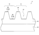
- FIG. 5 is a view schematically showing a cross section when the transfer product 5 according to the present embodiment is cut in the thickness direction.
- the transfer product 5 includes a resin layer 55 to which the surface shape of the master 1 according to the present embodiment is transferred.
- the transfer product 5 includes a flat substrate 50, a resin layer 55 provided on the surface of the substrate 50, and main irregularities provided on the surface of the resin layer 55 and extending in the surface direction of the resin layer 55.
- Part 51 and a fine uneven part 54 provided on the surface of the main uneven part 51 and having a narrower pitch than the main uneven part 51.
- the material of the base material 50 is not particularly limited, and resin, quartz glass such as fused silica glass or synthetic quartz glass, semiconductor material, or metal such as stainless steel can be used. Alternatively, a stacked material in which these materials are stacked may be used. In addition, as a material of the base material 50, the material with high adhesiveness with the resin layer 55 demonstrated later is preferable.
- the size of the base material 50 is not particularly limited as long as the base material of the transfer material 5 having a microchannel generally has a size.
- the curable hydrophilic resin 56 which is a composition of the resin layer 55 is a hydrophilic resin having a curable type of either a photo-curable type or a thermosetting type. Furthermore, the resin layer 55 is preferably a photo-curing hydrophilic resin 56 that is a resin that decreases in fluidity and is cured when irradiated with light having a predetermined wavelength.
- the photocurable hydrophilic resin 56 is an ultraviolet curable resin such as an acrylic resin acrylate.
- the curable hydrophilic resin 56 may contain an initiator, a filler, a functional additive, a solvent, an inorganic material, a pigment, an antistatic agent, a sensitizing dye, or the like, as necessary.
- the thickness of the resin layer 55 is not particularly limited, but may be, for example, 0.1 ⁇ m to 300 ⁇ m.
- the main concavo-convex portion 51 is provided on the surface of the resin layer 55, extends in the surface direction of the resin layer 55, and has a convex portion 52 and a concave portion 53. Specifically, one main concavo-convex portion 51 has one convex portion 52 and one concave portion 53.
- the cross-sectional shape of the concave portion 53 constituting the main concave / convex portion 51 is not limited to the shape shown in FIG. 5, and has a shape in which the cross-sectional shape of the convex portion 12 of the master 1 is reversed. Various shapes can be used according to the cross-sectional shape of the convex portion 12.
- the cross-sectional shape of the recessed part 53 means the outline shape of the space in the recessed part 53 in the cross section of the transcription
- FIG. the cross-sectional shape of the convex portion 52 forming a pair of the concave portions 53 can be various shapes according to the cross-sectional shape of the concave portion 13 of the master 1.
- the planar shape and the forming direction of the main concavo-convex portion 51 are not particularly limited, and the plane shape of the main concavo-convex portion 11 of the master 1 has a transferred shape. Various shapes and forming directions can be used according to the shape.
- the main concavo-convex portion 51 has a reversed shape of the main concavo-convex portion 11 of the master 1. Therefore, the width and depth (height) of the main uneven portion 51 are the same values as the width and depth (height) of the main uneven portion 11 of the master 1.
- the definition of the width and depth of the main uneven portion 51 is the same as the definition of the width and height of the main uneven portion 11.
- the width and depth of the convex portion 52 and the concave portion 53 may be, for example, 1 ⁇ m to 2000 ⁇ m according to the main concave and convex portion 11 of the master 1.
- the plurality of main concavo-convex parts 51 preferably have the same width as each other, similarly to the main concavo-convex part 11 of the master 1, and are formed on the base material 50 at the same pitch (period) along the surface direction of the base material 50. Preferably it is formed.
- the size of the pitch may be 1 ⁇ m to 2000 ⁇ m, for example, according to the main concavo-convex portion 11 of the master 1.
- the fine concavo-convex portion 54 is provided on the surface of the main concavo-convex portion 51, has a fine convex portion 57 and a fine concave portion 58, and has a narrower pitch (period) than the main concavo-convex portion 51.
- one fine uneven portion 54 has one fine convex portion 57 and one fine concave portion 58.
- the fine uneven portion 54 is formed by transferring the shape of the fine uneven portion 14 of the master 1, the fine uneven portion 54 has a cross-sectional shape in which the cross-sectional shape of the fine uneven portion 14 of the master 1 is reversed.
- the planar shape of one fine concavo-convex portion 14 has a planar shape that is a transferred shape.
- the fine uneven portion 54 is provided on the upper surface of the convex portion 52 and the bottom surface of the concave portion 53.
- corrugated part 54 is not restricted to being provided in both the upper surface of the convex part 52, and the bottom face of the recessed part 53, You may provide in any one.
- the fine uneven portion 54 is provided on the bottom surface of the recessed portion 53.
- the fine concavo-convex portion 54 has an inverted shape of the fine concavo-convex portion 14 of the master 1. Therefore, the width and depth (height) of the fine irregularities 54 are the same values as the width and depth (height) of the fine irregularities 14 of the master 1.
- the definition of the width and depth of the fine uneven portion 54 is the same as the definition of the width and height of the fine uneven portion 14.
- the width and depth of the fine convex portion 57 and the fine concave portion 58 may be 30 nm to 1000 nm.
- the width and depth of the fine uneven portions 54 can be different values for each position where the fine uneven portions 54 are formed.
- the surface of the main uneven part 51 provided with the fine uneven part 54 has an arithmetic average roughness of 10 nm to 150 nm.
- the arithmetic average roughness can be obtained in the same manner as the arithmetic average roughness of the surface of the main uneven portion 11 of the master 1.
- the surface of the main uneven portion 51 provided with the fine uneven portion 54 has a specific surface area ratio of 1.1 to 3.0.
- the specific surface area ratio can be obtained in the same manner as the specific surface area ratio of the surface of the main uneven portion 11 of the master 1.
- the formation direction of the fine uneven portion 54 is not particularly limited, and the fine uneven portion 54 has a planar shape obtained by transferring the planar shape of the fine uneven portion 14 of the master 1. It can be in various directions according to the planar shape.
- the formation direction of the fine uneven portion 54 is defined in the same manner as the fine uneven portion 14 of the master 1.
- the fine irregularities 54 can be provided so as to extend linearly along the longitudinal direction of the linear main irregularities 51.
- the forming direction of the fine uneven portion 54 is a direction along the longitudinal direction of the linear main uneven portion 51.
- the fine uneven portion 54 can be provided along the direction in which the main uneven portion 51 extends in the plane of the base material 50.
- the formation direction of the fine uneven portion 54 is also a direction along the longitudinal direction of the main uneven portion 51. Further, the formation direction of the fine uneven portion 54 may be a direction orthogonal to the longitudinal direction of the linear main uneven portion 51 as in the case of the fine uneven portion 14 of the master 1. The direction inclined with respect to the longitudinal direction of 51 may be sufficient, and what combined these may be sufficient. Further, the planar shape of the fine uneven portion 54 is not limited to a linear shape as in the examples described so far, and may be a dot shape or a mesh shape.
- the transfer product 5 includes the main uneven portion 51 and the fine uneven portion 54 formed by transferring the main uneven portion 11 and the fine uneven portion 14 of the master 1.
- the fine concavo-convex portion 54 By providing the fine concavo-convex portion 54 on the surface of the main concavo-convex portion 51 of the transfer product 5, the surface area of the surface of the main concavo-convex portion 51 is increased, and the hydrophilicity of the surface of the main concavo-convex portion 51 can be increased. Further, when the fluid flows into the fine uneven portion 54, the fluidity of the fluid in the main uneven portion 51 changes due to the action at the interface between the fluid and the fine uneven portion 54.
- the shape of the fine concavo-convex portion 54 it is possible to control the flowability (flow velocity) of the fluid flowing through the main concavo-convex portion 51. Furthermore, when the fine concavo-convex portion 54 having a different shape for each position is provided in the main concavo-convex portion 51, the flow velocity of the fluid changes according to the shape of the fine concavo-convex portion 54.
- the surface of the main concavo-convex portion 51 can be provided with the fine concavo-convex portion 54, whereby the hydrophilicity of the surface of the main concavo-convex portion 51 can be enhanced. Furthermore, by changing the shape of the fine concavo-convex portion 54, the ease of flow of the fluid flowing through the main concavo-convex portion 51 can be easily controlled.
- a microfluidic chip such as a microreactor including the transcript 5 according to this embodiment can be manufactured.
- the concave portion 53 of the transfer product 5 can be a micro flow channel for flowing a fluid, or can be a well for storing fluid.
- the surface area of the bottom surface of the concave portion 53 is increased, and the hydrophilicity of the bottom surface of the concave portion 53 can be increased.
- the shape of the fine uneven portion 54 can be selected according to the property of the fluid flowing in the recess 53.
- microfluidic chip that can be used as a capillary by stretching a substrate so as to cover the concave portion 53 of the transfer product 5 can also be produced.
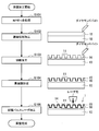
- FIG. 6 is a diagram schematically showing a cross section when the master 1 in each step is cut in the thickness direction, along with the flow of the method for manufacturing the master 1 according to the present embodiment.
- step S101 the surface layer 16 is formed on the surface of the substrate 10 using a method such as plating such as electrolytic plating or electroless plating. Note that step S101 for forming the surface layer 16 may be omitted.
- step S102 the surface of the surface layer 16 is subjected to mirror cutting using a diamond cutting tool or the like with an ultra-precision cutting machine to flatten the surface of the surface layer 16 or the surface of the substrate 10.
- the process is not limited to mirror cutting using a diamond cutting tool, and mirror polishing using fixed abrasive grains and polishing using free abrasive grains may be used.
- step S103 the main concavo-convex portion 11 extending in the surface direction of the base material 10 is formed on the surface of the surface layer 16 or the surface of the base material 10 using a diamond cutting tool or the like with an ultraprecision cutting machine. Note that this step is not limited to ultra-precise cutting using a diamond tool, and photolithography or laser processing may be used. Moreover, you may use as the base material 10 what was transferred by electroforming from the type
- step S104 a method such as electroplating or electroless plating, sputtering, vapor deposition, ion plating, CVD (Chemical Vapor Deposition), spin coating, coating, slit coating, dip coating, or spray coating is used. Then, the covering layer 15 covering the surface of the main concavo-convex portion 11 is formed. Note that step S104 for forming the coating layer 15 may be omitted.
- step S105 the surface of the main uneven portion 11 is irradiated with an ultrashort pulse laser having a pulse width of 10 picoseconds or less on the surface of the main uneven portion 11 using the laser processing apparatus 8.
- the master 1 is manufactured by forming the fine concavo-convex portions 14 having a narrow pitch compared to the above. Details of the laser processing apparatus 8 will be described later.
- the shape and the like of the fine irregularities 14 change depending on the laser irradiation conditions such as laser wavelength, repetition frequency, pulse width, fluence, number of pulses, beam size, scanning speed, scanning direction, beam scanning pitch, and polarization direction. The irradiation conditions are selected so that the fine irregularities 14 are obtained.
- the fluence per shot of the ultrashort pulse laser when the master 1 is manufactured is larger than 0.16 J / cm 2 .
- the irradiated laser light causes interference and diffraction, and the laser intensity on the surface of the main concavo-convex portion 11 periodically changes according to the position. Due to the periodic change of the laser intensity, the fine uneven portions 14 having different widths and depths according to the positions can be formed on the surface of the main uneven portion 11.
- the periodic change in the laser intensity can be obtained by calculation based on the shape of the main uneven portion 11 and the wavelength of the laser.
- the desired fine irregularities 14 can be formed on the master 1. Furthermore, by producing the transfer 5 using the master 1 having the desired fine irregularities 14, the fine irregularities 54 optimized according to the properties of the fluid used in the transfer 5 are formed on the transfer 5. It can be formed on the surface.
- FIG. 7 is a diagram showing the spot width of the ultrashort pulse laser and the irradiation method in the manufacturing process of the master 1.
- FIG. 7A shows a case where the laser spot width is reduced and the laser is irradiated only on the bottom surface of the concave portion 13 of the master 1. In this case, the fine uneven portion 14 is formed only on the bottom surface of the concave portion 13 of the master 1.
- FIG. 7B shows a case where the laser spot width is reduced as in FIG. 7A and the laser is irradiated only on the upper surface of the convex portion 12.
- the fine uneven part 14 is formed only on the upper surface of the convex part 12. Further, as shown in FIG. 7C, the entire surface of the main concavo-convex portion 11 may be irradiated with laser without reducing the laser spot width. In this case, fine irregularities 14 are formed on both the bottom surface of the recess 13 and the upper surface of the projection 12.
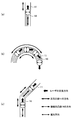
- FIG. 8 is a diagram showing an example of the irradiation direction of the ultrashort pulse laser in the manufacturing process of the master 1.
- the polarization direction of the laser light is also shown.
- FIG. 8A shows an example of the laser scanning direction when scanning is performed along the main concavo-convex portion 11 extending in the surface direction of the substrate 10.
- FIG. 8B shows an example of the laser scanning direction when scanning is performed along the main concavo-convex portion 11 having a planar shape curved in a curved shape on the surface of the substrate 10.
- 8C shows an example of the laser scanning direction when scanning is performed along the main concavo-convex portion 11 having a planar shape bent so as to form an obtuse angle on the surface of the substrate 10.
- the laser beam is linearly polarized light
- the polarization direction is orthogonal to the longitudinal direction of the main concavo-convex portion 11.
- the laser beam may be linearly polarized, elliptically polarized, or circularly polarized. Furthermore, by changing the polarization direction and the scanning direction, the formation direction, shape, and the like of the fine uneven portion 14 can be changed.
- FIG. 9 is a diagram showing the polarization direction and scanning direction of the ultrashort pulse laser and the planar shape of the fine uneven portion 14 in the manufacturing process of the master 1.
- FIG. 9A shows an example of linearly polarized light, in which the polarization direction is orthogonal to the longitudinal direction of the main concavo-convex portion 11 and the laser is scanned along the longitudinal direction of the main concavo-convex portion 11.
- each fine uneven portion 14 extending along the longitudinal direction of the main uneven portion 11 is formed.
- FIG. 9B shows an example of linearly polarized light, in which the polarization direction is the same as the longitudinal direction of the main concavo-convex portion 11 and the laser is scanned along the longitudinal direction of the main concavo-convex portion 11.
- the fine uneven part 14 extending in the direction orthogonal to the longitudinal direction of the main uneven part 11 is formed.
- FIG. 9C shows an example of linearly polarized light, in which the polarization direction is inclined with respect to the longitudinal direction of the main concavo-convex portion 11 and the laser is scanned along the longitudinal direction of the main concavo-convex portion 11.
- the fine concavo-convex portion 14 having a direction perpendicular to the polarization direction and inclined with respect to the longitudinal direction of the main concavo-convex portion 11 is formed.
- FIG. 9D shows a case where the laser is scanned along the longitudinal direction of the main concavo-convex portion 11 using circularly polarized light. In this case, dot-like or mesh-like fine irregularities 14 having no anisotropy are formed.
- FIG. 9C shows an example of linearly polarized light, in which the polarization direction is inclined with respect to the longitudinal direction of the main concavo-convex portion 11 and the laser is scanned along the longitudinal direction of the main concavo-convex portion 11.
- 9E shows a case where the laser is scanned along the longitudinal direction of the main concavo-convex portion 11 while changing the polarization direction for each position.
- the fine concavo-convex portion 14 having a different shape for each position is formed.
- the desired fine uneven portion 14 can be formed by changing the laser spot width, scanning direction, polarization direction, and the like. Since the laser spot width, scanning direction, polarization direction, and the like can be freely controlled, the desired fine uneven portion 14 can be easily formed.
- FIG. 10 is a schematic view showing an example of the configuration of a laser processing apparatus 8 for producing the plate-shaped master 1.
- the laser body 340 is, for example, IFRIT (trade name) manufactured by Cyber Laser Corporation.
- the wavelength of the laser used for laser processing is, for example, 800 nm. However, the wavelength of the laser used for laser processing may be 400 nm or 266 nm.
- the repetition frequency is preferably larger in consideration of the processing time and the narrow pitch of the concave portion 13 or the convex portion 12 to be formed, and is preferably 1,000 Hz or more.
- the pulse width of the laser is preferably short, and is preferably about 200 femtoseconds (10 ⁇ 15 seconds) to 10 picoseconds (10 ⁇ 12 seconds).
- the laser body 340 emits laser light linearly polarized in the vertical direction. Therefore, in the laser processing apparatus 8 according to the present embodiment, linear polarization or circular polarization in a desired direction is obtained by rotating the polarization direction using a wave plate 341 (for example, a ⁇ / 2 wave plate). I have to.
- the intensity distribution of the laser light is a Gaussian distribution.
- the laser beam is focused using two orthogonal cylindrical lenses 343 so that a desired beam size is obtained. Note that the laser light may be narrowed by a spherical lens.
- the linear stage 344 When processing the plate-shaped master 1, the linear stage 344 is moved at a constant speed. Further, when it is desired to perform processing on a surface larger than the size of the beam spot, an uneven shape is imparted to the entire surface to be processed by scanning the beam.
- the fluence in the present embodiment is an energy density peak value per shot (one pulse). That is, a beam profile is measured using a beam profiler (SP620U manufactured by Offiel, and software BeamStar), Gaussian fitting is applied to the cross-sectional profile, and the peak value of the power density (W / cm 2 ) The value obtained by converting the energy density per pulse (J / cm 2 ) by dividing by the repetition frequency (Hz) was used as the fluence.
- the fluence in the case of a top hat type beam can be obtained by applying a top hat type fitting and similarly obtaining the energy density from the top value of the power density.
- Desired fine irregularities 14 can be formed on the coating layer 15.
- the transfer product 5 is manufactured by the imprint transfer method using the master 1 according to the present embodiment. As described above, by using the imprint transfer method, it is possible to easily mass-produce the transfer product 5 having a highly hydrophilic region. With reference to FIG. 11, the manufacturing method of the transcription
- FIG. 11 is a diagram schematically showing a cross section when the transfer product 5 in each step is cut in the thickness direction, along with a flow of a method of manufacturing the transfer product 5 using the master 1 according to the present embodiment.
- step S201 the master 1 is cleaned. Furthermore, a mold release process for preventing adhesion of the curable hydrophilic resin 56 is performed on the surface of the main uneven portion 11 of the master 1.
- step S202 the curable hydrophilic resin 56 is applied to the surface of the master 1 on which the main concavo-convex portion 11 is provided by using a coating apparatus to form the resin layer 55.
- the coating apparatus includes coating means such as a gravure coater, a wire bar coater, or a die coater.
- the base material 50 is pressed against the resin layer 55 in step S203.
- the main uneven portion 11 of the master 1 is filled with a curable hydrophilic resin 56 that is a composition of the resin layer 55.
- the fine uneven portion 14 provided on the surface of the main uneven portion 11 is also filled with the curable hydrophilic resin 56.
- the curable hydrophilic resin 56 is cured. If the curable hydrophilic resin 56 is a thermosetting type, heat is applied to the resin layer 55. If the curable hydrophilic resin 56 is a photocurable type, the resin layer 55 is irradiated with light, and the curable hydrophilic resin 56 is irradiated. Is cured. In the following description, the curable hydrophilic resin 56 is described as being an ultraviolet curable hydrophilic resin.
- the ultraviolet curable hydrophilic resin is a resin that cures when irradiated with light having a wavelength in the ultraviolet region.
- the resin layer 55 is irradiated with ultraviolet rays to cure the ultraviolet curable hydrophilic resin 56. Irradiation with ultraviolet rays can be performed by using, for example, an ultraviolet lamp.
- step S204 after the ultraviolet curable hydrophilic resin 56 that is the composition of the resin layer 55 is cured, the resin layer 55 is released from the master 1. At this time, if the resin layer 55 is attached to the base material 50, the resin layer 55 is released from the master 1 together with the base material 50. In this manner, the transfer product 5 having the resin layer 55 to which the shape of the main uneven portion 11 of the master 1 is transferred can be manufactured.
- the main concavo-convex portion 51 formed on the resin layer 55 of the transferred product 5 has a shape to which the main concavo-convex portion 11 of the master 1 is transferred. Further, a fine uneven portion 54 is formed on the surface of the main uneven portion 51, and the fine uneven portion 54 has a shape to which the fine uneven portion 14 of the master 1 is transferred.
- a further transferred product 5 may be produced by further transferring using the transferred product 5 manufactured as described above as a replica master.
- the transfer product 5 can be easily mass-produced by performing imprint transfer using the master 1. Moreover, since the fine unevenness
- transfer 5 can be improved.
- cylindrical master 1 it is possible to perform imprinting by a roll-to-roll method, which can further increase mass productivity.
- the transfer product 5 by performing imprint transfer using the master 1, the transfer product 5 can be easily mass-produced. Further, since the fine uneven portion 54 can be provided on the surface of the main uneven portion 51 of the transferred material 5, the transfer material 5 having the hydrophilicity of the surface of the main uneven portion 51 can be easily mass-produced. Is possible.
- the shape and the like of the fine irregularities 14 formed on the master 1 can be easily changed by changing the laser irradiation conditions used when manufacturing the master 1. Therefore, according to the present embodiment, the desired fine uneven portion 14 can be formed on the master 1, and the desired fine uneven portion 54 can also be formed on the transfer 5 by transferring using the master 1. Can do. Further, since it is possible to change the shape of the fine uneven portion 54 of the transfer product 5, the flowability (flow velocity) of the fluid flowing through the main uneven portion 51 can be controlled by changing the shape of the fine uneven portion 54. You can also.
- the master 1 and the transcript 5 according to the embodiment of the present invention will be specifically described with reference to Examples and Comparative Examples.
- the Example shown below is an example of the master 1 and the transcription
- the master 1 according to Examples 1 to 6 and the comparative example was manufactured by the following method.
- Example 1 The surface of the base material 10 of SUS420 (martensitic stainless steel) 10 mm thick and 25 mm square was subjected to NiP plating treatment having a thickness of 150 ⁇ m to form a surface layer 16 made of NiP.
- a plurality of concave portions 13 extending linearly in the plane of the base material 10 are formed by a diamond tool using an ultraprecision cutting machine.
- a plurality of main irregularities 11 were formed. Specifically, the width of the bottom surface of the concave portion 13 was 40 ⁇ m, the depth of the concave portion 13 from the surface of the base material 10 was 120 ⁇ m, and the pitch (period) of the main concave and convex portions 11 was 200 ⁇ m.
- DLC coating was performed on the surface of the main concavo-convex portion 11 to form a coating layer 15 made of DLC having a thickness of 1 ⁇ m.
- the surface of the main concavo-convex portion 11 was irradiated with an ultrashort pulse laser.
- Laser irradiation was performed using an ultrashort pulse laser processing apparatus 8 having a wavelength of 780 nm, a pulse width of 200 fs, a repetition frequency of 1 kHz, a maximum output of 1 W, and linearly polarized light.
- a beam was shaped through a lens to obtain a Gaussian beam having a size of about ⁇ 400 ⁇ m on the surface of the main uneven portion 11.
- the fluence per shot of the ultrashort pulse laser was 0.31 J / cm 2, and the angle of the wave plate on the optical path was set so that the polarization direction of the laser was orthogonal to the longitudinal direction of the main concavo-convex portion 11. Furthermore, the laser was irradiated to the whole surface of the main concavo-convex portion 11 by causing the laser to scan in the longitudinal direction of the main concavo-convex portion 11 at a scanning speed of 20 mm / s while overlapping at a pitch of 80 ⁇ m.
- the master 1 according to Example 1 was manufactured through the above steps.
- Example 2 A master was prepared in the same manner as in Example 1 except that the laser irradiation fluence was 0.28 J / cm 2 .
- Example 3 A master was produced in the same manner as in Example 1 except that the laser irradiation fluence was changed to 0.25 J / cm 2 .
- Example 4 A master was produced in the same manner as in Example 1 except that the laser irradiation fluence was 0.22 J / cm 2 .
- Example 5 A master was produced in the same manner as in Example 1 except that the laser irradiation fluence was 0.19 J / cm 2 .
- the substrate 10 is made of SUS304 (stainless steel), and the surface has a wavelength of 515 nm, a pulse width of 3 ps, a repetition frequency of 50 kHz, a maximum output of 7.7 W, a beam size of about 100 ⁇ m ⁇ 100 ⁇ m (top hat beam profile), and a scanning pitch of 100 ⁇ m.
- the master 1 was prepared by processing under conditions of a scanning speed of 31 mm / s and a laser irradiation fluence of 0.08 J / cm 2 .
- Example 2 A master was produced in the same manner as in Example 1 except that the ultrashort pulse laser irradiation was not performed.
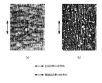
- FIG. 12 is an SEM image of the surface of the main concavo-convex portion 11 of the master 1 according to Example 4 observed.
- FIG. 12A is an SEM image obtained by observing the upper surface of the convex portion 12 of the master 1
- FIG. 12B is an SEM image obtained by observing the bottom surface of the concave portion 13 of the master 1.
- the fine irregularities 14 are formed on the top surface of the convex portion 12 and the bottom surface of the concave portion 13. Further, the fine uneven portion 14 is formed so as to extend along the longitudinal direction of the main uneven portion 11.
- the fineness formed on the upper surface of the convex portion 12 is changed.
- a difference occurs in the width of the fine uneven portion 14 and the depth of the fine recessed portion 18 between the uneven portion 14 and the fine uneven portion 14 formed on the bottom surface of the recessed portion 13. Further, even within the bottom surface of the concave portion 13, the width of the fine concave and convex portion 14 and the depth of the fine concave portion 18 have different values for each position.
- a transfer product 5 was prepared by the steps described below.
- an ultraviolet curable hydrophilic resin 56 made of an acrylic resin acrylate is applied to the surface of the master 1 on which the main concavo-convex portion 11 is provided to form a resin layer 55.
- the resin base material 50 is pressed against the resin layer 55.
- the ultraviolet ray curable hydrophilic resin 56 is cured by irradiating the resin layer 55 with ultraviolet rays having a central wavelength of 365 nm using an ultraviolet lamp. Further, the resin layer 55 was released from the master 1 to produce the transfer products 5 according to Examples 1 to 6 and the comparative example.
- FIGS. 13A to 13E are AFM data of the fine concavo-convex portion 54 formed on the bottom surface of the concave portion 53 of the transfer product 5 formed using the master 1 according to the first to fifth embodiments. Furthermore, based on these AFM data, the arithmetic average roughness (Ra) and specific surface area ratio of the bottom surface of the concave portion 53 of each transferred product 5 were calculated.
- the pure water contact angle on the bottom surface of the concave portion 53 of the transfer product 5 according to Examples 1 to 6 and the comparative example was measured.
- the pure water contact angle can be used as a hydrophilic index, and the smaller the value, the higher the hydrophilicity.
- the pure contact angle is measured using an automatic contact angle meter CA-V (manufactured by Kyowa Interface Science Co., Ltd.), pure water is put into a syringe, and a stainless steel needle is attached to the tip of the syringe. Then, 1 ⁇ L of the dropping amount is dropped on the bottom surface of the recess 53 to perform measurement.
- the arithmetic average roughness, the specific surface area ratio, and the pure contact angle of the bottom surface of the concave portion 53 of the transcript 5 according to Examples 1 to 6 and the comparative example are the processing conditions (the value of the laser irradiation fluence) when the master 1 is manufactured. Along with the material of the laser irradiation part of the master 1, it is shown in Table 1 below.
- a fine uneven structure that is, a fine uneven portion 54 is formed on the bottom surface of the recessed portion 53 of the transcript 5 according to Examples 1 to 5. This is because the shape of the fine uneven portion 14 formed on the surface of the convex portion 12 of the master 1 is transferred to the transfer product 5.
- the liquid flow rate was faster and the hydrophilicity was improved as compared with the comparative example. Furthermore, it can be seen that the hydrophilicity of the bottom surface of the concave portion 53 of the transfer product 5 according to Examples 1 to 6 is improved because the contact angle of pure water is smaller than that of the comparative example. This is considered to be because the fine uneven portion 54 is provided on the bottom surface of the concave portion 53 of the transfer product 5.
- a fine uneven portion 54 is formed on the bottom surface of the concave portion 53 of the transfer product 5, and the bottom surface of the concave portion 53 of the transfer product 5 has an arithmetic average roughness of 10 nm to 150 nm and a ratio of 1.1 to 3.0. It was found that when the surface area ratio is high, the hydrophilicity is improved as compared with the transfer product 5 without the fine unevenness portion 54 according to the comparative example.
- the material of the laser irradiation part of Example 6 is SUS304 (stainless steel)
- the laser irradiation of the master 1 of Examples 1 to 5 is performed. It was found that the fine irregularities 54 of the transferred product 5 having the arithmetic average roughness Ra and the specific surface area ratio equivalent to the case where the material of the portion is DLC are formed, and the hydrophilicity is improved. This shows that the suitable fluence range varies depending on the material of the laser irradiation part.
- the same result as SUS304 is obtained also when the material is Cu or Ni.
Landscapes
- Chemical & Material Sciences (AREA)
- Engineering & Computer Science (AREA)
- Health & Medical Sciences (AREA)
- Mechanical Engineering (AREA)
- Chemical Kinetics & Catalysis (AREA)
- Manufacturing & Machinery (AREA)
- Analytical Chemistry (AREA)
- General Health & Medical Sciences (AREA)
- Dispersion Chemistry (AREA)
- Hematology (AREA)
- Clinical Laboratory Science (AREA)
- Physics & Mathematics (AREA)
- Microelectronics & Electronic Packaging (AREA)
- General Physics & Mathematics (AREA)
- Organic Chemistry (AREA)
- Thermal Sciences (AREA)
- Electromagnetism (AREA)
- Toxicology (AREA)
- Oral & Maxillofacial Surgery (AREA)
- Computer Hardware Design (AREA)
- Life Sciences & Earth Sciences (AREA)
- Biochemistry (AREA)
- Immunology (AREA)
- Pathology (AREA)
- Shaping Of Tube Ends By Bending Or Straightening (AREA)
- Moulds For Moulding Plastics Or The Like (AREA)
- Physical Or Chemical Processes And Apparatus (AREA)
- Micromachines (AREA)
Abstract
Description
原盤1は、マイクロ流路を作製するための原盤であり、ロールツーロール(roll-to-roll)方式等も含むインプリント転写に用いられる。すなわち、原盤1の表面に設けられた凹凸形状を転写することで、転写物5を製造する。なお、原盤1を用いてインプリント転写により転写物5を得た場合には、転写物5の表面には、原盤1の表面に設けられた凹凸形状を反転させた形状の凹凸が形成されることとなる。転写物5の表面に形成された凹部がマイクロ流路となる。
以下に、本実施形態に係る原盤1を用いてインプリント転写を行って製造した転写物5を説明する。まず、図5を参照して、本発明の一実施形態に係る転写物5について説明する。図5は、本実施形態に係る転写物5を厚み方向に切断した際の断面を模式的に示した図である。
本実施形態に係る転写物5を含む、マイクロリアクター等といったマイクロ流体チップを作製することができる。例えば、上記の転写物5を含むマイクロ流体チップにおいては、転写物5の凹部53が、流体を流すためのマイクロ流路となることができ、もしくは、流体を溜めるためのウェルとなることができる。この場合には、転写物5の凹部53の底面に微細凹凸部54が設けられることにより、凹部53の底面の表面積がより大きくなり、凹部53の底面の親水性を高めることができる。また、凹部53の底面の微細凹凸部54に流体が流れこむと、流体と微細凹凸部54との界面での作用により、流体の流動性が変化する。したがって、微細凹凸部54の形状を変えることにより、凹部53に流れる流体の流れやすさを制御することができる。したがって、凹部53に流れる流体の性質に応じて微細凹凸部54の形状を選択することが可能である。
図6を参照して、本実施形態に係る原盤1の製造方法について説明する。図6は、本実施形態に係る原盤1の製造方法のフローとともに、各工程における原盤1を厚み方向に切断した際の断面を模式的に示した図を示す。
さらに、図10を参照して、本実施形態に係る原盤1の製造方法にて使用されるレーザ加工装置8の構成例について説明する。
本実施形態においては、本実施形態に係る原盤1を用いて、インプリント転写法により転写物5を製造する。このように、インプリント転写法を用いることにより、親水性の高い領域を有する転写物5を容易に大量生産することができる。図11を参照して、本実施形態に係る転写物5の製造方法について説明する。図11は、本実施形態に係る原盤1を用いた転写物5の製造方法のフローとともに、各工程における転写物5を厚み方向に切断した際の断面を模式的に示した図を示す。
以下の方法により、実施例1~6及び比較例に係る原盤1を製造した。
10mm厚、25mm四方のSUS420(マルテンサイト系ステンレス鋼)の基材10の表面に、厚さ150μmのNiPメッキ処理を施し、NiPからなる表面層16を形成した。
レーザの照射フルエンスを0.28J/cm2とした以外は、実施例1と同様に原盤を作製した。
レーザの照射フルエンスを0.25J/cm2とした以外は、実施例1と同様に原盤を作製した。
レーザの照射フルエンスを0.22J/cm2とした以外は、実施例1と同様に原盤を作製した。
レーザの照射フルエンスを0.19J/cm2とした以外は、実施例1と同様に原盤を作製した。
基材10をSUS304(ステンレス鋼)とし、その表面に、波長515nm、パルス幅3ps、繰り返し周波数50kHz、最大出力7.7W、ビームサイズ約100μm×100μm(トップハット型のビームプロファイル)、走査ピッチ100μm、走査速度31mm/s、レーザの照射フルエンス0.08J/cm2の条件で加工し、原盤1を作成した。
超短パルスレーザ照射を行わなかった点以外は、実施例1と同様に原盤を作製した。
上記の工程により製造した原盤1の評価を行った。具体的には、上記の工程により製造した実施例4に係る原盤1の微細凹凸部14を走査型電子顕微鏡(Scanning Electron Microscope:SEM)を用いて観察した。図12を用いて、実施例4に係る原盤1のSEMの観察結果を説明する。図12は、実施例4に係る原盤1の主凹凸部11の表面を観察したSEM画像である。詳細には、図12(a)は、原盤1の凸部12の上面を観察したSEM画像であり、図12(b)は、原盤1の凹部13の底面を観察したSEM画像である。これらのSEM画像からわかるように、微細凹凸部14は、凸部12の上面及び凹部13の底面に形成されている。さらに、微細凹凸部14は、主凹凸部11の長手方向に沿って延びるように形成されている。
上記の工程により製造した実施例1~6及び比較例に係る原盤1を用いて、下記に説明する工程により転写物5を作製した。
実施例1~6に係る原盤1を用いて形成した転写物5の凹部53の底面に形成された微細凹凸部54をAFMにより観察した。図13を用いて、実施例1~5に係る転写物5の微細凹凸部54のAFMの観察結果を説明する。図13(a)~(e)は、実施例1~5に係る原盤1を用いて形成された転写物5の凹部53の底面に形成された微細凹凸部54のAFMデータである。さらに、これらのAFMデータに基づいて、各転写物5の凹部53の底面の算術平均粗さ(Ra)及び比表面積率を算出した。

5 転写物
8 レーザ加工装置
10、50 基材
11、51 主凹凸部
12、52 凸部
13、53 凹部
14、54 微細凹凸部
17、57 微細凸部
18、58 微細凹部
15 被覆層
16 表面層
340 レーザ本体
341 波長板(例えば、λ/2波長板)
343 シリンドリカルレンズ
344 リニアステージ
55 樹脂層
56 硬化型親水性樹脂
Claims (13)
- 基材と、
前記基材の表面に設けられ、前記基材の面方向に延びる主凹凸部と、
前記主凹凸部の表面に設けられ、前記主凹凸部と比べてピッチが狭い微細凹凸部と、
を備え、
前記微細凹凸部は、10nm~150nmの算術平均粗さを有し、且つ、1.1~3.0の比表面積率を有する、マイクロ流路作製用原盤。 - 前記主凹凸部は、1μm~2000μmの幅及び深さを有し、
前記微細凹凸部は、30nm~1000nmの幅及び深さを有する、
請求項1に記載のマイクロ流路作製用原盤。 - 複数の前記微細凹凸部を備え、
前記微細凹凸部の幅及び深さは、前記微細凹凸部が形成される位置ごとに異なる値となる、請求項2に記載のマイクロ流路作製用原盤。 - 前記微細凹凸部は、前記主凹凸部の長手方向に沿って延びるように設けられている、請求項1から3のいずれか1項に記載のマイクロ流路作製用原盤。
- 基材の表面に、前記基材の面方向に延びる主凹凸部を形成し、
前記主凹凸部の表面に10ピコ秒以下のパルス幅を有する超短パルスレーザを照射することで、前記主凹凸部の表面に、前記主凹凸部と比べてピッチが狭い微細凹凸部を形成する、
ことを含むマイクロ流路作製用原盤の製造方法。 - 前記超短パルスレーザの照射は、偏光方向が前記主凹凸部の長手方向と直交するようにして行われる、請求項5に記載のマイクロ流路作製用原盤の製造方法。
- 請求項1から4のいずれか1項に記載のマイクロ流路作製用原盤の表面形状が転写された樹脂層を含む転写物。
- 樹脂層と、
前記樹脂層の表面に設けられ、前記樹脂層の面方向に延びる主凹凸部と、
前記主凹凸部の表面に設けられ、前記主凹凸部と比べてピッチが狭い微細凹凸部と、
を備え、
前記微細凹凸部は、10nm~150nmの算術平均粗さを有し、且つ、1.1~3.0の比表面積率を有する、転写物。 - 前記主凹凸部は、1μm~2000μmの幅及び深さを有し、
前記微細凹凸部は、30nm~1000nmの幅及び深さを有する、
請求項8に記載の転写物。 - 複数の前記微細凹凸部を備え、
前記微細凹凸部の幅及び深さは、前記微細凹凸部が形成される位置ごとに異なる値となる、
請求項9に記載の転写物。 - 前記微細凹凸部は、前記主凹凸部の長手方向に沿って延びるように設けられている、請求項8から10のいずれか1項に記載の転写物。
- 前記樹脂層は硬化型親水性樹脂からなる、請求項7から11のいずれか1項に記載の転写物。
- 請求項8から12のいずれか1項に記載の転写物を含むマイクロ流体チップ。
Priority Applications (3)
| Application Number | Priority Date | Filing Date | Title |
|---|---|---|---|
| US15/531,267 US10850273B2 (en) | 2014-11-28 | 2015-10-26 | Master for micro flow path creation, transfer copy, and method for producing master for micro flow path creation |
| GB1708703.2A GB2550694B (en) | 2014-11-28 | 2015-10-26 | Master for micro flow path creation, transfer copy, and method for producing master for micro flow path creation |
| US16/927,425 US12194459B2 (en) | 2014-11-28 | 2020-07-13 | Master for micro flow path creation, transfer copy, and method for producing master for micro flow path creation |
Applications Claiming Priority (2)
| Application Number | Priority Date | Filing Date | Title |
|---|---|---|---|
| JP2014-241728 | 2014-11-28 | ||
| JP2014241728A JP6796371B2 (ja) | 2014-11-28 | 2014-11-28 | マイクロ流路作製用原盤の製造方法 |
Related Child Applications (2)
| Application Number | Title | Priority Date | Filing Date |
|---|---|---|---|
| US15/531,267 A-371-Of-International US10850273B2 (en) | 2014-11-28 | 2015-10-26 | Master for micro flow path creation, transfer copy, and method for producing master for micro flow path creation |
| US16/927,425 Continuation US12194459B2 (en) | 2014-11-28 | 2020-07-13 | Master for micro flow path creation, transfer copy, and method for producing master for micro flow path creation |
Publications (1)
| Publication Number | Publication Date |
|---|---|
| WO2016084533A1 true WO2016084533A1 (ja) | 2016-06-02 |
Family
ID=56074109
Family Applications (1)
| Application Number | Title | Priority Date | Filing Date |
|---|---|---|---|
| PCT/JP2015/080104 Ceased WO2016084533A1 (ja) | 2014-11-28 | 2015-10-26 | マイクロ流路作製用原盤、転写物、およびマイクロ流路作製用原盤の製造方法 |
Country Status (4)
| Country | Link |
|---|---|
| US (2) | US10850273B2 (ja) |
| JP (1) | JP6796371B2 (ja) |
| GB (1) | GB2550694B (ja) |
| WO (1) | WO2016084533A1 (ja) |
Cited By (3)
| Publication number | Priority date | Publication date | Assignee | Title |
|---|---|---|---|---|
| CN109759151A (zh) * | 2019-01-30 | 2019-05-17 | 浙江工业大学 | 一种基于条状的梯度阵列与楔形流道构成的自驱动纸基微流控芯片 |
| WO2022205529A1 (zh) * | 2021-03-31 | 2022-10-06 | 苏州大学 | 多层微流控芯片封装器件、多层微流控芯片及其应用 |
| EP3971568A4 (en) * | 2019-05-15 | 2022-11-30 | Denka Company Limited | BACKING FILM AND INSPECTION KIT |
Families Citing this family (7)
| Publication number | Priority date | Publication date | Assignee | Title |
|---|---|---|---|---|
| JP6796371B2 (ja) * | 2014-11-28 | 2020-12-09 | デクセリアルズ株式会社 | マイクロ流路作製用原盤の製造方法 |
| US9844906B2 (en) * | 2015-12-10 | 2017-12-19 | S.D. Warren Company | Release webs and textured products |
| WO2020085288A1 (ja) * | 2018-10-22 | 2020-04-30 | デクセリアルズ株式会社 | 原盤、原盤の製造方法及び転写物の製造方法 |
| CN114096855A (zh) * | 2019-07-08 | 2022-02-25 | 积水化学工业株式会社 | 送液方法以及检测芯片 |
| EP4106969A1 (en) * | 2020-02-17 | 2022-12-28 | Hella Gmbh & Co. Kgaa | Method of manufacturing a mould for injection moulding |
| KR102872664B1 (ko) * | 2021-12-23 | 2025-10-17 | 한국과학기술원 | 마이크로 웰 성형 장치 및 마이크로 웰을 가지는 디스크 제조 방법 |
| WO2023121114A1 (ko) * | 2021-12-23 | 2023-06-29 | 한국과학기술원 | 마이크로 웰 성형 장치 및 마이크로 웰을 가지는 디스크 제조 방법 |
Citations (5)
| Publication number | Priority date | Publication date | Assignee | Title |
|---|---|---|---|---|
| WO2005123242A1 (ja) * | 2004-06-15 | 2005-12-29 | Nec Corporation | 構造体ならびにこれを用いたチップ、および親/疎液性の制御方法 |
| JP2006103107A (ja) * | 2004-10-04 | 2006-04-20 | Mitsui Chemicals Inc | 平版印刷用原版 |
| JP2008062561A (ja) * | 2006-09-08 | 2008-03-21 | Stanley Electric Co Ltd | 親水性積層膜を備えた物品の製造方法、および、親水性積層膜を備えた物品 |
| JP2012037389A (ja) * | 2010-08-06 | 2012-02-23 | Fujikura Ltd | マイクロ流体チップの製造方法、マイクロ流体チップ、及び表面プラズモン共鳴光の発生装置 |
| JP2014136304A (ja) * | 2013-01-18 | 2014-07-28 | Dainippon Printing Co Ltd | 成形型及びその製造方法、並びに構造物及びその製造方法 |
Family Cites Families (23)
| Publication number | Priority date | Publication date | Assignee | Title |
|---|---|---|---|---|
| US6451264B1 (en) * | 2000-01-28 | 2002-09-17 | Roche Diagnostics Corporation | Fluid flow control in curved capillary channels |
| JP2003001830A (ja) * | 2001-06-22 | 2003-01-08 | Canon Inc | インクジェット記録ヘッドのインク吐出口製造方法、および該製造方法によって製造されたインク吐出口を有するインクジェット記録ヘッド |
| JP4263865B2 (ja) | 2002-01-22 | 2009-05-13 | 独立行政法人科学技術振興機構 | 超短パルスレーザーを用いた微細加工方法及びその加工物 |
| US7105809B2 (en) * | 2002-11-18 | 2006-09-12 | 3M Innovative Properties Company | Microstructured polymeric substrate |
| DE10326607A1 (de) | 2003-06-13 | 2005-01-05 | Steag Microparts Gmbh | Vorrichtung zum Handhaben von Flüssigkeiten |
| JP4292405B2 (ja) | 2004-02-16 | 2009-07-08 | Jsr株式会社 | 検査素子用のチップ基板およびその製造方法 |
| JP4513626B2 (ja) | 2005-03-28 | 2010-07-28 | 住友ベークライト株式会社 | マイクロチャネル基板作製用鋳型の作製方法 |
| JP4900245B2 (ja) | 2005-11-14 | 2012-03-21 | 日本電気株式会社 | マイクロチップおよびその使用方法、ならびに質量分析システム |
| JP2008126283A (ja) * | 2006-11-21 | 2008-06-05 | Seiko Epson Corp | 微細構造体の製造方法、露光方法 |
| JP2008194573A (ja) * | 2007-02-09 | 2008-08-28 | Matsushita Electric Ind Co Ltd | 脂質二重膜形成方法 |
| JPWO2009145022A1 (ja) | 2008-05-27 | 2011-10-06 | コニカミノルタエムジー株式会社 | 微細流路を備えたマイクロチップ |
| JP2009295797A (ja) * | 2008-06-05 | 2009-12-17 | Kyowa Hakko Chemical Co Ltd | 溝構造または中空構造を有する部材の作製方法 |
| JP2010236955A (ja) | 2009-03-30 | 2010-10-21 | Fujifilm Corp | マイクロ流路 |
| WO2010113545A1 (ja) | 2009-03-31 | 2010-10-07 | コニカミノルタオプト株式会社 | 射出成形用マスター型の製造方法、射出成形用マスター型及び射出成形用金型 |
| JP5344400B2 (ja) * | 2009-11-11 | 2013-11-20 | 国立大学法人大阪大学 | モルフォ型構造色発色体の製造方法 |
| JP2011169695A (ja) | 2010-02-17 | 2011-09-01 | Sharp Corp | 送液装置 |
| KR101348655B1 (ko) | 2010-03-24 | 2014-01-08 | 한국전자통신연구원 | 미세유체 제어 장치 및 그 제조 방법 |
| JP5866765B2 (ja) * | 2010-04-28 | 2016-02-17 | ソニー株式会社 | 導電性素子およびその製造方法、配線素子、情報入力装置、表示装置、ならびに電子機器 |
| JP5420584B2 (ja) * | 2011-04-21 | 2014-02-19 | キヤノンマシナリー株式会社 | 二酸化チタン光触媒層のパターン形成方法 |
| US9981844B2 (en) | 2012-03-08 | 2018-05-29 | Infineon Technologies Ag | Method of manufacturing semiconductor device with glass pieces |
| JP2014109564A (ja) | 2012-12-04 | 2014-06-12 | National Institute Of Advanced Industrial & Technology | 標的物質検出用マイクロチップ |
| JP5977190B2 (ja) | 2013-03-29 | 2016-08-24 | 住友理工株式会社 | 表面改質部材およびその製造方法、並びにマイクロ流路装置およびその製造方法 |
| JP6796371B2 (ja) * | 2014-11-28 | 2020-12-09 | デクセリアルズ株式会社 | マイクロ流路作製用原盤の製造方法 |
-
2014
- 2014-11-28 JP JP2014241728A patent/JP6796371B2/ja active Active
-
2015
- 2015-10-26 US US15/531,267 patent/US10850273B2/en active Active
- 2015-10-26 WO PCT/JP2015/080104 patent/WO2016084533A1/ja not_active Ceased
- 2015-10-26 GB GB1708703.2A patent/GB2550694B/en active Active
-
2020
- 2020-07-13 US US16/927,425 patent/US12194459B2/en active Active
Patent Citations (5)
| Publication number | Priority date | Publication date | Assignee | Title |
|---|---|---|---|---|
| WO2005123242A1 (ja) * | 2004-06-15 | 2005-12-29 | Nec Corporation | 構造体ならびにこれを用いたチップ、および親/疎液性の制御方法 |
| JP2006103107A (ja) * | 2004-10-04 | 2006-04-20 | Mitsui Chemicals Inc | 平版印刷用原版 |
| JP2008062561A (ja) * | 2006-09-08 | 2008-03-21 | Stanley Electric Co Ltd | 親水性積層膜を備えた物品の製造方法、および、親水性積層膜を備えた物品 |
| JP2012037389A (ja) * | 2010-08-06 | 2012-02-23 | Fujikura Ltd | マイクロ流体チップの製造方法、マイクロ流体チップ、及び表面プラズモン共鳴光の発生装置 |
| JP2014136304A (ja) * | 2013-01-18 | 2014-07-28 | Dainippon Printing Co Ltd | 成形型及びその製造方法、並びに構造物及びその製造方法 |
Cited By (3)
| Publication number | Priority date | Publication date | Assignee | Title |
|---|---|---|---|---|
| CN109759151A (zh) * | 2019-01-30 | 2019-05-17 | 浙江工业大学 | 一种基于条状的梯度阵列与楔形流道构成的自驱动纸基微流控芯片 |
| EP3971568A4 (en) * | 2019-05-15 | 2022-11-30 | Denka Company Limited | BACKING FILM AND INSPECTION KIT |
| WO2022205529A1 (zh) * | 2021-03-31 | 2022-10-06 | 苏州大学 | 多层微流控芯片封装器件、多层微流控芯片及其应用 |
Also Published As
| Publication number | Publication date |
|---|---|
| GB2550694B (en) | 2021-03-10 |
| US12194459B2 (en) | 2025-01-14 |
| JP2016101629A (ja) | 2016-06-02 |
| US20200338551A1 (en) | 2020-10-29 |
| US20170341074A1 (en) | 2017-11-30 |
| US10850273B2 (en) | 2020-12-01 |
| GB2550694A (en) | 2017-11-29 |
| GB201708703D0 (en) | 2017-07-19 |
| JP6796371B2 (ja) | 2020-12-09 |
Similar Documents
| Publication | Publication Date | Title |
|---|---|---|
| JP6796371B2 (ja) | マイクロ流路作製用原盤の製造方法 | |
| JP6273548B2 (ja) | 微細構造の製造装置 | |
| JP5442892B1 (ja) | 精密研磨方法 | |
| CN103852972B (zh) | 一种双焦点微透镜阵列的微米压印与激光诱导成形方法 | |
| CN104781059B (zh) | 光学元件制作用模具及其制造方法、光学元件 | |
| CN103026497B (zh) | 光吸收基板的制造方法以及用于制造其的成形模的制造方法 | |
| Alamri et al. | Fabrication of inclined non-symmetrical periodic micro-structures using Direct Laser Interference Patterning | |
| CN103522165B (zh) | 研磨垫成型模具的制造方法、研磨垫成型模具及研磨垫 | |
| TWI663472B (zh) | 微細構造體的製造方法 | |
| JP6987910B2 (ja) | マイクロ流路作製用原盤、転写物、およびマイクロ流路作製用原盤の製造方法 | |
| JP7051256B2 (ja) | フィラー充填フィルム、枚葉フィルム、積層フィルム、貼合体、及びフィラー充填フィルムの製造方法 | |
| JP2009223310A (ja) | 無端状パターンの作製方法、樹脂パターン成形品の製造方法、無端状モールド、樹脂パターン成形品、及び光学素子 | |
| JP5884555B2 (ja) | インプリント用のモールドおよび微細構造の形成方法 | |
| JP2013193454A (ja) | マスターモールドの製造方法およびモールドの製造方法並びにそれらに使用される表面加工方法 | |
| KR20180117209A (ko) | 엠보스 필름, 매엽 필름, 전사물, 및 엠보스 필름의 제조 방법 | |
| Tormen et al. | Three-dimensional micro-and nanostructuring by combination of nanoimprint and x-ray lithography | |
| KR101608208B1 (ko) | 미세채널용 몰드의 제조방법, 미세채널용 거푸집의 제조방법 및 미세채널이 형성된 블록의 제조방법 | |
| Mi et al. | Fabrication of circular sawtooth gratings using focused UV lithography | |
| JP6113990B2 (ja) | 微細構造体の製造方法 | |
| KR101209479B1 (ko) | 구조체의 형성방법 및 액체토출 헤드의 제조 방법 | |
| JP2015205408A (ja) | インプリント用モールドの製造方法、インプリント用モールドおよび階層構造形成体 | |
| JP2008070556A (ja) | 光学部材の製造方法および光学部材成形用型の製造方法 | |
| JP6634721B2 (ja) | インプリント用モールド、および、その離型処理方法 | |
| JP7570110B2 (ja) | 微細構造体の製造方法 | |
| HK40026910A (en) | Filler-filled film, sheet film, laminate film, bonded body, and method for producing filler-filled film |
Legal Events
| Date | Code | Title | Description |
|---|---|---|---|
| 121 | Ep: the epo has been informed by wipo that ep was designated in this application |
Ref document number: 15863335 Country of ref document: EP Kind code of ref document: A1 |
|
| WWE | Wipo information: entry into national phase |
Ref document number: 15531267 Country of ref document: US |
|
| NENP | Non-entry into the national phase |
Ref country code: DE |
|
| ENP | Entry into the national phase |
Ref document number: 201708703 Country of ref document: GB Kind code of ref document: A Free format text: PCT FILING DATE = 20151026 |
|
| 122 | Ep: pct application non-entry in european phase |
Ref document number: 15863335 Country of ref document: EP Kind code of ref document: A1 |