WO2016076220A1 - ソルダペースト用フラックス、ソルダペースト及びはんだ接合体 - Google Patents
ソルダペースト用フラックス、ソルダペースト及びはんだ接合体 Download PDFInfo
- Publication number
- WO2016076220A1 WO2016076220A1 PCT/JP2015/081308 JP2015081308W WO2016076220A1 WO 2016076220 A1 WO2016076220 A1 WO 2016076220A1 JP 2015081308 W JP2015081308 W JP 2015081308W WO 2016076220 A1 WO2016076220 A1 WO 2016076220A1
- Authority
- WO
- WIPO (PCT)
- Prior art keywords
- solder paste
- addition amount
- solder
- compound
- flux
- Prior art date
- Legal status (The legal status is an assumption and is not a legal conclusion. Google has not performed a legal analysis and makes no representation as to the accuracy of the status listed.)
- Ceased
Links
Images


Classifications
-
- B—PERFORMING OPERATIONS; TRANSPORTING
- B23—MACHINE TOOLS; METAL-WORKING NOT OTHERWISE PROVIDED FOR
- B23K—SOLDERING OR UNSOLDERING; WELDING; CLADDING OR PLATING BY SOLDERING OR WELDING; CUTTING BY APPLYING HEAT LOCALLY, e.g. FLAME CUTTING; WORKING BY LASER BEAM
- B23K35/00—Rods, electrodes, materials, or media, for use in soldering, welding, or cutting
- B23K35/22—Rods, electrodes, materials, or media, for use in soldering, welding, or cutting characterised by the composition or nature of the material
- B23K35/36—Selection of non-metallic compositions, e.g. coatings, fluxes; Selection of soldering or welding materials, conjoint with selection of non-metallic compositions, both selections being of interest
- B23K35/362—Selection of compositions of fluxes
-
- B—PERFORMING OPERATIONS; TRANSPORTING
- B23—MACHINE TOOLS; METAL-WORKING NOT OTHERWISE PROVIDED FOR
- B23K—SOLDERING OR UNSOLDERING; WELDING; CLADDING OR PLATING BY SOLDERING OR WELDING; CUTTING BY APPLYING HEAT LOCALLY, e.g. FLAME CUTTING; WORKING BY LASER BEAM
- B23K35/00—Rods, electrodes, materials, or media, for use in soldering, welding, or cutting
- B23K35/22—Rods, electrodes, materials, or media, for use in soldering, welding, or cutting characterised by the composition or nature of the material
- B23K35/36—Selection of non-metallic compositions, e.g. coatings, fluxes; Selection of soldering or welding materials, conjoint with selection of non-metallic compositions, both selections being of interest
- B23K35/3612—Selection of non-metallic compositions, e.g. coatings, fluxes; Selection of soldering or welding materials, conjoint with selection of non-metallic compositions, both selections being of interest with organic compounds as principal constituents
- B23K35/3613—Polymers, e.g. resins
-
- B—PERFORMING OPERATIONS; TRANSPORTING
- B23—MACHINE TOOLS; METAL-WORKING NOT OTHERWISE PROVIDED FOR
- B23K—SOLDERING OR UNSOLDERING; WELDING; CLADDING OR PLATING BY SOLDERING OR WELDING; CUTTING BY APPLYING HEAT LOCALLY, e.g. FLAME CUTTING; WORKING BY LASER BEAM
- B23K35/00—Rods, electrodes, materials, or media, for use in soldering, welding, or cutting
- B23K35/22—Rods, electrodes, materials, or media, for use in soldering, welding, or cutting characterised by the composition or nature of the material
- B23K35/36—Selection of non-metallic compositions, e.g. coatings, fluxes; Selection of soldering or welding materials, conjoint with selection of non-metallic compositions, both selections being of interest
- B23K35/3612—Selection of non-metallic compositions, e.g. coatings, fluxes; Selection of soldering or welding materials, conjoint with selection of non-metallic compositions, both selections being of interest with organic compounds as principal constituents
- B23K35/3616—Halogen compounds
-
- F—MECHANICAL ENGINEERING; LIGHTING; HEATING; WEAPONS; BLASTING
- F16—ENGINEERING ELEMENTS AND UNITS; GENERAL MEASURES FOR PRODUCING AND MAINTAINING EFFECTIVE FUNCTIONING OF MACHINES OR INSTALLATIONS; THERMAL INSULATION IN GENERAL
- F16B—DEVICES FOR FASTENING OR SECURING CONSTRUCTIONAL ELEMENTS OR MACHINE PARTS TOGETHER, e.g. NAILS, BOLTS, CIRCLIPS, CLAMPS, CLIPS OR WEDGES; JOINTS OR JOINTING
- F16B5/00—Joining sheets or plates, e.g. panels, to one another or to strips or bars parallel to them
- F16B5/08—Joining sheets or plates, e.g. panels, to one another or to strips or bars parallel to them by means of welds or the like
Definitions
- the present invention relates to a solder paste flux that is mixed with a solder alloy powder to produce a solder paste, a solder paste in which this flux and a solder alloy powder are mixed, and a solder joint that is joined using this solder paste. About the body.
- the flux used for soldering has the effect of preventing removal of the oxide film and reoxidation of the solder and the soldering target at a temperature lower than the temperature at which the solder alloy melts.
- Solder paste is a composite material obtained by mixing solder alloy powder and flux.
- the solder paste is applied to the soldering part such as the electrodes of the board, the parts are mounted on the soldering part to which the solder paste is applied, and the solder is heated by heating the board in a heating furnace called a reflow furnace.
- Soldering is performed.
- the reflow temperature profile of Sn-3Ag-0.5Cu which is a solder alloy that is widely used at present
- the preheating is performed from the start of heating in the furnace to the melting temperature of the solder alloy, and the melting temperature of the solder alloy is 220. This heating is over °C.
- a temperature range of 150 ° C. or higher is generally used as the main active temperature range of the flux.
- This reflow temperature profile varies depending on the solder alloy.
- An electronic component to which BGA is applied includes, for example, a semiconductor package.
- a semiconductor package a semiconductor chip having electrodes is sealed with a resin.
- Solder bumps are formed on the electrodes of the semiconductor package. The solder bumps are formed by joining solder balls to the electrodes of the semiconductor package.
- a semiconductor package to which BGA is applied is such that each solder bump is placed in alignment with the electrode of the substrate to which the solder paste is applied, and the solder paste, which is melted by heating, and the solder bump and the electrode are joined together. Mounted on.
- a problem with conventional BGA solder joints is the unfusion of solder bumps and solder paste.
- the semiconductor package begins to warp by heating, but in this heating process, the solder alloy in the solder paste melts, so that the semiconductor package supported on the substrate by the solder paste descends and is separated by warping the semiconductor package
- the solder paste and the electrode come into contact again.
- the activator component in the flux is volatilized by heating in the reflow process, the metal oxide film on the surface of the electrode cannot be removed even if the solder paste comes into contact with the electrode in this heating process. Therefore, even if the solder alloy in the solder paste is before solidification, the solder alloy and the electrode in the solder paste are not fused. As a result, poor bonding occurs between the solder bumps of the semiconductor package and the electrodes of the substrate.
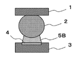
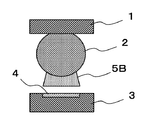
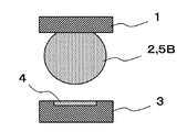
- FIG. 2A, FIG. 2B, and FIG. 2C are explanatory views showing problems due to thinning of the semiconductor package.
- Solder bumps 2 are formed on electrodes (not shown) of the semiconductor package 1.
- a solder paste 5B is applied to the electrode 4 of the substrate 3.
- the solder bump 2 and the solder paste 5B applied to the electrode 4 are in contact with each other.
- the temperature of the substrate 3 and the like is gradually increased at a temperature lower than the temperature at which the solder alloy melts. Due to the thinning of the semiconductor package 1, the semiconductor package 1 warps in a low temperature range of about 120 ° C. to 150 ° C. in a low temperature range than the main active temperature range of the flux.
- Warpage has occurred in the entire semiconductor package 1, and in particular, at the end portion of the component where warpage is particularly large, as shown in FIG. 2B, the solder paste 5 ⁇ / b> B is peeled from the electrode 4 in a state of adhering to the solder bump 2.
- An event is seen.
- the solder paste The solder alloy of 5B is melted, and the solder bump 2 and the solder alloy in the solder paste 5B are fused.
- solder paste 5B Since the solder paste 5B is peeled off from the electrode 4 in this way, the solder paste 5B and the electrode 4 being melted at the time of main heating do not have sufficient contact area or time for solder bonding, or cannot be contacted, The metal oxide film on the surface of the electrode 4 and the activator component in the flux cannot sufficiently react, and the metal oxide film on the surface of the electrode 4 cannot be removed.
- the present invention has been made to solve such a problem.
- the solder paste particularly focuses on the warpage of parts generated in a lower temperature range than the main active temperature range of the flux.
- An object of the present invention is to provide a solder paste flux and a solder paste that can suppress the peeling from the electrode.
- the present invention includes a rosin, a glycol ether solvent, an organic acid, a thixotropic agent, a halogen compound, and an imidazole compound, and the halogen compound is either an amine hydrohalide or an organic halogen compound, or a combination thereof.
- the addition amount of the amine hydrohalide is 0 wt% or more and 2.5 wt%
- the addition amount of the organic halogen compound is 0 wt% or more and 4 wt%.
- the addition amount of the amine hydrohalide when the addition amount of the amine hydrohalide is in the range of 0% by weight or more and less than 0.02% by weight, the addition amount of the organic halogen compound except for the range of 0% by weight or more and less than 0.1% by weight, When the addition amount of the organic halogen compound is 0% by weight or more and less than 0.1% by weight, the addition amount of the amine hydrohalide excludes the range of 0% by weight or more and less than 0.02% by weight.
- the amount of amine hydrohalide added is X (wt%) and the amount of organic halogen compound added is Y (wt%).
- the amount of the organic halogen compound added is in a range satisfying the formula (1), and the amount of the imidazole compound added is 0.1 wt% to 10 wt%.
- An amine hydrogen halide salt or an organic halogen compound is added as an activator that reacts with the metal oxide film in a predetermined low temperature range to remove the metal oxide film.
- the imidazole compound is added as an activator that reacts with the metal oxide film in a predetermined low temperature range to remove the metal oxide film, and is added as imidazole, 2-ethyl-4-methylimidazole, 4-methyl-2-phenylimidazole, 2 -Phenylimidazole, 2-ethylimidazole, 2-methylimidazole, or a combination thereof is preferable.
- the present invention provides a solder paste in which a flux and a solder alloy powder are mixed.
- the flux includes rosin, glycol ether solvent, organic acid, thixotropic agent, halogen compound, and imidazole compound.
- the addition amount of the amine hydrohalide salt is 0 to 2.5% by weight
- the addition amount of the organic halogen compound is 0% by weight More than 4% by weight.
- the addition amount of the amine hydrohalide when the addition amount of the amine hydrohalide is in the range of 0% by weight or more and less than 0.02% by weight, the addition amount of the organic halogen compound except for the range of 0% by weight or more and less than 0.1% by weight, When the addition amount of the organic halogen compound is 0% by weight or more and less than 0.1% by weight, the addition amount of the amine hydrohalide excludes the range of 0% by weight or more and less than 0.02% by weight. As described above, when the above range is simply expressed, when the addition amount of the amine hydrohalide salt is X (wt%) and the addition amount of the organic halogen compound is Y (wt%), the amine hydrogen halide is added.
- the flux for solder paste is such that the addition amount of the acid salt and the addition amount of the organic halogen compound satisfy the formula (1), and the addition amount of the imidazole compound is 0.1 wt% to 10 wt%.
- the activator component in the flux reacts with the oxide on the metal surface in a low temperature range where no reaction occurs between the solder alloy in the solder paste and the flux, and the metal oxide film becomes Removed. If the metal oxide film can be removed in such a low temperature range, the adhesion between the metal powders can be increased, and the solder paste can be prevented from being peeled off from the object to be joined even when stress due to warpage of the substrate is applied.
- the flux of the present embodiment includes a halogen compound, an imidazole compound, an organic acid, rosin, a solvent, and a thixotropic agent.
- the flux of the present embodiment is mixed with solder alloy powder to produce a solder paste.
- halogen compound examples include amine hydrohalides and organic halogen compounds.
- amine hydrohalide compound examples include ethylamine, diethylamine, dibutylamine, tributylamine, isopropylamine, diphenylguanidine, cyclohexylamine, and aniline.
- hydrohalic acid examples include hydrochloric acid, hydrobromic acid, and hydroiodic acid.
- organic halogen compounds examples include 1-bromo-2-butanol, 1-bromo-2-propanol, 3-bromo-1-propanol, 3-bromo-1,2-propanediol, and 1,4-dibromo-2-butanol 1,3-dibromo-2-propanol, 2,3-dibromo-1-propanol, 2,3-dibromo-1,4-butanediol, 2,3-dibromo-2-butene-1,4diol, etc. Can be mentioned.
- the addition amount of the halogen compound was determined as follows.
- the halogen compound was any one of the above-described amine hydrohalides and organic halogen compounds, or a combination thereof.
- the addition amount of the amine hydrohalide is X (wt%) and the addition amount of the organic halogen compound is Y (wt%)
- the addition amount of the amine hydrohalide and the addition amount of the organic halogen compound are ( 1) It was set as the range which satisfy
- an amine compound is added to the flux as an activator that reacts with the metal oxide film in a predetermined low temperature range to remove the metal oxide film.
- the amine compound to be added as the activator is preferably an imidazole compound, such as imidazole, 2-ethyl-4-methylimidazole, 4-methyl-2-phenylimidazole, 2-phenylimidazole, 2-ethylimidazole, 2- Any of methylimidazole or a combination thereof is preferable.
- the amount of imidazole compound added is set to 0.1 to 10% by weight.
- Rosin protects activator components such as halogen compounds and imidazole compounds from heat and suppresses volatilization of the activator components.
- activator components such as halogen compounds and imidazole compounds
- examples of the rosin include hydrogenated rosin, acid-modified rosin, polymerized rosin, and rosin ester.
- Solvent dissolves solid content in flux.
- the solvent is selected from generally known glycol ether compounds. In order to efficiently bring about the action of the activator, it is preferable that it does not volatilize in a low temperature range of 120 ° C. to 150 ° C. When the solvent volatilizes, the fluidity of the flux deteriorates, making it difficult to spread the action of the activator over the entire metal powder. Therefore, the boiling point is preferably 200 ° C. or higher, and more preferably 240 ° C. or higher.
- Thixo drugs are added to impart thixotropy.
- thixotropic agents include higher fatty acid amides, higher fatty acid esters, castor oil and the like.
- Organic acid is added as an activator component in the flux.
- the organic acid is preferably a room temperature solid organic acid such as adipic acid, suberic acid, or sebacic acid.
- solvents other than glycol ethers, antioxidants, surfactants, antifoaming agents, coloring agents, and the like may be appropriately added as long as the performance of the flux is not impaired.
- the organic acid was added at a normal preheating temperature of 150 ° C. or more to remove the solder alloy and the oxide film to be soldered, and the addition amount was 1 wt% to 10 wt%.
- Rosin protects activator components such as halogen compounds and amine compounds from heat and suppresses volatilization of the activator components.
- the amount of rosin added was 40% to 60% by weight.
- the solvent dissolves the solid components in the flux.
- the amount of the solvent added was 25% to 35% by weight.
- the thixotropic agent imparts viscosity to the solder paste.
- the addition amount of the thixotropic agent was 5 to 10% by weight.
- the solder paste of the present embodiment is generated by mixing the above-described flux and solder alloy powder.
- the solder paste in this example is produced by mixing a solder alloy powder whose composition is Sn-3Ag-0.5Cu (each numerical value is wt%) and a flux.
- the present invention is not limited to this solder alloy.
- the fluxes of Examples and Comparative Examples were prepared with the compositions shown in the following table, and solder pastes were prepared using the fluxes of Examples and Comparative Examples, and the solder paste peeling prevention effect was verified.
- the composition ratios in Tables 1 to 3 are weight% in the flux composition.
- amine hydrohalides were selected as the halogen compounds and added in the ratios shown in Table 1 below.
- the hydrohalic acid was hydrogen bromide (HBr), and diphenylguanidine, diethylamine, and isopropylamine were selected as amine compounds that react with hydrohalic acid to form salts.
- imidazole compounds such as imidazole, 2-ethyl-4-methylimidazole, 4-methyl-2-phenylimidazole, 2-phenylimidazole, 2-ethylimidazole, and 2-methylimidazole are used. Were added at the ratios shown in Table 1 below.
- the organic halogen compound is not included, the addition amount of the amine hydrohalide is less than 0.02% by weight, and the comparative example 1 does not include the imidazole compound, the halogen compound is not included, and the addition amount of the imidazole compound is
- Comparative Example 3 of less than 0.1% by weight, the solder paste adhered to the solder balls and peeled from the copper plate.
- the addition amount of an amine hydrohalide salt does not contain an organic halogen compound, and the addition amount of an amine hydrohalide salt exceeds 2.5% by weight, and does not contain an imidazole compound.
- Comparative Example 4 exceeding 10% by weight, a tendency of thickening was observed by continuous viscosity measurement.
- Examples 14 to 25 an organic halogen compound was selected as the halogen compound, and 2,3-dibromo-1,4-butanediol and 2,3-dibromo-2-butene-1,4-diol were Were added at the ratio shown in Table 2.
- imidazole compounds such as imidazole, 2-ethyl-4-methylimidazole, 4-methyl-2-phenylimidazole, 2-phenylimidazole, 2-ethylimidazole, and 2-methylimidazole were used as imidazole compounds. Were added at the ratios shown in Table 2 below.
- Example 14 to Example 25 to which was added the solder paste remained on the copper plate.
- Comparative Example 5 that does not contain an amine hydrohalide, does not contain an organic halogen compound, and does not contain an imidazole compound, the solder paste adheres to the solder balls, Peeled off.
- Comparative Example 6 which does not contain an amine hydrohalide salt, the addition amount of the organic halogen compound exceeds 4% by weight, and does not contain an imidazole compound, a tendency of thickening was observed by continuous viscosity measurement.
- the amount of amine hydrohalide added is 0.02% to 2.5% by weight, and the amount of organic halogen compound added is 0.1% to 4% by weight.
- the amount of amine hydrohalide added is in the range of 0.02 wt% to 2.5 wt%, and the amount of organic halogen compound added is in the range of 0.1 wt% to 4 wt%. Even in Comparative Examples 7 to 9, there was a tendency for thickening by continuous viscosity measurement.
- the amount of amine hydrohalide added is in the range of 0.02 wt% to 2.5 wt%, and the amount of organic halogen compound added is in the range of 0.1 wt% to 4 wt%.
- the addition amount of the amine hydrohalide is X (wt%) and the addition amount of the organic halogen compound is Y (wt%)
- the addition amount of the amine hydrohalide and the addition of the organic halogen compound The amount is an amount that satisfies the formula (1).
- the addition amount of the amine hydrohalide is not less than 0.02 wt% and not more than 2.5 wt%, and the addition amount of the organic halogen compound is not more than 0.1 wt% and not more than 4 wt%. Even if it exists, it was the result which satisfied both the peeling prevention effect and the continuous viscosity measurement. This is because if either one of the amine hydrohalide or the organic halogen compound is added in an amount capable of obtaining an anti-peeling effect alone, the other may be added in an amount where the anti-peeling effect was not obtained alone. Indicates that there is no problem. However, in both cases, the prevention effect is expected to be low at an addition amount that was not able to obtain the peeling prevention effect alone.
- the activator component in the flux reacts with the oxide on the metal surface and the metal oxide film is removed in the low temperature range where there is usually no reaction between the solder alloy in the solder paste and the flux. It was found that the adhesion between the metal powders in the solder paste increased and remained on the substrate. Due to this increase in holding power, it is possible to suppress the solder paste from peeling off from the electrode even when stress due to warping of the substrate is applied.
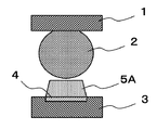
- FIG. 1A, FIG. 1B, and FIG. 1C are explanatory views showing an example of the effect of the flux according to the present embodiment.
- Solder bumps 2 are formed on electrodes (not shown) of the semiconductor package 1. Further, a solder paste 5 ⁇ / b> A is applied to the electrode 4 of the substrate 3. As shown in FIG. 1A, in the step before reflow, the solder bump 2 and the solder paste 5A applied to the electrode 4 are in contact with each other.
- the temperature of the substrate 3 and the like is gradually increased at a temperature lower than the temperature at which the solder alloy melts. Due to the thinning of the semiconductor package 1, the semiconductor package 1 warps in a low temperature range of about 120 ° C. to 150 ° C. lower than the main active temperature range of the flux.
- the solder paste 5A does not peel from the electrode 4 as shown in FIG. 1B in the solder paste 5A in which the flux and the solder alloy of the present embodiment are mixed.
- the metal paste film on the surface of the electrode 4 can be removed because the solder paste 5A does not peel from the electrode 4.
- the solder alloy in the solder paste 5A is melted, the semiconductor package 1 supported on the substrate 3 by the solder paste 5A is lowered. As the semiconductor package 1 descends, the solder bumps 2 of the semiconductor package 1 separated by warping of the semiconductor package 1 and the solder paste 5A applied to the electrodes 4 come into contact.
- the volatilization of the activator component in the flux is suppressed by rosin, and when the solder bump 2 of the semiconductor package 1 and the solder paste 5A applied to the electrode 4 come into contact again, the surface of the solder bump 2 is oxidized with metal. The film is removed.
- solder bump 2 and the solder alloy in the solder paste 5A are fused. Therefore, even if the semiconductor package 1 is warped during the reflow process, the solder bumps 2 of the semiconductor package 1 and the electrodes 4 of the substrate 3 are electrically joined with the solder alloy.
- the present invention is applied to soldering of electronic parts to which BGA is applied.
Landscapes
- Engineering & Computer Science (AREA)
- Mechanical Engineering (AREA)
- General Engineering & Computer Science (AREA)
- Electric Connection Of Electric Components To Printed Circuits (AREA)
Priority Applications (5)
| Application Number | Priority Date | Filing Date | Title |
|---|---|---|---|
| US15/526,051 US20170304961A1 (en) | 2014-11-12 | 2015-11-06 | Solder Paste and Solder Joint |
| EP15859026.5A EP3219433A4 (en) | 2014-11-12 | 2015-11-06 | Flux for solder paste, solder paste, and joined body |
| CN201580061775.2A CN107000133A (zh) | 2014-11-12 | 2015-11-06 | 焊膏用助焊剂、焊膏及钎焊接合体 |
| MYPI2017000704A MY183244A (en) | 2014-11-12 | 2015-11-06 | Solder paste and solder joint |
| PH1/2017/500879A PH12017500879B1 (en) | 2014-11-12 | 2015-11-06 | Solder paste and solder joint |
Applications Claiming Priority (2)
| Application Number | Priority Date | Filing Date | Title |
|---|---|---|---|
| JP2014229886A JP6405920B2 (ja) | 2014-11-12 | 2014-11-12 | ソルダペースト用フラックス、ソルダペースト及びはんだ接合体 |
| JP2014-229886 | 2014-11-12 |
Publications (1)
| Publication Number | Publication Date |
|---|---|
| WO2016076220A1 true WO2016076220A1 (ja) | 2016-05-19 |
Family
ID=55954307
Family Applications (1)
| Application Number | Title | Priority Date | Filing Date |
|---|---|---|---|
| PCT/JP2015/081308 Ceased WO2016076220A1 (ja) | 2014-11-12 | 2015-11-06 | ソルダペースト用フラックス、ソルダペースト及びはんだ接合体 |
Country Status (7)
| Country | Link |
|---|---|
| US (1) | US20170304961A1 (enExample) |
| EP (1) | EP3219433A4 (enExample) |
| JP (1) | JP6405920B2 (enExample) |
| CN (1) | CN107000133A (enExample) |
| MY (1) | MY183244A (enExample) |
| PH (1) | PH12017500879B1 (enExample) |
| WO (1) | WO2016076220A1 (enExample) |
Cited By (1)
| Publication number | Priority date | Publication date | Assignee | Title |
|---|---|---|---|---|
| JP2020192559A (ja) * | 2019-05-27 | 2020-12-03 | 千住金属工業株式会社 | はんだペースト及びはんだペースト用フラックス |
Families Citing this family (16)
| Publication number | Priority date | Publication date | Assignee | Title |
|---|---|---|---|---|
| US10319527B2 (en) | 2017-04-04 | 2019-06-11 | Samsung Electro-Mechanics Co., Ltd. | Multilayer capacitor |
| JP6528102B2 (ja) | 2017-07-03 | 2019-06-12 | 株式会社弘輝 | フラックス及びはんだ材料 |
| JP6390989B1 (ja) * | 2017-11-24 | 2018-09-19 | 千住金属工業株式会社 | フラックス及びソルダペースト |
| JP6617793B2 (ja) | 2018-06-01 | 2019-12-11 | 千住金属工業株式会社 | ソルダペースト用フラックス及びソルダペースト |
| JP6536730B1 (ja) * | 2018-08-10 | 2019-07-03 | 千住金属工業株式会社 | フラックス及びはんだペースト |
| JP7517669B2 (ja) * | 2019-06-27 | 2024-07-17 | 株式会社弘輝 | フラックス及びソルダペースト |
| CN111001965B (zh) * | 2019-10-28 | 2022-03-11 | 东莞市吉田焊接材料有限公司 | 一种有铅锡膏助焊剂及其制备方法与锡膏 |
| JP6795777B1 (ja) * | 2020-03-27 | 2020-12-02 | 千住金属工業株式会社 | 洗浄用フラックス及び洗浄用ソルダペースト |
| JP7161510B2 (ja) * | 2020-09-15 | 2022-10-26 | 株式会社タムラ製作所 | はんだ組成物および電子基板 |
| CN112951730B (zh) * | 2021-01-26 | 2024-03-29 | 北京遥感设备研究所 | 一种基板三维堆叠工艺方法 |
| JP7328311B2 (ja) * | 2021-03-12 | 2023-08-16 | 千住金属工業株式会社 | フラックスおよび電子デバイスの製造方法 |
| WO2022191227A1 (ja) * | 2021-03-12 | 2022-09-15 | 千住金属工業株式会社 | フラックスおよび電子デバイスの製造方法 |
| CN116981541B (zh) * | 2021-03-12 | 2024-11-19 | 千住金属工业株式会社 | 助焊剂和电子设备的制造方法 |
| WO2022191226A1 (ja) * | 2021-03-12 | 2022-09-15 | 千住金属工業株式会社 | フラックスおよび電子デバイスの製造方法 |
| CN117042914B (zh) * | 2021-03-12 | 2024-11-19 | 千住金属工业株式会社 | 助焊剂和电子设备的制造方法 |
| JP7054035B1 (ja) * | 2021-06-09 | 2022-04-13 | 千住金属工業株式会社 | フラックス及びソルダペースト |
Citations (6)
| Publication number | Priority date | Publication date | Assignee | Title |
|---|---|---|---|---|
| JP2002086292A (ja) * | 2000-02-08 | 2002-03-26 | Showa Denko Kk | ハンダペースト |
| JP2003225795A (ja) * | 2002-01-30 | 2003-08-12 | Showa Denko Kk | ハンダ付け用フラックスおよびハンダペースト |
| JP2005059028A (ja) * | 2003-08-08 | 2005-03-10 | Toshiba Corp | 熱硬化性フラックス及びはんだペースト |
| JP2014036985A (ja) * | 2012-08-16 | 2014-02-27 | Tamura Seisakusho Co Ltd | はんだ組成物およびそれを用いたプリント配線基板 |
| JP2014117737A (ja) * | 2012-12-18 | 2014-06-30 | Nippon Handa Kk | ソルダペースト及びはんだ付け実装方法 |
| JP2014144473A (ja) * | 2013-01-29 | 2014-08-14 | Tamura Seisakusho Co Ltd | フラックスおよびソルダペースト |
Family Cites Families (4)
| Publication number | Priority date | Publication date | Assignee | Title |
|---|---|---|---|---|
| JPH05392A (ja) * | 1991-06-18 | 1993-01-08 | Metsuku Kk | はんだ付け用フラツクス及びクリームはんだ |
| JP3398025B2 (ja) * | 1997-10-01 | 2003-04-21 | 三洋電機株式会社 | 液晶表示装置 |
| US20010042779A1 (en) * | 2000-02-08 | 2001-11-22 | Hitoshi Amita | Solder paste |
| US8961709B1 (en) * | 2004-03-09 | 2015-02-24 | Senju Metal Industry Co., Ltd. | Solder paste |
-
2014
- 2014-11-12 JP JP2014229886A patent/JP6405920B2/ja active Active
-
2015
- 2015-11-06 EP EP15859026.5A patent/EP3219433A4/en not_active Withdrawn
- 2015-11-06 CN CN201580061775.2A patent/CN107000133A/zh active Pending
- 2015-11-06 MY MYPI2017000704A patent/MY183244A/en unknown
- 2015-11-06 WO PCT/JP2015/081308 patent/WO2016076220A1/ja not_active Ceased
- 2015-11-06 US US15/526,051 patent/US20170304961A1/en not_active Abandoned
- 2015-11-06 PH PH1/2017/500879A patent/PH12017500879B1/en unknown
Patent Citations (6)
| Publication number | Priority date | Publication date | Assignee | Title |
|---|---|---|---|---|
| JP2002086292A (ja) * | 2000-02-08 | 2002-03-26 | Showa Denko Kk | ハンダペースト |
| JP2003225795A (ja) * | 2002-01-30 | 2003-08-12 | Showa Denko Kk | ハンダ付け用フラックスおよびハンダペースト |
| JP2005059028A (ja) * | 2003-08-08 | 2005-03-10 | Toshiba Corp | 熱硬化性フラックス及びはんだペースト |
| JP2014036985A (ja) * | 2012-08-16 | 2014-02-27 | Tamura Seisakusho Co Ltd | はんだ組成物およびそれを用いたプリント配線基板 |
| JP2014117737A (ja) * | 2012-12-18 | 2014-06-30 | Nippon Handa Kk | ソルダペースト及びはんだ付け実装方法 |
| JP2014144473A (ja) * | 2013-01-29 | 2014-08-14 | Tamura Seisakusho Co Ltd | フラックスおよびソルダペースト |
Non-Patent Citations (1)
| Title |
|---|
| See also references of EP3219433A4 * |
Cited By (1)
| Publication number | Priority date | Publication date | Assignee | Title |
|---|---|---|---|---|
| JP2020192559A (ja) * | 2019-05-27 | 2020-12-03 | 千住金属工業株式会社 | はんだペースト及びはんだペースト用フラックス |
Also Published As
| Publication number | Publication date |
|---|---|
| JP2016093816A (ja) | 2016-05-26 |
| US20170304961A1 (en) | 2017-10-26 |
| PH12017500879B1 (en) | 2023-07-05 |
| CN107000133A (zh) | 2017-08-01 |
| JP6405920B2 (ja) | 2018-10-17 |
| PH12017500879A1 (en) | 2017-11-06 |
| EP3219433A1 (en) | 2017-09-20 |
| MY183244A (en) | 2021-02-18 |
| EP3219433A4 (en) | 2018-06-13 |
Similar Documents
| Publication | Publication Date | Title |
|---|---|---|
| JP6405920B2 (ja) | ソルダペースト用フラックス、ソルダペースト及びはんだ接合体 | |
| JP5093766B2 (ja) | 導電性ボール等搭載半導体パッケージ基板の製造方法 | |
| JP6528102B2 (ja) | フラックス及びはんだ材料 | |
| JP6027426B2 (ja) | ソルダペースト及びはんだ付け実装方法 | |
| TWI681953B (zh) | 助焊劑 | |
| WO2019171978A1 (ja) | はんだ合金、はんだペースト、はんだボール、やに入りはんだおよびはんだ継手 | |
| JPWO2013132942A1 (ja) | 接合方法、接合構造体およびその製造方法 | |
| TWI636140B (zh) | 焊料凸塊之形成方法及焊料球固定用焊料膏 | |
| JP6383544B2 (ja) | はんだ付け用フラックス組成物およびそれを用いた電子基板の製造方法 | |
| JP6423840B2 (ja) | フラックス組成物及びソルダーペースト | |
| JP6222415B1 (ja) | フラックス | |
| JP5160576B2 (ja) | ソルダペーストと、これを用いたピングリッドアレイパッケージ用基板及びピングリッドアレイパッケージ、並びにピングリッドアレイパッケージ用基板の製造方法 | |
| TW201607992A (zh) | 助焊劑組成物 | |
| JP4008799B2 (ja) | 無鉛はんだペースト組成物およびはんだ付け方法 | |
| JP2021102231A (ja) | 無残渣フラックス組成物及びソルダペースト | |
| JP6917506B1 (ja) | フラックス、ソルダペースト、電子回路実装基板及び電子制御装置 | |
| CN103476540A (zh) | 焊料合金 | |
| JP2005297011A (ja) | ソルダーペーストおよび半田付け物品 | |
| JP2006000909A (ja) | はんだ材料および該はんだ材料を用いてはんだ付けされた電子部品 | |
| JP3824901B2 (ja) | ソルダペースト | |
| JP2005199289A (ja) | はんだペースト、半導体電子部品用バンプ、半導体電子部品及び半導体電子部品の実装方法 | |
| JP2000271781A (ja) | ソルダーペースト | |
| JP2017148862A (ja) | はんだペースト | |
| CN107405729A (zh) | 焊膏 |
Legal Events
| Date | Code | Title | Description |
|---|---|---|---|
| 121 | Ep: the epo has been informed by wipo that ep was designated in this application |
Ref document number: 15859026 Country of ref document: EP Kind code of ref document: A1 |
|
| DPE1 | Request for preliminary examination filed after expiration of 19th month from priority date (pct application filed from 20040101) | ||
| WWE | Wipo information: entry into national phase |
Ref document number: 15526051 Country of ref document: US |
|
| NENP | Non-entry into the national phase |
Ref country code: DE |
|
| REEP | Request for entry into the european phase |
Ref document number: 2015859026 Country of ref document: EP |