WO2016076220A1 - ソルダペースト用フラックス、ソルダペースト及びはんだ接合体 - Google Patents
ソルダペースト用フラックス、ソルダペースト及びはんだ接合体 Download PDFInfo
- Publication number
- WO2016076220A1 WO2016076220A1 PCT/JP2015/081308 JP2015081308W WO2016076220A1 WO 2016076220 A1 WO2016076220 A1 WO 2016076220A1 JP 2015081308 W JP2015081308 W JP 2015081308W WO 2016076220 A1 WO2016076220 A1 WO 2016076220A1
- Authority
- WO
- WIPO (PCT)
- Prior art keywords
- solder paste
- addition amount
- solder
- compound
- flux
- Prior art date
Links
- 229910000679 solder Inorganic materials 0.000 title claims abstract description 138
- 230000004907 flux Effects 0.000 title claims abstract description 50
- RAXXELZNTBOGNW-UHFFFAOYSA-N imidazole Natural products C1=CNC=N1 RAXXELZNTBOGNW-UHFFFAOYSA-N 0.000 claims abstract description 59
- 150000001412 amines Chemical class 0.000 claims abstract description 45
- 150000002896 organic halogen compounds Chemical class 0.000 claims abstract description 44
- -1 imidazole compound Chemical class 0.000 claims abstract description 30
- 150000002366 halogen compounds Chemical class 0.000 claims abstract description 20
- RSWGJHLUYNHPMX-UHFFFAOYSA-N Abietic-Saeure Natural products C12CCC(C(C)C)=CC2=CCC2C1(C)CCCC2(C)C(O)=O RSWGJHLUYNHPMX-UHFFFAOYSA-N 0.000 claims abstract description 14
- KHPCPRHQVVSZAH-HUOMCSJISA-N Rosin Natural products O(C/C=C/c1ccccc1)[C@H]1[C@H](O)[C@@H](O)[C@@H](O)[C@@H](CO)O1 KHPCPRHQVVSZAH-HUOMCSJISA-N 0.000 claims abstract description 14
- KHPCPRHQVVSZAH-UHFFFAOYSA-N trans-cinnamyl beta-D-glucopyranoside Natural products OC1C(O)C(O)C(CO)OC1OCC=CC1=CC=CC=C1 KHPCPRHQVVSZAH-UHFFFAOYSA-N 0.000 claims abstract description 14
- 239000013008 thixotropic agent Substances 0.000 claims abstract description 8
- MTHSVFCYNBDYFN-UHFFFAOYSA-N diethylene glycol Chemical compound OCCOCCO MTHSVFCYNBDYFN-UHFFFAOYSA-N 0.000 claims abstract description 5
- 239000004210 ether based solvent Substances 0.000 claims abstract 2
- 229910045601 alloy Inorganic materials 0.000 claims description 32
- 239000000956 alloy Substances 0.000 claims description 32
- 239000000843 powder Substances 0.000 claims description 12
- 150000003839 salts Chemical class 0.000 claims description 12
- 150000007524 organic acids Chemical class 0.000 claims description 8
- 239000002253 acid Substances 0.000 claims description 6
- PQAMFDRRWURCFQ-UHFFFAOYSA-N 2-ethyl-1h-imidazole Chemical compound CCC1=NC=CN1 PQAMFDRRWURCFQ-UHFFFAOYSA-N 0.000 claims description 5
- LXBGSDVWAMZHDD-UHFFFAOYSA-N 2-methyl-1h-imidazole Chemical compound CC1=NC=CN1 LXBGSDVWAMZHDD-UHFFFAOYSA-N 0.000 claims description 5
- ZCUJYXPAKHMBAZ-UHFFFAOYSA-N 2-phenyl-1h-imidazole Chemical compound C1=CNC(C=2C=CC=CC=2)=N1 ZCUJYXPAKHMBAZ-UHFFFAOYSA-N 0.000 claims description 5
- TYOXIFXYEIILLY-UHFFFAOYSA-N 5-methyl-2-phenyl-1h-imidazole Chemical compound N1C(C)=CN=C1C1=CC=CC=C1 TYOXIFXYEIILLY-UHFFFAOYSA-N 0.000 claims description 5
- ULKLGIFJWFIQFF-UHFFFAOYSA-N 5K8XI641G3 Chemical compound CCC1=NC=C(C)N1 ULKLGIFJWFIQFF-UHFFFAOYSA-N 0.000 claims description 5
- 150000002460 imidazoles Chemical class 0.000 claims description 5
- OWRCNXZUPFZXOS-UHFFFAOYSA-N 1,3-diphenylguanidine Chemical compound C=1C=CC=CC=1NC(=N)NC1=CC=CC=C1 OWRCNXZUPFZXOS-UHFFFAOYSA-N 0.000 claims description 4
- OXYNQEOLHRWEPE-UHFFFAOYSA-N 2,3-dibromobutane-1,4-diol Chemical compound OCC(Br)C(Br)CO OXYNQEOLHRWEPE-UHFFFAOYSA-N 0.000 claims description 4
- PAYRUJLWNCNPSJ-UHFFFAOYSA-N Aniline Chemical compound NC1=CC=CC=C1 PAYRUJLWNCNPSJ-UHFFFAOYSA-N 0.000 claims description 4
- QUSNBJAOOMFDIB-UHFFFAOYSA-N Ethylamine Chemical compound CCN QUSNBJAOOMFDIB-UHFFFAOYSA-N 0.000 claims description 4
- VEXZGXHMUGYJMC-UHFFFAOYSA-N Hydrochloric acid Chemical compound Cl VEXZGXHMUGYJMC-UHFFFAOYSA-N 0.000 claims description 4
- PAFZNILMFXTMIY-UHFFFAOYSA-N cyclohexylamine Chemical compound NC1CCCCC1 PAFZNILMFXTMIY-UHFFFAOYSA-N 0.000 claims description 4
- JQVDAXLFBXTEQA-UHFFFAOYSA-N dibutylamine Chemical compound CCCCNCCCC JQVDAXLFBXTEQA-UHFFFAOYSA-N 0.000 claims description 4
- MELXIJRBKWTTJH-ONEGZZNKSA-N (e)-2,3-dibromobut-2-ene-1,4-diol Chemical compound OC\C(Br)=C(/Br)CO MELXIJRBKWTTJH-ONEGZZNKSA-N 0.000 claims description 3
- HPNMFZURTQLUMO-UHFFFAOYSA-N diethylamine Chemical compound CCNCC HPNMFZURTQLUMO-UHFFFAOYSA-N 0.000 claims description 3
- JJWLVOIRVHMVIS-UHFFFAOYSA-N isopropylamine Chemical compound CC(C)N JJWLVOIRVHMVIS-UHFFFAOYSA-N 0.000 claims description 3
- WEGOLYBUWCMMMY-UHFFFAOYSA-N 1-bromo-2-propanol Chemical compound CC(O)CBr WEGOLYBUWCMMMY-UHFFFAOYSA-N 0.000 claims description 2
- DMRXISNUOWIOKV-UHFFFAOYSA-N 1-bromobutan-2-ol Chemical compound CCC(O)CBr DMRXISNUOWIOKV-UHFFFAOYSA-N 0.000 claims description 2
- QWVCIORZLNBIIC-UHFFFAOYSA-N 2,3-dibromopropan-1-ol Chemical compound OCC(Br)CBr QWVCIORZLNBIIC-UHFFFAOYSA-N 0.000 claims description 2
- RQFUZUMFPRMVDX-UHFFFAOYSA-N 3-Bromo-1-propanol Chemical compound OCCCBr RQFUZUMFPRMVDX-UHFFFAOYSA-N 0.000 claims description 2
- BMYNFMYTOJXKLE-UHFFFAOYSA-N 3-azaniumyl-2-hydroxypropanoate Chemical compound NCC(O)C(O)=O BMYNFMYTOJXKLE-UHFFFAOYSA-N 0.000 claims description 2
- SIBFQOUHOCRXDL-UHFFFAOYSA-N 3-bromopropane-1,2-diol Chemical compound OCC(O)CBr SIBFQOUHOCRXDL-UHFFFAOYSA-N 0.000 claims description 2
- JPHZWGQRRVQXRT-UHFFFAOYSA-N BrCC(CBr)O.BrCC(CCBr)O Chemical compound BrCC(CBr)O.BrCC(CCBr)O JPHZWGQRRVQXRT-UHFFFAOYSA-N 0.000 claims description 2
- XMBWDFGMSWQBCA-UHFFFAOYSA-N hydrogen iodide Chemical compound I XMBWDFGMSWQBCA-UHFFFAOYSA-N 0.000 claims description 2
- 229940071870 hydroiodic acid Drugs 0.000 claims description 2
- IMFACGCPASFAPR-UHFFFAOYSA-N tributylamine Chemical compound CCCCN(CCCC)CCCC IMFACGCPASFAPR-UHFFFAOYSA-N 0.000 claims description 2
- 235000005985 organic acids Nutrition 0.000 claims 1
- 239000004065 semiconductor Substances 0.000 abstract description 38
- 239000003960 organic solvent Substances 0.000 abstract 1
- 239000012190 activator Substances 0.000 description 16
- 230000000694 effects Effects 0.000 description 15
- 239000000758 substrate Substances 0.000 description 15
- 229910044991 metal oxide Inorganic materials 0.000 description 13
- 150000004706 metal oxides Chemical class 0.000 description 13
- 238000010438 heat treatment Methods 0.000 description 12
- 239000002904 solvent Substances 0.000 description 9
- 230000000052 comparative effect Effects 0.000 description 8
- 238000005259 measurement Methods 0.000 description 8
- 239000002184 metal Substances 0.000 description 8
- 229910052751 metal Inorganic materials 0.000 description 8
- RYGMFSIKBFXOCR-UHFFFAOYSA-N Copper Chemical compound [Cu] RYGMFSIKBFXOCR-UHFFFAOYSA-N 0.000 description 6
- 229910052802 copper Inorganic materials 0.000 description 6
- 239000010949 copper Substances 0.000 description 6
- 238000005476 soldering Methods 0.000 description 6
- 239000000155 melt Substances 0.000 description 5
- 239000000203 mixture Substances 0.000 description 5
- 230000002265 prevention Effects 0.000 description 5
- 238000000034 method Methods 0.000 description 4
- 230000008569 process Effects 0.000 description 4
- 230000009467 reduction Effects 0.000 description 4
- CPELXLSAUQHCOX-UHFFFAOYSA-N Hydrogen bromide Chemical compound Br CPELXLSAUQHCOX-UHFFFAOYSA-N 0.000 description 3
- 238000006243 chemical reaction Methods 0.000 description 3
- 239000007787 solid Substances 0.000 description 3
- 230000008719 thickening Effects 0.000 description 3
- 238000012795 verification Methods 0.000 description 3
- 230000009471 action Effects 0.000 description 2
- WNLRTRBMVRJNCN-UHFFFAOYSA-N adipic acid Chemical compound OC(=O)CCCCC(O)=O WNLRTRBMVRJNCN-UHFFFAOYSA-N 0.000 description 2
- 150000001875 compounds Chemical class 0.000 description 2
- 235000014113 dietary fatty acids Nutrition 0.000 description 2
- 238000011156 evaluation Methods 0.000 description 2
- 239000000194 fatty acid Substances 0.000 description 2
- 229930195729 fatty acid Natural products 0.000 description 2
- 229910000039 hydrogen halide Inorganic materials 0.000 description 2
- 239000012433 hydrogen halide Substances 0.000 description 2
- 238000002844 melting Methods 0.000 description 2
- 230000008018 melting Effects 0.000 description 2
- CXMXRPHRNRROMY-UHFFFAOYSA-N sebacic acid Chemical compound OC(=O)CCCCCCCCC(O)=O CXMXRPHRNRROMY-UHFFFAOYSA-N 0.000 description 2
- TYFQFVWCELRYAO-UHFFFAOYSA-N suberic acid Chemical compound OC(=O)CCCCCCC(O)=O TYFQFVWCELRYAO-UHFFFAOYSA-N 0.000 description 2
- 239000000654 additive Substances 0.000 description 1
- 239000001361 adipic acid Substances 0.000 description 1
- 235000011037 adipic acid Nutrition 0.000 description 1
- 239000002518 antifoaming agent Substances 0.000 description 1
- 239000003963 antioxidant agent Substances 0.000 description 1
- 238000009835 boiling Methods 0.000 description 1
- 239000004359 castor oil Substances 0.000 description 1
- 235000019438 castor oil Nutrition 0.000 description 1
- 239000003086 colorant Substances 0.000 description 1
- 239000002131 composite material Substances 0.000 description 1
- 239000003814 drug Substances 0.000 description 1
- 229940079593 drug Drugs 0.000 description 1
- 150000002148 esters Chemical class 0.000 description 1
- LYCAIKOWRPUZTN-UHFFFAOYSA-N ethylene glycol Natural products OCCO LYCAIKOWRPUZTN-UHFFFAOYSA-N 0.000 description 1
- 150000004665 fatty acids Chemical class 0.000 description 1
- ZEMPKEQAKRGZGQ-XOQCFJPHSA-N glycerol triricinoleate Natural products CCCCCC[C@@H](O)CC=CCCCCCCCC(=O)OC[C@@H](COC(=O)CCCCCCCC=CC[C@@H](O)CCCCCC)OC(=O)CCCCCCCC=CC[C@H](O)CCCCCC ZEMPKEQAKRGZGQ-XOQCFJPHSA-N 0.000 description 1
- 229910052736 halogen Inorganic materials 0.000 description 1
- 150000002367 halogens Chemical class 0.000 description 1
- 229910000042 hydrogen bromide Inorganic materials 0.000 description 1
- WGCNASOHLSPBMP-UHFFFAOYSA-N hydroxyacetaldehyde Natural products OCC=O WGCNASOHLSPBMP-UHFFFAOYSA-N 0.000 description 1
- 230000001771 impaired effect Effects 0.000 description 1
- 238000000691 measurement method Methods 0.000 description 1
- XLSZMDLNRCVEIJ-UHFFFAOYSA-N methylimidazole Natural products CC1=CNC=N1 XLSZMDLNRCVEIJ-UHFFFAOYSA-N 0.000 description 1
- 238000010405 reoxidation reaction Methods 0.000 description 1
- 239000011347 resin Substances 0.000 description 1
- 229920005989 resin Polymers 0.000 description 1
- 238000007711 solidification Methods 0.000 description 1
- 230000008023 solidification Effects 0.000 description 1
- 239000004094 surface-active agent Substances 0.000 description 1
- 238000012360 testing method Methods 0.000 description 1
Images


Classifications
-
- B—PERFORMING OPERATIONS; TRANSPORTING
- B23—MACHINE TOOLS; METAL-WORKING NOT OTHERWISE PROVIDED FOR
- B23K—SOLDERING OR UNSOLDERING; WELDING; CLADDING OR PLATING BY SOLDERING OR WELDING; CUTTING BY APPLYING HEAT LOCALLY, e.g. FLAME CUTTING; WORKING BY LASER BEAM
- B23K35/00—Rods, electrodes, materials, or media, for use in soldering, welding, or cutting
- B23K35/22—Rods, electrodes, materials, or media, for use in soldering, welding, or cutting characterised by the composition or nature of the material
- B23K35/36—Selection of non-metallic compositions, e.g. coatings, fluxes; Selection of soldering or welding materials, conjoint with selection of non-metallic compositions, both selections being of interest
- B23K35/362—Selection of compositions of fluxes
-
- B—PERFORMING OPERATIONS; TRANSPORTING
- B23—MACHINE TOOLS; METAL-WORKING NOT OTHERWISE PROVIDED FOR
- B23K—SOLDERING OR UNSOLDERING; WELDING; CLADDING OR PLATING BY SOLDERING OR WELDING; CUTTING BY APPLYING HEAT LOCALLY, e.g. FLAME CUTTING; WORKING BY LASER BEAM
- B23K35/00—Rods, electrodes, materials, or media, for use in soldering, welding, or cutting
- B23K35/22—Rods, electrodes, materials, or media, for use in soldering, welding, or cutting characterised by the composition or nature of the material
- B23K35/36—Selection of non-metallic compositions, e.g. coatings, fluxes; Selection of soldering or welding materials, conjoint with selection of non-metallic compositions, both selections being of interest
- B23K35/3612—Selection of non-metallic compositions, e.g. coatings, fluxes; Selection of soldering or welding materials, conjoint with selection of non-metallic compositions, both selections being of interest with organic compounds as principal constituents
- B23K35/3613—Polymers, e.g. resins
-
- B—PERFORMING OPERATIONS; TRANSPORTING
- B23—MACHINE TOOLS; METAL-WORKING NOT OTHERWISE PROVIDED FOR
- B23K—SOLDERING OR UNSOLDERING; WELDING; CLADDING OR PLATING BY SOLDERING OR WELDING; CUTTING BY APPLYING HEAT LOCALLY, e.g. FLAME CUTTING; WORKING BY LASER BEAM
- B23K35/00—Rods, electrodes, materials, or media, for use in soldering, welding, or cutting
- B23K35/22—Rods, electrodes, materials, or media, for use in soldering, welding, or cutting characterised by the composition or nature of the material
- B23K35/36—Selection of non-metallic compositions, e.g. coatings, fluxes; Selection of soldering or welding materials, conjoint with selection of non-metallic compositions, both selections being of interest
- B23K35/3612—Selection of non-metallic compositions, e.g. coatings, fluxes; Selection of soldering or welding materials, conjoint with selection of non-metallic compositions, both selections being of interest with organic compounds as principal constituents
- B23K35/3616—Halogen compounds
-
- F—MECHANICAL ENGINEERING; LIGHTING; HEATING; WEAPONS; BLASTING
- F16—ENGINEERING ELEMENTS AND UNITS; GENERAL MEASURES FOR PRODUCING AND MAINTAINING EFFECTIVE FUNCTIONING OF MACHINES OR INSTALLATIONS; THERMAL INSULATION IN GENERAL
- F16B—DEVICES FOR FASTENING OR SECURING CONSTRUCTIONAL ELEMENTS OR MACHINE PARTS TOGETHER, e.g. NAILS, BOLTS, CIRCLIPS, CLAMPS, CLIPS OR WEDGES; JOINTS OR JOINTING
- F16B5/00—Joining sheets or plates, e.g. panels, to one another or to strips or bars parallel to them
- F16B5/08—Joining sheets or plates, e.g. panels, to one another or to strips or bars parallel to them by means of welds or the like
Definitions
- the present invention relates to a solder paste flux that is mixed with a solder alloy powder to produce a solder paste, a solder paste in which this flux and a solder alloy powder are mixed, and a solder joint that is joined using this solder paste. About the body.
- the flux used for soldering has the effect of preventing removal of the oxide film and reoxidation of the solder and the soldering target at a temperature lower than the temperature at which the solder alloy melts.
- Solder paste is a composite material obtained by mixing solder alloy powder and flux.
- the solder paste is applied to the soldering part such as the electrodes of the board, the parts are mounted on the soldering part to which the solder paste is applied, and the solder is heated by heating the board in a heating furnace called a reflow furnace.
- Soldering is performed.
- the reflow temperature profile of Sn-3Ag-0.5Cu which is a solder alloy that is widely used at present
- the preheating is performed from the start of heating in the furnace to the melting temperature of the solder alloy, and the melting temperature of the solder alloy is 220. This heating is over °C.
- a temperature range of 150 ° C. or higher is generally used as the main active temperature range of the flux.
- This reflow temperature profile varies depending on the solder alloy.
- An electronic component to which BGA is applied includes, for example, a semiconductor package.
- a semiconductor package a semiconductor chip having electrodes is sealed with a resin.
- Solder bumps are formed on the electrodes of the semiconductor package. The solder bumps are formed by joining solder balls to the electrodes of the semiconductor package.
- a semiconductor package to which BGA is applied is such that each solder bump is placed in alignment with the electrode of the substrate to which the solder paste is applied, and the solder paste, which is melted by heating, and the solder bump and the electrode are joined together. Mounted on.
- a problem with conventional BGA solder joints is the unfusion of solder bumps and solder paste.
- the semiconductor package begins to warp by heating, but in this heating process, the solder alloy in the solder paste melts, so that the semiconductor package supported on the substrate by the solder paste descends and is separated by warping the semiconductor package
- the solder paste and the electrode come into contact again.
- the activator component in the flux is volatilized by heating in the reflow process, the metal oxide film on the surface of the electrode cannot be removed even if the solder paste comes into contact with the electrode in this heating process. Therefore, even if the solder alloy in the solder paste is before solidification, the solder alloy and the electrode in the solder paste are not fused. As a result, poor bonding occurs between the solder bumps of the semiconductor package and the electrodes of the substrate.
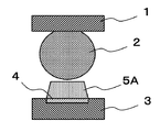
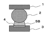
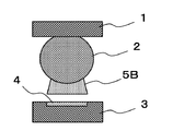
- FIG. 2A, FIG. 2B, and FIG. 2C are explanatory views showing problems due to thinning of the semiconductor package.
- Solder bumps 2 are formed on electrodes (not shown) of the semiconductor package 1.
- a solder paste 5B is applied to the electrode 4 of the substrate 3.
- the solder bump 2 and the solder paste 5B applied to the electrode 4 are in contact with each other.
- the temperature of the substrate 3 and the like is gradually increased at a temperature lower than the temperature at which the solder alloy melts. Due to the thinning of the semiconductor package 1, the semiconductor package 1 warps in a low temperature range of about 120 ° C. to 150 ° C. in a low temperature range than the main active temperature range of the flux.
- Warpage has occurred in the entire semiconductor package 1, and in particular, at the end portion of the component where warpage is particularly large, as shown in FIG. 2B, the solder paste 5 ⁇ / b> B is peeled from the electrode 4 in a state of adhering to the solder bump 2.
- An event is seen.
- the solder paste The solder alloy of 5B is melted, and the solder bump 2 and the solder alloy in the solder paste 5B are fused.
- solder paste 5B Since the solder paste 5B is peeled off from the electrode 4 in this way, the solder paste 5B and the electrode 4 being melted at the time of main heating do not have sufficient contact area or time for solder bonding, or cannot be contacted, The metal oxide film on the surface of the electrode 4 and the activator component in the flux cannot sufficiently react, and the metal oxide film on the surface of the electrode 4 cannot be removed.
- the present invention has been made to solve such a problem.
- the solder paste particularly focuses on the warpage of parts generated in a lower temperature range than the main active temperature range of the flux.
- An object of the present invention is to provide a solder paste flux and a solder paste that can suppress the peeling from the electrode.
- the present invention includes a rosin, a glycol ether solvent, an organic acid, a thixotropic agent, a halogen compound, and an imidazole compound, and the halogen compound is either an amine hydrohalide or an organic halogen compound, or a combination thereof.
- the addition amount of the amine hydrohalide is 0 wt% or more and 2.5 wt%
- the addition amount of the organic halogen compound is 0 wt% or more and 4 wt%.
- the addition amount of the amine hydrohalide when the addition amount of the amine hydrohalide is in the range of 0% by weight or more and less than 0.02% by weight, the addition amount of the organic halogen compound except for the range of 0% by weight or more and less than 0.1% by weight, When the addition amount of the organic halogen compound is 0% by weight or more and less than 0.1% by weight, the addition amount of the amine hydrohalide excludes the range of 0% by weight or more and less than 0.02% by weight.
- the amount of amine hydrohalide added is X (wt%) and the amount of organic halogen compound added is Y (wt%).
- the amount of the organic halogen compound added is in a range satisfying the formula (1), and the amount of the imidazole compound added is 0.1 wt% to 10 wt%.
- An amine hydrogen halide salt or an organic halogen compound is added as an activator that reacts with the metal oxide film in a predetermined low temperature range to remove the metal oxide film.
- the imidazole compound is added as an activator that reacts with the metal oxide film in a predetermined low temperature range to remove the metal oxide film, and is added as imidazole, 2-ethyl-4-methylimidazole, 4-methyl-2-phenylimidazole, 2 -Phenylimidazole, 2-ethylimidazole, 2-methylimidazole, or a combination thereof is preferable.
- the present invention provides a solder paste in which a flux and a solder alloy powder are mixed.
- the flux includes rosin, glycol ether solvent, organic acid, thixotropic agent, halogen compound, and imidazole compound.
- the addition amount of the amine hydrohalide salt is 0 to 2.5% by weight
- the addition amount of the organic halogen compound is 0% by weight More than 4% by weight.
- the addition amount of the amine hydrohalide when the addition amount of the amine hydrohalide is in the range of 0% by weight or more and less than 0.02% by weight, the addition amount of the organic halogen compound except for the range of 0% by weight or more and less than 0.1% by weight, When the addition amount of the organic halogen compound is 0% by weight or more and less than 0.1% by weight, the addition amount of the amine hydrohalide excludes the range of 0% by weight or more and less than 0.02% by weight. As described above, when the above range is simply expressed, when the addition amount of the amine hydrohalide salt is X (wt%) and the addition amount of the organic halogen compound is Y (wt%), the amine hydrogen halide is added.
- the flux for solder paste is such that the addition amount of the acid salt and the addition amount of the organic halogen compound satisfy the formula (1), and the addition amount of the imidazole compound is 0.1 wt% to 10 wt%.
- the activator component in the flux reacts with the oxide on the metal surface in a low temperature range where no reaction occurs between the solder alloy in the solder paste and the flux, and the metal oxide film becomes Removed. If the metal oxide film can be removed in such a low temperature range, the adhesion between the metal powders can be increased, and the solder paste can be prevented from being peeled off from the object to be joined even when stress due to warpage of the substrate is applied.
- the flux of the present embodiment includes a halogen compound, an imidazole compound, an organic acid, rosin, a solvent, and a thixotropic agent.
- the flux of the present embodiment is mixed with solder alloy powder to produce a solder paste.
- halogen compound examples include amine hydrohalides and organic halogen compounds.
- amine hydrohalide compound examples include ethylamine, diethylamine, dibutylamine, tributylamine, isopropylamine, diphenylguanidine, cyclohexylamine, and aniline.
- hydrohalic acid examples include hydrochloric acid, hydrobromic acid, and hydroiodic acid.
- organic halogen compounds examples include 1-bromo-2-butanol, 1-bromo-2-propanol, 3-bromo-1-propanol, 3-bromo-1,2-propanediol, and 1,4-dibromo-2-butanol 1,3-dibromo-2-propanol, 2,3-dibromo-1-propanol, 2,3-dibromo-1,4-butanediol, 2,3-dibromo-2-butene-1,4diol, etc. Can be mentioned.
- the addition amount of the halogen compound was determined as follows.
- the halogen compound was any one of the above-described amine hydrohalides and organic halogen compounds, or a combination thereof.
- the addition amount of the amine hydrohalide is X (wt%) and the addition amount of the organic halogen compound is Y (wt%)
- the addition amount of the amine hydrohalide and the addition amount of the organic halogen compound are ( 1) It was set as the range which satisfy
- an amine compound is added to the flux as an activator that reacts with the metal oxide film in a predetermined low temperature range to remove the metal oxide film.
- the amine compound to be added as the activator is preferably an imidazole compound, such as imidazole, 2-ethyl-4-methylimidazole, 4-methyl-2-phenylimidazole, 2-phenylimidazole, 2-ethylimidazole, 2- Any of methylimidazole or a combination thereof is preferable.
- the amount of imidazole compound added is set to 0.1 to 10% by weight.
- Rosin protects activator components such as halogen compounds and imidazole compounds from heat and suppresses volatilization of the activator components.
- activator components such as halogen compounds and imidazole compounds
- examples of the rosin include hydrogenated rosin, acid-modified rosin, polymerized rosin, and rosin ester.
- Solvent dissolves solid content in flux.
- the solvent is selected from generally known glycol ether compounds. In order to efficiently bring about the action of the activator, it is preferable that it does not volatilize in a low temperature range of 120 ° C. to 150 ° C. When the solvent volatilizes, the fluidity of the flux deteriorates, making it difficult to spread the action of the activator over the entire metal powder. Therefore, the boiling point is preferably 200 ° C. or higher, and more preferably 240 ° C. or higher.
- Thixo drugs are added to impart thixotropy.
- thixotropic agents include higher fatty acid amides, higher fatty acid esters, castor oil and the like.
- Organic acid is added as an activator component in the flux.
- the organic acid is preferably a room temperature solid organic acid such as adipic acid, suberic acid, or sebacic acid.
- solvents other than glycol ethers, antioxidants, surfactants, antifoaming agents, coloring agents, and the like may be appropriately added as long as the performance of the flux is not impaired.
- the organic acid was added at a normal preheating temperature of 150 ° C. or more to remove the solder alloy and the oxide film to be soldered, and the addition amount was 1 wt% to 10 wt%.
- Rosin protects activator components such as halogen compounds and amine compounds from heat and suppresses volatilization of the activator components.
- the amount of rosin added was 40% to 60% by weight.
- the solvent dissolves the solid components in the flux.
- the amount of the solvent added was 25% to 35% by weight.
- the thixotropic agent imparts viscosity to the solder paste.
- the addition amount of the thixotropic agent was 5 to 10% by weight.
- the solder paste of the present embodiment is generated by mixing the above-described flux and solder alloy powder.
- the solder paste in this example is produced by mixing a solder alloy powder whose composition is Sn-3Ag-0.5Cu (each numerical value is wt%) and a flux.
- the present invention is not limited to this solder alloy.
- the fluxes of Examples and Comparative Examples were prepared with the compositions shown in the following table, and solder pastes were prepared using the fluxes of Examples and Comparative Examples, and the solder paste peeling prevention effect was verified.
- the composition ratios in Tables 1 to 3 are weight% in the flux composition.
- amine hydrohalides were selected as the halogen compounds and added in the ratios shown in Table 1 below.
- the hydrohalic acid was hydrogen bromide (HBr), and diphenylguanidine, diethylamine, and isopropylamine were selected as amine compounds that react with hydrohalic acid to form salts.
- imidazole compounds such as imidazole, 2-ethyl-4-methylimidazole, 4-methyl-2-phenylimidazole, 2-phenylimidazole, 2-ethylimidazole, and 2-methylimidazole are used. Were added at the ratios shown in Table 1 below.
- the organic halogen compound is not included, the addition amount of the amine hydrohalide is less than 0.02% by weight, and the comparative example 1 does not include the imidazole compound, the halogen compound is not included, and the addition amount of the imidazole compound is
- Comparative Example 3 of less than 0.1% by weight, the solder paste adhered to the solder balls and peeled from the copper plate.
- the addition amount of an amine hydrohalide salt does not contain an organic halogen compound, and the addition amount of an amine hydrohalide salt exceeds 2.5% by weight, and does not contain an imidazole compound.
- Comparative Example 4 exceeding 10% by weight, a tendency of thickening was observed by continuous viscosity measurement.
- Examples 14 to 25 an organic halogen compound was selected as the halogen compound, and 2,3-dibromo-1,4-butanediol and 2,3-dibromo-2-butene-1,4-diol were Were added at the ratio shown in Table 2.
- imidazole compounds such as imidazole, 2-ethyl-4-methylimidazole, 4-methyl-2-phenylimidazole, 2-phenylimidazole, 2-ethylimidazole, and 2-methylimidazole were used as imidazole compounds. Were added at the ratios shown in Table 2 below.
- Example 14 to Example 25 to which was added the solder paste remained on the copper plate.
- Comparative Example 5 that does not contain an amine hydrohalide, does not contain an organic halogen compound, and does not contain an imidazole compound, the solder paste adheres to the solder balls, Peeled off.
- Comparative Example 6 which does not contain an amine hydrohalide salt, the addition amount of the organic halogen compound exceeds 4% by weight, and does not contain an imidazole compound, a tendency of thickening was observed by continuous viscosity measurement.
- the amount of amine hydrohalide added is 0.02% to 2.5% by weight, and the amount of organic halogen compound added is 0.1% to 4% by weight.
- the amount of amine hydrohalide added is in the range of 0.02 wt% to 2.5 wt%, and the amount of organic halogen compound added is in the range of 0.1 wt% to 4 wt%. Even in Comparative Examples 7 to 9, there was a tendency for thickening by continuous viscosity measurement.
- the amount of amine hydrohalide added is in the range of 0.02 wt% to 2.5 wt%, and the amount of organic halogen compound added is in the range of 0.1 wt% to 4 wt%.
- the addition amount of the amine hydrohalide is X (wt%) and the addition amount of the organic halogen compound is Y (wt%)
- the addition amount of the amine hydrohalide and the addition of the organic halogen compound The amount is an amount that satisfies the formula (1).
- the addition amount of the amine hydrohalide is not less than 0.02 wt% and not more than 2.5 wt%, and the addition amount of the organic halogen compound is not more than 0.1 wt% and not more than 4 wt%. Even if it exists, it was the result which satisfied both the peeling prevention effect and the continuous viscosity measurement. This is because if either one of the amine hydrohalide or the organic halogen compound is added in an amount capable of obtaining an anti-peeling effect alone, the other may be added in an amount where the anti-peeling effect was not obtained alone. Indicates that there is no problem. However, in both cases, the prevention effect is expected to be low at an addition amount that was not able to obtain the peeling prevention effect alone.
- the activator component in the flux reacts with the oxide on the metal surface and the metal oxide film is removed in the low temperature range where there is usually no reaction between the solder alloy in the solder paste and the flux. It was found that the adhesion between the metal powders in the solder paste increased and remained on the substrate. Due to this increase in holding power, it is possible to suppress the solder paste from peeling off from the electrode even when stress due to warping of the substrate is applied.
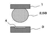
- FIG. 1A, FIG. 1B, and FIG. 1C are explanatory views showing an example of the effect of the flux according to the present embodiment.
- Solder bumps 2 are formed on electrodes (not shown) of the semiconductor package 1. Further, a solder paste 5 ⁇ / b> A is applied to the electrode 4 of the substrate 3. As shown in FIG. 1A, in the step before reflow, the solder bump 2 and the solder paste 5A applied to the electrode 4 are in contact with each other.
- the temperature of the substrate 3 and the like is gradually increased at a temperature lower than the temperature at which the solder alloy melts. Due to the thinning of the semiconductor package 1, the semiconductor package 1 warps in a low temperature range of about 120 ° C. to 150 ° C. lower than the main active temperature range of the flux.
- the solder paste 5A does not peel from the electrode 4 as shown in FIG. 1B in the solder paste 5A in which the flux and the solder alloy of the present embodiment are mixed.
- the metal paste film on the surface of the electrode 4 can be removed because the solder paste 5A does not peel from the electrode 4.
- the solder alloy in the solder paste 5A is melted, the semiconductor package 1 supported on the substrate 3 by the solder paste 5A is lowered. As the semiconductor package 1 descends, the solder bumps 2 of the semiconductor package 1 separated by warping of the semiconductor package 1 and the solder paste 5A applied to the electrodes 4 come into contact.
- the volatilization of the activator component in the flux is suppressed by rosin, and when the solder bump 2 of the semiconductor package 1 and the solder paste 5A applied to the electrode 4 come into contact again, the surface of the solder bump 2 is oxidized with metal. The film is removed.
- solder bump 2 and the solder alloy in the solder paste 5A are fused. Therefore, even if the semiconductor package 1 is warped during the reflow process, the solder bumps 2 of the semiconductor package 1 and the electrodes 4 of the substrate 3 are electrically joined with the solder alloy.
- the present invention is applied to soldering of electronic parts to which BGA is applied.
Landscapes
- Engineering & Computer Science (AREA)
- Mechanical Engineering (AREA)
- General Engineering & Computer Science (AREA)
- Electric Connection Of Electric Components To Printed Circuits (AREA)
Abstract
BGAなどの半導体パッケージのような薄型化した部品で見られる、電極から剥離することを抑制できるようにしたソルダペースト用フラックスを提供する。ロジン、グリコールエーテル系溶剤、有機酸、チキソ剤、ハロゲン化合物、イミダゾール化合物を含み、ハロゲン化合物は、アミンハロゲン化水素酸塩、有機ハロゲン化合物の何れか、あるいは、これらの組み合わせとした。アミンハロゲン化水素酸塩の添加量をX(重量%)、有機ハロゲン化合物の添加量をY(重量%)としたとき、2.5-X-0.625Y≧0を満たす範囲とする。但し、アミンハロゲン化水素酸塩の添加量X(重量%)と有機ハロゲン化合物の添加量Y(重量%)は、0≦X≦2.5、0≦Y≦4であり、0≦X<0.02 かつ、0≦Y<0.1の囲まれた範囲を除く。
Description
本発明は、はんだ合金の粉末と混合されてソルダペーストを生成するソルダペースト用フラックス、及び、このフラックスとはんだ合金の粉末とを混合したソルダペースト、このソルダペーストを使用して接合されたはんだ接合体に関する。
一般的に、はんだ付けに用いられるフラックスは、はんだ合金が溶融する温度より低い温度にて、はんだ及びはんだ付けの対象の酸化膜除去と再酸化を防止する効能がある。
ソルダペーストは、はんだ合金の粉末とフラックスとを混合させて得られた複合材料である。ソルダペーストは、基板の電極等のはんだ付け部に塗布され、ソルダペーストが塗布されたはんだ付け部に部品が搭載され、リフロー炉と称される加熱炉で基板を加熱してはんだを溶融させて、はんだ付けが行われる。例えば、現在幅広く使用されているはんだ合金であるSn-3Ag-0.5Cuのリフロー温度プロファイルでは、炉内での加熱開始からはんだ合金溶融温度までを予備加熱とし、はんだ合金の溶融温度である220℃超を本加熱としている。特に150℃以上の温度帯をフラックスの主な活性温度域としている場合が一般的である。尚、このリフロー温度プロファイルははんだ合金により異なる。
近年、情報機器の小型化により、情報機器に搭載される電子部品においても急速な薄型化が進行している。電子部品は、薄型化の要求により接続端子の狭小化や実装面積の縮小化に対応するため、裏面に電極が設置されたボールグリッドアレイ(以下、BGAと称す)が適用されている(例えば、特許文献1参照)。また、接続端子の狭小化により、旧来と同一の部品サイズでも多ピン化する事が可能となり、電子部品の高性能化にも適用されている。
BGAを適用した電子部品には、例えば半導体パッケージがある。半導体パッケージでは、電極を有する半導体チップが樹脂で封止されている。半導体パッケージの電極には、はんだバンプが形成されている。このはんだバンプは、はんだボールを半導体パッケージの電極に接合することによって形成されている。
BGAを適用した半導体パッケージは、ソルダペーストが塗布された基板の電極に、各はんだバンプが位置を合わせて載置され、加熱により溶融したソルダペーストと、はんだバンプ及び電極が接合することにより、基板に搭載される。
従来のBGAのはんだ接合の問題点としてはんだバンプとソルダペーストの未融合が挙げられる。半導体パッケージは加熱により反り始めるが、本加熱工程で、ソルダペースト中のはんだ合金が溶融することで、ソルダペーストで基板に支持されている半導体パッケージが下降し、半導体パッケージが反ることによって離間したソルダペーストと電極が再接触する。しかし、フラックス中の活性剤成分が、リフロー工程での加熱により揮発するため、本加熱工程でソルダペーストが電極と接触しても、電極の表面の金属酸化膜を除去することができない。従って、ソルダペースト中のはんだ合金が凝固前であっても、ソルダペースト中のはんだ合金と電極は融合されない。これにより、半導体パッケージのはんだバンプと、基板の電極との間で接合不良が発生する。
BGAを適用した半導体パッケージでは、近年薄型化が要求され、半導体パッケージの薄型化が進行している。このように、半導体チップの薄型化が進行したことで、リフロー時の加熱で、従来では無視できたフラックスの主活性温度域より低温域で半導体パッケージに発生する反りが大きくなり、はんだ付けの新たな問題となってきた。
図2A、図2B及び図2Cは、半導体パッケージの薄型化による課題を示す説明図である。半導体パッケージ1の図示しない電極に、はんだバンプ2が形成される。また、基板3の電極4に、ソルダペースト5Bが塗布される。図2Aに示すように、リフローの前の工程では、はんだバンプ2と、電極4に塗布されたソルダペースト5Bが接した状態である。
リフロー時の予備加熱工程では、はんだ合金が溶融する温度に対して低い温度で、基板3等の温度を徐々に上昇させる。半導体パッケージ1の薄型化によって、フラックスの主活性温度域より低温域での120℃~150℃位の低温域で、半導体パッケージ1に反りが発生する。
半導体パッケージ1の全体で反りが発生しており、その中でも特に反りの大きい部品端部では、図2Bに示すように、ソルダペースト5Bがはんだバンプ2に側に付着した状態で電極4から剥離する事象が見られる。このように、この低温域における半導体パッケージ1での反りの発生により、ソルダペースト5Bが電極4から剥離した状態で、炉内が本加熱温度まで上げられると、図2Cに示すように、ソルダペースト5Bのはんだ合金が溶融し、はんだバンプ2とソルダペースト5B中のはんだ合金が融合される。
このようにソルダペースト5Bが電極4から剥離したことで、本加熱時に溶融中のソルダペースト5Bと電極4がはんだ接合に十分な接触面積や時間を有せないか、または、接触できないことにより、電極4の表面の金属酸化膜とフラックス中の活性剤成分が十分な反応をすることができず、電極4の表面の金属酸化膜を除去することができない。
本発明は、このような課題を解決するためになされたもので、従来の問題点に加えて、特にフラックスの主活性温度域より低温域で発生した部品の反りに特に着目して、ソルダペーストが電極から剥離することを抑制できるようにしたソルダペースト用フラックス及びソルダペーストを提供することを目的とする。
薄型化した半導体パッケージ等や基板の反りが始まる低温域では、一般的にはソルダペースト中のはんだ合金とフラックスとの間で反応はまだ発生しない。本願の発明者らは、このような低温域で金属酸化膜を除去できれば、金属粉末同士の密着度が増し、基板に反りが発生しても、ソルダペーストが電極から剥離することを抑制できることを見出した。
本発明は、ロジン、グリコールエーテル系溶剤、有機酸、チキソ剤、ハロゲン化合物、イミダゾール化合物を含み、ハロゲン化合物は、アミンハロゲン化水素酸塩、有機ハロゲン化合物の何れか、あるいは、これらの組み合わせであり、アミンハロゲン化水素酸塩の添加量は0重量%以上2.5重量%、有機ハロゲン化合物の添加量は0重量%以上4重量%である。但し、アミンハロゲン化水素酸塩の添加量が0重量%以上0.02重量%未満の範囲である場合、有機ハロゲン化合物の添加量は0重量%以上0.1重量%未満の範囲を除き、有機ハロゲン化合物の添加量が0重量%以上0.1重量%未満の場合、アミンハロゲン化水素酸塩の添加量は0重量%以上0.02重量%未満の範囲を除く。上記の範囲を簡潔に表すと、アミンハロゲン化水素酸塩の添加量をX(重量%)、有機ハロゲン化合物の添加量をY(重量%)としたとき、アミンハロゲン化水素酸塩の添加量と有機ハロゲン化合物の添加量が(1)式を満たす範囲であり、イミダゾール化合物の添加量が0.1重量%~10重量%であるソルダペースト用フラックスである。

アミンハロゲン化水素塩や有機ハロゲン化合物は、所定の低温域で金属酸化膜と反応して、金属酸化膜を除去する活性剤として添加される。
イミダゾール化合物は、所定の低温域で金属酸化膜と反応して、金属酸化膜を除去する活性剤として添加され、イミダゾール、2-エチル-4-メチルイミダゾール、4-メチル-2-フェニルイミダゾール、2-フェニルイミダゾール、2-エチルイミダゾール、2-メチルイミダゾールの何れか、あるいは、これらの組み合わせであることが好ましい。
また、本発明は、フラックスとはんだ合金の粉末が混合されたソルダペーストにおいて、フラックスは、ロジン、グリコールエーテル系溶剤、有機酸、チキソ剤、ハロゲン化合物、イミダゾール化合物を含み、ハロゲン化合物は、アミンハロゲン化水素酸塩、有機ハロゲン化合物の何れか、あるいは、これらの組み合わせであり、アミンハロゲン化水素酸塩の添加量は0重量%以上2.5重量%、有機ハロゲン化合物の添加量は0重量%以上4重量%である。但し、アミンハロゲン化水素酸塩の添加量が0重量%以上0.02重量%未満の範囲である場合、有機ハロゲン化合物の添加量は0重量%以上0.1重量%未満の範囲を除き、有機ハロゲン化合物の添加量が0重量%以上0.1重量%未満の場合、アミンハロゲン化水素酸塩の添加量は0重量%以上0.02重量%未満の範囲を除く。上述したように、上記の範囲を簡潔に表すと、アミンハロゲン化水素酸塩の添加量をX(重量%)、有機ハロゲン化合物の添加量をY(重量%)としたとき、アミンハロゲン化水素酸塩の添加量と有機ハロゲン化合物の添加量が(1)式を満たす範囲であり、イミダゾール化合物の添加量が0.1重量%~10重量%であるソルダペースト用フラックスである。

本発明では、一般的にソルダペースト中のはんだ合金と、フラックスとの間で反応が発生しないような低温域で、フラックス中の活性剤成分と金属表面の酸化物が反応し、金属酸化膜が除去される。このような低温域で金属酸化膜を除去できれば、金属粉末同士の密着度が増し、基板の反り等による応力が加わっても、ソルダペーストが接合対象物から剥離することを抑制できる。
<本実施の形態のフラックスの組成例>
本実施の形態のフラックスは、ハロゲン化合物と、イミダゾール化合物と、有機酸と、ロジンと、溶剤と、チキソ剤を含む。本実施の形態のフラックスは、はんだ合金の粉末と混合されてソルダペーストが生成される。
本実施の形態のフラックスは、ハロゲン化合物と、イミダゾール化合物と、有機酸と、ロジンと、溶剤と、チキソ剤を含む。本実施の形態のフラックスは、はんだ合金の粉末と混合されてソルダペーストが生成される。
ハロゲン化合物としては、アミンハロゲン化水素酸塩と有機ハロゲン化合物が挙げられる。アミンハロゲン化水素酸塩のアミン化合物としては、エチルアミン、ジエチルアミン、ジブチルアミン、トリブチルアミン、イソプロピルアミン、ジフェニルグアニジン、シクロヘキシルアミン、アニリンなどが挙げられる。ハロゲン化水素酸としては、塩酸、臭化水素酸、ヨウ化水素酸が挙げられる。
有機ハロゲン化合物としては、1-ブロモ-2-ブタノール、1-ブロモ-2-プロパノール、3-ブロモ-1-プロパノール、3-ブロモ-1,2-プロパンジオール、1,4-ジブロモ-2-ブタノール、1,3-ジブロモ-2-プロパノール、2,3-ジブロモ-1-プロパノール、2,3-ジブロモ-1,4-ブタンジオール、2,3-ジブロモ-2-ブテン-1,4ジオールなどが挙げられる。
ハロゲン化合物の添加量が少ないと、活性が弱く、所定の低温域で酸化膜を除去できない。一方、ハロゲン化合物の添加量が多いと、ソルダペーストの粘度が経時変化で増加する。そこで、ハロゲン化合物の添加量を以下のように定めた。
ハロゲン化合物は、上述したアミンハロゲン化水素酸塩、有機ハロゲン化合物の何れか、あるいは、これらの組み合わせとした。アミンハロゲン化水素酸塩の添加量をX(重量%)、有機ハロゲン化合物の添加量をY(重量%)としたとき、アミンハロゲン化水素酸塩の添加量と有機ハロゲン化合物の添加量が(1)式を満たす範囲とした。

フラックスには、ハロゲン化合物以外に、所定の低温域で金属酸化膜と反応して、金属酸化膜を除去する活性剤としてアミン化合物が添加される。活性剤として添加されるアミン化合物は、イミダゾール化合物であることが好ましく、イミダゾール、2-エチル-4-メチルイミダゾール、4-メチル-2-フェニルイミダゾール、2-フェニルイミダゾール、2-エチルイミダゾール、2-メチルイミダゾールの何れか、あるいは、これらの組み合わせであることが好ましい。
イミダゾール化合物の添加量が少ないと、活性が弱く、所定の低温域で酸化膜を除去できない。一方、イミダゾール化合物の添加量が多いと、ソルダペーストの粘度が経時変化で増加する。そこで、イミダゾール化合物の添加量は、0.1重量%~10重量%とした。
ロジンは、ハロゲン化合物及びイミダゾール化合物等の活性剤成分を熱から保護して、活性剤成分の揮発を抑制する。ロジンとしては、水添ロジン、酸変性ロジン、重合ロジン、ロジンエステルなどが挙げられる。
溶剤は、フラックス中の固形分を溶かす。溶剤としては、一般的に知られているグリコールエーテル系の化合物から選択される。活性剤の作用を効率よくもたらすために、120℃~150℃の低温域において揮発しないことが好ましい。溶剤が揮発してしまうとフラックスの流動性が悪くなり、活性剤の作用を金属粉末全体に行きわたらすことが難しくなる。そのため、沸点は200℃以上であることが好ましく、240℃以上であることがより好ましい。
チキソ剤は、チキソ性の付与のために添加される。チキソ剤としては、高級脂肪酸アマイド、高級脂肪酸エステル、ひまし硬化油などが挙げられる。
有機酸はフラックスにおける活性剤成分として添加される。有機酸としては、アジピン酸、スベリン酸、セバシン酸など、常温固体の有機酸が好ましい。
その他の添加剤として、グリコールエーテル系以外の溶剤、酸化防止剤、界面活性剤、消泡剤、着色剤などをフラックスの性能を損なわない範囲で適宜添加しても良い。
有機酸は通常の予備加熱温度である150℃以上において、はんだ合金およびはんだ付けする対象の酸化膜を除去するために添加し、その添加量は、1重量%~10重量%とした。ロジンは、ハロゲン化合物及びアミン化合物等の活性剤成分を熱から保護して、活性剤成分の揮発を抑制する。ロジンの添加量は、40重量%~60重量%とした。溶剤は、フラックス中の固形成分を溶かす。溶剤の添加量は、25重量%~35重量%とした。チキソ剤は、ソルダペーストに粘性を付与する。チキソ剤の添加量は、5重量%~10重量%とした。
本実施の形態のソルダペーストは、上述した組成のフラックスと、はんだ合金の粉末が混合されて生成される。本例におけるソルダペーストは、はんだ合金の組成がSn-3Ag-0.5Cu(各数値は重量%)であるはんだ合金の粉末と、フラックスが混合されて生成される。尚、本発明はこのはんだ合金に限定するものではない。
以下の表に示す組成で実施例と比較例のフラックスを調合し、実施例及び比較例のフラックスを使用してソルダペーストを調合して、ソルダペーストの剥離防止効果について検証した。なお、表1~3における組成率は、フラックス組成物中の重量%である。まず、各検証の評価方法について説明する。
(1)ソルダペーストの剥離防止効果の検証について
(a)評価方法
銅板にソルダペーストを印刷後、はんだボールを搭載し、120℃で1分間保持後、保温状態ではんだボールを引き上げた。
(b)判定基準
○:ソルダペーストが銅板に残留した
×:ソルダペーストが銅板から剥離した
(2)ソルダペーストの連続粘度測定について
(a)測定方法
測定に用いた粘度計は株式会社マルコム製、PCU-205である。試験条件は回転数:10rpm、測定温度:25℃で粘度を8時間測定し続ける。
(b)判定基準
8時間後の粘度が初期粘度の±20%以内の値であれば合格(○)とした。
(a)評価方法
銅板にソルダペーストを印刷後、はんだボールを搭載し、120℃で1分間保持後、保温状態ではんだボールを引き上げた。
(b)判定基準
○:ソルダペーストが銅板に残留した
×:ソルダペーストが銅板から剥離した
(2)ソルダペーストの連続粘度測定について
(a)測定方法
測定に用いた粘度計は株式会社マルコム製、PCU-205である。試験条件は回転数:10rpm、測定温度:25℃で粘度を8時間測定し続ける。
(b)判定基準
8時間後の粘度が初期粘度の±20%以内の値であれば合格(○)とした。
実施例1~実施例13では、ハロゲン化合物としてアミンハロゲン化水素酸塩を選択し、以下の表1に示す比率で添加した。ハロゲン化水素酸は、臭化水素(HBr)とし、ハロゲン化水素酸と反応して塩を生成するアミン化合物としては、ジフェニルグアニジン、ジエチルアミン、イソプロピルアミンを選択した。
また、実施例1~実施例13では、イミダゾール化合物として、イミダゾール、2-エチル-4-メチルイミダゾール、4-メチル-2-フェニルイミダゾール、2-フェニルイミダゾール、2-エチルイミダゾール、2-メチルイミダゾールを、以下の表1に示す比率で添加した。

表1に示すように、アミンハロゲン化水素酸塩と、イミダゾール化合物を含み、アミンハロゲン化水素酸塩の添加量Xが0.02重量%~2.5重量%、イミダゾール化合物の添加量が0.1重量%~10重量%を添加した実施例1~実施例13では、ソルダペーストが銅板に残留した。一方、有機ハロゲン化合物を含まず、アミンハロゲン化水素酸塩の添加量が0.02重量%未満で、かつ、イミダゾール化合物を含まない比較例1、ハロゲン化合物を含まず、イミダゾール化合物の添加量が0.1重量%未満の比較例3では、ソルダペーストがはんだボールに付着して、銅板から剥離した。また、有機ハロゲン化合物を含まず、アミンハロゲン化水素酸塩の添加量が2.5重量%を超え、かつ、イミダゾール化合物を含まない比較例2、ハロゲン化合物を含まず、イミダゾール化合物の添加量が10重量%を超える比較例4では、連続粘度測定で増粘の傾向が見られた。
実施例14~実施例25では、ハロゲン化合物として有機ハロゲン化合物を選択し、2,3-ジブロモ-1,4-ブタンジオール、2,3-ジブロモ-2-ブテン-1,4-ジオールを、以下の表2に示す比率で添加した。
また、実施例14~実施例25では、イミダゾール化合物として、イミダゾール、2-エチル-4-メチルイミダゾール、4-メチル-2-フェニルイミダゾール、2-フェニルイミダゾール、2-エチルイミダゾール、2-メチルイミダゾールを、以下の表2に示す比率で添加した。

表2に示すように、有機ハロゲン化合物と、イミダゾール化合物を含み、有機ハロゲン化合物の添加量Yが0.1重量%~4重量%、イミダゾール化合物の添加量が0.1重量%~10重量%を添加した実施例14~実施例25では、ソルダペーストが銅板に残留した。一方、アミンハロゲン化水素酸塩を含まず、有機ハロゲン化合物の添加量が0.1重量%未満で、かつ、イミダゾール化合物を含まない比較例5では、ソルダペーストがはんだボールに付着して、銅板から剥離した。また、アミンハロゲン化水素酸塩を含まず、有機ハロゲン化合物の添加量が4重量%を超え、かつ、イミダゾール化合物を含まない比較例6では、連続粘度測定で増粘の傾向が見られた。
表1、2よりアミンハロゲン化水素酸塩の添加量は0.02重量%以上2.5重量%以下、有機ハロゲン化合物の添加量は0.1重量%以上4重量%以下である。
そこで、ハロゲン化合物として、アミンハロゲン化水素酸塩と有機ハロゲン化合物を両方選択し、ジフェニルグアニジン・HBrと2,3-ジブロモ-1,4-ブタンジオールをそれぞれ以下の表3に示す比率で添加した。

表3に示すように、アミンハロゲン化水素酸塩の添加量が0.02重量%以上2.5重量%以下、有機ハロゲン化合物の添加量が0.1重量%以上4重量%以下の範囲であっても、比較例7~9では、連続粘度測定で増粘の傾向が見られた。
実施例1~28より、アミンハロゲン化水素酸塩の添加量が0.02重量%以上2.5重量%以下、有機ハロゲン化合物の添加量が0.1重量%以上4重量%以下の範囲であって、アミンハロゲン化水素酸塩の添加量をX(重量%)、有機ハロゲン化合物の添加量をY(重量%)としたとき、アミンハロゲン化水素酸塩の添加量と有機ハロゲン化合物の添加量は(1)式を満たす添加量となる。

実施例29、30はアミンハロゲン化水素酸塩の添加量が0.02重量%以上2.5重量%以下、有機ハロゲン化合物の添加量が0.1重量%以上4重量%以下の範囲以外であっても剥離防止効果と連続粘度測定の両方を満足する結果となった。これは、アミンハロゲン化水素酸塩か有機ハロゲン化合物のどちらか一方が単独で剥離防止効果を得られる添加量を添加していれば、他方は単独では剥離防止効果が得られなかった添加量でも問題ないことを示している。しかし、両方ともが単独では剥離防止効果が得られなかった添加量では防止効果は低いと予想される。
表1~3より、アミンハロゲン化水素酸塩の添加量をX(重量%)、有機ハロゲン化合物の添加量をY(重量%)としたとき、アミンハロゲン化水素酸塩の添加量と有機ハロゲン化合物の添加量は(1)式を満たす添加量となる。

以上の検証結果から、通常ではソルダペースト中のはんだ合金と、フラックスの間で反応が発生しない低温域では、フラックス中の活性剤成分が金属表面の酸化物と反応し、金属酸化膜が除去されることで、ソルダペースト中の金属粉末同士の密着度が増し、基板に残留することが判った。この保持力の高まりにより、基板の反り等による応力が加わっても、ソルダペーストが電極から剥離することを抑制できる。
<本実施の形態の作用効果例>
図1A、図1B及び図1Cは、本実施の形態のフラックスによる作用効果例を示す説明図である。半導体パッケージ1の図示しない電極に、はんだバンプ2が形成される。また、基板3の電極4に、ソルダペースト5Aが塗布される。図1Aに示すように、リフローの前の工程では、はんだバンプ2と、電極4に塗布されたソルダペースト5Aが接した状態である。
図1A、図1B及び図1Cは、本実施の形態のフラックスによる作用効果例を示す説明図である。半導体パッケージ1の図示しない電極に、はんだバンプ2が形成される。また、基板3の電極4に、ソルダペースト5Aが塗布される。図1Aに示すように、リフローの前の工程では、はんだバンプ2と、電極4に塗布されたソルダペースト5Aが接した状態である。
リフロー時の加熱で、予備加熱工程では、はんだ合金が溶融する温度に対して低い温度で、基板3等の温度を徐々に上昇させる。半導体パッケージ1の薄型化によって、フラックスの主活性温度域より低い120℃~150℃位の低温域で、半導体パッケージ1に反りが発生する。
半導体パッケージ1に反りが発生しても、本実施の形態のフラックスとはんだ合金が混合されたソルダペースト5Aでは、図1Bに示すように、ソルダペースト5Aが電極4から剥離しない。このように、プリヒート時において半導体パッケージ1の反りが発生しても、ソルダペースト5Aが電極4から剥離しないことで、電極4の表面の金属酸化膜を除去することができる。
はんだ合金が溶融する本加熱温度までリフロー炉内温度を上げていくと、図1Cに示すように、ソルダペースト5A中のはんだ合金が溶融し、電極4とソルダペースト5A中のはんだ合金が接合される。
また、ソルダペースト5A中のはんだ合金が溶融することで、ソルダペースト5Aで基板3に支持されている半導体パッケージ1が下降する。半導体パッケージ1が下降することで、半導体パッケージ1が反ることによって離間した半導体パッケージ1のはんだバンプ2と、電極4に塗布されたソルダペースト5Aが接触する。
フラックス中の活性剤成分は、ロジンによって揮発が抑えられており、半導体パッケージ1のはんだバンプ2と、電極4に塗布されたソルダペースト5Aが再接触することで、はんだバンプ2の表面の金属酸化膜が除去される。
これにより、はんだバンプ2とソルダペースト5A中のはんだ合金が融合される。従って、リフロー工程で半導体パッケージ1に反りが発生しても、半導体パッケージ1のはんだバンプ2と、基板3の電極4が、はんだ合金で電気的に接合される。
本発明は、BGAを適用した電子部品のはんだ付けに適用される。
1・・・半導体パッケージ、2・・・はんだバンプ、3・・・基板、4・・・電極、5A、5B・・・ソルダペースト
Claims (6)
- ロジン、グリコールエーテル系溶剤、有機酸、チキソ剤、ハロゲン化合物、イミダゾール化合物を含み、
前記ハロゲン化合物は、アミンハロゲン化水素酸塩、有機ハロゲン化合物の何れか、あるいは、これらの組み合わせであり、
前記アミンハロゲン化水素酸塩の添加量は0重量%以上2.5重量%以下、前記有機ハロゲン化合物の添加量は0重量%以上4重量%以下であり、
前記アミンハロゲン化水素酸塩の添加量が0重量%以上0.02重量%未満である場合、前記有機ハロゲン化合物の添加量は0重量%以上0.1重量%未満を除き、
前記有機ハロゲン化合物の添加量が0重量%以上0.1重量%未満である場合、前記アミンハロゲン化水素酸塩の添加量は0重量%以上0.02重量%未満を除き、
前記アミンハロゲン化水素酸塩の添加量をX(重量%)、前記有機ハロゲン化合物の添加量をY(重量%)としたとき、前記アミンハロゲン化水素酸塩の添加量と前記有機ハロゲン化合物の添加量が(1)式を満たす範囲であり、
前記イミダゾール化合物の添加量が0.1重量%~10重量%である
ことを特徴とするソルダペースト用フラックス。

- 前記アミンハロゲン化水素酸塩は、アミン化合物とハロゲン化水素酸の塩であり、前記アミン化合物としては、エチルアミン、ジエチルアミン、ジブチルアミン、トリブチルアミン、イソプロピルアミン、ジフェニルグアニジン、シクロヘキシルアミン、アニリンの何れかであり、前記ハロゲン化水素酸としては、塩酸、臭化水素酸、ヨウ化水素酸の何れかであり、前記アミンハロゲン化水素酸塩の何れか、あるいは、これらの組み合わせである
ことを特徴とする請求項1に記載のソルダペースト用フラックス。 - 前記有機ハロゲン化合物は、1-ブロモ-2-ブタノール、1-ブロモ-2-プロパノール、3-ブロモ-1-プロパノール、3-ブロモ-1,2-プロパンジオール、1,4-ジブロモ-2-ブタノール、1,3-ジブロモ-2-プロパノール、2,3-ジブロモ-1-プロパノール、2,3-ジブロモ-1,4-ブタンジオール、2,3-ジブロモ-2-ブテン-1,4ジオールの何れか、あるいは、これらの組み合わせである
ことを特徴とした請求項1または2に記載のソルダペースト用フラックス。 - 前記イミダゾール化合物は、イミダゾール、2-エチル-4-メチルイミダゾール、4-メチル-2-フェニルイミダゾール、2-フェニルイミダゾール、2-エチルイミダゾール、2-メチルイミダゾールの何れか、あるいは、これらの組み合わせである
ことを特徴とする請求項1~請求項3の何れか1項に記載のソルダペースト用フラックス。 - 請求項1~4に記載のソルダペースト用フラックスとはんだ合金の粉末が混合された
ことを特徴とするソルダペースト。 - 請求項5に記載されたソルダペーストにより形成された
ことを特徴とするはんだ接合体。
Priority Applications (5)
| Application Number | Priority Date | Filing Date | Title |
|---|---|---|---|
| EP15859026.5A EP3219433A4 (en) | 2014-11-12 | 2015-11-06 | Flux for solder paste, solder paste, and joined body |
| MYPI2017000704A MY183244A (en) | 2014-11-12 | 2015-11-06 | Solder paste and solder joint |
| CN201580061775.2A CN107000133A (zh) | 2014-11-12 | 2015-11-06 | 焊膏用助焊剂、焊膏及钎焊接合体 |
| US15/526,051 US20170304961A1 (en) | 2014-11-12 | 2015-11-06 | Solder Paste and Solder Joint |
| PH12017500879A PH12017500879A1 (en) | 2014-11-12 | 2017-05-11 | Solder paste and solder joint |
Applications Claiming Priority (2)
| Application Number | Priority Date | Filing Date | Title |
|---|---|---|---|
| JP2014-229886 | 2014-11-12 | ||
| JP2014229886A JP6405920B2 (ja) | 2014-11-12 | 2014-11-12 | ソルダペースト用フラックス、ソルダペースト及びはんだ接合体 |
Publications (1)
| Publication Number | Publication Date |
|---|---|
| WO2016076220A1 true WO2016076220A1 (ja) | 2016-05-19 |
Family
ID=55954307
Family Applications (1)
| Application Number | Title | Priority Date | Filing Date |
|---|---|---|---|
| PCT/JP2015/081308 WO2016076220A1 (ja) | 2014-11-12 | 2015-11-06 | ソルダペースト用フラックス、ソルダペースト及びはんだ接合体 |
Country Status (7)
| Country | Link |
|---|---|
| US (1) | US20170304961A1 (ja) |
| EP (1) | EP3219433A4 (ja) |
| JP (1) | JP6405920B2 (ja) |
| CN (1) | CN107000133A (ja) |
| MY (1) | MY183244A (ja) |
| PH (1) | PH12017500879A1 (ja) |
| WO (1) | WO2016076220A1 (ja) |
Cited By (1)
| Publication number | Priority date | Publication date | Assignee | Title |
|---|---|---|---|---|
| JP2020192559A (ja) * | 2019-05-27 | 2020-12-03 | 千住金属工業株式会社 | はんだペースト及びはんだペースト用フラックス |
Families Citing this family (15)
| Publication number | Priority date | Publication date | Assignee | Title |
|---|---|---|---|---|
| US10319527B2 (en) | 2017-04-04 | 2019-06-11 | Samsung Electro-Mechanics Co., Ltd. | Multilayer capacitor |
| JP6528102B2 (ja) | 2017-07-03 | 2019-06-12 | 株式会社弘輝 | フラックス及びはんだ材料 |
| JP6390989B1 (ja) | 2017-11-24 | 2018-09-19 | 千住金属工業株式会社 | フラックス及びソルダペースト |
| JP6617793B2 (ja) | 2018-06-01 | 2019-12-11 | 千住金属工業株式会社 | ソルダペースト用フラックス及びソルダペースト |
| JP6536730B1 (ja) * | 2018-08-10 | 2019-07-03 | 千住金属工業株式会社 | フラックス及びはんだペースト |
| JP2021003730A (ja) * | 2019-06-27 | 2021-01-14 | 株式会社弘輝 | フラックス及びソルダペースト |
| CN111001965B (zh) * | 2019-10-28 | 2022-03-11 | 东莞市吉田焊接材料有限公司 | 一种有铅锡膏助焊剂及其制备方法与锡膏 |
| JP6795777B1 (ja) * | 2020-03-27 | 2020-12-02 | 千住金属工業株式会社 | 洗浄用フラックス及び洗浄用ソルダペースト |
| JP7161510B2 (ja) * | 2020-09-15 | 2022-10-26 | 株式会社タムラ製作所 | はんだ組成物および電子基板 |
| CN112951730B (zh) * | 2021-01-26 | 2024-03-29 | 北京遥感设备研究所 | 一种基板三维堆叠工艺方法 |
| WO2022191227A1 (ja) * | 2021-03-12 | 2022-09-15 | 千住金属工業株式会社 | フラックスおよび電子デバイスの製造方法 |
| CN117042914A (zh) * | 2021-03-12 | 2023-11-10 | 千住金属工业株式会社 | 助焊剂和电子设备的制造方法 |
| KR20230152148A (ko) * | 2021-03-12 | 2023-11-02 | 센주긴조쿠고교 가부시키가이샤 | 플럭스 및 전자 디바이스의 제조 방법 |
| JP7328310B2 (ja) * | 2021-03-12 | 2023-08-16 | 千住金属工業株式会社 | フラックスおよび電子デバイスの製造方法 |
| CN116981541A (zh) * | 2021-03-12 | 2023-10-31 | 千住金属工业株式会社 | 助焊剂和电子设备的制造方法 |
Citations (6)
| Publication number | Priority date | Publication date | Assignee | Title |
|---|---|---|---|---|
| JP2002086292A (ja) * | 2000-02-08 | 2002-03-26 | Showa Denko Kk | ハンダペースト |
| JP2003225795A (ja) * | 2002-01-30 | 2003-08-12 | Showa Denko Kk | ハンダ付け用フラックスおよびハンダペースト |
| JP2005059028A (ja) * | 2003-08-08 | 2005-03-10 | Toshiba Corp | 熱硬化性フラックス及びはんだペースト |
| JP2014036985A (ja) * | 2012-08-16 | 2014-02-27 | Tamura Seisakusho Co Ltd | はんだ組成物およびそれを用いたプリント配線基板 |
| JP2014117737A (ja) * | 2012-12-18 | 2014-06-30 | Nippon Handa Kk | ソルダペースト及びはんだ付け実装方法 |
| JP2014144473A (ja) * | 2013-01-29 | 2014-08-14 | Tamura Seisakusho Co Ltd | フラックスおよびソルダペースト |
Family Cites Families (4)
| Publication number | Priority date | Publication date | Assignee | Title |
|---|---|---|---|---|
| JPH05392A (ja) * | 1991-06-18 | 1993-01-08 | Metsuku Kk | はんだ付け用フラツクス及びクリームはんだ |
| JP3398025B2 (ja) * | 1997-10-01 | 2003-04-21 | 三洋電機株式会社 | 液晶表示装置 |
| US20010042779A1 (en) * | 2000-02-08 | 2001-11-22 | Hitoshi Amita | Solder paste |
| US8961709B1 (en) * | 2004-03-09 | 2015-02-24 | Senju Metal Industry Co., Ltd. | Solder paste |
-
2014
- 2014-11-12 JP JP2014229886A patent/JP6405920B2/ja active Active
-
2015
- 2015-11-06 WO PCT/JP2015/081308 patent/WO2016076220A1/ja active Application Filing
- 2015-11-06 US US15/526,051 patent/US20170304961A1/en not_active Abandoned
- 2015-11-06 EP EP15859026.5A patent/EP3219433A4/en not_active Withdrawn
- 2015-11-06 MY MYPI2017000704A patent/MY183244A/en unknown
- 2015-11-06 CN CN201580061775.2A patent/CN107000133A/zh active Pending
-
2017
- 2017-05-11 PH PH12017500879A patent/PH12017500879A1/en unknown
Patent Citations (6)
| Publication number | Priority date | Publication date | Assignee | Title |
|---|---|---|---|---|
| JP2002086292A (ja) * | 2000-02-08 | 2002-03-26 | Showa Denko Kk | ハンダペースト |
| JP2003225795A (ja) * | 2002-01-30 | 2003-08-12 | Showa Denko Kk | ハンダ付け用フラックスおよびハンダペースト |
| JP2005059028A (ja) * | 2003-08-08 | 2005-03-10 | Toshiba Corp | 熱硬化性フラックス及びはんだペースト |
| JP2014036985A (ja) * | 2012-08-16 | 2014-02-27 | Tamura Seisakusho Co Ltd | はんだ組成物およびそれを用いたプリント配線基板 |
| JP2014117737A (ja) * | 2012-12-18 | 2014-06-30 | Nippon Handa Kk | ソルダペースト及びはんだ付け実装方法 |
| JP2014144473A (ja) * | 2013-01-29 | 2014-08-14 | Tamura Seisakusho Co Ltd | フラックスおよびソルダペースト |
Non-Patent Citations (1)
| Title |
|---|
| See also references of EP3219433A4 * |
Cited By (1)
| Publication number | Priority date | Publication date | Assignee | Title |
|---|---|---|---|---|
| JP2020192559A (ja) * | 2019-05-27 | 2020-12-03 | 千住金属工業株式会社 | はんだペースト及びはんだペースト用フラックス |
Also Published As
| Publication number | Publication date |
|---|---|
| US20170304961A1 (en) | 2017-10-26 |
| MY183244A (en) | 2021-02-18 |
| EP3219433A4 (en) | 2018-06-13 |
| CN107000133A (zh) | 2017-08-01 |
| PH12017500879A1 (en) | 2017-11-06 |
| JP2016093816A (ja) | 2016-05-26 |
| EP3219433A1 (en) | 2017-09-20 |
| JP6405920B2 (ja) | 2018-10-17 |
Similar Documents
| Publication | Publication Date | Title |
|---|---|---|
| WO2016076220A1 (ja) | ソルダペースト用フラックス、ソルダペースト及びはんだ接合体 | |
| JP6528102B2 (ja) | フラックス及びはんだ材料 | |
| JP5093766B2 (ja) | 導電性ボール等搭載半導体パッケージ基板の製造方法 | |
| JP6359499B2 (ja) | 耐冷熱衝撃フラックス組成物、ソルダペースト組成物および電子回路基板 | |
| JP6027426B2 (ja) | ソルダペースト及びはんだ付け実装方法 | |
| TWI681953B (zh) | 助焊劑 | |
| WO2013132942A1 (ja) | 接合方法、接合構造体およびその製造方法 | |
| JP6423840B2 (ja) | フラックス組成物及びソルダーペースト | |
| JP6383544B2 (ja) | はんだ付け用フラックス組成物およびそれを用いた電子基板の製造方法 | |
| WO2015178374A1 (ja) | はんだバンプの形成方法及びはんだボール固定用はんだペースト | |
| JP5160576B2 (ja) | ソルダペーストと、これを用いたピングリッドアレイパッケージ用基板及びピングリッドアレイパッケージ、並びにピングリッドアレイパッケージ用基板の製造方法 | |
| JP2008238253A (ja) | Pbフリーはんだ接続材料及びこれを用いた半導体実装構造体の製造方法 | |
| JP6222415B1 (ja) | フラックス | |
| JP4008799B2 (ja) | 無鉛はんだペースト組成物およびはんだ付け方法 | |
| TW201607992A (zh) | 助焊劑組成物 | |
| JP6730833B2 (ja) | はんだ合金およびはんだ組成物 | |
| JP6917506B1 (ja) | フラックス、ソルダペースト、電子回路実装基板及び電子制御装置 | |
| JP2008221330A (ja) | はんだ合金 | |
| JP2021102231A (ja) | 無残渣フラックス組成物及びソルダペースト | |
| JP2004122223A (ja) | 電子部品および電子部品の製造方法 | |
| JP2005297011A (ja) | ソルダーペーストおよび半田付け物品 | |
| JP2006000909A (ja) | はんだ材料および該はんだ材料を用いてはんだ付けされた電子部品 | |
| JP2004001030A (ja) | はんだペーストおよび半導体装置の製造方法 | |
| JP3824901B2 (ja) | ソルダペースト | |
| JPH0929486A (ja) | クリームはんだ |
Legal Events
| Date | Code | Title | Description |
|---|---|---|---|
| 121 | Ep: the epo has been informed by wipo that ep was designated in this application |
Ref document number: 15859026 Country of ref document: EP Kind code of ref document: A1 |
|
| DPE1 | Request for preliminary examination filed after expiration of 19th month from priority date (pct application filed from 20040101) | ||
| WWE | Wipo information: entry into national phase |
Ref document number: 15526051 Country of ref document: US |
|
| NENP | Non-entry into the national phase |
Ref country code: DE |
|
| REEP | Request for entry into the european phase |
Ref document number: 2015859026 Country of ref document: EP |