WO2016021463A1 - 光学フィルム貼付位置測定装置及び光学表示装置製造ライン - Google Patents
光学フィルム貼付位置測定装置及び光学表示装置製造ライン Download PDFInfo
- Publication number
- WO2016021463A1 WO2016021463A1 PCT/JP2015/071515 JP2015071515W WO2016021463A1 WO 2016021463 A1 WO2016021463 A1 WO 2016021463A1 JP 2015071515 W JP2015071515 W JP 2015071515W WO 2016021463 A1 WO2016021463 A1 WO 2016021463A1
- Authority
- WO
- WIPO (PCT)
- Prior art keywords
- optical film
- optical
- display device
- position measuring
- sticking position
- Prior art date
Links
Images


Classifications
-
- G—PHYSICS
- G01—MEASURING; TESTING
- G01B—MEASURING LENGTH, THICKNESS OR SIMILAR LINEAR DIMENSIONS; MEASURING ANGLES; MEASURING AREAS; MEASURING IRREGULARITIES OF SURFACES OR CONTOURS
- G01B11/00—Measuring arrangements characterised by the use of optical techniques
-
- G—PHYSICS
- G01—MEASURING; TESTING
- G01B—MEASURING LENGTH, THICKNESS OR SIMILAR LINEAR DIMENSIONS; MEASURING ANGLES; MEASURING AREAS; MEASURING IRREGULARITIES OF SURFACES OR CONTOURS
- G01B11/00—Measuring arrangements characterised by the use of optical techniques
- G01B11/14—Measuring arrangements characterised by the use of optical techniques for measuring distance or clearance between spaced objects or spaced apertures
-
- G—PHYSICS
- G02—OPTICS
- G02F—OPTICAL DEVICES OR ARRANGEMENTS FOR THE CONTROL OF LIGHT BY MODIFICATION OF THE OPTICAL PROPERTIES OF THE MEDIA OF THE ELEMENTS INVOLVED THEREIN; NON-LINEAR OPTICS; FREQUENCY-CHANGING OF LIGHT; OPTICAL LOGIC ELEMENTS; OPTICAL ANALOGUE/DIGITAL CONVERTERS
- G02F1/00—Devices or arrangements for the control of the intensity, colour, phase, polarisation or direction of light arriving from an independent light source, e.g. switching, gating or modulating; Non-linear optics
- G02F1/01—Devices or arrangements for the control of the intensity, colour, phase, polarisation or direction of light arriving from an independent light source, e.g. switching, gating or modulating; Non-linear optics for the control of the intensity, phase, polarisation or colour
- G02F1/13—Devices or arrangements for the control of the intensity, colour, phase, polarisation or direction of light arriving from an independent light source, e.g. switching, gating or modulating; Non-linear optics for the control of the intensity, phase, polarisation or colour based on liquid crystals, e.g. single liquid crystal display cells
- G02F1/133—Constructional arrangements; Operation of liquid crystal cells; Circuit arrangements
- G02F1/1333—Constructional arrangements; Manufacturing methods
- G02F1/1335—Structural association of cells with optical devices, e.g. polarisers or reflectors
Definitions
- the present invention relates to an optical film pasting position measuring device.
- the process of manufacturing a display it is necessary to attach an optical film to the optical element in order to realize the display function of the optical display device.
- the accuracy of applying the optical film is closely related to the display quality of the optical display device that is the product.
- Patent Document 1 After attaching a polarizing plate to a liquid crystal panel, as shown in FIG. 1, any one of the four corners of the liquid crystal panel 1 or a plurality of edge portions is perpendicular to the side surface of the liquid crystal panel 1.
- the image is taken by the CCD cameras 28 and 29 from a certain direction, and the distance from the liquid crystal panel 1 end to the end of the polarizing plate 3 in the taken image is measured by image processing to determine whether it is a non-defective product An inspection method is disclosed.
- Patent Document 2 discloses a method of photographing all the four corners of a polarizing plate bonded to a liquid crystal panel with a camera and calculating the amount of misalignment of the polarizing plate using the obtained image data.
- the present invention has been made to solve the above-described problems, and provides an optical film sticking position measuring apparatus that can measure the sticking position of an optical film with high accuracy by taking image data with respect to an optical display device. Providing is a problem to be solved.
- the optical film sticking position measuring device of the present invention measures the sticking position of the optical film with respect to the optical display device in which the optical film is stuck to the optical element, and is provided on the frame and one end side of the frame.
- An infrared light source that emits infrared light
- an imaging unit that is provided on the other end side of the frame and that is configured to receive the infrared ray
- a ring light source that is provided between the infrared light source and the imaging unit.
- the infrared light source and the ring light source are characterized in that the optical axes are substantially coaxial, the light emission directions face each other, and a space through which the optical display device can pass is provided.
- This optical film sticking position measuring device can use an infrared light source and a ring light source together to take an image of an optical display device passing between them, and can accurately measure the position of the optical film.
- the infrared light emitted from the infrared light source is transmitted through the optical display device, and the distance between the edge of the black matrix inside the optical element and the outer edge of the optical film is determined by the transmitted light.
- the light emitted from the ring light source is reflected by the optical display device, and the reflected light may be used to photograph the distance between the outer edge of the optical element and the outer edge of the optical film.
- the position of the optical film can be measured more accurately because the end of the black matrix in the optical element is used as a reference to measure the position of the optical film.
- a diffusion plate may be further provided between the infrared light source and the optical display device. Thereby, the emitted infrared rays are uniformly diffused, and the image quality can be further improved.
- the photographing means is configured to transmit the photographed image data to the image processing apparatus. Therefore, since the image filmed by the transmitted light and the image photographed by the reflected light can be double confirmed by the image processing apparatus, the position of the optical film can be measured more accurately.
- the present invention also provides an optical display device production line for producing an optical display device by attaching an optical film to both surfaces of an optical element.
- the production line sequentially includes a first optical film sticking device for sticking a first optical film on one surface of the optical element, and a second optical film sticking device for sticking a second optical film on the other surface of the optical element.
- An optical film sticking position measuring device is arranged between the first optical film sticking device and the second optical film sticking device, and measures the sticking position of the first optical film to measure the second optical film.
- An optical film sticking position measuring device according to the present invention is arranged downstream of the film sticking apparatus, and measures the sticking position of the second optical film.
- the optical film sticking position measuring device is arranged at least at one corner of the optical display device in any arrangement place. In order to improve measurement accuracy, it is preferable that the optical film sticking position measuring device is arranged at four corners of the optical display device so that the photographing unit is on the same side with respect to the optical display device.
- the optical film sticking position is immediately measured, and if it is determined to be defective, it can be processed immediately, so the yield can be improved.
- the optical film sticking position measuring device is disposed only on the downstream side of the second optical film sticking device, and the sticking positions of the first optical film and the second optical film are determined. It can also be configured to measure simultaneously.
- the optical film sticking position measuring device is disposed at least at two adjacent corners of the optical display device, and the imaging means of the optical film sticking position measuring device disposed adjacent to each other is in a different direction with respect to the optical display device. It is arranged to become.
- the optical film sticking position measuring device is provided at the four corners of the optical display device, and the photographing means in the diagonal optical film sticking position measuring device is the same as the optical display device. It is preferable that the photographing means in the adjacent optical film pasting position measuring device is located on the side of the optical display device and located on a different side.
- the attachment positions of the optical films on both sides can be measured in a lump, which simplifies the apparatus and improves the production rate.
- an optical film sticking position measuring device for measuring the sticking position of the first optical film, and an optical film sticking position for measuring the sticking position of the second optical film.
- Measuring devices are sequentially arranged at two locations, and the optical film sticking position measuring device is the optical film sticking position measuring device of the present invention, and measures the sticking position of the first optical film.
- the photographing means in the optical display device is located on one side with respect to the optical display device, and the photographing means in the optical film sticking position measuring device for measuring the sticking position of the second optical film is located on the opposite side of the optical display device.
- the optical film sticking position measuring device for measuring the sticking position of the first optical film and the optical film sticking position measuring device for measuring the sticking position of the second optical film include the optical display. It is preferable to arrange at the four corners of the device.
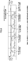
- FIG. 1 It is a figure which shows the apparatus which measures the sticking shift
- positioning with respect to the liquid crystal panel of the optical film sticking position measuring apparatus of this invention The other example of arrangement
- positioning with respect to the liquid crystal panel of the optical film sticking position measuring apparatus of this invention The other example of arrangement
- the optical film sticking position measuring apparatus 101 is an apparatus that is applied to a production line for manufacturing a liquid crystal panel by sticking an optical film to a liquid crystal cell, and inspects the accuracy of sticking the optical film to the liquid crystal cell.
- liquid crystal cell filled with a liquid crystal material between two transparent substrates
- an optical film is attached to one or both sides of the liquid crystal cell. Is called a liquid crystal panel.
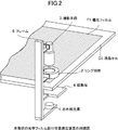
- the optical film sticking position measuring device 101 includes an infrared light source 1 provided on one end side (base) of the L-shaped frame 6 and the other end side (arm portion of the arm portion) of the frame 6.
- the photographing means 3 provided on the end side) and the ring light source 2 provided in the middle of the arm portion of the frame 6 between the infrared light source 1 and the photographing means 3 are provided.
- the imaging means 3 is provided in the optical path of the infrared light source 1 so that the infrared light from the infrared light source 1 can enter.
- the ring light source 2 has substantially the same optical axis as the infrared light source 1, but the light emission direction is the infrared light source. 1 is arranged to be opposite to 1.
- a space through which the liquid crystal panel P1 can pass is opened between the infrared light source 1 and the ring light source 2.
- an example of an L-shaped frame has been given for the frame, but the frame is not limited to this shape. Other shapes may be used as long as the photographing device and the light source can be attached.
- a diffusion plate 4 may be provided between the infrared light source 1 and the ring light source 2 as necessary. In that case, when the sticking position of the polarizing film F1 in the liquid crystal panel P1 is measured, the infrared light from the shell of the infrared light source 1 is projected onto the liquid crystal panel P1 through the diffusion plate 4.
- the photographing means 3 includes a camera 31.
- a lens 32 can be further attached to the camera 31 as necessary.
- the type of the camera 31 is not limited as long as the camera 31 can shoot with infrared rays from the infrared light source 1. Further, the wavelength of infrared rays can be appropriately adjusted as necessary, but is preferably in the range of 780 to 1000 nm.
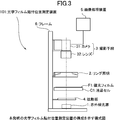
- the optical film sticking position measuring device 101 is installed at a predetermined measuring position in the liquid crystal panel production line.
- the optical film sticking position measuring device 101 is located at the corner of the liquid crystal panel P1 to be measured, and the liquid crystal panel P1 is the infrared light source 1 (or diffuser plate 4) and the ring light source 2. It is arranged to be between.
- the infrared light source 1 When measuring, first, the infrared light source 1 is turned on, the infrared light passes through the liquid crystal panel, and the camera 31 captures an image of the transmitted light. Further, the ring light source 2 is turned on, the light is reflected by the liquid crystal panel, and the camera 31 captures an image of the reflected light.
- a polarizing film is attached to one surface of the liquid crystal cell C1 in the liquid crystal panel P1.
- the liquid crystal cell C1 has a configuration in which a liquid crystal material is filled between the transparent glass substrates in the display region, and a black matrix is provided between the transparent glass substrates outside the display region.
- the black matrix is included in the captured image due to the difference in transmittance between the display area portion, the transparent glass substrate portion, the black matrix BM, and the polarizing film, respectively.
- the edge of the BM and the edge of the polarizing film are clearly copied.
- the light emitted from the ring light source is visible light and is reflected by the surface of the liquid crystal cell or the polarizing film.
- the unevenness on the liquid crystal panel shines by this reflected light, and the edge of the liquid crystal cell C1 and the edge of the polarizing film F1 are clearly copied in the image taken with this reflected light.
- the transmitted light irradiated from the infrared light source 1 and transmitted through the liquid crystal panel P1 passes through the central hole of the ring light source 2 and reaches the camera 31.
- the camera 31 captures an image reflected by the transmitted light, and an image (FIG. 5a) is obtained in which the shape of the black matrix BM in the liquid crystal cell C1 and the shape of the polarizing film F1 attached to the liquid crystal cell C1 are reflected.
- the infrared light source 1 is turned off and the ring light source 2 provided above the liquid crystal panel P1 is turned on, the light from the ring light source 2 reaches the liquid crystal panel P1, is reflected by the liquid crystal panel P1, and It passes through the hole in the center of the light source 2 and reaches the camera 31. And by the action
- An image by transmitted light and an image by reflected light captured by the camera 31 are respectively transmitted to the image processing device 5, and (1) the position of the end of the polarizing film from the end of the black matrix BM as shown in FIG. (2) Two images of the polarizing film sticking position of the polarizing film edge from the outer edge of the liquid crystal cell are obtained.
- the image data is further transmitted to the measuring device, where the polarizing film sticking position is measured. That is, first, as shown in FIG. 5a, the distance L1 between the inner edge of the black matrix and the outer edge of the polarizing film in the liquid crystal cell is measured in the longitudinal direction and the width direction of the liquid crystal panel P1, respectively. Next, as shown in FIG. 5b, the distance L2 between the outer edge of the polarizing film F1 and the outer edge of the liquid crystal cell C1 is also measured in the longitudinal direction and the width direction of the liquid crystal panel P1.
- the measured distance L1 and distance L2 are respectively compared with a predetermined reference distance range, and if it is within the predetermined reference distance range, it is determined that the polarizing film F1 has been attached to a predetermined position. On the other hand, if the distance L1 and the distance L2 are out of the reference distance range, it is determined that the polarizing film F1 is shifted and the liquid crystal panel is defective.
- the infrared light source 1 and the ring light source 2 are used in combination to photograph the corner of the liquid crystal panel twice, and the distance L1 between the end of the black matrix inside the liquid crystal cell and the end of the polarizing film is obtained by transmission imaging with infrared transmission illumination.
- the polarizing film sticking position on the liquid crystal panel is doubled. It is confirmed and the position of the polarizing film can be measured accurately.
- the edge of the black matrix in the liquid crystal cell is used as a measurement reference in the captured image, the influence of variation due to the manufacture of the outer edge of the liquid crystal cell can be suppressed, and the measurement of the position where the polarizing film is applied is performed more accurately.
- the optical film sticking position measuring apparatus 101 of the present invention can be applied to a production line for manufacturing a liquid crystal panel by sticking an optical film on both surfaces of a liquid crystal cell.
- the first optical film is supplied from the first optical film supply device FS1 to the first optical film application device PS1, and applied to one side of the liquid crystal cell that has been conveyed there. Attached.
- the second optical film is supplied from the second optical film supply device FS2 to the second optical film application device PS2, and is then attached to the other surface of the liquid crystal panel on which the first optical film is attached on one side. Attached.
- the liquid crystal panel having the optical films attached on both sides is further conveyed to a downstream process.
- the optical film sticking position measuring device 101 of the present invention is disposed on the downstream side of the first optical film sticking device PS1 and on the downstream side PS2 of the second optical film sticking device.
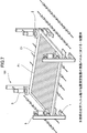
- the optical film sticking position measuring device 101 in order to measure the position of the optical film stuck on one side of the liquid crystal panel P1 by the optical film sticking position measuring device 101, the optical film sticking position measuring device 101, as shown in FIG. are arranged on the same side with respect to the four corners of the liquid crystal panel P1. That is, the optical film sticking position measuring devices 101 located at the four corners of the liquid crystal panel P1 are all in the same direction. Specifically, the camera 31 is located on the same side with respect to the liquid crystal panel P1.
- the optical film sticking position measuring devices 101 With these four optical film sticking position measuring devices 101, the sticking positions of the optical film F1 on the four sides of one side of the liquid crystal panel P1 are measured. In this case, in order to measure the application position of the optical film more accurately, in this embodiment, the optical film application position measuring device 101 is arranged at the four corners of the liquid crystal panel. What is necessary is just to arrange
- Example 3 is different from Example 2 only in that the optical film sticking position measuring device 101 is arranged at only one place on the production line. The description of the same configuration as that of the second embodiment is omitted.
- the optical film sticking position measuring device 101 is disposed only on the downstream side of the second optical film sticking device PS2. That is, in Example 3, after the application of the optical film to both sides of the liquid crystal cell is completed, the attachment positions of the optical films on both sides are measured simultaneously.
- the optical film sticking position measuring device 101 is arranged at the four corners of the liquid crystal panel P1, but the directions of the optical film sticking position measuring devices 101 on the diagonal are the same and adjacent to each other. It arrange
- the optical film sticking position measuring device 101 placed at one pair of diagonals of the liquid crystal panel P1 measures the sticking position of the first optical film, and is placed at the other diagonal of the liquid crystal panel P1.
- the applied position of the second optical film can be measured by the optical film application position measuring device 101 that has been provided.
- optical film application position measuring devices 101 are arranged at the four corners of the liquid crystal panel. What is necessary is just to arrange
- Example 4 although the optical film sticking position measuring apparatus is arrange
- the first optical film sticking position measuring device 101 and the second optical film sticking position measuring device 101 are sequentially arranged downstream of the second optical film sticking device PS2. That is, the two optical film application position measuring devices both perform position inspection on the liquid crystal panel in which the optical film is attached to both surfaces.
- the first optical film sticking position measuring device 101 is arranged in each square of the liquid crystal panel as shown in FIG. 7, and the cameras in the four optical film sticking position measuring devices 101 are all arranged on one side of the liquid crystal panel. Then, the attachment position of the first optical film is measured.
- the second optical film sticking position measuring device 101 is arranged in each square of the liquid crystal panel as shown in FIG. 11, and the cameras in the four optical film sticking position measuring devices 101 are all arranged on the opposite side of the liquid crystal panel. Then, the attachment position of the second optical film is measured.
- both the first optical film and the second optical film can be squarely inspected for the displacement of the application position, and the inspection of the application position is performed with higher accuracy.
- the optical film application position measuring device 101 is arranged at the four corners of the liquid crystal panel in order to measure the optical film application position more accurately. Should be arranged. Even in that case, the camera in the first optical film sticking position measuring device is arranged on one side of the optical display device, and the camera in the second optical film sticking position measuring device is arranged on the opposite side of the optical display device.
- the present invention can be applied to an image display device such as an organic EL display device as a display.
Landscapes
- Physics & Mathematics (AREA)
- General Physics & Mathematics (AREA)
- Nonlinear Science (AREA)
- Chemical & Material Sciences (AREA)
- Crystallography & Structural Chemistry (AREA)
- Optics & Photonics (AREA)
- Liquid Crystal (AREA)
- Length Measuring Devices By Optical Means (AREA)
- Mathematical Physics (AREA)
Applications Claiming Priority (2)
| Application Number | Priority Date | Filing Date | Title |
|---|---|---|---|
| CN201420442537.9 | 2014-08-07 | ||
| CN201420442537.9U CN204128496U (zh) | 2014-08-07 | 2014-08-07 | 光学膜贴合位置测定装置及光学显示装置生产线 |
Publications (1)
| Publication Number | Publication Date |
|---|---|
| WO2016021463A1 true WO2016021463A1 (ja) | 2016-02-11 |
Family
ID=52384845
Family Applications (1)
| Application Number | Title | Priority Date | Filing Date |
|---|---|---|---|
| PCT/JP2015/071515 WO2016021463A1 (ja) | 2014-08-07 | 2015-07-29 | 光学フィルム貼付位置測定装置及び光学表示装置製造ライン |
Country Status (5)
| Country | Link |
|---|---|
| JP (1) | JP5924511B2 (zh) |
| KR (1) | KR101756904B1 (zh) |
| CN (1) | CN204128496U (zh) |
| TW (1) | TWI592715B (zh) |
| WO (1) | WO2016021463A1 (zh) |
Cited By (2)
| Publication number | Priority date | Publication date | Assignee | Title |
|---|---|---|---|---|
| WO2018003578A1 (ja) * | 2016-06-30 | 2018-01-04 | 日本電産サンキョー株式会社 | アライメント装置 |
| CN112596286A (zh) * | 2020-12-15 | 2021-04-02 | 滁州惠科光电科技有限公司 | 一种偏光片检测方法、装置及偏光片贴附机 |
Families Citing this family (6)
| Publication number | Priority date | Publication date | Assignee | Title |
|---|---|---|---|---|
| KR101955757B1 (ko) * | 2016-06-08 | 2019-03-07 | 삼성에스디아이 주식회사 | 필름 처리장치 및 처리방법 |
| TWI745129B (zh) * | 2020-10-20 | 2021-11-01 | 住華科技股份有限公司 | 光學膜偵測系統及應用其之光學膜偵測方法 |
| JP2022090247A (ja) * | 2020-12-07 | 2022-06-17 | 日東電工株式会社 | 光学フィルムの縁部検出方法 |
| JP2022090281A (ja) * | 2020-12-07 | 2022-06-17 | 日東電工株式会社 | 光学フィルムの縁部検出方法 |
| CN114111607B (zh) * | 2021-09-30 | 2024-01-23 | 杭州徐睿机械有限公司 | 一种跳转接头压装组件间隙的检测装置及检测方法 |
| CN114505813B (zh) * | 2022-01-19 | 2023-05-05 | 业成科技(成都)有限公司 | 贴合装置及贴合方法 |
Citations (4)
| Publication number | Priority date | Publication date | Assignee | Title |
|---|---|---|---|---|
| JP2005165097A (ja) * | 2003-12-04 | 2005-06-23 | Yamatake Corp | 偏光板貼り付け位置検査装置 |
| JP2005214962A (ja) * | 2004-01-30 | 2005-08-11 | Samsung Electronics Co Ltd | ディスプレーパネルの検査装置および検査方法 |
| JP2007212939A (ja) * | 2006-02-13 | 2007-08-23 | Hitachi High-Technologies Corp | 位置ずれ検査方法、プログラム及び位置ずれ検査装置 |
| WO2013174112A1 (zh) * | 2012-05-22 | 2013-11-28 | 北京京东方光电科技有限公司 | 偏光板贴附精度检测装置及方法 |
Family Cites Families (3)
| Publication number | Priority date | Publication date | Assignee | Title |
|---|---|---|---|---|
| JP3948522B2 (ja) | 2003-01-30 | 2007-07-25 | 株式会社タカトリ | 液晶パネルの偏光板貼付け精度検査方法 |
| JP2006126483A (ja) | 2004-10-28 | 2006-05-18 | Sharp Corp | 液晶表示パネルの製造方法および液晶表示パネルの製造装置 |
| JP4774123B1 (ja) | 2010-03-18 | 2011-09-14 | 住友化学株式会社 | 偏光板の貼合精度検査方法および貼合精度検査装置 |
-
2014
- 2014-08-07 CN CN201420442537.9U patent/CN204128496U/zh not_active Expired - Lifetime
-
2015
- 2015-01-13 JP JP2015004179A patent/JP5924511B2/ja active Active
- 2015-02-13 TW TW104105056A patent/TWI592715B/zh active
- 2015-03-13 KR KR1020150034962A patent/KR101756904B1/ko active IP Right Grant
- 2015-07-29 WO PCT/JP2015/071515 patent/WO2016021463A1/ja active Application Filing
Patent Citations (4)
| Publication number | Priority date | Publication date | Assignee | Title |
|---|---|---|---|---|
| JP2005165097A (ja) * | 2003-12-04 | 2005-06-23 | Yamatake Corp | 偏光板貼り付け位置検査装置 |
| JP2005214962A (ja) * | 2004-01-30 | 2005-08-11 | Samsung Electronics Co Ltd | ディスプレーパネルの検査装置および検査方法 |
| JP2007212939A (ja) * | 2006-02-13 | 2007-08-23 | Hitachi High-Technologies Corp | 位置ずれ検査方法、プログラム及び位置ずれ検査装置 |
| WO2013174112A1 (zh) * | 2012-05-22 | 2013-11-28 | 北京京东方光电科技有限公司 | 偏光板贴附精度检测装置及方法 |
Cited By (2)
| Publication number | Priority date | Publication date | Assignee | Title |
|---|---|---|---|---|
| WO2018003578A1 (ja) * | 2016-06-30 | 2018-01-04 | 日本電産サンキョー株式会社 | アライメント装置 |
| CN112596286A (zh) * | 2020-12-15 | 2021-04-02 | 滁州惠科光电科技有限公司 | 一种偏光片检测方法、装置及偏光片贴附机 |
Also Published As
| Publication number | Publication date |
|---|---|
| KR101756904B1 (ko) | 2017-07-11 |
| TW201606382A (zh) | 2016-02-16 |
| JP5924511B2 (ja) | 2016-05-25 |
| TWI592715B (zh) | 2017-07-21 |
| KR20160018328A (ko) | 2016-02-17 |
| CN204128496U (zh) | 2015-01-28 |
| JP2016038565A (ja) | 2016-03-22 |
Similar Documents
| Publication | Publication Date | Title |
|---|---|---|
| JP5924511B2 (ja) | 光学フィルム貼付位置測定装置 | |
| TWI542863B (zh) | 光學特性測量方法以及裝置 | |
| KR20110088706A (ko) | 평판 유리 표면 이물질 검사 장치 | |
| TW200806976A (en) | Apparatus for inspecting substrate and method of inspecting substrate using the same | |
| TWI647446B (zh) | 柔性顯示板檢查用夾具及利用其的檢查裝置 | |
| TWI702386B (zh) | 遠心亮場與環形暗場無縫融合式照射 | |
| JP2016038565A5 (zh) | ||
| TW201606290A (zh) | 透明基板之外觀檢查裝置及外觀檢查方法 | |
| KR20150085224A (ko) | 기판의 에지부 검사장치 | |
| JP6004157B2 (ja) | 3次元液晶表示装置の製造装置及び製造方法 | |
| TWI545314B (zh) | Method and method for checking unevenness of film thickness | |
| TW201314384A (zh) | 膜片曝光裝置 | |
| CN107677219A (zh) | 一种平面平行度测量装置及测量方法 | |
| JP5621498B2 (ja) | ムラ欠陥の検査方法 | |
| JP2014095617A (ja) | パターン測定装置およびパターン測定方法 | |
| JP2005241586A (ja) | 光学フィルムの検査装置および光学フィルムの検査方法 | |
| JP5506555B2 (ja) | 異物検査装置、それを用いた露光装置及びデバイスの製造方法 | |
| TWM477571U (zh) | 一種用以擷取一物件影像的擷取裝置以及影像檢測裝置 | |
| TWM451540U (zh) | 檢測裝置 | |
| JP7105925B2 (ja) | ディスプレイユニットの異物検査システム | |
| TWI795552B (zh) | 測量方法以及測量裝置 | |
| KR20140087585A (ko) | 편광 필름 검사 장치 | |
| JP2009174957A (ja) | 異物検出方法および装置 | |
| JP6127458B2 (ja) | パターン測定装置およびパターン測定方法 | |
| TW200804796A (en) | Method of inspecting a pattern defect, substrate, having a test pattern for inspecting a pattern defect, apparatus for inspecting a pattern defect, method of producing a photomask, and method of producing a substrate for a display device |
Legal Events
| Date | Code | Title | Description |
|---|---|---|---|
| 121 | Ep: the epo has been informed by wipo that ep was designated in this application |
Ref document number: 15829984 Country of ref document: EP Kind code of ref document: A1 |
|
| NENP | Non-entry into the national phase |
Ref country code: DE |
|
| NENP | Non-entry into the national phase |
Ref country code: JP |
|
| 122 | Ep: pct application non-entry in european phase |
Ref document number: 15829984 Country of ref document: EP Kind code of ref document: A1 |