WO2016021463A1 - 光学フィルム貼付位置測定装置及び光学表示装置製造ライン - Google Patents
光学フィルム貼付位置測定装置及び光学表示装置製造ライン Download PDFInfo
- Publication number
- WO2016021463A1 WO2016021463A1 PCT/JP2015/071515 JP2015071515W WO2016021463A1 WO 2016021463 A1 WO2016021463 A1 WO 2016021463A1 JP 2015071515 W JP2015071515 W JP 2015071515W WO 2016021463 A1 WO2016021463 A1 WO 2016021463A1
- Authority
- WO
- WIPO (PCT)
- Prior art keywords
- optical film
- optical
- display device
- position measuring
- sticking position
- Prior art date
Links
Images


Classifications
-
- G—PHYSICS
- G01—MEASURING; TESTING
- G01B—MEASURING LENGTH, THICKNESS OR SIMILAR LINEAR DIMENSIONS; MEASURING ANGLES; MEASURING AREAS; MEASURING IRREGULARITIES OF SURFACES OR CONTOURS
- G01B11/00—Measuring arrangements characterised by the use of optical techniques
-
- G—PHYSICS
- G01—MEASURING; TESTING
- G01B—MEASURING LENGTH, THICKNESS OR SIMILAR LINEAR DIMENSIONS; MEASURING ANGLES; MEASURING AREAS; MEASURING IRREGULARITIES OF SURFACES OR CONTOURS
- G01B11/00—Measuring arrangements characterised by the use of optical techniques
- G01B11/14—Measuring arrangements characterised by the use of optical techniques for measuring distance or clearance between spaced objects or spaced apertures
-
- G—PHYSICS
- G02—OPTICS
- G02F—OPTICAL DEVICES OR ARRANGEMENTS FOR THE CONTROL OF LIGHT BY MODIFICATION OF THE OPTICAL PROPERTIES OF THE MEDIA OF THE ELEMENTS INVOLVED THEREIN; NON-LINEAR OPTICS; FREQUENCY-CHANGING OF LIGHT; OPTICAL LOGIC ELEMENTS; OPTICAL ANALOGUE/DIGITAL CONVERTERS
- G02F1/00—Devices or arrangements for the control of the intensity, colour, phase, polarisation or direction of light arriving from an independent light source, e.g. switching, gating or modulating; Non-linear optics
- G02F1/01—Devices or arrangements for the control of the intensity, colour, phase, polarisation or direction of light arriving from an independent light source, e.g. switching, gating or modulating; Non-linear optics for the control of the intensity, phase, polarisation or colour
- G02F1/13—Devices or arrangements for the control of the intensity, colour, phase, polarisation or direction of light arriving from an independent light source, e.g. switching, gating or modulating; Non-linear optics for the control of the intensity, phase, polarisation or colour based on liquid crystals, e.g. single liquid crystal display cells
- G02F1/133—Constructional arrangements; Operation of liquid crystal cells; Circuit arrangements
- G02F1/1333—Constructional arrangements; Manufacturing methods
- G02F1/1335—Structural association of cells with optical devices, e.g. polarisers or reflectors
Definitions
- the present invention relates to an optical film pasting position measuring device.
- the process of manufacturing a display it is necessary to attach an optical film to the optical element in order to realize the display function of the optical display device.
- the accuracy of applying the optical film is closely related to the display quality of the optical display device that is the product.
- Patent Document 1 After attaching a polarizing plate to a liquid crystal panel, as shown in FIG. 1, any one of the four corners of the liquid crystal panel 1 or a plurality of edge portions is perpendicular to the side surface of the liquid crystal panel 1.
- the image is taken by the CCD cameras 28 and 29 from a certain direction, and the distance from the liquid crystal panel 1 end to the end of the polarizing plate 3 in the taken image is measured by image processing to determine whether it is a non-defective product An inspection method is disclosed.
- Patent Document 2 discloses a method of photographing all the four corners of a polarizing plate bonded to a liquid crystal panel with a camera and calculating the amount of misalignment of the polarizing plate using the obtained image data.
- the present invention has been made to solve the above-described problems, and provides an optical film sticking position measuring apparatus that can measure the sticking position of an optical film with high accuracy by taking image data with respect to an optical display device. Providing is a problem to be solved.
- the optical film sticking position measuring device of the present invention measures the sticking position of the optical film with respect to the optical display device in which the optical film is stuck to the optical element, and is provided on the frame and one end side of the frame.
- An infrared light source that emits infrared light
- an imaging unit that is provided on the other end side of the frame and that is configured to receive the infrared ray
- a ring light source that is provided between the infrared light source and the imaging unit.
- the infrared light source and the ring light source are characterized in that the optical axes are substantially coaxial, the light emission directions face each other, and a space through which the optical display device can pass is provided.
- This optical film sticking position measuring device can use an infrared light source and a ring light source together to take an image of an optical display device passing between them, and can accurately measure the position of the optical film.
- the infrared light emitted from the infrared light source is transmitted through the optical display device, and the distance between the edge of the black matrix inside the optical element and the outer edge of the optical film is determined by the transmitted light.
- the light emitted from the ring light source is reflected by the optical display device, and the reflected light may be used to photograph the distance between the outer edge of the optical element and the outer edge of the optical film.
- the position of the optical film can be measured more accurately because the end of the black matrix in the optical element is used as a reference to measure the position of the optical film.
- a diffusion plate may be further provided between the infrared light source and the optical display device. Thereby, the emitted infrared rays are uniformly diffused, and the image quality can be further improved.
- the photographing means is configured to transmit the photographed image data to the image processing apparatus. Therefore, since the image filmed by the transmitted light and the image photographed by the reflected light can be double confirmed by the image processing apparatus, the position of the optical film can be measured more accurately.
- the present invention also provides an optical display device production line for producing an optical display device by attaching an optical film to both surfaces of an optical element.
- the production line sequentially includes a first optical film sticking device for sticking a first optical film on one surface of the optical element, and a second optical film sticking device for sticking a second optical film on the other surface of the optical element.
- An optical film sticking position measuring device is arranged between the first optical film sticking device and the second optical film sticking device, and measures the sticking position of the first optical film to measure the second optical film.
- An optical film sticking position measuring device according to the present invention is arranged downstream of the film sticking apparatus, and measures the sticking position of the second optical film.
- the optical film sticking position measuring device is arranged at least at one corner of the optical display device in any arrangement place. In order to improve measurement accuracy, it is preferable that the optical film sticking position measuring device is arranged at four corners of the optical display device so that the photographing unit is on the same side with respect to the optical display device.
- the optical film sticking position is immediately measured, and if it is determined to be defective, it can be processed immediately, so the yield can be improved.
- the optical film sticking position measuring device is disposed only on the downstream side of the second optical film sticking device, and the sticking positions of the first optical film and the second optical film are determined. It can also be configured to measure simultaneously.
- the optical film sticking position measuring device is disposed at least at two adjacent corners of the optical display device, and the imaging means of the optical film sticking position measuring device disposed adjacent to each other is in a different direction with respect to the optical display device. It is arranged to become.
- the optical film sticking position measuring device is provided at the four corners of the optical display device, and the photographing means in the diagonal optical film sticking position measuring device is the same as the optical display device. It is preferable that the photographing means in the adjacent optical film pasting position measuring device is located on the side of the optical display device and located on a different side.
- the attachment positions of the optical films on both sides can be measured in a lump, which simplifies the apparatus and improves the production rate.
- an optical film sticking position measuring device for measuring the sticking position of the first optical film, and an optical film sticking position for measuring the sticking position of the second optical film.
- Measuring devices are sequentially arranged at two locations, and the optical film sticking position measuring device is the optical film sticking position measuring device of the present invention, and measures the sticking position of the first optical film.
- the photographing means in the optical display device is located on one side with respect to the optical display device, and the photographing means in the optical film sticking position measuring device for measuring the sticking position of the second optical film is located on the opposite side of the optical display device.
- the optical film sticking position measuring device for measuring the sticking position of the first optical film and the optical film sticking position measuring device for measuring the sticking position of the second optical film include the optical display. It is preferable to arrange at the four corners of the device.
- FIG. 1 It is a figure which shows the apparatus which measures the sticking shift
- positioning with respect to the liquid crystal panel of the optical film sticking position measuring apparatus of this invention The other example of arrangement
- positioning with respect to the liquid crystal panel of the optical film sticking position measuring apparatus of this invention The other example of arrangement
- the optical film sticking position measuring apparatus 101 is an apparatus that is applied to a production line for manufacturing a liquid crystal panel by sticking an optical film to a liquid crystal cell, and inspects the accuracy of sticking the optical film to the liquid crystal cell.
- liquid crystal cell filled with a liquid crystal material between two transparent substrates
- an optical film is attached to one or both sides of the liquid crystal cell. Is called a liquid crystal panel.
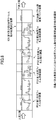
- the optical film sticking position measuring device 101 includes an infrared light source 1 provided on one end side (base) of the L-shaped frame 6 and the other end side (arm portion of the arm portion) of the frame 6.
- the photographing means 3 provided on the end side) and the ring light source 2 provided in the middle of the arm portion of the frame 6 between the infrared light source 1 and the photographing means 3 are provided.
- the imaging means 3 is provided in the optical path of the infrared light source 1 so that the infrared light from the infrared light source 1 can enter.
- the ring light source 2 has substantially the same optical axis as the infrared light source 1, but the light emission direction is the infrared light source. 1 is arranged to be opposite to 1.
- a space through which the liquid crystal panel P1 can pass is opened between the infrared light source 1 and the ring light source 2.
- an example of an L-shaped frame has been given for the frame, but the frame is not limited to this shape. Other shapes may be used as long as the photographing device and the light source can be attached.
- a diffusion plate 4 may be provided between the infrared light source 1 and the ring light source 2 as necessary. In that case, when the sticking position of the polarizing film F1 in the liquid crystal panel P1 is measured, the infrared light from the shell of the infrared light source 1 is projected onto the liquid crystal panel P1 through the diffusion plate 4.
- the photographing means 3 includes a camera 31.
- a lens 32 can be further attached to the camera 31 as necessary.
- the type of the camera 31 is not limited as long as the camera 31 can shoot with infrared rays from the infrared light source 1. Further, the wavelength of infrared rays can be appropriately adjusted as necessary, but is preferably in the range of 780 to 1000 nm.
- the optical film sticking position measuring device 101 is installed at a predetermined measuring position in the liquid crystal panel production line.
- the optical film sticking position measuring device 101 is located at the corner of the liquid crystal panel P1 to be measured, and the liquid crystal panel P1 is the infrared light source 1 (or diffuser plate 4) and the ring light source 2. It is arranged to be between.
- the infrared light source 1 When measuring, first, the infrared light source 1 is turned on, the infrared light passes through the liquid crystal panel, and the camera 31 captures an image of the transmitted light. Further, the ring light source 2 is turned on, the light is reflected by the liquid crystal panel, and the camera 31 captures an image of the reflected light.
- a polarizing film is attached to one surface of the liquid crystal cell C1 in the liquid crystal panel P1.
- the liquid crystal cell C1 has a configuration in which a liquid crystal material is filled between the transparent glass substrates in the display region, and a black matrix is provided between the transparent glass substrates outside the display region.
- the black matrix is included in the captured image due to the difference in transmittance between the display area portion, the transparent glass substrate portion, the black matrix BM, and the polarizing film, respectively.
- the edge of the BM and the edge of the polarizing film are clearly copied.
- the light emitted from the ring light source is visible light and is reflected by the surface of the liquid crystal cell or the polarizing film.
- the unevenness on the liquid crystal panel shines by this reflected light, and the edge of the liquid crystal cell C1 and the edge of the polarizing film F1 are clearly copied in the image taken with this reflected light.
- the transmitted light irradiated from the infrared light source 1 and transmitted through the liquid crystal panel P1 passes through the central hole of the ring light source 2 and reaches the camera 31.
- the camera 31 captures an image reflected by the transmitted light, and an image (FIG. 5a) is obtained in which the shape of the black matrix BM in the liquid crystal cell C1 and the shape of the polarizing film F1 attached to the liquid crystal cell C1 are reflected.
- the infrared light source 1 is turned off and the ring light source 2 provided above the liquid crystal panel P1 is turned on, the light from the ring light source 2 reaches the liquid crystal panel P1, is reflected by the liquid crystal panel P1, and It passes through the hole in the center of the light source 2 and reaches the camera 31. And by the action
- An image by transmitted light and an image by reflected light captured by the camera 31 are respectively transmitted to the image processing device 5, and (1) the position of the end of the polarizing film from the end of the black matrix BM as shown in FIG. (2) Two images of the polarizing film sticking position of the polarizing film edge from the outer edge of the liquid crystal cell are obtained.
- the image data is further transmitted to the measuring device, where the polarizing film sticking position is measured. That is, first, as shown in FIG. 5a, the distance L1 between the inner edge of the black matrix and the outer edge of the polarizing film in the liquid crystal cell is measured in the longitudinal direction and the width direction of the liquid crystal panel P1, respectively. Next, as shown in FIG. 5b, the distance L2 between the outer edge of the polarizing film F1 and the outer edge of the liquid crystal cell C1 is also measured in the longitudinal direction and the width direction of the liquid crystal panel P1.
- the measured distance L1 and distance L2 are respectively compared with a predetermined reference distance range, and if it is within the predetermined reference distance range, it is determined that the polarizing film F1 has been attached to a predetermined position. On the other hand, if the distance L1 and the distance L2 are out of the reference distance range, it is determined that the polarizing film F1 is shifted and the liquid crystal panel is defective.
- the infrared light source 1 and the ring light source 2 are used in combination to photograph the corner of the liquid crystal panel twice, and the distance L1 between the end of the black matrix inside the liquid crystal cell and the end of the polarizing film is obtained by transmission imaging with infrared transmission illumination.
- the polarizing film sticking position on the liquid crystal panel is doubled. It is confirmed and the position of the polarizing film can be measured accurately.
- the edge of the black matrix in the liquid crystal cell is used as a measurement reference in the captured image, the influence of variation due to the manufacture of the outer edge of the liquid crystal cell can be suppressed, and the measurement of the position where the polarizing film is applied is performed more accurately.
- the optical film sticking position measuring apparatus 101 of the present invention can be applied to a production line for manufacturing a liquid crystal panel by sticking an optical film on both surfaces of a liquid crystal cell.
- the first optical film is supplied from the first optical film supply device FS1 to the first optical film application device PS1, and applied to one side of the liquid crystal cell that has been conveyed there. Attached.
- the second optical film is supplied from the second optical film supply device FS2 to the second optical film application device PS2, and is then attached to the other surface of the liquid crystal panel on which the first optical film is attached on one side. Attached.
- the liquid crystal panel having the optical films attached on both sides is further conveyed to a downstream process.
- the optical film sticking position measuring device 101 of the present invention is disposed on the downstream side of the first optical film sticking device PS1 and on the downstream side PS2 of the second optical film sticking device.
- the optical film sticking position measuring device 101 in order to measure the position of the optical film stuck on one side of the liquid crystal panel P1 by the optical film sticking position measuring device 101, the optical film sticking position measuring device 101, as shown in FIG. are arranged on the same side with respect to the four corners of the liquid crystal panel P1. That is, the optical film sticking position measuring devices 101 located at the four corners of the liquid crystal panel P1 are all in the same direction. Specifically, the camera 31 is located on the same side with respect to the liquid crystal panel P1.
- the optical film sticking position measuring devices 101 With these four optical film sticking position measuring devices 101, the sticking positions of the optical film F1 on the four sides of one side of the liquid crystal panel P1 are measured. In this case, in order to measure the application position of the optical film more accurately, in this embodiment, the optical film application position measuring device 101 is arranged at the four corners of the liquid crystal panel. What is necessary is just to arrange
- Example 3 is different from Example 2 only in that the optical film sticking position measuring device 101 is arranged at only one place on the production line. The description of the same configuration as that of the second embodiment is omitted.
- the optical film sticking position measuring device 101 is disposed only on the downstream side of the second optical film sticking device PS2. That is, in Example 3, after the application of the optical film to both sides of the liquid crystal cell is completed, the attachment positions of the optical films on both sides are measured simultaneously.
- the optical film sticking position measuring device 101 is arranged at the four corners of the liquid crystal panel P1, but the directions of the optical film sticking position measuring devices 101 on the diagonal are the same and adjacent to each other. It arrange
- the optical film sticking position measuring device 101 placed at one pair of diagonals of the liquid crystal panel P1 measures the sticking position of the first optical film, and is placed at the other diagonal of the liquid crystal panel P1.
- the applied position of the second optical film can be measured by the optical film application position measuring device 101 that has been provided.
- optical film application position measuring devices 101 are arranged at the four corners of the liquid crystal panel. What is necessary is just to arrange
- Example 4 although the optical film sticking position measuring apparatus is arrange
- the first optical film sticking position measuring device 101 and the second optical film sticking position measuring device 101 are sequentially arranged downstream of the second optical film sticking device PS2. That is, the two optical film application position measuring devices both perform position inspection on the liquid crystal panel in which the optical film is attached to both surfaces.
- the first optical film sticking position measuring device 101 is arranged in each square of the liquid crystal panel as shown in FIG. 7, and the cameras in the four optical film sticking position measuring devices 101 are all arranged on one side of the liquid crystal panel. Then, the attachment position of the first optical film is measured.
- the second optical film sticking position measuring device 101 is arranged in each square of the liquid crystal panel as shown in FIG. 11, and the cameras in the four optical film sticking position measuring devices 101 are all arranged on the opposite side of the liquid crystal panel. Then, the attachment position of the second optical film is measured.
- both the first optical film and the second optical film can be squarely inspected for the displacement of the application position, and the inspection of the application position is performed with higher accuracy.
- the optical film application position measuring device 101 is arranged at the four corners of the liquid crystal panel in order to measure the optical film application position more accurately. Should be arranged. Even in that case, the camera in the first optical film sticking position measuring device is arranged on one side of the optical display device, and the camera in the second optical film sticking position measuring device is arranged on the opposite side of the optical display device.
- the present invention can be applied to an image display device such as an organic EL display device as a display.
Landscapes
- Physics & Mathematics (AREA)
- General Physics & Mathematics (AREA)
- Nonlinear Science (AREA)
- Chemical & Material Sciences (AREA)
- Crystallography & Structural Chemistry (AREA)
- Optics & Photonics (AREA)
- Liquid Crystal (AREA)
- Length Measuring Devices By Optical Means (AREA)
- Mathematical Physics (AREA)
Abstract
光学表示装置に対して画像データを撮ることにより簡単で高精度に光学フィルムの貼付位置を測定できる光学フィルム貼付位置測定装置を提供する。光学素子に光学フィルムが貼り付けられた光学表示装置に対して光学フィルムの貼付位置を測定する光学フィルム貼付位置測定装置であって、フレームと、該フレームの一端側に設けられ、赤外線を出射する赤外線光源と、該フレームの他端側に設けられ、該赤外線が入射するように設けられる撮影手段と、赤外線光源と撮影手段との間に設けられるリング光源と、を備え、該赤外線光源と該リング光源は、光軸がほぼ同軸であって、光の出射方向が対向し、その間を光学表示装置が通過できるように空間が形成されている。この光学フィルム貼付位置測定装置により、赤外線光源とリング光源を併用して光学フィルムの貼付位置を測定し、簡単な構成で高精度な測定が実現できる。
Description
本発明は光学フィルム貼付位置測定装置に関する。
ディスプレイを製造する工程において、光学表示装置の表示機能を実現するため、光学素子に光学フィルムを貼付ける必要がある。この場合、光学フィルムの貼付精度は、製品となった光学表示装置の表示品質に密に関連している。
そして、光学表示装置における光学フィルムの貼付ズレ量を検出する技術は、従来より知られている。例えば、特許文献1には、偏光板を液晶パネルに貼り付けた後に、図1に示すように、液晶パネル1の四隅のいずれか又は複数のエッジ部付近を液晶パネル1側面に対して垂直となる方向からCCDカメラ28,29により撮影し、撮影された画像中の液晶パネル1端部から偏光板3端部までの距離を画像処理により測定し、良品であるか否かを判断する貼付精度検査方法が開示されている。
また、特許文献2には、液晶パネルに貼り合わせた偏光板の四隅のすべてをカメラで撮影し、得られた画像データを用いて偏光板の貼付ズレ量などを算出する方法が開示される。
しかし、特許文献1に開示された偏光板の貼付ズレ量の検出方法では、液晶パネルの側面に対して垂直な方向から液晶パネルの四隅を撮影する。しかし、液晶パネル及び偏光板は、その厚みが小さいため、この測定方法自体の精度が確保し難い。また、特許文献2の方法によれば、CCDカメラを利用して液晶パネルの四隅を撮影するが、液晶パネルと偏光板との境界がはっきりと写らず、高精度な測定ができない問題点がある。
本発明は、上記問題点を解決するためになされたものであり、光学表示装置に対して画像データを撮ることにより簡単で高精度に光学フィルムの貼付位置を測定できる光学フィルム貼付位置測定装置を提供することを解決すべき課題とする。
本発明の光学フィルム貼付位置測定装置は、光学素子に光学フィルムが貼り付けられた光学表示装置に対して光学フィルムの貼付位置を測定するものであり、フレームと、該フレームの一端側に設けられ、赤外線を出射する赤外線光源と、該フレームの他端側に設けられ、前記赤外線が入射するように設けられる撮影手段と、前記赤外線光源と前記撮影手段との間に設けられるリング光源と、を備え、前記赤外線光源と前記リング光源は、光軸がほぼ同軸であって、光の出射方向が対向し、その間に前記光学表示装置が通過できる空間が設けられていることを特徴とする。
この光学フィルム貼付位置測定装置により、赤外線光源とリング光源を併用して、その間に通過する光学表示装置の画像を撮ることができ、光学フィルムの位置が正確に測ることができる。
また、この光学フィルム貼付位置測定装置は、前記赤外線光源から出射した赤外線が前記光学表示装置を透過し、その透過光により光学素子内部におけるブラックマトリクスの端部と前記光学フィルムの外縁との距離を撮影し、前記リング光源から出射した光が前記光学表示装置により反射され、その反射光により、光学素子の外縁と前記光学フィルムの外縁との距離を撮影するように構成してもよい。
これにより、光学素子におけるブラックマトリクスの端部が基準として光学フィルムの位置を測定するため、より正確に光学フィルムの位置を測定することができる。
また、前記赤外線光源と前記光学表示装置の間に拡散板をさらに備えてもよい。これにより、出射された赤外線が均一に拡散され、画像の質が一層向上できるようになる。
また、前記撮影手段は、撮影された画像データを画像処理装置に送信するように構成される。これにより、透過光により撮影した画像と反射光により撮影した画像とが画像処理装置で偏光フィルムの貼付位置が2重に確認できるため、より正確に光学フィルムの貼付位置を測定できる。
本発明は、また光学フィルムを光学素子の両面に貼り付けて光学表示装置を製造する光学表示装置製造ラインを提供する。この製造ラインは、前記光学素子の一面に第1光学フィルムを貼り付ける第1光学フィルム貼付装置と、前記光学素子の他面に第2光学フィルムを貼り付ける第2光学フィルム貼付装置と、を順次備える。前記第1光学フィルム貼付装置と前記第2光学フィルム貼付装置との間に、本発明にかかる光学フィルム貼付位置測定装置が配置され、前記第1光学フィルムの貼付位置を測定し、前記第2光学フィルム貼付装置の下流側に、本発明にかかる光学フィルム貼付位置測定装置が配置され、前記第2光学フィルムの貼付位置を測定する。前記光学フィルム貼付位置測定装置は、いずれの配置箇所において、少なくとも前記光学表示装置の一隅に配置される。
また、測定の正確性を向上するため、前記光学フィルム貼付位置測定装置は、前記撮影手段が前記光学表示装置に対して同一側になるように光学表示装置の四隅に配置されることが好ましい。
また、測定の正確性を向上するため、前記光学フィルム貼付位置測定装置は、前記撮影手段が前記光学表示装置に対して同一側になるように光学表示装置の四隅に配置されることが好ましい。
これにより、光学フィルムの貼付が完成するごとに、その光学フィルムの貼付位置をすぐに測定し、不良であると判断すれば、直ちに処理できるため、歩留まりを向上できる。
また、前記の製造ラインにおいて、前記第2光学フィルム貼付装置の下流側にのみ、本発明にかかる光学フィルム貼付位置測定装置が配置され、前記第1光学フィルムと前記第2光学フィルムの貼付位置を同時に測定するように構成することもできる。前記光学フィルム貼付位置測定装置は、少なくとも前記光学表示装置の隣接する二隅に配置され、隣接に配置される光学フィルム貼付位置測定装置の前記撮像手段は、前記光学表示装置に対して異なる向きになるように配置される。
また、測定の正確性を向上するため、前記光学フィルム貼付位置測定装置は、前記光学表示装置の四隅に設けられ、対角にある光学フィルム貼付位置測定装置における撮影手段が前記光学表示装置の同一側に位置し、隣接する光学フィルム貼付位置測定装置における撮影手段が前記光学表示装置の異なる側に位置するように配置することが好ましい。
また、測定の正確性を向上するため、前記光学フィルム貼付位置測定装置は、前記光学表示装置の四隅に設けられ、対角にある光学フィルム貼付位置測定装置における撮影手段が前記光学表示装置の同一側に位置し、隣接する光学フィルム貼付位置測定装置における撮影手段が前記光学表示装置の異なる側に位置するように配置することが好ましい。
これにより、光学素子の両面に光学フィルムの貼付が完成した後に、両面の光学フィルムの貼付位置を一括に測定することができ、装置が簡素になり、生産率も向上できる。
前記の製造ラインにおいて、前記第2光学フィルム貼付装置の下流側に、第1光学フィルムの貼付位置を測定する光学フィルム貼付位置測定装置と、第2光学フィルムの貼付位置を測定する光学フィルム貼付位置測定装置とが、それぞれ二箇所に順次配置され、前記光学フィルム貼付位置測定装置は、本発明の光学フィルム貼付位置測定装置であり、第1光学フィルムの貼付位置を測定する光学フィルム貼付位置測定装置における撮影手段が前記光学表示装置に対して一側に位置し、前記第2光学フィルムの貼付位置を測定する光学フィルム貼付位置測定装置における撮影手段が前記光学表示装置の反対側に位置するように構成する。
また、測定の正確性を向上するため、第1光学フィルムの貼付位置を測定する光学フィルム貼付位置測定装置と、第2光学フィルムの貼付位置を測定する光学フィルム貼付位置測定装置は、前記光学表示装置の四隅に配置されることが好ましい。
また、測定の正確性を向上するため、第1光学フィルムの貼付位置を測定する光学フィルム貼付位置測定装置と、第2光学フィルムの貼付位置を測定する光学フィルム貼付位置測定装置は、前記光学表示装置の四隅に配置されることが好ましい。
以下、本発明の具体的な実施形態を詳しく説明する。なお、以下の実施形態においては、一例として、液晶セルに光学フィルムを貼付けて液晶パネルを製造する場合について説明する。
本発明にかかる光学フィルム貼付位置測定装置101は、光学フィルムを液晶セルに貼付けて液晶パネルを製造する製造ラインに適用され、光学フィルムを液晶セルに貼りつける精度を検査する装置である。
次に、液晶セルC1の両面にそれぞれ偏光フィルムF1を貼り付ける例として、本発明の光学フィルム貼付位置測定装置101の構成及び動作を説明する。
なお、本発明では、二枚の透明基板の間に液晶材料が充填されてセル化されたものは液晶セルと呼ばれ、この液晶セルの片面または両面に光学フィルムが貼り付けられてなったものは液晶パネルと呼ばれる。
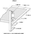
この光学フィルム貼付位置測定装置101は、図2及び図3に示すように、L型フレーム6の一端側(基部)に設けられた赤外線光源1と、該フレーム6の他端側(アーム部の端部側)に設けられた撮影手段3と、赤外線光源1と撮影手段3の間において、このフレーム6のアーム部の途中に設けられたリング光源2とを備える。撮影手段3は、赤外線光源1からの赤外線が入射できるように赤外線光源1の光路に設けられ、リング光源2は、赤外線光源1と光軸がほぼ同一であるが、光の出射方向が赤外線光源1と反対になるように配置される。また、赤外線光源1とリング光源2との間に、液晶パネルP1が通過できる空間が開いている。
ここで、フレームについて、L型フレームの例を挙げたが、フレームは、この形状に限らない。撮影装置及び光源を取り付けることができれば、他の形でもよい。
ここで、フレームについて、L型フレームの例を挙げたが、フレームは、この形状に限らない。撮影装置及び光源を取り付けることができれば、他の形でもよい。
また、必要に応じて、赤外線光源1とリング光源2との間に、拡散板4が設けられても良い。その場合、液晶パネルP1における偏光フィルムF1の貼付位置を測定するとき、赤外線光源1殻の赤外線が拡散板4を通して液晶パネルP1に投射することになる。
また、撮影手段3は、カメラ31により構成される。また、必要に応じて、カメラ31にさらにレンズ32を取り付けることもできる。カメラ31は、赤外線光源1からの赤外線で撮影できるものであれば、その種類は限られない。
また、赤外線の波長は、必要に応じて適宜調整できるが、780~1000nmの範囲内にあることが好ましい。
また、赤外線の波長は、必要に応じて適宜調整できるが、780~1000nmの範囲内にあることが好ましい。
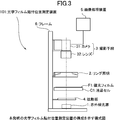
次に、図面を参照しながら、本発明の光学フィルム貼付位置測定装置101の動作を説明する。
この光学フィルム貼付位置測定装置101は、液晶パネルの製造ラインにおける所定の測定位置に設置される。光学フィルム貼付位置測定装置101は、液晶パネルP1が測定位置にあるとき、測定対象となる液晶パネルP1の隅部に位置し、液晶パネルP1が赤外線光源1(または拡散板4)とリング光源2の間にあるように配置される。
測定するとき、まず赤外線光源1を点灯し、その赤外線が液晶パネルを透過して、カメラ31によりその透過光による画像を撮影する。さらに、リング光源2を点灯し、その光が液晶パネルにより反射され、カメラ31によりその反射光による画像を撮影する。
図4に示すように、液晶パネルP1における液晶セルC1の片面には偏光フィルムが貼り付けられる。また、液晶セルC1は、その表示領域の透明ガラス基板の間に液晶材料が充填され、さらにその表示領域の外側の透明ガラス基板の間にブラックマトリクスが設けられた構成である。赤外線光源1からの赤外線が液晶パネルの端部を通過する際に、それぞれ表示領域部、透明ガラス基板部、ブラックマトリクスBM及び偏光フィルムの透過率の差によって、撮られた画像には、ブラックマトリクスBMの縁部と偏光フィルムの縁部がはっきりと写される。また、リング光源から出射した光は可視光であり、液晶セル又は偏光フィルムの表面で反射される。この反射光によって液晶パネル上の凹凸が光り、この反射光で撮られた画像には、液晶セルC1の縁部と偏光フィルムF1の縁部がはっきりと写される。
赤外線光源1から照射され、液晶パネルP1を透過した透過光がリング光源2の中央の孔を通過してカメラ31に到達する。カメラ31はこの透過光で映る画像を撮影し、液晶セルC1におけるブラックマトリクスBMの形と液晶セルC1に貼り付けられた偏光フィルムF1の形が映られた画像(図5a)が得られる。
次に、この赤外線光源1を消灯し、液晶パネルP1の上方に設けられたリング光源2を点灯すると、このリング光源2からの光は液晶パネルP1に到達し、液晶パネルP1により反射され、リング光源2の中央にある孔を通過してカメラ31に到達する。そして、カメラ31の作動により、液晶セルC1と偏光フィルムF1の画像(図5b)が撮像される。
カメラ31により撮像された透過光による画像と反射光による画像がそれぞれ画像処理装置5に送信され、図5aのような(1)ブラックマトリクスBM端部からの偏光フィルム端部の位置と、図5bのような(2)液晶セルの外端からの偏光フィルム端部の位置という偏光フィルムの貼付位置の画像が二つ得られる。
画像データは、さらに測定装置に送信され、そこで偏光フィルムの貼付位置が測定される。即ち、まず、図5aに示すように、液晶パネルP1の縦方向と幅方向について、液晶セル内部におけるブラックマトリクスの内縁と偏光フィルムの外縁との距離L1をそれぞれ測定する。次に、図5bに示すように、同じく液晶パネルP1の縦方向と幅方向について、偏光フィルムF1の外縁と液晶セルC1の外縁との距離L2をそれぞれ測定する。
測定された距離L1と距離L2をそれぞれ所定の基準距離範囲と比較し、所定の基準距離範囲内であれば、偏光フィルムF1が所定の位置に貼り付けられたと判断される。一方、距離L1と距離L2が基準距離範囲から外れれば、偏光フィルムF1がずれた状態にあって液晶パネルが不良品であると判断される。
赤外線光源1とリング光源2とを併用して液晶パネルの隅部を二回撮影し、赤外線透過照明での透過撮像で液晶セル内部のブラックマトリクスの端部と偏光フィルム端部との距離L1と、リング照明での反射撮像で液晶セル端部と偏光フィルム端部との距離L2との二つの測定結果から偏光フィルムの貼付位置を特定するため、液晶パネルにおける偏光フィルムの貼付位置が2重に確認され、正確に偏光フィルムの位置を測定することができる。また、撮像された画像において液晶セルにおけるブラックマトリクスの端部を測定の基準とするため、液晶セルの外縁の製造によるバラつきの影響を抑制でき、偏光フィルムの貼付位置の測定が一層正確に行われる。
本発明の光学フィルム貼付位置測定装置101は、液晶セルの両面に光学フィルムを貼付けて液晶パネルを製造する製造ラインに適用できる。
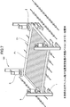
この液晶パネル製造ラインは、図6に示すように、第1光学フィルムが、第1光学フィルム供給装置FS1から第1光学フィルム貼付装置PS1へ供給され、そこで搬送されてきた液晶セルの片面に貼り付けられる。また、第2光学フィルムが、第2光学フィルム供給装置FS2から第2光学フィルム貼付装置PS2へ供給され、そこで搬送されてきた片面に第1光学フィルムが貼り付けられた液晶パネルの他面に貼り付けられる。両面に光学フィルムが貼り付けられた液晶パネルはさらに下流工程に搬送される。
このような生産ラインにおいて、本発明の光学フィルム貼付位置測定装置101が、第1光学フィルム貼付装置PS1の下流側と、第2光学フィルム貼付装置の下流側PS2にそれぞれ配置される。この場合、光学フィルム貼付位置測定装置101により、液晶パネルP1の片面に貼り付けられた光学フィルムの位置を測定するため、光学フィルム貼付位置測定装置101は、図7に示すように、液晶パネルP1に対して同一側であって液晶パネルP1の四隅に配置される。即ち、液晶パネルP1の四隅に位置する光学フィルム貼付位置測定装置101は、すべて同じ向きになっている。具体的に述べると、液晶パネルP1に対して、カメラ31は同じ側に位置する。この四つの光学フィルム貼付位置測定装置101により、液晶パネルP1の片面の4辺における光学フィルムF1の貼付位置を測定する。
この場合、より正確に光学フィルムの貼付位置を測定するため、この実施例には液晶パネルの四隅に光学フィルム貼付位置測定装置101が配置されるが、光学フィルム貼付位置測定装置101は、少なくとも液晶パネルの一隅に配置すればよい。
この場合、より正確に光学フィルムの貼付位置を測定するため、この実施例には液晶パネルの四隅に光学フィルム貼付位置測定装置101が配置されるが、光学フィルム貼付位置測定装置101は、少なくとも液晶パネルの一隅に配置すればよい。
実施例3は、光学フィルム貼付位置測定装置101が製造ラインの1箇所のみに配置される点だけ、実施例2と異なる。実施例2と同じ構成について、その説明を省略する。
実施例3に係る液晶パネル製造ラインにおいては、図8に示すように、光学フィルム貼付位置測定装置101は、第2光学フィルム貼付装置PS2の下流側にのみ配置される。即ち、実施例3において、液晶セルの両面に光学フィルムの貼付が完成した後、両面の光学フィルムの貼付位置を同時に測定する。
その場合、光学フィルム貼付け位置測定装置101は、図9に示すように、液晶パネルP1の四隅に配置されるが、対角にある光学フィルム貼付位置測定装置101の向きが同一であり、隣接する光学フィルム貼付位置測定装置101の向きが逆であるように配置される。具体的に述べると、液晶パネルP1の対角にある光学フィルム貼付位置測定装置101は、カメラ31が液晶パネルP1の同じ側に配置されるが、隣接する光学フィルム貼付位置測定装置101は、カメラ31が液晶パネルP1の異なる側に配置される。
このような配置により、例えば、液晶パネルP1の1対の対角に配置された光学フィルム貼付位置測定装置101により第1光学フィルムの貼付位置を測定し、液晶パネルP1の他の対角に配置された光学フィルム貼付位置測定装置101により第2光学フィルムの貼付位置を測定することができる。
この実施例では、より正確的に光学フィルムの貼付位置を測定するため、液晶パネルの四隅に光学フィルム貼付位置測定装置101が配置されるが、光学フィルム貼付位置測定装置101は、少なくとも液晶パネルの隣接する二隅に配置すればよい。
この実施例では、より正確的に光学フィルムの貼付位置を測定するため、液晶パネルの四隅に光学フィルム貼付位置測定装置101が配置されるが、光学フィルム貼付位置測定装置101は、少なくとも液晶パネルの隣接する二隅に配置すればよい。
実施例4においては、光学フィルム貼付位置測定装置は、液晶パネル製造ラインの二箇所に配置されるが、二つの配置箇所は共に第2光学フィルム貼付位置の下流側に位置する点で、実施例2と異なる。
図10に示すように、第1光学フィルム貼付位置測定装置101と第2光学フィルム貼付位置測定装置101とは、第2光学フィルム貼付け装置PS2の下流に順次配置される。即ち、二つの光学フィルム貼付位置測定装置は、共に両面に光学フィルムが貼り付けた液晶パネルに対して位置検査を行う。
その場合、第1光学フィルム貼付位置測定装置101は、図7のように液晶パネルの四角にそれぞれ配置され、且つ4つの光学フィルム貼付位置測定装置101におけるカメラは、すべて液晶パネルの一側に配置され、第1光学フィルムの貼付け位置を測定する。一方、第2光学フィルム貼付位置測定装置101は、図11のように液晶パネルの四角にそれぞれ配置され、且つ4つの光学フィルム貼付位置測定装置101におけるカメラは、すべて液晶パネルの反対側に配置され、第2光学フィルムの貼付け位置を測定する。
この実施例によれば、第1光学フィルムも第2光学フィルムも四角で貼付位置のズレが検査でき、貼付位置の検査がより高精度に行われる。
この実施例では、より正確的に光学フィルムの貼付位置を測定するため、液晶パネルの四隅に光学フィルム貼付位置測定装置101が配置されるが、光学フィルム貼付位置測定装置101は、少なくとも液晶パネル一隅に配置すればよい。その場合でも、第1光学フィルム貼付位置測定装置におけるカメラは光学表示装置の一側に配置され、第2光学フィルム貼付位置測定装置におけるカメラは、光学表示装置の反対側に配置される。
この実施例では、より正確的に光学フィルムの貼付位置を測定するため、液晶パネルの四隅に光学フィルム貼付位置測定装置101が配置されるが、光学フィルム貼付位置測定装置101は、少なくとも液晶パネル一隅に配置すればよい。その場合でも、第1光学フィルム貼付位置測定装置におけるカメラは光学表示装置の一側に配置され、第2光学フィルム貼付位置測定装置におけるカメラは、光学表示装置の反対側に配置される。
上述したように、図面を参照しながら実施例を挙げて本発明の内容を説明したが、本発明の内容はこれに限らないことが勿論である。請求項の範囲内にあるいろいろな変形や改善がいずれも本発明の範囲内である。例えば、ディスプレイとして、有機EL表示装置等の画像表示装置にも適用することができる。
101 光学フィルム貼付位置測定装置
1 赤外線光源
2 リング光源
3 撮影手段
C1 液晶セル
F1 偏光フィルム
P1 液晶パネル
BM ブラックマトリクス
L1 ブラックマトリクスの端部と偏光フィルムの外縁との距離
L2 液晶セルの外縁と偏光フィルムの外縁との距離
1 赤外線光源
2 リング光源
3 撮影手段
C1 液晶セル
F1 偏光フィルム
P1 液晶パネル
BM ブラックマトリクス
L1 ブラックマトリクスの端部と偏光フィルムの外縁との距離
L2 液晶セルの外縁と偏光フィルムの外縁との距離
Claims (10)
- 光学素子に光学フィルムが貼り付けられた光学表示装置に対して光学フィルムの貼付位置を測定する光学フィルム貼付位置測定装置であって、
フレームと、
前記フレームの一端側に設けられ、赤外線を出射する赤外線光源と、
前記フレームの他端側に設けられ、前記赤外線が入射するように設けられる撮影手段と、
前記赤外線光源と前記撮影手段との間に設けられるリング光源と、
を備え、
前記赤外線光源と前記リング光源は、光軸がほぼ同軸であって、光の出射方向が対向し、その間に前記光学表示装置が通過できるように空間が形成されていることを特徴とする光学フィルム貼付位置測定装置。 - 前記赤外線光源から出射した赤外線が前記光学表示装置を透過し、その透過光により撮影し、光学素子内部におけるブラックマトリクスの端部と前記光学フィルムの外縁との距離を測定し、
前記リング光源から出射した光が前記光学表示装置により反射され、その反射光により撮影し、光学素子の外縁と前記光学フィルムの外縁との距離を測定することを特徴とする請求項1に記載の光学フィルム貼付位置測定装置。 - 前記赤外線光源と前記光学表示装置の間に拡散板をさらに備えることを特徴とする請求項1または2に記載の光学フィルム貼付位置測定装置。
- 前記撮影手段は、撮影された画像データを画像処理装置に送信することを特徴する請求項1また2に記載の光学フィルム貼付位置測定装置。
- 光学フィルムを光学素子の両面に貼り付けて光学表示装置を製造する光学表示装置製造ラインにおいて、
前記光学素子の一面に第1光学フィルムを貼り付ける第1光学フィルム貼付装置と、
前記光学素子の他面に第2光学フィルムを貼り付ける第2光学フィルム貼付装置と、を順次備え、
前記第1光学フィルム貼付装置と前記第2光学フィルム貼付装置との間に、請求項1~4のいずれかに記載の光学フィルム貼付位置測定装置が配置され、前記第1光学フィルムの貼付位置を測定し、
前記第2光学フィルム貼付装置の下流側に、請求項1~4のいずれかに記載の光学フィルム貼付位置測定装置が配置され、前記第2光学フィルムの貼付位置を測定し、
前記光学フィルム貼付位置測定装置は、いずれの配置箇所において、少なくとも前記光学表示装置の一隅に配置されることを特徴とする光学表示装置製造ライン。 - 前記光学フィルム貼付位置測定装置は、前記撮影手段が前記光学表示装置に対して同一側になるように光学表示装置の四隅に配置されることを特徴とする請求項5に記載の光学表示装置製造ライン。
- 光学フィルムを光学素子の両面に貼り付けて光学表示装置を製造する光学表示装置製造ラインにおいて、
前記光学素子の一面に第1光学フィルムを貼り付ける第1光学フィルム貼付装置と、
前記光学素子の他面に第2光学フィルムを貼り付ける第2光学フィルム貼付装置と、を順次備え、
前記第2光学フィルム貼付装置の下流側にのみ、請求項1~4のいずれかに記載の光学フィルム貼付位置測定装置が配置され、前記第1光学フィルムと前記第2光学フィルムの貼付位置を同時に測定し、
前記光学フィルム貼付位置測定装置は、少なくとも前記光学表示装置の隣接する二隅に配置され、隣接に配置される光学フィルム貼付位置測定装置の前記撮像手段は、前記光学表示装置に対して異なる向きになるように配置されることを特徴とする光学表示装置製造ライン。 - 前記光学フィルム貼付位置測定装置は、前記光学表示装置の四隅に設けられ、対角にある光学フィルム貼付位置測定装置における撮影手段が前記光学表示装置に対して同一側に位置し、隣接する光学フィルム貼付位置測定装置における撮影手段が前記光学表示装置に対して異なる側に位置するように配置することを特徴とする請求項7に記載の光学表示装置製造ライン。
- 光学フィルムを光学素子の両面に貼り付けて光学表示装置を製造する光学表示装置製造ラインにおいて、
前記光学素子の一面に第1光学フィルムを貼り付ける第1光学フィルム貼付装置と、
前記光学素子の他面に第2光学フィルムを貼り付ける第2光学フィルム貼付装置と、を順次備え、
前記第2光学フィルム貼付装置の下流側に、第1光学フィルムの貼付位置を測定する光学フィルム貼付位置測定装置と、第2光学フィルムの貼付位置を測定する光学フィルム貼付位置測定装置とが、それぞれ二箇所に順次配置され、
前記光学フィルム貼付位置測定装置は、請求項1~4のいずれかに記載の光学フィルム貼付位置測定装置であり、第1光学フィルムの貼付位置を測定する光学フィルム貼付位置測定装置における撮影手段が前記光学表示装置に対して一側に位置し、前記第2光学フィルムの貼付位置を測定する光学フィルム貼付位置測定装置における撮影手段が前記光学表示装置に対して前記一側の反対側に位置することを特徴とする光学表示装置製造ライン。 - 第1光学フィルムの貼付位置を測定する前記光学フィルム貼付位置測定装置と、第2光学フィルムの貼付位置を測定する前記光学フィルム貼付位置測定装置は、それぞれ前記光学表示装置の四隅に配置されることを特徴とする請求項9に記載の光学表示装置製造ライン。
Applications Claiming Priority (2)
| Application Number | Priority Date | Filing Date | Title |
|---|---|---|---|
| CN201420442537.9 | 2014-08-07 | ||
| CN201420442537.9U CN204128496U (zh) | 2014-08-07 | 2014-08-07 | 光学膜贴合位置测定装置及光学显示装置生产线 |
Publications (1)
| Publication Number | Publication Date |
|---|---|
| WO2016021463A1 true WO2016021463A1 (ja) | 2016-02-11 |
Family
ID=52384845
Family Applications (1)
| Application Number | Title | Priority Date | Filing Date |
|---|---|---|---|
| PCT/JP2015/071515 WO2016021463A1 (ja) | 2014-08-07 | 2015-07-29 | 光学フィルム貼付位置測定装置及び光学表示装置製造ライン |
Country Status (5)
| Country | Link |
|---|---|
| JP (1) | JP5924511B2 (ja) |
| KR (1) | KR101756904B1 (ja) |
| CN (1) | CN204128496U (ja) |
| TW (1) | TWI592715B (ja) |
| WO (1) | WO2016021463A1 (ja) |
Cited By (2)
| Publication number | Priority date | Publication date | Assignee | Title |
|---|---|---|---|---|
| WO2018003578A1 (ja) * | 2016-06-30 | 2018-01-04 | 日本電産サンキョー株式会社 | アライメント装置 |
| CN112596286A (zh) * | 2020-12-15 | 2021-04-02 | 滁州惠科光电科技有限公司 | 一种偏光片检测方法、装置及偏光片贴附机 |
Families Citing this family (6)
| Publication number | Priority date | Publication date | Assignee | Title |
|---|---|---|---|---|
| KR101955757B1 (ko) * | 2016-06-08 | 2019-03-07 | 삼성에스디아이 주식회사 | 필름 처리장치 및 처리방법 |
| TWI745129B (zh) * | 2020-10-20 | 2021-11-01 | 住華科技股份有限公司 | 光學膜偵測系統及應用其之光學膜偵測方法 |
| JP2022090247A (ja) * | 2020-12-07 | 2022-06-17 | 日東電工株式会社 | 光学フィルムの縁部検出方法 |
| JP2022090281A (ja) * | 2020-12-07 | 2022-06-17 | 日東電工株式会社 | 光学フィルムの縁部検出方法 |
| CN114111607B (zh) * | 2021-09-30 | 2024-01-23 | 杭州徐睿机械有限公司 | 一种跳转接头压装组件间隙的检测装置及检测方法 |
| CN114505813B (zh) * | 2022-01-19 | 2023-05-05 | 业成科技(成都)有限公司 | 贴合装置及贴合方法 |
Citations (4)
| Publication number | Priority date | Publication date | Assignee | Title |
|---|---|---|---|---|
| JP2005165097A (ja) * | 2003-12-04 | 2005-06-23 | Yamatake Corp | 偏光板貼り付け位置検査装置 |
| JP2005214962A (ja) * | 2004-01-30 | 2005-08-11 | Samsung Electronics Co Ltd | ディスプレーパネルの検査装置および検査方法 |
| JP2007212939A (ja) * | 2006-02-13 | 2007-08-23 | Hitachi High-Technologies Corp | 位置ずれ検査方法、プログラム及び位置ずれ検査装置 |
| WO2013174112A1 (zh) * | 2012-05-22 | 2013-11-28 | 北京京东方光电科技有限公司 | 偏光板贴附精度检测装置及方法 |
Family Cites Families (3)
| Publication number | Priority date | Publication date | Assignee | Title |
|---|---|---|---|---|
| JP3948522B2 (ja) | 2003-01-30 | 2007-07-25 | 株式会社タカトリ | 液晶パネルの偏光板貼付け精度検査方法 |
| JP2006126483A (ja) | 2004-10-28 | 2006-05-18 | Sharp Corp | 液晶表示パネルの製造方法および液晶表示パネルの製造装置 |
| JP4774123B1 (ja) | 2010-03-18 | 2011-09-14 | 住友化学株式会社 | 偏光板の貼合精度検査方法および貼合精度検査装置 |
-
2014
- 2014-08-07 CN CN201420442537.9U patent/CN204128496U/zh not_active Expired - Lifetime
-
2015
- 2015-01-13 JP JP2015004179A patent/JP5924511B2/ja active Active
- 2015-02-13 TW TW104105056A patent/TWI592715B/zh active
- 2015-03-13 KR KR1020150034962A patent/KR101756904B1/ko active IP Right Grant
- 2015-07-29 WO PCT/JP2015/071515 patent/WO2016021463A1/ja active Application Filing
Patent Citations (4)
| Publication number | Priority date | Publication date | Assignee | Title |
|---|---|---|---|---|
| JP2005165097A (ja) * | 2003-12-04 | 2005-06-23 | Yamatake Corp | 偏光板貼り付け位置検査装置 |
| JP2005214962A (ja) * | 2004-01-30 | 2005-08-11 | Samsung Electronics Co Ltd | ディスプレーパネルの検査装置および検査方法 |
| JP2007212939A (ja) * | 2006-02-13 | 2007-08-23 | Hitachi High-Technologies Corp | 位置ずれ検査方法、プログラム及び位置ずれ検査装置 |
| WO2013174112A1 (zh) * | 2012-05-22 | 2013-11-28 | 北京京东方光电科技有限公司 | 偏光板贴附精度检测装置及方法 |
Cited By (2)
| Publication number | Priority date | Publication date | Assignee | Title |
|---|---|---|---|---|
| WO2018003578A1 (ja) * | 2016-06-30 | 2018-01-04 | 日本電産サンキョー株式会社 | アライメント装置 |
| CN112596286A (zh) * | 2020-12-15 | 2021-04-02 | 滁州惠科光电科技有限公司 | 一种偏光片检测方法、装置及偏光片贴附机 |
Also Published As
| Publication number | Publication date |
|---|---|
| KR101756904B1 (ko) | 2017-07-11 |
| TW201606382A (zh) | 2016-02-16 |
| JP5924511B2 (ja) | 2016-05-25 |
| TWI592715B (zh) | 2017-07-21 |
| KR20160018328A (ko) | 2016-02-17 |
| CN204128496U (zh) | 2015-01-28 |
| JP2016038565A (ja) | 2016-03-22 |
Similar Documents
| Publication | Publication Date | Title |
|---|---|---|
| JP5924511B2 (ja) | 光学フィルム貼付位置測定装置 | |
| TWI542863B (zh) | 光學特性測量方法以及裝置 | |
| KR20110088706A (ko) | 평판 유리 표면 이물질 검사 장치 | |
| TW200806976A (en) | Apparatus for inspecting substrate and method of inspecting substrate using the same | |
| TWI647446B (zh) | 柔性顯示板檢查用夾具及利用其的檢查裝置 | |
| TWI702386B (zh) | 遠心亮場與環形暗場無縫融合式照射 | |
| JP2016038565A5 (ja) | ||
| TW201606290A (zh) | 透明基板之外觀檢查裝置及外觀檢查方法 | |
| KR20150085224A (ko) | 기판의 에지부 검사장치 | |
| JP6004157B2 (ja) | 3次元液晶表示装置の製造装置及び製造方法 | |
| TWI545314B (zh) | Method and method for checking unevenness of film thickness | |
| TW201314384A (zh) | 膜片曝光裝置 | |
| CN107677219A (zh) | 一种平面平行度测量装置及测量方法 | |
| JP5621498B2 (ja) | ムラ欠陥の検査方法 | |
| JP2014095617A (ja) | パターン測定装置およびパターン測定方法 | |
| JP2005241586A (ja) | 光学フィルムの検査装置および光学フィルムの検査方法 | |
| JP5506555B2 (ja) | 異物検査装置、それを用いた露光装置及びデバイスの製造方法 | |
| TWM477571U (zh) | 一種用以擷取一物件影像的擷取裝置以及影像檢測裝置 | |
| TWM451540U (zh) | 檢測裝置 | |
| JP7105925B2 (ja) | ディスプレイユニットの異物検査システム | |
| TWI795552B (zh) | 測量方法以及測量裝置 | |
| KR20140087585A (ko) | 편광 필름 검사 장치 | |
| JP2009174957A (ja) | 異物検出方法および装置 | |
| JP6127458B2 (ja) | パターン測定装置およびパターン測定方法 | |
| TW200804796A (en) | Method of inspecting a pattern defect, substrate, having a test pattern for inspecting a pattern defect, apparatus for inspecting a pattern defect, method of producing a photomask, and method of producing a substrate for a display device |
Legal Events
| Date | Code | Title | Description |
|---|---|---|---|
| 121 | Ep: the epo has been informed by wipo that ep was designated in this application |
Ref document number: 15829984 Country of ref document: EP Kind code of ref document: A1 |
|
| NENP | Non-entry into the national phase |
Ref country code: DE |
|
| NENP | Non-entry into the national phase |
Ref country code: JP |
|
| 122 | Ep: pct application non-entry in european phase |
Ref document number: 15829984 Country of ref document: EP Kind code of ref document: A1 |