WO2016021299A1 - 半導体装置及び半導体装置の製造方法 - Google Patents
半導体装置及び半導体装置の製造方法 Download PDFInfo
- Publication number
- WO2016021299A1 WO2016021299A1 PCT/JP2015/066523 JP2015066523W WO2016021299A1 WO 2016021299 A1 WO2016021299 A1 WO 2016021299A1 JP 2015066523 W JP2015066523 W JP 2015066523W WO 2016021299 A1 WO2016021299 A1 WO 2016021299A1
- Authority
- WO
- WIPO (PCT)
- Prior art keywords
- insulating film
- semiconductor
- contact
- semiconductor substrate
- region
- Prior art date
Links
- 239000004065 semiconductor Substances 0.000 title claims abstract description 194
- 238000004519 manufacturing process Methods 0.000 title claims description 16
- 238000000034 method Methods 0.000 title claims description 7
- 239000010410 layer Substances 0.000 claims abstract description 142
- 239000000758 substrate Substances 0.000 claims abstract description 85
- 239000004020 conductor Substances 0.000 claims abstract description 69
- 239000011229 interlayer Substances 0.000 claims abstract description 50
- 238000005530 etching Methods 0.000 claims description 7
- 229910052782 aluminium Inorganic materials 0.000 claims description 5
- 229910052721 tungsten Inorganic materials 0.000 claims description 5
- 238000007747 plating Methods 0.000 claims description 4
- 238000004544 sputter deposition Methods 0.000 claims description 4
- 229910052802 copper Inorganic materials 0.000 claims description 3
- 239000000463 material Substances 0.000 claims description 3
- 229910052751 metal Inorganic materials 0.000 claims description 2
- 239000002184 metal Substances 0.000 claims description 2
- 238000009413 insulation Methods 0.000 abstract description 4
- 210000000746 body region Anatomy 0.000 description 15
- 239000012535 impurity Substances 0.000 description 9
- 238000011084 recovery Methods 0.000 description 5
- 238000005516 engineering process Methods 0.000 description 3
- XAGFODPZIPBFFR-UHFFFAOYSA-N aluminium Chemical compound [Al] XAGFODPZIPBFFR-UHFFFAOYSA-N 0.000 description 2
- 230000015572 biosynthetic process Effects 0.000 description 2
- WFKWXMTUELFFGS-UHFFFAOYSA-N tungsten Chemical compound [W] WFKWXMTUELFFGS-UHFFFAOYSA-N 0.000 description 2
- 239000010937 tungsten Substances 0.000 description 2
- XUIMIQQOPSSXEZ-UHFFFAOYSA-N Silicon Chemical compound [Si] XUIMIQQOPSSXEZ-UHFFFAOYSA-N 0.000 description 1
- 229910045601 alloy Inorganic materials 0.000 description 1
- 239000000956 alloy Substances 0.000 description 1
- 230000015556 catabolic process Effects 0.000 description 1
- 239000012141 concentrate Substances 0.000 description 1
- 230000005684 electric field Effects 0.000 description 1
- 239000012212 insulator Substances 0.000 description 1
- 238000012986 modification Methods 0.000 description 1
- 230000004048 modification Effects 0.000 description 1
- 230000002250 progressing effect Effects 0.000 description 1
- 229910052710 silicon Inorganic materials 0.000 description 1
- 239000010703 silicon Substances 0.000 description 1
- 229910000679 solder Inorganic materials 0.000 description 1
Images

Classifications
-
- H—ELECTRICITY
- H01—ELECTRIC ELEMENTS
- H01L—SEMICONDUCTOR DEVICES NOT COVERED BY CLASS H10
- H01L27/00—Devices consisting of a plurality of semiconductor or other solid-state components formed in or on a common substrate
- H01L27/02—Devices consisting of a plurality of semiconductor or other solid-state components formed in or on a common substrate including semiconductor components specially adapted for rectifying, oscillating, amplifying or switching and having potential barriers; including integrated passive circuit elements having potential barriers
- H01L27/04—Devices consisting of a plurality of semiconductor or other solid-state components formed in or on a common substrate including semiconductor components specially adapted for rectifying, oscillating, amplifying or switching and having potential barriers; including integrated passive circuit elements having potential barriers the substrate being a semiconductor body
- H01L27/06—Devices consisting of a plurality of semiconductor or other solid-state components formed in or on a common substrate including semiconductor components specially adapted for rectifying, oscillating, amplifying or switching and having potential barriers; including integrated passive circuit elements having potential barriers the substrate being a semiconductor body including a plurality of individual components in a non-repetitive configuration
- H01L27/07—Devices consisting of a plurality of semiconductor or other solid-state components formed in or on a common substrate including semiconductor components specially adapted for rectifying, oscillating, amplifying or switching and having potential barriers; including integrated passive circuit elements having potential barriers the substrate being a semiconductor body including a plurality of individual components in a non-repetitive configuration the components having an active region in common
- H01L27/0705—Devices consisting of a plurality of semiconductor or other solid-state components formed in or on a common substrate including semiconductor components specially adapted for rectifying, oscillating, amplifying or switching and having potential barriers; including integrated passive circuit elements having potential barriers the substrate being a semiconductor body including a plurality of individual components in a non-repetitive configuration the components having an active region in common comprising components of the field effect type
- H01L27/0711—Devices consisting of a plurality of semiconductor or other solid-state components formed in or on a common substrate including semiconductor components specially adapted for rectifying, oscillating, amplifying or switching and having potential barriers; including integrated passive circuit elements having potential barriers the substrate being a semiconductor body including a plurality of individual components in a non-repetitive configuration the components having an active region in common comprising components of the field effect type in combination with bipolar transistors and diodes, or capacitors, or resistors
- H01L27/0716—Devices consisting of a plurality of semiconductor or other solid-state components formed in or on a common substrate including semiconductor components specially adapted for rectifying, oscillating, amplifying or switching and having potential barriers; including integrated passive circuit elements having potential barriers the substrate being a semiconductor body including a plurality of individual components in a non-repetitive configuration the components having an active region in common comprising components of the field effect type in combination with bipolar transistors and diodes, or capacitors, or resistors in combination with vertical bipolar transistors and diodes, or capacitors, or resistors
-
- H—ELECTRICITY
- H01—ELECTRIC ELEMENTS
- H01L—SEMICONDUCTOR DEVICES NOT COVERED BY CLASS H10
- H01L27/00—Devices consisting of a plurality of semiconductor or other solid-state components formed in or on a common substrate
- H01L27/02—Devices consisting of a plurality of semiconductor or other solid-state components formed in or on a common substrate including semiconductor components specially adapted for rectifying, oscillating, amplifying or switching and having potential barriers; including integrated passive circuit elements having potential barriers
- H01L27/04—Devices consisting of a plurality of semiconductor or other solid-state components formed in or on a common substrate including semiconductor components specially adapted for rectifying, oscillating, amplifying or switching and having potential barriers; including integrated passive circuit elements having potential barriers the substrate being a semiconductor body
- H01L27/06—Devices consisting of a plurality of semiconductor or other solid-state components formed in or on a common substrate including semiconductor components specially adapted for rectifying, oscillating, amplifying or switching and having potential barriers; including integrated passive circuit elements having potential barriers the substrate being a semiconductor body including a plurality of individual components in a non-repetitive configuration
- H01L27/07—Devices consisting of a plurality of semiconductor or other solid-state components formed in or on a common substrate including semiconductor components specially adapted for rectifying, oscillating, amplifying or switching and having potential barriers; including integrated passive circuit elements having potential barriers the substrate being a semiconductor body including a plurality of individual components in a non-repetitive configuration the components having an active region in common
- H01L27/0705—Devices consisting of a plurality of semiconductor or other solid-state components formed in or on a common substrate including semiconductor components specially adapted for rectifying, oscillating, amplifying or switching and having potential barriers; including integrated passive circuit elements having potential barriers the substrate being a semiconductor body including a plurality of individual components in a non-repetitive configuration the components having an active region in common comprising components of the field effect type
- H01L27/0727—Devices consisting of a plurality of semiconductor or other solid-state components formed in or on a common substrate including semiconductor components specially adapted for rectifying, oscillating, amplifying or switching and having potential barriers; including integrated passive circuit elements having potential barriers the substrate being a semiconductor body including a plurality of individual components in a non-repetitive configuration the components having an active region in common comprising components of the field effect type in combination with diodes, or capacitors or resistors
-
- H—ELECTRICITY
- H01—ELECTRIC ELEMENTS
- H01L—SEMICONDUCTOR DEVICES NOT COVERED BY CLASS H10
- H01L21/00—Processes or apparatus adapted for the manufacture or treatment of semiconductor or solid state devices or of parts thereof
- H01L21/70—Manufacture or treatment of devices consisting of a plurality of solid state components formed in or on a common substrate or of parts thereof; Manufacture of integrated circuit devices or of parts thereof
- H01L21/71—Manufacture of specific parts of devices defined in group H01L21/70
- H01L21/768—Applying interconnections to be used for carrying current between separate components within a device comprising conductors and dielectrics
-
- H—ELECTRICITY
- H01—ELECTRIC ELEMENTS
- H01L—SEMICONDUCTOR DEVICES NOT COVERED BY CLASS H10
- H01L21/00—Processes or apparatus adapted for the manufacture or treatment of semiconductor or solid state devices or of parts thereof
- H01L21/70—Manufacture or treatment of devices consisting of a plurality of solid state components formed in or on a common substrate or of parts thereof; Manufacture of integrated circuit devices or of parts thereof
- H01L21/77—Manufacture or treatment of devices consisting of a plurality of solid state components or integrated circuits formed in, or on, a common substrate
- H01L21/78—Manufacture or treatment of devices consisting of a plurality of solid state components or integrated circuits formed in, or on, a common substrate with subsequent division of the substrate into plural individual devices
- H01L21/82—Manufacture or treatment of devices consisting of a plurality of solid state components or integrated circuits formed in, or on, a common substrate with subsequent division of the substrate into plural individual devices to produce devices, e.g. integrated circuits, each consisting of a plurality of components
- H01L21/822—Manufacture or treatment of devices consisting of a plurality of solid state components or integrated circuits formed in, or on, a common substrate with subsequent division of the substrate into plural individual devices to produce devices, e.g. integrated circuits, each consisting of a plurality of components the substrate being a semiconductor, using silicon technology
- H01L21/8248—Combination of bipolar and field-effect technology
- H01L21/8249—Bipolar and MOS technology
-
- H—ELECTRICITY
- H01—ELECTRIC ELEMENTS
- H01L—SEMICONDUCTOR DEVICES NOT COVERED BY CLASS H10
- H01L23/00—Details of semiconductor or other solid state devices
- H01L23/52—Arrangements for conducting electric current within the device in operation from one component to another, i.e. interconnections, e.g. wires, lead frames
- H01L23/522—Arrangements for conducting electric current within the device in operation from one component to another, i.e. interconnections, e.g. wires, lead frames including external interconnections consisting of a multilayer structure of conductive and insulating layers inseparably formed on the semiconductor body
- H01L23/5226—Via connections in a multilevel interconnection structure
-
- H—ELECTRICITY
- H01—ELECTRIC ELEMENTS
- H01L—SEMICONDUCTOR DEVICES NOT COVERED BY CLASS H10
- H01L23/00—Details of semiconductor or other solid state devices
- H01L23/52—Arrangements for conducting electric current within the device in operation from one component to another, i.e. interconnections, e.g. wires, lead frames
- H01L23/522—Arrangements for conducting electric current within the device in operation from one component to another, i.e. interconnections, e.g. wires, lead frames including external interconnections consisting of a multilayer structure of conductive and insulating layers inseparably formed on the semiconductor body
- H01L23/528—Geometry or layout of the interconnection structure
- H01L23/5283—Cross-sectional geometry
-
- H—ELECTRICITY
- H01—ELECTRIC ELEMENTS
- H01L—SEMICONDUCTOR DEVICES NOT COVERED BY CLASS H10
- H01L29/00—Semiconductor devices specially adapted for rectifying, amplifying, oscillating or switching and having potential barriers; Capacitors or resistors having potential barriers, e.g. a PN-junction depletion layer or carrier concentration layer; Details of semiconductor bodies or of electrodes thereof ; Multistep manufacturing processes therefor
- H01L29/02—Semiconductor bodies ; Multistep manufacturing processes therefor
- H01L29/06—Semiconductor bodies ; Multistep manufacturing processes therefor characterised by their shape; characterised by the shapes, relative sizes, or dispositions of the semiconductor regions ; characterised by the concentration or distribution of impurities within semiconductor regions
- H01L29/0684—Semiconductor bodies ; Multistep manufacturing processes therefor characterised by their shape; characterised by the shapes, relative sizes, or dispositions of the semiconductor regions ; characterised by the concentration or distribution of impurities within semiconductor regions characterised by the shape, relative sizes or dispositions of the semiconductor regions or junctions between the regions
- H01L29/0692—Surface layout
- H01L29/0696—Surface layout of cellular field-effect devices, e.g. multicellular DMOS transistors or IGBTs
-
- H—ELECTRICITY
- H01—ELECTRIC ELEMENTS
- H01L—SEMICONDUCTOR DEVICES NOT COVERED BY CLASS H10
- H01L29/00—Semiconductor devices specially adapted for rectifying, amplifying, oscillating or switching and having potential barriers; Capacitors or resistors having potential barriers, e.g. a PN-junction depletion layer or carrier concentration layer; Details of semiconductor bodies or of electrodes thereof ; Multistep manufacturing processes therefor
- H01L29/40—Electrodes ; Multistep manufacturing processes therefor
- H01L29/41—Electrodes ; Multistep manufacturing processes therefor characterised by their shape, relative sizes or dispositions
- H01L29/417—Electrodes ; Multistep manufacturing processes therefor characterised by their shape, relative sizes or dispositions carrying the current to be rectified, amplified or switched
- H01L29/41708—Emitter or collector electrodes for bipolar transistors
-
- H—ELECTRICITY
- H01—ELECTRIC ELEMENTS
- H01L—SEMICONDUCTOR DEVICES NOT COVERED BY CLASS H10
- H01L29/00—Semiconductor devices specially adapted for rectifying, amplifying, oscillating or switching and having potential barriers; Capacitors or resistors having potential barriers, e.g. a PN-junction depletion layer or carrier concentration layer; Details of semiconductor bodies or of electrodes thereof ; Multistep manufacturing processes therefor
- H01L29/66—Types of semiconductor device ; Multistep manufacturing processes therefor
- H01L29/66007—Multistep manufacturing processes
- H01L29/66075—Multistep manufacturing processes of devices having semiconductor bodies comprising group 14 or group 13/15 materials
- H01L29/66227—Multistep manufacturing processes of devices having semiconductor bodies comprising group 14 or group 13/15 materials the devices being controllable only by the electric current supplied or the electric potential applied, to an electrode which does not carry the current to be rectified, amplified or switched, e.g. three-terminal devices
- H01L29/66409—Unipolar field-effect transistors
- H01L29/66477—Unipolar field-effect transistors with an insulated gate, i.e. MISFET
- H01L29/66674—DMOS transistors, i.e. MISFETs with a channel accommodating body or base region adjoining a drain drift region
- H01L29/66712—Vertical DMOS transistors, i.e. VDMOS transistors
- H01L29/66734—Vertical DMOS transistors, i.e. VDMOS transistors with a step of recessing the gate electrode, e.g. to form a trench gate electrode
-
- H—ELECTRICITY
- H01—ELECTRIC ELEMENTS
- H01L—SEMICONDUCTOR DEVICES NOT COVERED BY CLASS H10
- H01L29/00—Semiconductor devices specially adapted for rectifying, amplifying, oscillating or switching and having potential barriers; Capacitors or resistors having potential barriers, e.g. a PN-junction depletion layer or carrier concentration layer; Details of semiconductor bodies or of electrodes thereof ; Multistep manufacturing processes therefor
- H01L29/66—Types of semiconductor device ; Multistep manufacturing processes therefor
- H01L29/68—Types of semiconductor device ; Multistep manufacturing processes therefor controllable by only the electric current supplied, or only the electric potential applied, to an electrode which does not carry the current to be rectified, amplified or switched
- H01L29/70—Bipolar devices
- H01L29/72—Transistor-type devices, i.e. able to continuously respond to applied control signals
- H01L29/739—Transistor-type devices, i.e. able to continuously respond to applied control signals controlled by field-effect, e.g. bipolar static induction transistors [BSIT]
- H01L29/7393—Insulated gate bipolar mode transistors, i.e. IGBT; IGT; COMFET
- H01L29/7395—Vertical transistors, e.g. vertical IGBT
- H01L29/7396—Vertical transistors, e.g. vertical IGBT with a non planar surface, e.g. with a non planar gate or with a trench or recess or pillar in the surface of the emitter, base or collector region for improving current density or short circuiting the emitter and base regions
- H01L29/7397—Vertical transistors, e.g. vertical IGBT with a non planar surface, e.g. with a non planar gate or with a trench or recess or pillar in the surface of the emitter, base or collector region for improving current density or short circuiting the emitter and base regions and a gate structure lying on a slanted or vertical surface or formed in a groove, e.g. trench gate IGBT
-
- H—ELECTRICITY
- H01—ELECTRIC ELEMENTS
- H01L—SEMICONDUCTOR DEVICES NOT COVERED BY CLASS H10
- H01L29/00—Semiconductor devices specially adapted for rectifying, amplifying, oscillating or switching and having potential barriers; Capacitors or resistors having potential barriers, e.g. a PN-junction depletion layer or carrier concentration layer; Details of semiconductor bodies or of electrodes thereof ; Multistep manufacturing processes therefor
- H01L29/66—Types of semiconductor device ; Multistep manufacturing processes therefor
- H01L29/68—Types of semiconductor device ; Multistep manufacturing processes therefor controllable by only the electric current supplied, or only the electric potential applied, to an electrode which does not carry the current to be rectified, amplified or switched
- H01L29/76—Unipolar devices, e.g. field effect transistors
- H01L29/772—Field effect transistors
- H01L29/78—Field effect transistors with field effect produced by an insulated gate
- H01L29/7801—DMOS transistors, i.e. MISFETs with a channel accommodating body or base region adjoining a drain drift region
- H01L29/7802—Vertical DMOS transistors, i.e. VDMOS transistors
- H01L29/7803—Vertical DMOS transistors, i.e. VDMOS transistors structurally associated with at least one other device
- H01L29/7804—Vertical DMOS transistors, i.e. VDMOS transistors structurally associated with at least one other device the other device being a pn-junction diode
-
- H—ELECTRICITY
- H01—ELECTRIC ELEMENTS
- H01L—SEMICONDUCTOR DEVICES NOT COVERED BY CLASS H10
- H01L29/00—Semiconductor devices specially adapted for rectifying, amplifying, oscillating or switching and having potential barriers; Capacitors or resistors having potential barriers, e.g. a PN-junction depletion layer or carrier concentration layer; Details of semiconductor bodies or of electrodes thereof ; Multistep manufacturing processes therefor
- H01L29/66—Types of semiconductor device ; Multistep manufacturing processes therefor
- H01L29/68—Types of semiconductor device ; Multistep manufacturing processes therefor controllable by only the electric current supplied, or only the electric potential applied, to an electrode which does not carry the current to be rectified, amplified or switched
- H01L29/76—Unipolar devices, e.g. field effect transistors
- H01L29/772—Field effect transistors
- H01L29/78—Field effect transistors with field effect produced by an insulated gate
- H01L29/7801—DMOS transistors, i.e. MISFETs with a channel accommodating body or base region adjoining a drain drift region
- H01L29/7802—Vertical DMOS transistors, i.e. VDMOS transistors
- H01L29/7813—Vertical DMOS transistors, i.e. VDMOS transistors with trench gate electrode, e.g. UMOS transistors
-
- H—ELECTRICITY
- H01—ELECTRIC ELEMENTS
- H01L—SEMICONDUCTOR DEVICES NOT COVERED BY CLASS H10
- H01L29/00—Semiconductor devices specially adapted for rectifying, amplifying, oscillating or switching and having potential barriers; Capacitors or resistors having potential barriers, e.g. a PN-junction depletion layer or carrier concentration layer; Details of semiconductor bodies or of electrodes thereof ; Multistep manufacturing processes therefor
- H01L29/66—Types of semiconductor device ; Multistep manufacturing processes therefor
- H01L29/86—Types of semiconductor device ; Multistep manufacturing processes therefor controllable only by variation of the electric current supplied, or only the electric potential applied, to one or more of the electrodes carrying the current to be rectified, amplified, oscillated or switched
- H01L29/861—Diodes
- H01L29/8613—Mesa PN junction diodes
-
- H—ELECTRICITY
- H01—ELECTRIC ELEMENTS
- H01L—SEMICONDUCTOR DEVICES NOT COVERED BY CLASS H10
- H01L2924/00—Indexing scheme for arrangements or methods for connecting or disconnecting semiconductor or solid-state bodies as covered by H01L24/00
- H01L2924/0001—Technical content checked by a classifier
- H01L2924/0002—Not covered by any one of groups H01L24/00, H01L24/00 and H01L2224/00
Definitions
- the technology disclosed in this specification relates to semiconductor devices such as IGBTs and MOSFETs.
- Patent Document 1 discloses a semiconductor device for switching having a trench type gate electrode.
- This semiconductor device has an interlayer insulating film formed on the gate electrode.
- a surface electrode is formed over substantially the entire upper surface of the semiconductor substrate so as to cover the interlayer insulating film.
- the gate electrode is insulated from the surface electrode by the interlayer insulating film.
- an interlayer insulating film is not formed on a semiconductor layer in a range sandwiched between a pair of adjacent gate electrodes.
- the surface electrode is connected to the semiconductor substrate in a range where the interlayer insulating film is not formed. That is, substantially the entire range sandwiched between the gate electrodes is a contact hole, and the surface electrode and the semiconductor substrate are in contact with each other over the entire range.
- the upper surface electrode of the interlayer insulating film protrudes from the surrounding surface electrode, and irregularities are formed on the surface of the surface electrode. Therefore, the present specification provides a semiconductor device capable of suppressing unevenness of a surface electrode.
- the semiconductor device disclosed in this specification has the following configuration.
- This semiconductor device has a semiconductor substrate.
- the semiconductor device includes a plurality of trenches formed on an upper surface of the semiconductor substrate, a trench insulating film that covers an inner surface of each of the trenches, and an inside of each of the trenches, and the semiconductor substrate is formed by the trench insulating film.
- the semiconductor device since a plurality of contact holes are provided in the first range sandwiched between the trenches, the size of each contact hole is small. Since the size of each contact hole is small, unevenness on the surface of the surface electrode can be suppressed.
- the semiconductor substrate and the surface electrode are connected via a plurality of contact holes. Therefore, compared with the case where a single contact hole having a small size is formed in the first range, it is possible to ensure a wide contact area of the surface electrode with respect to the semiconductor substrate. For this reason, it is possible to prevent current from being concentrated in one contact hole.
- the surface electrode can be flattened and a wide contact area of the surface electrode can be secured.
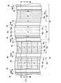
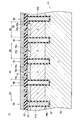
- the top view of the semiconductor substrate of IGBT10 which concerns on embodiment (The figure which abbreviate
- the semiconductor device 10 is an RC-IGBT including an IGBT and a diode.
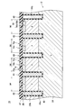
- the semiconductor device 10 includes a semiconductor substrate 12 and electrodes, insulators, and the like formed on the upper and lower surfaces of the semiconductor substrate 12.
- the semiconductor substrate 12 has an IGBT region 90 in which an IGBT is formed and a diode region 92 in which a diode is formed.
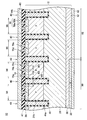
- a plurality of trenches 40 are formed in a concave shape on the upper surface of the semiconductor substrate 12. As shown in FIG. 1, the trenches 40 extend in parallel with each other. The inner surface of each trench 40 is covered with an insulating film 42.
- trench electrodes 44 (44 a and 44 b) are arranged inside each trench 40.
- the trench electrode 44 is insulated from the semiconductor substrate 12 by the insulating film 42.
- Each trench electrode 44a in the IGBT region 90 is connected to a gate wiring at a position not shown.
- Each trench electrode 44 in the diode region 92 is connected to an upper electrode 60 described later at a position not shown.
- the trench electrode 44a connected to the gate wiring may be referred to as a gate electrode 44a
- the trench electrode 44b connected to the upper electrode 60 may be referred to as a control electrode 44b.
- An interlayer insulating film 47 is formed on the upper surface of the semiconductor substrate 12 and on the trench electrode 44. A part of the interlayer insulating film 47 is formed in the regions 94 and 96 sandwiched between the two trenches 40. A part of the interlayer insulating film 47 covers the upper surface of each trench electrode 44.
- a plurality of contact holes 70a to 70e are formed in the interlayer insulating film 47.
- the contact holes 70 a to 70 c are formed in a range 94 sandwiched between two trenches 40 in the IGBT region 90.
- Three contact holes 70a to 70c are formed in each of the regions 94 sandwiched between the two trenches 40 in the IGBT region 90.
- the contact holes 70 d and 70 e are formed in a range 96 sandwiched between the two trenches 40 in the diode region 92. Two contact holes 70 d and 70 e are formed in each of the ranges 96 sandwiched between the two trenches 40 in the diode region 92.
- the hatched area in FIG. 1 indicates the area where the contact holes 70a to 70e are formed.
- the contact holes 70 a to 70 e extend in parallel with the trench 40.
- a conductor layer 74 is formed in each of the contact holes 70a to 70e.
- the conductor layer 74 is made of tungsten. Each conductor layer 74 is connected to the semiconductor substrate 12 at the lower end thereof.
- An upper electrode 60 is formed on the conductor layer 74 and the interlayer insulating film 47.
- the upper electrode 60 is insulated from the trench electrode 44 by the interlayer insulating film 47.
- the upper electrode 60 is connected to the conductor layer 74 in the contact holes 70a to 70e. That is, the upper electrode 60 is connected to the emitter region 20 and the body contact region 21a described later via the conductor layer 74 in the contact holes 70a to 70c.
- the upper electrode 60 is connected to an anode contact region 50a described later via a conductor layer 74 in the contact holes 70d and 70e.
- the connection between the upper electrode 60 and the semiconductor layer via the conductor layer 74 in the contact hole 70 may be referred to as being connected via the contact hole 70.
- the upper electrode 60 is made of aluminum.
- the Young's modulus of the upper electrode 60 ie, aluminum
- the Young's modulus of the conductor layer 74 ie, tungsten).
- a lower electrode 62 is formed on the lower surface of the semiconductor substrate 12.
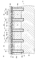
- an emitter region 20 Inside the semiconductor substrate 12 in the IGBT region 90, an emitter region 20, a body region 21, a drift region 28, a buffer region 30 and a collector region 32 are formed.
- the emitter region 20 is an n-type region and is formed in a range exposed on the upper surface of the semiconductor substrate 12.
- the emitter region 20 is connected to the upper electrode 60 through contact holes 70a to 70c. As shown in FIG. 1, the emitter region 20 extends long in a direction orthogonal to the trench electrode 44.
- the emitter region 20 is in contact with the insulating film 42.
- the body region 21 has a body contact region 21a and a low-concentration body region 21b.
- the body contact region 21a is a p-type region containing a high concentration of p-type impurities.
- the body contact region 21 a is formed in a range exposed on the upper surface of the semiconductor substrate 12. As shown in FIG. 1, the body contact region 21 a extends long in a direction perpendicular to the trench electrode 44.
- the body contact region 21 a is adjacent to the emitter region 20.
- Body contact region 21a is connected to upper electrode 60 through contact holes 70a to 70c.
- the low concentration body region 21b is a p-type region having a lower p-type impurity concentration than the body contact region 21a.
- the low concentration body region 21b is formed below the emitter region 20 and the body contact region 21a.
- the low concentration body region 21 b is in contact with the insulating film 42 on the lower side of the emitter region 20.
- the drift region 28 is an n-type region containing an n-type impurity at a lower concentration than the emitter region 20.
- the drift region 28 is formed below the low concentration body region 21b.
- the drift region 28 is separated from the emitter region 20 by the low concentration body region 21b.
- the drift region 28 is in contact with the insulating film 42 below the low-concentration body region 21b.
- the buffer region 30 is an n-type region containing n-type impurities at a higher concentration than the drift region 28.
- the buffer region 30 is formed below the drift region 28.
- the collector region 32 is a p-type region containing a high concentration of p-type impurities.
- the collector region 32 is formed below the buffer region 30.
- the collector region 32 is formed in a range exposed on the lower surface of the semiconductor substrate 12.
- the collector region 32 is connected to the lower electrode 62.
- anode region 50 Inside the semiconductor substrate 12 in the diode region 92, an anode region 50, a drift region 28, and a cathode region 52 are formed.
- the anode region 50 has an anode contact region 50a and a low concentration anode region 50b.
- the anode contact region 50a is a p-type region containing a high concentration of p-type impurities.
- the anode contact region 50 a is formed in a range exposed on the upper surface of the semiconductor substrate 12. As shown in FIG. 1, the anode contact region 50 a extends long in parallel to the trench electrode 44.
- the anode contact region 50a is connected to the upper electrode 60 through contact holes 70d and 70e.
- the low concentration anode region 50b is a p-type region having a lower p-type impurity concentration than the anode contact region 50a. As shown in FIGS. 2 and 3, the low-concentration anode region 50b is formed on the side and the lower side of the anode contact region 50a.
- the drift region 28 described above is formed below the low concentration anode region 50b. That is, part of the drift region 28 is formed below the low concentration anode region 50b. The drift region 28 is in contact with the low concentration anode region 50b.
- the cathode region 52 is an n-type region containing a higher concentration of n-type impurities than the drift region 28.
- the cathode region 52 is formed below the drift region 28 in the diode region 92.
- the cathode region 52 is connected to the buffer region 30. Further, the cathode region 52 is adjacent to the collector region 32.
- the cathode region 52 is formed in a range exposed on the lower surface of the semiconductor substrate 12.
- the cathode region 52 is connected to the lower electrode 62.
- the interval between the trenches 40 is the same in both the IGBT region 90 and the diode region 92. For this reason, when the semiconductor substrate 12 is viewed from above, the area S1 of each range 94 and the area S2 of each range 96 are equal.
- the sizes of the contact holes 70a to 70e are substantially equal. Therefore, the area Sa in which the contact hole 70a is in contact with the semiconductor substrate 12, the area Sb in which the contact hole 70b is in contact with the semiconductor substrate 12, the area Sc in which the contact hole 70c is in contact with the semiconductor substrate 12, and the contact hole The area Sd in which 70d is in contact with the semiconductor substrate 12 and the area Se in which the contact hole 70e is in contact with the semiconductor substrate 12 are equal.
- the ratio of the contact areas of contact holes 70a to 70c to range 94 in IGBT region 90 is larger than the ratio of the contact areas of contact holes 70d and 70e to range 96 in diode region 92. More specifically, the relationship (Sa + Sb + Sc) / S1> (Sd + Se) / S2 is satisfied.
- the operation of the IGBT in the IGBT region 90 will be described.
- a voltage that makes the lower electrode 62 positive is applied between the upper electrode 60 and the lower electrode 62.
- the gate voltage voltage applied to the gate electrode 44a
- the gate threshold minimum gate voltage necessary to turn on the IGBT
- the holes flow from the body contact region 21a to the upper electrode 60 while the IGBT is on, the holes pass through the contact holes 70a to 70c.
- the holes flow dispersedly in the contact holes 70a to 70c. For this reason, it is possible to prevent current from being concentrated in one contact hole. Therefore, for example, when an overvoltage is applied to the IGBT, it is possible to prevent current from concentrating on one contact hole and excessively generating heat around the contact hole. For this reason, the IGBT of the semiconductor device 10 of the embodiment has a high short-circuit tolerance.
- the IGBT of the semiconductor device 10 of the embodiment has a wide range of voltage and current that can be appropriately operated at the time of turn-off, and has high RBSOA tolerance.
- the IGBT of the semiconductor device 10 of the embodiment has a high avalanche resistance.
- the diode in the diode region 92 is turned on. That is, holes flow from the upper electrode 60 to the lower electrode 62 through the anode contact region 50 a, the low concentration anode region 50 b, the drift region 28, and the cathode region 52. Further, electrons flow from the lower electrode 62 to the upper electrode 60 through the cathode region 52, the drift region 28, the low concentration anode region 50b, and the anode contact region 50a. Thereby, a current flows through the diode.
- a voltage that is, forward voltage
- the diode performs a reverse recovery operation. That is, holes existing in the drift region 28 are discharged to the upper electrode 60 through the low concentration anode region 50b and the anode contact region 50a. For this reason, a reverse current instantaneously flows in the diode. When all the holes in the drift region 28 are discharged to the upper electrode 60, the reverse current becomes substantially zero.
- the area where the conductor layer 74 in the contact holes 70d and 70e is in contact with the semiconductor substrate 12 is small. For this reason, there are few holes flowing into the semiconductor substrate 12 from the upper electrode 60 when the diode is on. Therefore, there are few holes present in the drift region 28 of the diode during the reverse recovery operation. For this reason, few holes are discharged to the upper electrode 60 during the reverse recovery operation. Therefore, the reverse current flowing through the diode during the reverse recovery operation is suppressed.
- the plurality of contact holes 70a to 70c are formed in the range 94 of the IGBT region 90, so that the short-circuit withstand capability, RBSOA capability, and avalanche capability of the IGBT are improved. Improvements are being made. Particularly, since the ratio of the contact area is higher in the IGBT region 90 than in the diode region 92, these characteristics are more effectively improved. Further, in the semiconductor device 10 of the present embodiment, the ratio of the contact area is lower in the diode region 92 than in the IGBT region 90, so that the reverse current of the diode is suppressed.
- the Young's modulus of the conductor layer 74 in each contact hole is higher than the Young's modulus of the upper electrode 60.
- the upper electrode 60 may crack due to various stresses. As described above, when the Young's modulus of the conductor layer 74 is high, it is possible to prevent the crack generated in the upper electrode 60 from proceeding to the semiconductor substrate 12 side. Thereby, the reliability of the semiconductor device 10 is improved.
- the width W1 (see FIG. 2) of the interlayer insulating film 47 on each gate electrode 44a is wider than the widths W2 and W3 of the interlayer insulating film 47 on the semiconductor layer. That is, the interval W1 between the contact hole 70c and the contact hole 70a is wider than the interval W2 between the contact hole 70a and the contact hole 70b and the interval W3 between the contact hole 70b and the contact hole 70c.
- the width W1 of the interlayer insulating film 47 on the gate electrode 44a even when the position of the interlayer insulating film 47 is displaced with respect to the gate electrode 44a due to manufacturing errors, the upper surface of the gate electrode 44a is interlayer-insulated.
- the film 47 can be reliably covered. For this reason, it is possible to suppress a decrease in yield due to misalignment of contact holes during manufacturing and poor formation of the trench 40.
- the contact holes 70a to 70c having a narrow width are formed as described above, the layout freedom of the contact holes 70a to 70c can be ensured.
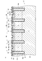
- the semiconductor device 10 is manufactured from an n-type semiconductor substrate (silicon substrate) having substantially the same n-type impurity concentration as the drift region 28. First, the emitter region 20, the body region 21, the drift region 28, the anode region 50, the trench 40, the insulating film 42, and the trench electrode 44 are formed. Next, as shown in FIG. 4, an interlayer insulating film 47 is formed on the semiconductor substrate.
- the interlayer insulating film 47 is selectively etched to form contact holes 70a to 70e in the interlayer insulating film 47 as shown in FIG.
- a conductor layer 74 is formed in the contact hole 70 and on the interlayer insulating film 47.
- the conductor layer 74 is formed by CVD. According to CVD, the conductor layer 74 can be formed in the contact hole 70 without a gap.
- the conductor layer 74 on the interlayer insulating film 47 is removed by etching.
- the conductor layer 74 is left in the contact hole 70.
- the upper surface of the interlayer insulating film 47 and the upper surface of the conductor layer 74 are configured to be substantially in the same plane. That is, the upper surface of the substrate is flattened.
- the upper surface of the conductor layer 74 in the contact hole is formed in a concave shape when the conductor layer 74 is etched. This is because the conductor layer 74 is more easily etched at the center of the contact hole.
- the width of the contact hole 70 is narrow, the upper surface of the conductor layer 74 can be formed substantially flat by etching. For this reason, the upper surface of the substrate can be formed flat.
- the upper electrode 60 is formed on the interlayer insulating film 47 and the conductor layer 74. Since the upper surface of the substrate before the formation of the upper electrode 60 is flat, the upper surface of the upper electrode 60 becomes flat after the upper electrode 60 is formed.
- the upper surface of the upper electrode 60 can be formed flat.
- the upper electrode 60 can be suitably connected to an external electrode or the like using solder, a bonding wire, or the like.
- the conductor layer 74 is formed by CVD, but the conductor layer 74 may be formed by plating or sputtering. That is, the conductor layer 74 may be made of any material as long as it can be formed by CVD, plating, or sputtering.
- the conductor layer 74 can be made of W, Al, Cu, or an alloy containing these.
- two contact holes 70d and 70e are formed in each range 96 sandwiched between the two trenches 40 of the diode region 92.
- one contact hole is formed in each range 96.
- three or more contact holes may be formed in each range 96. Even in this case, as described above, it is preferable that the ratio of the contact area of the contact hole is larger in the IGBT region 90 than in the diode region 92.
- each component of the semiconductor device 10 of said embodiment has the following relationship with respect to each component of a claim.
- the emitter region 20 of the embodiment is an example of a first semiconductor layer in the claims.
- the body region 21 of the embodiment is an example of a second semiconductor layer in the claims.
- the drift region 28 and the buffer region 30 in the embodiment are an example of a third semiconductor layer in the claims.
- the conductor layer 74 in the IGBT region 90 of the embodiment is an example of a first conductor layer in the claims.
- the upper electrode 60 of the embodiment is an example of a surface electrode in the claims.
- the range 94 of the embodiment is an example of a first range of the claims.
- the anode region 50 of the embodiment is an example of a fourth semiconductor layer in the claims.
- the conductor layer 74 in the diode region 92 of the embodiment is an example of a second conductor layer in the claims.
- the semiconductor device 10 has the collector region 32.
- the collector region 32 may be omitted.
- the MOSFET is formed by connecting the buffer region 30 to the lower electrode.
- the semiconductor device 10 has the diode region 92, but the diode region 92 may not be formed.
- the configuration of the semiconductor device 10 of the embodiment can be expressed as follows.
- a semiconductor device having a semiconductor substrate, wherein a plurality of trenches formed on an upper surface of the semiconductor substrate, a trench insulating film covering an inner surface of each trench, and the trench insulation are disposed inside each trench.
- a trench electrode insulated from the semiconductor substrate by a film and the semiconductor substrate in a first range sandwiched between adjacent trenches of the plurality of trenches, and exposed on the upper surface of the semiconductor substrate And a first conductive type first semiconductor layer in contact with the trench insulating film, and the first semiconductor layer in the first range, a part of which is exposed on the upper surface of the semiconductor substrate.
- a second conductive type second semiconductor layer that is in contact with the trench insulating film under the first semiconductor layer, and is formed on the semiconductor substrate.
- a third semiconductor layer of a first conductivity type disposed on a side of the first semiconductor layer and separated from the first semiconductor layer by the second semiconductor layer and in contact with the trench insulating film below the second semiconductor layer
- an interlayer insulating film having a plurality of contact holes disposed in the first range, disposed on the upper surface of the semiconductor substrate and the trench electrode, and disposed in each of the contact holes,
- a first conductor layer connected to at least one of the first semiconductor layer and the second semiconductor layer; and disposed on the first conductor layer and the interlayer insulating film; It has a surface electrode connected to the body layer.
- the semiconductor device is formed on the semiconductor substrate in a second range which is a range sandwiched between adjacent trenches of the plurality of trenches different from the first range, and the upper surface of the semiconductor substrate
- the semiconductor device may further include a first conductive type fourth semiconductor layer exposed to the second conductive layer and a second conductive layer. A part of the third semiconductor layer is disposed below the fourth semiconductor layer, is in contact with the fourth semiconductor layer, and the interlayer insulating film is a contact disposed within the second range.
- the second conductor layer is disposed in the contact hole in the second range, connected to the fourth semiconductor layer, and a portion of the surface electrode is
- the contact area of the plurality of first conductor layers with respect to the semiconductor substrate, which is disposed on the second conductor layer and connected to the second conductor layer, is divided by the area of the first range.
- the value may be larger than a value obtained by dividing a contact area of the second conductor layer with respect to the semiconductor substrate by an area of the second range.
- the characteristics of the switching element formed in the first range can be improved.
- the reverse recovery characteristic of the diode formed in the second range can be improved by reducing the contact area in the second range.
- the Young's modulus of the first conductor layer may be higher than the Young's modulus of the surface electrode.
- the first conductor layer and the second conductor layer may be made of a material that can be formed by CVD, plating, or sputtering.
- the conductor layer can be suitably formed in the contact hole.
- the first conductor layer and the second conductor layer may be made of a metal containing any one of W, Al, and Cu.
- the width of the interlayer insulating film on each trench electrode may be wider than the width of the interlayer insulating film located between the contact holes in the first range.
- the semiconductor device manufacturing method of the embodiment is a method for manufacturing a semiconductor device from a processing wafer, and has the following configuration.
- the processing wafer is disposed in a semiconductor substrate having a plurality of trenches formed on an upper surface, a trench insulating film covering an inner surface of each trench, and the inside of each trench, and the semiconductor substrate is formed by the trench insulating film.
- the semiconductor substrate is formed in a range sandwiched between adjacent trenches of the plurality of trenches, is exposed on the upper surface of the semiconductor substrate, and is in contact with the trench insulating film
- a first semiconductor layer of the mold formed within the range, a part of which is exposed on the upper surface of the semiconductor substrate, and is in contact with the trench insulating film below the first semiconductor layer
- a second-conductivity-type second semiconductor layer disposed below the second semiconductor layer, separated from the first semiconductor layer by the second semiconductor layer, and below the second semiconductor layer;
- the method includes a step of forming an interlayer insulating film on an upper surface of the processing wafer, a step of forming a plurality of contact holes in the interlayer insulating film within the range, and a plurality of contact holes and the interlayers.
- the surface electrode can be flattened and a wide contact area of the surface electrode can be secured.
Landscapes
- Engineering & Computer Science (AREA)
- Power Engineering (AREA)
- Microelectronics & Electronic Packaging (AREA)
- Physics & Mathematics (AREA)
- Condensed Matter Physics & Semiconductors (AREA)
- General Physics & Mathematics (AREA)
- Computer Hardware Design (AREA)
- Ceramic Engineering (AREA)
- Manufacturing & Machinery (AREA)
- Geometry (AREA)
- Electrodes Of Semiconductors (AREA)
- Internal Circuitry In Semiconductor Integrated Circuit Devices (AREA)
Abstract
【課題】 半導体装置は、半導体基板の上面に形成された複数のトレンチと、各トレンチの内部に配置されたトレンチ電極と、複数のトレンチのうちの隣り合うトレンチに挟まれた第1範囲内に形成された第1導電型の第1半導体層、第2導電型の第2半導体層及び第1導電型の第3半導体層と、半導体基板の上面に配置され、第1範囲内に複数のコンタクトホールを有する層間絶縁膜と、各コンタクトホール内に形成されている第1導電体層と、層間絶縁膜上に配置されており、各第1導電体層に接続されている表面電極を有する。
Description
(関連出願の相互参照)
本出願は、2014年8月6日に出願された日本特許出願特願2014-160719の関連出願であり、この日本特許出願に基づく優先権を主張するものであり、この日本特許出願に記載された全ての内容を、本明細書を構成するものとして援用する。
本出願は、2014年8月6日に出願された日本特許出願特願2014-160719の関連出願であり、この日本特許出願に基づく優先権を主張するものであり、この日本特許出願に記載された全ての内容を、本明細書を構成するものとして援用する。
本明細書が開示する技術は、IGBT、MOSFETなどの半導体装置に関する。
国際公開第2013/121519号公報(以下、特許文献1という)には、トレンチ型のゲート電極を有するスイッチング用の半導体装置が開示されている。この半導体装置は、ゲート電極の上部に形成された層間絶縁膜を有している。半導体基板の上面の略全域には、層間絶縁膜を覆うように表面電極が形成されている。層間絶縁膜によって、ゲート電極が表面電極から絶縁されている。
特許文献1では、隣接する一対のゲート電極に挟まれた範囲の半導体層上に層間絶縁膜が形成されていない。表面電極は、層間絶縁膜が形成されていない範囲において、半導体基板に接続されている。すなわち、ゲート電極に挟まれた範囲の略全体がコンタクトホールとなっており、この範囲の略全体で表面電極と半導体基板が接触している。この構造では、層間絶縁膜の上部の表面電極がその周囲の表面電極に対して突出し、表面電極の表面に凹凸が形成されてしまう。したがって、本明細書では、表面電極の凹凸を抑制することが可能な半導体装置を提供する。
表面電極の凹凸を解消するための手法として、表面電極をエッチバックすることが考えられる。すなわち、表面電極をその表面側からエッチバックして、コンタクトホール内にのみ表面電極を残存させる。そして、その後に、コンタクトホール内の電極上と層間絶縁膜上に再度電極を成長させる。しかしながら、この手法では、コンタクトホールが大きいため、コンタクトホールの中央でエッチング速度が速くなり、エッチバックを実施した後にコンタクトホールの中央部で電極の表面が窪んでしまう。このため、その後に再度電極を成長させても、電極表面に凹部が残ってしまう。この問題を解決するために、層間絶縁膜の幅を広くして、コンタクトホールを小さくすることが考えられる。コンタクトホールを小さくすれば、上記の窪みが生じ難い。しかしながら、コンタクトホールを小さくすると、表面電極と半導体基板との間のコンタクト面積が小さくなり、コンタクト部に電流が集中するという問題が生じる。
これに対し、本明細書が開示する半導体装置は、以下の構成を有する。この半導体装置は、半導体基板を有する。この半導体装置は、前記半導体基板の上面に形成された複数のトレンチと、前記各トレンチの内面を覆うトレンチ絶縁膜と、前記各トレンチの内部に配置されており、前記トレンチ絶縁膜によって前記半導体基板から絶縁されているトレンチ電極と、前記複数のトレンチのうちの隣り合うトレンチに挟まれた第1範囲内の前記半導体基板に形成されており、前記半導体基板の前記上面に露出しており、前記トレンチ絶縁膜に接している第1導電型の第1半導体層と、前記第1範囲内の前記半導体基板に形成されており、一部が前記半導体基板の前記上面に露出しており、前記第1半導体層の下側で前記トレンチ絶縁膜に接している第2導電型の第2半導体層と、前記半導体基板に形成されており、前記第2半導体層の下側に配置されており、前記第2半導体層によって前記第1半導体層から分離されており、前記第2半導体層の下側で前記トレンチ絶縁膜に接している第1導電型の第3半導体層と、前記半導体基板の前記上面及び前記トレンチ電極上に配置されており、前記第1範囲内に配置された複数のコンタクトホールを有する層間絶縁膜と、前記各コンタクトホール内に配置されており、前記第1半導体層と前記第2半導体層の少なくとも一方に接続されている第1導電体層と、前記第1導電体層上及び前記層間絶縁膜上に配置されており、前記各第1導電体層に接続されている表面電極を有する。
この半導体装置では、トレンチに挟まれた第1範囲内に複数のコンタクトホールが設けられているので、各コンタクトホールのサイズが小さい。各コンタクトホールのサイズが小さいので、表面電極の表面の凹凸を抑制することができる。また、この半導体装置では、半導体基板と表面電極とが複数のコンタクトホールを介して接続されている。したがって、第1範囲内にサイズが小さい単一のコンタクトホールが形成されている場合に比べて、表面電極の半導体基板に対するコンタクト面積を広く確保することができる。このため、1つのコンタクトホールに電流が集中することを防止することができる。
上記の半導体装置によれば、表面電極の平坦化が可能であり、かつ、表面電極の広いコンタクト面積を確保することができる。
図1~3に示す実施形態に係る半導体装置10は、IGBTとダイオードを備えるRC-IGBTである。半導体装置10は、半導体基板12と、半導体基板12の上面及び下面に形成された電極、絶縁体等によって構成されている。半導体基板12は、IGBTが形成されているIGBT領域90と、ダイオードが形成されているダイオード領域92を有している。
図2、3に示すように、半導体基板12の上面には、複数のトレンチ40が凹状に形成されている。図1に示すように、各トレンチ40は、互いに平行に伸びている。各トレンチ40の内面は、絶縁膜42に覆われている。
図2、3に示すように、各トレンチ40の内部には、トレンチ電極44(44a、44b)が配置されている。トレンチ電極44は、絶縁膜42によって半導体基板12から絶縁されている。IGBT領域90内の各トレンチ電極44aは、図示しない位置でゲート配線に接続されている。ダイオード領域92内の各トレンチ電極44は、図示しない位置で後述する上部電極60に接続されている。以下では、ゲート配線に接続されているトレンチ電極44aをゲート電極44aと呼び、上部電極60に接続されているトレンチ電極44bを制御電極44bという場合がある。
半導体基板12の上面及びトレンチ電極44上には、層間絶縁膜47が形成されている。層間絶縁膜47の一部は、2つのトレンチ40に挟まれた範囲94、96内に形成されている。また、層間絶縁膜47の一部は、各トレンチ電極44の上面を覆っている。層間絶縁膜47には、複数のコンタクトホール70a~70eが形成されている。コンタクトホール70a~70cは、IGBT領域90内の2つのトレンチ40に挟まれた範囲94に形成されている。IGBT領域90内の2つのトレンチ40に挟まれた範囲94のそれぞれに、3つのコンタクトホール70a~70cが形成されている。コンタクトホール70d、70eは、ダイオード領域92内の2つのトレンチ40に挟まれた範囲96に形成されている。ダイオード領域92内の2つのトレンチ40に挟まれた範囲96のそれぞれに、2つのコンタクトホール70d、70eが形成されている。図1の斜線によりハッチングされた範囲は、コンタクトホール70a~70eが形成されている範囲を示している。図1に示すように、コンタクトホール70a~70eは、トレンチ40と平行に伸びている。図2、3に示すように、各コンタクトホール70a~70eの内部には、導電体層74が形成されている。導電体層74は、タングステンにより構成されている。各導電体層74は、その下端において半導体基板12に接続されている。
導電体層74上及び層間絶縁膜47上には、上部電極60が形成されている。上部電極60は、層間絶縁膜47によってトレンチ電極44から絶縁されている。また、上部電極60は、コンタクトホール70a~70e内の導電体層74に接続されている。すなわち、上部電極60は、コンタクトホール70a~70c内の導電体層74を介して、後述するエミッタ領域20及びボディコンタクト領域21aに接続されている。また、上部電極60は、コンタクトホール70d、70e内の導電体層74を介して、後述するアノードコンタクト領域50aに接続されている。なお、以下では、上部電極60と半導体層とがコンタクトホール70内の導電体層74を介して接続されていることを、これらがコンタクトホール70を介して接続されているという場合がある。上部電極60は、アルミニウムにより構成されている。上部電極60(すなわち、アルミニウム)のヤング率は、導電体層74(すなわち、タングステン)のヤング率よりも低い。
半導体基板12の下面には、下部電極62が形成されている。
IGBT領域90内の半導体基板12の内部には、エミッタ領域20、ボディ領域21、ドリフト領域28、バッファ領域30及びコレクタ領域32が形成されている。
エミッタ領域20は、n型領域であり、半導体基板12の上面に露出する範囲に形成されている。エミッタ領域20は、コンタクトホール70a~70cを介して上部電極60に接続されている。図1に示すように、エミッタ領域20は、トレンチ電極44に直交する方向に長く伸びている。エミッタ領域20は、絶縁膜42に接している。
図2、3に示すように、ボディ領域21は、ボディコンタクト領域21aと低濃度ボディ領域21bを有している。ボディコンタクト領域21aは、高濃度のp型不純物を含有するp型領域である。ボディコンタクト領域21aは、半導体基板12の上面に露出する範囲に形成されている。図1に示すように、ボディコンタクト領域21aは、トレンチ電極44に直交する方向に長く伸びている。ボディコンタクト領域21aは、エミッタ領域20に隣接している。ボディコンタクト領域21aは、コンタクトホール70a~70cを介して上部電極60に接続されている。
低濃度ボディ領域21bは、ボディコンタクト領域21aよりもp型不純物濃度が低いp型領域である。低濃度ボディ領域21bは、エミッタ領域20とボディコンタクト領域21aの下側に形成されている。低濃度ボディ領域21bは、エミッタ領域20の下側において、絶縁膜42に接している。
ドリフト領域28は、エミッタ領域20よりも低濃度のn型不純物を含有するn型領域である。ドリフト領域28は、低濃度ボディ領域21bの下側に形成されている。ドリフト領域28は、低濃度ボディ領域21bによってエミッタ領域20から分離されている。ドリフト領域28は、低濃度ボディ領域21bの下側において絶縁膜42と接している。
バッファ領域30は、ドリフト領域28よりも高濃度のn型不純物を含有するn型領域である。バッファ領域30は、ドリフト領域28の下側に形成されている。
コレクタ領域32は、高濃度のp型不純物を含有するp型領域である。コレクタ領域32は、バッファ領域30の下側に形成されている。コレクタ領域32は、半導体基板12の下面に露出する範囲に形成されている。コレクタ領域32は、下部電極62に接続されている。
ダイオード領域92内の半導体基板12の内部には、アノード領域50と、ドリフト領域28と、カソード領域52が形成されている。
アノード領域50は、アノードコンタクト領域50aと低濃度アノード領域50bを有している。アノードコンタクト領域50aは、高濃度のp型不純物を含有するp型領域である。アノードコンタクト領域50aは、半導体基板12の上面に露出する範囲に形成されている。図1に示すように、アノードコンタクト領域50aは、トレンチ電極44に対して平行に長く伸びている。アノードコンタクト領域50aは、コンタクトホール70d、70eを介して上部電極60に接続されている。
低濃度アノード領域50bは、アノードコンタクト領域50aよりもp型不純物濃度が低いp型領域である。図2、3に示すように、低濃度アノード領域50bは、アノードコンタクト領域50aの側方と下側に形成されている。
低濃度アノード領域50bの下側には、上述したドリフト領域28が形成されている。すなわち、ドリフト領域28の一部は、低濃度アノード領域50bの下側に形成されている。ドリフト領域28は、低濃度アノード領域50bに接している。
カソード領域52は、ドリフト領域28よりも高濃度のn型不純物を含有するn型領域である。カソード領域52は、ダイオード領域92内のドリフト領域28の下側に形成されている。カソード領域52は、バッファ領域30と繋がっている。また、カソード領域52は、コレクタ領域32に隣接している。カソード領域52は、半導体基板12の下面に露出する範囲に形成されている。カソード領域52は、下部電極62に接続されている。
トレンチ40の間の間隔は、IGBT領域90とダイオード領域92のいずれにおいても等しい。このため、半導体基板12を上から平面視したときに、各範囲94の面積S1と各範囲96の面積S2は等しい。また、各コンタクトホール70a~70eのサイズは、略等しい。このため、コンタクトホール70aが半導体基板12にコンタクトしている面積Sa、コンタクトホール70bが半導体基板12にコンタクトしている面積Sb、コンタクトホール70cが半導体基板12にコンタクトしている面積Sc、コンタクトホール70dが半導体基板12にコンタクトしている面積Sd、及び、コンタクトホール70eが半導体基板12にコンタクトしている面積Seは等しい。また、上述したように、IGBT領域90内では、2つのトレンチ40に挟まれた範囲94内に3つのコンタクトホール70a~70cが形成されているのに対し、ダイオード領域92内では、2つのトレンチ40に挟まれた範囲96内に2つのコンタクトホール70d、70eが形成されている。したがって、IGBT領域90内の範囲94に対するコンタクトホール70a~70cのコンタクト面積の割合は、ダイオード領域92内の範囲96に対するコンタクトホール70d、70eのコンタクト面積の割合よりも大きい。より詳細には、(Sa+Sb+Sc)/S1>(Sd+Se)/S2の関係が満たされている。
次に、IGBT領域90内のIGBTの動作について説明する。IGBTの動作時には、上部電極60と下部電極62との間に下部電極62がプラスになる電圧が印加される。この状態で、ゲート電圧(ゲート電極44aへの印加電圧)をゲート閾値(IGBTをオンさせるのに必要最小限のゲート電圧)以上に上昇させると、IGBTがオンする。すなわち、ゲート電極44aへの電圧の印加によって、低濃度ボディ領域21bの絶縁膜42と接する範囲にチャネルが形成さる。これによって、電子が、上部電極60から、エミッタ領域20、低濃度ボディ領域21bのチャネル、ドリフト領域28、バッファ領域30、及び、コレクタ領域32を介して、下部電極62へ流れる。また、ホールが、下部電極62から、コレクタ領域32、バッファ領域30、ドリフト領域28、低濃度ボディ領域21b、及び、ボディコンタクト領域21aを介して、上部電極60へ流れる。これによって、IGBTに電流が流れる。
IGBTがオンしている間にホールがボディコンタクト領域21aから上部電極60へ流れる際に、ホールはコンタクトホール70a~70cを通過する。このように、複数のコンタクトホール70a~70cを介してボディコンタクト領域21aから上部電極60へホールが流れるため、各コンタクトホール70a~70cに分散してホールが流れる。このため、1つのコンタクトホールに電流が集中することを防止することができる。したがって、例えば、IGBTに過電圧が印加された場合に、1つのコンタクトホールに電流が集中してそのコンタクトホール周辺が過度に発熱することを防止することができる。このため、実施形態の半導体装置10のIGBTは、短絡耐量が高い。
ゲート電圧をゲート閾値未満に低下させると、チャネルが消失し、IGBTがターンオフする。このとき、ドリフト領域28内に存在するホールが、低濃度ボディ領域21bとボディコンタクト領域21aを介して上部電極60に排出される。この場合に、ホールが複数のコンタクトホール70a~70cを通って上部電極60へ流れる。このため、1つのコンタクトホールに電流が集中することを防止することができる。したがって、実施形態の半導体装置10のIGBTは、ターンオフ時に適切に動作可能な電圧と電流の範囲が広く、RBSOA耐量が高い。
また、IGBTがターンオフする際やIGBTがオフしている際に、上部電極60と下部電極62の間に過電圧が印加されると、IGBT領域90内のドリフト領域28内で高い電界によりホールが生成される場合がある。この場合、ホールが複数のコンタクトホール70a~70cを通って上部電極60へ流れる。このため、発生したホールを短時間で上部電極60に排出することが可能であり、ドリフト領域28内でアバランシェ降伏が生じることを抑制することができる。このため、実施形態の半導体装置10のIGBTは、アバランシェ耐量が高い。
次に、ダイオードの動作について説明する。上部電極60と下部電極62との間に上部電極60がプラスになる電圧(すなわち、順電圧)が印加されると、ダイオード領域92内のダイオードがオンする。すなわち、ホールが、上部電極60から、アノードコンタクト領域50a、低濃度アノード領域50b、ドリフト領域28、及び、カソード領域52を介して、下部電極62へ流れる。また、電子が、下部電極62から、カソード領域52、ドリフト領域28、低濃度アノード領域50b、及び、アノードコンタクト領域50aを介して、上部電極60へ流れる。これによって、ダイオードに電流が流れる。その後、ダイオードへの印加電圧が順電圧から逆電圧に切り換えられると、ダイオードが逆回復動作を行う。すなわち、ドリフト領域28内に存在するホールが、低濃度アノード領域50bとアノードコンタクト領域50aを介して、上部電極60に排出される。このため、ダイオードには瞬間的に逆電流が流れる。ドリフト領域28内の全てのホールが上部電極60に排出されると、逆電流は略ゼロとなる。
本実施形態の半導体装置10では、コンタクトホール70d、70e内の導電体層74が半導体基板12にコンタクトしている面積が小さい。このため、ダイオードがオンしているときに、上部電極60から半導体基板12に流入するホールが少ない。したがって、逆回復動作時にダイオードのドリフト領域28内に存在するホールが少ない。このため、逆回復動作の間に上部電極60に排出されるホールが少ない。したがって、逆回復動作時にダイオードに流れる逆電流が抑制される。
以上に説明したように、本実施形態の半導体装置10では、IGBT領域90の範囲94内に複数のコンタクトホール70a~70cが形成されていることで、IGBTの短絡耐量、RBSOA耐量及びアバランシェ耐量の向上が図られている。特に、IGBT領域90内ではダイオード領域92内よりもコンタクト面積の割合が高くなっていることで、これらの特性がより効果的に向上されている。また、本実施形態の半導体装置10では、ダイオード領域92内ではIGBT領域90内よりもコンタクト面積の割合が低くなっていることで、ダイオードの逆電流が抑制される。
また、上述した実施形態の半導体装置10では、各コンタクトホール内の導電体層74のヤング率が、上部電極60のヤング率よりも高い。上部電極60には、種々のストレスによりクラックが生じる場合がある。上記のように導電体層74のヤング率が高いと、上部電極60で生じたクラックが、半導体基板12側に進行することを抑制することができる。これによって、半導体装置10の信頼性が向上されている。
また、各ゲート電極44a上の層間絶縁膜47の幅W1(図2参照)は、半導体層上の層間絶縁膜47の幅W2、W3よりも広い。すなわち、コンタクトホール70cとコンタクトホール70aの間の間隔W1は、コンタクトホール70aとコンタクトホール70bの間の間隔W2及びコンタクトホール70bとコンタクトホール70cの間の間隔W3よりも広い。このようにゲート電極44a上の層間絶縁膜47の幅W1を広くすることで、製造誤差により層間絶縁膜47の位置がゲート電極44aに対してずれた場合でも、ゲート電極44aの上面を層間絶縁膜47で確実に覆うことができる。このため、製造時におけるコンタクトホールの位置合わせのずれやトレンチ40の形成不良による歩留まり低下を抑制することができる。
また、上記のように幅が狭いコンタクトホール70a~70cが形成されていることで、コンタクトホール70a~70cのレイアウト自由度を確保することができる。
(製造工程)
次に、半導体装置10の製造方法を説明する。半導体装置10は、ドリフト領域28と略同じn型不純物濃度を有するn型の半導体基板(シリコン基板)から製造される。まず、エミッタ領域20、ボディ領域21、ドリフト領域28、アノード領域50、トレンチ40、絶縁膜42、トレンチ電極44を形成する。次に、図4に示すように、半導体基板上に層間絶縁膜47を形成する。
次に、半導体装置10の製造方法を説明する。半導体装置10は、ドリフト領域28と略同じn型不純物濃度を有するn型の半導体基板(シリコン基板)から製造される。まず、エミッタ領域20、ボディ領域21、ドリフト領域28、アノード領域50、トレンチ40、絶縁膜42、トレンチ電極44を形成する。次に、図4に示すように、半導体基板上に層間絶縁膜47を形成する。
次に、層間絶縁膜47を選択的にエッチングすることによって、図5に示すように、層間絶縁膜47にコンタクトホール70a~70eを形成する。
次に、図6に示すように、コンタクトホール70内及び層間絶縁膜47上に導電体層74を形成する。導電体層74は、CVDにより形成する。CVDによれば、コンタクトホール70内に隙間なく導電体層74を形成することができる。
次に、層間絶縁膜47上の導電体層74をエッチングすることにより除去する。ここでは、図7に示すように、コンタクトホール70内に導電体層74を残存させる。これによって、層間絶縁膜47の上面と導電体層74の上面が略同一平面を構成するようにする。すなわち、基板の上面を平坦化する。
なお、仮にコンタクトホールの幅が広い場合には、導電体層74をエッチングする際に、コンタクトホール内の導電体層74の上面が凹状に成形される。これは、コンタクトホールの中央部では導電体層74がよりエッチングされ易いためである。しかしながら、本実施形態では、コンタクトホール70の幅が狭いため、エッチングにより導電体層74の上面を略平坦に成形することができる。このため、基板の上面を平坦に成形することができる。
次に、図8に示すように、層間絶縁膜47及び導電体層74上に、上部電極60を形成する。上部電極60の形成前の基板の上面が平坦であるので、上部電極60を形成後に上部電極60の上面が平坦となる。
その後、下面側の構造を形成することで、図1~3に示す半導体装置10が完成する。
以上に説明したように、本実施形態の半導体装置10の構造及び製造方法によれば、上部電極60の上面を平坦に成形することができる。このため、上部電極60を外部の電極等に対してはんだやボンディングワイヤー等を用いて好適に接続することができる。
なお、上述した実施形態では、導電体層74をCVDにより形成したが、メッキやスパッタリングによって導電体層74を形成してもよい。すなわち、導電体層74は、CVD、メッキまたはスパッタリングにより形成可能な導電材料であれば、いずれの材料によって構成されていてもよい。例えば、導電体層74は、W、Al、Cuまたはこれらを含む合金によって構成され得る。
なお、実施形態の半導体装置10では、ダイオード領域92の2つのトレンチ40に挟まれた各範囲96に2つのコンタクトホール70d、70eが形成されていたが、各範囲96に1つのコンタクトホールが形成されていてもいし、各範囲96に3つ以上のコンタクトホールが形成されていてもよい。この場合でも、上述したように、コンタクトホールのコンタクト面積の割合をIGBT領域90でダイオード領域92よりも大きくすることが好ましい。
なお、上記の実施形態の半導体装置10の各構成要素は、請求項の各構成要素に対して以下の関係を有する。実施形態のエミッタ領域20は、請求項の第1半導体層の一例である。実施形態のボディ領域21は、請求項の第2半導体層の一例である。実施形態のドリフト領域28及びバッファ領域30は、請求項の第3半導体層の一例である。実施形態のIGBT領域90内の導電体層74は、請求項の第1導電体層の一例である。実施形態の上部電極60は、請求項の表面電極の一例である。実施形態の範囲94は、請求項の第1範囲の一例である。実施形態のアノード領域50は、請求項の第4半導体層の一例である。実施形態のダイオード領域92内の導電体層74は、請求項の第2導電体層の一例である。
なお、上述した実施形態では、半導体装置10がコレクタ領域32を有していたが、コレクタ領域32を省略してもよい。この場合、バッファ領域30が下部電極に接続されることにより、MOSFETが形成される。
また、上述した実施形態では半導体装置10がダイオード領域92を有していたが、ダイオード領域92は形成されていなくてもよい。
実施形態の半導体装置10の構成は、以下のように表すことができる。
半導体基板を有する半導体装置であって、前記半導体基板の上面に形成された複数のトレンチと、前記各トレンチの内面を覆うトレンチ絶縁膜と、前記各トレンチの内部に配置されており、前記トレンチ絶縁膜によって前記半導体基板から絶縁されているトレンチ電極と、前記複数のトレンチのうちの隣り合うトレンチに挟まれた第1範囲内の前記半導体基板に形成されており、前記半導体基板の前記上面に露出しており、前記トレンチ絶縁膜に接している第1導電型の第1半導体層と、前記第1範囲内の前記半導体基板に形成されており、一部が前記半導体基板の前記上面に露出しており、前記第1半導体層の下側で前記トレンチ絶縁膜に接している第2導電型の第2半導体層と、前記半導体基板に形成されており、前記第2半導体層の下側に配置されており、前記第2半導体層によって前記第1半導体層から分離されており、前記第2半導体層の下側で前記トレンチ絶縁膜に接している第1導電型の第3半導体層と、前記半導体基板の前記上面及び前記トレンチ電極上に配置されており、前記第1範囲内に配置された複数のコンタクトホールを有する層間絶縁膜と、前記各コンタクトホール内に配置されており、前記第1半導体層と前記第2半導体層の少なくとも一方に接続されている第1導電体層と、前記第1導電体層上及び前記層間絶縁膜上に配置されており、前記各第1導電体層に接続されている表面電極を有する。
上記の半導体装置は、前記第1範囲とは異なる前記複数のトレンチのうちの隣り合うトレンチに挟まれた範囲である第2範囲内の前記半導体基板に形成されており、前記半導体基板の前記上面に露出している第1導電型の第4半導体層と、第2導電体層をさらに有していてもよい。前記第3半導体層の一部が、前記第4半導体層の下側に配置されており、前記第4半導体層に接しており、前記層間絶縁膜が、前記第2範囲内に配置されたコンタクトホールを有しており、前記第2導電体層が、前記第2範囲内の前記コンタクトホール内に配置されており、前記第4半導体層に接続されており、前記表面電極の一部が、前記第2導電体層上に配置されており、前記第2導電体層に接続されており、前記複数の第1導電体層の前記半導体基板に対するコンタクト面積を前記第1範囲の面積で除算した値が、前記第2導電体層の前記半導体基板に対するコンタクト面積を前記第2範囲の面積で除算した値よりも大きくてもよい。
このように第1範囲におけるコンタクト面積を大きくすることで、第1範囲に形成されたスイッチング素子の特性を向上させることができる。また、第2範囲におけるコンタクト面積を小さくすることで、第2範囲に形成されたダイオードの逆回復特性を向上させることができる。
第1導電体層のヤング率は、表面電極のヤング率よりも高くてもよい。
このように構成されていることによって、ストレスにより表面電極にクラックが生じた場合であっても、そのクラックが半導体基板側に進展することを抑制することができる。
第1導電体層及び第2導電体層は、CVD、メッキ、スパッタによって形成可能な材料によって構成されていてもよい。
このように構成されていることによって、コンタクトホール内に好適に導電体層を形成することができる。
第1導電体層及び第2導電体層は、W、Al、Cuのいずれかを含む金属によって構成されていてもよい。
各トレンチ電極上の層間絶縁膜の幅が、前記第1範囲内のコンタクトホールの間に位置する前記層間絶縁膜の幅よりも広くてもよい。
また、実施形態の半導体装置の製造方法は、加工用ウエハから半導体装置を製造する方法であって、以下の構成を有する。前記加工用ウエハが、上面に複数のトレンチが形成された半導体基板と、前記各トレンチの内面を覆うトレンチ絶縁膜と、前記各トレンチの内部に配置されており、前記トレンチ絶縁膜によって前記半導体基板から絶縁されているトレンチ電極を有している。前記半導体基板が、前記複数のトレンチのうちの隣り合うトレンチに挟まれた範囲内に形成されており、前記半導体基板の前記上面に露出しており、前記トレンチ絶縁膜に接している第1導電型の第1半導体層と、前記範囲内に形成されており、一部が前記半導体基板の前記上面に露出しており、前記第1半導体層の下側で前記トレンチ絶縁膜に接している第2導電型の第2半導体層と、前記第2半導体層の下側に配置されており、前記第2半導体層によって前記第1半導体層から分離されており、前記第2半導体層の下側で前記トレンチ絶縁膜に接している第1導電型の第3半導体層を有している。前記方法が、前記加工用ウエハの上面に、層間絶縁膜を形成する工程と、前記範囲内の前記層間絶縁膜に、複数のコンタクトホールを形成する工程と、前記複数のコンタクトホール内及び前記層間絶縁膜上に、導電体層を成長させる工程と、前記複数のコンタクトホール内に前記導電体層が残存するように前記層間絶縁膜上の前記導電体層をエッチングする工程と、前記エッチングの後に、前記導電体層上及び前記層間絶縁膜上に、表面電極を形成する工程を有している。
このような製造方法をとることによって、表面電極の平坦化が可能であり、かつ、表面電極の広いコンタクト面積を確保することができる。
以上、実施形態について詳細に説明したが、これらは例示にすぎず、特許請求の範囲を限定するものではない。特許請求の範囲に記載の技術には、以上に例示した具体例をさまざまに変形、変更したものが含まれる。本明細書または図面に説明した技術要素は、単独あるいは各種の組み合わせによって技術有用性を発揮するものであり、出願時請求項記載の組み合わせに限定されるものではない。また、本明細書または図面に例示した技術は複数目的を同時に達成するものであり、そのうちの1つの目的を達成すること自体で技術有用性を持つものである。
Claims (7)
- 半導体基板を有する半導体装置であって、
前記半導体基板の上面に形成された複数のトレンチと、
前記各トレンチの内面を覆うトレンチ絶縁膜と、
前記各トレンチの内部に配置されており、前記トレンチ絶縁膜によって前記半導体基板から絶縁されているトレンチ電極と、
前記複数のトレンチのうちの隣り合うトレンチに挟まれた第1範囲内の前記半導体基板に形成されており、前記半導体基板の前記上面に露出しており、前記トレンチ絶縁膜に接している第1導電型の第1半導体層と、
前記第1範囲内の前記半導体基板に形成されており、一部が前記半導体基板の前記上面に露出しており、前記第1半導体層の下側で前記トレンチ絶縁膜に接している第2導電型の第2半導体層と、
前記半導体基板に形成されており、前記第2半導体層の下側に配置されており、前記第2半導体層によって前記第1半導体層から分離されており、前記第2半導体層の下側で前記トレンチ絶縁膜に接している第1導電型の第3半導体層と、
前記半導体基板の前記上面及び前記トレンチ電極上に配置されており、前記第1範囲内に配置された複数のコンタクトホールを有する層間絶縁膜と、
前記各コンタクトホール内に配置されており、前記第1半導体層と前記第2半導体層の少なくとも一方に接続されている第1導電体層と、
前記第1導電体層上及び前記層間絶縁膜上に配置されており、前記各第1導電体層に接続されている表面電極、
を有する半導体装置。 - 前記第1範囲とは異なる前記複数のトレンチのうちの隣り合うトレンチに挟まれた範囲である第2範囲内の前記半導体基板に形成されており、前記半導体基板の前記上面に露出している第1導電型の第4半導体層と、
第2導電体層、
をさらに有しており、
前記第3半導体層の一部が、前記第4半導体層の下側に配置されており、前記第4半導体層に接しており、
前記層間絶縁膜が、前記第2範囲内に配置されたコンタクトホールを有しており、
前記第2導電体層が、前記第2範囲内の前記コンタクトホール内に配置されており、前記第4半導体層に接続されており、
前記表面電極の一部が、前記第2導電体層上に配置されており、前記第2導電体層に接続されており、
前記複数の第1導電体層の前記半導体基板に対するコンタクト面積を前記第1範囲の面積で除算した値が、前記第2導電体層の前記半導体基板に対するコンタクト面積を前記第2範囲の面積で除算した値よりも大きい、
請求項1の半導体装置。 - 前記第1導電体層のヤング率は、前記表面電極のヤング率よりも高い請求項1または2の半導体装置。
- 前記第1導電体層は、CVD、メッキ、スパッタによって形成可能な材料によって構成されている請求項1~3のいずれか一項の半導体装置。
- 前記第1導電体層は、W、Al、Cuのいずれかを含む金属によって構成されている請求項1~4のいずれか一項の半導体装置。
- 前記各トレンチ電極上の前記層間絶縁膜の幅が、前記第1範囲内の複数のコンタクトホールに挟まれた前記層間絶縁膜の幅よりも広い請求項1~5のいずれか一項の半導体装置。
- 加工用ウエハから半導体装置を製造する方法であって、
前記加工用ウエハが、
上面に複数のトレンチが形成された半導体基板と、
前記各トレンチの内面を覆うトレンチ絶縁膜と、
前記各トレンチの内部に配置されており、前記トレンチ絶縁膜によって前記半導体基板から絶縁されているトレンチ電極、
を有しており、
前記半導体基板が、
前記複数のトレンチのうちの隣り合うトレンチに挟まれた範囲内に形成されており、前記半導体基板の前記上面に露出しており、前記トレンチ絶縁膜に接している第1導電型の第1半導体層と、
前記範囲内に形成されており、一部が前記半導体基板の前記上面に露出しており、前記第1半導体層の下側で前記トレンチ絶縁膜に接している第2導電型の第2半導体層と、
前記第2半導体層の下側に配置されており、前記第2半導体層によって前記第1半導体層から分離されており、前記第2半導体層の下側で前記トレンチ絶縁膜に接している第1導電型の第3半導体層、
を有しており、
前記方法が、
前記加工用ウエハの上面に、層間絶縁膜を形成する工程と、
前記範囲内の前記層間絶縁膜に、複数のコンタクトホールを形成する工程と、
前記複数のコンタクトホール内及び前記層間絶縁膜上に、導電体層を成長させる工程と、
前記複数のコンタクトホール内に前記導電体層が残存するように前記層間絶縁膜上の前記導電体層をエッチングする工程と、
前記エッチングの後に、前記導電体層上及び前記層間絶縁膜上に、表面電極を形成する工程、
を有する製造方法。
Priority Applications (1)
| Application Number | Priority Date | Filing Date | Title |
|---|---|---|---|
| US15/325,954 US9966372B2 (en) | 2014-08-06 | 2015-06-08 | Semiconductor device and method of manufacturing semiconductor device having parallel contact holes between adjacent trenches |
Applications Claiming Priority (2)
| Application Number | Priority Date | Filing Date | Title |
|---|---|---|---|
| JP2014160719A JP6245107B2 (ja) | 2014-08-06 | 2014-08-06 | 半導体装置及び半導体装置の製造方法 |
| JP2014-160719 | 2014-08-06 |
Publications (1)
| Publication Number | Publication Date |
|---|---|
| WO2016021299A1 true WO2016021299A1 (ja) | 2016-02-11 |
Family
ID=55263577
Family Applications (1)
| Application Number | Title | Priority Date | Filing Date |
|---|---|---|---|
| PCT/JP2015/066523 WO2016021299A1 (ja) | 2014-08-06 | 2015-06-08 | 半導体装置及び半導体装置の製造方法 |
Country Status (3)
| Country | Link |
|---|---|
| US (1) | US9966372B2 (ja) |
| JP (1) | JP6245107B2 (ja) |
| WO (1) | WO2016021299A1 (ja) |
Cited By (2)
| Publication number | Priority date | Publication date | Assignee | Title |
|---|---|---|---|---|
| JPWO2018092787A1 (ja) * | 2016-11-17 | 2019-03-07 | 富士電機株式会社 | 半導体装置 |
| JP2019071381A (ja) * | 2017-10-11 | 2019-05-09 | トヨタ自動車株式会社 | 半導体装置 |
Families Citing this family (4)
| Publication number | Priority date | Publication date | Assignee | Title |
|---|---|---|---|---|
| JP6673088B2 (ja) * | 2016-08-05 | 2020-03-25 | トヨタ自動車株式会社 | 半導体装置 |
| CN109256417B (zh) | 2017-07-14 | 2023-10-24 | 富士电机株式会社 | 半导体装置 |
| JP7143575B2 (ja) * | 2017-07-18 | 2022-09-29 | 富士電機株式会社 | 半導体装置 |
| JP2023019322A (ja) * | 2021-07-29 | 2023-02-09 | 富士電機株式会社 | 半導体装置 |
Citations (3)
| Publication number | Priority date | Publication date | Assignee | Title |
|---|---|---|---|---|
| JP2012114321A (ja) * | 2010-11-26 | 2012-06-14 | Mitsubishi Electric Corp | 半導体装置 |
| JP2014013850A (ja) * | 2012-07-05 | 2014-01-23 | Sumitomo Electric Ind Ltd | 炭化珪素基板および半導体装置の製造方法、ならびに炭化珪素基板および半導体装置 |
| WO2014097454A1 (ja) * | 2012-12-20 | 2014-06-26 | トヨタ自動車株式会社 | 半導体装置 |
Family Cites Families (4)
| Publication number | Priority date | Publication date | Assignee | Title |
|---|---|---|---|---|
| JP4797265B2 (ja) * | 2001-03-21 | 2011-10-19 | 富士電機株式会社 | 半導体装置および半導体装置の製造方法 |
| JP2011044494A (ja) | 2009-08-19 | 2011-03-03 | Panasonic Corp | 半導体装置およびその製造方法 |
| JP5895947B2 (ja) | 2012-02-14 | 2016-03-30 | トヨタ自動車株式会社 | Igbtの製造方法 |
| JP6112600B2 (ja) | 2012-12-10 | 2017-04-12 | ローム株式会社 | 半導体装置および半導体装置の製造方法 |
-
2014
- 2014-08-06 JP JP2014160719A patent/JP6245107B2/ja active Active
-
2015
- 2015-06-08 US US15/325,954 patent/US9966372B2/en active Active
- 2015-06-08 WO PCT/JP2015/066523 patent/WO2016021299A1/ja active Application Filing
Patent Citations (3)
| Publication number | Priority date | Publication date | Assignee | Title |
|---|---|---|---|---|
| JP2012114321A (ja) * | 2010-11-26 | 2012-06-14 | Mitsubishi Electric Corp | 半導体装置 |
| JP2014013850A (ja) * | 2012-07-05 | 2014-01-23 | Sumitomo Electric Ind Ltd | 炭化珪素基板および半導体装置の製造方法、ならびに炭化珪素基板および半導体装置 |
| WO2014097454A1 (ja) * | 2012-12-20 | 2014-06-26 | トヨタ自動車株式会社 | 半導体装置 |
Cited By (2)
| Publication number | Priority date | Publication date | Assignee | Title |
|---|---|---|---|---|
| JPWO2018092787A1 (ja) * | 2016-11-17 | 2019-03-07 | 富士電機株式会社 | 半導体装置 |
| JP2019071381A (ja) * | 2017-10-11 | 2019-05-09 | トヨタ自動車株式会社 | 半導体装置 |
Also Published As
| Publication number | Publication date |
|---|---|
| US9966372B2 (en) | 2018-05-08 |
| JP2016039215A (ja) | 2016-03-22 |
| JP6245107B2 (ja) | 2017-12-13 |
| US20170162563A1 (en) | 2017-06-08 |
Similar Documents
| Publication | Publication Date | Title |
|---|---|---|
| JP7241848B2 (ja) | 絶縁ゲート型炭化珪素半導体装置 | |
| US10461077B2 (en) | Method of manufacturing a semiconductor device | |
| WO2016021299A1 (ja) | 半導体装置及び半導体装置の製造方法 | |
| WO2016051953A1 (ja) | 半導体装置 | |
| JP6135636B2 (ja) | 半導体装置 | |
| KR101231077B1 (ko) | 반도체장치 | |
| CN109427906B (zh) | 半导体装置 | |
| JP2015118966A (ja) | 半導体装置 | |
| JP5487956B2 (ja) | 半導体装置 | |
| JP5463725B2 (ja) | 炭化珪素半導体装置およびその製造方法 | |
| JP2013089778A (ja) | 半導体装置及びその製造方法 | |
| US11916112B2 (en) | SiC semiconductor device | |
| JP6217708B2 (ja) | 半導体装置とその製造方法 | |
| JP2007527623A (ja) | 相補的窒化膜トランジスタの垂直およびコモンドレイン | |
| US11658238B2 (en) | Semiconductor device | |
| JP2022015727A (ja) | 半導体装置、インバータ回路、駆動装置、車両、及び、昇降機 | |
| JP7158317B2 (ja) | 半導体装置 | |
| JP2009182217A (ja) | 半導体装置およびその製造方法 | |
| JP2021044514A (ja) | 半導体装置 | |
| KR101988202B1 (ko) | 반도체 장치 | |
| JP7274974B2 (ja) | 半導体装置 | |
| JP2023500880A (ja) | 縦型電界効果トランジスタおよびその形成のための方法 | |
| US7884420B2 (en) | Semiconductor device and method of manufacturing the same | |
| JP7415413B2 (ja) | 半導体装置 | |
| CN112510092B (zh) | 半导体装置 |
Legal Events
| Date | Code | Title | Description |
|---|---|---|---|
| 121 | Ep: the epo has been informed by wipo that ep was designated in this application |
Ref document number: 15829964 Country of ref document: EP Kind code of ref document: A1 |
|
| WWE | Wipo information: entry into national phase |
Ref document number: 15325954 Country of ref document: US |
|
| NENP | Non-entry into the national phase |
Ref country code: DE |
|
| 122 | Ep: pct application non-entry in european phase |
Ref document number: 15829964 Country of ref document: EP Kind code of ref document: A1 |