WO2015178222A1 - ヒータ給電機構 - Google Patents
ヒータ給電機構 Download PDFInfo
- Publication number
- WO2015178222A1 WO2015178222A1 PCT/JP2015/063286 JP2015063286W WO2015178222A1 WO 2015178222 A1 WO2015178222 A1 WO 2015178222A1 JP 2015063286 W JP2015063286 W JP 2015063286W WO 2015178222 A1 WO2015178222 A1 WO 2015178222A1
- Authority
- WO
- WIPO (PCT)
- Prior art keywords
- heater
- power supply
- terminals
- supply mechanism
- holding plate
- Prior art date
- Legal status (The legal status is an assumption and is not a legal conclusion. Google has not performed a legal analysis and makes no representation as to the accuracy of the status listed.)
- Ceased
Links
Images

Classifications
-
- H—ELECTRICITY
- H10—SEMICONDUCTOR DEVICES; ELECTRIC SOLID-STATE DEVICES NOT OTHERWISE PROVIDED FOR
- H10P—GENERIC PROCESSES OR APPARATUS FOR THE MANUFACTURE OR TREATMENT OF DEVICES COVERED BY CLASS H10
- H10P72/00—Handling or holding of wafers, substrates or devices during manufacture or treatment thereof
- H10P72/04—Apparatus for manufacture or treatment
- H10P72/0431—Apparatus for thermal treatment
-
- H—ELECTRICITY
- H10—SEMICONDUCTOR DEVICES; ELECTRIC SOLID-STATE DEVICES NOT OTHERWISE PROVIDED FOR
- H10P—GENERIC PROCESSES OR APPARATUS FOR THE MANUFACTURE OR TREATMENT OF DEVICES COVERED BY CLASS H10
- H10P72/00—Handling or holding of wafers, substrates or devices during manufacture or treatment thereof
- H10P72/04—Apparatus for manufacture or treatment
- H10P72/0431—Apparatus for thermal treatment
- H10P72/0432—Apparatus for thermal treatment mainly by conduction
-
- H—ELECTRICITY
- H05—ELECTRIC TECHNIQUES NOT OTHERWISE PROVIDED FOR
- H05B—ELECTRIC HEATING; ELECTRIC LIGHT SOURCES NOT OTHERWISE PROVIDED FOR; CIRCUIT ARRANGEMENTS FOR ELECTRIC LIGHT SOURCES, IN GENERAL
- H05B1/00—Details of electric heating devices
- H05B1/02—Automatic switching arrangements specially adapted to apparatus ; Control of heating devices
- H05B1/0227—Applications
- H05B1/023—Industrial applications
- H05B1/0233—Industrial applications for semiconductors manufacturing
-
- H—ELECTRICITY
- H05—ELECTRIC TECHNIQUES NOT OTHERWISE PROVIDED FOR
- H05B—ELECTRIC HEATING; ELECTRIC LIGHT SOURCES NOT OTHERWISE PROVIDED FOR; CIRCUIT ARRANGEMENTS FOR ELECTRIC LIGHT SOURCES, IN GENERAL
- H05B3/00—Ohmic-resistance heating
- H05B3/02—Details
-
- H—ELECTRICITY
- H05—ELECTRIC TECHNIQUES NOT OTHERWISE PROVIDED FOR
- H05B—ELECTRIC HEATING; ELECTRIC LIGHT SOURCES NOT OTHERWISE PROVIDED FOR; CIRCUIT ARRANGEMENTS FOR ELECTRIC LIGHT SOURCES, IN GENERAL
- H05B3/00—Ohmic-resistance heating
- H05B3/20—Heating elements having extended surface area substantially in a two-dimensional [2D] plane, e.g. plate-heater
- H05B3/22—Heating elements having extended surface area substantially in a two-dimensional [2D] plane, e.g. plate-heater non-flexible
- H05B3/28—Heating elements having extended surface area substantially in a two-dimensional [2D] plane, e.g. plate-heater non-flexible heating conductor embedded in insulating material
- H05B3/283—Heating elements having extended surface area substantially in a two-dimensional [2D] plane, e.g. plate-heater non-flexible heating conductor embedded in insulating material the insulating material being an inorganic material, e.g. ceramic
-
- H—ELECTRICITY
- H10—SEMICONDUCTOR DEVICES; ELECTRIC SOLID-STATE DEVICES NOT OTHERWISE PROVIDED FOR
- H10P—GENERIC PROCESSES OR APPARATUS FOR THE MANUFACTURE OR TREATMENT OF DEVICES COVERED BY CLASS H10
- H10P50/00—Etching of wafers, substrates or parts of devices
- H10P50/20—Dry etching; Plasma etching; Reactive-ion etching
- H10P50/24—Dry etching; Plasma etching; Reactive-ion etching of semiconductor materials
- H10P50/242—Dry etching; Plasma etching; Reactive-ion etching of semiconductor materials of Group IV materials
-
- H—ELECTRICITY
- H10—SEMICONDUCTOR DEVICES; ELECTRIC SOLID-STATE DEVICES NOT OTHERWISE PROVIDED FOR
- H10P—GENERIC PROCESSES OR APPARATUS FOR THE MANUFACTURE OR TREATMENT OF DEVICES COVERED BY CLASS H10
- H10P72/00—Handling or holding of wafers, substrates or devices during manufacture or treatment thereof
- H10P72/04—Apparatus for manufacture or treatment
- H10P72/0402—Apparatus for fluid treatment
- H10P72/0418—Apparatus for fluid treatment for etching
- H10P72/0421—Apparatus for fluid treatment for etching for drying etching
-
- H—ELECTRICITY
- H10—SEMICONDUCTOR DEVICES; ELECTRIC SOLID-STATE DEVICES NOT OTHERWISE PROVIDED FOR
- H10P—GENERIC PROCESSES OR APPARATUS FOR THE MANUFACTURE OR TREATMENT OF DEVICES COVERED BY CLASS H10
- H10P72/00—Handling or holding of wafers, substrates or devices during manufacture or treatment thereof
- H10P72/06—Apparatus for monitoring, sorting, marking, testing or measuring
- H10P72/0602—Temperature monitoring
-
- H—ELECTRICITY
- H10—SEMICONDUCTOR DEVICES; ELECTRIC SOLID-STATE DEVICES NOT OTHERWISE PROVIDED FOR
- H10P—GENERIC PROCESSES OR APPARATUS FOR THE MANUFACTURE OR TREATMENT OF DEVICES COVERED BY CLASS H10
- H10P72/00—Handling or holding of wafers, substrates or devices during manufacture or treatment thereof
- H10P72/70—Handling or holding of wafers, substrates or devices during manufacture or treatment thereof for supporting or gripping
-
- H—ELECTRICITY
- H10—SEMICONDUCTOR DEVICES; ELECTRIC SOLID-STATE DEVICES NOT OTHERWISE PROVIDED FOR
- H10P—GENERIC PROCESSES OR APPARATUS FOR THE MANUFACTURE OR TREATMENT OF DEVICES COVERED BY CLASS H10
- H10P72/00—Handling or holding of wafers, substrates or devices during manufacture or treatment thereof
- H10P72/70—Handling or holding of wafers, substrates or devices during manufacture or treatment thereof for supporting or gripping
- H10P72/72—Handling or holding of wafers, substrates or devices during manufacture or treatment thereof for supporting or gripping using electrostatic chucks
-
- H—ELECTRICITY
- H10—SEMICONDUCTOR DEVICES; ELECTRIC SOLID-STATE DEVICES NOT OTHERWISE PROVIDED FOR
- H10P—GENERIC PROCESSES OR APPARATUS FOR THE MANUFACTURE OR TREATMENT OF DEVICES COVERED BY CLASS H10
- H10P95/00—Generic processes or apparatus for manufacture or treatments not covered by the other groups of this subclass
Definitions
- the present invention relates to a heater power feeding mechanism.
- the temperature of the stage on which the wafer is placed affects the process result such as the etching rate.
- it has been proposed to embed a heater inside the stage and to control the temperature of the stage by heating the heater see, for example, Patent Document 1).
- one heater power feeding unit is provided for one heater.
- multi-zone control has been proposed in which a plurality of heaters are embedded in the stage, the stage is divided into a plurality of zones for each heater, and the temperature of the stage is controlled for each zone. According to this, the in-plane uniformity of the wafer temperature on the stage can be improved.
- the number of temperature controllable zones increases, the number of heater power supply units increases in proportion to this, and the heater power supply mechanism becomes more complicated.
- the heater wiring becomes very large and interferes with other members provided in the semiconductor manufacturing apparatus, causing problems during assembly and maintenance of the semiconductor manufacturing apparatus, and increasing the work at the time of attachment.
- an object of one aspect is to provide a heater power feeding mechanism that suppresses interference with other members.
- a stage for placing a substrate is divided into a plurality of zones using a plurality of heaters, and a heater power supply mechanism capable of controlling the temperature for each zone, A plurality of heater terminals connected to the plurality of heaters; A plurality of heater wires connected to the plurality of heater terminals; An offset structure for offsetting the plurality of heater wires,
- the heater power supply mechanism is provided in which the plurality of heater terminals are arranged on an outer peripheral portion on a holding plate that holds the stage.
- a heater power feeding mechanism that suppresses interference with other members can be provided.
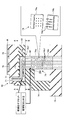
- the longitudinal section which shows an example of the heater electric power feeding mechanism containing electric power feeding assembly As1 concerning one embodiment.
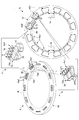
- “A” in FIG. 3 is an upper surface of the holding plate according to the embodiment
- “b” in FIG. 3 is a lower surface of the holding plate according to the embodiment
- “c” and “d” in FIG. The figure which shows electric power feeding assembly As1, As2 of the heater electric power feeding mechanism which concerns on a form.
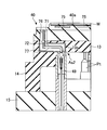
- the longitudinal section which shows an example of the heater electric power feeding mechanism containing electric power feeding assembly As2 concerning one embodiment.
- FIG. 1 shows a longitudinal section of a semiconductor manufacturing apparatus 1 according to an embodiment of the present invention.
- a capacitively coupled plasma etching apparatus is taken as an example of the semiconductor manufacturing apparatus 1.
- the semiconductor manufacturing apparatus 1 has a cylindrical chamber 10 made of aluminum whose surface is anodized (anodized), for example.
- the chamber 10 is grounded.
- a stage 12 is provided inside the chamber 10.
- the stage 12 has an electrostatic chuck (ESC) 40.
- the electrostatic chuck 40 is held by the holding plate 13.
- the electrostatic chuck 40 includes an electrode 40a made of a conductive film and an insulating layer 40b (or an insulating sheet) sandwiching the electrode 40a.
- the DC voltage source 42 supplies current to the electrode 40 a through the feeder line 49 in accordance with the control of the switch 43.
- the electrostatic chuck 40 generates a coulomb force by the current supplied from the DC voltage source 42 to attract and hold the semiconductor wafer (hereinafter referred to as “wafer W”) on the electrostatic chuck.
- heater 75 In the electrostatic chuck 40, heaters 75a, 75b, 75c, and 75d (hereinafter collectively referred to as “heater 75”) are embedded.
- the heater 75 may be attached to the back surface of the electrostatic chuck 40 instead of being embedded in the electrostatic chuck 40.
- the heater 75 is connected to the heater power supply mechanism 100 and is connected to the AC power supply 44 via the power supply line 47.
- the current output from the AC power supply 44 is supplied to the heaters 75a, 75b, 75c, and 75d through the power supply line 47 and the heater power supply mechanism 100, respectively.
- the heater power supply mechanism 100 can perform multi-zone control in which the stage 12 is divided into a plurality of zones using a plurality of heaters 75 and the temperature of the stage 12 is controlled for each zone.
- a focus ring 18 made of, for example, silicon or quartz is disposed on the periphery of the electrostatic chuck 40 in order to improve the in-plane uniformity of etching.
- a refrigerant pipe is formed inside the stage 12.
- the refrigerant supplied from the chiller unit circulates through the refrigerant pipe and the heater 75 is heated, so that the temperature of each zone of the electrostatic chuck 40 is independently controlled, whereby the wafer W is adjusted to a desired temperature.
- the heater power supply mechanism 100 includes a plurality of heater terminals 71, a plurality of heater wires 72, and an offset structure 73 that offsets the plurality of heater wires 72.
- offset in the present embodiment means that the heater wires 72 are arranged at desired positions while the heater wires 72 are shifted.
- the plurality of heater terminals 71 are connected to the plurality of heaters 75.
- the plurality of heater terminals 71 are arranged on the outer peripheral portion on the holding plate 13 that holds the stage 12.
- the plurality of heater wires 72 are connected to the AC power supply 44 through the power supply line 47.
- the holding plate 13 is made of an insulating member.
- the holding plate 13 may be made of a metal such as aluminum (Al), titanium (Ti), silicon carbide (SiC), or the like.
- the holding plate 13 is supported by an insulating support portion 14 and a base plate 15. Thereby, the stage 12 is fixed to the bottom of the chamber 10.
- An exhaust pipe 26 that forms an exhaust port 24 is provided at the bottom of the chamber 10, and the exhaust pipe 26 is connected to an exhaust device 28.
- the exhaust device 28 is composed of a vacuum pump such as a turbo molecular pump or a dry pump.
- the exhaust device 28 depressurizes the processing space in the chamber 10 to a predetermined vacuum level, and guides the gas in the chamber 10 to the exhaust path 20 and the exhaust port 24.
- a baffle plate 22 for controlling the gas flow is attached to the exhaust path 20.
- a first high-frequency power source 31 for exciting plasma is connected to the stage 12 via a matching unit 33, and a second high-frequency power source 32 for drawing ions in the plasma to the wafer W is connected via a matching unit 34.
- the first high frequency power supply 31 applies a high frequency power of a frequency suitable for generating plasma in the chamber 10, for example, 60 MHz, to the stage 12.
- the second high-frequency power source 32 has a lower frequency than the high-frequency power output from the first high-frequency power source 31, for example 0.8 MHz, suitable for drawing ions in the plasma into the wafer W on the stage 12. Apply to stage 12. In this way, the stage 12 functions as a lower electrode while placing the wafer W thereon.
- the shower head 38 is provided on the ceiling of the chamber 10 as an upper electrode having a ground potential. As a result, high frequency power from the first high frequency power supply 31 is capacitively applied between the stage 12 and the shower head 38.
- the shower head 38 includes an electrode plate 56 having a large number of gas vent holes 56a, and an electrode support 58 that detachably supports the electrode plate 56.
- the gas supply source 62 supplies gas into the shower head 38 from the gas inlet 60 a via the gas supply pipe 64.
- the gas is introduced into the chamber 10 through a number of gas vents 56a.
- a magnet 66 extending annularly or concentrically is disposed around the chamber 10 to control plasma generated in a plasma generation space between the upper electrode and the lower electrode by a magnetic force.
- the control unit 48 includes a CPU, a ROM (Read Only Memory), and a RAM (Random Access Memory), and controls the temperature of the etching and the electrostatic chuck 40 according to a procedure set in a recipe stored in the RAM or the like. Note that the function of the control unit 48 may be realized using software, or may be realized using hardware.
- the wafer W is carried into the chamber 10 from the opened gate valve 30 while being held on the transfer arm.
- the wafer W is held by pusher pins above the electrostatic chuck 40, and is placed on the electrostatic chuck 40 when the pusher pins descend.
- the gate valve 30 is closed after the wafer W is loaded.
- the pressure in the chamber 10 is reduced to a set value by the exhaust device 28.
- Gas is introduced into the chamber 10 from the shower head 38 in the form of a shower.
- the introduced gas is ionized and dissociated by high-frequency power, and plasma is generated.
- Plasma processing such as plasma etching is performed on the wafer W by the action of plasma. After the plasma etching is completed, the wafer W is held on the transfer arm and carried out of the chamber 10. By repeating the above processing for a plurality of wafers W, continuous processing of the wafers W is executed.
- the five heaters 75 are embedded in the electrostatic chuck 40.
- the present invention is not limited to this, and the heaters 75 may be provided on any of the stages 12. Further, the number of heaters 75 may be any number as long as it is two or more.
- the heater power supply mechanism 100 As the number of divided heaters 75 increases, the heater wiring increases, which interferes with other members provided in the semiconductor manufacturing apparatus 1, and troubles are likely to occur during assembly and maintenance of the semiconductor manufacturing apparatus 1. Work efficiency at the time becomes worse. Therefore, in the present embodiment, even if the number of heaters 75 is increased, the heater power supply is performed so as not to interfere with other members provided in the semiconductor manufacturing apparatus 1, avoid problems during assembly and maintenance, and improve work efficiency. It has a mechanism 100.
- the heater power supply mechanism 100 will be described in detail with reference to FIGS. 2 and 3.
- FIG. 2 shows an example of a longitudinal section of the heater power supply mechanism 100 according to the present embodiment.
- “A” in FIG. 3 shows the upper surface of the holding plate 13 according to the present embodiment.
- “B” in FIG. 3 shows the lower surface of the holding plate 13 according to the present embodiment.
- “C” in FIG. 3 indicates the power supply assembly As1 included in the heater power supply mechanism 100 according to the present embodiment, and “d” in FIG. 3 indicates the power supply assembly As2.
- the heater power supply mechanism 100 includes a plurality of heater terminals 71, a plurality of heater wires 72 connected to the plurality of heater terminals 71, and a plurality of heater wires 72. And an offset structure 73 for offsetting them as a set.
- “A” in FIG. 3 is the AA plane in FIG. 2 and shows the upper surface of the holding plate 13. According to this, a plurality of terminals are grouped, and a terminal group including a number of heater terminals 71 and electrode terminals 76 necessary for temperature control is arranged on the outer peripheral portion of the holding plate 13.
- the outer peripheral portion on the holding plate 13 where the terminal group is arranged corresponds to a region where the wafer W on the stage 12 is not placed.
- the power feeding position of the heater 75 and the power feeding position of the electrode of the electrostatic chuck 40 are arranged outside the line where the heater wiring 72 and the like go. Therefore, in the present embodiment, the power supply line such as the heater wiring 72 is not directly below the position of each power supply terminal, but is shifted from the position of each power supply terminal.
- the heater terminal 71 and the electrode terminal 76 are arranged outside the surface on which the wafer W is placed on the electrostatic chuck 40.
- the offset structure 73 arranges each heater wiring 72 at a desired position while shifting the heater wiring 72 (offset).
- the heater wiring 72 is connected to a heater terminal 71 that is a plurality of heater wires.
- the offset heater wires 72 are collected by a collecting unit 80 (see “b” in FIGS. 2 and 3) provided in the lower part of the holding plate 13.
- the consolidating unit 80 is a resin case for consolidating the heater wiring of each offset structure 73 and connecting it to the connector.
- the heater wiring group collected by the aggregation unit 80 is connected to the connector 74.
- the connector 74 is connected to the power supply line 47.
- the upper part 74 a of the connector 74 is connected to the heater wiring group.
- each terminal 74 b 1 provided on the lower part 74 b of the connector 74 is connected to the connector 74. It is inserted into the upper part 74a. As a result, the connection can be performed simultaneously with the attachment / detachment of the electrostatic chuck 40.
- the number of connectors 74 may be any number as long as one or more connectors 74 are provided. Further, the connector 74 is not limited to the position indicated by “b” in FIG. 3, and may be disposed at any position around the aggregation unit 80.
- the heater power supply mechanism 100 includes two types of power supply assemblies (hereinafter collectively referred to as “power supply assembly As”), as illustrated in a power supply assembly As1 of “c” in FIG. 3 and a power supply assembly As2 of “d” in FIG. .)
- the power supply assembly As ⁇ b> 1 is an assembly including a plurality of heater terminals 71, a plurality of heater wires 72, and an offset structure 73 as a unit.
- the plurality of heater terminals 71 are connected to a plurality of heater wires 72, respectively.
- the plurality of heater wires 72 are offset inside the case 73a.
- the case 73a may be made of resin, for example.
- a plurality of heater terminals 71 protrude from the upper portion of the case 73a.
- the plurality of heater wires 72 are wired in an offset manner inside the case 73a (offset), and output from a desired position at the bottom of the case 73a to the outside.
- the heater wiring 72 is connected to the power supply line 47 via the consolidating unit 80 and the connector 74. As a result, the current from the AC power supply 44 is supplied to the heater 75 from the heater terminal 71 via the power supply line 47, the connector 74 and the heater wiring 72.
- the power feeding assembly As2 includes one electrode terminal 76, a number of heater terminals 71 excluding the electrode terminal 76, one DC current wiring 77, and a heater terminal 71.
- the assembly includes a plurality of heater wires 72 and offset structures 73 connected to each other.
- the electrode terminal 76 is connected to a direct current wiring 77.
- the wirings 72 and 77 are offset inside the case 73b.
- the case 73b may be made of resin, for example.
- a number of heater terminals 71 excluding one electrode terminal 76 and the electrode terminals protrude from the upper part of the case 73b.
- One DC current wiring 77 and a plurality of heater wirings 72 are shifted inside the case 73b (offset) and output to the outside from a desired position at the bottom of the case 73b.
- the direct current wiring 77 is connected to the feeder line 49 via the consolidating unit 80.
- the current from the DC voltage source 42 is supplied to the electrode terminal 76 via the power supply line 49 and the DC current wiring 77.
- the plurality of heater wires 72 are connected to the power supply line 47 via the aggregation unit 80 and the connector 74.
- “B” in FIG. 3 is the BB surface in FIG. 2 and shows the lower surface of the holding plate 13.
- eleven power supply assemblies As1 and one power supply assembly As2 are assembled and fixed in the holding plate 13 by welding or the like. Accordingly, the power feeding assemblies As1 and As2 are stored in predetermined positions in the holding plate 13.
- the direct current wiring 77 connected to 76 is exposed from each case and is collected in the consolidating portion 80 under the holding plate 13.
- the aggregation portion 80 is formed in a substantially annular shape, and each wiring is aggregated in a resin case and is brought up to the connector 74 to be connected to the connector 74.
- FIGS. 2 and 4 there is a space between the holding plate 13 and the base plate 15.
- members for example, shown as a member Pt in FIG. 4
- pusher pins and thermometers that hold the wafer W up and down during loading and unloading are stored.
- the heater wiring 72 and the direct current wiring 77 are offset for each of the power supply assemblies As1 and As2. Further, the offset heater wiring 72 and the DC current wiring 77 are aggregated by the aggregation unit 80 and connected to the connector 74 or the like.
- the power supply assemblies As1 and As2 can be attached to predetermined positions of the holding plate 13 from below with the power supply assemblies As1 and As2 assembled in advance.
- the assembly process of the heater power supply mechanism 100 can be shortened, and the heater wiring 72 and the direct current wiring 77 can be easily connected in a short time.
- the work efficiency at the time of the assembly of a heater electric power feeding mechanism or a maintenance can be improved.
- the heater terminal 71 and the electrode terminal 76 are arranged outside the surface on which the wafer W on the electrostatic chuck 40 is placed. Thereby, the Joule heat from the heater terminal 71 and the electrode terminal 76 can be prevented from affecting the wafer W, and the in-plane uniformity of the wafer W temperature can be improved. In particular, even when the number of heater terminals 71 is increased by the multi-zone control of the electrostatic chuck 40 temperature, the in-plane uniformity of the wafer W temperature can be maintained.
- the heater power supply mechanism was demonstrated by the said embodiment, the heater power supply mechanism concerning this invention is not limited to the said embodiment, A various deformation
- the heater power supply mechanism 100 performs temperature control by dividing the electrostatic chuck 40 into a plurality of zones for each heater.
- the heater power supply mechanism according to the present invention is not limited to this, and a plurality of heaters are embedded in a member (for example, the holding plate 13) other than the electrostatic chuck 40, and the heater plate is divided into a plurality of zones for each heater.
- the 13 temperatures may be multi-zone controlled.
- the power supply assemblies As1 and As2 of the heater power supply mechanism 100 according to the present invention have a plurality of heater terminals 71, a plurality of heater wires 72, and an offset structure 73 that offsets the plurality of heater wires 72. did.
- the number of the power feeding assemblies of the two types of heater power feeding mechanisms according to the present invention and the number of each part constituting the power feeding assembly are not limited to the number of the present embodiment.
- the heater power feeding mechanism according to the present invention is a capacitively coupled type.
- the present invention can be applied not only to a plasma (CCP: Capacitively Coupled Plasma) apparatus but also to other semiconductor manufacturing apparatuses.
- CCP Capacitively Coupled Plasma
- ICP inductively coupled plasma
- CVD Chemical Vapor Deposition
- HWP Helicon Wave Plasma
- ECR cyclotron resonance plasma
- the substrate processed by the semiconductor manufacturing apparatus using the heater power supply mechanism according to the present invention is not limited to a wafer.
- a large substrate for a flat panel display, an EL element, or a solar cell It may be a substrate.
Landscapes
- Engineering & Computer Science (AREA)
- Manufacturing & Machinery (AREA)
- Chemical & Material Sciences (AREA)
- Ceramic Engineering (AREA)
- Inorganic Chemistry (AREA)
- Container, Conveyance, Adherence, Positioning, Of Wafer (AREA)
- Drying Of Semiconductors (AREA)
- Physics & Mathematics (AREA)
- Plasma & Fusion (AREA)
- Resistance Heating (AREA)
- Control Of Resistance Heating (AREA)
Abstract
Description
基板を載置するステージを複数のヒータを用いて複数のゾーンに分け、ゾーン毎に温度制御可能なヒータ給電機構であって、
前記複数のヒータに接続される複数のヒータ用端子と、
前記複数のヒータ用端子に接続される複数のヒータ配線と、
前記複数のヒータ配線をオフセットするオフセット構造と、を有し、
前記複数のヒータ用端子は、前記ステージを保持する保持プレート上の外周部に配置される、ヒータ給電機構が提供される。
まず、本発明の一実施形態に係る半導体製造装置1の全体構成について、図1を参照しながら説明する。図1は、本発明の一実施形態に係る半導体製造装置1の縦断面を示す。本実施形態では、半導体製造装置1の一例として容量結合型プラズマエッチング装置を挙げる。
図2は、本実施形態に係るヒータ給電機構100の縦断面の一例を示す。図3の「a」は、本実施形態に係る保持プレート13の上面を示す。図3の「b」は、本実施形態に係る保持プレート13の下面を示す。図3の「c」は、本実施形態に係るヒータ給電機構100が有する給電アセンブリAs1,図3の「d」は、給電アセンブリAs2を示す。
ヒータ給電機構100は、図3の「c」の給電アセンブリAs1及び図3の「d」の給電アセンブリAs2に示すように、2種類の給電アセンブリ(以下、総称して「給電アセンブリAs」ともいう。)を有する。図3の「c」に示すように、給電アセンブリAs1は、複数個のヒータ用端子71、複数本のヒータ配線72及びオフセット構造73を一単位としたアセンブリである。複数個のヒータ用端子71は、複数本のヒータ配線72とそれぞれ接続されている。複数本のヒータ配線72は、ケース73aの内部でオフセットされる。ケース73aは、例えば、樹脂で構成されてもよい。
また、本発明に係るヒータ給電機構は、容量結合型プラズマ(CCP:Capacitively Coupled Plasma)装置だけでなく、その他の半導体製造装置に適用可能である。その他の半導体製造装置としては、誘導結合型プラズマ(ICP:Inductively Coupled Plasma)、ラジアルラインスロットアンテナを用いたCVD(Chemical Vapor Deposition)装置、ヘリコン波励起型プラズマ(HWP:Helicon Wave Plasma)装置、電子サイクロトロン共鳴プラズマ(ECR:Electron Cyclotron Resonance Plasma)装置等であってもよい。
10:チャンバ
12:ステージ(下部電極)
13:保持プレート
28:排気装置
38:シャワーヘッド(上部電極)
40:静電チャック
44:交流電源
42:直流電圧源
47,49:給電線
71:ヒータ用端子
72:ヒータ配線
73:オフセット構造
73a:ケース
73b:ケース
74:コネクタ
76:電極用端子
77:直流電流用の配線
80:集約部
100:ヒータ給電機構
As1、As2:給電アセンブリ
Claims (7)
- 基板を載置するステージを複数のヒータを用いて複数のゾーンに分け、ゾーン毎に温度制御可能なヒータ給電機構であって、
前記複数のヒータに接続される複数のヒータ用端子と、
前記複数のヒータ用端子に接続される複数のヒータ配線と、
前記複数のヒータ配線をオフセットするオフセット構造と、を有し、
前記複数のヒータ用端子は、前記ステージを保持する保持プレート上の外周部に配置される、ヒータ給電機構。 - 前記オフセット構造にてオフセットされた複数のヒータ配線を纏める集約部と、
前記集約部で纏められた前記複数のヒータ配線と接続されるコネクタと、
を有する請求項1に記載のヒータ給電機構。 - 前記オフセット構造は、所定個数のヒータ用端子及び所定本のヒータ配線を一単位としたアセンブリとして組み立てられた状態で前記保持プレートに装着される、
請求項1に記載のヒータ給電機構。 - 前記オフセット構造は、電極用端子とヒータ用端子とを含む所定個数の端子、及び直流電流用の配線とヒータ配線とを含む所定本の配線を一単位としたアセンブリとして組み立てられた状態で前記保持プレートに装着される、
請求項1に記載のヒータ給電機構。 - 前記ステージは、静電チャックを有し、前記複数のヒータは、前記静電チャックに設けられる、
請求項1に記載のヒータ給電機構。 - 前記複数のヒータ用端子が配置される前記保持プレート上の外周部は、前記ステージ上の基板が載置されない領域に対応する、
請求項1に記載のヒータ給電機構。 - 前記保持プレートは、絶縁性部材により構成される、
請求項1に記載のヒータ給電機構。
Priority Applications (5)
| Application Number | Priority Date | Filing Date | Title |
|---|---|---|---|
| US15/300,349 US20170140958A1 (en) | 2014-05-19 | 2015-05-08 | Heater power feeding mechanism |
| KR1020217037732A KR102400032B1 (ko) | 2014-05-19 | 2015-05-08 | 히터 급전 기구 |
| CN201580020523.5A CN106233435B (zh) | 2014-05-19 | 2015-05-08 | 加热器供电机构 |
| KR1020167029093A KR102330245B1 (ko) | 2014-05-19 | 2015-05-08 | 히터 급전 기구 |
| US17/399,055 US11756806B2 (en) | 2014-05-19 | 2021-08-11 | Heater power feeding mechanism |
Applications Claiming Priority (2)
| Application Number | Priority Date | Filing Date | Title |
|---|---|---|---|
| JP2014-103511 | 2014-05-19 | ||
| JP2014103511A JP6219229B2 (ja) | 2014-05-19 | 2014-05-19 | ヒータ給電機構 |
Related Child Applications (2)
| Application Number | Title | Priority Date | Filing Date |
|---|---|---|---|
| US15/300,349 A-371-Of-International US20170140958A1 (en) | 2014-05-19 | 2015-05-08 | Heater power feeding mechanism |
| US17/399,055 Continuation US11756806B2 (en) | 2014-05-19 | 2021-08-11 | Heater power feeding mechanism |
Publications (1)
| Publication Number | Publication Date |
|---|---|
| WO2015178222A1 true WO2015178222A1 (ja) | 2015-11-26 |
Family
ID=54553895
Family Applications (1)
| Application Number | Title | Priority Date | Filing Date |
|---|---|---|---|
| PCT/JP2015/063286 Ceased WO2015178222A1 (ja) | 2014-05-19 | 2015-05-08 | ヒータ給電機構 |
Country Status (6)
| Country | Link |
|---|---|
| US (2) | US20170140958A1 (ja) |
| JP (1) | JP6219229B2 (ja) |
| KR (2) | KR102330245B1 (ja) |
| CN (1) | CN106233435B (ja) |
| TW (1) | TWI646614B (ja) |
| WO (1) | WO2015178222A1 (ja) |
Cited By (1)
| Publication number | Priority date | Publication date | Assignee | Title |
|---|---|---|---|---|
| JP2022133380A (ja) * | 2017-12-15 | 2022-09-13 | ラム リサーチ コーポレーション | プラズマチャンバ内で使用するためのリング構造およびシステム |
Families Citing this family (18)
| Publication number | Priority date | Publication date | Assignee | Title |
|---|---|---|---|---|
| US10388493B2 (en) * | 2011-09-16 | 2019-08-20 | Lam Research Corporation | Component of a substrate support assembly producing localized magnetic fields |
| JP5973731B2 (ja) * | 2012-01-13 | 2016-08-23 | 東京エレクトロン株式会社 | プラズマ処理装置及びヒータの温度制御方法 |
| JP6608444B2 (ja) * | 2015-12-28 | 2019-11-20 | 日本碍子株式会社 | 円板状ヒータ及びヒータ冷却板アセンブリ |
| JP6674800B2 (ja) | 2016-03-07 | 2020-04-01 | 日本特殊陶業株式会社 | 基板支持装置 |
| US10764966B2 (en) * | 2016-05-10 | 2020-09-01 | Lam Research Corporation | Laminated heater with different heater trace materials |
| JP6698502B2 (ja) * | 2016-11-21 | 2020-05-27 | 東京エレクトロン株式会社 | 載置台及びプラズマ処理装置 |
| CN108281342B (zh) * | 2017-01-05 | 2020-01-21 | 东京毅力科创株式会社 | 等离子体处理装置 |
| JP6865128B2 (ja) * | 2017-07-19 | 2021-04-28 | 東京エレクトロン株式会社 | プラズマ処理装置 |
| US11837446B2 (en) * | 2017-07-31 | 2023-12-05 | Lam Research Corporation | High power cable for heated components in RF environment |
| JP6866255B2 (ja) * | 2017-08-09 | 2021-04-28 | 東京エレクトロン株式会社 | プラズマ処理装置 |
| JP6760242B2 (ja) * | 2017-10-13 | 2020-09-23 | 住友電気工業株式会社 | ヒータモジュール |
| JP7033441B2 (ja) * | 2017-12-01 | 2022-03-10 | 東京エレクトロン株式会社 | プラズマ処理装置 |
| JP7208819B2 (ja) * | 2018-03-26 | 2023-01-19 | 東京エレクトロン株式会社 | プラズマ処理装置 |
| CN109175587B (zh) * | 2018-08-03 | 2021-01-26 | 东莞市众兴电子科技有限公司 | 一种dc线焊接机 |
| US11488808B2 (en) * | 2018-11-30 | 2022-11-01 | Tokyo Electron Limited | Plasma processing apparatus, calculation method, and calculation program |
| JP7300310B2 (ja) * | 2019-05-20 | 2023-06-29 | 東京エレクトロン株式会社 | 載置台の温度調整方法、検査装置及び載置台 |
| US11651986B2 (en) | 2021-01-27 | 2023-05-16 | Applied Materials, Inc. | System for isolating electrodes at cryogenic temperatures |
| KR102716890B1 (ko) | 2022-03-29 | 2024-10-16 | 토토 가부시키가이샤 | 정전 척 |
Citations (3)
| Publication number | Priority date | Publication date | Assignee | Title |
|---|---|---|---|---|
| JP2001057370A (ja) * | 1999-03-04 | 2001-02-27 | Applied Materials Inc | 基板支持台内部の温度勾配を減少させる方法及び装置 |
| US20020185487A1 (en) * | 2001-05-02 | 2002-12-12 | Ramesh Divakar | Ceramic heater with heater element and method for use thereof |
| JP2003146770A (ja) * | 2001-07-09 | 2003-05-21 | Ibiden Co Ltd | セラミック接合体 |
Family Cites Families (144)
| Publication number | Priority date | Publication date | Assignee | Title |
|---|---|---|---|---|
| US1348648A (en) * | 1916-10-23 | 1920-08-03 | Sherman L Kelly | Electric heating element and wiring therefor |
| US1417154A (en) * | 1920-07-15 | 1922-05-23 | Steatite Electric Products Cor | Electric heating apparatus |
| US1534673A (en) * | 1923-01-10 | 1925-04-21 | William W Weir | Electrical heating element |
| US2494447A (en) * | 1947-04-29 | 1950-01-10 | Steatite Res Corp | Heating grill |
| US3500018A (en) * | 1966-08-01 | 1970-03-10 | Teledyne Inc | Electric heater apparatus |
| US3740513A (en) * | 1971-09-23 | 1973-06-19 | Environment One Corp | Improved consumer oriented combined counter and cooking unit using induction heating |
| JPS577082A (en) * | 1980-06-13 | 1982-01-14 | Riccar Sewing Machine Kk | Exciter for induction heater |
| EP0103741B1 (de) * | 1982-09-16 | 1988-11-17 | E.G.O. Elektro-Geräte Blanc u. Fischer | Heizelement, insbesondere Strahlungsheizelement für die Beheizung von Glaskeramikplatten |
| DE3315438A1 (de) * | 1983-04-28 | 1984-10-31 | E.G.O. Elektro-Geräte Blanc u. Fischer, 7519 Oberderdingen | Heizelement zur beheizung von koch-, heizplatten oder dgl. |
| US4629843A (en) * | 1984-04-11 | 1986-12-16 | Tdk Corporation | Induction cooking apparatus having a ferrite coil support |
| DE3519350A1 (de) * | 1985-05-30 | 1986-12-04 | E.G.O. Elektro-Geräte Blanc u. Fischer, 7519 Oberderdingen | Strahlungs-heizeinheit |
| DE8711209U1 (de) * | 1987-08-18 | 1987-10-01 | E.G.O. Elektro-Geräte Blanc u. Fischer, 7519 Oberderdingen | Elektrischer Heizkörper |
| US4993553A (en) * | 1988-02-09 | 1991-02-19 | E.G.O. Elektro Gerate Blanc U. Fischer | Electric hotplate stacking aid |
| US4961798A (en) * | 1989-10-02 | 1990-10-09 | Commercial Resins Company | Sleeve applicator assembly for pipe joints |
| DE4022292A1 (de) * | 1990-07-15 | 1992-01-16 | Ego Elektro Blanc & Fischer | Elektrisches strahlungsheizelement |
| DE69130205T2 (de) * | 1990-12-25 | 1999-03-25 | Ngk Insulators, Ltd., Nagoya, Aichi | Heizungsapparat für eine Halbleiterscheibe und Verfahren zum Herstellen desselben |
| EP1120817B8 (en) * | 1991-03-26 | 2007-10-10 | Ngk Insulators, Ltd. | Use of a corrosion-resistant member |
| US5796075A (en) * | 1992-03-09 | 1998-08-18 | E.G.O. Elektro-Gerate Blanc Und Fisher Gmbh & Co. Kg | Heater, particularly for kitchen appliances |
| DE4229375C2 (de) * | 1992-09-03 | 2000-05-04 | Ego Elektro Blanc & Fischer | Strahlungs-Heizkörper |
| KR0126736Y1 (ko) * | 1992-07-09 | 1998-12-15 | 강진구 | 삶는 세탁기의 히터안전장치 |
| US5800618A (en) * | 1992-11-12 | 1998-09-01 | Ngk Insulators, Ltd. | Plasma-generating electrode device, an electrode-embedded article, and a method of manufacturing thereof |
| JP2647799B2 (ja) * | 1994-02-04 | 1997-08-27 | 日本碍子株式会社 | セラミックスヒーター及びその製造方法 |
| JP2754163B2 (ja) * | 1994-05-31 | 1998-05-20 | 信越半導体株式会社 | 高周波誘導加熱コイル |
| FR2723248B1 (fr) * | 1994-07-29 | 1996-09-20 | Seb Sa | Procede de realisation d'un inducteur |
| US6133557A (en) * | 1995-01-31 | 2000-10-17 | Kyocera Corporation | Wafer holding member |
| DE19518109A1 (de) * | 1995-05-17 | 1996-11-21 | Ego Elektro Blanc & Fischer | Strahlungs-Heizer |
| US5603858A (en) * | 1995-06-02 | 1997-02-18 | Aladdin Synergetics, Inc. | Heat retentive server for induction heating |
| JP3599204B2 (ja) * | 1995-06-08 | 2004-12-08 | アネルバ株式会社 | Cvd装置 |
| EP0992470B1 (en) * | 1995-08-03 | 2006-03-08 | Ngk Insulators, Ltd. | Aluminium nitride sintered bodies and their use as substrate in an apparatus for producing semiconductors |
| JP3457477B2 (ja) * | 1995-09-06 | 2003-10-20 | 日本碍子株式会社 | 静電チャック |
| JP3670416B2 (ja) * | 1995-11-01 | 2005-07-13 | 日本碍子株式会社 | 金属包含材および静電チャック |
| US6036878A (en) * | 1996-02-02 | 2000-03-14 | Applied Materials, Inc. | Low density high frequency process for a parallel-plate electrode plasma reactor having an inductive antenna |
| DE19603845B4 (de) * | 1996-02-05 | 2010-07-22 | E.G.O. Elektro-Gerätebau GmbH | Elektrischer Strahlungsheizkörper mit einem aktiven Sensor zur Kochgefäßerkennung |
| KR100280634B1 (ko) * | 1996-05-05 | 2001-02-01 | 세이이치로 미야타 | 전기 발열체 및 이를 이용한 정전 척 |
| US5954984A (en) * | 1996-07-31 | 1999-09-21 | Thermal Solutions Inc. | Heat retentive food servingware with temperature self-regulating phase change core |
| JP3316167B2 (ja) * | 1996-10-08 | 2002-08-19 | 日本碍子株式会社 | 窒化アルミニウム質基材の接合体の製造方法およびこれに使用する接合助剤 |
| US5886864A (en) * | 1996-12-02 | 1999-03-23 | Applied Materials, Inc. | Substrate support member for uniform heating of a substrate |
| JP3604888B2 (ja) * | 1997-01-30 | 2004-12-22 | 日本碍子株式会社 | 窒化アルミニウム質セラミックス基材の接合体、窒化アルミニウム質セラミックス基材の接合体の製造方法及び接合剤 |
| EP1029426B1 (en) * | 1997-03-13 | 2005-02-16 | Aktiebolaget Electrolux | A table top with induction heating elements |
| JPH11260534A (ja) * | 1998-01-09 | 1999-09-24 | Ngk Insulators Ltd | 加熱装置およびその製造方法 |
| US6273022B1 (en) * | 1998-03-14 | 2001-08-14 | Applied Materials, Inc. | Distributed inductively-coupled plasma source |
| US6316753B2 (en) * | 1998-05-19 | 2001-11-13 | Thermal Solutions, Inc. | Induction heating, temperature self-regulating |
| JP4641569B2 (ja) * | 1998-07-24 | 2011-03-02 | 日本碍子株式会社 | 窒化アルミニウム質焼結体、耐蝕性部材、金属埋設および半導体保持装置 |
| JP3983387B2 (ja) * | 1998-09-29 | 2007-09-26 | 日本碍子株式会社 | 静電チャック |
| WO2001011921A1 (en) * | 1999-08-09 | 2001-02-15 | Ibiden Co., Ltd. | Ceramic heater |
| JP2001056346A (ja) * | 1999-08-19 | 2001-02-27 | Fujitsu Ltd | プローブカード及び複数の半導体装置が形成されたウエハの試験方法 |
| US6488820B1 (en) * | 1999-08-23 | 2002-12-03 | Applied Materials, Inc. | Method and apparatus for reducing migration of conductive material on a component |
| US6740853B1 (en) * | 1999-09-29 | 2004-05-25 | Tokyo Electron Limited | Multi-zone resistance heater |
| WO2001041508A1 (en) * | 1999-11-30 | 2001-06-07 | Ibiden Co., Ltd. | Ceramic heater |
| JP4209057B2 (ja) * | 1999-12-01 | 2009-01-14 | 東京エレクトロン株式会社 | セラミックスヒーターならびにそれを用いた基板処理装置および基板処理方法 |
| US6255633B1 (en) * | 1999-12-28 | 2001-07-03 | Toshiba Tec Kabushiki Kaisha | Fixing device using induction heating |
| JP3567855B2 (ja) * | 2000-01-20 | 2004-09-22 | 住友電気工業株式会社 | 半導体製造装置用ウェハ保持体 |
| US6891263B2 (en) * | 2000-02-07 | 2005-05-10 | Ibiden Co., Ltd. | Ceramic substrate for a semiconductor production/inspection device |
| US6861165B2 (en) * | 2000-02-24 | 2005-03-01 | Ibiden Co., Ltd. | Aluminum nitride sintered compact, ceramic substrate, ceramic heater and electrostatic chuck |
| US6534751B2 (en) * | 2000-02-28 | 2003-03-18 | Kyocera Corporation | Wafer heating apparatus and ceramic heater, and method for producing the same |
| JP3492325B2 (ja) * | 2000-03-06 | 2004-02-03 | キヤノン株式会社 | 画像表示装置の製造方法 |
| JP2001247382A (ja) * | 2000-03-06 | 2001-09-11 | Ibiden Co Ltd | セラミック基板 |
| US20030098299A1 (en) * | 2000-03-06 | 2003-05-29 | Ibiden Co., Ltd. | Ceramic heater |
| WO2001066488A1 (en) * | 2000-03-07 | 2001-09-13 | Ibiden Co., Ltd. | Ceramic substrate for manufacture/inspection of semiconductor |
| JP2001253777A (ja) * | 2000-03-13 | 2001-09-18 | Ibiden Co Ltd | セラミック基板 |
| EP1383168A1 (en) * | 2000-03-15 | 2004-01-21 | Ibiden Co., Ltd. | Method of producing electrostatic chucks and method of producing ceramic heaters |
| EP1280380A1 (en) * | 2000-04-10 | 2003-01-29 | Ibiden Co., Ltd. | Ceramic board |
| JP2001302330A (ja) * | 2000-04-24 | 2001-10-31 | Ibiden Co Ltd | セラミック基板 |
| JP2002025758A (ja) * | 2000-05-02 | 2002-01-25 | Ibiden Co Ltd | ホットプレートユニット |
| EP1435654A3 (en) * | 2000-05-10 | 2004-07-14 | Ibiden Co., Ltd. | Electrostatic chuck |
| JP4398064B2 (ja) * | 2000-05-12 | 2010-01-13 | 日本発條株式会社 | 加熱装置 |
| WO2001091166A1 (en) * | 2000-05-26 | 2001-11-29 | Ibiden Co., Ltd. | Semiconductor manufacturing and inspecting device |
| JP3516392B2 (ja) * | 2000-06-16 | 2004-04-05 | イビデン株式会社 | 半導体製造・検査装置用ホットプレート |
| JP4672113B2 (ja) * | 2000-07-07 | 2011-04-20 | 東京エレクトロン株式会社 | 誘導結合プラズマ処理装置 |
| JP2002076102A (ja) * | 2000-08-31 | 2002-03-15 | Ibiden Co Ltd | セラミック基板 |
| JP2002160974A (ja) * | 2000-11-22 | 2002-06-04 | Ibiden Co Ltd | 窒化アルミニウム焼結体、窒化アルミニウム焼結体の製造方法、セラミック基板およびセラミック基板の製造方法 |
| US6960743B2 (en) * | 2000-12-05 | 2005-11-01 | Ibiden Co., Ltd. | Ceramic substrate for semiconductor manufacturing, and method of manufacturing the ceramic substrate |
| JP2002338388A (ja) * | 2001-02-15 | 2002-11-27 | Ngk Insulators Ltd | ダイヤモンドコート部材 |
| JPWO2002084717A1 (ja) * | 2001-04-11 | 2004-08-05 | イビデン株式会社 | 半導体製造・検査装置用セラミックヒータ |
| JP4294232B2 (ja) * | 2001-05-02 | 2009-07-08 | 日本特殊陶業株式会社 | セラミックヒータ及びそれを用いたグロープラグ |
| EP1406472A1 (en) * | 2001-07-09 | 2004-04-07 | Ibiden Co., Ltd. | Ceramic heater and ceramic joined article |
| WO2003015157A1 (en) * | 2001-08-10 | 2003-02-20 | Ibiden Co., Ltd. | Ceramic joint body |
| JP4745556B2 (ja) * | 2001-08-20 | 2011-08-10 | キヤノン株式会社 | 位置決め装置、露光装置、及びデバイス製造方法 |
| JP3886424B2 (ja) * | 2001-08-28 | 2007-02-28 | 鹿児島日本電気株式会社 | 基板処理装置及び方法 |
| JP4014912B2 (ja) * | 2001-09-28 | 2007-11-28 | 株式会社ルネサステクノロジ | 半導体装置 |
| CN1596557A (zh) * | 2001-11-30 | 2005-03-16 | 揖斐电株式会社 | 陶瓷加热器 |
| CN100508671C (zh) * | 2002-03-12 | 2009-07-01 | 松下电器产业株式会社 | 感应加热装置 |
| EP1492386B1 (en) * | 2002-03-19 | 2010-06-02 | Panasonic Corporation | Induction heating device |
| JP4026761B2 (ja) * | 2002-03-28 | 2007-12-26 | 日本碍子株式会社 | セラミックヒーター |
| JP2003300785A (ja) * | 2002-04-04 | 2003-10-21 | Ibiden Co Ltd | セラミック接合体およびセラミック接合体の製造方法 |
| JP2004055608A (ja) * | 2002-07-16 | 2004-02-19 | Sumitomo Osaka Cement Co Ltd | 電極内蔵型サセプタ |
| GB0217351D0 (en) * | 2002-07-25 | 2002-09-04 | Ceramaspeed Ltd | Radiant electric heater |
| JP4026759B2 (ja) * | 2002-11-18 | 2007-12-26 | 日本碍子株式会社 | 加熱装置 |
| JP2005026296A (ja) | 2003-06-30 | 2005-01-27 | Kowa Dennetsu Keiki:Kk | ホットプレ−トユニット |
| JP3748559B2 (ja) * | 2003-06-30 | 2006-02-22 | キヤノン株式会社 | ステージ装置、露光装置、荷電ビーム描画装置、デバイス製造方法、基板電位測定方法及び静電チャック |
| CN100438709C (zh) * | 2003-07-15 | 2008-11-26 | 松下电器产业株式会社 | 感应加热装置 |
| TWI247551B (en) * | 2003-08-12 | 2006-01-11 | Ngk Insulators Ltd | Method of manufacturing electrical resistance heating element |
| JP2005166354A (ja) * | 2003-12-01 | 2005-06-23 | Ngk Insulators Ltd | セラミックヒーター |
| DE102004003119A1 (de) * | 2004-01-21 | 2005-08-11 | BSH Bosch und Siemens Hausgeräte GmbH | Vorrichtung zum Erwärmen von Speisen mittels induktiver Kopplung und Vorrichtung zur Übertragung von Energie |
| JP4761723B2 (ja) * | 2004-04-12 | 2011-08-31 | 日本碍子株式会社 | 基板加熱装置 |
| DE502004005078D1 (de) * | 2004-04-30 | 2007-11-08 | Sgl Carbon Ag | Werkstückträger für die induktive Erwärmung von Werkstücken |
| KR100587681B1 (ko) * | 2004-05-07 | 2006-06-08 | 삼성전자주식회사 | 반도체 제조용 챔버의 히터블록 장착용 라인의 실링구조 |
| TW200612512A (en) * | 2004-06-28 | 2006-04-16 | Ngk Insulators Ltd | Substrate heating sapparatus |
| EP1811812B1 (en) * | 2005-02-04 | 2010-04-07 | Panasonic Corporation | Induction heater |
| US7776156B2 (en) * | 2005-02-10 | 2010-08-17 | Applied Materials, Inc. | Side RF coil and side heater for plasma processing apparatus |
| JP4707421B2 (ja) * | 2005-03-14 | 2011-06-22 | 東京エレクトロン株式会社 | 処理装置,処理装置の消耗部品管理方法,処理システム,処理システムの消耗部品管理方法 |
| US7535688B2 (en) * | 2005-03-25 | 2009-05-19 | Tokyo Electron Limited | Method for electrically discharging substrate, substrate processing apparatus and program |
| JP4787636B2 (ja) * | 2006-03-13 | 2011-10-05 | 東京エレクトロン株式会社 | 高圧処理装置 |
| US7848075B2 (en) * | 2006-07-19 | 2010-12-07 | Ngk Insulators, Ltd. | Electrostatic chuck with heater |
| US7901509B2 (en) * | 2006-09-19 | 2011-03-08 | Momentive Performance Materials Inc. | Heating apparatus with enhanced thermal uniformity and method for making thereof |
| US8573836B2 (en) * | 2006-10-26 | 2013-11-05 | Tokyo Electron Limited | Apparatus and method for evaluating a substrate mounting device |
| TW200836578A (en) * | 2006-11-27 | 2008-09-01 | Momentive Performance Mat Inc | Quartz encapsulated heater and heater assembly thereof |
| RU2449509C2 (ru) * | 2006-12-18 | 2012-04-27 | Панасоник Корпорэйшн | Устройство для приготовления пищи индукционным нагревом |
| DE112007003258B4 (de) * | 2007-01-15 | 2011-12-29 | Japan Unix Co. Ltd. | Laserlötvorrichtung |
| JP5203612B2 (ja) * | 2007-01-17 | 2013-06-05 | 株式会社日立ハイテクノロジーズ | プラズマ処理装置 |
| JP5042661B2 (ja) * | 2007-02-15 | 2012-10-03 | 東京エレクトロン株式会社 | プラズマ処理装置及びフィルタユニット |
| JP4838197B2 (ja) * | 2007-06-05 | 2011-12-14 | 東京エレクトロン株式会社 | プラズマ処理装置,電極温度調整装置,電極温度調整方法 |
| JP5161215B2 (ja) * | 2007-06-22 | 2013-03-13 | パナソニック株式会社 | 誘導加熱調理器 |
| JP5331407B2 (ja) * | 2007-08-17 | 2013-10-30 | 株式会社半導体エネルギー研究所 | 半導体装置の作製方法 |
| JP2009054871A (ja) * | 2007-08-28 | 2009-03-12 | Tokyo Electron Ltd | 載置台構造及び処理装置 |
| JP5301812B2 (ja) * | 2007-11-14 | 2013-09-25 | 東京エレクトロン株式会社 | プラズマ処理装置 |
| JP2009130229A (ja) * | 2007-11-27 | 2009-06-11 | Semiconductor Energy Lab Co Ltd | 半導体装置の作製方法 |
| JP2009152475A (ja) * | 2007-12-21 | 2009-07-09 | Shinko Electric Ind Co Ltd | 基板温調固定装置 |
| JP2009170509A (ja) * | 2008-01-11 | 2009-07-30 | Hitachi High-Technologies Corp | ヒータ内蔵静電チャックを備えたプラズマ処理装置 |
| JP5172367B2 (ja) * | 2008-01-23 | 2013-03-27 | 三菱電機株式会社 | 積層コア、積層コアの製造方法、積層コアの製造装置およびステータ |
| CN101938927A (zh) * | 2008-02-07 | 2011-01-05 | 三洋电机株式会社 | 电饭煲以及煮饭方法 |
| US8092637B2 (en) * | 2008-02-28 | 2012-01-10 | Hitachi High-Technologies Corporation | Manufacturing method in plasma processing apparatus |
| EP2281312A4 (en) * | 2008-04-04 | 2012-08-15 | Arthur R Zingher | DENSE MODULAR PHOTOVOLTAIC SOLAR RECEIVER FOR HIGH CONCENTRATION |
| US8853599B2 (en) * | 2008-05-27 | 2014-10-07 | Panasonic Corporation | Induction heating cooking apparatus |
| KR101006848B1 (ko) * | 2008-05-28 | 2011-01-14 | 주식회사 코미코 | 기판 지지 장치 및 이를 포함하는 기판 처리 장치 |
| US8206552B2 (en) * | 2008-06-25 | 2012-06-26 | Applied Materials, Inc. | RF power delivery system in a semiconductor apparatus |
| WO2010019430A2 (en) * | 2008-08-12 | 2010-02-18 | Applied Materials, Inc. | Electrostatic chuck assembly |
| JP5423205B2 (ja) * | 2008-08-29 | 2014-02-19 | 東京エレクトロン株式会社 | 成膜装置 |
| JP5342295B2 (ja) * | 2009-03-27 | 2013-11-13 | 東京エレクトロン株式会社 | ゲートバルブ装置 |
| JP5591573B2 (ja) * | 2009-03-30 | 2014-09-17 | 東京エレクトロン株式会社 | プラズマ処理装置及びプラズマ処理方法 |
| US8637794B2 (en) * | 2009-10-21 | 2014-01-28 | Lam Research Corporation | Heating plate with planar heating zones for semiconductor processing |
| WO2011048816A1 (ja) * | 2009-10-23 | 2011-04-28 | パナソニック株式会社 | 誘導加熱装置 |
| JP5592098B2 (ja) * | 2009-10-27 | 2014-09-17 | 東京エレクトロン株式会社 | プラズマ処理装置及びプラズマ処理方法 |
| JP5643062B2 (ja) * | 2009-11-24 | 2014-12-17 | 東京エレクトロン株式会社 | プラズマ処理装置 |
| US8598586B2 (en) * | 2009-12-21 | 2013-12-03 | Semiconductor Energy Laboratory Co., Ltd. | Thin film transistor and manufacturing method thereof |
| US8629370B2 (en) * | 2010-06-08 | 2014-01-14 | Applied Materials, Inc. | Assembly for delivering RF power and DC voltage to a plasma processing chamber |
| US8791392B2 (en) * | 2010-10-22 | 2014-07-29 | Lam Research Corporation | Methods of fault detection for multiplexed heater array |
| JP5203482B2 (ja) * | 2011-03-28 | 2013-06-05 | 株式会社小松製作所 | 加熱装置 |
| JP5384549B2 (ja) * | 2011-03-28 | 2014-01-08 | 株式会社小松製作所 | 加熱装置 |
| US9337067B2 (en) * | 2011-05-13 | 2016-05-10 | Novellus Systems, Inc. | High temperature electrostatic chuck with radial thermal chokes |
| US9307578B2 (en) * | 2011-08-17 | 2016-04-05 | Lam Research Corporation | System and method for monitoring temperatures of and controlling multiplexed heater array |
| US8809747B2 (en) * | 2012-04-13 | 2014-08-19 | Lam Research Corporation | Current peak spreading schemes for multiplexed heated array |
| JP5996340B2 (ja) * | 2012-09-07 | 2016-09-21 | 東京エレクトロン株式会社 | プラズマエッチング装置 |
| US10049948B2 (en) * | 2012-11-30 | 2018-08-14 | Lam Research Corporation | Power switching system for ESC with array of thermal control elements |
-
2014
- 2014-05-19 JP JP2014103511A patent/JP6219229B2/ja active Active
-
2015
- 2015-05-08 US US15/300,349 patent/US20170140958A1/en not_active Abandoned
- 2015-05-08 KR KR1020167029093A patent/KR102330245B1/ko active Active
- 2015-05-08 CN CN201580020523.5A patent/CN106233435B/zh active Active
- 2015-05-08 KR KR1020217037732A patent/KR102400032B1/ko active Active
- 2015-05-08 WO PCT/JP2015/063286 patent/WO2015178222A1/ja not_active Ceased
- 2015-05-15 TW TW104115486A patent/TWI646614B/zh active
-
2021
- 2021-08-11 US US17/399,055 patent/US11756806B2/en active Active
Patent Citations (3)
| Publication number | Priority date | Publication date | Assignee | Title |
|---|---|---|---|---|
| JP2001057370A (ja) * | 1999-03-04 | 2001-02-27 | Applied Materials Inc | 基板支持台内部の温度勾配を減少させる方法及び装置 |
| US20020185487A1 (en) * | 2001-05-02 | 2002-12-12 | Ramesh Divakar | Ceramic heater with heater element and method for use thereof |
| JP2003146770A (ja) * | 2001-07-09 | 2003-05-21 | Ibiden Co Ltd | セラミック接合体 |
Cited By (2)
| Publication number | Priority date | Publication date | Assignee | Title |
|---|---|---|---|---|
| JP2022133380A (ja) * | 2017-12-15 | 2022-09-13 | ラム リサーチ コーポレーション | プラズマチャンバ内で使用するためのリング構造およびシステム |
| JP7442582B2 (ja) | 2017-12-15 | 2024-03-04 | ラム リサーチ コーポレーション | プラズマチャンバ内で使用するためのリング構造およびシステム |
Also Published As
| Publication number | Publication date |
|---|---|
| US20210366741A1 (en) | 2021-11-25 |
| KR20210144930A (ko) | 2021-11-30 |
| US20170140958A1 (en) | 2017-05-18 |
| CN106233435B (zh) | 2019-07-05 |
| KR20170003917A (ko) | 2017-01-10 |
| US11756806B2 (en) | 2023-09-12 |
| TW201613013A (en) | 2016-04-01 |
| JP2015220368A (ja) | 2015-12-07 |
| JP6219229B2 (ja) | 2017-10-25 |
| TWI646614B (zh) | 2019-01-01 |
| KR102330245B1 (ko) | 2021-11-23 |
| CN106233435A (zh) | 2016-12-14 |
| KR102400032B1 (ko) | 2022-05-19 |
Similar Documents
| Publication | Publication Date | Title |
|---|---|---|
| JP6219229B2 (ja) | ヒータ給電機構 | |
| KR102907094B1 (ko) | 배치대 및 플라즈마 처리 장치 | |
| US11289356B2 (en) | Stage and plasma processing apparatus | |
| JP6219227B2 (ja) | ヒータ給電機構及びステージの温度制御方法 | |
| JP6154390B2 (ja) | 静電チャック | |
| KR102582667B1 (ko) | 플라즈마 식각 장치를 이용한 반도체 소자의 제조 방법 | |
| CN103928285B (zh) | 等离子体处理方法和等离子体处理装置 | |
| US10615008B2 (en) | Temperature control method | |
| KR20210008725A (ko) | 기판 지지 유닛 및 이를 구비하는 기판 처리 시스템 | |
| JP2019201086A (ja) | 処理装置、部材及び温度制御方法 | |
| WO2015178348A1 (ja) | 基板処理装置、基板処理方法及び基板処理プログラム | |
| JP2007067037A (ja) | 真空処理装置 | |
| JP2010267708A (ja) | 真空処理装置および真空処理方法 | |
| JP2022534141A (ja) | ヒータが一体化されたチャンバリッド | |
| KR102878028B1 (ko) | 적재대 및 플라스마 처리 장치 | |
| JPH10284291A (ja) | プラズマ処理装置及び処理方法 | |
| CN115209603A (zh) | 等离子体处理设备 | |
| KR100824304B1 (ko) | 플라즈마 처리 장치 | |
| KR20150046736A (ko) | 플라즈마 처리 장치 및 플라즈마 처리 방법 | |
| KR20080047655A (ko) | 플라즈마 처리 장치 |
Legal Events
| Date | Code | Title | Description |
|---|---|---|---|
| 121 | Ep: the epo has been informed by wipo that ep was designated in this application |
Ref document number: 15796645 Country of ref document: EP Kind code of ref document: A1 |
|
| WWE | Wipo information: entry into national phase |
Ref document number: 15300349 Country of ref document: US |
|
| ENP | Entry into the national phase |
Ref document number: 20167029093 Country of ref document: KR Kind code of ref document: A |
|
| NENP | Non-entry into the national phase |
Ref country code: DE |
|
| 122 | Ep: pct application non-entry in european phase |
Ref document number: 15796645 Country of ref document: EP Kind code of ref document: A1 |