WO2015178348A1 - 基板処理装置、基板処理方法及び基板処理プログラム - Google Patents
基板処理装置、基板処理方法及び基板処理プログラム Download PDFInfo
- Publication number
- WO2015178348A1 WO2015178348A1 PCT/JP2015/064214 JP2015064214W WO2015178348A1 WO 2015178348 A1 WO2015178348 A1 WO 2015178348A1 JP 2015064214 W JP2015064214 W JP 2015064214W WO 2015178348 A1 WO2015178348 A1 WO 2015178348A1
- Authority
- WO
- WIPO (PCT)
- Prior art keywords
- recipe
- substrate
- processing
- partial
- substrate processing
- Prior art date
Links
- 238000000034 method Methods 0.000 title claims abstract description 286
- 239000000758 substrate Substances 0.000 title claims abstract description 157
- 230000008569 process Effects 0.000 claims abstract description 195
- 238000012545 processing Methods 0.000 claims description 195
- 230000006870 function Effects 0.000 claims description 15
- 238000003672 processing method Methods 0.000 claims description 4
- 238000005530 etching Methods 0.000 description 37
- 238000004519 manufacturing process Methods 0.000 description 18
- 238000004140 cleaning Methods 0.000 description 17
- 238000012938 design process Methods 0.000 description 15
- 238000003379 elimination reaction Methods 0.000 description 15
- 230000003068 static effect Effects 0.000 description 15
- 230000008859 change Effects 0.000 description 14
- 238000012986 modification Methods 0.000 description 11
- 230000004048 modification Effects 0.000 description 11
- 238000012546 transfer Methods 0.000 description 9
- 230000008030 elimination Effects 0.000 description 4
- 238000006386 neutralization reaction Methods 0.000 description 4
- 150000004767 nitrides Chemical class 0.000 description 4
- 239000002245 particle Substances 0.000 description 4
- 229910021420 polycrystalline silicon Inorganic materials 0.000 description 4
- 229920005591 polysilicon Polymers 0.000 description 4
- 238000001179 sorption measurement Methods 0.000 description 4
- 238000007599 discharging Methods 0.000 description 3
- 230000003028 elevating effect Effects 0.000 description 3
- 238000012805 post-processing Methods 0.000 description 3
- 238000004380 ashing Methods 0.000 description 2
- 238000005229 chemical vapour deposition Methods 0.000 description 2
- 239000011810 insulating material Substances 0.000 description 2
- 238000007781 pre-processing Methods 0.000 description 2
- 238000010926 purge Methods 0.000 description 2
- BSYNRYMUTXBXSQ-UHFFFAOYSA-N Aspirin Chemical compound CC(=O)OC1=CC=CC=C1C(O)=O BSYNRYMUTXBXSQ-UHFFFAOYSA-N 0.000 description 1
- 230000009471 action Effects 0.000 description 1
- XAGFODPZIPBFFR-UHFFFAOYSA-N aluminium Chemical compound [Al] XAGFODPZIPBFFR-UHFFFAOYSA-N 0.000 description 1
- 229910052782 aluminium Inorganic materials 0.000 description 1
- 230000015572 biosynthetic process Effects 0.000 description 1
- 238000012790 confirmation Methods 0.000 description 1
- 238000011161 development Methods 0.000 description 1
- 230000005684 electric field Effects 0.000 description 1
- 235000011194 food seasoning agent Nutrition 0.000 description 1
- 238000009616 inductively coupled plasma Methods 0.000 description 1
- 238000002347 injection Methods 0.000 description 1
- 239000007924 injection Substances 0.000 description 1
- 230000035939 shock Effects 0.000 description 1
- 238000012360 testing method Methods 0.000 description 1
Images


Classifications
-
- H—ELECTRICITY
- H01—ELECTRIC ELEMENTS
- H01L—SEMICONDUCTOR DEVICES NOT COVERED BY CLASS H10
- H01L21/00—Processes or apparatus adapted for the manufacture or treatment of semiconductor or solid state devices or of parts thereof
- H01L21/02—Manufacture or treatment of semiconductor devices or of parts thereof
- H01L21/04—Manufacture or treatment of semiconductor devices or of parts thereof the devices having potential barriers, e.g. a PN junction, depletion layer or carrier concentration layer
- H01L21/18—Manufacture or treatment of semiconductor devices or of parts thereof the devices having potential barriers, e.g. a PN junction, depletion layer or carrier concentration layer the devices having semiconductor bodies comprising elements of Group IV of the Periodic Table or AIIIBV compounds with or without impurities, e.g. doping materials
- H01L21/30—Treatment of semiconductor bodies using processes or apparatus not provided for in groups H01L21/20 - H01L21/26
- H01L21/302—Treatment of semiconductor bodies using processes or apparatus not provided for in groups H01L21/20 - H01L21/26 to change their surface-physical characteristics or shape, e.g. etching, polishing, cutting
- H01L21/306—Chemical or electrical treatment, e.g. electrolytic etching
- H01L21/3065—Plasma etching; Reactive-ion etching
-
- H—ELECTRICITY
- H01—ELECTRIC ELEMENTS
- H01J—ELECTRIC DISCHARGE TUBES OR DISCHARGE LAMPS
- H01J37/00—Discharge tubes with provision for introducing objects or material to be exposed to the discharge, e.g. for the purpose of examination or processing thereof
- H01J37/32—Gas-filled discharge tubes
- H01J37/32917—Plasma diagnostics
- H01J37/32926—Software, data control or modelling
-
- H—ELECTRICITY
- H01—ELECTRIC ELEMENTS
- H01J—ELECTRIC DISCHARGE TUBES OR DISCHARGE LAMPS
- H01J37/00—Discharge tubes with provision for introducing objects or material to be exposed to the discharge, e.g. for the purpose of examination or processing thereof
- H01J37/32—Gas-filled discharge tubes
- H01J37/32917—Plasma diagnostics
- H01J37/32935—Monitoring and controlling tubes by information coming from the object and/or discharge
-
- H—ELECTRICITY
- H01—ELECTRIC ELEMENTS
- H01L—SEMICONDUCTOR DEVICES NOT COVERED BY CLASS H10
- H01L21/00—Processes or apparatus adapted for the manufacture or treatment of semiconductor or solid state devices or of parts thereof
- H01L21/02—Manufacture or treatment of semiconductor devices or of parts thereof
- H01L21/02104—Forming layers
- H01L21/02107—Forming insulating materials on a substrate
- H01L21/02296—Forming insulating materials on a substrate characterised by the treatment performed before or after the formation of the layer
- H01L21/02299—Forming insulating materials on a substrate characterised by the treatment performed before or after the formation of the layer pre-treatment
-
- H—ELECTRICITY
- H01—ELECTRIC ELEMENTS
- H01L—SEMICONDUCTOR DEVICES NOT COVERED BY CLASS H10
- H01L21/00—Processes or apparatus adapted for the manufacture or treatment of semiconductor or solid state devices or of parts thereof
- H01L21/02—Manufacture or treatment of semiconductor devices or of parts thereof
- H01L21/02104—Forming layers
- H01L21/02107—Forming insulating materials on a substrate
- H01L21/02296—Forming insulating materials on a substrate characterised by the treatment performed before or after the formation of the layer
- H01L21/02318—Forming insulating materials on a substrate characterised by the treatment performed before or after the formation of the layer post-treatment
-
- H—ELECTRICITY
- H01—ELECTRIC ELEMENTS
- H01L—SEMICONDUCTOR DEVICES NOT COVERED BY CLASS H10
- H01L21/00—Processes or apparatus adapted for the manufacture or treatment of semiconductor or solid state devices or of parts thereof
- H01L21/67—Apparatus specially adapted for handling semiconductor or electric solid state devices during manufacture or treatment thereof; Apparatus specially adapted for handling wafers during manufacture or treatment of semiconductor or electric solid state devices or components ; Apparatus not specifically provided for elsewhere
- H01L21/67005—Apparatus not specifically provided for elsewhere
- H01L21/67011—Apparatus for manufacture or treatment
- H01L21/67155—Apparatus for manufacturing or treating in a plurality of work-stations
- H01L21/67207—Apparatus for manufacturing or treating in a plurality of work-stations comprising a chamber adapted to a particular process
Definitions
- the present invention relates to a substrate processing apparatus, a substrate processing method, and a substrate processing program.
- the substrate processing apparatus processes the substrate according to the processing procedure set in the process recipe.
- the processing procedure set in the process recipe setting of process conditions such as pressure when processing a substrate, processing sequence, and processing timing are set (for example, see Patent Document 1).
- process conditions such as pressure when processing a substrate, processing sequence, and processing timing are set (for example, see Patent Document 1).
- one process recipe is created for each process.
- the pre-process and post-process procedures can be used in common for multiple processes. Nevertheless, the set value must be input or changed for each process recipe. For this reason, the burden on the operator when inputting or changing the recipe is large, and mistakes are likely to occur.
- the process condition of the substrate neutralization process which is one of the subsequent processes, varies depending on the hardware configuration of the substrate processing apparatus. Therefore, when the hardware configuration of the substrate processing apparatus is changed, it is necessary to change all the static elimination process setting values of a plurality of process recipes according to the changed apparatus configuration. The burden is heavy.
- the value of the apparatus parameter can be reflected in the processing of all the substrates executed by the substrate processing apparatus to which the apparatus parameter is applied.
- the apparatus parameters are uniformly applied to the processing of all the substrates executed in the same substrate processing apparatus, it is not possible to set different process conditions for a plurality of different processes executed in the same substrate processing apparatus. Have difficulty.
- One aspect of this issue is to facilitate process recipe settings, changes, and management.
- a substrate processing apparatus including a control unit that controls processing of a substrate in accordance with a processing procedure set in a process recipe, wherein the process recipe includes the processing procedure.
- a substrate processing apparatus which is linked to a plurality of partial recipes divided into units according to function, and wherein the control unit controls the processing of the substrate according to the processing procedure set in the plurality of linked partial recipes.
- setting, changing and managing process recipes can be facilitated.
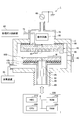
- FIG. 1 shows an example of the overall configuration of a substrate processing apparatus 1 according to an embodiment.
- the substrate processing apparatus 1 has a cylindrical chamber C.
- the chamber C is made of, for example, aluminum whose surface is anodized.
- a lower electrode 100 that also functions as a mounting table on which the substrate W is mounted is provided inside the chamber C.
- the lower electrode 100 is supported by a support body 110 provided via an insulating material 105.
- the upper electrode 50 is provided on the ceiling of the chamber C.
- the upper electrode 50 is electrically separated from the chamber C by an insulating material 55 disposed on the ceiling of the chamber C.
- the high frequency power supply 65 is connected to the upper electrode 50 through the matching circuit 60.
- the high frequency power supply 65 may be connected to the lower electrode 100 instead of being connected to the upper electrode 50.
- Two high frequency power supplies may be connected to the upper electrode and the lower electrode.
- Two high-frequency power sources may be connected to the lower electrode.
- the matching circuit 60 is provided in the matching box 70.
- the matching box 70 is a grounding housing for the matching circuit 60.
- the processing gas supply unit 80 is connected to the upper electrode 50 through a gas supply path 75.
- the desired gas output from the processing gas supply unit 80 passes through the gas supply path 75 and the upper electrode 50 and is supplied into the chamber C from the plurality of gas injection holes 95.
- the upper electrode 50 also functions as a gas shower head.
- a temperature sensor 85 is provided on the upper electrode 50. The temperature sensor 85 detects the temperature inside the chamber C.
- a bellows 15 is attached to the opening at the center of the bottom surface of the chamber C.
- the bellows 15 is fixed to the lifting plate 20.
- the elevating plate 20 adjusts the height at which the substrate W is placed by elevating.
- An impedance adjusting unit 30 is connected between the lower electrode 100 and the elevating plate 20 via a conductive path 25.
- the inside of the chamber C is decompressed to a desired degree of vacuum by the exhaust device 35.
- the substrate W is carried into the chamber C from the gate valve 40.
- Gas is supplied into the chamber C and high-frequency power is applied to the chamber C, whereby the substrate W is subjected to desired etching by the action of plasma generated from the gas.
- the control unit 200 includes a CPU (Central Processing Unit) 205, an HDD (Hard Disk Drive) 210, a ROM (Read Only Memory) 215, and a RAM (Random Access Memory) 220.
- the CPU 205, HDD 210, ROM 215, and RAM 220 are connected to each other via a bus B.
- the control unit 200 performs predetermined processing on the substrate W according to the processing procedure set in the process recipe.
- the process recipe is stored in the HDD 210 or the RAM 220.
- process conditions set values such as process time, temperature inside the chamber C (upper electrode temperature, side wall temperature of the processing chamber), pressure (gas exhaust), high-frequency power and voltage, and various gas flow rates are set.
- the control unit 200 compares the set temperature of the recipe with the detected temperature and adjusts the temperature inside the chamber C. Actual control is executed by the CPU 205.
- the CPU 205 performs processing such as etching on the substrate W according to the process recipe.
- the function of the control unit 200 may be realized by software or hardware.
- the overall configuration of the substrate processing apparatus 1 according to this embodiment has been described above.
- step conditions and all the processing procedures of the static elimination processes T1 and T2 are set in the process recipe. For this reason, it is necessary to change the set values for the common processes such as the static elimination processes T1 and T2 for each process recipe. In addition, an input mistake at the time of setting change is likely to occur.
- each unitized recipe is referred to as a “partial recipe”.
- the right side of FIG. 2 shows a partial recipe of a process condition recipe, a T1 recipe, and a T2 recipe as an example of a plurality of partial recipes obtained by dividing the processing procedure into functions.
- the process recipe in the file F1 of this embodiment is linked to each partial recipe of the process condition recipe, T1 recipe, and T2 recipe.
- the process recipe links to the process condition recipe, the T1 recipe, and the T2 recipe so that the processing procedures are executed in the order of the process condition recipe ⁇ the T1 recipe and the T2 recipe.
- the control unit 200 sequentially refers to the processing procedure set in the process condition recipe and the processing procedure set in the T1 recipe and the T2 recipe, and performs a predetermined process on the substrate W.
- the process condition recipe is an example of a partial recipe in which a processing procedure unique to substrate processing is set.
- the T1 recipe and the T2 recipe are examples of partial recipes in which processing procedures common to substrate processing are set.
- the partial recipe in which a specific processing procedure is set is a recipe in which process conditions, processing sequences, and processing timings specific to substrate processing such as etching processing and film formation processing are set.
- Specific process conditions include the type and flow rate of the etching gas, the pressure inside the chamber C, the temperature inside the chamber C, and the like.
- the partial recipe that sets a common processing procedure is a recipe that sets the process conditions, the processing sequence, and the processing timing in the pre-process and post-process of the substrate processing (main process) such as etching.
- the pre-process include seasoning for adjusting the condition in the chamber before processing the substrate and suction processing for sucking the substrate to the mounting table.
- the post-process there are a charge removal process for peeling the substrate from the mounting table and a cleaning process for cleaning the inside of the chamber C.
- FIG. 3 shows an example of the recipes (T1 recipe, T2 recipe) for the static elimination processes T1 and T2, which are examples of the post-process.
- FIG. 3 shows a T1 setting value (T1 recipe) and a T2 setting value (T2 recipe) for the recipe setting items.
- FIG. 3 shows the T1 and T2 set values of the items of the chamber pressure and the high frequency power of the upper RF and the lower RF, and other T1 and T2 set values are omitted for convenience.
- FIG. 4 An example of the charge removal processing sequence is shown in FIG.
- the left side of FIG. 4 shows a control example of the T1 (backside vacuuming) charge removal process
- the right side of FIG. 4 shows a control example of the T2 (chuck OFF) charge removal process.
- the T1 pressure set in the T1 recipe is set at the pressure control start timing in step S7 in the control example of the T1 static elimination process shown on the left side of FIG. 4, and the T1 set in the T1 recipe at the timings in steps S8 and S9.
- Lower power, T1 upper power is set.
- the T2 lower power and the T2 upper power set in the T2 recipe are set at the timings of steps S23 and S24 in the control example of the T2 static elimination process shown on the right side of FIG.
- the T1 recipe and the T2 recipe of the static elimination process in which a common process procedure is set are different from the process condition recipe (partial recipe) in which a unique process procedure is set. It is a partial recipe and is managed individually. Thereby, when a change occurs in the setting value of the T1 recipe or T2 recipe in which a common processing procedure is set, the setting value of the T1 recipe or T2 recipe may be changed. Thereby, the labor of input of an operator at the time of setting or changing a recipe is reduced, and input mistakes can be reduced. Thereby, setting, changing, and management of the process recipe can be facilitated.
- the process recipe of this embodiment is linked to the process condition recipe in which the processing procedure unique to the substrate processing is set, and the T1 recipe and the T2 recipe in which the processing procedure common to the substrate processing is set.
- the control part 200 can perform the process procedure of a process recipe combining several partial recipes.
- the processes common to the recipes are unitized, so that the partial recipe of the common process can be managed as a unit.
- the change can be applied to a plurality of process recipes that refer to the partial recipe only by changing the partial recipe in which the common process is unitized.
- work of the setting of a recipe or a setting change can be performed efficiently.
- FIG. 5 is a flowchart showing an example of processing of the substrate according to this embodiment.
- the control unit 200 applies a DC voltage to an electrode of an electrostatic chuck (not shown), and executes a process of electrostatically adsorbing the substrate to the mounting table (lower electrode 100) ( Step S12).
- the control unit 200 performs a predetermined process such as etching on the substrate (step S14).
- the controller 200 applies a DC voltage that is opposite in polarity to the DC voltage applied in step S12 to the electrode of the electrostatic chuck, and removes the substrate from the mounting table (step S16).
- the control unit 200 performs a process of cleaning the inside of the chamber C (step S18), and ends this process.
- the process recipe according to the present embodiment has link information to a plurality of partial recipes in which processing procedures are divided into functions and unitized.
- the control unit 200 refers to the linked partial recipe based on the link information included in the process recipe, and controls the processing of the substrate according to the processing procedure set in the linked partial recipe. Thereby, a desired process is performed on the substrate.
- the plurality of partial recipes include a partial recipe in which a processing procedure unique to the substrate processing is set, and a partial recipe in which a processing procedure common to the substrate processing is set.
- An example of a partial recipe in which a processing procedure unique to the processing of the substrate W is set is shown on the right side of FIG.
- examples of partial recipes that set unique processing procedures linked to the process recipe include etching recipes 1 and 2 and ashing. Recipes are listed.
- the partial recipe in which the processing procedure unique to the substrate processing is set may include a plurality of partial recipes in which the processing procedure of each step is set when the processing procedure unique to the substrate processing is divided into a plurality of steps.
- the etching recipe 1 can be divided into functions and divided into a plurality of partial recipes.
- the etching recipe 1 is a recipe in which a processing procedure for etching a laminated film is set, the process conditions for etching each layer of the laminated film are different. Therefore, the etching recipe 1 can be divided into a bark layer etching recipe, an oxide layer etching recipe, and a nitride layer etching recipe.
- the process recipe according to the present embodiment can refer to each partial recipe by having link information of a bark layer etching recipe, an oxide layer etching recipe, and a nitride layer etching recipe.
- the etching recipe 2 can be divided into a main recipe and a partial recipe of an overetch recipe. Further, although not shown, when the main etching process is divided into a plurality of steps of an oxide film etching step and a polysilicon film etching step, the main etching recipe is further divided into an oxide film etching recipe and a polysilicon film etching recipe. Can be divided into
- the partial recipe in which the processing procedure common to the substrate processing is set includes a partial recipe in which at least one of the pre-processing and post-processing processing specific to the substrate processing is set.
- An example of a partial recipe in which a processing procedure common to the processing of the substrate W is set is shown on the left side of FIG.
- the substrate suction recipe for setting the procedure of the substrate suction process in step S12, which is a pre-process of the process in step S14 in which the unique process is executed is an example of a partial recipe in which a process procedure common to the substrate processing is set. is there.
- partial recipe in which the processing procedure common to the substrate processing is set include the substrate discharging recipes T1 and T2 for setting the substrate discharging processing procedure in step S16, and the mounting table discharging recipe.
- the partial recipe in which the processing procedure common to the substrate processing is set there is a cleaning recipe in which the cleaning processing procedure in step S18 is set.
- a process recipe can be linked to a plurality of process condition recipes A, B, and C as partial recipes for setting a processing procedure unique to substrate processing.
- the process condition recipe A is a bark layer etching recipe
- the process condition recipe B is an oxide layer etching recipe
- process condition recipe C is a nitride layer etching recipe.
- the process recipe is linked to the post-processing T1 recipe and T2 recipe as a partial recipe for setting processing common to the processing of the substrate W.
- the process recipe may be linked to a preprocessing substrate suction recipe or a postprocessing cleaning recipe as a partial recipe for setting processing common to substrate processing.
- the process recipe is linked to one or a plurality of partial recipes set with processing procedures unique to the substrate processing and one or a plurality of partial recipes set with processing procedures common to the substrate processing. be able to.
- a plurality of unitized partial recipes can be designated from a plurality of process recipes and used in common.
- the process condition recipe A in the file F2 and the process condition recipe B in the file F3 are linked to the T1 recipe and the T2 recipe.
- the T1 recipe and the T2 recipe are referred to from the process condition recipe A and the process condition recipe B, and the processing procedure set in the T1 recipe and the T2 recipe is used in the process condition recipe A and the process condition recipe B. be able to.
- the process condition recipe A is an oxide film etching recipe and the process condition recipe B is a polysilicon film etching recipe
- only the process condition recipe A needs to be changed when it is desired to change the oxide film etching process.
- the processing procedure for etching the polysilicon film is desired to be changed
- only the process condition recipe B need be changed.
- it is desired to change the charge removal processing procedure only the T1 and T2 recipes need be changed.
- setting, change of settings, and management can be performed in units of partial recipes that are unitized by function, so that the labor of input work is saved and recipe management is performed efficiently. be able to.
- the partial recipe may include a recipe in which an error processing procedure is set.
- the process recipe in the file F1 may include not only the processing procedure set for a plurality of partial recipes but also a processing procedure that branches depending on a predetermined condition.
- the branch process is executed in the process procedure described in the process condition recipe, if a predetermined condition is not satisfied, an error in the static elimination process set in the T1 recipe (error process) and the T2 recipe (error process) is detected.
- a processing procedure is executed. At this time, the normal processing procedure in the static elimination processing set in the T1 recipe and the T2 recipe is not executed.
- the predetermined condition when the predetermined condition is satisfied, the normal processing procedure in the static elimination process set in the T1 recipe and the T2 recipe is executed, and in the static elimination process set in the T1 recipe (error process) and the T2 recipe (error process).
- the error procedure is not executed.
- the partial recipe according to predetermined conditions can be referred.
- the process recipe in the file F1 may be linked not only to the process condition recipe, T1 recipe and T2 recipe but also to a macro program (hereinafter also referred to as “macro”).
- the control unit 200 controls the processing of the substrate according to the sequence defined in the linked macro.
- a relatively small processing unit procedure such as particle check or valve opening / closing setting can be set in a process recipe using a macro.
- NPPC Non-Plasma Particle Cleaning
- a purge gas shock wave is generated by intermittently supplying a voltage from a DC power source (not shown) into the chamber C while allowing the purge gas to flow into and out of the chamber C.
- Particles in the chamber are removed by the electromagnetic vibration based on the physical vibration caused by the electric field and the potential gradient instantaneously formed on the apparatus wall surface or the mounting table.
- the NPPC conditions may be set in the process recipe using a macro. By linking a process recipe to a macro, the function of the macro can be referenced from the process recipe.
- the process recipe in the file F1 may be linked to the check program by calling the auto check program via a macro.
- the present invention is not limited to this, and the process recipe may directly call the auto check program without using a macro.
- the control unit 200 checks whether the substrate processing apparatus is in a normal state according to the check items defined in the linked check program.
- Figure 10 shows an example of items checked by the auto check program.
- the auto check program it is possible to automatically check the check items such as the ultimate pressure value and leak value inside the chamber C, the flow rate value of the gas flowing into the chamber C, and the adhesion state of particles (depots).
- the macro linked by the process recipe starts the auto check program, thereby realizing the zero point adjustment sequence check of the gas flow meter shown in steps S20 to S48 of FIG. Is done.
- a detailed description of the processes in steps S20 to S48 will be omitted.
- the auto check program may be started directly by a process recipe.
- a partial recipe (for example, T1, T2 recipe) in which a common processing procedure is set and a partial recipe (for example, a specific processing procedure is set) And process condition recipes) can be managed individually.
- process condition recipes for example, a change in a partial recipe that sets a common process is reflected in all process recipes that link and refer to the partial recipe. Therefore, it is not necessary to change the setting of the common processing part included in the process recipe in which the entire processing procedure is set as in the past. For this reason, the labor of a worker can be saved by significantly reducing the amount of work for setting the recipe and changing the setting. Thereby, setting, changing, and management of the process recipe can be facilitated.
- FIG. 12 shows an example of a recipe and a partial recipe used for explaining this modification.
- the transfer recipe a transfer route, transfer timing, and the like when transferring the wafer W are set.
- the transfer recipe is linked to recipes such as a load lock module recipe and a process recipe.
- the load lock module recipe wafer loading / unloading, supply / exhaust timing, and the like in the load lock module are set.
- the process recipe is linked to the substrate adsorption recipe, the substrate processing recipe, the substrate charge removal recipe, and the cleaning partial recipes.
- the substrate adsorption recipe conditions for adsorbing the wafer to the mounting table are set.
- Process conditions for processing a wafer are set in the substrate processing recipe.
- the substrate neutralization recipe conditions for detaching the wafer from the mounting table are set.
- Conditions for cleaning the inside of the chamber are set in the cleaning recipe.
- the knowledge of the operation of the substrate processing apparatus 1 and the contents of the recipe are greatly different between the workers in the design process and the workers in the mass production process. Therefore, the same screen is displayed in the mass production process and the design process, and it is desired to prevent an operation error from occurring on the operation on the screen.
- screens corresponding to the reference authority and the editing authority are displayed in the mass production process and the design process, and work errors are reduced.
- the reference authority and the editing authority may be set in advance by the administrator, or may be changed by the administrator during work.
- An example of reference authority and edit authority is shown in FIG.
- the main recipe is a transfer recipe, a load lock module recipe, and a process recipe.
- the transfer recipe has reference authority and edit authority in the mass production process and the design process.
- the load lock module recipe and the process recipe have reference authority and edit authority in the mass production process and the design process.
- the substrate adsorption recipe, substrate processing recipe, substrate static elimination recipe, and cleaning recipe are partial recipes linked to the process recipe. These partial recipes have reference authority and edit authority in the design process. Also, these partial recipes do not have editing authority in the mass production process. These partial recipes can be selected with or without reference authority in the mass production process.
- the editing authority set for each of the process recipe and the plurality of partial recipes is an example of first authority information indicating the authority to edit each of the process recipe and the plurality of partial recipes.
- the reference authority set for each of the process recipe and the plurality of partial recipes is an example of second authority information indicating the authority to refer to each of the process recipe and the plurality of partial recipes.
- the control unit 200 controls whether to edit the process recipe and the plurality of partial recipes on the screen based on the authority to edit each of the process recipe and the plurality of partial recipes.
- control unit 200 controls whether or not the process recipe and the plurality of partial recipes can be referred to on the screen based on the authority to refer to each of the process recipe and the plurality of partial recipes.
- FIG. 14 shows an example of a screen when the administrator selects “Yes” in the reference authority of the mass production process for the substrate suction recipe, the substrate processing recipe, the substrate static elimination recipe, and the cleaning recipe.
- FIG. 14A and 14B are examples of a recipe setting screen displayed on the display 305 of the PC 300 having the control unit 200 of FIG.
- FIG. 14A is an example of a setting screen in the mass production process
- FIG. 14B is an example of a setting screen in the design process.
- the transfer recipe display area 301, the load lock module recipe display area 311 and the process recipe display area 312 are displayed so that the items in each recipe can be edited.
- the display area 321 of the substrate adsorption recipe, the display area 322 of the substrate processing recipe, the display area 323 of the substrate static elimination recipe, and the display area 324 of the cleaning recipe can only refer to the items in each recipe (that is, cannot be edited). ) Is displayed.
- the hierarchy that can be edited by the operator can be divided into the main recipe and the partial recipe. That is, in the mass production process, the operator can edit each item of the transfer recipe, the load lock module recipe, and the process recipe. On the other hand, the operator can only refer to the substrate suction recipe, the substrate processing recipe, the substrate charge removal recipe, and the cleaning recipe, and cannot edit each item of these partial recipes.
- FIG. 14B is an example of a setting screen in the design process. In the design process, all recipes and partial recipes on the screen can be edited.
- FIG. 15 shows another example of the recipe setting screen displayed on the display 305.
- the substrate processing recipe 322 is not displayed in the mass production process.
- the authority to refer to the substrate processing recipe shown in FIG. 13 is set to “none”, and the authority to refer to other partial recipes is set to “present”.
- the substrate suction recipe display area 321, the substrate neutralization recipe display area 323, and the cleaning recipe display area 324 are displayed so that items in each recipe can be referred to and cannot be edited. Has been.
- the display area 322 of the substrate processing recipe is not displayed. Thereby, the display of the display 305 can be controlled so that the process conditions of the substrate processing recipe cannot be referred to. In this case, the same screen as FIG. 14B is displayed in the design process.
- the operator can edit the transfer recipe, the load lock module recipe, and the process recipe in the mass production process.
- the operator can refer to the substrate suction recipe, the substrate charge removal recipe, and the cleaning recipe, but cannot edit the recipe. Further, the operator cannot refer to the substrate processing recipe.
- the editing authority and reference authority in the mass production process and the design process it is possible to reduce work mistakes that erroneously change settings on the screen and to limit the disclosure of information such as process conditions. it can.
- the substrate processing apparatus is applicable not only to a capacitively coupled plasma (CCP) apparatus but also to other substrate processing apparatuses.
- Other substrate processing devices include inductively coupled plasma (ICP), CVD (chemical vapor deposition) devices using radial line slot antennas, helicon wave excited plasma (HWP) devices, electronic It may be a cyclotron resonance plasma (ECR: ElectroncloCyclotron Resonance Plasma) device or the like.
- the substrate processed by the substrate processing apparatus according to the present invention may be a wafer, a large substrate for a flat panel display, an EL element, or a substrate for a solar cell.
- Substrate processing apparatus 50 Upper electrode 100: Lower electrode (mounting table) 200: Control unit 205: CPU 210: HDD 215: ROM 220: RAM C: Chamber
Landscapes
- Engineering & Computer Science (AREA)
- Physics & Mathematics (AREA)
- Condensed Matter Physics & Semiconductors (AREA)
- General Physics & Mathematics (AREA)
- Manufacturing & Machinery (AREA)
- Computer Hardware Design (AREA)
- Microelectronics & Electronic Packaging (AREA)
- Power Engineering (AREA)
- Plasma & Fusion (AREA)
- Chemical & Material Sciences (AREA)
- Analytical Chemistry (AREA)
- Drying Of Semiconductors (AREA)
Abstract
Description
まず、本発明の一実施形態に係る基板処理装置1の全体構成の一例について、図1を参照しながら説明する。図1は、一実施形態に係る基板処理装置1の全体構成の一例を示す。
次に、本実施形態に係るプロセスレシピの構成の一例について、図2を参照しながら説明する。図2の右側には、本実施形態に係るプロセスレシピの構成の一例が示されている。図2の左側には、一つの基板の処理に対して一つのプロセスレシピが作成されている。ファイルF0内のプロセスレシピに基板を処理するためのメインプロセスのステップ条件及び後工程の除電処理T1、T2のすべての処理手順が設定されている例を示している。
次に、本実施形態に係る基板の処理の一例について図5を参照しながら説明する。図5は、本実施形態に係る基板の処理の一例を示すフローチャートを示す。基板がチャンバCの内部に搬入されると、制御部200は、図示しない静電チャックの電極に直流電圧を印加し、基板を載置台(下部電極100)に静電吸着させる処理を実行する(ステップS12)。次に、制御部200は、基板にエッチング等の所定の処理を実行する(ステップS14)。次に、制御部200は、静電チャックの電極にステップS12にて印加した直流電圧と正負が逆の直流電圧を印加して除電し、基板を載置台から離脱させる(ステップS16)。制御部200は、基板をチャンバCから搬出させた後、チャンバCの内部をクリーニングする処理を実行し(ステップS18)、本処理を終了する。
図6に示すように、プロセスレシピは、基板の処理に固有の処理手順を設定する部分レシピとして複数のプロセス条件レシピA、B、Cにリンクすることが可能である。例えば、図5に示すフローチャートにより基板上に形成されたバーク層、オキサイド層及びナイトライド層の積層膜のエッチング処理が実行される場合、プロセス条件レシピAはバーク層エッチングレシピであり、プロセス条件レシピBはオキサイド層エッチングレシピであり、プロセス条件レシピCはナイトライド層エッチングレシピとなる。
図7に示すように、ユニット化した複数の部分レシピは、複数のプロセスレシピから指定され、共通して使用されることが可能である。図7ではファイルF2内のプロセス条件レシピA及びファイルF3内のプロセス条件レシピBは、T1レシピ及びT2レシピにリンクする。これにより、T1レシピ及びT2レシピは、プロセス条件レシピA及びプロセス条件レシピBから参照されることで、T1レシピ及びT2レシピに設定された処理手順をプロセス条件レシピA及びプロセス条件レシピBで使用することができる。これにより、プロセスレシピ毎にT1レシピやT2レシピに設定された処理手順をそれぞれ定義する手間を省くことができる。
部分レシピには、エラー処理の手順を設定したレシピが含まれてもよい。図8に示すように、ファイルF1内のプロセスレシピは、複数の部分レシピに設定された処理手順を実行するだけでなく、所定の条件によって分岐する処理手順を含んでもよい。ここでは、プロセス条件レシピに記述した処理手順において分岐処理を実行する際、所定の条件を満たさない場合、T1レシピ(エラー処理)及びT2レシピ(エラー処理)に設定された除電処理におけるエラー時の処理手順が実行される。このとき、T1レシピ及びT2レシピに設定された除電処理における通常時の処理手順は実行されない。
また、図9に示すように、ファイルF1内のプロセスレシピは、プロセス条件レシピ、T1レシピ及びT2レシピだけなく、マクロプログラム(以下、「マクロ」ともいう。)にリンクしてもよい。その場合、制御部200は、リンクしたマクロに定められたシーケンスに従い基板の処理を制御する。
次に、本実施形態の変形例について図12~図15を参照しながら説明する。本実施形態の変形例では、レシピ及び部分レシピの設定項目の編集及び参照の可否を制御する。図12に、本変形例の説明に使用するレシピ及び部分レシピの一例を示す。
50:上部電極
100:下部電極(載置台)
200:制御部
205:CPU
210:HDD
215:ROM
220:RAM
C:チャンバ
Claims (10)
- プロセスレシピに設定された処理手順に従い基板の処理を制御する制御部を備える基板処理装置であって、
前記プロセスレシピは、前記処理手順を機能別に分けてユニット化した複数の部分レシピにリンクし、
前記制御部は、
リンクした前記複数の部分レシピに設定された処理手順に従い基板の処理を制御する、
基板処理装置。 - 前記複数の部分レシピは、基板の処理に固有の処理手順を設定した部分レシピと、基板の処理に共通の処理手順を設定した部分レシピとを含む、
請求項1に記載の基板処理装置。 - 前記固有の処理手順を設定した部分レシピは、基板の処理に固有の処理手順を複数の工程に分けたときの各工程の処理手順を設定した複数の部分レシピを含む、
請求項2に記載の基板処理装置。 - 前記共通の処理手順を設定した部分レシピは、前記固有の処理手順により実行される処理の前工程及び後工程の少なくともいずれかの処理手順を設定した部分レシピを含む、
請求項2に記載の基板処理装置。 - 前記プロセスレシピは、
マクロプログラムにリンクし、
前記制御部は、
リンクした前記マクロプログラムに定められたシーケンスに従い、基板の処理を制御する、
請求項1に記載の基板処理装置。 - 前記プロセスレシピは、
チェックプログラムにリンクし、
前記制御部は、
リンクした前記チェックプログラムに定められたチェック項目に従い、前記基板処理装置の状態をチェックする、
請求項1に記載の基板処理装置。 - 基板の処理手順を設定するプロセスレシピにより基板に処理を施す基板処理方法であって、
前記処理手順を機能別に分けてユニット化した複数の部分レシピにリンクするプロセスレシピを生成する手段と、
前記プロセスレシピにリンクした複数の部分レシピに設定された処理手順に従い、基板に処理を施す手段と、
を含む基板処理方法。 - 基板の処理手順を設定するプロセスレシピにより基板を処理するための基板処理プログラムであって、
前記処理手順を機能別に分けてユニット化した複数の部分レシピとリンクしたプロセスレシピを生成する処理と、
前記プロセスレシピにリンクした複数の部分レシピに設定された処理手順に従い、基板に処理を施す処理と、
を含む基板処理プログラム。 - 前記制御部は、
前記プロセスレシピ及び前記複数の部分レシピのそれぞれについて編集する権限を示す第1の権限情報に基づき、前記プロセスレシピ及び前記複数の部分レシピの画面上における編集の可否を制御する、
請求項1に記載の基板処理装置。 - 前記制御部は、
前記プロセスレシピ及び前記複数の部分レシピのそれぞれについて参照する権限を示す第2の権限情報に基づき、前記プロセスレシピ及び前記複数の部分レシピの画面上における参照の可否を制御する、
請求項1に記載の基板処理装置。
Priority Applications (3)
| Application Number | Priority Date | Filing Date | Title |
|---|---|---|---|
| US15/304,570 US10128121B2 (en) | 2014-05-20 | 2015-05-18 | Substrate processing apparatus, substrate processing method and substrate processing program |
| KR1020167020130A KR102364319B1 (ko) | 2014-05-20 | 2015-05-18 | 기판 처리 장치, 기판 처리 방법 및 기판 처리 프로그램 |
| CN201580020853.4A CN106233427B (zh) | 2014-05-20 | 2015-05-18 | 基板处理装置和基板处理方法 |
Applications Claiming Priority (4)
| Application Number | Priority Date | Filing Date | Title |
|---|---|---|---|
| JP2014-104206 | 2014-05-20 | ||
| JP2014104206 | 2014-05-20 | ||
| JP2015-087044 | 2015-04-21 | ||
| JP2015087044A JP6501601B2 (ja) | 2014-05-20 | 2015-04-21 | 基板処理装置、基板処理方法及び基板処理プログラム |
Publications (1)
| Publication Number | Publication Date |
|---|---|
| WO2015178348A1 true WO2015178348A1 (ja) | 2015-11-26 |
Family
ID=54554018
Family Applications (1)
| Application Number | Title | Priority Date | Filing Date |
|---|---|---|---|
| PCT/JP2015/064214 WO2015178348A1 (ja) | 2014-05-20 | 2015-05-18 | 基板処理装置、基板処理方法及び基板処理プログラム |
Country Status (6)
| Country | Link |
|---|---|
| US (1) | US10128121B2 (ja) |
| JP (1) | JP6501601B2 (ja) |
| KR (1) | KR102364319B1 (ja) |
| CN (1) | CN106233427B (ja) |
| TW (1) | TWI684664B (ja) |
| WO (1) | WO2015178348A1 (ja) |
Cited By (1)
| Publication number | Priority date | Publication date | Assignee | Title |
|---|---|---|---|---|
| JPWO2021241242A1 (ja) * | 2020-05-25 | 2021-12-02 |
Families Citing this family (5)
| Publication number | Priority date | Publication date | Assignee | Title |
|---|---|---|---|---|
| JP6517845B2 (ja) * | 2017-01-17 | 2019-05-22 | 株式会社荏原製作所 | スケジューラ、基板処理装置、及び基板搬送方法 |
| JP6586443B2 (ja) * | 2017-10-10 | 2019-10-02 | 東京エレクトロン株式会社 | 被処理体を処理する方法 |
| WO2019159735A1 (ja) * | 2018-02-16 | 2019-08-22 | 東京エレクトロン株式会社 | 加工装置 |
| JP7226949B2 (ja) * | 2018-09-20 | 2023-02-21 | 株式会社Screenホールディングス | 基板処理装置および基板処理システム |
| WO2024185561A1 (ja) * | 2023-03-06 | 2024-09-12 | 東京エレクトロン株式会社 | コンピュータプログラム、情報処理方法及び情報処理装置 |
Citations (3)
| Publication number | Priority date | Publication date | Assignee | Title |
|---|---|---|---|---|
| JPH0982589A (ja) * | 1995-09-18 | 1997-03-28 | Kokusai Electric Co Ltd | 半導体製造装置の処理システム |
| JP2009054674A (ja) * | 2007-08-24 | 2009-03-12 | Tokyo Electron Ltd | 製造装置、操作ログ蓄積方法、及びプログラム |
| JP2010505209A (ja) * | 2006-09-28 | 2010-02-18 | ラム リサーチ コーポレーション | 汎用方法を利用したレシピ作成方法および装置 |
Family Cites Families (4)
| Publication number | Priority date | Publication date | Assignee | Title |
|---|---|---|---|---|
| JP3708031B2 (ja) * | 2001-06-29 | 2005-10-19 | 株式会社日立製作所 | プラズマ処理装置および処理方法 |
| US7292906B2 (en) * | 2004-07-14 | 2007-11-06 | Tokyo Electron Limited | Formula-based run-to-run control |
| JP5128080B2 (ja) | 2006-03-29 | 2013-01-23 | 東京エレクトロン株式会社 | 基板処理装置の制御装置およびその制御方法 |
| JP5028193B2 (ja) * | 2007-09-05 | 2012-09-19 | 株式会社日立ハイテクノロジーズ | 半導体製造装置における被処理体の搬送方法 |
-
2015
- 2015-04-21 JP JP2015087044A patent/JP6501601B2/ja active Active
- 2015-05-18 WO PCT/JP2015/064214 patent/WO2015178348A1/ja active Application Filing
- 2015-05-18 US US15/304,570 patent/US10128121B2/en active Active
- 2015-05-18 KR KR1020167020130A patent/KR102364319B1/ko active IP Right Grant
- 2015-05-18 CN CN201580020853.4A patent/CN106233427B/zh active Active
- 2015-05-18 TW TW104115712A patent/TWI684664B/zh active
Patent Citations (3)
| Publication number | Priority date | Publication date | Assignee | Title |
|---|---|---|---|---|
| JPH0982589A (ja) * | 1995-09-18 | 1997-03-28 | Kokusai Electric Co Ltd | 半導体製造装置の処理システム |
| JP2010505209A (ja) * | 2006-09-28 | 2010-02-18 | ラム リサーチ コーポレーション | 汎用方法を利用したレシピ作成方法および装置 |
| JP2009054674A (ja) * | 2007-08-24 | 2009-03-12 | Tokyo Electron Ltd | 製造装置、操作ログ蓄積方法、及びプログラム |
Cited By (4)
| Publication number | Priority date | Publication date | Assignee | Title |
|---|---|---|---|---|
| JPWO2021241242A1 (ja) * | 2020-05-25 | 2021-12-02 | ||
| WO2021240572A1 (ja) * | 2020-05-25 | 2021-12-02 | 株式会社日立ハイテク | 半導体装置製造システムおよび半導体装置製造方法 |
| WO2021241242A1 (ja) * | 2020-05-25 | 2021-12-02 | 株式会社日立ハイテク | 半導体装置製造システムおよび半導体装置製造方法 |
| JP7149428B2 (ja) | 2020-05-25 | 2022-10-06 | 株式会社日立ハイテク | 半導体装置製造システムおよび半導体装置製造方法 |
Also Published As
| Publication number | Publication date |
|---|---|
| CN106233427A (zh) | 2016-12-14 |
| TW201610210A (zh) | 2016-03-16 |
| KR102364319B1 (ko) | 2022-02-16 |
| TWI684664B (zh) | 2020-02-11 |
| JP6501601B2 (ja) | 2019-04-17 |
| CN106233427B (zh) | 2019-07-09 |
| US20170040177A1 (en) | 2017-02-09 |
| KR20170004951A (ko) | 2017-01-11 |
| US10128121B2 (en) | 2018-11-13 |
| JP2016001726A (ja) | 2016-01-07 |
Similar Documents
| Publication | Publication Date | Title |
|---|---|---|
| WO2015178348A1 (ja) | 基板処理装置、基板処理方法及び基板処理プログラム | |
| JP6219229B2 (ja) | ヒータ給電機構 | |
| TW201740501A (zh) | 晶圓傳送用的晶圓升降環系統 | |
| US11037815B2 (en) | Dechuck control method and plasma processing apparatus | |
| KR102302313B1 (ko) | 재치대에 피흡착물을 흡착시키는 방법 및 플라즈마 처리 장치 | |
| KR102490646B1 (ko) | 기판 처리 장치의 제어 장치 및 기판 처리 표시 방법 | |
| JP6219227B2 (ja) | ヒータ給電機構及びステージの温度制御方法 | |
| KR102538188B1 (ko) | 플라즈마 처리 장치의 세정 방법 | |
| US10553409B2 (en) | Method of cleaning plasma processing apparatus | |
| US10991551B2 (en) | Cleaning method and plasma processing apparatus | |
| KR102427971B1 (ko) | 플라즈마 처리 방법 | |
| JP2010267708A (ja) | 真空処理装置および真空処理方法 | |
| US9922841B2 (en) | Plasma processing method | |
| JP7512037B2 (ja) | 載置台、基板処理装置及び伝熱ガス供給方法 | |
| JP2023038801A (ja) | 基板処理方法 | |
| US20240212979A1 (en) | Method for determining amount of wear of edge ring, plasma processing apparatus, and substrate processing system | |
| WO2024095840A1 (ja) | 基板処理装置、基板処理システム、およびクリーニング方法 | |
| US20240347325A1 (en) | Plasma processing apparatus | |
| WO2023042804A1 (ja) | プラズマ処理装置及びプラズマ処理方法 | |
| US20230282452A1 (en) | Cleaning method, method of manufacturing semiconductor device, plasma treatment device, and outer circumferential ring set | |
| JP2024110176A (ja) | エッジリング及びエッジリング取付方法 | |
| TW202330120A (zh) | 清潔方法、基板之處理方法及電漿處理裝置 | |
| KR20220085452A (ko) | 기판 처리 장치 및 기판 처리 방법 | |
| JP2022036719A (ja) | 基板処理方法及び基板処理装置 |
Legal Events
| Date | Code | Title | Description |
|---|---|---|---|
| 121 | Ep: the epo has been informed by wipo that ep was designated in this application |
Ref document number: 15796714 Country of ref document: EP Kind code of ref document: A1 |
|
| ENP | Entry into the national phase |
Ref document number: 20167020130 Country of ref document: KR Kind code of ref document: A |
|
| WWE | Wipo information: entry into national phase |
Ref document number: 15304570 Country of ref document: US |
|
| NENP | Non-entry into the national phase |
Ref country code: DE |
|
| 122 | Ep: pct application non-entry in european phase |
Ref document number: 15796714 Country of ref document: EP Kind code of ref document: A1 |