WO2015156023A1 - 絶縁ゲート型半導体装置、及び、絶縁ゲート型半導体装置の製造方法 - Google Patents
絶縁ゲート型半導体装置、及び、絶縁ゲート型半導体装置の製造方法 Download PDFInfo
- Publication number
- WO2015156023A1 WO2015156023A1 PCT/JP2015/053692 JP2015053692W WO2015156023A1 WO 2015156023 A1 WO2015156023 A1 WO 2015156023A1 JP 2015053692 W JP2015053692 W JP 2015053692W WO 2015156023 A1 WO2015156023 A1 WO 2015156023A1
- Authority
- WO
- WIPO (PCT)
- Prior art keywords
- region
- trench
- outer peripheral
- forming
- semiconductor substrate
- Prior art date
Links
- 239000004065 semiconductor Substances 0.000 title claims abstract description 123
- 238000004519 manufacturing process Methods 0.000 title claims description 31
- 230000002093 peripheral effect Effects 0.000 claims abstract description 139
- 239000000758 substrate Substances 0.000 claims abstract description 71
- 239000012535 impurity Substances 0.000 claims description 42
- 238000000034 method Methods 0.000 claims description 17
- 238000000137 annealing Methods 0.000 claims description 16
- 238000009792 diffusion process Methods 0.000 claims description 11
- 229910052799 carbon Inorganic materials 0.000 claims description 10
- OKTJSMMVPCPJKN-UHFFFAOYSA-N Carbon Chemical compound [C] OKTJSMMVPCPJKN-UHFFFAOYSA-N 0.000 claims description 9
- 229910052796 boron Inorganic materials 0.000 claims description 9
- ZOXJGFHDIHLPTG-UHFFFAOYSA-N Boron Chemical compound [B] ZOXJGFHDIHLPTG-UHFFFAOYSA-N 0.000 claims description 8
- 210000000746 body region Anatomy 0.000 description 17
- 230000005684 electric field Effects 0.000 description 9
- 230000015556 catabolic process Effects 0.000 description 6
- 238000010586 diagram Methods 0.000 description 5
- 238000005192 partition Methods 0.000 description 4
- 238000005516 engineering process Methods 0.000 description 3
- 238000002513 implantation Methods 0.000 description 3
- 239000012212 insulator Substances 0.000 description 3
- 230000004048 modification Effects 0.000 description 3
- 238000012986 modification Methods 0.000 description 3
- XAGFODPZIPBFFR-UHFFFAOYSA-N aluminium Chemical compound [Al] XAGFODPZIPBFFR-UHFFFAOYSA-N 0.000 description 2
- 229910052782 aluminium Inorganic materials 0.000 description 2
- 239000012141 concentrate Substances 0.000 description 2
- 238000005530 etching Methods 0.000 description 2
- 238000009826 distribution Methods 0.000 description 1
- 230000000694 effects Effects 0.000 description 1
- 238000005468 ion implantation Methods 0.000 description 1
- 239000000463 material Substances 0.000 description 1
- 229910003465 moissanite Inorganic materials 0.000 description 1
- HBMJWWWQQXIZIP-UHFFFAOYSA-N silicon carbide Chemical compound [Si+]#[C-] HBMJWWWQQXIZIP-UHFFFAOYSA-N 0.000 description 1
- 229910010271 silicon carbide Inorganic materials 0.000 description 1
Images


Classifications
-
- H—ELECTRICITY
- H10—SEMICONDUCTOR DEVICES; ELECTRIC SOLID-STATE DEVICES NOT OTHERWISE PROVIDED FOR
- H10D—INORGANIC ELECTRIC SEMICONDUCTOR DEVICES
- H10D12/00—Bipolar devices controlled by the field effect, e.g. insulated-gate bipolar transistors [IGBT]
- H10D12/01—Manufacture or treatment
- H10D12/031—Manufacture or treatment of IGBTs
-
- H—ELECTRICITY
- H10—SEMICONDUCTOR DEVICES; ELECTRIC SOLID-STATE DEVICES NOT OTHERWISE PROVIDED FOR
- H10D—INORGANIC ELECTRIC SEMICONDUCTOR DEVICES
- H10D62/00—Semiconductor bodies, or regions thereof, of devices having potential barriers
- H10D62/10—Shapes, relative sizes or dispositions of the regions of the semiconductor bodies; Shapes of the semiconductor bodies
-
- H—ELECTRICITY
- H01—ELECTRIC ELEMENTS
- H01L—SEMICONDUCTOR DEVICES NOT COVERED BY CLASS H10
- H01L21/00—Processes or apparatus adapted for the manufacture or treatment of semiconductor or solid state devices or of parts thereof
- H01L21/02—Manufacture or treatment of semiconductor devices or of parts thereof
- H01L21/04—Manufacture or treatment of semiconductor devices or of parts thereof the devices having potential barriers, e.g. a PN junction, depletion layer or carrier concentration layer
- H01L21/0445—Manufacture or treatment of semiconductor devices or of parts thereof the devices having potential barriers, e.g. a PN junction, depletion layer or carrier concentration layer the devices having semiconductor bodies comprising crystalline silicon carbide
- H01L21/0455—Making n or p doped regions or layers, e.g. using diffusion
- H01L21/046—Making n or p doped regions or layers, e.g. using diffusion using ion implantation
-
- H—ELECTRICITY
- H01—ELECTRIC ELEMENTS
- H01L—SEMICONDUCTOR DEVICES NOT COVERED BY CLASS H10
- H01L21/00—Processes or apparatus adapted for the manufacture or treatment of semiconductor or solid state devices or of parts thereof
- H01L21/70—Manufacture or treatment of devices consisting of a plurality of solid state components formed in or on a common substrate or of parts thereof; Manufacture of integrated circuit devices or of parts thereof
- H01L21/71—Manufacture of specific parts of devices defined in group H01L21/70
- H01L21/76—Making of isolation regions between components
- H01L21/762—Dielectric regions, e.g. EPIC dielectric isolation, LOCOS; Trench refilling techniques, SOI technology, use of channel stoppers
- H01L21/76224—Dielectric regions, e.g. EPIC dielectric isolation, LOCOS; Trench refilling techniques, SOI technology, use of channel stoppers using trench refilling with dielectric materials
- H01L21/76237—Dielectric regions, e.g. EPIC dielectric isolation, LOCOS; Trench refilling techniques, SOI technology, use of channel stoppers using trench refilling with dielectric materials introducing impurities in trench side or bottom walls, e.g. for forming channel stoppers or alter isolation behavior
-
- H—ELECTRICITY
- H10—SEMICONDUCTOR DEVICES; ELECTRIC SOLID-STATE DEVICES NOT OTHERWISE PROVIDED FOR
- H10D—INORGANIC ELECTRIC SEMICONDUCTOR DEVICES
- H10D30/00—Field-effect transistors [FET]
- H10D30/01—Manufacture or treatment
- H10D30/021—Manufacture or treatment of FETs having insulated gates [IGFET]
- H10D30/028—Manufacture or treatment of FETs having insulated gates [IGFET] of double-diffused metal oxide semiconductor [DMOS] FETs
- H10D30/0291—Manufacture or treatment of FETs having insulated gates [IGFET] of double-diffused metal oxide semiconductor [DMOS] FETs of vertical DMOS [VDMOS] FETs
- H10D30/0297—Manufacture or treatment of FETs having insulated gates [IGFET] of double-diffused metal oxide semiconductor [DMOS] FETs of vertical DMOS [VDMOS] FETs using recessing of the gate electrodes, e.g. to form trench gate electrodes
-
- H—ELECTRICITY
- H10—SEMICONDUCTOR DEVICES; ELECTRIC SOLID-STATE DEVICES NOT OTHERWISE PROVIDED FOR
- H10D—INORGANIC ELECTRIC SEMICONDUCTOR DEVICES
- H10D30/00—Field-effect transistors [FET]
- H10D30/60—Insulated-gate field-effect transistors [IGFET]
-
- H—ELECTRICITY
- H10—SEMICONDUCTOR DEVICES; ELECTRIC SOLID-STATE DEVICES NOT OTHERWISE PROVIDED FOR
- H10D—INORGANIC ELECTRIC SEMICONDUCTOR DEVICES
- H10D30/00—Field-effect transistors [FET]
- H10D30/60—Insulated-gate field-effect transistors [IGFET]
- H10D30/64—Double-diffused metal-oxide semiconductor [DMOS] FETs
- H10D30/66—Vertical DMOS [VDMOS] FETs
- H10D30/665—Vertical DMOS [VDMOS] FETs having edge termination structures
-
- H—ELECTRICITY
- H10—SEMICONDUCTOR DEVICES; ELECTRIC SOLID-STATE DEVICES NOT OTHERWISE PROVIDED FOR
- H10D—INORGANIC ELECTRIC SEMICONDUCTOR DEVICES
- H10D30/00—Field-effect transistors [FET]
- H10D30/60—Insulated-gate field-effect transistors [IGFET]
- H10D30/64—Double-diffused metal-oxide semiconductor [DMOS] FETs
- H10D30/66—Vertical DMOS [VDMOS] FETs
- H10D30/668—Vertical DMOS [VDMOS] FETs having trench gate electrodes, e.g. UMOS transistors
-
- H—ELECTRICITY
- H10—SEMICONDUCTOR DEVICES; ELECTRIC SOLID-STATE DEVICES NOT OTHERWISE PROVIDED FOR
- H10D—INORGANIC ELECTRIC SEMICONDUCTOR DEVICES
- H10D62/00—Semiconductor bodies, or regions thereof, of devices having potential barriers
- H10D62/10—Shapes, relative sizes or dispositions of the regions of the semiconductor bodies; Shapes of the semiconductor bodies
- H10D62/102—Constructional design considerations for preventing surface leakage or controlling electric field concentration
- H10D62/103—Constructional design considerations for preventing surface leakage or controlling electric field concentration for increasing or controlling the breakdown voltage of reverse-biased devices
- H10D62/105—Constructional design considerations for preventing surface leakage or controlling electric field concentration for increasing or controlling the breakdown voltage of reverse-biased devices by having particular doping profiles, shapes or arrangements of PN junctions; by having supplementary regions, e.g. junction termination extension [JTE]
- H10D62/106—Constructional design considerations for preventing surface leakage or controlling electric field concentration for increasing or controlling the breakdown voltage of reverse-biased devices by having particular doping profiles, shapes or arrangements of PN junctions; by having supplementary regions, e.g. junction termination extension [JTE] having supplementary regions doped oppositely to or in rectifying contact with regions of the semiconductor bodies, e.g. guard rings with PN or Schottky junctions
- H10D62/107—Buried supplementary regions, e.g. buried guard rings
-
- H—ELECTRICITY
- H10—SEMICONDUCTOR DEVICES; ELECTRIC SOLID-STATE DEVICES NOT OTHERWISE PROVIDED FOR
- H10D—INORGANIC ELECTRIC SEMICONDUCTOR DEVICES
- H10D62/00—Semiconductor bodies, or regions thereof, of devices having potential barriers
- H10D62/10—Shapes, relative sizes or dispositions of the regions of the semiconductor bodies; Shapes of the semiconductor bodies
- H10D62/113—Isolations within a component, i.e. internal isolations
- H10D62/115—Dielectric isolations, e.g. air gaps
-
- H—ELECTRICITY
- H10—SEMICONDUCTOR DEVICES; ELECTRIC SOLID-STATE DEVICES NOT OTHERWISE PROVIDED FOR
- H10D—INORGANIC ELECTRIC SEMICONDUCTOR DEVICES
- H10D62/00—Semiconductor bodies, or regions thereof, of devices having potential barriers
- H10D62/10—Shapes, relative sizes or dispositions of the regions of the semiconductor bodies; Shapes of the semiconductor bodies
- H10D62/124—Shapes, relative sizes or dispositions of the regions of semiconductor bodies or of junctions between the regions
- H10D62/126—Top-view geometrical layouts of the regions or the junctions
- H10D62/127—Top-view geometrical layouts of the regions or the junctions of cellular field-effect devices, e.g. multicellular DMOS transistors or IGBTs
-
- H—ELECTRICITY
- H10—SEMICONDUCTOR DEVICES; ELECTRIC SOLID-STATE DEVICES NOT OTHERWISE PROVIDED FOR
- H10D—INORGANIC ELECTRIC SEMICONDUCTOR DEVICES
- H10D62/00—Semiconductor bodies, or regions thereof, of devices having potential barriers
- H10D62/10—Shapes, relative sizes or dispositions of the regions of the semiconductor bodies; Shapes of the semiconductor bodies
- H10D62/17—Semiconductor regions connected to electrodes not carrying current to be rectified, amplified or switched, e.g. channel regions
- H10D62/213—Channel regions of field-effect devices
- H10D62/221—Channel regions of field-effect devices of FETs
- H10D62/235—Channel regions of field-effect devices of FETs of IGFETs
- H10D62/314—Channel regions of field-effect devices of FETs of IGFETs having vertical doping variations
-
- H—ELECTRICITY
- H10—SEMICONDUCTOR DEVICES; ELECTRIC SOLID-STATE DEVICES NOT OTHERWISE PROVIDED FOR
- H10D—INORGANIC ELECTRIC SEMICONDUCTOR DEVICES
- H10D62/00—Semiconductor bodies, or regions thereof, of devices having potential barriers
- H10D62/80—Semiconductor bodies, or regions thereof, of devices having potential barriers characterised by the materials
- H10D62/83—Semiconductor bodies, or regions thereof, of devices having potential barriers characterised by the materials being Group IV materials, e.g. B-doped Si or undoped Ge
- H10D62/832—Semiconductor bodies, or regions thereof, of devices having potential barriers characterised by the materials being Group IV materials, e.g. B-doped Si or undoped Ge being Group IV materials comprising two or more elements, e.g. SiGe
- H10D62/8325—Silicon carbide
-
- H—ELECTRICITY
- H10—SEMICONDUCTOR DEVICES; ELECTRIC SOLID-STATE DEVICES NOT OTHERWISE PROVIDED FOR
- H10D—INORGANIC ELECTRIC SEMICONDUCTOR DEVICES
- H10D12/00—Bipolar devices controlled by the field effect, e.g. insulated-gate bipolar transistors [IGBT]
- H10D12/411—Insulated-gate bipolar transistors [IGBT]
- H10D12/441—Vertical IGBTs
- H10D12/461—Vertical IGBTs having non-planar surfaces, e.g. having trenches, recesses or pillars in the surfaces of the emitter, base or collector regions
- H10D12/481—Vertical IGBTs having non-planar surfaces, e.g. having trenches, recesses or pillars in the surfaces of the emitter, base or collector regions having gate structures on slanted surfaces, on vertical surfaces, or in grooves, e.g. trench gate IGBTs
-
- H—ELECTRICITY
- H10—SEMICONDUCTOR DEVICES; ELECTRIC SOLID-STATE DEVICES NOT OTHERWISE PROVIDED FOR
- H10D—INORGANIC ELECTRIC SEMICONDUCTOR DEVICES
- H10D64/00—Electrodes of devices having potential barriers
- H10D64/20—Electrodes characterised by their shapes, relative sizes or dispositions
- H10D64/27—Electrodes not carrying the current to be rectified, amplified, oscillated or switched, e.g. gates
- H10D64/311—Gate electrodes for field-effect devices
- H10D64/411—Gate electrodes for field-effect devices for FETs
- H10D64/511—Gate electrodes for field-effect devices for FETs for IGFETs
- H10D64/514—Gate electrodes for field-effect devices for FETs for IGFETs characterised by the insulating layers
- H10D64/516—Gate electrodes for field-effect devices for FETs for IGFETs characterised by the insulating layers the thicknesses being non-uniform
-
- H—ELECTRICITY
- H10—SEMICONDUCTOR DEVICES; ELECTRIC SOLID-STATE DEVICES NOT OTHERWISE PROVIDED FOR
- H10D—INORGANIC ELECTRIC SEMICONDUCTOR DEVICES
- H10D64/00—Electrodes of devices having potential barriers
- H10D64/20—Electrodes characterised by their shapes, relative sizes or dispositions
- H10D64/27—Electrodes not carrying the current to be rectified, amplified, oscillated or switched, e.g. gates
- H10D64/311—Gate electrodes for field-effect devices
- H10D64/411—Gate electrodes for field-effect devices for FETs
- H10D64/511—Gate electrodes for field-effect devices for FETs for IGFETs
- H10D64/517—Gate electrodes for field-effect devices for FETs for IGFETs characterised by the conducting layers
- H10D64/519—Gate electrodes for field-effect devices for FETs for IGFETs characterised by the conducting layers characterised by their top-view geometrical layouts
Definitions
- the technology disclosed in this specification relates to an insulated gate semiconductor device.
- Patent Document 1 discloses an insulated gate semiconductor device having an element region in which a MOS structure is formed and an outer peripheral region around the region. .
- a plurality of gate trenches are formed in the element region, and a gate insulating film and a gate electrode are formed in the gate trench.
- a p-type bottom surface surrounding region (hereinafter referred to as an element portion bottom surface surrounding region) is formed in a range exposed at the bottom surface of the gate trench.
- a plurality of trenches are formed in the outer peripheral region so as to surround the element region, and an insulating layer is filled in each trench.
- a p-type bottom surface surrounding region (hereinafter referred to as an outer peripheral portion bottom surface surrounding region) is formed in a range exposed on the bottom surface of each trench in the outer peripheral region.
- an outer peripheral portion bottom surface surrounding region is formed in a range exposed on the bottom surface of each trench in the outer peripheral region.
- a depletion layer spreads almost simultaneously from the bottom surface surrounding region of each element portion in the element region.
- the drift region between the two element portion bottom surface surrounding regions is easily depleted because depletion proceeds from both sides.
- the first outer peripheral bottom surface surrounding region the outer peripheral bottom surface surrounding region closest to the element region
- the first outer peripheral bottom surface surrounding is performed.
- a depletion layer extends from the region toward the second outer peripheral bottom surface surrounding region (second outer peripheral bottom surface surrounding region from the element region).
- the depletion layer When the depletion layer reaches the second outer peripheral bottom surface surrounding region, the depletion layer extends from the second outer peripheral bottom surface surrounding region toward the third outer peripheral bottom surface surrounding region. In this way, the depletion layer sequentially spreads through the outer peripheral bottom surface surrounding area. For this reason, depletion progresses only from one side in the drift region sandwiched between the two outer peripheral bottom surface surrounding regions. For this reason, in order to fully deplete the outer peripheral region, it is desirable to narrow the interval between the outer peripheral bottom surface surrounding regions. However, if the interval between the outer peripheral bottom surface surrounding regions is narrowed, the outer peripheral bottom surface surrounding regions may be connected to each other due to an error in the manufacturing process, resulting in a problem that a necessary breakdown voltage cannot be obtained.
- An insulated gate semiconductor device disclosed in the present specification includes a semiconductor substrate, a surface electrode formed on a surface of the semiconductor substrate, and a back electrode formed on a back surface of the semiconductor substrate. And the back electrode.
- the semiconductor substrate includes: a first conductivity type first region in contact with the surface electrode; a second conductivity type second region in contact with the surface electrode; and in contact with the first region; A third region of the first conductivity type separated from the first region by two regions, a plurality of gate trenches formed in the surface and reaching the third region through the second region; A fourth region of the second conductivity type exposed on the bottom surface of the gate trench; a first outer periphery trench formed on the surface in a region outside the second region; and a region outside the second region.
- a sixth region of the second conductivity type located on the back surface side of the back surface side end of the region and the third region are connected to each other, and the fifth region is separated from the sixth region.
- the second outer peripheral trench may be formed on the outer peripheral side (the side far from the second region) of the first outer peripheral trench, or formed on the inner peripheral side (the side closer to the second region) of the first outer peripheral trench. May be.
- the first conductivity type is either n-type or p-type
- the second conductivity type is either n-type or p-type.
- the extension of the depletion layer in the region outside the second region is promoted by the fifth region exposed at the bottom surface of the first outer periphery trench and the sixth region exposed at the bottom surface of the second outer periphery trench. Is done.
- the end portion on the front surface side of the sixth region is located on the back surface side than the end portion on the back surface side of the fifth region. That is, the positions of the fifth region and the sixth region in the depth direction (that is, the thickness direction of the semiconductor substrate) are different.
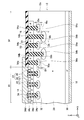
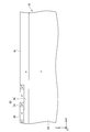
- FIG. 2 is a plan view of the semiconductor device 10.
- FIG. 2 is a longitudinal sectional view taken along line II-II in FIG.
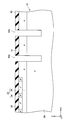
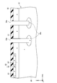
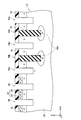
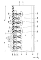
- FIG. 6 is an explanatory diagram of a manufacturing process of the semiconductor device 10.
- FIG. 6 is an explanatory diagram of a manufacturing process of the semiconductor device 10.
- FIG. 6 is an explanatory diagram of a manufacturing process of the semiconductor device 10.
- FIG. 6 is an explanatory diagram of a manufacturing process of the semiconductor device 10.
- FIG. 6 is an explanatory diagram of a manufacturing process of the semiconductor device 10.
- the insulated gate semiconductor device of the embodiment described below is listed. Each of the following features is useful independently.
- the fifth region partially overlaps the sixth region. By disposing the fifth region and the sixth region in this way, these can be disposed closer to each other. Thereby, the breakdown voltage of the insulated gate semiconductor device can be further improved. Further, the manufacturing error at the position in the depth direction of the fifth region and the sixth region is smaller than the manufacturing error at the position in the plane direction. Therefore, even if the fifth region and the sixth region are arranged as described above, they can be prevented from being connected by a manufacturing error.
- the thickness of the sixth region is larger than the thickness of the fifth region.
- the curve of the interface of the sixth region becomes gentler than the curve of the interface of the fifth region.
- the electric field tends to concentrate in the sixth region because it protrudes to the back side of the fifth region.
- the electric field concentration in the sixth region is reduced by making the curve of the interface of the sixth region gentle in this way. can do.
- the second region includes the first type second conductivity type impurity, and the sixth region has a second diffusion coefficient larger in the semiconductor substrate than the first type second conductivity type impurity. Species second conductivity type impurities are included. According to this configuration, the curve of the interface of the sixth region can be made gentle.
- the semiconductor substrate is made of SiC, carbon and boron are included in the fifth region and the sixth region, and the concentration of carbon in the fifth region is higher than the concentration of carbon in the sixth region. . According to this configuration, the curve of the interface of the sixth region can be made gentle.
- a plurality of first outer periphery trenches and second outer periphery trenches are alternately formed in a region outside the second region.
- An insulated gate semiconductor device can be manufactured by the following method.
- the method includes a step of forming a first outer periphery trench, a step of forming a fifth region by implanting a second conductivity type impurity into the bottom surface of the first outer periphery trench, a step of forming a second outer periphery trench, A step of forming a sixth region by injecting a second conductivity type impurity into the bottom surface of the second outer peripheral trench; (Feature 7) Either the first outer periphery trench or the second outer periphery trench is formed first, and after forming the one trench, the bottom surface of the one of the fifth region and the sixth region Forming an exposed region on the bottom surface of the one trench, forming an insulating layer in the one trench, and forming the insulating layer; After forming the other trench of the two outer peripheral trenches and forming the other trench, a region exposed on the bottom surface of the other one of the fifth region and the sixth region is formed, and the other trench After forming the region exposed at the bottom, an insulating layer is formed in the
- the step of forming the sixth region is performed prior to the step of forming the fifth region.
- the second conductivity type impurity is implanted into the bottom surface of the second outer peripheral trench.
- the semiconductor substrate is annealed after implanting the second conductivity type impurity into the bottom surface of the first outer peripheral trench.
- the interface curve of the sixth region can be made gentle.
- the annealing temperature in the step of forming the sixth region is higher than the annealing temperature in the step of forming the fifth region. According to this method, the curve of the interface of the sixth region can be made gentler.
- the first type second conductivity type impurity is implanted into the bottom surface of the first outer periphery trench, and in the step of forming the sixth region, the bottom surface of the second outer periphery trench is formed.
- a second type of second conductivity type impurity having a larger diffusion coefficient in the semiconductor substrate than the first type of second conductivity type impurity is implanted.
- the curve of the interface of the sixth region can be made gentle.
- the semiconductor substrate is made of SiC, and in the step of forming the fifth region, carbon and boron are implanted into the bottom surface of the first outer periphery trench, and in the step of forming the sixth region, the bottom surface of the second outer periphery trench is formed. Inject boron.
- the curve of the interface of the sixth region can be made gentler.
- the gate trench is formed simultaneously with the first outer peripheral trench.
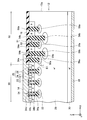
- Example 1 A semiconductor device 10 shown in FIG. 1 has a semiconductor substrate 12 made of SiC.
- the semiconductor substrate 12 has a cell region 20 and an outer peripheral region 50.
- a MOSFET is formed in the cell region 20.
- the outer peripheral region 50 is a region between the cell region 20 and the end surface 12 a of the semiconductor substrate 12.
- a surface electrode 14 and an insulating layer 16 are formed on the surface of the semiconductor substrate 12.
- the insulating layer 16 covers the surface of the semiconductor substrate 12 in the outer peripheral region 50.
- the surface electrode 14 is in contact with the semiconductor substrate 12 in the cell region 20.
- the contact region where the surface electrode 14 is in contact with the semiconductor substrate 12 is the cell region 20, and the region on the outer peripheral side (end face 12 a side) than the contact region is the outer peripheral region 50.
- a back electrode 18 is formed on the back surface of the semiconductor substrate 12. The back electrode 18 covers substantially the entire back surface of the semiconductor substrate 12.
- a source region 22, a body region 23, a drift region 28, a drain region 30, a p-type floating region 32, and a gate trench 34 are formed.
- the source region 22 (an example of a first region in the claims) is an n-type region containing an n-type impurity at a high concentration.
- the source region 22 is formed in a range exposed on the upper surface of the semiconductor substrate 12.
- the source region 22 is in contact with the surface electrode 14 and is ohmically connected to the surface electrode 14.
- the body region 23 (an example of a second region in the claims) has a body contact region 24 and a low concentration region 26.
- the body contact region 24 is a p-type region containing a p-type impurity at a high concentration.
- the body contact region 24 is formed so as to be exposed on the upper surface of the semiconductor substrate 12 at a position where the source region 22 is not formed.
- the body contact region 24 is in contact with the surface electrode 14 and is ohmically connected to the surface electrode 14.
- the low concentration region 26 is a p-type region containing a p-type impurity at a low concentration.
- the p-type impurity concentration of the low concentration region 26 is lower than the p-type impurity concentration of the body contact region 24.
- the low concentration region 26 is formed below the source region 22 and the body contact region 24 and is in contact with these regions.
- the drift region 28 (an example of a third region in the claims) is an n-type region containing an n-type impurity at a low concentration.
- the n-type impurity concentration of the drift region 28 is lower than the n-type impurity concentration of the source region 22.
- the drift region 28 is formed below the body region 23.
- the drift region 28 is in contact with the body region 23 and is separated from the source region 22 by the body region 23.
- the drain region 30 is an n-type region containing an n-type impurity at a high concentration.
- the n-type impurity concentration of the drain region 30 is higher than the n-type impurity concentration of the drift region 28.
- the drain region 30 is formed below the drift region 28.
- the drain region 30 is in contact with the drift region 28 and is separated from the body region 23 by the drift region 28.
- the drain region 30 is formed in a range exposed on the lower surface of the semiconductor substrate 12.
- the drain region 30 is ohmically connected to the back electrode 18.
- each gate trench 34 extends linearly in parallel with each other on the surface of the semiconductor substrate 12. As shown in FIG. 2, each gate trench 34 is formed to penetrate the source region 22 and the body region 23 and reach the drift region 28.
- a bottom insulating layer 34a, a gate insulating film 34b, and a gate electrode 34c are formed in each gate trench 34.
- the bottom insulating layer 34 a is a thick insulating layer formed at the bottom of the gate trench 34.
- a side surface of the gate trench 34 above the bottom insulating layer 34a is covered with a gate insulating film 34b.
- a gate electrode 34c is formed in the gate trench 34 above the bottom insulating layer 34a.
- the gate electrode 34c faces the source region 22, the body region 23, and the drift region 28 through the gate insulating film 34b.
- the gate electrode 34c is insulated from the semiconductor substrate 12 by the gate insulating film 34b and the bottom insulating layer 34a.
- the upper surface of the gate electrode 34c is covered with an insulating layer 34d.
- the gate electrode 34c is insulated from the surface electrode 14 by the insulating layer 34d.
- the p-type floating region 32 (an example of the fourth region of the claims) is formed in the semiconductor substrate 12 in a range exposed to the bottom surface of each gate trench 34 (that is, a range in contact with the bottom surface). Each p-type floating region 32 is surrounded by a drift region 28. The p-type floating regions 32 are separated from each other by the drift region 28. Each p-type floating region 32 is separated from body region 23 by drift region 28.
- a p-type surface region 51 is formed in a range exposed on the surface of the semiconductor substrate 12 in the outer peripheral region 50.
- the surface region 51 extends to substantially the same depth as the body region 23.
- the entire upper surface of the surface region 51 is covered with the insulating layer 16. Therefore, the surface region 51 is not in contact with the surface electrode 14.
- the drift region 28 and the drain region 30 described above extend to the outer peripheral region 50.
- the drift region 28 and the drain region 30 extend to the end face 12 a of the semiconductor substrate 12.
- the drift region 28 is in contact with the surface region 51 from below.
- a plurality of outer peripheral trenches 54 are formed on the upper surface of the semiconductor substrate 12 in the outer peripheral region 50.
- Each outer peripheral trench 54 is formed so as to penetrate the surface region 51 and reach the drift region 28.
- each outer periphery trench 54 is formed in an annular shape that makes a round around the cell region 20 when the semiconductor substrate 12 is viewed from above.
- the surface region 51 is separated from the body region 23 (that is, the p-type region in contact with the source region 22 and the surface electrode 14) by the innermost outer peripheral trench 54. Further, the surface regions 51 are separated from each other by the outer peripheral trenches 54.
- the p-type region inside the innermost outer peripheral trench 54 is the body region 23, and the p-type region outermost than the innermost outer peripheral trench 54 is the surface region 51. Therefore, the outer periphery trench 54 is formed outside the body region 23. An insulating layer 53 is formed in each outer peripheral trench 54.
- the outer peripheral trench 54 includes a first outer peripheral trench 54a and a second outer peripheral trench 54b.
- the depth of the first outer peripheral trench 54 a is substantially equal to the depth of the gate trench 34.
- the second outer peripheral trench 54b is deeper than the first outer peripheral trench 54a.
- the innermost outer peripheral trench 54 is a first outer peripheral trench 54a.
- the first outer peripheral trenches 54a and the second outer peripheral trenches 54b are alternately arranged from the inner peripheral side toward the outer peripheral side.
- a p-type bottom region 56 (that is, 56a and 56b) is formed in the semiconductor substrate 12 and in a range exposed on the bottom surface of each outer peripheral trench 54 (that is, a range in contact with the bottom surface).
- the bottom surface region 56 is formed along the outer periphery trench 54 so as to cover the entire bottom surface of the outer periphery trench 54.
- the periphery of each bottom surface region 56 is surrounded by a drift region 28 (an example of a seventh region in the claims) in the outer peripheral region 50.
- the bottom surface regions 56 are separated from each other by the drift region 28 in the outer peripheral region 50.
- the bottom surface region 56 includes a first bottom surface region 56a (an example of a fifth region in the claims) exposed on the bottom surface of the first outer periphery trench 54a and a second bottom surface region 56b (invention) exposed on the bottom surface of the second outer periphery trench 54b. Of the sixth region).
- the first bottom area 56a is formed at a shallower position than the second bottom area 56b. That is, the lower end 55a of the first bottom surface region 56a is located above the upper end 55b of the second bottom surface region 56b. Therefore, a gap D1 is formed in the depth direction of the semiconductor substrate 12 between the lower end 55a of the first bottom surface region 56a and the upper end 55b of the second bottom surface region 56b.
- the first bottom surface region 56a partially overlaps the adjacent second bottom surface region 56b when the top surface of the semiconductor substrate 12 is viewed in plan (that is, when viewed along the depth direction of the semiconductor substrate 12). Is arranged.
- the first bottom region 56a contains Al (aluminum) as a p-type impurity.
- the second bottom surface region 56b contains B (boron) as a p-type impurity.
- the thickness Db of the second bottom area 56b is larger than the thickness Da of the first bottom area 56a.
- the width Wb of the second bottom surface region 56b (the width in the direction from the inner peripheral side toward the outer peripheral side) is larger than the width Wa of the first bottom surface region 56a.
- the curve of the interface (interface with the drift region 28) of the second bottom surface region 56b is gentler than the curve of the interface (interface with the drift region 28) of the first bottom surface region 56a. That is, the curvature of the interface of the second bottom region 56b is smaller than the curvature of the interface of the first bottom region 56a.
- the operation of the semiconductor device 10 will be described.
- a voltage that makes the back electrode 18 positive is applied between the back electrode 18 and the front electrode 14.
- the MOSFET in the cell region 20 is turned on by applying a gate-on voltage to the gate electrode 34c. That is, a channel is formed in the body region 23 at a position facing the gate electrode 34 c, and from the front surface electrode 14 to the back surface electrode 18 via the source region 22, the channel, the drift region 28, and the drain region 30. Electrons flow.
- the channel disappears and the MOSFET is turned off.
- the MOSFET is turned off, a depletion layer spreads in the drift region 28 from the pn junction at the boundary between the body region 23 and the drift region 28.
- the depletion layer reaches the p-type floating region 32 in the cell region 20, the depletion layer also extends from the p-type floating region 32 into the drift region 28. Therefore, the drift region 28 located between the two p-type floating regions 32 is depleted by the depletion layers extending from the p-type floating regions 32 on both sides.
- the depletion layer extends in the cell region 20, thereby realizing a high breakdown voltage in the cell region 20.
- the depletion layer extending from the above-described pn junction reaches the first bottom surface region 56a below the first outer peripheral trench 54a located closest to the cell region 20 side. Then, a depletion layer spreads from the first bottom surface region 56 a into the surrounding drift region 28. Since the distance between the first bottom surface region 56a and the second bottom surface region 56b adjacent to it (next to the outer peripheral side) is narrow, the depletion layer extending from the first bottom surface region 56a reaches the adjacent second bottom surface region 56b. Then, a depletion layer spreads from the second bottom surface region 56b into the surrounding drift region 28.
- the depletion layer extending from the second bottom surface region 56b reaches the adjacent first bottom surface region 56a.
- the depletion layer extends to the outer peripheral side via the first bottom surface region 56a and the second bottom surface region 56b. In this way, the depletion layer extends from the innermost bottom surface region 56 to the outermost peripheral bottom surface region 56.
- the depletion layer extends widely in the drift region 28 in the outer peripheral region 50.
- the bottom surface regions 56 are separated from each other by the drift region 28. Therefore, a potential difference is generated between the bottom surface regions 56.
- the potential is distributed so that the potential gradually changes from the inner peripheral side toward the outer peripheral side.
- the depletion layer extends in the outer peripheral region 50 and a potential distribution that gradually changes in the outer peripheral region 50 is formed, so that electric field concentration in the outer peripheral region 50 is suppressed. Therefore, the semiconductor device 10 has a high breakdown voltage.
- the second bottom surface region 56b protrudes below the first bottom surface region 56a. For this reason, in the state where the depletion layer spreads in the outer peripheral region 50, the electric field tends to concentrate around the second bottom surface region 56b.
- the thickness Db of the second bottom surface region 56b is thick, and thereby the curve of the interface of the second bottom surface region 56b is loosened.
- the curve of the interface of the 2nd bottom face field 56b has become loose, electric field concentration near the 2nd bottom face field 56b is controlled. Thereby, the breakdown voltage of the semiconductor device 10 is further improved.
- the source region 22, the body region 23, and the surface region 51 are formed in the semiconductor substrate 12 by epitaxial growth, ion implantation, or the like.
- a mask 60 for example, an oxide film having an opening is formed on the surface of the semiconductor substrate 12, and the semiconductor substrate 12 in the opening is etched by anisotropic etching. As a result, the second outer peripheral trench 54b is formed.
- B boron: an example of the second conductivity type impurity of the second type of claims
- the semiconductor substrate 12 is annealed (first annealing).
- the implanted B is activated and diffused.
- the second bottom surface region 56b is formed.
- an insulating layer 53 is formed in the second outer peripheral trench 54b by growing an insulator in the second outer peripheral trench 54b.
- a mask 62 for example, an oxide film having an opening is formed on the surface of the semiconductor substrate 12, and the semiconductor substrate 12 in the opening is etched by anisotropic etching. Thereby, the first outer peripheral trench 54a and the gate trench 34 are formed.
- the first outer peripheral trench 54a and the gate trench 34 are formed shallower than the second outer peripheral trench 54b.
- the first outer peripheral trench 54a is formed next to the second outer peripheral trench 54b so that the first outer peripheral trench 54a and the second outer peripheral trench 54b are alternately arranged.
- Al (aluminum: an example of the first type second conductivity type impurity in the claims) is implanted into the bottom surface of the first outer peripheral trench 54a and the bottom surface of the gate trench 34, and then the semiconductor substrate 12 is annealed (second Anneal).
- the second annealing is performed at a lower temperature than the first annealing. This activates and diffuses the implanted Al. Thereby, as shown in FIG. 7, the first bottom region 56a and the p-type floating region 32 are formed.
- an insulator is grown inside the first outer peripheral trench 54 a and the gate trench 34. Thereby, the insulating layer 53 is formed in the first outer periphery trench 54a. Next, the insulator in the gate trench 34 is partially removed, and then a gate insulating film 34 b and a gate electrode 34 c are formed in the gate trench 34.
- the structure on the upper surface side of the semiconductor device 10 is completed by forming the insulating layer 34d, the insulating layer 16, and the surface electrode 14 on the upper surface of the semiconductor substrate 12.
- the structure on the lower surface side of the semiconductor substrate 12 that is, the drain region 30 and the back electrode 18 is formed. Thereby, the semiconductor device 10 of FIGS. 1 and 2 is completed.
- the relative positions of the first outer peripheral trench 54a and the second outer peripheral trench 54b are likely to shift in the direction along the upper surface of the semiconductor substrate 12 (that is, the X direction and the Y direction). That is, the errors in the X direction and the Y direction at the positions of the first outer peripheral trench 54a and the second outer peripheral trench 54b are large. In particular, in the above embodiment, this error is larger because the first outer periphery trench 54a and the second outer periphery trench 54b are formed in separate steps.
- the position of the first bottom surface region 56a in the X direction and the Y direction varies depending on the position of the first outer peripheral trench 54a, and the position of the second bottom surface region 56b in the X direction and Y direction varies depending on the position of the second outer peripheral trench 54b. For this reason, the relative positions of the first bottom surface region 56a and the second bottom surface region 56b are likely to shift in the X direction and the Y direction. However, in the semiconductor device 10, the positions of the first bottom surface region 56 a and the second bottom surface region 56 b are different in the thickness direction (that is, the Z direction) of the semiconductor substrate 12. More specifically, a space D1 is formed between the first bottom surface region 56a and the second bottom surface region 56b.
- the first bottom surface region 56a and the second bottom surface region 56b are greatly shifted in the X direction or the Y direction.
- the first bottom surface region 56a and the second bottom surface region 56b are not connected.
- the first bottom surface region 56a is not connected to the second bottom surface region 56b.
- the position of the first bottom region 56a in the Z direction varies depending on the depth of the first outer peripheral trench 54a and the impurity implantation range and diffusion range with respect to the first bottom region 56a.
- the position of the second bottom surface region 56b in the Z direction varies depending on the depth of the second outer peripheral trench 54b and the impurity implantation range and diffusion range for the second bottom surface region 56b.
- the depth of each trench and the impurity implantation and diffusion ranges can be accurately controlled. For this reason, the position of the 1st bottom face area
- the distance D1 between the first bottom surface region 56a and the second bottom surface region 56b in the Z direction can be accurately controlled. For this reason, the interval D1 can be shortened. For this reason, according to said manufacturing method, the proof pressure of the outer peripheral area
- Al is implanted as the p-type impurity of the first bottom region 56a
- B is implanted as the p-type impurity of the second bottom region 56b.
- the diffusion coefficient of B in the semiconductor substrate 12 that is, SiC
- the second bottom surface region 56b can be made larger than the first bottom surface region 56a.
- the first annealing is performed at a higher temperature than the second annealing. For this reason, the diffusion distance of B becomes larger in the first annealing. Also by this, the 2nd bottom face area
- the second bottom surface region 56b is formed before the first bottom surface region 56a. For this reason, the second bottom surface region 56b is heated not only by the first annealing but also by the second annealing. In the second annealing, B in the second bottom region 56b is further diffused, so that the second bottom region 56b is enlarged. Also by this, the 2nd bottom face area
- the thickness Db of the second bottom surface region 56b is larger than the thickness Da of the first bottom surface region 56a.
- the interface curve of the second bottom region 56b becomes gentler than the interface curve of the first bottom region 56a. Since the second bottom surface region 56b is formed in this way, as described above, electric field concentration in the vicinity of the second bottom surface region 56b can be suppressed when the MOSFET is turned off.
- the semiconductor device 10 can be reduced in size by reducing the size of the first bottom surface region 56a.
- the first outer peripheral trench 54a and the second outer peripheral trench 54b are formed in separate steps. If the first outer peripheral trench 54a and the second outer peripheral trench 54b are formed at the same time, cracks are likely to occur in the thin partition (semiconductor layer) between the first outer peripheral trench 54a and the second outer peripheral trench 54b.
- the second outer periphery trench 54b is formed as described above, and then the first outer periphery trench 54a is formed after the insulating layer 53 is buried in the second outer periphery trench 54b, a thin partition wall is not formed, and thus cracks are generated. Can be suppressed. Even if the first outer periphery trench 54a is formed first and the second outer periphery trench 54b is formed after the insulating layer 53 is buried in the first outer periphery trench 54a, the problem of partition wall cracks can be solved.
- Example 2 In the semiconductor device of Example 2, both the p-type impurity contained in the first bottom surface region 56a and the p-type impurity contained in the second bottom surface region 56b are B. In addition, the concentration of C (carbon) in the first bottom surface region 56a is higher than the concentration of C in the second bottom surface region 56b.
- Other configurations of the semiconductor device of the second embodiment are the same as those of the semiconductor device 10 of the first embodiment. For this reason, the semiconductor device of the second embodiment also operates in the same manner as the semiconductor device 10 of the first embodiment.
- a method for manufacturing the semiconductor device of Example 2 will be described. First, the structure shown in FIG. 6 is formed in the same manner as in the first embodiment. Next, C is implanted into the bottom surface of the first outer periphery trench 54a. As a result, the concentration of C in the vicinity of the bottom surface of the first outer periphery trench 54a increases. Next, B is implanted into the bottom surface of the first outer peripheral trench 54a. That is, here, C and B are co-doped on the bottom surface of the first outer periphery trench 54a. Next, the semiconductor substrate 12 is annealed (second anneal). Thereby, B implanted into the semiconductor substrate 12 is activated and diffused. As a result, as shown in FIG. 7, a first bottom surface region 56a is formed. In the manufacturing method of the second embodiment, the p-type floating region 32 may be formed simultaneously with the first bottom surface region 56a. Thereafter, the semiconductor device of Example 2 is completed in the same manner as the method of Example 1.
- the diffusion coefficient of B in the semiconductor substrate 12 becomes small. That is, B becomes difficult to diffuse. Therefore, according to the manufacturing method of the second embodiment, the small first bottom region 56a can be formed.
- the second second bottom region 56b is large in the manufacturing method of the second embodiment as in the manufacturing method of the first embodiment. Is formed. Therefore, as shown in FIG. 2, the second bottom surface region 56b can be made larger than the first bottom surface region 56a even in the manufacturing method of the second embodiment.
- the temperature of the second annealing may be higher than the temperature of the first annealing, similarly to the manufacturing method of the first embodiment.
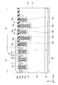
- the outermost peripheral trench 54 on the innermost peripheral side was the first outer peripheral trench 54a.
- the innermost outer peripheral trench 54 may be a second outer peripheral trench 54b (deep trench).
- the gate trench 34 and the outermost peripheral trench 54 on the innermost side have substantially the same depth.
- the innermost outer peripheral trench 54 may be deeper than the gate trench 34 or shallower than the gate trench 34.
- first outer periphery trenches 54a and second outer periphery trenches 54b are alternately formed.
- two first outer peripheral trenches 54a may be formed side by side, or two second outer peripheral trenches 54b may be formed side by side.
- the 1st outer periphery trench 54a and the 2nd outer periphery trench 54b may be formed in the outer periphery area
- the second bottom surface region 56b is thicker than the first bottom surface region 56a.
- the thickness of the second bottom region 56b may be equal to or less than the thickness of the first bottom region 56a.
- the first bottom surface region 56a and the second bottom surface region 56b partially overlap. However, as shown in FIG. 10, these do not need to overlap. Even in such a configuration, it is possible to prevent the first bottom surface region 56a and the second bottom surface region 56b from being connected by an error in the position in the X direction or the Y direction. Further, even if the first bottom surface region 56a and the second bottom surface region 56b do not overlap, the depletion is from the first bottom surface region 56a to the second bottom surface region 56b (or from the second bottom surface region 56a to the first bottom surface region 56b). It is possible to stretch the layer.
- the semiconductor substrate 12 is made of SiC.
- a semiconductor substrate made of another material such as Si may be used.
- a p-type region connected to a predetermined potential may be formed instead of the p-type floating region 32 of the above-described embodiment.
Landscapes
- Engineering & Computer Science (AREA)
- Physics & Mathematics (AREA)
- Condensed Matter Physics & Semiconductors (AREA)
- General Physics & Mathematics (AREA)
- Manufacturing & Machinery (AREA)
- Computer Hardware Design (AREA)
- Microelectronics & Electronic Packaging (AREA)
- Power Engineering (AREA)
- Chemical & Material Sciences (AREA)
- Crystallography & Structural Chemistry (AREA)
- Electrodes Of Semiconductors (AREA)
Priority Applications (4)
| Application Number | Priority Date | Filing Date | Title |
|---|---|---|---|
| DE112015001756.9T DE112015001756B4 (de) | 2014-04-09 | 2015-02-10 | Halbleitervorrichtung mit isoliertem Gate und Verfahren zur Herstellung der Halbleitervorrichtung mit isoliertem Gate |
| CN201580018795.1A CN106463523B (zh) | 2014-04-09 | 2015-02-10 | 绝缘栅型半导体装置、以及绝缘栅型半导体装置的制造方法 |
| US15/124,920 US9755042B2 (en) | 2014-04-09 | 2015-02-10 | Insulated gate semiconductor device and method for manufacturing the insulated gate semiconductor device |
| KR1020167030658A KR101887795B1 (ko) | 2014-04-09 | 2015-02-10 | 절연 게이트형 반도체 장치, 및 절연 게이트형 반도체 장치의 제조 방법 |
Applications Claiming Priority (2)
| Application Number | Priority Date | Filing Date | Title |
|---|---|---|---|
| JP2014080040A JP6208612B2 (ja) | 2014-04-09 | 2014-04-09 | 絶縁ゲート型半導体装置、及び、絶縁ゲート型半導体装置の製造方法 |
| JP2014-080040 | 2014-04-09 |
Publications (1)
| Publication Number | Publication Date |
|---|---|
| WO2015156023A1 true WO2015156023A1 (ja) | 2015-10-15 |
Family
ID=54287604
Family Applications (1)
| Application Number | Title | Priority Date | Filing Date |
|---|---|---|---|
| PCT/JP2015/053692 WO2015156023A1 (ja) | 2014-04-09 | 2015-02-10 | 絶縁ゲート型半導体装置、及び、絶縁ゲート型半導体装置の製造方法 |
Country Status (6)
Families Citing this family (10)
| Publication number | Priority date | Publication date | Assignee | Title |
|---|---|---|---|---|
| JP6266975B2 (ja) | 2013-12-26 | 2018-01-24 | トヨタ自動車株式会社 | 絶縁ゲート型半導体装置の製造方法及び絶縁ゲート型半導体装置 |
| JP6278048B2 (ja) * | 2016-02-19 | 2018-02-14 | トヨタ自動車株式会社 | 半導体装置 |
| DK201670595A1 (en) * | 2016-06-11 | 2018-01-22 | Apple Inc | Configuring context-specific user interfaces |
| DE112018001179T5 (de) * | 2017-03-06 | 2019-12-24 | Mitsubishi Electric Corporation | Siliciumcarbid-halbleitereinheit, leistungswandler, verfahren zur herstellung einer siliciumcarbid-halbleitereinheit und verfahren zur herstellung eines leistungswandlers |
| JP2019046991A (ja) * | 2017-09-04 | 2019-03-22 | ルネサスエレクトロニクス株式会社 | 半導体装置およびその製造方法 |
| CN107634095A (zh) * | 2017-09-14 | 2018-01-26 | 全球能源互联网研究院 | 沟槽型半导体功率器件及其制备方法 |
| CN109300977A (zh) * | 2018-10-08 | 2019-02-01 | 深圳市南硕明泰科技有限公司 | 一种晶体管及其制作方法 |
| DE102019119121B3 (de) | 2019-07-15 | 2020-09-03 | Infineon Technologies Ag | Graben-kontaktstruktur enthaltende halbleitervorrichtung und herstellungsverfahren |
| JP7326991B2 (ja) * | 2019-08-22 | 2023-08-16 | 株式会社デンソー | スイッチング素子 |
| JP7288827B2 (ja) * | 2019-09-06 | 2023-06-08 | ルネサスエレクトロニクス株式会社 | 半導体装置の製造方法 |
Citations (6)
| Publication number | Priority date | Publication date | Assignee | Title |
|---|---|---|---|---|
| JP2005223349A (ja) * | 2005-03-11 | 2005-08-18 | Kansai Electric Power Co Inc:The | 高耐圧半導体装置及びこれを用いた電力変換器 |
| JP2006128507A (ja) * | 2004-10-29 | 2006-05-18 | Toyota Motor Corp | 絶縁ゲート型半導体装置およびその製造方法 |
| JP2007173319A (ja) * | 2005-12-19 | 2007-07-05 | Toyota Motor Corp | 絶縁ゲート型半導体装置およびその製造方法 |
| JP2008103683A (ja) * | 2006-08-03 | 2008-05-01 | Infineon Technologies Austria Ag | 省スペース型のエッジ構造を有する半導体素子 |
| JP2010062361A (ja) * | 2008-09-04 | 2010-03-18 | Toyota Motor Corp | 半導体装置 |
| JP2012238741A (ja) * | 2011-05-12 | 2012-12-06 | Panasonic Corp | 半導体装置及びその製造方法 |
Family Cites Families (14)
| Publication number | Priority date | Publication date | Assignee | Title |
|---|---|---|---|---|
| DE4445553A1 (de) * | 1993-12-21 | 1995-06-22 | Nippon Denso Co | Halbleiterbeschleunigungssensor |
| JPH1187698A (ja) | 1997-09-02 | 1999-03-30 | Kansai Electric Power Co Inc:The | 高耐圧半導体装置及びこの装置を用いた電力変換器 |
| US6380569B1 (en) | 1999-08-10 | 2002-04-30 | Rockwell Science Center, Llc | High power unipolar FET switch |
| TW594946B (en) | 2002-01-16 | 2004-06-21 | Sanken Electric Co Ltd | Manufacturing method of semiconductor device |
| JP4538211B2 (ja) * | 2003-10-08 | 2010-09-08 | トヨタ自動車株式会社 | 絶縁ゲート型半導体装置およびその製造方法 |
| JP4453671B2 (ja) | 2006-03-08 | 2010-04-21 | トヨタ自動車株式会社 | 絶縁ゲート型半導体装置およびその製造方法 |
| JP4915221B2 (ja) | 2006-11-28 | 2012-04-11 | トヨタ自動車株式会社 | 半導体装置 |
| US8354711B2 (en) | 2010-01-11 | 2013-01-15 | Maxpower Semiconductor, Inc. | Power MOSFET and its edge termination |
| JP6037499B2 (ja) | 2011-06-08 | 2016-12-07 | ローム株式会社 | 半導体装置およびその製造方法 |
| US20140221427A1 (en) | 2011-06-22 | 2014-08-07 | Celgene Corporation | Isotopologues of pomalidomide |
| US20130087852A1 (en) | 2011-10-06 | 2013-04-11 | Suku Kim | Edge termination structure for power semiconductor devices |
| US8653587B2 (en) | 2012-02-13 | 2014-02-18 | Force Mos Technology Co., Ltd. | Trench MOSFET having a top side drain |
| JP6139355B2 (ja) | 2013-09-24 | 2017-05-31 | トヨタ自動車株式会社 | 半導体装置 |
| JP6266975B2 (ja) | 2013-12-26 | 2018-01-24 | トヨタ自動車株式会社 | 絶縁ゲート型半導体装置の製造方法及び絶縁ゲート型半導体装置 |
-
2014
- 2014-04-09 JP JP2014080040A patent/JP6208612B2/ja not_active Expired - Fee Related
-
2015
- 2015-02-10 CN CN201580018795.1A patent/CN106463523B/zh active Active
- 2015-02-10 DE DE112015001756.9T patent/DE112015001756B4/de active Active
- 2015-02-10 KR KR1020167030658A patent/KR101887795B1/ko not_active Expired - Fee Related
- 2015-02-10 US US15/124,920 patent/US9755042B2/en active Active
- 2015-02-10 WO PCT/JP2015/053692 patent/WO2015156023A1/ja active Application Filing
Patent Citations (6)
| Publication number | Priority date | Publication date | Assignee | Title |
|---|---|---|---|---|
| JP2006128507A (ja) * | 2004-10-29 | 2006-05-18 | Toyota Motor Corp | 絶縁ゲート型半導体装置およびその製造方法 |
| JP2005223349A (ja) * | 2005-03-11 | 2005-08-18 | Kansai Electric Power Co Inc:The | 高耐圧半導体装置及びこれを用いた電力変換器 |
| JP2007173319A (ja) * | 2005-12-19 | 2007-07-05 | Toyota Motor Corp | 絶縁ゲート型半導体装置およびその製造方法 |
| JP2008103683A (ja) * | 2006-08-03 | 2008-05-01 | Infineon Technologies Austria Ag | 省スペース型のエッジ構造を有する半導体素子 |
| JP2010062361A (ja) * | 2008-09-04 | 2010-03-18 | Toyota Motor Corp | 半導体装置 |
| JP2012238741A (ja) * | 2011-05-12 | 2012-12-06 | Panasonic Corp | 半導体装置及びその製造方法 |
Also Published As
| Publication number | Publication date |
|---|---|
| CN106463523B (zh) | 2019-05-10 |
| KR20160138294A (ko) | 2016-12-02 |
| CN106463523A (zh) | 2017-02-22 |
| JP2015201559A (ja) | 2015-11-12 |
| US9755042B2 (en) | 2017-09-05 |
| US20170025516A1 (en) | 2017-01-26 |
| DE112015001756T5 (de) | 2017-01-19 |
| DE112015001756B4 (de) | 2019-04-04 |
| KR101887795B1 (ko) | 2018-08-10 |
| JP6208612B2 (ja) | 2017-10-04 |
Similar Documents
| Publication | Publication Date | Title |
|---|---|---|
| JP6208612B2 (ja) | 絶縁ゲート型半導体装置、及び、絶縁ゲート型半導体装置の製造方法 | |
| JP6231422B2 (ja) | 半導体装置 | |
| JP6231396B2 (ja) | 半導体装置及び半導体装置の製造方法 | |
| JP6169966B2 (ja) | 半導体装置及び半導体装置の製造方法 | |
| US9780205B2 (en) | Insulated gate type semiconductor device having floating regions at bottom of trenches in cell region and circumferential region and manufacturing method thereof | |
| JP5136578B2 (ja) | 半導体装置 | |
| WO2014115280A1 (ja) | 半導体装置及び半導体装置の製造方法 | |
| JP6571467B2 (ja) | 絶縁ゲート型スイッチング素子とその製造方法 | |
| KR20160018322A (ko) | 반도체 장치의 제조 방법 | |
| JP6104743B2 (ja) | ショットキーダイオードを内蔵するfet | |
| JP5842896B2 (ja) | 半導体装置 | |
| CN104838501B (zh) | 具有超结构造的纵型mosfet的半导体装置及其制造方法 | |
| JP7006389B2 (ja) | 半導体装置および半導体装置の製造方法 | |
| JP2020077824A (ja) | 半導体装置の製造方法 | |
| JP2020057635A (ja) | 半導体装置の製造方法 | |
| JP2024098295A (ja) | 半導体装置の製造方法 | |
| JP2017220644A (ja) | 半導体装置 | |
| JP2020096083A (ja) | トレンチゲート型のスイッチング素子の製造方法 | |
| KR20120069416A (ko) | 절연형 게이트 바이폴라 트랜지스터 및 그 제조 방법 |
Legal Events
| Date | Code | Title | Description |
|---|---|---|---|
| 121 | Ep: the epo has been informed by wipo that ep was designated in this application |
Ref document number: 15776713 Country of ref document: EP Kind code of ref document: A1 |
|
| WWE | Wipo information: entry into national phase |
Ref document number: 15124920 Country of ref document: US |
|
| WWE | Wipo information: entry into national phase |
Ref document number: 112015001756 Country of ref document: DE |
|
| ENP | Entry into the national phase |
Ref document number: 20167030658 Country of ref document: KR Kind code of ref document: A |
|
| 122 | Ep: pct application non-entry in european phase |
Ref document number: 15776713 Country of ref document: EP Kind code of ref document: A1 |