WO2015156016A1 - マスクブランクス、位相シフトマスク及びその製造方法 - Google Patents
マスクブランクス、位相シフトマスク及びその製造方法 Download PDFInfo
- Publication number
- WO2015156016A1 WO2015156016A1 PCT/JP2015/052495 JP2015052495W WO2015156016A1 WO 2015156016 A1 WO2015156016 A1 WO 2015156016A1 JP 2015052495 W JP2015052495 W JP 2015052495W WO 2015156016 A1 WO2015156016 A1 WO 2015156016A1
- Authority
- WO
- WIPO (PCT)
- Prior art keywords
- pattern film
- layer
- light shielding
- film
- mask
- Prior art date
Links
- 230000010363 phase shift Effects 0.000 title claims abstract description 108
- 238000004519 manufacturing process Methods 0.000 title claims abstract description 25
- 239000007769 metal material Substances 0.000 claims abstract description 45
- 239000000758 substrate Substances 0.000 claims abstract description 43
- 230000003287 optical effect Effects 0.000 claims abstract description 39
- 229910052723 transition metal Inorganic materials 0.000 claims abstract description 16
- 150000003624 transition metals Chemical class 0.000 claims abstract description 16
- 239000011651 chromium Substances 0.000 claims description 58
- 239000000463 material Substances 0.000 claims description 58
- 238000005530 etching Methods 0.000 claims description 50
- 239000010703 silicon Substances 0.000 claims description 44
- 229910052710 silicon Inorganic materials 0.000 claims description 44
- 238000002834 transmittance Methods 0.000 claims description 43
- VYZAMTAEIAYCRO-UHFFFAOYSA-N Chromium Chemical compound [Cr] VYZAMTAEIAYCRO-UHFFFAOYSA-N 0.000 claims description 39
- 229910052804 chromium Inorganic materials 0.000 claims description 38
- 238000001312 dry etching Methods 0.000 claims description 25
- YCKRFDGAMUMZLT-UHFFFAOYSA-N Fluorine atom Chemical compound [F] YCKRFDGAMUMZLT-UHFFFAOYSA-N 0.000 claims description 18
- 229910052731 fluorine Inorganic materials 0.000 claims description 18
- 239000011737 fluorine Substances 0.000 claims description 18
- 230000008033 biological extinction Effects 0.000 claims description 17
- 238000010030 laminating Methods 0.000 claims description 4
- 238000005516 engineering process Methods 0.000 abstract description 15
- 238000001459 lithography Methods 0.000 abstract description 7
- 239000000126 substance Substances 0.000 abstract description 6
- 230000000903 blocking effect Effects 0.000 abstract 7
- 239000010410 layer Substances 0.000 description 440
- 239000007789 gas Substances 0.000 description 44
- 229910021344 molybdenum silicide Inorganic materials 0.000 description 44
- XUIMIQQOPSSXEZ-UHFFFAOYSA-N Silicon Chemical compound [Si] XUIMIQQOPSSXEZ-UHFFFAOYSA-N 0.000 description 41
- 230000005672 electromagnetic field Effects 0.000 description 40
- YXTPWUNVHCYOSP-UHFFFAOYSA-N bis($l^{2}-silanylidene)molybdenum Chemical compound [Si]=[Mo]=[Si] YXTPWUNVHCYOSP-UHFFFAOYSA-N 0.000 description 38
- 238000000034 method Methods 0.000 description 36
- 230000000694 effects Effects 0.000 description 21
- QVGXLLKOCUKJST-UHFFFAOYSA-N atomic oxygen Chemical compound [O] QVGXLLKOCUKJST-UHFFFAOYSA-N 0.000 description 19
- 239000001301 oxygen Substances 0.000 description 19
- IJGRMHOSHXDMSA-UHFFFAOYSA-N Atomic nitrogen Chemical compound N#N IJGRMHOSHXDMSA-UHFFFAOYSA-N 0.000 description 18
- 238000005286 illumination Methods 0.000 description 18
- 229910052760 oxygen Inorganic materials 0.000 description 18
- 230000000052 comparative effect Effects 0.000 description 17
- 229910052581 Si3N4 Inorganic materials 0.000 description 14
- HQVNEWCFYHHQES-UHFFFAOYSA-N silicon nitride Chemical group N12[Si]34N5[Si]62N3[Si]51N64 HQVNEWCFYHHQES-UHFFFAOYSA-N 0.000 description 14
- VZSRBBMJRBPUNF-UHFFFAOYSA-N 2-(2,3-dihydro-1H-inden-2-ylamino)-N-[3-oxo-3-(2,4,6,7-tetrahydrotriazolo[4,5-c]pyridin-5-yl)propyl]pyrimidine-5-carboxamide Chemical compound C1C(CC2=CC=CC=C12)NC1=NC=C(C=N1)C(=O)NCCC(N1CC2=C(CC1)NN=N2)=O VZSRBBMJRBPUNF-UHFFFAOYSA-N 0.000 description 12
- 239000000203 mixture Substances 0.000 description 12
- ZAMOUSCENKQFHK-UHFFFAOYSA-N Chlorine atom Chemical compound [Cl] ZAMOUSCENKQFHK-UHFFFAOYSA-N 0.000 description 11
- 239000000460 chlorine Substances 0.000 description 11
- 229910052801 chlorine Inorganic materials 0.000 description 11
- XKRFYHLGVUSROY-UHFFFAOYSA-N Argon Chemical compound [Ar] XKRFYHLGVUSROY-UHFFFAOYSA-N 0.000 description 10
- 238000010894 electron beam technology Methods 0.000 description 10
- 239000011295 pitch Substances 0.000 description 10
- 230000008569 process Effects 0.000 description 10
- ZOKXTWBITQBERF-UHFFFAOYSA-N Molybdenum Chemical compound [Mo] ZOKXTWBITQBERF-UHFFFAOYSA-N 0.000 description 9
- 210000001747 pupil Anatomy 0.000 description 9
- 230000015572 biosynthetic process Effects 0.000 description 8
- 238000009792 diffusion process Methods 0.000 description 8
- 239000011733 molybdenum Substances 0.000 description 8
- 229910052750 molybdenum Inorganic materials 0.000 description 8
- 229910052757 nitrogen Inorganic materials 0.000 description 8
- 238000004088 simulation Methods 0.000 description 8
- 238000012546 transfer Methods 0.000 description 8
- -1 for example Chemical compound 0.000 description 7
- 238000004140 cleaning Methods 0.000 description 6
- 238000011161 development Methods 0.000 description 6
- 238000000206 photolithography Methods 0.000 description 6
- 238000012545 processing Methods 0.000 description 6
- 239000004065 semiconductor Substances 0.000 description 6
- NIPNSKYNPDTRPC-UHFFFAOYSA-N N-[2-oxo-2-(2,4,6,7-tetrahydrotriazolo[4,5-c]pyridin-5-yl)ethyl]-2-[[3-(trifluoromethoxy)phenyl]methylamino]pyrimidine-5-carboxamide Chemical compound O=C(CNC(=O)C=1C=NC(=NC=1)NCC1=CC(=CC=C1)OC(F)(F)F)N1CC2=C(CC1)NN=N2 NIPNSKYNPDTRPC-UHFFFAOYSA-N 0.000 description 5
- VYPSYNLAJGMNEJ-UHFFFAOYSA-N Silicium dioxide Chemical compound O=[Si]=O VYPSYNLAJGMNEJ-UHFFFAOYSA-N 0.000 description 5
- 229910052786 argon Inorganic materials 0.000 description 5
- 150000001875 compounds Chemical class 0.000 description 5
- 238000012937 correction Methods 0.000 description 5
- 238000011156 evaluation Methods 0.000 description 5
- 238000005546 reactive sputtering Methods 0.000 description 5
- 239000012535 impurity Substances 0.000 description 4
- 238000005259 measurement Methods 0.000 description 4
- 239000002356 single layer Substances 0.000 description 4
- 238000004544 sputter deposition Methods 0.000 description 4
- AFCARXCZXQIEQB-UHFFFAOYSA-N N-[3-oxo-3-(2,4,6,7-tetrahydrotriazolo[4,5-c]pyridin-5-yl)propyl]-2-[[3-(trifluoromethoxy)phenyl]methylamino]pyrimidine-5-carboxamide Chemical compound O=C(CCNC(=O)C=1C=NC(=NC=1)NCC1=CC(=CC=C1)OC(F)(F)F)N1CC2=C(CC1)NN=N2 AFCARXCZXQIEQB-UHFFFAOYSA-N 0.000 description 3
- 238000004380 ashing Methods 0.000 description 3
- 238000010586 diagram Methods 0.000 description 3
- 229910052751 metal Inorganic materials 0.000 description 3
- 239000002184 metal Substances 0.000 description 3
- 239000010453 quartz Substances 0.000 description 3
- 229910052715 tantalum Inorganic materials 0.000 description 3
- GUVRBAGPIYLISA-UHFFFAOYSA-N tantalum atom Chemical compound [Ta] GUVRBAGPIYLISA-UHFFFAOYSA-N 0.000 description 3
- HMUNWXXNJPVALC-UHFFFAOYSA-N 1-[4-[2-(2,3-dihydro-1H-inden-2-ylamino)pyrimidin-5-yl]piperazin-1-yl]-2-(2,4,6,7-tetrahydrotriazolo[4,5-c]pyridin-5-yl)ethanone Chemical compound C1C(CC2=CC=CC=C12)NC1=NC=C(C=N1)N1CCN(CC1)C(CN1CC2=C(CC1)NN=N2)=O HMUNWXXNJPVALC-UHFFFAOYSA-N 0.000 description 2
- LDXJRKWFNNFDSA-UHFFFAOYSA-N 2-(2,4,6,7-tetrahydrotriazolo[4,5-c]pyridin-5-yl)-1-[4-[2-[[3-(trifluoromethoxy)phenyl]methylamino]pyrimidin-5-yl]piperazin-1-yl]ethanone Chemical compound C1CN(CC2=NNN=C21)CC(=O)N3CCN(CC3)C4=CN=C(N=C4)NCC5=CC(=CC=C5)OC(F)(F)F LDXJRKWFNNFDSA-UHFFFAOYSA-N 0.000 description 2
- YLZOPXRUQYQQID-UHFFFAOYSA-N 3-(2,4,6,7-tetrahydrotriazolo[4,5-c]pyridin-5-yl)-1-[4-[2-[[3-(trifluoromethoxy)phenyl]methylamino]pyrimidin-5-yl]piperazin-1-yl]propan-1-one Chemical compound N1N=NC=2CN(CCC=21)CCC(=O)N1CCN(CC1)C=1C=NC(=NC=1)NCC1=CC(=CC=C1)OC(F)(F)F YLZOPXRUQYQQID-UHFFFAOYSA-N 0.000 description 2
- WUKWITHWXAAZEY-UHFFFAOYSA-L calcium difluoride Chemical compound [F-].[F-].[Ca+2] WUKWITHWXAAZEY-UHFFFAOYSA-L 0.000 description 2
- 230000007547 defect Effects 0.000 description 2
- 238000013461 design Methods 0.000 description 2
- 229910001873 dinitrogen Inorganic materials 0.000 description 2
- 229910001882 dioxygen Inorganic materials 0.000 description 2
- 230000010354 integration Effects 0.000 description 2
- 230000035699 permeability Effects 0.000 description 2
- 230000002265 prevention Effects 0.000 description 2
- 230000002250 progressing effect Effects 0.000 description 2
- ZOXJGFHDIHLPTG-UHFFFAOYSA-N Boron Chemical compound [B] ZOXJGFHDIHLPTG-UHFFFAOYSA-N 0.000 description 1
- OKTJSMMVPCPJKN-UHFFFAOYSA-N Carbon Chemical compound [C] OKTJSMMVPCPJKN-UHFFFAOYSA-N 0.000 description 1
- MYMOFIZGZYHOMD-UHFFFAOYSA-N Dioxygen Chemical compound O=O MYMOFIZGZYHOMD-UHFFFAOYSA-N 0.000 description 1
- 208000035199 Tetraploidy Diseases 0.000 description 1
- 230000004888 barrier function Effects 0.000 description 1
- 230000008901 benefit Effects 0.000 description 1
- 230000005540 biological transmission Effects 0.000 description 1
- 229910052796 boron Inorganic materials 0.000 description 1
- 229910001634 calcium fluoride Inorganic materials 0.000 description 1
- 238000004364 calculation method Methods 0.000 description 1
- 229910052799 carbon Inorganic materials 0.000 description 1
- 239000000470 constituent Substances 0.000 description 1
- 239000013078 crystal Substances 0.000 description 1
- 230000007423 decrease Effects 0.000 description 1
- 239000003085 diluting agent Substances 0.000 description 1
- 238000009826 distribution Methods 0.000 description 1
- 239000010436 fluorite Substances 0.000 description 1
- 239000001307 helium Substances 0.000 description 1
- 229910052734 helium Inorganic materials 0.000 description 1
- SWQJXJOGLNCZEY-UHFFFAOYSA-N helium atom Chemical compound [He] SWQJXJOGLNCZEY-UHFFFAOYSA-N 0.000 description 1
- 239000001257 hydrogen Substances 0.000 description 1
- 229910052739 hydrogen Inorganic materials 0.000 description 1
- 125000004435 hydrogen atom Chemical class [H]* 0.000 description 1
- 238000007654 immersion Methods 0.000 description 1
- 230000006872 improvement Effects 0.000 description 1
- 150000002500 ions Chemical class 0.000 description 1
- 230000005291 magnetic effect Effects 0.000 description 1
- 150000002739 metals Chemical class 0.000 description 1
- 238000012986 modification Methods 0.000 description 1
- 230000004048 modification Effects 0.000 description 1
- 150000004767 nitrides Chemical class 0.000 description 1
- 230000002093 peripheral effect Effects 0.000 description 1
- 230000010287 polarization Effects 0.000 description 1
- 229910021332 silicide Inorganic materials 0.000 description 1
- FVBUAEGBCNSCDD-UHFFFAOYSA-N silicide(4-) Chemical compound [Si-4] FVBUAEGBCNSCDD-UHFFFAOYSA-N 0.000 description 1
- 150000003376 silicon Chemical class 0.000 description 1
- 230000007704 transition Effects 0.000 description 1
- WFKWXMTUELFFGS-UHFFFAOYSA-N tungsten Chemical compound [W] WFKWXMTUELFFGS-UHFFFAOYSA-N 0.000 description 1
- 229910052721 tungsten Inorganic materials 0.000 description 1
- 239000010937 tungsten Substances 0.000 description 1
- 229910052724 xenon Inorganic materials 0.000 description 1
- FHNFHKCVQCLJFQ-UHFFFAOYSA-N xenon atom Chemical compound [Xe] FHNFHKCVQCLJFQ-UHFFFAOYSA-N 0.000 description 1
Images


Classifications
-
- G—PHYSICS
- G03—PHOTOGRAPHY; CINEMATOGRAPHY; ANALOGOUS TECHNIQUES USING WAVES OTHER THAN OPTICAL WAVES; ELECTROGRAPHY; HOLOGRAPHY
- G03F—PHOTOMECHANICAL PRODUCTION OF TEXTURED OR PATTERNED SURFACES, e.g. FOR PRINTING, FOR PROCESSING OF SEMICONDUCTOR DEVICES; MATERIALS THEREFOR; ORIGINALS THEREFOR; APPARATUS SPECIALLY ADAPTED THEREFOR
- G03F1/00—Originals for photomechanical production of textured or patterned surfaces, e.g., masks, photo-masks, reticles; Mask blanks or pellicles therefor; Containers specially adapted therefor; Preparation thereof
- G03F1/26—Phase shift masks [PSM]; PSM blanks; Preparation thereof
- G03F1/32—Attenuating PSM [att-PSM], e.g. halftone PSM or PSM having semi-transparent phase shift portion; Preparation thereof
-
- G—PHYSICS
- G03—PHOTOGRAPHY; CINEMATOGRAPHY; ANALOGOUS TECHNIQUES USING WAVES OTHER THAN OPTICAL WAVES; ELECTROGRAPHY; HOLOGRAPHY
- G03F—PHOTOMECHANICAL PRODUCTION OF TEXTURED OR PATTERNED SURFACES, e.g. FOR PRINTING, FOR PROCESSING OF SEMICONDUCTOR DEVICES; MATERIALS THEREFOR; ORIGINALS THEREFOR; APPARATUS SPECIALLY ADAPTED THEREFOR
- G03F1/00—Originals for photomechanical production of textured or patterned surfaces, e.g., masks, photo-masks, reticles; Mask blanks or pellicles therefor; Containers specially adapted therefor; Preparation thereof
- G03F1/54—Absorbers, e.g. of opaque materials
Definitions
- the present invention relates to a mask blank, a phase shift mask, and a manufacturing method thereof used for manufacturing a semiconductor device, and in particular, when a mask pattern is transferred onto a wafer using a high NA exposure apparatus, a half pitch of the pattern on the wafer
- the present invention relates to a halftone phase shift mask used in lithography technology of 40 nm or more.
- High integration / miniaturization of semiconductor elements has progressed from the 45 nm node of the design rule to the 32 nm node, and the development of semiconductor elements having a node of 22 nm or less is being promoted.
- photolithography is currently performed by using an optical projection exposure apparatus using an ArF excimer laser with an exposure wavelength of 193 nm to transfer a pattern onto a wafer using a photomask.
- Technology is being implemented.
- a high NA exposure technology with a large numerical aperture (NA) of the projection lens a high refractive index medium is interposed between the projection lens and the object to be exposed.
- NA numerical aperture
- RET technique Resolution Enhancement Technique
- a mask pattern is optimized by applying an auxiliary pattern or bias (a correction amount such as a mask line width) to the mask pattern according to the characteristics of the exposure optical system, or a modified illumination method (oblique illumination method).
- auxiliary pattern or bias a correction amount such as a mask line width
- modified illumination method oblique illumination method
- incident illumination method usually, annular illumination using a pupil filter, dipole illumination using a dipole (also referred to as Dipole) pupil filter, and quadrupole (quadrupole: C-quad) are used. Quadrupole illumination using a pupil filter is also used.
- a light shielding film is formed on a transparent substrate with chromium or the like, and a pattern is formed by a light transmitting part and a light shielding part.
- Levenson-type phase shift mask that improves resolution by phase shift effect using light interference along with miniaturization and high accuracy of binary photomask (hereinafter also referred to as binary mask), light transmitting part and half
- phase shift masks such as half-tone phase shift masks configured by transmitting portions and chromeless phase shift masks not provided with a light-shielding layer such as chrome are progressing.
- the halftone phase shift mask has a mask pattern (hereinafter also referred to as a semitransparent pattern film) made of a semitransparent film on a transparent substrate as a normal configuration, and transmits through the semitransparent pattern film.
- the design is such that the phase of the exposure light and the exposure light transmitted through the transparent substrate are reversed.
- the light intensity decreases due to phase inversion at the boundary between the portion where the translucent pattern film is provided (hereinafter also referred to as the mask pattern portion) and the portion where the transparent substrate is exposed.
- the mask pattern portion a compound of molybdenum silicide
- MoSiON molybdenum oxynitride silicide
- the transmissivity of the semitransparent pattern film is conventionally designed to be about 6%.
- the transmissivity of the semitransparent pattern film is conventionally designed to be about 6%.
- a light-shielding portion hereinafter also referred to as a light-shielding pattern film
- the halftone phase shift mask having such a configuration is referred to as a tritone mask.
- the light-shielding pattern film on the semi-transparent pattern film has a higher light-shielding property.
- the light shielding pattern film is thickened, it is necessary to thicken the resist pattern for processing the light shielding pattern film, and it becomes difficult to process a fine pattern.
- the height of the light shielding pattern film and the semi-transparent pattern film becomes high, and the pattern collapse easily occurs during cleaning.
- the line width of the mask pattern on the photomask is smaller than the wavelength 193 nm of the ArF excimer laser exposure light used for lithography.
- an electromagnetic field EMF: Electro
- the light-shielding pattern film made of a molybdenum silicide (MoSi) -based material whose composition is adjusted according to the demand for thinning as described above does not have sufficient chemical resistance in mask cleaning and light resistance in ArF excimer laser exposure.
- the tritone mask using the above-described molybdenum silicide (MoSi) -based material for the light-shielding pattern film has a problem that the quality such as the optical density cannot be stably maintained.
- the present invention has been made in view of the above problems, and by reducing the thickness of the light-shielding pattern film and maintaining sufficient light-shielding performance, it is possible to reduce the thickness of the resist and improve the cleaning resistance. Even when using a semi-transparent pattern film with high transmittance, it is possible to produce a fine pattern, and further, the EMF bias value can be reduced, and the pattern processability, light resistance, and chemical resistance are excellent on the wafer.
- a mask blank according to the first aspect of the present invention is a mask blank used for producing a halftone phase shift mask to which ArF excimer laser exposure light is applied.
- the light-shielding layer is made of a single metal material that does not contain a transition metal, and the thickness of the light-shielding layer is 40 nm or less, the translucent layer,
- the optical density with respect to the exposure light of the laminate obtained by laminating the three layers of the intermediate layer and the light shielding layer is not less than a value that functions as a light shielding region.
- the mask blank according to the second aspect of the present invention is the mask blank according to the first aspect, wherein the laminated body in which the three types of layers of the translucent layer, the intermediate layer, and the light shielding layer are laminated is the exposure layer.
- the optical density for light is adjusted to be 2.8 or higher.
- a mask blank according to a third aspect of the present invention is the mask blank according to the first or second aspect, wherein the transmissivity T of the translucent layer with respect to the exposure light and the film thickness d of the light shielding layer.
- the mask blank according to claim 4 of the present invention is the mask blank according to any one of claims 1 to 3, wherein the light shielding layer has a refractive index n of 1.0 or less, and The extinction coefficient k is composed of a single metal material having a value of 2.0 or more.
- the mask blank according to claim 5 of the present invention is the mask blank according to any one of claims 1 to 4, wherein the single metal material is silicon. It is.
- a mask blank according to a sixth aspect of the present invention is the mask blank according to any one of the first to fifth aspects, wherein the translucent layer is Si x O 1-xy N y ( x and y satisfy 0 ⁇ x ⁇ 1, 0 ⁇ y ⁇ 1, and 0 ⁇ x + y ⁇ 1).
- a mask blank according to a seventh aspect of the present invention is the mask blank according to any one of the first to sixth aspects, wherein the intermediate layer is resistant to dry etching using a fluorine-based gas. It is comprised from the material which has this.
- a mask blank according to an eighth aspect of the present invention is the mask blank according to any one of the first to seventh aspects, wherein the intermediate layer is made of a chromium-based material containing chromium (Cr).
- the film thickness of the intermediate layer is in the range of 2 nm to 5 nm.
- the mask blank according to claim 9 of the present invention is the mask blank according to any one of claims 1 to 8, wherein the mask blank is against dry etching using a fluorine-based gas on the light shielding layer. And a hard mask layer made of a material having resistance.
- a phase shift mask according to a tenth aspect of the present invention is a halftone phase shift mask to which ArF excimer laser exposure light is applied, and is formed on a transparent substrate and the transparent substrate, and the exposure
- the light shielding pattern film is made of a single metal material not containing a transition metal, and the film thickness of the light shielding pattern film is 40 nm or less, and the translucent pattern film, the intermediate pattern film, and the light shielding pattern film
- the laminated body in which the three kinds of films are laminated has an optical density with respect to the exposure light that is not less than a value that functions as a light shielding region.
- a phase shift mask according to an eleventh aspect of the present invention is the phase shift mask according to the tenth aspect, wherein the three types of films of the translucent pattern film, the intermediate pattern film, and the light shielding pattern film are stacked.
- the body is characterized in that the optical density with respect to the exposure light is adjusted to be 2.8 or more.
- a phase shift mask according to a twelfth aspect of the present invention is the phase shift mask according to the tenth or eleventh aspect, wherein the translucent pattern film has a transmittance T with respect to the exposure light and the light shielding pattern film.
- a phase shift mask according to a thirteenth aspect of the present invention is the phase shift mask according to any one of the tenth to twelfth aspects, wherein the light shielding pattern film has a refractive index n of 1.0 or less. And an extinction coefficient k is made of a single metal material of 2.0 or more.
- the phase shift mask according to the fourteenth aspect of the present invention is the phase shift mask according to any one of the tenth to thirteenth aspects, wherein the single metal material is silicon. To do.
- a phase shift mask according to a fifteenth aspect of the present invention is the phase shift mask according to any one of the tenth to fourteenth aspects, wherein the translucent pattern film is Si x O 1-xy.
- the phase shift mask according to a sixteenth aspect of the present invention is the phase shift mask according to any one of the tenth to fifteenth aspects, wherein the intermediate pattern film is used for dry etching using a fluorine-based gas. It is characterized by being comprised from the material which has tolerance with respect to it.
- the phase shift mask according to claim 17 of the present invention is the phase shift mask according to any one of claims 10 to 16, wherein the intermediate pattern film contains chromium (Cr). And the film thickness of the intermediate pattern film is in the range of 2 nm to 5 nm.
- the manufacturing method of the phase shift mask which concerns on invention of Claim 18 of this invention is a transparent substrate, the semi-transparent layer which is formed on the said transparent substrate, and controls the phase and the transmittance
- the said semi-transparent A mask blank comprising: an intermediate layer formed on the layer; and a light shielding layer formed on the intermediate layer, wherein the light shielding layer is made of a single metal material not including a transition metal.
- a phase shift mask manufacturing method comprising: a transparent substrate; a translucent layer formed on the transparent substrate for controlling the phase and transmittance of the exposure light; and the translucent.
- a mask blank comprising: an intermediate layer formed on the layer; and a light shielding layer formed on the intermediate layer, wherein the light shielding layer is made of a single metal material not including a transition metal.
- a light-shielding pattern film having a high light-shielding property against exposure light is provided even if it is thinned, the value of the EMF bias can be reduced, the pattern workability is good, and the chemical resistance and light resistance are improved.
- An excellent halftone phase shift mask suitable for lithography technology with a half pitch on the wafer of 40 nm or more can be obtained.
- FIG. 6 is a schematic plan view of a quadrupole (C-quad) pupil filter used for evaluating the transfer characteristics of a mask in the present invention. It is a figure which shows the value of the EMF bias in each mask structure. It is a cross-sectional schematic diagram of the binary mask for demonstrating an EMF bias.
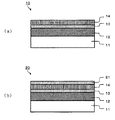
- FIG. 1 is a schematic cross-sectional view showing an example of a mask blank according to the present invention.
- the mask blank 20 in the form shown in FIG. 1B has a hard mask layer 21 on the light shielding layer 14 of the mask blank 10 in the form shown in FIG.
- a mask blank 10 of this embodiment includes a transparent substrate 11, a semitransparent layer 12 formed thereon, and an intermediate layer 13 formed on the semitransparent layer 12. And a light shielding layer 14 formed on the intermediate layer 13.
- the light shielding layer 14 is comprised from the single metal material which does not contain a transition metal, and the film thickness of the light shielding layer 14 is 40 nm or less, 3 types, the semi-transparent layer 12, the intermediate
- the optical density with respect to the ArF excimer laser exposure light of the laminate obtained by laminating these layers is not less than a value functioning as a light shielding region, particularly preferably not less than 2.8.
- the transparent substrate 11, the semi-transparent layer 12, the intermediate layer 13, the light shielding layer 14 and the like constituting the mask blank 10 of the present embodiment will be described.
- Transparent substrate As the transparent substrate 11, optically polished synthetic quartz glass, fluorite, calcium fluoride, or the like that transmits exposure light with high transmittance can be used. Synthetic quartz glass is more preferable because of its stable quality and high transmittance of short wavelength exposure light.
- the translucent layer 12 acts as a halftone layer that controls the phase and transmittance of ArF excimer laser exposure light, and the material thereof is not particularly limited, What has been used for the conventional halftone phase shift mask can be used.
- the translucent layer 12 Si x O 1-xy N y (x and y are 0 ⁇ x ⁇ 1, 0 ⁇ y ⁇ 1, and 0 ⁇ x + y ⁇ ) that is a silicon nitride (SiN) -based material.
- MoSi molybdenum silicide
- MoSiO molybdenum silicide oxide film
- MoSiN molybdenum silicide nitride film
- MoSiON molybdenum silicide oxynitride film
- a film made of Si x O 1-xy N y which is the silicon nitride (SiN) -based material is preferable.
- the translucent layer 12 has a higher transmittance for ArF excimer laser exposure light compared to that used for a conventional halftone phase shift mask including a film made of the molybdenum silicide (MoSi) material. This is because it has transmittance and can be made thinner.
- the film made of Si x O 1-xy N y is not particularly limited, but in particular, the extinction coefficient k at the wavelength of ArF excimer laser exposure light is 0.2 to 0.45.
- the refractive index n at the wavelength of ArF excimer laser exposure light is within the range of 2.3 to 2.7, and the transmittance at the wavelength of ArF excimer laser exposure light is within the range of 15% to 38%.
- n at the wavelength of ArF excimer laser exposure light is within the range of 2.3 to 2.7
- the transmittance at the wavelength of ArF excimer laser exposure light is within the range of 15% to 38%.
- the semitransparent layer 12 can have a higher transmittance and be thinner.
- the phase shift mask formed from the mask blank according to the present invention is used, the light intensity is made zero by the interference of light due to the phase effect at the boundary of the pattern, and the contrast of the transferred image is improved. This is because the phase effect can be made more conspicuous when the translucent layer 12 has a higher light transmittance.
- the film made of Si x O 1-xy N y does not contain a metal, an oxide film of silicon (Si) does not grow even when irradiated with ArF excimer laser exposure light for a long time. This is because it is possible to prevent the pattern dimension (Critical Dimension) from changing. Similarly, the pattern dimension can be prevented from changing in the phase shift mask cleaning process. Therefore, in photolithography, transfer characteristics are excellent, and ArF excimer laser exposure light irradiation resistance and cleaning resistance can be increased.
- the optical density with respect to the ArF excimer laser exposure light of the laminated body in which the three types of layers of the semitransparent layer 12, the intermediate layer 13, and the light shielding layer 14 are laminated is set.
- the total film thickness of the intermediate layer 13 and the light shielding layer 14 required to make the value function as the light shielding region or more, particularly preferably 2.8 or more, is increased. Therefore, in this case, as will be described later, the intermediate layer 13 is made of a chromium-based material containing chromium (Cr), and the light shielding layer 14 is made of silicon (Si) which is a single metal material.
- the intermediate layer 13 by making the intermediate layer 13 thin, the intermediate layer required to make the optical density of the laminate with respect to the ArF excimer laser exposure light greater than a value that functions as a light-shielding region, particularly preferably 2.8 or more.
- the effect of reducing the total film thickness of the light shielding layer 13 and the light shielding layer 14 becomes remarkable because the original film thickness of the entire intermediate layer 13 and light shielding layer 14 is increased.
- the effect of avoiding an increase in the EMF bias value of the phase shift mask becomes significant.
- a film made of Si x O 1-xy N y which is the silicon nitride (SiN) -based material is preferable.
- the intermediate layer 13 is made of a chromium-based material containing chromium (Cr), and the light shielding layer 14 is formed.
- Si silicon
- the translucent layer 12 can be made thinner, and the entire thickness of the intermediate layer 13 and the light shielding layer 14 can be significantly reduced. can do.
- the thickness of the intermediate layer 13 is reduced to 5 nm or less, this effect becomes even more remarkable.
- the film made of Si x O 1-xy N y is not particularly limited, but the nitrogen (N) composition ratio y is in the range of 0.4 to 0.6. Is preferred. This is because if it is less than the above range, it does not reach the above-described desired transmittance range, and if it exceeds the above range, it exceeds the above-described desired transmittance range.
- the film made of Si x O 1-xy N y when oxygen (O) is large, the extinction coefficient k is lowered, so that the transmittance is increased, and as a result, the refractive index n is lowered. This is because the thickness of the film made of Si x O 1-xy N y for obtaining a phase difference of 180 ° is increased.
- the translucent layer 12 is made of, for example, the above silicon nitride (SiN) -based material, a fluorine-based gas such as CF 4 , CHF 3 , C 2 F 6 , a mixed gas thereof, or a gas thereof
- a fluorine-based gas such as CF 4 , CHF 3 , C 2 F 6
- a mixed gas thereof such as CF 4 , CHF 3 , C 2 F 6
- a mixed gas thereof such as an etching gas
- the method for forming the film made of Si x O 1-xy N y is not particularly limited.
- the film made of Si x O 1-xy N y is sputtered. using a target of silicon (Si) for the target, by selecting a sputtering gas as appropriate, the Si x O 1-x-y N Si constituting a film made of y x O 1-x-y N y ( (where x and y satisfy 0 ⁇ x ⁇ 1, 0 ⁇ y ⁇ 1, and 0 ⁇ x + y ⁇ 1)
- the film formation is performed by sputtering under film formation conditions such that a desired ratio is obtained. It is done.
- the thickness of the film made of Si x O 1-xy N y is not particularly limited, but is preferably in the range of 57 nm to 67 nm. If the film thickness is within the range of 57 nm to 67 nm, the film thickness of the semi-transparent layer 12 becomes thinner than that of the conventional semi-transparent layer, so that it becomes easy to form a semi-transparent pattern film by etching. Because. And since the time required for etching is short, as will be described later, it is assumed that the etching barrier layer for preventing the transparent substrate 11 from being damaged was not provided between the transparent substrate 11 and the translucent layer 12. This is because damage to the transparent substrate 11 can be sufficiently avoided when the semitransparent pattern film is formed by etching.
- the film thickness of the Si x O 1-xy N y film is preferably in the range of 57 nm to 64 nm, and particularly preferably in the range of 57 nm to 62 nm.
- the film thickness of the film made of the Si x O 1-x-y N y thinner is, pattern collapse in the semi-transparent pattern layer to be described later are formed from the film made of the Si x O 1-x-y N y This is because the occurrence of defects such as the above can be suppressed, or the processing of the film made of Si x O 1-xy N y and the modification of the translucent pattern film are easy.
- the film thickness of the film made of Si x O 1-xy N y can be calculated by measuring with an ellipsometer VUV-VASE manufactured by JA Woollam.
- the light shielding layer 14 is made of silicon (Si) which is a single metal material
- the above-described film made of molybdenum silicide (MoSi) is used as the semitransparent layer 12.
- MoSi molybdenum silicide
- it is a semi-structure composed of molybdenum silicide (MoSi) -based material as compared with the case where a film made of Si x O 1-xy N y, which is the silicon nitride (SiN) -based material, is used.
- Molybdenum (Mo) is likely to diffuse from the transparent layer 12 to the light shielding layer 14 made of silicon (Si).
- the intermediate layer 13 is diffused between the light-shielding layer 14 made of silicon (Si), which is a single metal material, and the semi-transparent layer 12.
- Si silicon
- the translucent layer 12 is composed of a molybdenum silicide material
- oxygen is added to the fluorine-based gas, for example, CF 4 , CHF 3 , C 2 F 6 , a mixed gas thereof, or a mixed gas thereof.
- the mixed gas as an etching gas, dry etching can be performed to form a pattern.
- the translucent layer used in the conventional halftone phase shift mask is designed so that the transmittance with respect to the exposure light is mainly about 6%.
- the mask blank of the present invention when processed into a phase shift mask, it becomes a form (tritone mask) having a light shielding pattern film on the semitransparent pattern film.
- it can be designed to have a higher transmittance (for example, about 30%).
- the translucent layer 12 has a high transmittance, the phase effect can be further improved.
- the intermediate layer 13 functions as an etching stop layer when etching the light shielding layer 14 and an etching mask when etching the semitransparent layer 12. Further, the intermediate layer 13 functions as a diffusion preventing layer for preventing the material constituting the light shielding layer 14 from diffusing from the light shielding layer 14 to the semitransparent layer 12. As described above, it is preferable to use a silicon nitride (SiN) -based compound or a molybdenum silicide (MoSi) -based compound for the translucent layer 12, and this silicon nitride (SiN) -based compound or molybdenum silicide (MoSi).
- SiN silicon nitride
- MoSi molybdenum silicide
- the intermediate layer 13 may be made of a material having resistance to dry etching using a fluorine-based gas. preferable.
- the material constituting the intermediate layer 13 include chromium-based materials such as Cr, CrO, CrN, and CrNO, and tantalum-based materials such as Ta, TaO, TaN, and TaNO.
- the material constituting the intermediate layer 13 is preferably a chromium-based material containing chromium (Cr) such as Cr, CrO, CrN, or CrNO.
- Cr chromium
- the light shielding layer 14 is made of silicon (Si), which is a single metal material, the materials constituting each layer are prevented from diffusing between the light shielding layer 14 and the translucent layer 12. It is because it can act suitably as a diffusion preventing layer.
- the translucent layer 12 is made of molybdenum silicide compound (MoSi) and the light shielding layer 14 is made of silicon (Si), which is a single metal material, molybdenum ( It is because it can act suitably as a diffusion preventing layer for preventing Mo) from diffusing.
- the intermediate layer 13 can particularly preferably act as a diffusion preventing layer for preventing the materials constituting each layer from diffusing between the light shielding layer 14 and the semitransparent layer 12.
- CrN, CrON, and CrO are preferable.
- the film is formed by reactive sputtering in an atmosphere of nitrogen gas, oxygen gas, or a mixed gas thereof. This is because the stability during film formation is high and the pattern workability is good compared to the chromium film (Cr) to be formed.
- CrN is particularly preferable. This is because since the material does not contain oxygen (O), the film thickness of the CrN film is thinner than the film thickness of the film composed of CrON and CrO.
- the intermediate layer 13 is made thin, and the optical density for the ArF excimer laser exposure light of the laminated body in which the three types of layers of the semitransparent layer 12, the intermediate layer 13, and the light shielding layer 14 are laminated functions as a light shielding region.
- the entire film thickness of the intermediate layer 13 and the light-shielding layer 14 which are required to achieve a value equal to or greater than 2.8, and particularly preferably equal to or greater than 2.8, can be reduced.
- the intermediate layer 13 may have a single layer structure made of the same material or a multilayer structure made of different materials.
- the thickness of the intermediate layer 13 is sufficient to act as an etching stop layer when etching the light shielding layer 14 and an etching mask when etching the semitransparent layer 12, and the light shielding layer.
- the thickness of the phase shift mask is not limited as long as it has a thickness sufficient to act as a diffusion prevention layer for preventing the material constituting the light shielding layer 14 from diffusing from the translucent layer 12 to the semitransparent layer 12. There is a risk that the value of the EMF bias becomes large. Therefore, the film thickness of the intermediate layer 13 is preferably in the range of 2 nm to 5 nm.
- the thickness of the intermediate layer 13 is preferably in the range of 2 nm to 5 nm. If it is less than the above range, since the film thickness is too thin, the intermediate layer 13 cannot be made into a dense film, and since holes are formed in the intermediate layer 13, the translucent layer 12 and the light shielding layer 14 This is because it becomes difficult to prevent the materials constituting each other's layers from diffusing.
- the semitransparent layer 12 is made of molybdenum silicide compound (MoSi) and the light shielding layer 14 is made of silicon (Si) which is a single metal material, the intermediate layer 13 is shielded from the semitransparent layer 12.
- the intermediate layer 13 is made of a chromium-based material containing chromium (Cr) and the light shielding layer 14 is made of silicon (Si) which is a single metal material
- the intermediate layer 13 The effect obtained by reducing the thickness of the film will be described.
- the optical density with respect to the ArF excimer laser exposure light of the laminated body in which the three kinds of layers of the translucent layer 12, the intermediate layer 13, and the light shielding layer 14 are laminated needs to be 2.8 or more.
- a layer composed of silicon (Si), which is a single metal material has a larger extinction coefficient k than a layer composed of a chromium-based material containing chromium (Cr).
- the thickness of the intermediate layer 13 made of a chromium-based material containing chromium (Cr) is reduced, and the ratio of the optical density obtained in the intermediate layer 13 is reduced.
- the optical density of the laminate with respect to ArF excimer laser exposure light is 2.8 or more.
- the intermediate layer 13 For the formation of the intermediate layer 13, a conventionally known vacuum film formation method can be applied.
- the intermediate layer 13 is a chromium film (Cr)
- it is formed by a reactive sputtering method using a chromium target in an argon gas atmosphere. can do.
- the light-shielding layer 14 is comprised from the single metal material which does not contain a transition metal.
- a single metal material film constituting the light shielding layer 14 can be formed by a normal film forming method such as a sputtering method.
- a film of a single metal material can be formed using a target of the single metal material at the time of sputtering, for example, and is composed of a film of a single metal material that is substantially free of other elements.
- the present invention other than the formation of a film of a single metal material, the inclusion of other metals or the formation of oxides or nitrides is not intended, and oxygen or nitrogen gas is not introduced during film formation. .
- the light shielding layer substantially made of the single metal material of the present invention. It is included. That is, in the present invention, “the light shielding layer is composed of a single metal material not including a transition metal” means that the light shielding layer is substantially composed of a single metal material. . Therefore, the “light-shielding layer composed of a single metal material not containing a transition metal” in the present invention may contain impurities that do not affect the function and characteristics of the light-shielding layer. Such impurities are not particularly limited, and examples thereof include carbon, oxygen, nitrogen, boron, helium, hydrogen, argon, and xenon. The ratio of such impurities in the light-shielding layer is not particularly limited, but is preferably 0% or more and 5% or less, more preferably 0% or more and 2% or less, particularly 0 % To 1% is preferable.
- the thickness of the light shielding layer 14 is 40 nm or less, and the optical density of the laminate obtained by laminating three kinds of layers, the semitransparent layer 12, the intermediate layer 13, and the light shielding layer 14, with respect to ArF excimer laser exposure light. Is not less than a value that functions as a light shielding region, particularly preferably not less than 2.8.
- the “light-shielding region” refers to the exposure light transmitted through the semitransparent pattern film in the phase shift mask (halftone type phase shift mask) according to the present invention, which will be described later, formed from the mask blank according to the present invention.
- “functioning as a light shielding region” means exposure light transmitted through a semitransparent pattern film in a phase shift mask (halftone type phase shift mask) according to the present invention, which will be described later, formed from a mask blank according to the present invention. Among them, it means that exposure light unnecessary for transferring the mask pattern to the transfer object is shielded.
- the film thickness of the light shielding layer 14 can be changed within a range satisfying the above optical density. That is, when the translucency of the translucent layer 12 is small, the film thickness of the light shielding layer 14 can be reduced accordingly.
- the light shielding layer 14 is preferably composed of a single metal material having a refractive index n of 1.0 or less and an extinction coefficient k of 2.0 or more. More preferably, the single metal material is silicon (Si). As the extinction coefficient k is higher, the film thickness of the light-shielding layer 14 required to make the optical density of the laminated body with respect to the ArF excimer laser exposure light more than a value that functions as a light-shielding region, particularly preferably 2.8 or more. This is because the thickness can be reduced. This is because it is possible to avoid an increase in the value of the EMF bias of the phase shift mask. Further, silicon (Si) has a high extinction coefficient k among such single metal materials.
- the light shielding layer 14 can be formed by, for example, a reactive sputtering method in an argon (Ar) gas atmosphere using a silicon crystal that does not contain impurity ions as a target.
- examples of the transition metal not included in the light shielding layer include molybdenum (Mo), tantalum (Ta), tungsten (W), and the like, and in particular, transition not including molybdenum (Mo) in the light shielding layer. Listed as metal.
- molybdenum forms silicon and a molybdenum silicide compound (MoSi), and is used, for example, as a light shielding pattern film of a binary photomask.
- the light shielding pattern film using molybdenum silicide (MoSi) -based material does not have sufficient chemical resistance and light resistance, and binary photomasks using molybdenum silicide (MoSi) -based material for the light shielding pattern film are mask-cleaned.
- the mask pattern dimension (CD dimension) changes. Therefore, in the present invention, the light shielding layer is made of a single metal material that does not contain a transition metal such as molybdenum. In a more preferred embodiment, the light shielding layer is made of silicon.
- the light-shielding layer made of silicon shows a faster etching rate than conventional molybdenum silicide light-shielding layers in etching using a fluorine-based gas, and pattern processing is easy, and the resist can be thinned. The resolution can be improved.
- the mask blank according to the present invention may have a hard mask layer 21 on the light shielding layer 14 as in the mask blank 20 of the form shown in FIG.
- the resist can be made thinner.
- the hard mask layer 21 uses a fluorine-based gas. It is preferable to be made of a material having resistance to dry etching. Specific examples of the material constituting the hard mask layer 21 include chromium-based materials such as Cr, CrO, CrN, and CrNO, and tantalum-based materials such as Ta, TaO, TaN, and TaNO.
- the film thickness of the hard mask layer 21 is, for example, in the range of 2 nm to 5 nm.
- the hard mask layer 21 may have a single layer structure made of the same material or a multilayer structure made of different materials.
- a conventionally known vacuum film forming method can be applied.
- the hard mask layer 21 is a chromium film (Cr)
- a reactive sputtering method is performed using a chromium target in an argon gas atmosphere. Can be formed.
- the combination of the intermediate layer 13 and the light shielding layer 14 includes, inter alia, the intermediate layer 13 made of the chromium-based material and silicon (Si) that is the single metal material.
- a combination of the light shielding layers 14 is preferable. This is because silicon (Si), which is the single metal material, has a large extinction coefficient k and a large difference between the extinction coefficients k of the chromium-based material. Accordingly, as described above, it is necessary to make the intermediate layer 13 thin so that the optical density of the laminate with respect to the ArF excimer laser exposure light is not less than a value that functions as a light-shielding region, particularly preferably not less than 2.8. This is because an effect of reducing the total film thickness of the intermediate layer 13 and the light shielding layer 14 can be obtained. This is because this effect becomes significant when the thickness of the intermediate layer 13 is 5 nm or less.
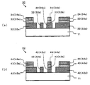
- FIG. 2 is a schematic sectional view showing an example of a phase shift mask according to the present invention.
- the phase shift mask 30 of the present embodiment is formed on the transparent substrate 11, the semitransparent pattern film 32 formed thereon, and the semitransparent pattern film 32.
- the intermediate pattern film 33 and the light shielding pattern film 34 formed on the intermediate pattern film 33 are provided.
- the light shielding pattern film 34 is made of a single metal material that does not contain a transition metal.
- the thickness of the light shielding pattern film 34 is 40 nm or less, and the semitransparent pattern film 32, the intermediate pattern film 33, and the light shielding pattern.
- the optical density with respect to the ArF excimer laser exposure light of the laminate in which the three layers of the film 34 are laminated is not less than a value that functions as a light shielding region, and particularly preferably not less than 2.8.
- the phase shift mask 30 according to the present embodiment can be manufactured from the mask blanks 10 or the mask blanks 20 described above. That is, the translucent pattern film 32 of the phase shift mask 30 can be obtained by processing the translucent layer 12 of the mask blank 10 into a pattern, and similarly, the intermediate pattern film 33 forms the intermediate layer 13 in a pattern.
- the light shielding pattern film 34 can be obtained by processing the light shielding layer 14 into a pattern.
- an intermediate pattern film 33a and a light-shielding pattern film 34a are formed on the semitransparent pattern film 32a at the left end of the phase shift mask 30, and similarly, the phase shift mask At the right end of 30, an intermediate pattern film 33c and a light shielding pattern film 34c are formed on the translucent pattern film 32d.
- the area where the light shielding pattern film 34a and the light shielding pattern film 34c are formed is the outer periphery of the area where the mask pattern is formed (effective area), and the light shielding band is provided in the conventional halftone phase shift mask. This corresponds to the provided area.
- the phase shift mask 30 includes a part (single layer constituent part) composed of only the semitransparent pattern film 32b, a semitransparent pattern film 32c, an intermediate pattern film 33b, and a light shielding pattern film 34b as mask patterns in the effective region. It has a part (laminated structure part) composed of three kinds of films.
- the area of the semi-transparent pattern film 32c of the laminated component is usually larger than the area of the semi-transparent pattern film 32c of the single-layer component. Therefore, the light-shielding pattern film 34b is provided in the laminated component, and the semi-transparent pattern Unnecessary exposure light passing through the film is reliably shielded.
- the phase shift mask 30 is designed so that the edge portion of the semi-transparent pattern film 32c is exposed from the light-shielding pattern film 34b so as not to erase the phase effect due to the semi-transparent pattern film 32c of the laminated structure.
- the edge portion of the translucent pattern film may have a laminated structure portion that is not exposed from the light shielding pattern film.
- the phase shift mask 40 in the form shown in FIG. 2B is similar to the phase shift mask 30 in that the transparent substrate 11, the semitransparent pattern film 42 formed thereon, and the translucent pattern film 42 are formed.
- the intermediate pattern film 43 is formed on the intermediate pattern film 43
- the light shielding pattern film 44 is formed on the intermediate pattern film 43.
- the edge portion of the translucent pattern film 42c is shielded from light. It has a laminated structure portion that is not exposed from the pattern film 44b.
- Such a stacked component can be used as an alignment mark, for example.
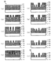
- FIG. 3 is a schematic process diagram showing an example of a method for manufacturing the phase shift mask 30 having the configuration shown in FIG.
- the transparent substrate 11 and the translucent layer 12 formed on the transparent substrate 11 are firstly shown.
- a hard mask layer 21 is formed on the light shielding layer 14 of the mask blank 10 having the intermediate layer 13 formed on the translucent layer and the light shielding layer 14 formed on the intermediate layer 13.
- a mask blank 20 with a hard mask layer is prepared.
- a first resist pattern film 51 is formed on the hard mask layer 21 by resist plate making using electron beam drawing or the like (FIG. 3B).
- the hard mask layer 21 exposed from the first resist pattern film 51 is etched by dry etching using a chlorine-based gas to form the hard mask pattern film 22 of the first form, and
- the light shielding layer 14 exposed from the hard mask pattern film 22 of the first form is etched by dry etching using a fluorine-based gas, and the intermediate layer 13 is used as an etching stop layer, so that the light shielding pattern film of the first form 64 is formed (FIG. 3C), and then the first resist pattern film 51 is removed (FIG. 3D).
- a second resist layer 52 is formed on the hard mask pattern film 22 of the first form and on the intermediate layer 13 exposed from the light shielding pattern film 64 of the first form (FIG. 3E ))
- the desired region of the hard mask pattern film 22 of the first form and the desired intermediate layer 13 exposed from the light shielding pattern film 64 of the first form are formed by resist plate making using electron beam drawing or the like.
- a second resist pattern film 53 is formed to cover this region (FIG. 3F).
- the hard mask pattern film 22 of the first form exposed from the second resist pattern film 53 and the second resist pattern film 53 and the first form are exposed by, for example, dry etching using a chlorine-based gas.
- the intermediate layer 13 exposed from the light shielding pattern film 64 is etched to form the second form of the hard mask pattern film 23 and the first form of the intermediate pattern film 63 (FIG. 3G).
- the second resist pattern film 53 is removed (FIG. 3H).
- the light shielding pattern film 64 exposed from the hard mask pattern film 23 of the second form and the half exposed from the intermediate pattern film 63 of the first form.
- the transparent layer 12 is etched to form the light shielding pattern film 34 and the semi-transparent pattern film 32 of the second form (FIG. 3 (i)).
- the hard mask pattern film 23 of the second form and the intermediate pattern film 63 of the first form exposed from the light shielding pattern film 34 of the second form are etched by, for example, dry etching using a chlorine-based gas. Then, while removing the hard mask pattern film 23 of the second form, the intermediate pattern film 33 of the second form is formed to obtain the phase shift mask 30 (FIG. 3J).
- FIG. 4 is a schematic process diagram showing an example of a method for manufacturing the phase shift mask 40 having the configuration shown in FIG.
- the transparent substrate 11 and the translucent layer 12 formed on the transparent substrate 11 are firstly obtained.
- a hard mask layer 21 is formed on the light shielding layer 14 of the mask blank 10 having the intermediate layer 13 formed on the translucent layer and the light shielding layer 14 formed on the intermediate layer 13.
- a mask blank 20 with a hard mask layer is prepared.
- a first resist pattern film 54 is formed on the hard mask layer 21 by resist plate making using electron beam drawing or the like (FIG. 4B).
- the hard mask layer 21 exposed from the first resist pattern film 54 is etched by dry etching using a chlorine-based gas to form the hard mask pattern film 24 of the first form, and then
- the light shielding layer 14 exposed from the hard mask pattern film 24 of the first form is etched by dry etching using a fluorine-based gas, and the intermediate layer 13 is used as an etching stop layer, so that the light shielding pattern film of the first form 74, and further, the intermediate layer 13 exposed from the light shielding pattern film 74 of the first form is etched to form the intermediate pattern film 73 of the first form (FIG. 4C).
- 1 resist pattern film 54 is removed (FIG. 4D).
- a second resist layer 55 is formed on the hard mask pattern film 24 of the first form and on the translucent layer 12 exposed from the intermediate pattern film 73 of the first form (FIG. 4 ( e))
- a second resist pattern film 56 covering a desired region of the hard mask pattern film 24 of the first form is formed by resist plate making using electron beam drawing or the like (FIG. 4F). .
- the hard mask pattern film 24 of the first form exposed from the second resist pattern film 56 is etched by, for example, dry etching using a chlorine-based gas, so that the hard mask pattern film 25 of the second form is etched. Is formed (FIG. 4G), and then the second resist pattern film 56 is removed (FIG. 4H).
- the light shielding pattern film 74 of the first form exposed from the hard mask pattern film 25 of the second form and the half exposed from the intermediate pattern film 73 of the first form.
- the transparent layer 12 is etched to form the light shielding pattern film 44 and the semi-transparent pattern film 42 of the second form (FIG. 4I).
- the hard mask pattern film 25 of the second form and the intermediate pattern film 73 of the first form exposed from the light shielding pattern film 44 of the second form are etched by, for example, dry etching using a chlorine-based gas. Then, while removing the hard mask pattern film 25 of the second form, the intermediate pattern film 43 of the second form is formed to obtain the phase shift mask 40 (FIG. 4J).
- Example 1-1 A 6-inch square, 0.25-inch thick synthetic quartz substrate optically polished is used as the transparent substrate 11, a molybdenum silicide oxide film (MoSiO) is used as the semitransparent layer 12, and a chromium film (Cr is 3 nm thick as the intermediate layer 13. ), A silicon film (Si) is used as the light shielding layer 14, and a chromium film (Cr) with a thickness of 3 nm is used as the hard mask layer 21, so that a mask blank 20 with a hard mask layer is prepared.
- MoSiO molybdenum silicide oxide film
- Cr chromium film
- Si silicon film
- Cr chromium film with a thickness of 3 nm
- the film thickness of the semi-transparent layer 12 is adjusted so that the transmittance with respect to the exposure light is 6%
- the film thickness of the light shielding layer 14 is three kinds of the semi-transparent layer 12, the intermediate layer 13, and the light shielding layer 14.
- the laminated body in which the above layers are laminated is adjusted so that the optical density with respect to the exposure light becomes 3.0.
- the above optical density can be measured with MCPD3000 manufactured by Otsuka Electronics Co., Ltd., and the optical constant can be obtained by measurement with an ellipsometer (manufactured by JA Woollam). Further, the film thickness can be obtained by step measurement using an AFM apparatus (SII Nano Technology).
- an electron beam resist is applied on the hard mask layer 21, and pattern drawing and development are performed by an electron beam drawing apparatus to form a first resist pattern film 51.
- the hard mask layer 21 is dry-etched with a mixed gas of chlorine and oxygen to form the hard mask pattern film 22 of the first embodiment.
- the light shielding layer 14 exposed from the hard mask pattern film 22 of the first form is etched by dry etching using CF 4 gas to form the light shielding pattern film 64 of the first form, and then The first resist pattern film 51 is removed by ashing with oxygen plasma.
- an electron beam resist as the second resist layer 52 is applied on the hard mask pattern film 22 of the first form and the intermediate layer 13 exposed from the light shielding pattern film 64 of the first form. Then, pattern drawing and development are performed by an electron beam drawing apparatus, and a second resist pattern film 53 is formed.
- the first form of the hard mask pattern film 22 exposed from the second resist pattern film 53 and the second resist pattern film 53 and the first resist are dry-etched using a mixed gas of chlorine and oxygen.
- the intermediate layer 13 exposed from the light shielding pattern film 64 of the form is etched to form the hard mask pattern film 23 of the second form and the intermediate pattern film 63 of the first form, and then the second resist pattern film 53 is removed by ashing with oxygen plasma.
- the light shielding pattern film 64 exposed from the hard mask pattern film 23 of the second form and the half exposed from the intermediate pattern film 63 of the first form.
- the transparent layer 12 is etched to form the light shielding pattern film 34 and the semi-transparent pattern film 32 of the second form.
- the hard mask pattern film 23 of the second form and the intermediate pattern film 63 of the first form exposed from the light shielding pattern film 34 of the second form are formed.
- the phase shift mask 30 of Example 1-1 is obtained by etching to form the intermediate pattern film 33 of the second form while removing the hard mask pattern film 23 of the second form.
- the etching rate with a fluorine-based gas is faster than that of a molybdenum silicide (MoSi) -based film, and the pattern processability is improved. Further, since the light shielding layer of the phase shift mask 30 is a silicon film, it exhibits higher chemical resistance and light resistance than a molybdenum silicide (MoSi) film.
- Example 1-2 The film thickness of the semi-transparent layer 12 is adjusted so that the transmittance with respect to the exposure light is 20%, and the three-layered structure of the semi-transparent layer 12, the intermediate layer 13, and the light shielding layer 14 is laminated with respect to the exposure light.
- a phase shift mask 30 of Example 1-2 is obtained in the same manner as in Example 1-1 except that the film thickness of the light shielding layer 14 is adjusted so that the optical density becomes 3.0.
- Example 1-3 The film thickness of the semi-transparent layer 12 is adjusted so that the transmittance with respect to the exposure light is 30%, and the three-layered structure of the semi-transparent layer 12, the intermediate layer 13, and the light shielding layer 14 is laminated with respect to the exposure light.
- a phase shift mask 30 of Example 1-3 is obtained in the same manner as in Example 1-1 except that the film thickness of the light shielding layer 14 is adjusted so that the optical density becomes 3.0.
- a molybdenum silicide nitride film (MoSiN) is formed to a thickness of 50 nm on an optically polished 6-inch square, 0.25-inch thick transparent synthetic quartz substrate, and a chromium film (Cr) is formed thereon.
- MoSiN molybdenum silicide nitride film
- Cr chromium film
- Binary photomask blanks having a structure of forming a hard mask layer by forming a film with a thickness of 3 nm are prepared.
- an electron beam resist is applied on the hard mask layer of the above blanks, and pattern drawing and development are performed by an electron beam drawing apparatus to form a resist pattern film having a desired shape.
- the hard mask layer chromium film is etched with a mixed gas of chlorine and oxygen, and the molybdenum silicide nitride film of the light shielding layer is dry etched using SF 6 gas. Then, a desired mask pattern is formed, and then the resist pattern film is removed by ashing with oxygen plasma. Next, the chromium film pattern of the hard mask layer is removed by etching with a mixed gas of chlorine and oxygen to obtain a binary photomask of Comparative Example 1-1.
- the thickness of the light shielding layer 14 can be changed within a range satisfying the above optical density. That is, when the translucency of the translucent layer 12 is small, the film thickness of the light shielding layer 14 can be reduced accordingly.
- the film thickness of the intermediate layer 13 is as extremely thin as 3 nm, and the material is also chromium-based, its light shielding property can be ignored.
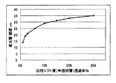
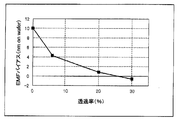
- the transmittance of the semitransparent layer 12 and the film thickness of the light shielding layer 14 satisfying the optical density of 3.0 between the two layers of the semitransparent layer 12 and the light shielding layer 14. The relationship is as shown in FIG.
- the thickness of the light shielding layer 14 satisfying the above condition is 25 nm.
- the transmittance of the semitransparent layer 12 is 20%
- the light shielding layer The film thickness of 14 is 33 nm.
- the transmissivity of the semitransparent layer 12 is 30%
- the film thickness of the light shielding layer 14 is 35 nm.
- middle layer 13, and the light shielding layer 14, is 2.8 or more.
- the light shielding layer 14 is preferably as thin as possible.
- Simulation conditions The simulation was performed under the following conditions.
- EM-Suite Version v6.00 (trade name: manufactured by Panoramic Technology) was used, and as a three-dimensional (also referred to as 3D) simulation condition, the simulation mode includes TEMPEST (EM -The FDTD method (also referred to as a time domain difference method or a finite difference time domain method) by Suite option) was used, and the grid size was set to 1 nm (in a quadruple mask).
- TEMPEST EM -The FDTD method (also referred to as a time domain difference method or a finite difference time domain method) by Suite option) was used, and the grid size was set to 1 nm (in a quadruple mask).
- 2D two-dimensional simulation condition
- the Kirchhoff method was used for the simulation mode.
- the exposure light source was an ArF excimer laser
- the exposure wavelength was 193 nm
- the numerical aperture (NA) of the projection lens was 1.35.
- the illumination system was exposure with oblique incident light using a pupil filter, and quadrupole illumination using a quadrupole (C-quad) pupil filter shown in FIG. 6 was set.
- the four light transmitting portions 91 of the C-quad form a fan shape with an opening angle of 20 degrees from the center of the pupil on the XY axis, and the mask pattern can be transferred with high resolution in the vertical and horizontal directions.
- the light transmitting portion 91 has an arrangement of 0 degrees and 90 degrees (XY polarization) and the radius of the pupil filter is 1, the outer diameter (outer ⁇ ) of the distance from the pupil center is 0.98, The inner diameter (inner ⁇ ) was 0.8.
- the portions other than the four light transmission portions 91 are light shielding portions 92 (shaded portions).
- the numerical aperture (NA) of 1.35 of the projection lens is used as an example because it is used for mask pattern transfer for fine semiconductor devices, and the present invention is originally limited thereto. However, it is possible to use lenses with other numerical apertures.
- the reason why quadrupole illumination is used as the illumination system is that quadrupole illumination can resolve vertical and horizontal patterns at the same time, has high universality, and can be applied to general mask pattern transfer. .
- the quadrupole illumination is used as a preferable example, and in the present invention, exposure variations are similarly applied to other modified illumination systems other than the quadrupole illumination, such as annular illumination and dipole illumination. The effect of improving the degree can be obtained.
- the EMF bias when forming an isolated hole pattern with a diameter of 40 nm on the resist on the wafer The evaluation result will be described with reference to FIG.
- the point where the transmittance is 0% indicates the value of the EMF bias of Comparative Example 1-1
- the point where the transmittance is 6% indicates the value of the EMF bias of Example 1-1
- the transmittance is 20%.
- the point represents the EMF bias value of Example 1-2
- the point of 30% transmittance represents the EMF bias value of Example 1-3.
- the value of the EMF bias in FIG. 7 indicates the size on the wafer. As shown in FIG.
- the conventional binary photomask of Comparative Example 1-1 requires an EMF bias of 10 nm in size on the wafer.
- the value of the EMF bias can be reduced.
- the value can be reduced to ⁇ 0.6 nm. The value of the EMF bias can be reduced.
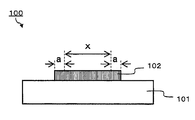
- FIG. 8 shows a binary mask 100 having a mask pattern made of a light shielding pattern film 102 on a transparent substrate 101.
- line CD Cross Dimension
- target CD target line width dimension
- the line CD is widened, and when the value of d is-, the line CD is narrowed.
- + in the case of +, in particular, + is not displayed.
- the EMF bias related to the electromagnetic field (EMF) effect greatly affects the critical dimension (CD) accuracy of the transfer pattern line width to the resist on the wafer. For this reason, it is necessary to correct the photomask pattern in order to simulate the electromagnetic field effect and suppress the influence of the electromagnetic field (EMF) effect when manufacturing the photomask.
- This mask pattern correction calculation becomes more complicated as the EMF bias increases. Also, the corrected mask pattern becomes more complex as the EMF bias is larger, and a larger load is applied to the photomask fabrication. For example, there is a problem that the bias value becomes large and the pattern cannot be corrected due to the relationship with the adjacent pattern. As the value of the EMF bias is closer to 0, the correction becomes smaller and the photomask manufacturing becomes easier, and the mask manufacturing yield is improved.
- the exposure margin (EL:%) is a range of exposure energy that allows the dimension of the resist pattern film on the wafer to be within an allowable limit, and a variation in exposure amount (dose amount) in photolithography. It is a value indicating the tolerance for. That is, the exposure energy range is such that the fluctuation amount of the line width dimension of the resist pattern falls within a predetermined allowable range. If the exposure margin is large, the yield in the photolithography process of manufacturing the semiconductor element is improved.
- the exposure margin (EL) at which the target CD at each pattern pitch (nm) on the wafer falls within ⁇ 10% is shown as the phase shift mask of Examples 1-1 to 1-3 and Comparative Example 1 -1 conventional binary photomasks were compared and evaluated.
- the evaluated mask pattern was a line and space pattern, and the through pitch (full pitch) when transferred onto the wafer was in the range of 80 nm to 300 nm, and the target line CD was 10 nm on the wafer.
- the phase shift masks according to the present invention of Examples 1-1 to 1-3 have the conventional binary photo of Comparative Example 1-1 in any range of pattern pitches of 80 nm to 300 nm. Compared with the mask, the exposure margin can be increased. In particular, in the phase shift mask of Example 1-3, the exposure margin is 1.8% at the pattern pitch of 80 nm, and the exposure margin of 1. A large value of 2% and an exposure margin of 0.8% at a pattern pitch of 300 nm was obtained.
- Example 2-1 A 6-inch square, 0.25-inch thick synthetic quartz substrate optically polished is used as the transparent substrate 11, a molybdenum silicide oxide film (MoSiO) is used as the semitransparent layer 12, and a CrN film with a thickness of 2 nm is used as the intermediate layer 13. Then, a mask blank 20 is produced using a silicon film (Si) as the light shielding layer 14.
- MoSiO molybdenum silicide oxide film
- CrN film with a thickness of 2 nm is used as the intermediate layer 13
- a mask blank 20 is produced using a silicon film (Si) as the light shielding layer 14.
- the film thickness of the semi-transparent layer 12 is adjusted so that the transmittance with respect to the exposure light is 6%
- the film thickness of the light shielding layer 14 is three kinds of the semi-transparent layer 12, the intermediate layer 13, and the light shielding layer 14.
- the laminated body in which the above layers are laminated is adjusted so that the optical density with respect to the exposure light becomes 3.0.
- the above optical density is measured with MCPD3000 manufactured by Otsuka Electronics Co., Ltd., and the optical constant is obtained by measurement with an ellipsometer (manufactured by JA Woollam).
- the film thickness is obtained by step measurement using an AFM apparatus (SII Nano Technology).
- Example 2-2 Except for using a CrN film with a thickness of 4 nm as the intermediate layer 13, a mask blank 20 is prepared in the same manner as in Example 2-1, and the film thickness of the semitransparent layer 12 and the film thickness of the light shielding layer 14 are adjusted. .
- a mask blank 20 is prepared in the same manner as in Example 2-1, and the thickness of the semitransparent layer 12 and the thickness of the light shielding layer 14 are adjusted. .
- the refractive index n and extinction coefficient k of the CrN film used for the intermediate layer 13 are 1.5 and 1.8, respectively, and the refractive index n and extinction of the silicon film (Si) used for the light shielding layer 14 are respectively.
- the coefficient k is 0.9 and 2.7, respectively.
- the film thickness of the intermediate layer 13 is 5 nm or more, the total film thickness of the intermediate layer 13 and the light shielding layer 14 is thicker than when the film thickness of the intermediate layer 13 is 5 nm or less. I understood it. For this reason, it is suggested that when the film thickness of the intermediate layer 13 is 5 nm or less, it is possible to avoid an increase in the value of the EMF bias of the phase shift mask.
- Example 3-1 Except for using a 2 nm-thickness CrON film as the intermediate layer 13, a mask blank 20 is prepared in the same manner as in Example 2-1, and the thickness of the semitransparent layer 12 and the thickness of the light shielding layer 14 are adjusted. .
- Example 3-2 Except for using a 4 nm-thickness CrON film as the intermediate layer 13, a mask blank 20 is produced in the same manner as in Example 2-1, and the film thickness of the semitransparent layer 12 and the film thickness of the light shielding layer 14 are adjusted. .
- the refractive index n and extinction coefficient k of the CrON film used for the intermediate layer 13 are 2.4 and 1.4, respectively, and the refractive index n and extinction of the silicon film (Si) used for the light shielding layer 14.
- the coefficient k is 0.9 and 2.7, respectively.
- the film thickness of the intermediate layer 13 is 5 nm or more, the total film thickness of the intermediate layer 13 and the light shielding layer 14 is thicker than when the film thickness of the intermediate layer 13 is 5 nm or less. I understood it. For this reason, it is suggested that when the film thickness of the intermediate layer 13 is 5 nm or less, it is possible to avoid an increase in the value of the EMF bias of the phase shift mask.
Landscapes
- Physics & Mathematics (AREA)
- General Physics & Mathematics (AREA)
- Preparing Plates And Mask In Photomechanical Process (AREA)
Priority Applications (4)
| Application Number | Priority Date | Filing Date | Title |
|---|---|---|---|
| KR1020167026750A KR102260188B1 (ko) | 2014-04-08 | 2015-01-29 | 마스크 블랭크, 위상 시프트 마스크 및 그 제조 방법 |
| DE112015001717.8T DE112015001717B4 (de) | 2013-08-20 | 2015-01-29 | Maskenrohling, Phasenverschiebungsmaske und Verfahren zur Herstellung derselben |
| US15/301,900 US9971238B2 (en) | 2013-08-20 | 2015-01-29 | Mask blank, phase shift mask, and production method thereof |
| CN201580015667.1A CN106133599B (zh) | 2013-08-20 | 2015-01-29 | 掩模坯料、相位位移掩模及其制造方法 |
Applications Claiming Priority (3)
| Application Number | Priority Date | Filing Date | Title |
|---|---|---|---|
| JP2013170739 | 2013-08-20 | ||
| JP2014079690A JP5686216B1 (ja) | 2013-08-20 | 2014-04-08 | マスクブランクス、位相シフトマスク及びその製造方法 |
| JP2014-079690 | 2014-04-08 |
Publications (1)
| Publication Number | Publication Date |
|---|---|
| WO2015156016A1 true WO2015156016A1 (ja) | 2015-10-15 |
Family
ID=52821412
Family Applications (1)
| Application Number | Title | Priority Date | Filing Date |
|---|---|---|---|
| PCT/JP2015/052495 WO2015156016A1 (ja) | 2013-08-20 | 2015-01-29 | マスクブランクス、位相シフトマスク及びその製造方法 |
Country Status (6)
Cited By (4)
| Publication number | Priority date | Publication date | Assignee | Title |
|---|---|---|---|---|
| CN108351604A (zh) * | 2016-01-27 | 2018-07-31 | 株式会社Lg化学 | 膜掩模、其制备方法、使用膜掩模的图案形成方法和由膜掩模形成的图案 |
| TWI659262B (zh) * | 2017-08-07 | 2019-05-11 | 日商Hoya股份有限公司 | 光罩之修正方法、光罩之製造方法、光罩及顯示裝置之製造方法 |
| WO2020012733A1 (ja) * | 2018-07-09 | 2020-01-16 | 株式会社村田製作所 | 人工水晶部材及びそれを用いた光学素子 |
| TWI832788B (zh) * | 2016-03-02 | 2024-02-11 | 日商信越化學工業股份有限公司 | 光罩空白基板及光罩之製造方法 |
Families Citing this family (21)
| Publication number | Priority date | Publication date | Assignee | Title |
|---|---|---|---|---|
| US9341940B2 (en) * | 2014-05-15 | 2016-05-17 | Taiwan Semiconductor Manufacturing Co., Ltd. | Reticle and method of fabricating the same |
| JP6511860B2 (ja) * | 2015-02-27 | 2019-05-15 | 富士通株式会社 | 表示制御システム、グラフ表示方法およびグラフ表示プログラム |
| JP6341129B2 (ja) * | 2015-03-31 | 2018-06-13 | 信越化学工業株式会社 | ハーフトーン位相シフトマスクブランク及びハーフトーン位相シフトマスク |
| US9921467B2 (en) * | 2015-11-30 | 2018-03-20 | Taiwan Semiconductor Manufacturing Company Ltd. | Mask blank and mask and fabrication method thereof |
| CN108073032B (zh) * | 2016-11-18 | 2021-06-08 | 台湾积体电路制造股份有限公司 | 相位移光掩模的形成方法 |
| JP6642493B2 (ja) * | 2017-03-10 | 2020-02-05 | 信越化学工業株式会社 | ハーフトーン位相シフト型フォトマスクブランク |
| JP6791031B2 (ja) * | 2017-06-13 | 2020-11-25 | 信越化学工業株式会社 | フォトマスクブランク及びその製造方法 |
| CN110770652B (zh) * | 2017-06-14 | 2023-03-21 | Hoya株式会社 | 掩模坯料、相移掩模及半导体器件的制造方法 |
| US11086211B2 (en) * | 2017-11-08 | 2021-08-10 | Taiwan Semiconductor Manufacturing Company, Ltd. | Masks and methods of forming the same |
| KR102504179B1 (ko) * | 2017-12-21 | 2023-02-28 | 에스케이하이닉스 주식회사 | 쉐이딩층을 내장한 포토 마스크 및 이를 이용한 패턴 형성 방법 |
| KR20200133377A (ko) * | 2018-03-26 | 2020-11-27 | 호야 가부시키가이샤 | 마스크 블랭크, 위상 시프트 마스크 및 반도체 디바이스의 제조 방법 |
| JP7214593B2 (ja) | 2019-08-13 | 2023-01-30 | キオクシア株式会社 | フォトマスクの製造方法 |
| TWI707195B (zh) * | 2020-02-14 | 2020-10-11 | 力晶積成電子製造股份有限公司 | 相位轉移光罩的製造方法 |
| CN112563440A (zh) * | 2020-12-01 | 2021-03-26 | 京东方科技集团股份有限公司 | 掩膜板及其制备方法、显示面板的制备方法 |
| JP7570255B2 (ja) * | 2021-03-04 | 2024-10-21 | 株式会社エスケーエレクトロニクス | 多階調フォトマスクの製造方法及び多階調フォトマスク |
| KR102465982B1 (ko) * | 2021-07-13 | 2022-11-09 | 에스케이씨솔믹스 주식회사 | 블랭크 마스크 및 이를 이용한 포토마스크 |
| CN113608407B (zh) * | 2021-08-18 | 2023-12-05 | 业成科技(成都)有限公司 | 掩膜、其制备方法及曝光方法 |
| CN114415268B (zh) * | 2022-01-28 | 2024-07-12 | 宁波舜宇奥来技术有限公司 | 光学相位板的制作方法 |
| JP2024006265A (ja) * | 2022-07-01 | 2024-01-17 | 株式会社エスケーエレクトロニクス | フォトマスクの製造方法及びフォトマスク |
| CN115586697B (zh) * | 2022-08-31 | 2025-04-11 | 睿晶半导体(宁波)有限公司 | 光掩膜版及其制作方法 |
| JP7450784B1 (ja) * | 2023-04-10 | 2024-03-15 | 株式会社エスケーエレクトロニクス | フォトマスクの製造方法 |
Citations (3)
| Publication number | Priority date | Publication date | Assignee | Title |
|---|---|---|---|---|
| JPH1126355A (ja) * | 1997-07-07 | 1999-01-29 | Toshiba Corp | 露光用マスク及びその製造方法 |
| JP2002251000A (ja) * | 2001-02-26 | 2002-09-06 | Semiconductor Leading Edge Technologies Inc | 位相シフトマスクの製造方法、位相シフトマスク、位相シフトマスクブランクス及び半導体装置の製造方法 |
| JP2012003287A (ja) * | 2011-09-21 | 2012-01-05 | Shin Etsu Chem Co Ltd | フォトマスクの製造方法及びフォトマスク |
Family Cites Families (18)
| Publication number | Priority date | Publication date | Assignee | Title |
|---|---|---|---|---|
| JPH07199447A (ja) * | 1993-12-28 | 1995-08-04 | Sony Corp | 単層ハーフトーン方式位相シフトマスク及びその作製方法 |
| JP3209257B2 (ja) | 1995-04-21 | 2001-09-17 | 凸版印刷株式会社 | 位相シフトマスク及びその製造方法 |
| US6855463B2 (en) * | 2002-08-27 | 2005-02-15 | Photronics, Inc. | Photomask having an intermediate inspection film layer |
| US7862960B2 (en) * | 2004-06-22 | 2011-01-04 | Hoya Corporation | Manufacturing method of transparent substrate for mask blanks, manufacturing method of mask blanks, manufacturing method of exposure masks, manufacturing method of semiconductor devices, manufacturing method of liquid crystal display devices, and defect correction method of exposure masks |
| TW200639576A (en) * | 2005-02-28 | 2006-11-16 | Hoya Corp | Method of manufacturing gray level mask, gray level mask, and gray level mask blank |
| CN102520577B (zh) * | 2005-08-11 | 2014-10-29 | 富士通半导体股份有限公司 | 曝光用掩模、图案复制方法 |
| EP1804119A1 (en) * | 2005-12-27 | 2007-07-04 | Interuniversitair Microelektronica Centrum | Method for manufacturing attenuated phase- shift masks and devices obtained therefrom |
| JP4883278B2 (ja) | 2006-03-10 | 2012-02-22 | 信越化学工業株式会社 | フォトマスクブランク及びフォトマスクの製造方法 |
| JP4764214B2 (ja) * | 2006-03-10 | 2011-08-31 | 凸版印刷株式会社 | ハーフトーン型位相シフトマスク及びその製造方法 |
| JP4737426B2 (ja) * | 2006-04-21 | 2011-08-03 | 信越化学工業株式会社 | フォトマスクブランク |
| JP4853684B2 (ja) * | 2009-03-31 | 2012-01-11 | 信越化学工業株式会社 | フォトマスクブランク及びフォトマスク |
| KR101656456B1 (ko) * | 2009-10-30 | 2016-09-12 | 삼성전자주식회사 | 하프톤형 위상반전 블랭크 포토마스크와 하프톤형 위상반전 포토마스크 및 그의 제조방법 |
| JP2011215197A (ja) * | 2010-03-31 | 2011-10-27 | Hoya Corp | フォトマスク及びその製造方法 |
| JP5400698B2 (ja) | 2010-04-28 | 2014-01-29 | Hoya株式会社 | 多階調フォトマスク、多階調フォトマスクの製造方法、パターン転写方法及び多階調フォトマスクの使用方法 |
| JP5682493B2 (ja) * | 2010-08-04 | 2015-03-11 | 信越化学工業株式会社 | バイナリーフォトマスクブランク及びバイナリーフォトマスクの製造方法 |
| JP5464186B2 (ja) * | 2011-09-07 | 2014-04-09 | 信越化学工業株式会社 | フォトマスクブランク、フォトマスク及びその製造方法 |
| JP2014191176A (ja) * | 2013-03-27 | 2014-10-06 | Dainippon Printing Co Ltd | フォトマスクブランクス、フォトマスク及びその製造方法 |
| JP2015194673A (ja) | 2013-08-21 | 2015-11-05 | 大日本印刷株式会社 | マスクブランクス、ネガ型レジスト膜付きマスクブランクス、位相シフトマスク、およびそれを用いるパターン形成体の製造方法 |
-
2014
- 2014-04-08 JP JP2014079690A patent/JP5686216B1/ja active Active
-
2015
- 2015-01-20 JP JP2015008587A patent/JP6394410B2/ja active Active
- 2015-01-29 DE DE112015001717.8T patent/DE112015001717B4/de active Active
- 2015-01-29 US US15/301,900 patent/US9971238B2/en active Active
- 2015-01-29 WO PCT/JP2015/052495 patent/WO2015156016A1/ja active Application Filing
- 2015-01-29 CN CN201580015667.1A patent/CN106133599B/zh active Active
- 2015-01-30 TW TW104103190A patent/TWI575305B/zh active
Patent Citations (3)
| Publication number | Priority date | Publication date | Assignee | Title |
|---|---|---|---|---|
| JPH1126355A (ja) * | 1997-07-07 | 1999-01-29 | Toshiba Corp | 露光用マスク及びその製造方法 |
| JP2002251000A (ja) * | 2001-02-26 | 2002-09-06 | Semiconductor Leading Edge Technologies Inc | 位相シフトマスクの製造方法、位相シフトマスク、位相シフトマスクブランクス及び半導体装置の製造方法 |
| JP2012003287A (ja) * | 2011-09-21 | 2012-01-05 | Shin Etsu Chem Co Ltd | フォトマスクの製造方法及びフォトマスク |
Cited By (5)
| Publication number | Priority date | Publication date | Assignee | Title |
|---|---|---|---|---|
| CN108351604A (zh) * | 2016-01-27 | 2018-07-31 | 株式会社Lg化学 | 膜掩模、其制备方法、使用膜掩模的图案形成方法和由膜掩模形成的图案 |
| CN108351604B (zh) * | 2016-01-27 | 2020-10-30 | 株式会社Lg化学 | 膜掩模、其制备方法、使用膜掩模的图案形成方法和由膜掩模形成的图案 |
| TWI832788B (zh) * | 2016-03-02 | 2024-02-11 | 日商信越化學工業股份有限公司 | 光罩空白基板及光罩之製造方法 |
| TWI659262B (zh) * | 2017-08-07 | 2019-05-11 | 日商Hoya股份有限公司 | 光罩之修正方法、光罩之製造方法、光罩及顯示裝置之製造方法 |
| WO2020012733A1 (ja) * | 2018-07-09 | 2020-01-16 | 株式会社村田製作所 | 人工水晶部材及びそれを用いた光学素子 |
Also Published As
| Publication number | Publication date |
|---|---|
| DE112015001717T5 (de) | 2016-12-29 |
| JP5686216B1 (ja) | 2015-03-18 |
| US9971238B2 (en) | 2018-05-15 |
| JP2015062049A (ja) | 2015-04-02 |
| TW201539112A (zh) | 2015-10-16 |
| TWI575305B (zh) | 2017-03-21 |
| CN106133599B (zh) | 2019-09-03 |
| US20170123305A1 (en) | 2017-05-04 |
| JP6394410B2 (ja) | 2018-09-26 |
| CN106133599A (zh) | 2016-11-16 |
| DE112015001717B4 (de) | 2024-06-13 |
| JP2015092281A (ja) | 2015-05-14 |
Similar Documents
| Publication | Publication Date | Title |
|---|---|---|
| JP6394410B2 (ja) | マスクブランクス、位相シフトマスク及びその製造方法 | |
| KR101935171B1 (ko) | 표시 장치 제조용의 위상 시프트 마스크 블랭크, 표시 장치 제조용의 위상 시프트 마스크 및 그 제조 방법, 및 표시 장치의 제조 방법 | |
| JP5524828B2 (ja) | 反射型マスクブランク、反射型マスク及びその製造方法 | |
| TWI684059B (zh) | 半色調相位移光罩基板及半色調相位移光罩 | |
| WO2015025922A1 (ja) | マスクブランクス、ネガ型レジスト膜付きマスクブランクス、位相シフトマスク、およびそれを用いるパターン形成体の製造方法 | |
| KR101899202B1 (ko) | 하프톤 위상 시프트 마스크 블랭크, 하프톤 위상 시프트 마스크 및 패턴 노광 방법 | |
| KR101923272B1 (ko) | 포토마스크 블랭크, 그의 제조 방법 및 포토마스크 | |
| JP6524614B2 (ja) | マスクブランクス、ネガ型レジスト膜付きマスクブランクス、位相シフトマスク、およびそれを用いるパターン形成体の製造方法 | |
| KR20160010322A (ko) | 포토마스크, 포토마스크의 제조 방법, 포토마스크 블랭크 및 표시 장치의 제조 방법 | |
| TWI659262B (zh) | 光罩之修正方法、光罩之製造方法、光罩及顯示裝置之製造方法 | |
| KR20190010686A (ko) | 마스크 블랭크, 전사용 마스크, 전사용 마스크의 제조 방법 및 반도체 디바이스의 제조 방법 | |
| JP2014191176A (ja) | フォトマスクブランクス、フォトマスク及びその製造方法 | |
| KR102260188B1 (ko) | 마스크 블랭크, 위상 시프트 마스크 및 그 제조 방법 | |
| JP4997902B2 (ja) | ハーフトーンマスク | |
| JP6315033B2 (ja) | フォトマスク | |
| JP2015062050A (ja) | マスクブランクス、ネガ型レジスト膜付きマスクブランクス、位相シフトマスク、およびそれを用いるパターン形成体の製造方法 | |
| JP5239799B2 (ja) | ハーフトーン型位相シフトマスク | |
| JP6035884B2 (ja) | フォトマスクの製造方法 |
Legal Events
| Date | Code | Title | Description |
|---|---|---|---|
| 121 | Ep: the epo has been informed by wipo that ep was designated in this application |
Ref document number: 15776115 Country of ref document: EP Kind code of ref document: A1 |
|
| ENP | Entry into the national phase |
Ref document number: 20167026750 Country of ref document: KR Kind code of ref document: A |
|
| WWE | Wipo information: entry into national phase |
Ref document number: 15301900 Country of ref document: US |
|
| WWE | Wipo information: entry into national phase |
Ref document number: 112015001717 Country of ref document: DE |
|
| 122 | Ep: pct application non-entry in european phase |
Ref document number: 15776115 Country of ref document: EP Kind code of ref document: A1 |