WO2015151786A1 - 可変容量デバイスおよびその製造方法 - Google Patents
可変容量デバイスおよびその製造方法 Download PDFInfo
- Publication number
- WO2015151786A1 WO2015151786A1 PCT/JP2015/057814 JP2015057814W WO2015151786A1 WO 2015151786 A1 WO2015151786 A1 WO 2015151786A1 JP 2015057814 W JP2015057814 W JP 2015057814W WO 2015151786 A1 WO2015151786 A1 WO 2015151786A1
- Authority
- WO
- WIPO (PCT)
- Prior art keywords
- variable capacitance
- film
- input
- output terminal
- terminal
- Prior art date
Links
- 238000004519 manufacturing process Methods 0.000 title claims description 21
- 239000000758 substrate Substances 0.000 claims abstract description 41
- 239000004065 semiconductor Substances 0.000 claims abstract description 34
- 239000003990 capacitor Substances 0.000 claims abstract description 23
- 239000010409 thin film Substances 0.000 claims abstract description 16
- 239000010410 layer Substances 0.000 claims description 42
- 238000000034 method Methods 0.000 claims description 12
- 239000004020 conductor Substances 0.000 claims description 2
- 239000011229 interlayer Substances 0.000 claims description 2
- 239000010408 film Substances 0.000 description 106
- 229910004298 SiO 2 Inorganic materials 0.000 description 19
- 229920002577 polybenzoxazole Polymers 0.000 description 18
- 238000004891 communication Methods 0.000 description 11
- 229910000679 solder Inorganic materials 0.000 description 11
- 238000000059 patterning Methods 0.000 description 9
- 238000004544 sputter deposition Methods 0.000 description 9
- 238000002955 isolation Methods 0.000 description 7
- 238000010586 diagram Methods 0.000 description 6
- 230000008569 process Effects 0.000 description 5
- 230000035945 sensitivity Effects 0.000 description 5
- 230000005540 biological transmission Effects 0.000 description 4
- 238000009792 diffusion process Methods 0.000 description 4
- 230000002411 adverse Effects 0.000 description 3
- 230000015572 biosynthetic process Effects 0.000 description 3
- 230000008859 change Effects 0.000 description 3
- 239000012535 impurity Substances 0.000 description 3
- 238000005468 ion implantation Methods 0.000 description 3
- 239000011241 protective layer Substances 0.000 description 3
- 238000004528 spin coating Methods 0.000 description 3
- 239000011248 coating agent Substances 0.000 description 2
- 238000000576 coating method Methods 0.000 description 2
- 230000005684 electric field Effects 0.000 description 2
- 238000010438 heat treatment Methods 0.000 description 2
- 229910052751 metal Inorganic materials 0.000 description 2
- 239000002184 metal Substances 0.000 description 2
- 239000007769 metal material Substances 0.000 description 2
- 238000000206 photolithography Methods 0.000 description 2
- WFKWXMTUELFFGS-UHFFFAOYSA-N tungsten Chemical compound [W] WFKWXMTUELFFGS-UHFFFAOYSA-N 0.000 description 2
- 229910052721 tungsten Inorganic materials 0.000 description 2
- 239000010937 tungsten Substances 0.000 description 2
- 238000005229 chemical vapour deposition Methods 0.000 description 1
- VNNRSPGTAMTISX-UHFFFAOYSA-N chromium nickel Chemical compound [Cr].[Ni] VNNRSPGTAMTISX-UHFFFAOYSA-N 0.000 description 1
- 230000008878 coupling Effects 0.000 description 1
- 238000010168 coupling process Methods 0.000 description 1
- 238000005859 coupling reaction Methods 0.000 description 1
- 238000005520 cutting process Methods 0.000 description 1
- 230000000694 effects Effects 0.000 description 1
- 238000005530 etching Methods 0.000 description 1
- 238000010304 firing Methods 0.000 description 1
- 238000009616 inductively coupled plasma Methods 0.000 description 1
- 239000000463 material Substances 0.000 description 1
- 229910052750 molybdenum Inorganic materials 0.000 description 1
- 229910001120 nichrome Inorganic materials 0.000 description 1
- 229910000510 noble metal Inorganic materials 0.000 description 1
- 230000003647 oxidation Effects 0.000 description 1
- 238000007254 oxidation reaction Methods 0.000 description 1
- 238000001020 plasma etching Methods 0.000 description 1
- 238000007747 plating Methods 0.000 description 1
- 229910052697 platinum Inorganic materials 0.000 description 1
- 230000010287 polarization Effects 0.000 description 1
- 230000001681 protective effect Effects 0.000 description 1
- 230000009467 reduction Effects 0.000 description 1
- 238000005549 size reduction Methods 0.000 description 1
- WQJQOUPTWCFRMM-UHFFFAOYSA-N tungsten disilicide Chemical compound [Si]#[W]#[Si] WQJQOUPTWCFRMM-UHFFFAOYSA-N 0.000 description 1
- 229910021342 tungsten silicide Inorganic materials 0.000 description 1
Images


Classifications
-
- H—ELECTRICITY
- H01—ELECTRIC ELEMENTS
- H01L—SEMICONDUCTOR DEVICES NOT COVERED BY CLASS H10
- H01L27/00—Devices consisting of a plurality of semiconductor or other solid-state components formed in or on a common substrate
- H01L27/02—Devices consisting of a plurality of semiconductor or other solid-state components formed in or on a common substrate including semiconductor components specially adapted for rectifying, oscillating, amplifying or switching and having at least one potential-jump barrier or surface barrier; including integrated passive circuit elements with at least one potential-jump barrier or surface barrier
- H01L27/0203—Particular design considerations for integrated circuits
- H01L27/0248—Particular design considerations for integrated circuits for electrical or thermal protection, e.g. electrostatic discharge [ESD] protection
-
- B—PERFORMING OPERATIONS; TRANSPORTING
- B81—MICROSTRUCTURAL TECHNOLOGY
- B81B—MICROSTRUCTURAL DEVICES OR SYSTEMS, e.g. MICROMECHANICAL DEVICES
- B81B7/00—Microstructural systems; Auxiliary parts of microstructural devices or systems
- B81B7/0009—Structural features, others than packages, for protecting a device against environmental influences
- B81B7/0022—Protection against electrostatic discharge
-
- H—ELECTRICITY
- H01—ELECTRIC ELEMENTS
- H01G—CAPACITORS; CAPACITORS, RECTIFIERS, DETECTORS, SWITCHING DEVICES OR LIGHT-SENSITIVE DEVICES, OF THE ELECTROLYTIC TYPE
- H01G7/00—Capacitors in which the capacitance is varied by non-mechanical means; Processes of their manufacture
- H01G7/06—Capacitors in which the capacitance is varied by non-mechanical means; Processes of their manufacture having a dielectric selected for the variation of its permittivity with applied voltage, i.e. ferroelectric capacitors
-
- H—ELECTRICITY
- H01—ELECTRIC ELEMENTS
- H01L—SEMICONDUCTOR DEVICES NOT COVERED BY CLASS H10
- H01L27/00—Devices consisting of a plurality of semiconductor or other solid-state components formed in or on a common substrate
- H01L27/02—Devices consisting of a plurality of semiconductor or other solid-state components formed in or on a common substrate including semiconductor components specially adapted for rectifying, oscillating, amplifying or switching and having at least one potential-jump barrier or surface barrier; including integrated passive circuit elements with at least one potential-jump barrier or surface barrier
- H01L27/04—Devices consisting of a plurality of semiconductor or other solid-state components formed in or on a common substrate including semiconductor components specially adapted for rectifying, oscillating, amplifying or switching and having at least one potential-jump barrier or surface barrier; including integrated passive circuit elements with at least one potential-jump barrier or surface barrier the substrate being a semiconductor body
- H01L27/08—Devices consisting of a plurality of semiconductor or other solid-state components formed in or on a common substrate including semiconductor components specially adapted for rectifying, oscillating, amplifying or switching and having at least one potential-jump barrier or surface barrier; including integrated passive circuit elements with at least one potential-jump barrier or surface barrier the substrate being a semiconductor body including only semiconductor components of a single kind
- H01L27/0805—Capacitors only
-
- H—ELECTRICITY
- H01—ELECTRIC ELEMENTS
- H01L—SEMICONDUCTOR DEVICES NOT COVERED BY CLASS H10
- H01L29/00—Semiconductor devices adapted for rectifying, amplifying, oscillating or switching, or capacitors or resistors with at least one potential-jump barrier or surface barrier, e.g. PN junction depletion layer or carrier concentration layer; Details of semiconductor bodies or of electrodes thereof ; Multistep manufacturing processes therefor
- H01L29/66—Types of semiconductor device ; Multistep manufacturing processes therefor
- H01L29/86—Types of semiconductor device ; Multistep manufacturing processes therefor controllable only by variation of the electric current supplied, or only the electric potential applied, to one or more of the electrodes carrying the current to be rectified, amplified, oscillated or switched
- H01L29/92—Capacitors with potential-jump barrier or surface barrier
- H01L29/93—Variable capacitance diodes, e.g. varactors
-
- B—PERFORMING OPERATIONS; TRANSPORTING
- B81—MICROSTRUCTURAL TECHNOLOGY
- B81B—MICROSTRUCTURAL DEVICES OR SYSTEMS, e.g. MICROMECHANICAL DEVICES
- B81B2201/00—Specific applications of microelectromechanical systems
- B81B2201/02—Sensors
- B81B2201/0221—Variable capacitors
-
- H—ELECTRICITY
- H01—ELECTRIC ELEMENTS
- H01G—CAPACITORS; CAPACITORS, RECTIFIERS, DETECTORS, SWITCHING DEVICES OR LIGHT-SENSITIVE DEVICES, OF THE ELECTROLYTIC TYPE
- H01G4/00—Fixed capacitors; Processes of their manufacture
- H01G4/33—Thin- or thick-film capacitors
-
- H—ELECTRICITY
- H01—ELECTRIC ELEMENTS
- H01L—SEMICONDUCTOR DEVICES NOT COVERED BY CLASS H10
- H01L28/00—Passive two-terminal components without a potential-jump or surface barrier for integrated circuits; Details thereof; Multistep manufacturing processes therefor
- H01L28/40—Capacitors
- H01L28/55—Capacitors with a dielectric comprising a perovskite structure material
Definitions
- the present invention relates to a variable capacitance device used in a communication apparatus such as an RFID (Radio Frequency Identification) system and a near field communication (NFC) system, and a manufacturing method thereof.
- a communication apparatus such as an RFID (Radio Frequency Identification) system and a near field communication (NFC) system
- NFC near field communication
- variable capacitance elements whose permittivity changes by application of a control voltage have been proposed.
- These variable capacitance elements have a laminated structure (MIM structure) of metal, a ferroelectric material, and a metal, and are provided with a thin film ferroelectric so that a large capacitance change amount can be obtained at a low voltage.
- a variable capacitance element including a ferroelectric film has a low ESD (Electro-Static Discharge) characteristic compared to a semiconductor variable capacitance element such as a MEMS variable capacitance element or a variable capacitance diode. It was.
- the control sensitivity ratio of change in capacitance value with respect to the change in control voltage
- the ESD resistance is deteriorated as the ferroelectric film is made thinner. That is, when ESD exceeding ESD resistance occurs, the surge is applied to the ferroelectric film, and the ferroelectric film is dielectrically broken down. For this reason, from the viewpoint of ESD resistance, there is a restriction on the thinning of the ferroelectric film, and thus the control sensitivity is also restricted.
- An object of the present invention is to provide a variable capacitance device having high ESD resistance.
- the variable capacitance device of the present invention is A semiconductor substrate, a redistribution layer provided on the main surface thereof, and a plurality of terminal electrodes including a first input / output terminal, a second input / output terminal, and a ground terminal, A ferroelectric thin film comprising a pair of capacitor electrodes respectively connected to the first input / output terminal and the second input / output terminal and a ferroelectric thin film disposed between the pair of capacitor electrodes on the rewiring layer.
- Type variable capacitance element part is formed,
- An ESD protection element connected between the first input / output terminal or the second input / output terminal and the ground terminal is formed on the semiconductor substrate.
- variable capacitance element portion is formed on the rewiring layer, and the ESD protection element is formed on the semiconductor substrate.
- the variable capacitance element portion is formed on the rewiring layer, and the ESD protection element is formed on the semiconductor substrate.
- the main surface of the semiconductor substrate is provided with an electrode pad for connecting the ESD protection element to the ground terminal and the first input / output terminal or the second input / output terminal.
- the electrode pad is formed of W or WSi. It is preferable that As a result, the variable capacitance element portion having the ferroelectric thin film layer that has high heat resistance of the pad electrode of the semiconductor substrate and requires heat treatment at a high temperature can be incorporated into the rewiring layer.
- variable capacitance element portion is preferably provided at a position that does not overlap the ESD protection element and the electrode pad of the ESD protection element. As a result, it becomes easier to ensure the isolation between the variable capacitance element portion and the ESD protection element portion, and the flatness of the underlying portion of the variable capacitance element portion can be ensured, and the reliability of the variable capacitance element portion can be improved.
- a resistance element is provided between the variable capacitance element portion and the control voltage application terminal, and the resistance element is on the opposite side of the semiconductor substrate with respect to the layer in which the variable capacitance element portion is provided in the rewiring layer. It is preferable to be formed in a layer. Accordingly, it is not necessary to provide a resistance element outside, and the number of elements can be greatly reduced. In addition, since the resistance element is formed in a layer opposite to the semiconductor substrate with respect to the layer provided with the variable capacitance element portion, it does not adversely affect the flatness of the variable capacitance element portion, and the ESD protection element portion And the resistance element can be improved.
- an insulating layer is provided between the variable capacitance element portion and the semiconductor substrate. That is, by forming an insulating layer between the semiconductor substrate and the capacitor electrode, it is possible to further improve the isolation between the ESD protection part and the variable capacitance element part.
- the method for manufacturing the variable capacitance device of the present invention includes: Forming an ESD protection element on a semiconductor substrate; Forming a ferroelectric thin film type variable capacitance element portion comprising a pair of capacitor electrodes and a ferroelectric thin film disposed between the pair of capacitor electrodes on the main surface of the semiconductor substrate; Forming an insulating layer covering the variable capacitance element portion on the main surface of the semiconductor substrate; Forming an interlayer connection conductor and a terminal electrode connected to the ESD protection element and the variable capacitance element portion on the insulating layer.
- a small variable capacitance device can be obtained while having high control sensitivity and ESD resistance.
- FIG. 3 is a circuit diagram of a variable capacitance device 91 according to the first embodiment.
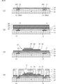
- FIG. 3 is a schematic sectional view of a variable capacitance device 91.
- FIG. 7 is a cross-sectional view showing a detailed structure and manufacturing method of a variable capacitance device 91.
- FIG. It is sectional drawing which shows the detailed structure and manufacturing method of the variable capacity device 91 following FIG. 3A.
- 6 is a plan view of the variable capacitance device 91 as viewed from the mounting surface side.
- FIG. 5B is a cross-sectional view illustrating the structure and manufacturing method of the variable capacitance device 92 following FIG. 5A.
- FIG. 3 is a schematic diagram showing an element arrangement inside a variable capacitance device 92.
- FIG. 6A is a schematic plan view
- FIG. 6B is a schematic front view.
- 7 is a cross-sectional view showing the structure and manufacturing method of a variable capacitance device 93.
- FIG. 8B is a cross-sectional view illustrating the structure and manufacturing method of the variable capacitance device 93, following FIG. 8B.
- 8C is a cross-sectional view illustrating the structure and manufacturing method of the variable capacitance device 93, following FIG. 8C.
- 8D is a cross-sectional view illustrating the structure and manufacturing method of the variable capacitance device 93, following FIG. 8D.
- FIG. 1 is a circuit diagram of a variable capacitance device 91 according to the first embodiment.
- the variable capacitance device 91 includes variable capacitance elements C1 to C6, RF resistance elements R11 to R19, and ESD protection elements ESDP1 and ESDP2.
- the capacitance values of the variable capacitance elements C1 to C6 are determined according to the control voltage applied between the control voltage input terminal Vt and the ground terminal GND, and thereby, between the first input / output terminal P1 and the second input / output terminal P2.
- the capacity value is determined.
- Each of the variable capacitance elements C1 to C6 is a ferroelectric capacitor composed of a ferroelectric film whose dielectric constant is changed by an electric field, and a capacitor electrode to which a voltage is applied across the ferroelectric film. Since the dielectric constant of the ferroelectric film is changed by changing the polarization amount according to the strength of the applied electric field, the capacitance value can be determined by the control voltage.
- a control voltage is applied to each capacitor electrode via RF resistance elements R11 to R19. The resistance values of the RF resistance elements R11 to R19 are equal.
- RF resistance elements R11 to R19 apply a control voltage to each of the variable capacitance elements C1 to C6, and an RF signal applied between the terminals P1 and P2 leaks to the control voltage input terminal Vt and the ground terminal GND. Acts as a choke resistor that suppresses
- An ESD protection element ESDP1 made of a Zener diode is connected between the first input / output terminal P1 and the ground terminal GND, and an ESD protection element ESDP2 is connected between the second input / output terminal P2 and the ground terminal GND.
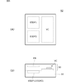
- FIG. 2 is a schematic cross-sectional view of the variable capacitance device 91.
- a substrate 10 is a Si substrate having a protective film formed on the surface.
- ESD protection elements ESDP1 and ESDP2 are formed on the surface of the Si substrate 10.
- the variable capacitance element portion VC and the resistance element portion RN are formed in the rewiring layer 50 on the Si substrate 10.
- a plurality of terminal electrodes PE are formed on the surface of the rewiring layer 50. These terminal electrodes PE are used as mounting terminals for mounting the variable capacitance device 91 on a printed wiring board.
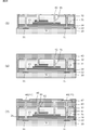
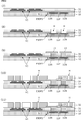
- FIG. 3A and 3B are cross-sectional views showing the detailed structure and manufacturing method of the variable capacitance device 91.
- FIG. Hereinafter, with reference to FIG. 3A and FIG.
- An SiO 2 film 12 is formed on the Si substrate 10, and an active region 11 by impurity diffusion is formed by ion implantation or the like in a region where an ESD protection element is to be formed. Subsequently, an electrode pad 13 made of W (tungsten) conducting to the active region 11 is formed, and a SiN insulating film 14 is formed on the entire surface by, eg, CVD.
- the SiO 2 film 12 and the SiN insulating film 14 are provided for the purpose of preventing mutual diffusion between the BST film 21 and the Si substrate 10 described below.
- BST film A (Ba, Sr) TiO 3 film (hereinafter referred to as “BST film”) 21, a Pt electrode film 22, a BST film 23, a Pt electrode film 24, and a BST film 25 are sequentially formed on the insulating film 14.
- BST films are formed by a spin coating process and a baking process, and the Pt film is formed by sputtering.
- the BST film 21 is used as an adhesion layer for the SiN insulating film 14. Since the BST film 21 is not related to the capacitance, it may be other than the BST film as long as it functions as an adhesion layer for the SiN insulating film 14.
- the Pt film can also be made of another high-melting-point noble metal material that has good conductivity and excellent oxidation resistance, such as Au.
- the baking temperature of the BST film is 600 ° C. to 700 ° C. With this heat, the portion of the electrode pad 13 in contact with the active region 11 becomes WSi (tungsten silicide).
- variable capacitor element VC is formed by patterning the Pt electrode films 22 and 24 and the BST films 23 and 25 by photolithography for a predetermined number of times.
- a SiO 2 film 31 is formed by CVD or sputtering, and a PBO (polybenzoxazole) film is applied thereon by an automatic coater and baked to form a PBO film 32 as an organic protective layer. . Then, an opening H is formed by inductively coupled plasma reactive ion etching (ICP-RIE).
- ICP-RIE inductively coupled plasma reactive ion etching
- a solder resist film 43 is formed by coating. Although not shown in the cross section of FIG. 3B, a layer of an RF resistance element is formed on this solder resist layer.
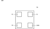
- FIG. 4 is a plan view of the variable capacitance device 91 as viewed from the mounting surface side.
- the variable capacitance device 91 of this embodiment is a one-chip element of CSP (ChipCSPsize package).
- Input / output terminals P1, P2, a control voltage input terminal Vt, and a ground terminal GND are arranged on the mounting surface of the chip.
- a ferroelectric thin film variable capacitor element VC is formed on the rewiring layer 50 provided on the main surface of the Si substrate 10, and the first input / output terminal, the second input / output terminal, and the ground are formed on the main surface of the semiconductor substrate.
- An ESD protection element connected between the terminals is formed.
- it is easy to ensure isolation between the variable capacitance element portion and the ESD protection element portion, and it is possible to configure a small variable capacitance device having excellent ESD resistance and high control sensitivity.
- a ferroelectric thin film variable capacitance device with an ESD protection element can be configured with one chip by a semiconductor manufacturing process.
- An electrode pad for connecting the ESD protection element to the ground terminal and the pair of input / output terminals is provided on the main surface of the semiconductor substrate, and the electrode pad is formed of W or WSi. Therefore, a ferroelectric thin film layer having high heat resistance of the pad electrode of the semiconductor substrate and requiring heat treatment at a high temperature can be incorporated into the rewiring layer.
- the variable capacitance element portion is provided at a position that does not overlap the ESD protection element and the electrode pad 13 in plan view. That is, the ESD protection element portion is not formed on the semiconductor substrate side of the variable capacitance element portion. Therefore, it is possible to ensure the flatness of the base portion of the variable capacitance element portion, and the coating thickness by spin coating of the BST film becomes uniform, so that a uniform and flat BST film can be formed, stable characteristics can be obtained, and the variable capacitance element The reliability of the department can be improved. Further, it becomes easier to secure isolation between the variable capacitance element portion and the ESD protection element portion.
- the resistance element portion RN connected between the variable capacitance element portion VC and the control voltage application terminal is formed on the mounting surface side of the rewiring layer 50 relative to the layer where the variable capacitance element portion VC is provided. Yes. Therefore, the flatness of the variable capacitance element portion is not adversely affected. Moreover, the isolation property between the ESD protection element portion and the resistance element can be improved.
- variable capacitance element portion VC and the semiconductor substrate 10 there are provided three insulating layers of the SiO 2 film 12, the SiN insulating film 14, and the BST film 21. That is, by forming a plurality of insulating layers between the semiconductor substrate 10 and the capacitor electrode 22, it is possible to further improve the isolation between the ESD protection part and the variable capacitance element part.
- the electrode pad may be formed of Mo or Pt.
- various semiconductor diodes using a semiconductor substrate such as a PN diode and a MOS diode can be used in addition to those using a Zener diode.
- 5A and 5B are cross-sectional views showing the structure and manufacturing method of the variable capacitance device 92 according to the second embodiment.
- the circuit diagram is the same as that shown in FIG. 1 in the first embodiment.
- variable capacitance device Accordingly, with reference to FIGS. 5A and 5B, the structure and the manufacturing method of the variable capacitance device according to the present embodiment will be described in order.
- An SiO 2 film 12 is formed on an N-type Si substrate 10, and an active region 11 by impurity diffusion is formed in an ESD protection element formation region by an ion implantation method or the like.
- the BST film and the Pt electrode film are alternately laminated on the SiO 2 film 12, and these are patterned to form the variable capacitance element portion VC. Further, the SiO 2 film 31 is formed by a CVD method or a sputtering SiO 2 film 12 surface.
- a PBO (polybenzoxazole) film is applied onto the SiO 2 film 31 by an automatic coater and baked to form a PBO film 32 as an organic protective layer.
- Openings H that reach the electrode film of the wiring pattern 42 and the variable capacitance element portion VC are formed by ICP-RIE.
- a Ti / Cu / Ti film is formed in the opening H and on the surface of the PBO film 32 by sputtering. As a result, a via 41 is formed in the opening H. Thereafter, the wiring pattern 45 is formed by patterning the Ti / Cu / Ti film on the surface of the PBO film 32.
- the terminal electrode 46 is formed by the same process as (6) onward in FIG. 3B.
- FIG. 6A and 6B are schematic views showing the element arrangement inside the variable capacitance device 92.
- FIG. 6A is a plan view
- FIG. 6B is a front view.
- the variable capacitance device 92 of the present embodiment is provided in a position where the variable capacitance element portion VC does not overlap with the ESD protection elements ESDP1 and ESDP2 and the electrode pads of the ESD protection elements in plan view.
- the resistance element portion RN connected between the variable capacitance element portion VC and the control voltage application terminal is formed on the mounting surface side of the rewiring layer 50 with respect to the layer provided with the variable capacitance element portion VC. ing.
- the wiring pattern is formed after the BST film of the variable capacitance element portion VC is baked, it is not necessary to use W (tungsten) for the electrode pad in contact with the active region 11, and the wiring pattern is Ti / Since Al can be used instead of Cu / Ti, the cost can be reduced.
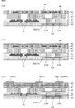
- FIG. 7 is a cross-sectional view of a variable capacitance device 93 according to the third embodiment.
- the variable capacitance device 93 includes a variable capacitance element portion VC, a resistance element portion RN, an ESD protection element ESDP2, and the like.
- 8A to 8E are cross-sectional views showing the structure of the variable capacitance device 93 and the manufacturing method thereof.
- variable capacitance device Accordingly, with reference to FIGS. 8A to 8E, the structure and the manufacturing method of the variable capacitance device according to the present embodiment will be described in order.
- An SiO 2 film 12P is formed on the N-type Si substrate 10, and active regions 11P and 11N by impurity diffusion are formed in the formation region of the ESD protection element of the Si substrate 10 by ion implantation or the like.
- An MIM layer in which BST films and Pt electrode films are alternately stacked is formed. These are formed by repeating a spin coating process and a baking process.
- variable capacitor element VC is formed by patterning the Pt electrode film and the BST film by photolithography over a predetermined number of times.
- the SiO 2 film 31 is formed by CVD or sputtering.
- Opening H is formed by ICP-RIE method.
- the electrode pad 13 is formed by sputtering and patterning Al.
- a PBO (polybenzoxazole) film is applied by an automatic coater and baked to form a PBO film 32 as an organic protective layer. Then, an opening H is formed in the PBO film 32 by the ICP-RIE method.
- Openings H are formed in the BST film on the upper surface of the SiO 2 film 31 and the variable capacitor element VC by the ICP-RIE method.
- a Ti / Cu / Ti film is formed in the opening H and on the surface of the PBO film 32 by sputtering. As a result, a via 41 is formed in the opening H. Thereafter, the wiring pattern 42 is formed by patterning the Ti / Cu / Ti film on the surface of the PBO film 32.
- a solder resist film 43 is formed on the surface of the PBO film 32, and an opening is formed at a predetermined position.
- a resistance element portion RN is formed by forming a NiCr / Si film on the surface of the solder resist film 43 and patterning it.
- a solder resist film 43 is formed, and an opening is formed at a predetermined position.
- a Ti / Cu / Ti film is formed on the surface of the solder resist film 43.
- the terminal electrode 46 is formed by forming and patterning an Au / Ni plating film.
- the wiring pattern 45 is formed by etching the Ti / Cu / Ti film.
- a solder resist film 47 is formed, and the terminal electrode 46 is opened.
- variable capacity device 93 shown in FIG. 7 is obtained by cutting the wafer into chips.
- the resistance element portion RN connected between the variable capacitance element portion VC and the control voltage application terminal is more mounted than the layer of the rewiring layer 50 in which the variable capacitance element portion VC is provided. And is formed in a region overlapping the formation region of the variable capacitance element portion VC and the ESD protection elements ESDP1 and ESDP2 in plan view. Therefore, a variable capacitance device with a small occupation area can be configured without adversely affecting the flatness of the variable capacitance element portion.
- the fourth embodiment shows a communication circuit including a variable capacitance device.
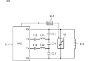
- FIG. 9 is a circuit diagram of a communication circuit including a variable capacitance device.
- This communication circuit is an example of an NFC module.
- the communication circuit includes an RFIC 111, an antenna coil 113, and a variable capacitance element device 91.
- the antenna coil 113 functions as a radiating element, and is magnetically coupled to the communication counterpart coil antenna.
- Capacitors C21 and C22 are elements for adjusting the degree of coupling between the RFIC 111 and the antenna coil 113.
- the inductors L11 and L12 and the capacitors C11, C12, and C20 constitute a transmission filter.
- a transmission filter For example, when the communication circuit operates in the card mode, since the RFIC 111 operates passively, a power supply voltage is generated from an input signal to the RX terminal, a received signal is read, and a circuit (load) connected to the TX terminal is transmitted during transmission. Modulate the load. For example, when the communication circuit operates in the reader / writer mode, the RFIC 111 operates in an active manner.
- the RX terminal is opened during transmission to transmit a transmission signal from the TX terminal, and the TX terminal is opened during reception to receive the RX terminal. Input the received signal.
- the RFIC 111 supplies a control voltage to the variable capacitance element device 91 via the DA converter 112. In this way, the impedance of the communication circuit as viewed from the RFIC 111 to the antenna coil 113 changes according to the operation mode.
- the capacitance value of the variable capacitive element device 91 is controlled so that the resonance frequency of the antenna circuit is optimized in accordance with the operation mode (so that the impedance when the antenna coil side is viewed from the RFIC 111 is matched).
- C1 Capacitance elements C11, C12, C20, C21, C22... Capacitors ESDP1, ESDP2... ESD protection element GND .. Ground terminal H .. Opening L11, L12. Inductor P1. ... terminal electrodes R11 to P19 ... RF resistance element RN ... resistance element part VC ... variable capacitance element part Vt ... control voltage input terminal 10 ... semiconductor substrate 11, 11P, 11N ... active region 12, 12P ... SiO 2 film 13 ... electrode pad 14 ... SiN insulating films 21, 23, 25 ... BST films 22, 24 ... Pt electrode films 31 ... SiO 2 films 32 ... PBO films 41, 44 ... vias 42, 45 ... wiring patterns 43, 47 ... solder resist films 46 ... terminals Electrode 50 ... Rewiring layers 91-93 ... Variable capacitance device 111 ... RFIC 112 ... DA converter 113 ... antenna coil
Abstract
Description
半導体基板と、その主面上に設けられた再配線層と、第1入出力端子、第2入出力端子およびグランド端子を含む複数の端子電極と、を有し、
前記再配線層に、第1入出力端子および第2入出力端子にそれぞれ接続された一対のキャパシタ電極と、一対のキャパシタ電極間に配置された強誘電体薄膜とで構成される強誘電体薄膜型の可変容量素子部が形成されており、
前記半導体基板に、第1入出力端子または第2入出力端子とグランド端子との間に接続されたESD保護素子が形成されている、ことを特徴とする。
半導体基板にESD保護素子を形成する工程と、
前記半導体基板の主面上に、一対のキャパシタ電極と一対のキャパシタ電極間に配置された強誘電体薄膜とで構成される強誘電体薄膜型の可変容量素子部を形成する工程と、
前記半導体基板の主面に可変容量素子部を覆う絶縁層を形成する工程と、
前記絶縁層に、ESD保護素子および可変容量素子部に接続された層間接続導体および端子電極を形成する工程と、を有する。
図1は第1の実施形態に係る可変容量デバイス91の回路図である。この可変容量デバイス91は、可変容量素子C1~C6、RF抵抗素子R11~R19およびESD保護素子ESDP1,ESDP2を含んでいる。
図5A、図5Bは第2の実施形態に係る可変容量デバイス92の構造および製造方法を示す断面図である。回路図は第1の実施形態で図1に示したものと同じである。
図7は第3の実施形態に係る可変容量デバイス93の断面図である。この可変容量デバイス93は、可変容量素子部VC、抵抗素子部RNおよびESD保護素子ESDP2等を含んでいる。図8A~図8Eは、可変容量デバイス93の構造および製造方法を示す断面図である。
第4の実施形態では可変容量デバイスを備えた通信回路について示す。
C11,C12,C20,C21,C22…キャパシタ
ESDP1,ESDP2…ESD保護素子
GND…グランド端子
H…開口
L11,L12…インダクタ
P1…第1入出力端子
P2…第2入出力端子
PE…端子電極
R11~P19…RF抵抗素子
RN…抵抗素子部
VC…可変容量素子部
Vt…制御電圧入力端子
10…半導体基板
11,11P,11N…活性領域
12,12P…SiO2膜
13…電極パッド
14…SiN絶縁膜
21,23,25…BST膜
22,24…Pt電極膜
31…SiO2膜
32…PBO膜
41,44…ビア
42,45…配線パターン
43,47…ソルダーレジスト膜
46…端子電極
50…再配線層
91~93…可変容量デバイス
111…RFIC
112…DAコンバータ
113…アンテナコイル
Claims (6)
- 半導体基板と、その主面上に設けられた再配線層と、第1入出力端子、第2入出力端子およびグランド端子を含む複数の端子電極と、を有し、
前記再配線層に、前記第1入出力端子および前記第2入出力端子にそれぞれ接続された一対のキャパシタ電極と、前記一対のキャパシタ電極間に配置された強誘電体薄膜とで構成される強誘電体薄膜型の可変容量素子部が形成されており、
前記半導体基板に、前記第1入出力端子または第2入出力端子と前記グランド端子との間に接続されたESD保護素子が形成されている、
ことを特徴とする、可変容量デバイス。 - 前記半導体基板の主面には、前記ESD保護素子を前記グランド端子と前記第1入出力端子または前記第2入出力端子とに接続するための電極パッドが設けられており、この電極パッドはWまたはWSiで形成されている、請求項1に記載の可変容量デバイス。
- 平面視で、前記可変容量素子部は、前記ESD保護素子および前記電極パッドと重ならない位置に設けられている、請求項2に記載の可変容量デバイス。
- 前記可変容量素子部と制御電圧印加端子との間に抵抗素子が設けられており、前記抵抗素子は、前記再配線層のうち、前記可変容量素子部が設けられた層に関して前記半導体基板とは反対側の層に形成されている、請求項1~3のいずれかに記載の可変容量デバイス。
- 前記可変容量素子部と前記半導体基板との間には絶縁層が設けられている、請求項1~4のいずれかに記載の可変容量デバイス。
- 半導体基板にESD保護素子を形成する工程と、
前記半導体基板の主面上に、一対のキャパシタ電極と前記一対のキャパシタ電極間に配置された強誘電体薄膜とで構成される強誘電体薄膜型の可変容量素子部を形成する工程と、
前記半導体基板の主面に前記可変容量素子部を覆う絶縁層を形成する工程と、
前記絶縁層に、前記ESD保護素子および前記可変容量素子部に接続された層間接続導体および端子電極を形成する工程と、
を有する、可変容量デバイスの製造方法。
Priority Applications (5)
| Application Number | Priority Date | Filing Date | Title |
|---|---|---|---|
| EP15772395.8A EP3128544B1 (en) | 2014-04-03 | 2015-03-17 | Variable capacitance device and production method therefor |
| JP2015534861A JP5812234B1 (ja) | 2014-04-03 | 2015-03-17 | 可変容量デバイス |
| CN201590000259.4U CN206134667U (zh) | 2014-04-03 | 2015-03-17 | 可变电容器 |
| US15/239,196 US9704847B2 (en) | 2014-04-03 | 2016-08-17 | Variable capacitance device |
| US15/611,855 US9991251B2 (en) | 2014-04-03 | 2017-06-02 | Semiconductor device |
Applications Claiming Priority (2)
| Application Number | Priority Date | Filing Date | Title |
|---|---|---|---|
| JP2014077102 | 2014-04-03 | ||
| JP2014-077102 | 2014-04-03 |
Related Child Applications (1)
| Application Number | Title | Priority Date | Filing Date |
|---|---|---|---|
| US15/239,196 Continuation US9704847B2 (en) | 2014-04-03 | 2016-08-17 | Variable capacitance device |
Publications (1)
| Publication Number | Publication Date |
|---|---|
| WO2015151786A1 true WO2015151786A1 (ja) | 2015-10-08 |
Family
ID=54240118
Family Applications (1)
| Application Number | Title | Priority Date | Filing Date |
|---|---|---|---|
| PCT/JP2015/057814 WO2015151786A1 (ja) | 2014-04-03 | 2015-03-17 | 可変容量デバイスおよびその製造方法 |
Country Status (5)
| Country | Link |
|---|---|
| US (2) | US9704847B2 (ja) |
| EP (1) | EP3128544B1 (ja) |
| JP (1) | JP5812234B1 (ja) |
| CN (1) | CN206134667U (ja) |
| WO (1) | WO2015151786A1 (ja) |
Cited By (7)
| Publication number | Priority date | Publication date | Assignee | Title |
|---|---|---|---|---|
| WO2018173522A1 (ja) * | 2017-03-22 | 2018-09-27 | 株式会社村田製作所 | 薄膜esd保護デバイス |
| CN110767626A (zh) * | 2018-07-26 | 2020-02-07 | 欣兴电子股份有限公司 | 封装结构及其制造方法 |
| JP6645639B1 (ja) * | 2019-02-22 | 2020-02-14 | 株式会社村田製作所 | 可変容量素子 |
| CN111180205A (zh) * | 2018-11-13 | 2020-05-19 | 罗姆股份有限公司 | 芯片电容器及芯片电容器的制造方法 |
| WO2020170481A1 (ja) * | 2019-02-22 | 2020-08-27 | 株式会社村田製作所 | 可変容量素子 |
| US11587734B2 (en) * | 2016-12-28 | 2023-02-21 | Murata Manufacturing Co., Ltd. | Thin-film device having a close-contact layer covering part of a wiring electrode, and method of manufacturing thin-film device |
| WO2023112551A1 (ja) * | 2021-12-17 | 2023-06-22 | ローム株式会社 | 半導体装置およびその製造方法 |
Families Citing this family (10)
| Publication number | Priority date | Publication date | Assignee | Title |
|---|---|---|---|---|
| JP5978969B2 (ja) * | 2012-12-07 | 2016-08-24 | 株式会社村田製作所 | 可変容量素子モジュール |
| JP5713150B2 (ja) * | 2013-03-29 | 2015-05-07 | 株式会社村田製作所 | 可変容量素子および通信装置 |
| WO2016021529A1 (ja) * | 2014-08-06 | 2016-02-11 | 株式会社村田製作所 | 複合電子部品 |
| JP6475198B2 (ja) * | 2016-06-29 | 2019-02-27 | 太陽誘電株式会社 | 可変容量デバイス及びアンテナ装置 |
| JP6406486B1 (ja) * | 2017-03-17 | 2018-10-17 | 株式会社村田製作所 | 薄膜esd保護デバイス |
| CN106960851B (zh) * | 2017-05-24 | 2020-02-21 | 京东方科技集团股份有限公司 | 阵列基板及其制作方法、显示面板和显示设备 |
| CN107346792B (zh) * | 2017-07-25 | 2020-01-10 | 上海华力微电子有限公司 | 一种用于闪存电路中的变容二极管结构及其制造方法 |
| US11121139B2 (en) * | 2017-11-16 | 2021-09-14 | International Business Machines Corporation | Hafnium oxide and zirconium oxide based ferroelectric devices with textured iridium bottom electrodes |
| EP3575262B1 (en) * | 2018-05-22 | 2021-04-14 | Murata Manufacturing Co., Ltd. | Reducing crosstalk in a mixed-signal multi-chip mems device package |
| JPWO2020085325A1 (ja) * | 2018-10-24 | 2021-09-09 | ソニーグループ株式会社 | カートリッジメモリおよびその制御方法、カートリッジならびに記録再生システム |
Citations (8)
| Publication number | Priority date | Publication date | Assignee | Title |
|---|---|---|---|---|
| JP2003229428A (ja) * | 2002-02-04 | 2003-08-15 | Matsushita Electric Ind Co Ltd | 半導体装置 |
| JP2008532308A (ja) * | 2005-03-02 | 2008-08-14 | エヌエックスピー ビー ヴィ | 電子デバイス及びその使用方法 |
| WO2011021411A1 (ja) * | 2009-08-21 | 2011-02-24 | 株式会社村田製作所 | Esd保護デバイス |
| US20120045881A1 (en) * | 2009-04-20 | 2012-02-23 | Nxp B.V. | Method for fabricating an integrated-passives device with a mim capacitor and a high-accuracy resistor on top |
| WO2013061985A1 (ja) * | 2011-10-26 | 2013-05-02 | 株式会社村田製作所 | 可変容量素子および高周波デバイス |
| JP2013214560A (ja) * | 2012-03-30 | 2013-10-17 | Tohoku Univ | 強誘電体容量を備えた集積回路基板の製造方法 |
| WO2013183472A1 (ja) * | 2012-06-08 | 2013-12-12 | 株式会社村田製作所 | 可変容量素子、高周波デバイスおよび通信装置 |
| JP2014036120A (ja) * | 2012-08-09 | 2014-02-24 | Dexerials Corp | 可変容量素子、実装回路、共振回路、通信装置、通信システム、ワイヤレス充電システム、電源装置、及び、電子機器 |
Family Cites Families (14)
| Publication number | Priority date | Publication date | Assignee | Title |
|---|---|---|---|---|
| US3569795A (en) * | 1969-05-29 | 1971-03-09 | Us Army | Voltage-variable, ferroelectric capacitor |
| US5438023A (en) * | 1994-03-11 | 1995-08-01 | Ramtron International Corporation | Passivation method and structure for a ferroelectric integrated circuit using hard ceramic materials or the like |
| KR100416733B1 (ko) * | 1995-03-20 | 2004-07-05 | 삼성전자주식회사 | 강유전성캐패시터 |
| US5706163A (en) * | 1995-11-28 | 1998-01-06 | California Micro Devices Corporation | ESD-protected thin film capacitor structures |
| JP2001326284A (ja) * | 2000-05-17 | 2001-11-22 | Nec Corp | 化合物半導体集積回路およびその製造方法 |
| JP4502609B2 (ja) | 2003-07-28 | 2010-07-14 | 京セラ株式会社 | 可変コンデンサ |
| TWI303542B (en) * | 2006-03-21 | 2008-11-21 | Ind Tech Res Inst | Film resistor embedded in a multiple-layer circuit board and manufacturing thereof |
| WO2008029361A1 (en) * | 2006-09-06 | 2008-03-13 | Nxp B.V. | Integrated circuit and use thereof |
| WO2008041565A1 (fr) | 2006-09-27 | 2008-04-10 | Kyocera Corporation | Condensateur, dispositif de condensateur, composant électronique, dispositif de filtre, dispositif de communication et procédé de fabrication d'un dispositif de condensateur |
| US7990749B2 (en) * | 2009-06-08 | 2011-08-02 | Radiant Technology, Inc. | Variable impedance circuit controlled by a ferroelectric capacitor |
| US10099614B2 (en) | 2011-11-28 | 2018-10-16 | Magna Electronics Inc. | Vision system for vehicle |
| KR101338286B1 (ko) * | 2012-04-03 | 2013-12-06 | 주식회사 하이딥 | 튜너블 커패시터 |
| JP2013258224A (ja) * | 2012-06-12 | 2013-12-26 | Taiyo Yuden Co Ltd | 可変容量コンデンサ素子 |
| US9595621B2 (en) * | 2015-03-30 | 2017-03-14 | Tdk Corporation | MOS capacitors flow type devices and methods of forming the same |
-
2015
- 2015-03-17 CN CN201590000259.4U patent/CN206134667U/zh active Active
- 2015-03-17 WO PCT/JP2015/057814 patent/WO2015151786A1/ja active Application Filing
- 2015-03-17 JP JP2015534861A patent/JP5812234B1/ja active Active
- 2015-03-17 EP EP15772395.8A patent/EP3128544B1/en active Active
-
2016
- 2016-08-17 US US15/239,196 patent/US9704847B2/en active Active
-
2017
- 2017-06-02 US US15/611,855 patent/US9991251B2/en active Active
Patent Citations (8)
| Publication number | Priority date | Publication date | Assignee | Title |
|---|---|---|---|---|
| JP2003229428A (ja) * | 2002-02-04 | 2003-08-15 | Matsushita Electric Ind Co Ltd | 半導体装置 |
| JP2008532308A (ja) * | 2005-03-02 | 2008-08-14 | エヌエックスピー ビー ヴィ | 電子デバイス及びその使用方法 |
| US20120045881A1 (en) * | 2009-04-20 | 2012-02-23 | Nxp B.V. | Method for fabricating an integrated-passives device with a mim capacitor and a high-accuracy resistor on top |
| WO2011021411A1 (ja) * | 2009-08-21 | 2011-02-24 | 株式会社村田製作所 | Esd保護デバイス |
| WO2013061985A1 (ja) * | 2011-10-26 | 2013-05-02 | 株式会社村田製作所 | 可変容量素子および高周波デバイス |
| JP2013214560A (ja) * | 2012-03-30 | 2013-10-17 | Tohoku Univ | 強誘電体容量を備えた集積回路基板の製造方法 |
| WO2013183472A1 (ja) * | 2012-06-08 | 2013-12-12 | 株式会社村田製作所 | 可変容量素子、高周波デバイスおよび通信装置 |
| JP2014036120A (ja) * | 2012-08-09 | 2014-02-24 | Dexerials Corp | 可変容量素子、実装回路、共振回路、通信装置、通信システム、ワイヤレス充電システム、電源装置、及び、電子機器 |
Non-Patent Citations (1)
| Title |
|---|
| See also references of EP3128544A4 * |
Cited By (13)
| Publication number | Priority date | Publication date | Assignee | Title |
|---|---|---|---|---|
| US11587734B2 (en) * | 2016-12-28 | 2023-02-21 | Murata Manufacturing Co., Ltd. | Thin-film device having a close-contact layer covering part of a wiring electrode, and method of manufacturing thin-film device |
| US11469593B2 (en) | 2017-03-22 | 2022-10-11 | Murata Manufacturing Co., Ltd. | Thin-film ESD protection device with compact size |
| JP6424994B1 (ja) * | 2017-03-22 | 2018-11-21 | 株式会社村田製作所 | 薄膜esd保護デバイス |
| WO2018173522A1 (ja) * | 2017-03-22 | 2018-09-27 | 株式会社村田製作所 | 薄膜esd保護デバイス |
| CN110767626A (zh) * | 2018-07-26 | 2020-02-07 | 欣兴电子股份有限公司 | 封装结构及其制造方法 |
| CN111180205A (zh) * | 2018-11-13 | 2020-05-19 | 罗姆股份有限公司 | 芯片电容器及芯片电容器的制造方法 |
| JP2020080384A (ja) * | 2018-11-13 | 2020-05-28 | ローム株式会社 | チップコンデンサおよびチップコンデンサの製造方法 |
| JP7150571B2 (ja) | 2018-11-13 | 2022-10-11 | ローム株式会社 | チップコンデンサおよびチップコンデンサの製造方法 |
| CN111180205B (zh) * | 2018-11-13 | 2021-10-22 | 罗姆股份有限公司 | 芯片电容器及芯片电容器的制造方法 |
| JP6645639B1 (ja) * | 2019-02-22 | 2020-02-14 | 株式会社村田製作所 | 可変容量素子 |
| US11107637B2 (en) | 2019-02-22 | 2021-08-31 | Murata Manufacturing Co., Ltd. | Variable capacitance element |
| WO2020170481A1 (ja) * | 2019-02-22 | 2020-08-27 | 株式会社村田製作所 | 可変容量素子 |
| WO2023112551A1 (ja) * | 2021-12-17 | 2023-06-22 | ローム株式会社 | 半導体装置およびその製造方法 |
Also Published As
| Publication number | Publication date |
|---|---|
| US20160351556A1 (en) | 2016-12-01 |
| US9991251B2 (en) | 2018-06-05 |
| EP3128544A4 (en) | 2018-01-17 |
| EP3128544B1 (en) | 2021-01-20 |
| US9704847B2 (en) | 2017-07-11 |
| JP5812234B1 (ja) | 2015-11-11 |
| JPWO2015151786A1 (ja) | 2017-04-13 |
| CN206134667U (zh) | 2017-04-26 |
| EP3128544A1 (en) | 2017-02-08 |
| US20170271318A1 (en) | 2017-09-21 |
Similar Documents
| Publication | Publication Date | Title |
|---|---|---|
| JP5812234B1 (ja) | 可変容量デバイス | |
| US9824955B2 (en) | Semiconductor device | |
| CN103891047B (zh) | 可变电容元件以及高频器件 | |
| JP5673865B2 (ja) | 通信装置 | |
| US9704799B2 (en) | Semiconductor device | |
| US10770451B2 (en) | Thin-film ESD protection device | |
| US9281557B2 (en) | Multi bandwidth balun and circuit structure thereof | |
| US10916378B2 (en) | Capacitance element having capacitance forming units arranged and electrically connected in series | |
| US20220320749A1 (en) | Semiconductor device, communication system, and method of manufacturing semiconductor device | |
| US11271283B2 (en) | Monolithically integrated antenna devices | |
| JP6424994B1 (ja) | 薄膜esd保護デバイス | |
| JP5978969B2 (ja) | 可変容量素子モジュール | |
| KR100838965B1 (ko) | 이동 전화 장치 | |
| US11069482B2 (en) | Capacitive element | |
| CN116544640A (zh) | 用于高频电流隔离器的电容耦合谐振器 |
Legal Events
| Date | Code | Title | Description |
|---|---|---|---|
| ENP | Entry into the national phase |
Ref document number: 2015534861 Country of ref document: JP Kind code of ref document: A |
|
| 121 | Ep: the epo has been informed by wipo that ep was designated in this application |
Ref document number: 15772395 Country of ref document: EP Kind code of ref document: A1 |
|
| REEP | Request for entry into the european phase |
Ref document number: 2015772395 Country of ref document: EP |
|
| WWE | Wipo information: entry into national phase |
Ref document number: 2015772395 Country of ref document: EP |
|
| NENP | Non-entry into the national phase |
Ref country code: DE |