WO2015146563A1 - セラミックスプレートと金属製の円筒部材との接合構造 - Google Patents
セラミックスプレートと金属製の円筒部材との接合構造 Download PDFInfo
- Publication number
- WO2015146563A1 WO2015146563A1 PCT/JP2015/056892 JP2015056892W WO2015146563A1 WO 2015146563 A1 WO2015146563 A1 WO 2015146563A1 JP 2015056892 W JP2015056892 W JP 2015056892W WO 2015146563 A1 WO2015146563 A1 WO 2015146563A1
- Authority
- WO
- WIPO (PCT)
- Prior art keywords
- flange
- bank
- ceramic plate
- gas introduction
- pipe
- Prior art date
- Legal status (The legal status is an assumption and is not a legal conclusion. Google has not performed a legal analysis and makes no representation as to the accuracy of the status listed.)
- Ceased
Links
Images

Classifications
-
- H—ELECTRICITY
- H10—SEMICONDUCTOR DEVICES; ELECTRIC SOLID-STATE DEVICES NOT OTHERWISE PROVIDED FOR
- H10P—GENERIC PROCESSES OR APPARATUS FOR THE MANUFACTURE OR TREATMENT OF DEVICES COVERED BY CLASS H10
- H10P72/00—Handling or holding of wafers, substrates or devices during manufacture or treatment thereof
- H10P72/70—Handling or holding of wafers, substrates or devices during manufacture or treatment thereof for supporting or gripping
- H10P72/72—Handling or holding of wafers, substrates or devices during manufacture or treatment thereof for supporting or gripping using electrostatic chucks
- H10P72/722—Details of electrostatic chucks
-
- B—PERFORMING OPERATIONS; TRANSPORTING
- B23—MACHINE TOOLS; METAL-WORKING NOT OTHERWISE PROVIDED FOR
- B23K—SOLDERING OR UNSOLDERING; WELDING; CLADDING OR PLATING BY SOLDERING OR WELDING; CUTTING BY APPLYING HEAT LOCALLY, e.g. FLAME CUTTING; WORKING BY LASER BEAM
- B23K1/00—Soldering, e.g. brazing, or unsoldering
- B23K1/19—Soldering, e.g. brazing, or unsoldering taking account of the properties of the materials to be soldered
-
- B—PERFORMING OPERATIONS; TRANSPORTING
- B23—MACHINE TOOLS; METAL-WORKING NOT OTHERWISE PROVIDED FOR
- B23K—SOLDERING OR UNSOLDERING; WELDING; CLADDING OR PLATING BY SOLDERING OR WELDING; CUTTING BY APPLYING HEAT LOCALLY, e.g. FLAME CUTTING; WORKING BY LASER BEAM
- B23K1/00—Soldering, e.g. brazing, or unsoldering
- B23K1/0008—Soldering, e.g. brazing, or unsoldering specially adapted for particular articles or work
-
- B—PERFORMING OPERATIONS; TRANSPORTING
- B23—MACHINE TOOLS; METAL-WORKING NOT OTHERWISE PROVIDED FOR
- B23K—SOLDERING OR UNSOLDERING; WELDING; CLADDING OR PLATING BY SOLDERING OR WELDING; CUTTING BY APPLYING HEAT LOCALLY, e.g. FLAME CUTTING; WORKING BY LASER BEAM
- B23K3/00—Tools, devices or special appurtenances for soldering, e.g. brazing, or unsoldering, not specially adapted for particular methods
-
- C—CHEMISTRY; METALLURGY
- C04—CEMENTS; CONCRETE; ARTIFICIAL STONE; CERAMICS; REFRACTORIES
- C04B—LIME, MAGNESIA; SLAG; CEMENTS; COMPOSITIONS THEREOF, e.g. MORTARS, CONCRETE OR LIKE BUILDING MATERIALS; ARTIFICIAL STONE; CERAMICS; REFRACTORIES; TREATMENT OF NATURAL STONE
- C04B37/00—Joining burned ceramic articles with other burned ceramic articles or other articles by heating
- C04B37/02—Joining burned ceramic articles with other burned ceramic articles or other articles by heating with metallic articles
- C04B37/023—Joining burned ceramic articles with other burned ceramic articles or other articles by heating with metallic articles characterised by the interlayer used
- C04B37/026—Joining burned ceramic articles with other burned ceramic articles or other articles by heating with metallic articles characterised by the interlayer used consisting of metals or metal salts
-
- H—ELECTRICITY
- H10—SEMICONDUCTOR DEVICES; ELECTRIC SOLID-STATE DEVICES NOT OTHERWISE PROVIDED FOR
- H10P—GENERIC PROCESSES OR APPARATUS FOR THE MANUFACTURE OR TREATMENT OF DEVICES COVERED BY CLASS H10
- H10P72/00—Handling or holding of wafers, substrates or devices during manufacture or treatment thereof
- H10P72/70—Handling or holding of wafers, substrates or devices during manufacture or treatment thereof for supporting or gripping
- H10P72/76—Handling or holding of wafers, substrates or devices during manufacture or treatment thereof for supporting or gripping using mechanical means, e.g. clamps or pinches
- H10P72/7604—Handling or holding of wafers, substrates or devices during manufacture or treatment thereof for supporting or gripping using mechanical means, e.g. clamps or pinches the wafers being placed on a susceptor, stage or support
- H10P72/7624—Handling or holding of wafers, substrates or devices during manufacture or treatment thereof for supporting or gripping using mechanical means, e.g. clamps or pinches the wafers being placed on a susceptor, stage or support characterised by the mechanical construction of the susceptor, stage or support
-
- B—PERFORMING OPERATIONS; TRANSPORTING
- B23—MACHINE TOOLS; METAL-WORKING NOT OTHERWISE PROVIDED FOR
- B23K—SOLDERING OR UNSOLDERING; WELDING; CLADDING OR PLATING BY SOLDERING OR WELDING; CUTTING BY APPLYING HEAT LOCALLY, e.g. FLAME CUTTING; WORKING BY LASER BEAM
- B23K2103/00—Materials to be soldered, welded or cut
- B23K2103/18—Dissimilar materials
-
- B—PERFORMING OPERATIONS; TRANSPORTING
- B23—MACHINE TOOLS; METAL-WORKING NOT OTHERWISE PROVIDED FOR
- B23K—SOLDERING OR UNSOLDERING; WELDING; CLADDING OR PLATING BY SOLDERING OR WELDING; CUTTING BY APPLYING HEAT LOCALLY, e.g. FLAME CUTTING; WORKING BY LASER BEAM
- B23K2103/00—Materials to be soldered, welded or cut
- B23K2103/50—Inorganic materials other than metals or composite materials
- B23K2103/52—Ceramics
-
- C—CHEMISTRY; METALLURGY
- C04—CEMENTS; CONCRETE; ARTIFICIAL STONE; CERAMICS; REFRACTORIES
- C04B—LIME, MAGNESIA; SLAG; CEMENTS; COMPOSITIONS THEREOF, e.g. MORTARS, CONCRETE OR LIKE BUILDING MATERIALS; ARTIFICIAL STONE; CERAMICS; REFRACTORIES; TREATMENT OF NATURAL STONE
- C04B2237/00—Aspects relating to ceramic laminates or to joining of ceramic articles with other articles by heating
- C04B2237/02—Aspects relating to interlayers, e.g. used to join ceramic articles with other articles by heating
- C04B2237/12—Metallic interlayers
- C04B2237/121—Metallic interlayers based on aluminium
-
- C—CHEMISTRY; METALLURGY
- C04—CEMENTS; CONCRETE; ARTIFICIAL STONE; CERAMICS; REFRACTORIES
- C04B—LIME, MAGNESIA; SLAG; CEMENTS; COMPOSITIONS THEREOF, e.g. MORTARS, CONCRETE OR LIKE BUILDING MATERIALS; ARTIFICIAL STONE; CERAMICS; REFRACTORIES; TREATMENT OF NATURAL STONE
- C04B2237/00—Aspects relating to ceramic laminates or to joining of ceramic articles with other articles by heating
- C04B2237/02—Aspects relating to interlayers, e.g. used to join ceramic articles with other articles by heating
- C04B2237/12—Metallic interlayers
- C04B2237/124—Metallic interlayers based on copper
-
- C—CHEMISTRY; METALLURGY
- C04—CEMENTS; CONCRETE; ARTIFICIAL STONE; CERAMICS; REFRACTORIES
- C04B—LIME, MAGNESIA; SLAG; CEMENTS; COMPOSITIONS THEREOF, e.g. MORTARS, CONCRETE OR LIKE BUILDING MATERIALS; ARTIFICIAL STONE; CERAMICS; REFRACTORIES; TREATMENT OF NATURAL STONE
- C04B2237/00—Aspects relating to ceramic laminates or to joining of ceramic articles with other articles by heating
- C04B2237/02—Aspects relating to interlayers, e.g. used to join ceramic articles with other articles by heating
- C04B2237/12—Metallic interlayers
- C04B2237/125—Metallic interlayers based on noble metals, e.g. silver
-
- C—CHEMISTRY; METALLURGY
- C04—CEMENTS; CONCRETE; ARTIFICIAL STONE; CERAMICS; REFRACTORIES
- C04B—LIME, MAGNESIA; SLAG; CEMENTS; COMPOSITIONS THEREOF, e.g. MORTARS, CONCRETE OR LIKE BUILDING MATERIALS; ARTIFICIAL STONE; CERAMICS; REFRACTORIES; TREATMENT OF NATURAL STONE
- C04B2237/00—Aspects relating to ceramic laminates or to joining of ceramic articles with other articles by heating
- C04B2237/02—Aspects relating to interlayers, e.g. used to join ceramic articles with other articles by heating
- C04B2237/12—Metallic interlayers
- C04B2237/126—Metallic interlayers wherein the active component for bonding is not the largest fraction of the interlayer
- C04B2237/127—The active component for bonding being a refractory metal
-
- C—CHEMISTRY; METALLURGY
- C04—CEMENTS; CONCRETE; ARTIFICIAL STONE; CERAMICS; REFRACTORIES
- C04B—LIME, MAGNESIA; SLAG; CEMENTS; COMPOSITIONS THEREOF, e.g. MORTARS, CONCRETE OR LIKE BUILDING MATERIALS; ARTIFICIAL STONE; CERAMICS; REFRACTORIES; TREATMENT OF NATURAL STONE
- C04B2237/00—Aspects relating to ceramic laminates or to joining of ceramic articles with other articles by heating
- C04B2237/30—Composition of layers of ceramic laminates or of ceramic or metallic articles to be joined by heating, e.g. Si substrates
- C04B2237/32—Ceramic
- C04B2237/36—Non-oxidic
- C04B2237/366—Aluminium nitride
-
- C—CHEMISTRY; METALLURGY
- C04—CEMENTS; CONCRETE; ARTIFICIAL STONE; CERAMICS; REFRACTORIES
- C04B—LIME, MAGNESIA; SLAG; CEMENTS; COMPOSITIONS THEREOF, e.g. MORTARS, CONCRETE OR LIKE BUILDING MATERIALS; ARTIFICIAL STONE; CERAMICS; REFRACTORIES; TREATMENT OF NATURAL STONE
- C04B2237/00—Aspects relating to ceramic laminates or to joining of ceramic articles with other articles by heating
- C04B2237/30—Composition of layers of ceramic laminates or of ceramic or metallic articles to be joined by heating, e.g. Si substrates
- C04B2237/40—Metallic
- C04B2237/405—Iron metal group, e.g. Co or Ni
- C04B2237/406—Iron, e.g. steel
-
- C—CHEMISTRY; METALLURGY
- C04—CEMENTS; CONCRETE; ARTIFICIAL STONE; CERAMICS; REFRACTORIES
- C04B—LIME, MAGNESIA; SLAG; CEMENTS; COMPOSITIONS THEREOF, e.g. MORTARS, CONCRETE OR LIKE BUILDING MATERIALS; ARTIFICIAL STONE; CERAMICS; REFRACTORIES; TREATMENT OF NATURAL STONE
- C04B2237/00—Aspects relating to ceramic laminates or to joining of ceramic articles with other articles by heating
- C04B2237/50—Processing aspects relating to ceramic laminates or to the joining of ceramic articles with other articles by heating
- C04B2237/80—Joining the largest surface of one substrate with a smaller surface of the other substrate, e.g. butt joining or forming a T-joint
Definitions
- the present invention relates to a joint structure between a ceramic plate and a metal cylindrical member.
- the electrostatic chuck is used as a holding member for adsorbing a wafer and controlling the temperature of the wafer during the semiconductor manufacturing process.
- a metal gas introduction pipe is joined from the back side of a disk-shaped ceramic plate provided with a gas introduction hole, and He gas is supplied to the adsorption surface of the wafer to conduct heat.
- the thing which improved the property is known (for example, patent document 1).
- a brazing material is filled between the ceramic plate 110 and the gas introduction pipe 120 and the side surface of the gas introduction pipe 120 is used.
- a method of brazing by applying a brazing material over the back surface of an electrostatic chuck is known (for example, Patent Document 2). After brazing, the brazing material becomes a fillet-like brazed portion 124.
- a stress due to a difference in thermal expansion is generated between the ceramic plate 110 and the gas introduction pipe 120.
- the gas introduction pipe 120 is formed of a metal having a thermal expansion coefficient close to that of the ceramic plate 110. ing.
- the gas introduction pipe 120 is formed of a metal having a thermal expansion coefficient close to that of the ceramic plate 110 in the joining structure of FIG. 7, if the thermal cycle is applied when the electrostatic chuck is used, the joint may peel off. there were. The cause is that the gas introduction pipe 120 and the brazing part 124 contract more than the ceramic plate 110 during cooling. For this reason, the ceramic plate 110 is cracked only by repeating the thermal cycle several times, the airtightness cannot be maintained, and a leak may occur from the gas introduction hole.
- a metal ring (not shown) having a slightly smaller diameter than the ceramic plate 110 may be brazed to the back surface of the ceramic plate 110. Even at the joint with 110, there was a problem that cracks occurred and the airtightness could not be maintained as described above.
- the present invention has been made to solve such a problem, and it is a main object of the present invention to improve durability against thermal cycling in a joining structure of a ceramic plate and a metal cylindrical member.
- the joint structure of the present invention is It is a joining structure of a ceramic plate and a metal cylindrical member, A flange formed at an end of the cylindrical member; An annular bank provided at a position facing the flange of the ceramic plate; A brazed portion formed between the flange and the bank; With The flange has a width of 3 mm or more and a thickness of 0.5 mm or more and 2 mm or less, The bank has a chamfered corner or a chamfered corner facing the outer edge of the flange. Is.
- the flange of the cylindrical member and the annular bank of the ceramic plate are joined by a brazing portion.
- the size and thickness of the flange are in an appropriate numerical range, and the bank is chamfered or rounded at the corner facing the outer edge of the flange. Therefore, the stress due to the difference in thermal expansion between the cylindrical member and the ceramic plate can be received by the side surface of the bank, and the structure is strong against the stress. Further, the bonding area is increased and the sealing distance is increased. Therefore, even if the thermal cycle is repeatedly performed on the joined body having such a joined structure, the occurrence of cracks at the joined portion can be suppressed. Therefore, according to such a joint structure, durability against thermal cycling is improved.
- the bank preferably has a height of 0.5 mm or more. In this way, durability against thermal cycling is further improved.
- the bank is preferably C0.3 or more when the chamfering of the corner facing the outer edge of the flange is C chamfering, and is R0.3 or more in the case of R chamfering. It is preferable. In this way, durability against thermal cycling is further improved.
- the ceramic plate is made of AlN
- the cylindrical member is made of Kovar
- the brazing portion is formed of a brazing material containing Ag, Cu and Ti or Al brazing. It is preferable. If such a combination of materials is employed, the effects of the present invention can be obtained more reliably.
- the ceramic plate has a gas introduction hole that opens to the inside of the annular bank and penetrates in the thickness direction, and the cylindrical member supplies a gas to the gas introduction hole. It is good. In this way, it is possible to prevent the gas supplied from the gas introduction pipe from leaking outside the gas introduction pipe or the gas introduction hole even after the thermal cycle.
- the annular bank may be formed along an outer peripheral edge of the ceramic plate, and the cylindrical member may be a support ring that supports the ceramic plate. In this way, the airtightness inside the support ring can be maintained even after the thermal cycle.
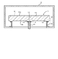
- Sectional drawing which shows schematic structure of the member 1 for semiconductor manufacturing apparatuses.
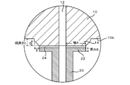
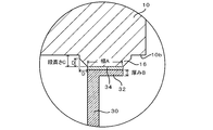
- the A section enlarged view of FIG. The B section enlarged view of FIG.
- FIG. 1 is a sectional view showing a schematic configuration of a member 1 for a semiconductor manufacturing apparatus
- FIG. 2 is an enlarged view of a portion A in FIG. 1
- FIG. 3 is an enlarged view of a portion B in FIG.
- the semiconductor manufacturing apparatus member 1 is installed inside a chamber 2 as shown in FIG.
- the semiconductor manufacturing apparatus member 1 includes a susceptor 10 having a wafer mounting surface 10a on which a wafer W is mounted, and a small diameter gas bonded to a back surface 10b of the susceptor 10 opposite to the wafer mounting surface 10a.
- An introduction pipe 20 and a large-diameter support ring 30 joined to the back surface 10b are provided.
- the semiconductor manufacturing apparatus member 1 is joined to the inner surface of the chamber 2 at the lower end of the support ring 30 so as to be airtight.
- the susceptor 10 is a disc-shaped AlN ceramic plate.
- the susceptor 10 includes a gas introduction hole 12 that penetrates in the thickness direction.
- An annular pipe joining bank 14 is formed around the opening on the back surface 10 b side of the gas introduction hole 12.
- the pipe joining bank 14 is provided at a position facing the flange 22 of the gas introduction pipe 20.
- An annular ring bonding bank 16 is formed at a position facing the flange 32 of the support ring 30 in the susceptor 10.
- the ring bonding bank 16 is formed slightly inside the outer periphery of the susceptor 10 and along the outer periphery.
- the gas introduction pipe 20 is made of Kovar, and has a flange 22 at the end joined to the back surface 10b of the susceptor 10, as shown in FIG.
- Kovar has a thermal expansion coefficient equivalent to that of AlN.
- the thermal expansion coefficient of AlN is 4.3 ⁇ 10 ⁇ 6 / ° C. (40 ° C. to 400 ° C.)
- the thermal expansion coefficient of Kovar is 9 ⁇ 10 ⁇ 6 / ° C. (40 ° C. to 400 ° C.).
- a pipe brazing portion 24 is formed between the flange 22 and the pipe joining bank 14.
- the pipe brazing portion 24 is made of, for example, Ag—Cu—Ti brazing material or Al brazing.
- the thermal expansion coefficient of the Ag—Cu—Ti brazing material is 18.5 ⁇ 10 ⁇ 6 / ° C. (40 ° C. to 400 ° C.) when the composition is 63 wt% Ag, 32.25 wt% Cu and 1.75 wt% Ti.
- the thermal expansion coefficient of Al brazing is 19.5 ⁇ 10 ⁇ 6 / ° C. (40 ° C. to 400 ° C.).
- the support ring 30 is made of Kovar, and has a flange 32 at the end joined to the back surface 10b of the susceptor 10 as shown in FIG.
- the diameter of the support ring 30 is slightly smaller than the diameter of the susceptor 10.
- a ring brazing portion 34 is formed between the flange 32 and the ring bonding bank 16.
- the ring brazing portion 34 is made of, for example, Ag—Cu—Ti brazing material or Al brazing.
- the flanges 22 and 32 have a width A of 3 mm or more and a thickness B of 0.5 mm or more and 2 mm or less. If the width A of the flanges 22 and 32 is less than 3 mm, it is not preferable because the airtightness cannot be maintained due to insufficient sealing distance or insufficient bonding area. On the other hand, when the thickness B of the flanges 22 and 32 exceeds 2 mm, the stress generated in the joint portion during the thermal cycle becomes too large and cracks are formed in the joint portion. Considering the magnitude of this stress, the thinner the flanges 22 and 32, the better. However, when the thickness is less than 0.5 mm, it is not preferable because the manufacturing becomes difficult.
- the pipe joining bank 14 and the ring joining bank 16 preferably have a step height C of 0.5 mm or more, and chamfered corners facing the outer edges of the flanges 22 and 32.
- the size D is C chamfering, it is preferably C0.3 or more, and when R is chamfering, it is preferably R0.3 or more. If this condition is satisfied, the durability against thermal cycling is sufficiently high. 2 and 3, the corner chamfering of each of the banks 14 and 16 is exemplified as the C chamfering.
- each bank 14 and 16 is less than 0.5 mm, the durability against thermal cycling is improved as compared with the case where each bank 14 and 16 is not provided. Further, even when the corner chamfer size D of each bank 14 and 16 is less than C0.3 when the chamfer is chamfered and less than R0.3 when the chamfer is chamfered, compared to the case where the corner is not chamfered. Durability against thermal cycling is improved.
- the semiconductor manufacturing apparatus member 1 is disposed in the chamber 2 and is used for etching the surface of the wafer W by the plasma generated in the chamber 2. At this time, if necessary, He gas is supplied to the back surface of the wafer W through the gas introduction pipe 20 and the gas introduction hole 12. Thereby, the thermal uniformity of the wafer W is improved.
- the susceptor 10 of this embodiment corresponds to the ceramic plate of the present invention
- the gas introduction pipe 20 and the support ring 30 each correspond to a cylindrical member.
- the flange 22 of the gas introduction pipe 20 and the pipe joining bank 14 of the susceptor 10 are joined by the pipe brazing portion 24, and the flange 22 of the support ring 30 is
- the ring bonding bank 16 of the susceptor 10 is bonded to the ring brazing portion 34.
- the sizes and thicknesses of the flanges 22 and 32 are in an appropriate numerical range, and the banks 14 and 16 are chamfered or rounded at the corners facing the outer edges of the flanges 22 and 32. Therefore, the stress due to the difference in thermal expansion between the support ring 30 and the susceptor 10 can be received on the side surfaces of the banks 14 and 16, and the structure is strong against the stress.
- the bonding area is increased and the sealing distance is increased. Therefore, even if the thermal cycle is repeatedly performed on the semiconductor manufacturing apparatus member 1 having such a bonded structure, it is possible to suppress the occurrence of cracks at the bonded portion. Therefore, according to this member 1 for semiconductor manufacturing equipment, durability against thermal cycling is improved.
- the susceptor 10 is made of AlN
- the gas introduction pipe 20 and the support ring 30 are made of Kovar
- the pipe brazing portion 24 and the ring brazing portion 34 are made of Ag—Cu—Ti brazing material or Al brazing. Since it is formed, the stress generated by the difference in thermal expansion can be kept low, and the durability against thermal cycling can be reliably increased.
- a ceramic plate in which at least one of an electrostatic electrode, a heater electrode, and a plasma generating electrode is embedded may be used.
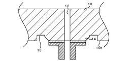
- the pipe joining bank 14 is provided so as to protrude from the back surface 10b of the susceptor 10.
- the circumferential groove 13 is formed around the opening of the gas introduction hole 12 in the back surface 10b. It may be provided to form the pipe joining bank 14.
- the height of the top surface of the pipe joining bank 14 is the same as the height of the back surface 10b. Even if it does in this way, the effect similar to embodiment mentioned above is acquired.
- the ring bonding bank 16 may be formed in the same manner. That is, a small-diameter circumferential groove and a large-diameter circumferential groove may be provided, and the ring joining bank 16 may be formed between the both grooves.
- AlN is adopted as the material of the susceptor 10, but ceramics other than AlN (for example, alumina or the like) may be adopted.
- the material of the gas introduction pipe 20 and the support ring 30 is the same as that of the material of the susceptor 10 (for example, a material having a thermal expansion coefficient of ⁇ 10% of the material of the susceptor 10).
- the brazing material of the pipe brazing part 24 and the ring brazing part 34 also has the same thermal expansion coefficient as the material of the susceptor 10.
- the gas introduction pipe 20 and the support ring 30 are exemplified as the metal cylindrical member, but other cylindrical members may be joined.
- a cylindrical member for inserting a thermocouple for measuring the surface temperature of the susceptor 10 may be joined.
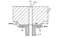
- a test sample shown in FIG. 5 was produced. That is, first, an AlN block 50 imitating the susceptor 10 was prepared. The block 50 is provided with a gas introduction hole 52 simulating the gas introduction hole 12 and a pipe joining bank 54 simulating the pipe joining bank 14. Then, the flange 22 of the gas introduction pipe 20 made of Kovar was joined to the pipe joining bank 54 via the pipe brazing portion 24 to obtain a test sample.
- As the brazing material an Ag—Cu—Ti brazing material (Ag 63 wt%, Cu 32.25 wt%, Ti 1.75 wt%) was used.
- the gas introduction pipe 20 having an inner diameter of about 7.5 mm and an outer diameter of about 9.5 mm was used.
- sample Nos. Having the flange width A, flange thickness B, bank step height C, and chamfer size D shown in Table 1 were used. 1 to 16 were produced.
- the leak amount is a threshold value (here, 1 ⁇ 10 ⁇ 8 Pa ⁇ m 3 / If it was less than sec), it was determined that the sealing property was good, and if it was equal to or greater than the threshold value, it was determined that the sealing property was poor.
- a threshold value here, 1 ⁇ 10 ⁇ 8 Pa ⁇ m 3 / If it was less than sec
- the sealing property was good and there was no crack in cross-sectional observation it was evaluated as “OK”, and when the sealing property was poor or there was a crack in cross-sectional observation, it was evaluated as “NG”.
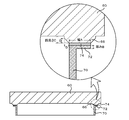
- a test sample shown in FIG. 6 was produced. That is, first, an AlN plate 60 imitating the susceptor 10 and a Kovar ring 70 imitating the support ring 30 were prepared. The plate 60 is provided with a ring joining bank 66 simulating the ring joining bank 16, and the ring 70 is provided with a flange 72 simulating the flange 32. Then, the flange 72 of the ring 70 was joined to the ring joining bank 66 via the ring brazing portion 74 to obtain a test sample. As the brazing material, the above-described Ag—Cu—Ti brazing material was used.
- the ring 70 having an inner diameter of about 228 mm and an outer diameter of about 229.5 mm was used.
- sample Nos. sample Nos. Having the flange width A, the flange thickness B, the bank step height C, and the chamfer size D shown in Table 2 were used. 17 to 24 were produced.
- Sample No. Sample Nos. 17-24 Evaluation was carried out in the same manner as in 1 to 16, and the results are shown in Table 2.
- the present invention can be used as a member for a semiconductor manufacturing apparatus such as an electrostatic chuck, an electrostatic chuck heater, or a ceramic heater.
- SYMBOLS 1 Member for semiconductor manufacturing apparatuses 2 chamber, 10 susceptor, 10a wafer mounting surface, 10b back surface, 12 gas introduction hole, 13 circumferential groove, 14 pipe joining bank, 16 ring joining bank, 20 gas introduction pipe, 22 Flange, 24 pipe brazed part, 30 support ring, 32 flange, 34 ring brazed part, 50 block, 52 gas introduction hole, 52a opening, 54 pipe joining bank, 60 plate, 66 ring joining bank, 70 ring, 72 flange, 74 ring brazed part, 110 ceramics plate, 120 gas introduction pipe, 124 brazed part.
Landscapes
- Engineering & Computer Science (AREA)
- Chemical & Material Sciences (AREA)
- Ceramic Engineering (AREA)
- Materials Engineering (AREA)
- Mechanical Engineering (AREA)
- Structural Engineering (AREA)
- Organic Chemistry (AREA)
- Container, Conveyance, Adherence, Positioning, Of Wafer (AREA)
- Ceramic Products (AREA)
Abstract
Description
セラミックスプレートと金属製の円筒部材との接合構造であって、
前記円筒部材の端部に形成されたフランジと、
前記セラミックスプレートのうち前記フランジと対向する位置に設けられた環状のバンクと、
前記フランジと前記バンクとの間に形成されたろう付け部と、
を備え、
前記フランジは、幅が3mm以上、厚みが0.5mm以上2mm以下であり、
前記バンクは、前記フランジの外縁に対向する角の面取りがC面取り又はR面取りされている、
ものである。
図5に示す試験用サンプルを作製した。すなわち、まず、サセプタ10を模したAlN製のブロック50を用意した。ブロック50には、ガス導入孔12を模したガス導入孔52と、パイプ接合用バンク14を模したパイプ接合用バンク54とを設けた。そして、パイプ接合用バンク54に、パイプろう付け部24を介してコバール製のガス導入パイプ20のフランジ22を接合し、試験用サンプルとした。ろう材は、Ag-Cu-Tiろう材(Ag63重量%、Cu32.25重量%、Ti1.75重量%)を使用した。ガス導入パイプ20は、内径が約7.5mm、外径が約9.5mmのものを使用した。試験用サンプルとしては、表1に示すフランジ幅A、フランジ厚みB、バンクの段高さC、面取りサイズDを有するサンプルNo.1~16を作製した。
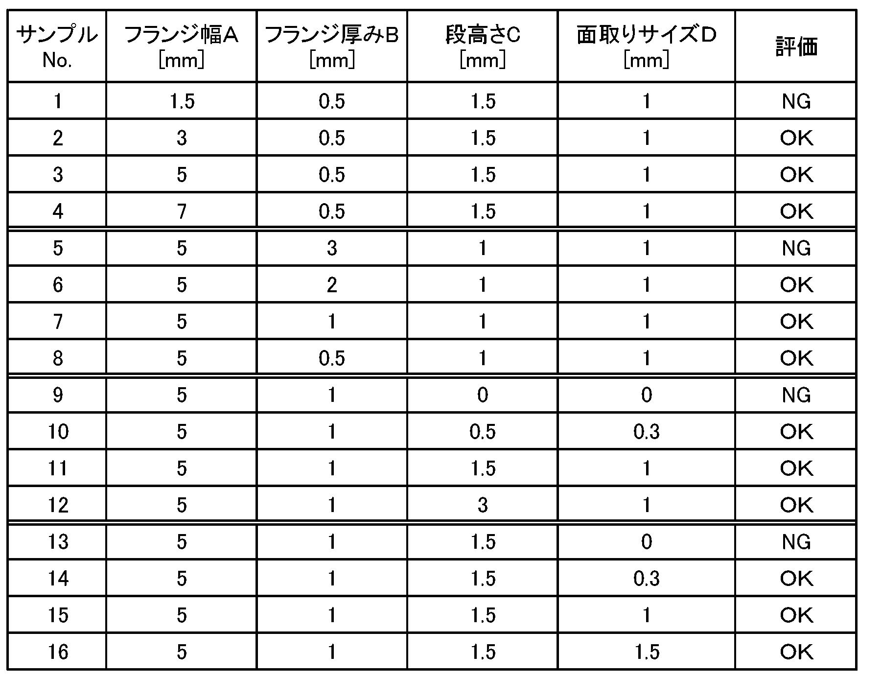
各サンプルを熱サイクル試験に供した。熱サイクル試験は、大気中で150℃から450℃に昇温し、その後150℃に降温するのを1サイクルとし、これを50サイクル行った。熱サイクル試験後、接合部のシール性の確認と、断面観察によるクラックの確認を行った。接合部のシール性の確認は、ガス導入孔52の開口52aを塞ぎ、ガス導入パイプ20の入口からHeリークディテクタを用いて真空引きを行い、接合部側面からHeを吹き付けてHeのリーク量を測定した。リーク量が閾値(ここでは1×10⁻⁸Pa・m3/
sec)未満であればシール性良好と判定し、閾値以上であればシール性不良と判断した。そして、シール性が良好で且つ断面観察でクラックなしの場合、「OK」と評価し、シール性が不良か断面観察でクラックありの場合、「NG」と評価した。その結果を表1に示した。
図6に示す試験用サンプルを作製した。すなわち、まず、サセプタ10を模したAlN製のプレート60と、支持リング30を模したコバール製のリング70とを用意した。プレート60には、リング接合用バンク16を模したリング接合用バンク66を設け、リング70には、フランジ32を模したフランジ72を設けた。そして、リング接合用バンク66に、リングろう付け部74を介してリング70のフランジ72を接合し、試験用サンプルとした。ろう材は、上述したAg-Cu-Tiろう材を使用した。また、リング70のサイズは、内径が約228mm、外径が約229.5mmのものを使用した。試験用サンプルとしては、表2に示すフランジ幅A、フランジ厚みB、バンクの段高さC、面取りサイズDを有するサンプルNo.17~24を作製した。

サンプルNo.17~24についても、サンプルNo.1~16と同様にして評価を行い、その結果を表2に示した。サンプルNo.17,18の評価結果から、フランジ幅Aは3mm以上であれば、接合面積が十分広くシール距離も十分長くなるため、シール性が良好でクラックも見られなかった。サンプルNo.19,20の評価結果から、フランジ厚みBは2mm以下であれば、熱サイクル試験中に大きな応力が発生しないため、シール性が良好でクラックも見られなかった。サンプルNo.21,22の評価結果から、リング接合用バンクの段高さCが0.5mm以上であれば、熱サイクル試験中に発生する応力が緩和されるため、シール性が良好でクラックも見られなかった。サンプルNo.23,24の評価結果から、面取りサイズD(ここではC面取り)が0.3mm以上(つまりC0.3以上)であれば、熱サイクル試験中に発生する応力が緩和されるため、シール性が良好でクラックも見られなかった。また、C面取りの代わりにR面取りを行った場合も、同様の結果が得られた。
Claims (6)
- セラミックスプレートと金属製の円筒部材との接合構造であって、
前記円筒部材の端部に形成されたフランジと、
前記セラミックスプレートのうち前記フランジと対向する位置に設けられた環状のバンクと、
前記フランジと前記バンクとの間に形成されたろう付け部と、
を備え、
前記フランジは、幅が3mm以上、厚みが0.5mm以上2mm以下であり、
前記バンクは、前記フランジの外縁に対向する角の面取りがC面取り又はR面取りされている、
接合構造。 - 前記バンクは、高さが0.5mm以上である、
請求項1に記載の接合構造。 - 前記バンクは、前記フランジの外縁に対向する角の面取りがC面取りの場合にはC0.3以上、R面取りの場合にはR0.3以上である、
請求項1又は2に記載の接合構造。 - 前記セラミックスプレートは、AlN製であり、
前記円筒部材は、コバール製であり、
前記ろう付け部は、Ag,Cu及びTiを含むろう材又はAlろうによって形成されている、
請求項1~3のいずれか1項に記載の接合構造。 - 前記セラミックスプレートは、前記環状のバンクの内側に開口し厚み方向に貫通するガス導入孔を有し、
前記円筒部材は、前記ガス導入孔へガスを供給するガス導入パイプである、
請求項1~4のいずれか1項に記載の接合構造。 - 前記環状のバンクは、前記セラミックスプレートの外周縁に沿って形成され、
前記円筒部材は、前記セラミックスプレートを支持する支持リングである、
請求項1~4のいずれか1項に記載の接合構造。
Priority Applications (4)
| Application Number | Priority Date | Filing Date | Title |
|---|---|---|---|
| JP2015544246A JP5851665B1 (ja) | 2014-03-27 | 2015-03-10 | セラミックスプレートと金属製の円筒部材との接合構造 |
| CN201580001225.1A CN105392758B (zh) | 2014-03-27 | 2015-03-10 | 陶瓷板与金属制圆筒部件的接合结构 |
| KR1020157036810A KR101658749B1 (ko) | 2014-03-27 | 2015-03-10 | 세라믹스 플레이트와 금속제 원통 부재의 접합 구조 |
| US14/964,977 US9583372B2 (en) | 2014-03-27 | 2015-12-10 | Structure for joining ceramic plate to metal cylindrical member |
Applications Claiming Priority (2)
| Application Number | Priority Date | Filing Date | Title |
|---|---|---|---|
| JP2014-065541 | 2014-03-27 | ||
| JP2014065541 | 2014-03-27 |
Related Child Applications (1)
| Application Number | Title | Priority Date | Filing Date |
|---|---|---|---|
| US14/964,977 Continuation US9583372B2 (en) | 2014-03-27 | 2015-12-10 | Structure for joining ceramic plate to metal cylindrical member |
Publications (1)
| Publication Number | Publication Date |
|---|---|
| WO2015146563A1 true WO2015146563A1 (ja) | 2015-10-01 |
Family
ID=54195088
Family Applications (1)
| Application Number | Title | Priority Date | Filing Date |
|---|---|---|---|
| PCT/JP2015/056892 Ceased WO2015146563A1 (ja) | 2014-03-27 | 2015-03-10 | セラミックスプレートと金属製の円筒部材との接合構造 |
Country Status (6)
| Country | Link |
|---|---|
| US (1) | US9583372B2 (ja) |
| JP (1) | JP5851665B1 (ja) |
| KR (1) | KR101658749B1 (ja) |
| CN (1) | CN105392758B (ja) |
| TW (1) | TWI538764B (ja) |
| WO (1) | WO2015146563A1 (ja) |
Cited By (6)
| Publication number | Priority date | Publication date | Assignee | Title |
|---|---|---|---|---|
| JP2017153254A (ja) * | 2016-02-25 | 2017-08-31 | 京セラ株式会社 | 半導体製造装置用部品 |
| JP2017191910A (ja) * | 2016-04-15 | 2017-10-19 | 日本特殊陶業株式会社 | 基板保持装置及びその製造方法 |
| JP2021153142A (ja) * | 2020-03-24 | 2021-09-30 | 東京エレクトロン株式会社 | 基板載置台及び基板処理装置 |
| JP2023023729A (ja) * | 2021-08-06 | 2023-02-16 | 国立研究開発法人産業技術総合研究所 | 接合体の製造方法および接合体 |
| US11945755B2 (en) | 2018-11-30 | 2024-04-02 | Kyocera Corporation | Ceramic structure and structure with terminal |
| JP2024065891A (ja) * | 2022-10-31 | 2024-05-15 | 日本特殊陶業株式会社 | セラミックスヒーター |
Families Citing this family (5)
| Publication number | Priority date | Publication date | Assignee | Title |
|---|---|---|---|---|
| US9738975B2 (en) * | 2015-05-12 | 2017-08-22 | Lam Research Corporation | Substrate pedestal module including backside gas delivery tube and method of making |
| JP6615134B2 (ja) * | 2017-01-30 | 2019-12-04 | 日本碍子株式会社 | ウエハ支持台 |
| US10147610B1 (en) | 2017-05-30 | 2018-12-04 | Lam Research Corporation | Substrate pedestal module including metallized ceramic tubes for RF and gas delivery |
| CN113170536B (zh) * | 2019-01-25 | 2023-06-09 | 日本碍子株式会社 | 陶瓷加热器及其制法 |
| WO2020170514A1 (ja) * | 2019-02-20 | 2020-08-27 | 住友大阪セメント株式会社 | 静電チャック装置 |
Citations (4)
| Publication number | Priority date | Publication date | Assignee | Title |
|---|---|---|---|---|
| JPH08268770A (ja) * | 1995-03-29 | 1996-10-15 | Toshiba Corp | セラミックス金属接合体 |
| JPH09251991A (ja) * | 1996-03-15 | 1997-09-22 | Asahi Glass Co Ltd | 低圧cvd装置 |
| JPH10195657A (ja) * | 1996-12-27 | 1998-07-28 | Asahi Glass Co Ltd | 低圧cvd装置 |
| JP2003300784A (ja) * | 2002-04-02 | 2003-10-21 | Ibiden Co Ltd | セラミック接合体 |
Family Cites Families (36)
| Publication number | Priority date | Publication date | Assignee | Title |
|---|---|---|---|---|
| DE2061879A1 (de) * | 1970-12-16 | 1972-06-29 | Steinzeug U Kunststoffwarenfab | Verfahren zur Herstellung von Keramik-Met all-Verbundkonstruktionen |
| DE2326373C3 (de) * | 1973-05-23 | 1978-09-21 | Siemens Ag, 1000 Berlin Und 8000 Muenchen | Metall-Keramik-Lötverbindung |
| GB1504666A (en) * | 1975-03-22 | 1978-03-22 | Gemvac Kk | Vacuum power interrupter and method of making the same |
| JPS5624733A (en) * | 1979-08-01 | 1981-03-09 | Hitachi Ltd | Electron tube |
| US4420869A (en) * | 1983-03-21 | 1983-12-20 | Interceram, Inc. | Method of manufacturing a thyrister housing |
| US4682269A (en) * | 1984-10-11 | 1987-07-21 | Teradyne, Inc. | Heat dissipation for electronic components on a ceramic substrate |
| US4746054A (en) * | 1985-08-29 | 1988-05-24 | Northrop Corporation | Method of joining concentric cylinders |
| US4642864A (en) * | 1985-12-20 | 1987-02-17 | Solar Turbines Incorporated | Recuperator tube assembly |
| DE3810190A1 (de) * | 1988-03-25 | 1989-10-05 | Hoechst Ceram Tec Ag | Verfahren zum dichten verbinden von keramischen dichtscheiben mit metallischen vorrichtungen |
| US5042847A (en) * | 1989-07-20 | 1991-08-27 | Ford Motor Company | Metal to ceramic sealed joint |
| JPH03205382A (ja) * | 1989-10-04 | 1991-09-06 | Toyota Central Res & Dev Lab Inc | セラミック部材と金属部材との接合体 |
| JP2752768B2 (ja) * | 1990-03-29 | 1998-05-18 | 日本特殊陶業株式会社 | タービンロータの接合構造 |
| US5364010A (en) * | 1990-07-05 | 1994-11-15 | The Morgan Crucible Company, Plc | Joining of metal to ceramic bodies by brazing |
| US5108025A (en) * | 1991-05-20 | 1992-04-28 | Gte Laboratories Incorporated | Ceramic-metal composite article and joining method |
| KR100255027B1 (ko) * | 1995-05-17 | 2000-05-01 | 니시무로 타이죠 | 세라믹 금속접합재 및 이를 사용한 세라믹 금속접합체 제조방법 및 이를 이용하여 제작한 진공기밀용기 |
| TW506620U (en) | 1996-03-15 | 2002-10-11 | Asahi Glass Co Ltd | Low pressure CVD apparatus |
| JPH1064983A (ja) * | 1996-08-16 | 1998-03-06 | Sony Corp | ウエハステージ |
| JP3954177B2 (ja) * | 1997-01-29 | 2007-08-08 | 日本碍子株式会社 | 金属部材とセラミックス部材との接合構造およびその製造方法 |
| JP3682552B2 (ja) | 1997-03-12 | 2005-08-10 | 同和鉱業株式会社 | 金属−セラミックス複合基板の製造方法 |
| JP3506876B2 (ja) * | 1997-03-31 | 2004-03-15 | 日本特殊陶業株式会社 | エンジン用タペット |
| JPH11330283A (ja) * | 1998-05-15 | 1999-11-30 | Toshiba Corp | 半導体モジュール及び大型半導体モジュール |
| JP4021575B2 (ja) | 1999-01-28 | 2007-12-12 | 日本碍子株式会社 | セラミックス部材と金属部材との接合体およびその製造方法 |
| JP3914671B2 (ja) * | 1999-11-30 | 2007-05-16 | 京セラ株式会社 | ウエハ支持部材 |
| JP2002076102A (ja) * | 2000-08-31 | 2002-03-15 | Ibiden Co Ltd | セラミック基板 |
| JP2002121083A (ja) * | 2000-10-10 | 2002-04-23 | Kyocera Corp | セラミック部材と金属部材の接合体及びこれを用いたウエハ支持部材 |
| JP3690979B2 (ja) * | 2000-11-30 | 2005-08-31 | 日本特殊陶業株式会社 | 金属−セラミック接合体及びそれを用いた真空スイッチユニット |
| KR20030041130A (ko) * | 2001-05-29 | 2003-05-23 | 코닌클리케 필립스 일렉트로닉스 엔.브이. | 금속-세라믹 접착 |
| EP2462983A1 (en) * | 2002-06-28 | 2012-06-13 | Boston Scientific Neuromodulation Corporation | Microstimulator having self-contained power source and bi-directional telemetry system |
| KR20040070008A (ko) * | 2003-01-29 | 2004-08-06 | 쿄세라 코포레이션 | 정전척 |
| JP2005216641A (ja) * | 2004-01-29 | 2005-08-11 | Kyocera Corp | 気密端子 |
| JP2005235576A (ja) * | 2004-02-19 | 2005-09-02 | Kyocera Corp | 気密端子 |
| JP3987841B2 (ja) | 2004-07-26 | 2007-10-10 | 京セラ株式会社 | ウェハ保持装置 |
| JP2006040766A (ja) * | 2004-07-28 | 2006-02-09 | Kyocera Corp | 気密端子 |
| JP4866836B2 (ja) * | 2005-02-23 | 2012-02-01 | 京セラ株式会社 | 接合体とウェハ保持部材及びその取付構造並びにウェハの処理方法 |
| US7905385B2 (en) * | 2006-03-17 | 2011-03-15 | Smith & Nephew, Inc. | Joining ceramics to metal |
| GB0905133D0 (en) * | 2009-03-25 | 2009-05-06 | Airbus Uk Ltd | Orientation of interfacing projections |
-
2015
- 2015-03-10 JP JP2015544246A patent/JP5851665B1/ja active Active
- 2015-03-10 CN CN201580001225.1A patent/CN105392758B/zh active Active
- 2015-03-10 WO PCT/JP2015/056892 patent/WO2015146563A1/ja not_active Ceased
- 2015-03-10 KR KR1020157036810A patent/KR101658749B1/ko active Active
- 2015-03-13 TW TW104108034A patent/TWI538764B/zh active
- 2015-12-10 US US14/964,977 patent/US9583372B2/en active Active
Patent Citations (4)
| Publication number | Priority date | Publication date | Assignee | Title |
|---|---|---|---|---|
| JPH08268770A (ja) * | 1995-03-29 | 1996-10-15 | Toshiba Corp | セラミックス金属接合体 |
| JPH09251991A (ja) * | 1996-03-15 | 1997-09-22 | Asahi Glass Co Ltd | 低圧cvd装置 |
| JPH10195657A (ja) * | 1996-12-27 | 1998-07-28 | Asahi Glass Co Ltd | 低圧cvd装置 |
| JP2003300784A (ja) * | 2002-04-02 | 2003-10-21 | Ibiden Co Ltd | セラミック接合体 |
Cited By (8)
| Publication number | Priority date | Publication date | Assignee | Title |
|---|---|---|---|---|
| JP2017153254A (ja) * | 2016-02-25 | 2017-08-31 | 京セラ株式会社 | 半導体製造装置用部品 |
| JP2017191910A (ja) * | 2016-04-15 | 2017-10-19 | 日本特殊陶業株式会社 | 基板保持装置及びその製造方法 |
| US11945755B2 (en) | 2018-11-30 | 2024-04-02 | Kyocera Corporation | Ceramic structure and structure with terminal |
| JP2021153142A (ja) * | 2020-03-24 | 2021-09-30 | 東京エレクトロン株式会社 | 基板載置台及び基板処理装置 |
| JP7413112B2 (ja) | 2020-03-24 | 2024-01-15 | 東京エレクトロン株式会社 | 基板載置台及び基板処理装置 |
| JP2023023729A (ja) * | 2021-08-06 | 2023-02-16 | 国立研究開発法人産業技術総合研究所 | 接合体の製造方法および接合体 |
| JP7648864B2 (ja) | 2021-08-06 | 2025-03-19 | 国立研究開発法人産業技術総合研究所 | 接合体の製造方法および接合体 |
| JP2024065891A (ja) * | 2022-10-31 | 2024-05-15 | 日本特殊陶業株式会社 | セラミックスヒーター |
Also Published As
| Publication number | Publication date |
|---|---|
| US9583372B2 (en) | 2017-02-28 |
| TWI538764B (zh) | 2016-06-21 |
| JPWO2015146563A1 (ja) | 2017-04-13 |
| TW201603934A (zh) | 2016-02-01 |
| KR20160009074A (ko) | 2016-01-25 |
| KR101658749B1 (ko) | 2016-09-21 |
| JP5851665B1 (ja) | 2016-02-03 |
| CN105392758B (zh) | 2019-04-09 |
| CN105392758A (zh) | 2016-03-09 |
| US20160099164A1 (en) | 2016-04-07 |
Similar Documents
| Publication | Publication Date | Title |
|---|---|---|
| JP5851665B1 (ja) | セラミックスプレートと金属製の円筒部材との接合構造 | |
| JP6903262B2 (ja) | 半導体処理に使用される機器部品を修理する方法 | |
| US20140030533A1 (en) | Innovative top-coat approach for advanced device on-wafer particle performance | |
| TWI666705B (zh) | 軸端部安裝構造 | |
| JP4866836B2 (ja) | 接合体とウェハ保持部材及びその取付構造並びにウェハの処理方法 | |
| TWI606546B (zh) | 靜電夾頭裝置 | |
| JP2007329476A (ja) | フィレット半径結合部を有する装置 | |
| JP2018537002A (ja) | 高温半導体処理におけるクランピングのための静電チャック及びそれを製造する方法 | |
| CN105161449A (zh) | 晶圆固定装置 | |
| JP2014187213A (ja) | 吸着部材、これを用いた真空吸着装置および冷却装置ならびに吸着部材の製造方法 | |
| TWM590309U (zh) | 真空治具 | |
| KR102023987B1 (ko) | 관이음, 유체 제어 기기, 유체 제어 장치, 반도체 제조 장치, 및 관이음의 제조 방법 | |
| KR20140053784A (ko) | 반도체 제조 장치용 부재 및 그 제조 방법 | |
| JP4617701B2 (ja) | Oリング取り外し用窪み構造を有する容器部材 | |
| WO2018100903A1 (ja) | ウエハ保持体 | |
| EP3900867A1 (en) | Joining method and joint body | |
| JP3806386B2 (ja) | 真空処理装置 | |
| JP3122476U (ja) | 円盤状ウエハ加熱装置用シースヒータ端部の密封構造 | |
| JP3965470B2 (ja) | 静電チャック及びその製造方法 | |
| JP2007165322A (ja) | 試料加熱装置及びその製造方法 | |
| JP2002359279A (ja) | ウエハ支持部材及びその製造方法 | |
| KR101833357B1 (ko) | 크랙 및 누기 방지용 반도체 제조용 챔버 | |
| JP2015200366A (ja) | 接合体 | |
| JP2015103691A (ja) | 静電チャック | |
| JPH05859A (ja) | セラミツクスと金属の接合体 |
Legal Events
| Date | Code | Title | Description |
|---|---|---|---|
| WWE | Wipo information: entry into national phase |
Ref document number: 201580001225.1 Country of ref document: CN |
|
| ENP | Entry into the national phase |
Ref document number: 2015544246 Country of ref document: JP Kind code of ref document: A |
|
| 121 | Ep: the epo has been informed by wipo that ep was designated in this application |
Ref document number: 15768051 Country of ref document: EP Kind code of ref document: A1 |
|
| ENP | Entry into the national phase |
Ref document number: 20157036810 Country of ref document: KR Kind code of ref document: A |
|
| NENP | Non-entry into the national phase |
Ref country code: DE |
|
| 122 | Ep: pct application non-entry in european phase |
Ref document number: 15768051 Country of ref document: EP Kind code of ref document: A1 |