WO2015102107A1 - 積層配線基板およびこれを備える検査装置 - Google Patents
積層配線基板およびこれを備える検査装置 Download PDFInfo
- Publication number
- WO2015102107A1 WO2015102107A1 PCT/JP2015/050011 JP2015050011W WO2015102107A1 WO 2015102107 A1 WO2015102107 A1 WO 2015102107A1 JP 2015050011 W JP2015050011 W JP 2015050011W WO 2015102107 A1 WO2015102107 A1 WO 2015102107A1
- Authority
- WO
- WIPO (PCT)
- Prior art keywords
- via conductor
- wiring board
- ceramic
- laminate
- dummy
- Prior art date
Links
Images


Classifications
-
- G—PHYSICS
- G01—MEASURING; TESTING
- G01R—MEASURING ELECTRIC VARIABLES; MEASURING MAGNETIC VARIABLES
- G01R31/00—Arrangements for testing electric properties; Arrangements for locating electric faults; Arrangements for electrical testing characterised by what is being tested not provided for elsewhere
- G01R31/28—Testing of electronic circuits, e.g. by signal tracer
- G01R31/2851—Testing of integrated circuits [IC]
- G01R31/2886—Features relating to contacting the IC under test, e.g. probe heads; chucks
-
- G—PHYSICS
- G01—MEASURING; TESTING
- G01R—MEASURING ELECTRIC VARIABLES; MEASURING MAGNETIC VARIABLES
- G01R1/00—Details of instruments or arrangements of the types included in groups G01R5/00 - G01R13/00 and G01R31/00
- G01R1/02—General constructional details
- G01R1/06—Measuring leads; Measuring probes
- G01R1/067—Measuring probes
- G01R1/073—Multiple probes
- G01R1/07307—Multiple probes with individual probe elements, e.g. needles, cantilever beams or bump contacts, fixed in relation to each other, e.g. bed of nails fixture or probe card
- G01R1/07314—Multiple probes with individual probe elements, e.g. needles, cantilever beams or bump contacts, fixed in relation to each other, e.g. bed of nails fixture or probe card the body of the probe being perpendicular to test object, e.g. bed of nails or probe with bump contacts on a rigid support
- G01R1/07328—Multiple probes with individual probe elements, e.g. needles, cantilever beams or bump contacts, fixed in relation to each other, e.g. bed of nails fixture or probe card the body of the probe being perpendicular to test object, e.g. bed of nails or probe with bump contacts on a rigid support for testing printed circuit boards
- G01R1/07335—Multiple probes with individual probe elements, e.g. needles, cantilever beams or bump contacts, fixed in relation to each other, e.g. bed of nails fixture or probe card the body of the probe being perpendicular to test object, e.g. bed of nails or probe with bump contacts on a rigid support for testing printed circuit boards for double-sided contacting or for testing boards with surface-mounted devices (SMD's)
-
- G—PHYSICS
- G01—MEASURING; TESTING
- G01R—MEASURING ELECTRIC VARIABLES; MEASURING MAGNETIC VARIABLES
- G01R1/00—Details of instruments or arrangements of the types included in groups G01R5/00 - G01R13/00 and G01R31/00
- G01R1/02—General constructional details
- G01R1/06—Measuring leads; Measuring probes
- G01R1/067—Measuring probes
- G01R1/073—Multiple probes
- G01R1/07307—Multiple probes with individual probe elements, e.g. needles, cantilever beams or bump contacts, fixed in relation to each other, e.g. bed of nails fixture or probe card
- G01R1/07364—Multiple probes with individual probe elements, e.g. needles, cantilever beams or bump contacts, fixed in relation to each other, e.g. bed of nails fixture or probe card with provisions for altering position, number or connection of probe tips; Adapting to differences in pitch
- G01R1/07378—Multiple probes with individual probe elements, e.g. needles, cantilever beams or bump contacts, fixed in relation to each other, e.g. bed of nails fixture or probe card with provisions for altering position, number or connection of probe tips; Adapting to differences in pitch using an intermediate adapter, e.g. space transformers
-
- H—ELECTRICITY
- H05—ELECTRIC TECHNIQUES NOT OTHERWISE PROVIDED FOR
- H05K—PRINTED CIRCUITS; CASINGS OR CONSTRUCTIONAL DETAILS OF ELECTRIC APPARATUS; MANUFACTURE OF ASSEMBLAGES OF ELECTRICAL COMPONENTS
- H05K1/00—Printed circuits
- H05K1/02—Details
- H05K1/0266—Marks, test patterns or identification means
- H05K1/0268—Marks, test patterns or identification means for electrical inspection or testing
-
- H—ELECTRICITY
- H05—ELECTRIC TECHNIQUES NOT OTHERWISE PROVIDED FOR
- H05K—PRINTED CIRCUITS; CASINGS OR CONSTRUCTIONAL DETAILS OF ELECTRIC APPARATUS; MANUFACTURE OF ASSEMBLAGES OF ELECTRICAL COMPONENTS
- H05K1/00—Printed circuits
- H05K1/02—Details
- H05K1/0271—Arrangements for reducing stress or warp in rigid printed circuit boards, e.g. caused by loads, vibrations or differences in thermal expansion
-
- H—ELECTRICITY
- H05—ELECTRIC TECHNIQUES NOT OTHERWISE PROVIDED FOR
- H05K—PRINTED CIRCUITS; CASINGS OR CONSTRUCTIONAL DETAILS OF ELECTRIC APPARATUS; MANUFACTURE OF ASSEMBLAGES OF ELECTRICAL COMPONENTS
- H05K1/00—Printed circuits
- H05K1/02—Details
- H05K1/0296—Conductive pattern lay-out details not covered by sub groups H05K1/02 - H05K1/0295
- H05K1/0298—Multilayer circuits
-
- H—ELECTRICITY
- H05—ELECTRIC TECHNIQUES NOT OTHERWISE PROVIDED FOR
- H05K—PRINTED CIRCUITS; CASINGS OR CONSTRUCTIONAL DETAILS OF ELECTRIC APPARATUS; MANUFACTURE OF ASSEMBLAGES OF ELECTRICAL COMPONENTS
- H05K1/00—Printed circuits
- H05K1/02—Details
- H05K1/03—Use of materials for the substrate
- H05K1/0306—Inorganic insulating substrates, e.g. ceramic, glass
-
- H—ELECTRICITY
- H05—ELECTRIC TECHNIQUES NOT OTHERWISE PROVIDED FOR
- H05K—PRINTED CIRCUITS; CASINGS OR CONSTRUCTIONAL DETAILS OF ELECTRIC APPARATUS; MANUFACTURE OF ASSEMBLAGES OF ELECTRICAL COMPONENTS
- H05K1/00—Printed circuits
- H05K1/02—Details
- H05K1/03—Use of materials for the substrate
- H05K1/0313—Organic insulating material
-
- H—ELECTRICITY
- H05—ELECTRIC TECHNIQUES NOT OTHERWISE PROVIDED FOR
- H05K—PRINTED CIRCUITS; CASINGS OR CONSTRUCTIONAL DETAILS OF ELECTRIC APPARATUS; MANUFACTURE OF ASSEMBLAGES OF ELECTRICAL COMPONENTS
- H05K1/00—Printed circuits
- H05K1/02—Details
- H05K1/11—Printed elements for providing electric connections to or between printed circuits
- H05K1/115—Via connections; Lands around holes or via connections
-
- G—PHYSICS
- G01—MEASURING; TESTING
- G01R—MEASURING ELECTRIC VARIABLES; MEASURING MAGNETIC VARIABLES
- G01R3/00—Apparatus or processes specially adapted for the manufacture or maintenance of measuring instruments, e.g. of probe tips
-
- H—ELECTRICITY
- H05—ELECTRIC TECHNIQUES NOT OTHERWISE PROVIDED FOR
- H05K—PRINTED CIRCUITS; CASINGS OR CONSTRUCTIONAL DETAILS OF ELECTRIC APPARATUS; MANUFACTURE OF ASSEMBLAGES OF ELECTRICAL COMPONENTS
- H05K2201/00—Indexing scheme relating to printed circuits covered by H05K1/00
- H05K2201/09—Shape and layout
- H05K2201/09209—Shape and layout details of conductors
- H05K2201/09654—Shape and layout details of conductors covering at least two types of conductors provided for in H05K2201/09218 - H05K2201/095
- H05K2201/09781—Dummy conductors, i.e. not used for normal transport of current; Dummy electrodes of components
-
- H—ELECTRICITY
- H05—ELECTRIC TECHNIQUES NOT OTHERWISE PROVIDED FOR
- H05K—PRINTED CIRCUITS; CASINGS OR CONSTRUCTIONAL DETAILS OF ELECTRIC APPARATUS; MANUFACTURE OF ASSEMBLAGES OF ELECTRICAL COMPONENTS
- H05K3/00—Apparatus or processes for manufacturing printed circuits
- H05K3/46—Manufacturing multilayer circuits
- H05K3/4602—Manufacturing multilayer circuits characterized by a special circuit board as base or central core whereon additional circuit layers are built or additional circuit boards are laminated
- H05K3/4605—Manufacturing multilayer circuits characterized by a special circuit board as base or central core whereon additional circuit layers are built or additional circuit boards are laminated made from inorganic insulating material
Definitions
- the present invention relates to a multilayer wiring board composed of a ceramic layer and a resin insulating layer, and an inspection apparatus including the multilayer wiring board.
- probe cards In which probe pins are formed on a ceramic multilayer substrate are widely used.
- the number of terminals and the pitch of terminals have been reduced, so that some layers of a ceramic multilayer substrate can be easily formed with polyimide or the like.
- a laminated wiring board replaced with a resin insulating layer is used.
- a plurality of surface electrodes 103 connected to the probe pins are formed on the upper surface of the multilayer wiring substrate 100 at a narrow pitch.
- a plurality of back surface electrodes 104 are formed on the lower surface of the multilayer wiring substrate 100 so as to correspond to the front surface electrodes 103 and are respectively connected to the corresponding front surface electrodes 103. Each back electrode 104 is provided for connection to an external mounting substrate.
- a rewiring structure is formed inside the resin laminate 102 and the ceramic laminate 101 so that the pitch between the adjacent back surface electrodes 104 is wider than the pitch between the adjacent front surface electrodes 103.
- the resin laminate 102 closer to the surface electrode 103 it is necessary to make the wiring formed in the inside thin and to reduce the distance between adjacent wirings. It is composed of a resin insulating layer 102a made of polyimide or the like that can form an appropriate wiring.
- the ceramic laminate 101 that has a relatively large space for wiring formation is composed of the ceramic layer 101a having higher rigidity than the resin insulating layer 102a and having a linear expansion coefficient close to that of an inspection medium such as an IC wafer. ing.
- the conventional multilayer wiring substrate 100 is formed by a laminated structure of the ceramic laminate 101 and the resin laminate 102, for example, when the resin laminate 102 is formed on the ceramic laminate 101, the resin laminate 102 is formed. Due to the curing shrinkage, residual stress is generated inside the multilayer wiring substrate 100.
- the present invention has been made in view of the above-described problems.
- a multilayer wiring board in which a resin laminate is laminated on a ceramic laminate, the interface peeling between the resin laminate and the ceramic laminate is reduced, and It aims at reducing the curvature of a wiring board.
- the multilayer wiring board of the present invention includes a ceramic laminate in which a plurality of ceramic layers are laminated and a plurality of resin insulating layers, and is laminated on the ceramic laminate.
- a resin laminate, and a dummy conductor for relaxing the shrinkage stress of the resin laminate is provided in the resin laminate.
- the dummy conductor for relaxing the shrinkage stress of the resin laminate since the dummy conductor for relaxing the shrinkage stress of the resin laminate is provided in the resin laminate, the dummy conductor suppresses the shrinkage against the shrinkage of the resin laminate when the resin laminate is formed on the ceramic laminate. Will work. If it does so, since the stress which acts on the interface of a ceramic laminated body and a resin laminated body will decrease, the interface peeling of a resin laminated body and a ceramic laminated body can be reduced.
- the dummy conductor is disposed at a peripheral portion of the resin laminate in a plan view.
- the stress caused by the shrinkage of the resin laminate is higher at the peripheral edge than at the center, and peeling at this interface may occur with the peripheral edge of the interface as the starting point.
- the dummy conductor is arranged at the peripheral edge of the resin laminate in plan view, that is, at a position close to the base point of interface peeling between the semi-rack laminate and the resin laminate. In this way, since the stress acting on the base point can be efficiently relaxed, it is easy to reduce the interface peeling between the resin laminate and the ceramic laminate and to reduce the warpage of the multilayer wiring board.
- the dummy conductor may be a dummy via conductor.
- a plurality of the dummy via conductors may be provided, and at least a pair of the dummy conductors among the plurality of dummy conductors may be arranged at a point-symmetrical position with respect to the center of the resin laminate in a plan view.
- the resin laminate When the resin laminate is cured and shrunk, the resin laminate tends to shrink from the periphery toward the center when viewed in a plan view, for example.
- the amount of shrinkage suppression of the portion where each dummy via conductor of the resin laminate is arranged With respect to the center, the amount of shrinkage suppression is greater than the portion of the resin laminate that is opposite to the location where each dummy via conductor is disposed. If it does so, the unbalance of the shrinkage
- the resin laminate may have a rectangular shape in plan view, and the dummy via conductors may be disposed at each of the four corners of the resin laminate in plan view.
- the shrinkage stress acts most strongly at the four corners when the resin laminate shrinks, and therefore, the interface peeling between the resin laminate and the ceramic laminate is the four corners. This is likely to occur with the part as a base point. Therefore, by disposing dummy via conductors at the four corners of the resin laminate, the shrinkage stress acting on the four corners can be relieved, so that peeling of the resin laminate from the ceramic laminate can be reduced. Further, since each dummy via conductor is disposed at a point-symmetrical position with respect to the center of the resin laminate in plan view, warpage of the laminated wiring board can be reduced.
- an in-plane conductor formed in the resin laminate may be further provided, and the dummy via conductor may be connected to the in-plane conductor.
- the adhesion force of the dummy via conductor to the resin laminate is improved by the in-plane conductor, and therefore the shrinkage of the resin laminate by the dummy via conductor is smaller than when the dummy via conductor is not connected to the in-plane conductor. Stress relaxation effect is improved.
- another dummy via conductor different from the dummy via conductor may be further provided, and the other dummy via conductor may be connected to the in-plane conductor.
- the effect of reducing the shrinkage stress of the resin laminate is further improved.
- a first via conductor provided in the ceramic laminate and a second via conductor provided in the resin laminate are further provided, and end faces of the first via conductor and the second via conductor are connected to each other. May be.
- a connection portion between the first via conductor and the second via conductor which is higher than the adhesion strength between the resin laminate and the ceramic laminate, is formed at the interface between the resin laminate and the ceramic laminate.
- the adhesion strength of the interface between the ceramic laminate and the ceramic laminate is reinforced by the connecting portion.
- the second via conductor in the resin laminate functions as a support that prevents the resin laminate from contracting. Interfacial peeling of the ceramic laminate can be reduced.
- connection portion between the first via conductor and the second via conductor may be disposed on a peripheral portion of the resin laminate in plan view.
- the peripheral edge of the interface between the resin laminate and the ceramic laminate, where the shrinkage stress of the resin laminate acts strongly is reinforced by the connection portion between the first via conductor and the second via conductor, the resin laminate And interfacial peeling between the ceramic laminates can be further reduced.
- the predetermined dummy via conductor is connected to an end surface of the second via conductor opposite to the end surface connected to the first via conductor, whereby the first via conductor, the second via conductor, and the The predetermined dummy conductors may be arranged at positions where they overlap in plan view.
- the dummy via conductor for reducing the shrinkage stress of the resin laminate is supported by the first via conductor formed in the ceramic laminate, the dummy via conductor and the second via conductor are laminated with the resin laminate. It can function as a support that prevents the body from contracting.
- the end face of the first via conductor opposite to the end face connected to the second via conductor may be connected to an electrode pad provided in the ceramic laminate. If it does in this way, since the curvature of a ceramic laminated body can be reduced with an electrode pad, the curvature of a laminated wiring board can be reduced.
- the volume of the dummy conductor may be larger than the volume of the second via conductor. This improves the shrinkage stress relaxation effect of the resin laminate by the dummy via conductor as compared with the case where the dummy via conductor has the same volume as that of the second via conductor. Therefore, the interface between the resin laminate and the ceramic laminate is improved. The increase in the resistance value of the in-plane conductor due to the peeling, the warpage of the laminated wiring board, and the flatness of the resin laminate can be reduced.
- the area of the resin laminate in plan view may be smaller than the area of the ceramic laminate in plan view.
- the shrinkage stress acting on the peripheral edge of the interface which is the base point of the interface peeling between the resin laminate and the semi-rack laminate, increases as the area of the resin laminate in plan view increases. Therefore, by making the area of the resin laminate in plan view smaller than that of the ceramic laminate, the interface between the resin laminate and ceramic laminate is compared to the case where the areas of both laminates are made equal in plan view. Peeling can be reduced.
- both end faces of the dummy via conductor may be connected to an electrode pad provided in the resin laminate.
- the electrode pad improves the adhesion force of the dummy via conductor to the resin laminate, and therefore the shrinkage stress of the resin laminate due to the dummy via conductor is smaller than when the dummy via conductor is not connected to the electrode pad. Mitigation effect is improved.
- each of the plurality of ceramic layers may be formed of a ceramic green sheet whose main component is ceramic containing borosilicate glass.
- a low temperature co-fired ceramic LTCC
- Ag of a low resistance conductor can be used for wiring electrodes such as in-plane conductors formed in the ceramic laminate.
- the ceramic laminate may further include a shrinkage suppression layer that suppresses shrinkage during firing of the ceramic layer.
- a shrinkage suppression layer that suppresses shrinkage during firing of the ceramic layer.
- a wiring structure in the ceramic laminate and the resin laminate is formed so that a pitch between adjacent lower surface side connection electrodes is wider than a pitch between adjacent upper surface side connection electrodes. May be.
- the interface peeling between the resin laminated body and the ceramic laminated body, the warpage of the laminated wiring board, and the wiring in the resin laminated body caused by the warpage of the resin laminated body Each increase in the resistance value can be reduced.
- this laminated wiring board may be used in an inspection apparatus for inspecting a semiconductor.
- the laminated wiring board can be used as a probe card by connecting, for example, probe pins to each of the upper surface side connection electrodes.
- the dummy conductor for relaxing the shrinkage stress of the resin laminate is provided in the resin laminate, when the resin laminate is formed on the ceramic laminate, the dummy conductor causes the resin laminate to shrink. On the other hand, it acts to suppress contraction. If it does so, since the stress which acts on the interface of a ceramic laminated body and a resin laminated body will decrease, the interface peeling of a resin laminated body and a ceramic laminated body can be reduced.
- FIG. 1 is a cross-sectional view of a multilayer wiring board according to a first embodiment of the present invention. It is sectional drawing of the laminated wiring board concerning 2nd Embodiment of this invention. It is sectional drawing of the laminated wiring board concerning 3rd Embodiment of this invention. It is sectional drawing of the laminated wiring board concerning 4th Embodiment of this invention. It is sectional drawing of the laminated wiring board concerning 5th Embodiment of this invention.
- FIG. 6 is a plan view of the multilayer wiring board of FIG. 5. FIG. 6 is a diagram showing a modification of the arrangement configuration of dummy via conductors in FIG. 5. It is sectional drawing of the laminated wiring board concerning 6th Embodiment of this invention.
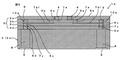
- FIG. 1 is a cross-sectional view of the multilayer wiring board 1. In FIG. 1, only the part related to the present invention is shown, and the other parts are not shown.
- the multilayer wiring board 1 is formed by laminating a ceramic laminate 2 in which a plurality of ceramic layers 2a are laminated and a plurality of resin insulating layers 3a to 3d. And a resin laminate 3 laminated on the body 2.
- a plurality of upper surface side connection electrodes 4 are formed on the upper surface of the uppermost resin insulation layer 3 a of the resin laminate 3 that is the upper surface of the multilayer wiring substrate 1.
- a plurality of lower surface side connection electrodes 5 provided corresponding to each upper surface side connection electrode 4 and connected to the corresponding upper surface side connection electrode 4 are provided on the lower surface of the ceramic laminate 2 which is the lower surface of the multilayer wiring board 1. It is formed.
- a plurality of upper surface side connection electrodes 4 are formed between the two upper surface side connection electrodes 4 in FIG. 1, and between the two lower surface side connection electrodes 5, an illustration is omitted.
- a plurality of lower surface side connection electrodes 5 are formed.
- the corresponding upper surface side connection electrode 4 and lower surface side connection electrode 5 are connected to the plurality of via conductors 6a to 6d, 8 and the plurality of in-plane conductors 7a to 7 formed inside the resin laminate 3 and the ceramic laminate. It is connected by an internal wiring composed of 7d.
- the pitch between the adjacent lower surface side connection electrodes 5 is set wider than the pitch between the adjacent upper surface side connection electrodes 4, and each of the corresponding upper surface side connection electrodes 4 and lower surface side connection electrodes 5 is connected to each other.
- a rewiring structure is formed in the ceramic laminate 2 and the resin laminate 3 by the internal wiring.
- a ceramic green sheet made of a low temperature co-fired ceramic (LTCC) mainly composed of a ceramic (for example, alumina) containing borosilicate glass is used. It can.
- LTCC low temperature co-fired ceramic
- HTCC high-temperature fired ceramic
- the ceramic laminate 2 may have a configuration in which a shrinkage suppression layer that suppresses shrinkage during firing of each ceramic layer 2a is disposed between adjacent ceramic layers 2a.
- a shrinkage suppression layer that suppresses shrinkage during firing of each ceramic layer 2a is disposed between adjacent ceramic layers 2a.
- a ceramic material that does not shrink at the firing temperature of each ceramic layer 2a can be used. If it does in this way, since the curvature of the ceramic laminated body 2 after baking will reduce, the curvature of the multilayer wiring board 1 will reduce in connection with this.
- Each lower surface side connection electrode 5 formed on the lower surface of the ceramic laminate 2 is formed by a printing technique using a conductive paste containing a metal such as Ag, Al, or Cu. At this time, Ni / Au plating may be further applied to the surface of each lower surface side connection electrode 5.
- the in-plane conductor 7d formed on the upper surface of the ceramic laminate 2 and the in-plane conductor (not shown) formed therein include a metal such as Ag, Al, or Cu on the main surface of each ceramic layer 2a. Each of them is formed by a printing technique using the contained conductive paste.
- the in-plane conductor 7d and the in-plane conductor (not shown) are formed of Ag.
- the via conductor 8 formed inside the ceramic laminate 2 in FIG. 1 is composed of a continuous body of via elements formed in each ceramic layer 2a, and each via element is, for example, a laser on the ceramic layer 2a.
- Each of the through-holes formed using, for example, is formed by filling a conductive paste containing any of Ag, Al, Cu, or the like using a printing technique.
- the resin insulation layers 3a to 3d forming the resin laminate 3 are each formed of a thermosetting resin such as polyimide or glass epoxy resin.
- the Young's modulus of each ceramic layer 2a is about 220 GPa, whereas each of the resin insulation layers 3a to 3d formed of polyimide is 1 to 5 GPa, and each of the resin insulation layers 3a to 3d Young's modulus is smaller than each ceramic layer 2a.
- the in-plane conductors 7a to 7c and the via conductors 6a to 6d formed in the resin laminate 3 Any of metals such as Cu, Ag, and Al can be used.
- the in-plane conductors 7a to 7c are respectively formed on the main surfaces of the predetermined resin insulating layers 3a to 3d.
- the ceramic laminate 2 is prepared in advance, and then the resin laminate 3 is laminated on the ceramic laminate 2.
- the resin laminate 3 on the ceramic laminate 2 is cured, a residual stress is generated in the laminated wiring board 1 due to curing shrinkage of the resin laminate 3, and the interface between the ceramic laminate 2 and the resin laminate 3 is generated. Peeling or warping of the laminated wiring board 1 occurs.
- Interfacial peeling between the ceramic laminate 2 and the resin laminate 3 occurs because of the adhesion strength at the interface between the adjacent ceramic layers 2a, the adhesion strength at the interfaces between the adjacent resin insulating layers 3a to 3d, and the adjacent ceramic layers 2a and the resin. This is because, among the adhesion strengths at the interface of the insulating layer 3d, the adhesion strength at the interface between the ceramic layer 2a made of a different material and the resin insulation layer 3d is the lowest. Further, at the interface between the ceramic layer 2a and the resin insulating layer 3d, the residual stress acts more strongly at the peripheral portion than at the central portion. Therefore, interface peeling between the ceramic laminate 2 and the resin laminate 3 often occurs with the peripheral edge of the interface as a base point.
- a plurality of dummy electrode pads that are not related to the wiring in the multilayer wiring board 1 are formed in the non-formation regions of the in-plane conductors 7a to 7c and the via conductors 6a to 6d in the resin multilayer body 3, respectively.
- 9 (corresponding to the “dummy conductor” of the present invention) is provided as an electrode for reducing the shrinkage stress when the resin laminate 3 is cured.
- the dummy electrode pads 9 are respectively disposed on the peripheral edge of the resin laminate 3 in plan view, which is a region where the residual stress is high in the resin laminate 3.
- positioning location of each above-mentioned dummy electrode pad 9 is an example, and if it is an empty space in the resin laminated body 3, it can change suitably. Further, the number of arrangements can be changed as appropriate.
- the inspection apparatus includes the above-described laminated wiring board 1 and a plurality of probe pins connected to the upper surface side connection electrodes 4 formed on the upper surface of the laminated wiring board 1, for example, a semiconductor element before dicing
- a probe card used in a wafer test such as (for example, LSI).
- this probe card determines the quality of the electrical characteristics of the LSI chip by applying the tip of the probe pin on the bonding pad of the LSI chip.
- the ceramic laminate 2 is prepared.
- the ceramic laminate 2 is formed by laminating the ceramic layers 2a prepared individually in a predetermined order, and pressing and firing the laminated layers.
- each via element body of the via conductor 8 formed in each ceramic layer 2a is formed, for example, by forming a via hole in the ceramic layer 2a by laser processing, and using Cu, Ag, Al of the via hole using a printing technique.
- Each is formed by filling a conductive paste containing any metal.
- the other via conductors excluding the via body are formed in the same manner.
- the in-plane conductor 7d formed on the main surface of each ceramic layer 2a is formed by a printing technique using a conductive paste containing any one metal of Cu, Ag, and Al (Ag in this embodiment). be able to.
- the resin laminate 3 can be formed by a build-up method or thin film lamination.
- an in-plane conductor 7c and a via conductor 6d are formed by laminating a resin insulating layer 3d with a copper foil on the upper surface of the prepared ceramic laminate 2.
- glass epoxy resin, polyimide, or the like can be used as a material for forming the resin insulating layer 3d.
- the in-plane conductor 7c can be obtained by patterning a copper foil by etching.
- the via conductor 6d is formed, for example, by forming a via hole in the resin insulating layer 3d by laser processing and performing via fill plating with a metal such as Cu, Ag, or Al on the via hole.
- the laminated wiring board 1 is obtained by repeating the lamination, via conductor formation, and in-plane conductor formation of the resin insulating layers 3a to 3c with copper foil for each layer.
- the dummy electrode pad 9 is also formed together with the in-plane conductor 7a.
- each upper surface side connection electrode 4 can be formed by the same method as each of the in-plane conductors 7a to 7c.
- the resin insulating layer 3d is formed on the prepared ceramic laminate 2 by applying polyimide or the like.
- an in-plane conductor 7c is formed after the via conductor 6d is formed by photolithography.
- a Ti film as a base electrode is formed on the resin insulating layer 3d by sputtering or the like, and a Cu film is formed on the Ti film by sputtering or the like. And it can form by forming a Cu film
- the multilayer wiring board 1 is obtained by repeatedly applying polyimide, forming via conductors, and forming in-plane conductors for the resin insulating layers 3a to 3c for each layer.
- the dummy electrode pad 9 is also formed together with the in-plane conductor 7a.
- Each upper surface side connection electrode 4 can be formed by a method similar to that for each of the in-plane conductors 7a to 7c.
- a Ni / Au film may be formed on each upper surface side connection electrode 4 and each lower surface side connection electrode 5 by electrolysis or electroless plating.
- the upper surface side connection electrodes 4 and the in-plane conductors 7a to 7c are surfaces formed on the ceramic laminate 2 by using a printing technique.
- the inner conductor for example, the in-plane conductor 7d
- the dummy electrode pad 9 for reducing the shrinkage stress of the resin laminate 3 is provided in the resin laminate 3, the resin laminate 3 is formed on the ceramic laminate 2. At this time, the dummy electrode pad 9 functions to suppress the contraction of the resin laminate 3. If it does so, since the stress which acts on the interface of the ceramic laminated body 2 and the resin laminated body 3 reduces, the interface peeling of the resin laminated body 3 and the ceramic laminated body 2 can be reduced.
- the stress acting on the interface between the ceramic laminate 2 and the resin laminate 3 is reduced, the warp of the multilayer wiring board 1 is reduced. Further, since the flatness of the in-plane conductors 7a to 7c formed in the resin laminate 1 is improved by reducing the warpage of the multilayer wiring board 1, the in-plane conductors 7a to 7c are curved. The increase in resistance value can be reduced.
- the residual stress generated by the curing shrinkage of the resin laminate 3 is higher at the peripheral portion than at the central portion at the interface between the ceramic laminate 2 and the resin laminate 3, and at this interface. Separation often occurs with the periphery of the interface as a base point. Accordingly, the dummy electrode pad 9 is arranged at the peripheral edge of the resin laminate 3 in a plan view, that is, by being arranged at a position close to the base point of the interface peeling between the semi-rack laminate 2 and the resin laminate 3, it acts on the base point. Since stress can be relaxed efficiently, reduction of interface peeling between the resin laminate 3 and the ceramic laminate 2 and reduction of warpage of the multilayer wiring board 1 are facilitated.
- each ceramic layer 2a is formed of a low-temperature co-fired ceramic (ceramic green sheet) whose main component is a ceramic containing borosilicate glass, and therefore, an in-plane conductor formed in the ceramic laminate 2 A low-resistance conductor such as Ag can be used for the wiring electrodes.
- the ceramic laminate 2 and the resin laminate 3 are arranged so that the pitch between the adjacent lower surface side connection electrodes 5 is wider than the pitch of the adjacent upper surface side connection electrodes 4.
- a rewiring structure is formed in the inside.
- the upper surface side connection electrodes 4 arranged at a narrow pitch are formed on the resin laminate 3 side where fine wiring can be easily formed.
- the multilayer wiring board 1 is suitable as a board used for a probe card for performing an electrical inspection of a recent semiconductor element in which terminals have a narrow pitch.
- FIG. 2 is a cross-sectional view of the laminated wiring board 1a. In FIG. 2, only the portion related to the present invention is shown, and the other portions are not shown.
- the laminated wiring board 1a according to this embodiment differs from the laminated wiring board 1 of the first embodiment described with reference to FIG. 1 in that the shrinkage provided in the resin laminate 3 is shown in FIG. That is, the plurality of dummy conductors for stress relaxation are composed of dummy electrode pads 9 and dummy via conductors 10a. Since other configurations are the same as those of the multilayer wiring board 1 of the first embodiment, the description thereof is omitted by giving the same reference numerals.
- a dummy via conductor 10a is provided in the resin insulating layer 3b at a position overlapping with the dummy electrode pad 9 in a plan view, and the upper end surface of the dummy via conductor 10a is connected to the dummy electrode pad 9.
- the dummy electrode pad 9 improves the fixing force of the dummy via conductor 10a to the resin laminate 3, so that the dummy via conductor 10a is connected to the dummy electrode pad. Compared with the case where there is not, the contraction stress relaxation effect of the resin laminated body 3 by the dummy via conductor 10a improves.
- the dummy conductor does not necessarily need to be configured by the dummy electrode pad 9 and the dummy via conductor 10a, and may be configured by only the dummy via conductor 10a.
- the lower end surface of the dummy via conductor 10a may be connected to another electrode pad. In this case, the adhering force of the dummy via conductor 10a to the resin laminate 3 is increased.
- FIG. 3 is a cross-sectional view of the multilayer wiring board 1b. In FIG. 3, only the part related to the present invention is shown, and the other parts are not shown.
- the laminated wiring board 1b according to this embodiment differs from the laminated wiring board 1a of the second embodiment described with reference to FIG. 2 in that it is formed on the upper surface of the resin insulating layer 3c as shown in FIG.
- the in-plane conductor 7b1 extends toward the dummy via conductor 10a, and the lower end surface of the dummy via conductor 10a is connected to the in-plane conductor 7b1. Since other configurations are the same as those of the multilayer wiring board 1a of the second embodiment, the description thereof is omitted by giving the same reference numerals.
- the adhesion force of the dummy via conductor 10a to the resin laminate 3 is improved by the in-plane conductor 7b1, so the dummy via conductor 10a becomes the in-plane conductor 7b1.
- the relaxation effect of the shrinkage stress of the resin laminate 3 by the dummy via conductor 10a is improved.
- FIG. 4 is a cross-sectional view of the multilayer wiring board 1c. In FIG. 4, only the parts related to the present invention are shown, and the other parts are not shown.
- the laminated wiring board 1c according to this embodiment differs from the laminated wiring board 1b of the third embodiment described with reference to FIG. 3 in that the resin insulation of the lowermost layer of the resin laminate 3 is shown in FIG.
- the via conductor 6d formed in the layer 3d and the end faces of the via conductor 8 formed in the ceramic laminate 2 are connected to each other, and the dummy conductor arrangement portion constituted by the dummy electrode pad 9 and the dummy via conductor 10a Is different. Since other configurations are the same as those of the multilayer wiring board 1b of the third embodiment, the description thereof is omitted by giving the same reference numerals.
- the via conductor 6d formed in the lowermost resin insulation layer 3d of the resin laminate 3 and the via conductor 6c formed in the resin insulation layer 3c on the via conductor 6d are formed in the ceramic laminate 2.
- the via conductors 8 are arranged at positions where they overlap with each other in plan view, and the end surfaces of the via conductor 8 of the ceramic laminate 2 and the via conductor 6d of the lowermost resin insulating layer 3d are connected to each other.
- the via conductor 6c of the resin insulating layer 3c and the via conductor 6d of the resin insulating layer 3d are connected via the in-plane conductor 7c.
- a dummy conductor composed of the dummy electrode pad 9 and the dummy via conductor 10a is connected to the in-plane conductor 7b1 formed on the upper surface of the resin insulating layer 3c, which connects the via conductor 6c and the via conductor 6b in the resin laminate 3. Is connected.
- the via conductor 8 formed in the ceramic laminate 2 in this embodiment corresponds to the “first via conductor” of the present invention, and the via conductor 6 d in the resin laminate 3 connected to the upper end surface of the via conductor 8.
- the via conductor 8 of the ceramic laminate 2 may be referred to as a first via conductor 8
- the via conductor 6d of the resin laminate 3 may be referred to as a second via conductor 6d.
- veer conductor 8 of the ceramic laminated body 2 and resin laminated body which are higher than the adhesive strength of the resin laminated body 3 and the ceramic laminated body 2 in the interface of the resin laminated body 3 and the ceramic laminated body 2 Since the connection portion of the third second via conductor 6d is formed, the adhesion strength at the interface between the resin laminate 3 and the ceramic laminate 2 is reinforced by the connection portion. Further, the first via conductor 8 and the second via conductor 6d are firmly connected, so that the second via conductor 6d in the resin laminate 3 functions as a support that prevents the resin laminate 2 from contracting. Therefore, interface peeling between the resin laminate 3 and the ceramic laminate 2 can be reduced.
- connection part of the 1st via conductor 8 and the 2nd via conductor 6d is arrange
- the resin laminated body to which the shrinkage stress of the resin laminated body 3 acts strongly 3 and the peripheral portion of the interface between the ceramic laminate 2 are reinforced by the connection portion between the first via conductor 8 and the second via conductor 6d. Therefore, interface peeling between the resin laminate 3 and the ceramic laminate 2 can be reduced by the connection portion.
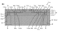
- FIGS. 5 is a cross-sectional view of the multilayer wiring board 1d
- FIG. 6 is a plan view of the multilayer wiring board 1d. In FIGS. 5 and 6, only the portion related to the present invention is shown, and the other portions are not shown.
- the laminated wiring board 1d according to this embodiment differs from the laminated wiring board 1c of the fourth embodiment described with reference to FIG. 4 in that the first via conductor 8 of the ceramic laminated body 2 is shown in FIG. A second via conductor 6d of the resin laminate 3, a via conductor 6c formed in the resin insulating layer 3c on the resin insulating layer 3d on which the second via conductor 6d is formed, and a dummy via conductor 10a. In other words, they are arranged at positions where they are superposed in plan view.
- Other configurations are the same as those of the laminated wiring board 1c of the fourth embodiment, and therefore, the description thereof is omitted by giving the same reference numerals.
- the dummy via conductor 10a is connected to the first via conductor 6b via the in-plane conductor 7b1, via conductor 6c, and in-plane conductor 7c disposed between the dummy via conductor 10a and the second via conductor 6d. It is connected to the end face (upper end face) opposite to the end face (lower end face) connected to the via conductor 8.
- the resin laminate 3 has a rectangular shape in plan view, and dummy via conductors 10a are disposed at the four corners of the rectangular resin laminate 3, respectively.
- Such an arrangement configuration of the dummy via conductors 10a can be said to be that the pair of dummy via conductors 10a arranged on the same diagonal line are arranged at point-symmetrical positions with respect to the center of the resin laminate 3 in plan view.
- FIG. 6 shows a plurality of other via conductors 11 formed inside the ceramic laminate 2 (not shown in FIG. 5).
- the other via conductors 11 and the first via conductors 8 are Each is connected to the corresponding lower surface side connection electrode 5.
- the dummy via conductor 10a is disposed at a position where it overlaps with each of the first via conductor 8 and the second via conductor 6d in plan view, and is connected to the first via conductor 8 at the end faces.
- the two via conductors 6d are connected via the via conductors 6c and the like.
- the resin laminate 3 tends to shrink from the periphery toward the center when viewed in a plan view, for example.
- the dummy via conductor 10a is disposed only in one of the four corners of the resin laminate 3 in a plan view, around the place where the dummy via conductor 10a is disposed in the resin laminate 3. While the shrinkage stress relaxation amount is large, the shrinkage stress relaxation amount around the remaining corners is small. As a result, an unbalance of the amount of relaxation of the shrinkage stress occurs in the resin laminate 3 and the warp of the laminated wiring board 1 may occur.
- the pair of dummy via conductors 10a positioned on the same diagonal line of the resin laminate 3 having a rectangular shape in plan view can be It will be arranged at a point-symmetrical position with respect to the center. Then, since the balance of the shrinkage suppression amount by each dummy via conductor 10a is improved in the resin laminate 3, the warp of the laminated wiring board 1d can be reduced.
- the shrinkage stress acts most strongly at the four corners when the resin laminate 3 contracts, and therefore the resin laminate 3 and the ceramic laminate 2.
- the interfacial peeling is likely to occur with the four corners as base points. Therefore, by disposing the dummy via conductors 10a at the four corners of the resin laminate 3, the shrinkage stress acting on the four corners is reduced, so that the interface peeling between the resin laminate 3 and the ceramic laminate 2 can be reduced. .
- FIG. 7 is a view showing a modification of the arrangement configuration of the dummy via conductors 10a, and corresponds to FIG.
- the dummy via conductors 10a are arranged only at the four corners of the rectangular resin laminate 3 in plan view.
- the dummy via conductors 10a may be arranged side by side at predetermined intervals along each side. In this way, since the dummy via conductors 10a can relieve the shrinkage stress at the time of curing shrinkage in substantially the entire region of the peripheral edge that is the base point of the interface peeling between the resin laminate 3 and the ceramic laminate 2, The effect of reducing interfacial peeling is further improved.
- the dummy via conductors 10a are arranged in a balanced manner (point-symmetric arrangement) at the peripheral edge of the resin laminate 3, it is possible to reduce the warpage of the laminated wiring board 1d.
- FIG. 8 is a cross-sectional view of the multilayer wiring board 1e. Moreover, in FIG. 8, only the part relevant to this invention is shown in figure, and the other part is abbreviate
- the laminated wiring board 1e according to this embodiment differs from the laminated wiring board 1d of the fifth embodiment described with reference to FIG. 5 in that the first via conductor 8 of the ceramic laminated body 2 is shown in FIG.
- another dummy via conductor 10b different from the dummy via conductor 10a arranged at a position overlapping in plan view is further provided. Since other configurations are the same as those of the multilayer wiring board 1d of the fifth embodiment, the description thereof is omitted by attaching the same reference numerals.
- another dummy via conductor 10b is further connected to the in-plane conductor 7b1 to which the lower end surface of the dummy via conductor 10a is connected.
- one dummy via conductor 10b is provided above and below the in-plane conductor 7b1, and both dummy via conductors 10b are arranged at positions where they overlap in plan view.
- both dummy via conductors 10b are connected to the dummy electrode pad 9b at the end surface opposite to the end surface connected to the in-plane conductor 7b1, and the dummy conductors are respectively constituted by the dummy via conductor 10b and the dummy electrode pad 9b.
- FIG. 9 is a cross-sectional view of the laminated wiring board 1f. In FIG. 9, only the part related to the present invention is shown, and the other parts are not shown.
- the laminated wiring board 1f according to this embodiment differs from the laminated wiring board 1d of the fifth embodiment described with reference to FIG. 5 in that, as shown in FIG. 9, the volume of the dummy via conductor 10a is a resin laminated body. 3 is larger than the via conductors 6a to 6d formed in the circuit board. Since other configurations are the same as those of the multilayer wiring board 1d of the fifth embodiment, the description thereof is omitted by giving the same reference numerals.
- the effect of reducing the shrinkage stress of the resin laminate 3 by the dummy via conductor 10a is improved. Therefore, the in-plane conductors 7a, 7b1, and 7b1 in the resin laminate 3 are caused by the peeling of the interface between the resin laminate 3 and the ceramic laminate 2, the warpage of the laminated wiring board 1f, and the flatness of the resin laminate 3. Each increase in the resistance value of 7c can be reduced.
- FIG. 10 is a cross-sectional view of the laminated wiring board 1g. In FIG. 10, only the parts related to the present invention are shown, and the other parts are not shown.
- the laminated wiring board 1g according to this embodiment is different from the laminated wiring board 1d of the fifth embodiment described with reference to FIG. 5 in that the area in plan view of the resin laminate 3 is as shown in FIG. It is smaller than the ceramic laminate 2. Since other configurations are the same as those of the multilayer wiring board 1d of the fifth embodiment, the description thereof is omitted by attaching the same reference numerals.
- the shrinkage stress acting on the peripheral edge of the interface which is the base point of the interface peeling between the resin laminate 3 and the semi-rack laminate 2 increases as the area of the resin laminate 3 in plan view increases. Get higher. Therefore, by making the area of the resin laminate 3 in plan view smaller than that of the ceramic laminate 2, the resin laminate 3 and the ceramic laminate 2 can be made to have the same area in plan view. Interfacial peeling between the laminate 3 and the ceramic laminate 2 can be reduced.
- FIG. 11 is a cross-sectional view of the laminated wiring board 1h. Moreover, in FIG. 11, only the part relevant to this invention is shown in figure, and the other part is abbreviate
- the laminated wiring board 1h according to this embodiment differs from the laminated wiring board 1d of the fifth embodiment described with reference to FIG. 5 in that the second via conductor 6d of the resin laminate 3 is shown in FIG.
- the lower end surface of the via conductor 8a (corresponding to the “first via conductor” of the present invention, hereinafter referred to as the first via conductor 8a) of the ceramic laminate 2 connected at the end surfaces to each other is ceramic. It is connected to the electrode pad 12 provided in the laminated body 2. Since other configurations are the same as those of the multilayer wiring board 1d of the fifth embodiment, the description thereof is omitted by giving the same reference numerals.
- the first via conductor 8 of the fifth embodiment shown in FIG. 5 is formed through the ceramic laminate 2, but in this embodiment, the length of the first via conductor 8a is short,
- the electrode pad 12 is connected to the lower end surface which is the end surface opposite to the end surface connected to the second via conductor 6d of the first via conductor 8a. Further, the electrode pad 12 and the lower surface side connection electrode 5 are arranged between the electrode pad 12 and the lower surface side connection electrode 5 by another via conductor 8b disposed at a position overlapping with the first via conductor 8a in plan view. Is connected.
- the electrode pad 12 improves the adhesion of the first via conductors 8a and 8b to the ceramic laminate 2, so that the first via conductor 8 penetrates the ceramic laminate 2 as shown in FIG. Compared with the case where it was formed, the curvature of the ceramic laminated body 2 can be reduced more.
- each multilayer wiring board 1, 1 a to 1 h is configured by the ceramic laminate 2 and the resin laminate 3 laminated on the upper surface of the ceramic laminate 2.
- the resin laminate 3 may be arranged on both the upper and lower surfaces of the ceramic laminate 2. In this way, the shrinkage stress of the resin laminate 3 on the upper surface side of the ceramic laminate 2 is offset by the shrinkage stress of the resin laminate 3 on the lower surface side, so that the warpage of the multilayer wiring board can be reduced.
- a laminated wiring board may be formed by combining the configurations of the above-described embodiments.
- the present invention can be applied to various laminated wiring boards in which a resin laminate is laminated on a ceramic laminate.
Abstract
セラミック積層体上に樹脂積層体が積層されて成る積層配線基板において、樹脂積層体とセラミック積層体の界面剥離を低減させるとともに、積層配線基板の反りを低減させる。 積層配線基板1は、複数のセラミック層2aが積層されて成るセラミック積層体2と、複数の樹脂絶縁層3a~3dが積層されて成り、セミラック積層体2に積層された樹脂積層体3とを備え、樹脂積層体3内に、該樹脂積層体の収縮応力緩和用のダミー電極パッド9が設けられている。このようにすると、ダミー電極パッド9が樹脂積層体3の収縮に対し収縮抑制の働きをすることになるため、セラミック積層体2と樹脂積層体3との界面に作用する応力が減少し、これにより、樹脂積層体3とセラミック積層体2の界面剥離並びに積層配線基板1の反りを低減することができる。
Description
本発明は、セラミック層と樹脂絶縁層とで構成された積層配線基板およびこの積層配線基板を備える検査装置に関する。
LSIなどの半導体素子の電気検査には、セラミック多層基板上にプローブピンを形成したプローブカードが広く採用されている。また、近年では、半導体素子の高集積化により、その端子数の増加や、端子の狭ピッチ化が進んでいるため、セラミック多層基板の一部の層を、微細な配線形成が容易なポリイミドなどの樹脂絶縁層に置き換えた積層配線基板が用いられるようになっている。
例えば、特許文献1に記載の積層配線基板100では、図12に示すように、複数のセラミック層101aが積層されて成るセラミック積層体101と、複数の樹脂絶縁層102aが積層されて成る樹脂積層体102とを備え、セラミック積層体101上に樹脂積層体102が積層された構造となっている。このとき、積層配線基板100の上面には、それぞれプローブピンに接続される複数の表面電極103が狭ピッチで形成される。また、積層配線基板100の下面には、各表面電極103に対応して設けられ、対応する表面電極103にそれぞれ接続された複数の裏面電極104が形成される。各裏面電極104は、外部の実装基板との接続用に設けられている。
また、樹脂積層体102およびセラミック積層体101の内部には、隣接する裏面電極104間のピッチが、隣接する表面電極103間のピッチよりも広くなるように、再配線構造が形成されている。
このような再配線構造を形成するに当たり、表面電極103に近い方の樹脂積層体102では、その内部に形成する配線の細線化や、隣接する配線間の距離を狭くする必要があるため、微細な配線形成が可能なポリイミド等から成る樹脂絶縁層102aで構成されている。また、比較的配線の形成スペースに余裕があるセラミック積層体101では、樹脂絶縁層102aよりも剛性が高く、線膨張係数がICウエハ等の検査媒体の線膨張係数に近いセラミック層101aで構成されている。積層配線基板100をこのように構成することで、端子数の増加や、端子間が狭ピッチ化された近年の半導体素子の電気検査を可能にしている。
しかしながら、従来の積層配線基板100は、セラミック積層体101と樹脂積層体102の積層構造で形成されているため、例えば、セラミック積層体101上に樹脂積層体102を形成する際、樹脂積層体102の硬化収縮により、積層配線基板100の内部に残留応力が発生する。
積層配線基板100の内部に残留応力が発生すると、セラミック積層体101と樹脂積層体102との界面で剥離が生じたり、積層配線基板100の反りが生じるおそれがある。
本発明は、上記した課題に鑑みてなされたものであり、セラミック積層体上に樹脂積層体が積層されて成る積層配線基板において、樹脂積層体とセラミック積層体の界面剥離を低減させるとともに、積層配線基板の反りを低減させることを目的とする。
上記した目的を達成するために、本発明の積層配線基板は、複数のセラミック層が積層されて成るセラミック積層体と、複数の樹脂絶縁層が積層されて成り、前記セラミック積層体に積層された樹脂積層体とを備え、前記樹脂積層体内に、前記樹脂積層体の収縮応力緩和用のダミー導体が設けられていることを特徴としている。
この場合、樹脂積層体内に、該樹脂積層体の収縮応力緩和用のダミー導体が設けられるため、セラミック積層体上に樹脂積層体を形成する際、ダミー導体が樹脂積層体の収縮に対し収縮抑制の働きをすることになる。そうすると、セラミック積層体と樹脂積層体との界面に作用する応力が減少するため、樹脂積層体とセラミック積層体の界面剥離を低減することができる。
また、セラミック積層体と樹脂積層体との界面に作用する応力が減少することで、積層配線基板の反りが低減する。
また、前記ダミー導体は、平面視で前記樹脂積層体の周縁部に配置されているのが好ましい。セラミック積層体と樹脂積層体の界面において、樹脂積層体の収縮により生じる応力は、その中央部よりも周縁部の方が高く、この界面での剥離は、該界面の周縁を基点として生じる場合が多い。そこで、ダミー導体を平面視で樹脂積層体の周縁部に配置、すなわち、セミラック積層体と樹脂積層体の界面剥離の基点に近い位置に配置する。このようにすると、基点に作用する応力を効率的に緩和させることができるため、樹脂積層体とセラミック積層体の界面剥離の低減および積層配線基板の反りの低減が容易なものとなる。
また、前記ダミー導体は、ダミービア導体であってもかまわない。ダミー導体は、その体積が大きいほど、セミラック積層体と樹脂積層体の界面剥離、および、積層配線基板の反り低減効果が高い。したがって、ダミー導体をダミービア導体とすることで、例えば、ダミー導体を面内導体により形成する場合と比較して、容易にその体積を大きくすることができるため、前記界面剥離、および、積層配線基板の反りの低減を容易に実現することができる。
また、前記ダミービア導体を複数備え、前記複数のダミー導体のうち、少なくとも一対の前記ダミー導体が、平面視で前記樹脂積層体の中心に対して点対称の位置に配置されていてもよい。樹脂積層体が硬化収縮する場合、該樹脂積層体は、例えば平面視した場合に、その周縁から中心に向けて縮まろうとする。ここで、樹脂積層体を平面視したときに、各ダミー導体を樹脂積層体の中心に対して偏った位置に配置すると、樹脂積層体の各ダミービア導体が配置された部分の収縮抑制量が、前記中心を基準として樹脂積層体の各ダミービア導体の配置箇所と逆側の部分の収縮抑制量よりも多くなる。そうすると、樹脂積層体内で収縮抑制量のアンバランスが生じて積層配線基板の反りが生じる。そこで、少なくとも一対のダミービア導体を、平面視で樹脂積層体の中心に対して点対称の位置に配置することで、樹脂積層体の前記一対のダミービア導体が配置された箇所において、収縮抑制量のバランスがよくなるため、積層配線基板の反りを低減することができる。
また、前記樹脂積層体は、平面視で矩形状を有し、平面視において、前記樹脂積層体の四隅部それぞれに前記ダミービア導体が配置されていてもよい。樹脂積層体が、平面視で矩形状を有する場合、樹脂積層体の収縮時に、その収縮応力が最も強く作用するのが四隅部であるため、樹脂積層体とセラミック積層体の界面剥離は当該四隅部を基点として生じ易い。そこで、樹脂積層体の四隅部それぞれにダミービア導体を配置することで、四隅部に作用する収縮応力を緩和することができるため、樹脂積層体のセラミック積層体からの剥離を低減することができる。また、各ダミービア導体は、平面視で樹脂積層体の中心に対して点対称の位置に配置されることになるため、積層配線基板の反りを低減することもできる。
また、前記樹脂積層体内に形成された面内導体をさらに備え、前記ダミービア導体が、前記面内導体に接続されていてもよい。このようにすると、面内導体により、ダミービア導体の樹脂積層体への固着力が向上するため、ダミービア導体が面内導体に接続されていない場合と比較して、ダミービア導体による樹脂積層体の収縮応力の緩和効果が向上する。
また、前記ダミービア導体と異なる他のダミービア導体をさらに備え、前記面内導体に、前記他のダミービア導体が接続されていてもよい。この場合、面内導体に、樹脂積層体の収縮応力緩和用のダミー導体が複数接続されることになるため、樹脂積層体の収縮応力の緩和効果がさらに向上する。
また、前記セラミック積層体内に設けられた第1ビア導体と、前記樹脂積層体内に設けられた第2ビア導体とをさらに備え、前記第1ビア導体と第2ビア導体の端面同士が接続されていてもよい。この場合、樹脂積層体とセラミック積層体の界面に、樹脂積層体とセラミック積層体との密着強度よりも高い、第1ビア導体と第2ビア導体の接続部が形成されるため、樹脂積層体とセラミック積層体の界面の密着強度が当該接続部により補強される。また、第1ビア導体と第2ビア導体が強固に接続されることで、樹脂積層体内の第2ビア導体が、樹脂積層体の収縮を妨げる支持体のように機能するため、樹脂積層体とセラミック積層体の界面剥離を低減することができる。
また、前記第1ビア導体と前記第2ビア導体との接続部が、平面視で前記樹脂積層体の周縁部に配置されていてもよい。この場合、樹脂積層体の収縮応力が強く作用する、樹脂積層体とセラミック積層体の界面の周縁部が、第1ビア導体と第2ビア導体との接続部により補強されるため、樹脂積層体とセラミック積層体の界面剥離をさらに低減することができる。
また、所定の前記ダミービア導体が、前記第2ビア導体の前記第1ビア導体に接続された端面と反対側の端面に接続されることにより、前記第1ビア導体、前記第2ビア導体および前記所定のダミー導体が平面視で重なる位置にそれぞれ配置されていてもよい。このようにすると、樹脂積層体の収縮応力緩和用のダミービア導体が、セラミック積層体内に形成された第1ビア導体に支持されることになるため、ダミービア導体を、第2ビア導体とともに、樹脂積層体の収縮を妨げる支持体として機能させることができる。
また、前記第1ビア導体の前記第2ビア導体に接続される端面と反対側の端面が、前記セラミック積層体内に設けられた電極パッドに接続されていてもよい。このようにすると、電極パッドによりセラミック積層体の反りを低減させることができるため、積層配線基板の反りを低減することができる。
前記ダミー導体の体積が、前記第2ビア導体の体積よりも大きくてもかまわない。このようにすると、ダミービア導体の体積を第2ビア導体と同じに形成する場合と比較して、ダミービア導体による樹脂積層体の収縮応力緩和効果が向上するため、樹脂積層体とセラミック積層体の界面剥離、積層配線基板の反り、および、樹脂積層体の平坦度が悪くなることに起因する面内導体の抵抗値の増大を、それぞれ低減することができる。
前記樹脂積層体の平面視での面積が、前記セラミック積層体の平面視での面積よりも小さくてもかまわない。樹脂積層体の収縮時において、樹脂積層体とセミラック積層体の界面剥離の基点となる該界面の周縁部に作用する収縮応力は、樹脂積層体の平面視での面積が大きいほど高くなる。したがって、樹脂積層体の平面視での面積をセラミック積層体よりも小さくすることで、両積層体の平面視での面積を等しく形成する場合と比較して、樹脂積層体とセラミック積層体の界面剥離を低減することができる。
また、前記ダミービア導体の両端面のうちの少なくとも一方が、前記樹脂積層体内に設けられた電極パッドに接続されていてもよい。このようにすると、電極パッドにより、ダミービア導体の樹脂積層体への固着力が向上するため、ダミービア導体が電極パッドに接続されていない場合と比較して、ダミービア導体による樹脂積層体の収縮応力の緩和効果が向上する。
また、前記複数のセラミック層それぞれは、ホウケイ酸系ガラスを含有するセラミックを主成分とするセラミックグリーンシートで形成されていてもよい。この場合、セラミック積層体を形成するセラミック層として、低温同時焼成セラミック(LTCC)を用いることができる。また、セラミック積層体内に形成する面内導体等の配線電極に低抵抗導体のAg等を使用することができる。
また、前記セラミック積層体は、前記セラミック層の焼成時の収縮を抑制する収縮抑制層をさらに備えていてもよい。この場合、セラミック積層体の反りが低減するため、これに伴って積層配線基板の反りも低減することができる。
また、前記樹脂積層体の上面に形成された複数の上面側接続電極と、前記複数の上面側接続電極に対応して設けられ、対応する前記上面側接続電極にそれぞれ接続された複数の下面側接続電極とをさらに備え、隣接する前記下面側接続電極間のピッチが、隣接する前記上面側接続電極間のピッチよりも広くなるように、前記セラミック積層体および前記樹脂積層体内の配線構造が形成されていてもよい。この場合、その内部に再配線構造が形成された積層配線基板において、樹脂積層体とセラミック積層体の界面剥離、積層配線基板の反り、および、樹脂積層体の反りに起因する樹脂積層体内の配線の抵抗値の増大それぞれを低減することができる。
また、この積層配線基板を、半導体を検査する検査装置に用いてもよい。この場合、各上面側接続電極それぞれに、例えばプローブピンを接続させることで、積層配線基板をプローブカードとして使用することができる。
本発明によれば、樹脂積層体内に、該樹脂積層体の収縮応力緩和用のダミー導体が設けられるため、セラミック積層体上に樹脂積層体を形成する際、ダミー導体が樹脂積層体の収縮に対し収縮抑制の働きをすることになる。そうすると、セラミック積層体と樹脂積層体との界面に作用する応力が減少するため、樹脂積層体とセラミック積層体の界面剥離を低減することができる。
また、セラミック積層体と樹脂積層体との界面に作用する応力が減少することで、積層配線基板の反りが低減する。
<第1実施形態>
本発明の第1実施形態にかかる積層配線基板1について、図1を参照して説明する。なお、図1は積層配線基板1の断面図である。また、図1では、本発明に関係する部分のみを図示し、その他の部分は図示省略している。
本発明の第1実施形態にかかる積層配線基板1について、図1を参照して説明する。なお、図1は積層配線基板1の断面図である。また、図1では、本発明に関係する部分のみを図示し、その他の部分は図示省略している。
この実施形態にかかる積層配線基板1は、図1に示すように、複数のセラミック層2aが積層されて成るセラミック積層体2と、複数の樹脂絶縁層3a~3dが積層されて成り、セラミック積層体2に積層された樹脂積層体3とを備えている。また、積層配線基板1の上面となる樹脂積層体3の最上層の樹脂絶縁層3aの上面には、複数の上面側接続電極4が形成される。積層配線基板1の下面となるセラミック積層体2の下面には、各上面側接続電極4に対応して設けられ、対応する上面側接続電極4にそれぞれ接続された複数の下面側接続電極5が形成される。
また、図1中の2つの上面側接続電極4の間には、それぞれ図示省略の複数の上面側接続電極4が形成されるとともに、2つの下面側接続電極5の間にも、図示省略の複数の下面側接続電極5が形成される。このとき、対応する上面側接続電極4および下面側接続電極5同士は、樹脂積層体3およびセラミック積層体の内部に形成された複数のビア導体6a~6d,8および複数の面内導体7a~7dとで構成された内部配線により接続されている。
また、隣接する下面側接続電極5間のピッチが、隣接する上面側接続電極4間のピッチよりも広く設定されており、対応する上面側接続電極4および下面側接続電極5同士を接続する各内部配線により、セラミック積層体2および樹脂積層体3内において再配線構造が形成されている。
セラミック積層体2を形成する各セラミック層2aには、それぞれ、ホウケイ酸系ガラスを含有するセラミック(例えば、アルミナ)を主成分とする低温同時焼成セラミック(LTCC)から成るセラミックグリーンシートを用いることができる。また、各セラミック層2aを形成するその他の材料としては、高温焼成セラミック(HTCC)等、種々のセラミック材料を用いることもできる。
なお、セラミック積層体2は、隣接するセラミック層2a間に、各セラミック層2aの焼成時の収縮を抑制する収縮抑制層を配置する構成であってもかまわない。この収縮抑制層には、各セラミック層2aの焼成温度では収縮しないセラミック材料を用いることができる。このようにすると、焼成後のセラミック積層体2の反りが低減するため、これに伴って、積層配線基板1の反りが低減する。
セラミック積層体2の下面に形成された各下面側接続電極5は、Ag、Al、Cu等の金属を含有する導電性ペーストを用いた印刷技術等によりそれぞれ形成される。このとき、各下面側接続電極5の表面に、Ni/Auめっきをさらに施すようにしてもよい。
また、セラミック積層体2上面に形成された面内導体7d、および、その内部に形成された図示省略の面内導体は、各セラミック層2aの主面に、Ag、Al、Cu等の金属を含有する導電性ペーストを用いた印刷技術等によりそれぞれ形成されている。なお、この実施形態では、面内導体7dおよび図示省略の面内導体が、Agによりそれぞれ形成される。
図1中のセラミック積層体2の内部に形成されたビア導体8は、各セラミック層2aそれぞれに形成されたビア素体の連続体から成り、各ビア素体は、例えば、セラミック層2aにレーザ等を用いて形成した貫通孔に、印刷技術を用いて、Ag、Al、Cu等のいずれかを含有する導電性ペーストを充填することによりそれぞれ形成される。
樹脂積層体3を形成する各樹脂絶縁層3a~3dは、それぞれ、ポリイミドやガラスエポキシ樹脂等の熱硬化性樹脂で形成される。このとき、各セラミック層2aのヤング率は約220GPaであるのに対して、例えば、ポリイミドで形成された各樹脂絶縁層3a~3dは、1~5GPaであり、各樹脂絶縁層3a~3dのヤング率が、各セラミック層2aよりも小さい。
また、樹脂積層体3の上面に形成される各上面側接続電極4、樹脂積層体3の内部に形成される各面内導体7a~7cおよび各ビア導体6a~6dそれぞれを形成する材料として、Cu、Ag、Al等の金属のいずれかを用いることができる。各面内導体7a~7cは、所定の樹脂絶縁層3a~3dの主面にそれぞれ形成されている。
以上のように構成された積層配線基板1では、セラミック積層体2が先に準備された後、このセラミック積層体2上に樹脂積層体3が積層されることにより製造される。ここで、セラミック積層体2上の樹脂積層体3を硬化させるときに、積層配線基板1内に樹脂積層体3の硬化収縮による残留応力が発生し、セラミック積層体2と樹脂積層体3の界面剥離や積層配線基板1の反り等が発生する。
セラミック積層体2と樹脂積層体3の界面剥離が発生するのは、隣接するセラミック層2aの界面の密着強度、隣接する樹脂絶縁層3a~3dの界面の密着強度および隣接するセラミック層2aと樹脂絶縁層3dの界面の密着強度のうち、異種材料で構成されたセラミック層2aと樹脂絶縁層3dの界面の密着強度が一番低いためである。また、セラミック層2aと樹脂絶縁層3dの界面においては、その中央部よりも周縁部の方が前記残留応力が強く作用する。したがって、セラミック積層体2と樹脂積層体3の界面剥離は、その界面の周縁部を基点として発生する場合が多い。
そこで、この実施形態では、樹脂積層体3内における、面内導体7a~7cやビア導体6a~6dの非形成領域に、それぞれ積層配線基板1内の配線とは関係のない複数のダミー電極パッド9(本発明の「ダミー導体」に相当)が、樹脂積層体3の硬化時の収縮応力緩和用の電極として設けられている。このダミー電極パッド9は、樹脂積層体3内で前記残留応力が高い領域である平面視で樹脂積層体3の周縁部にそれぞれ配置される。なお、上記した各ダミー電極パッド9の配置箇所は一例であり、樹脂積層体3内の空きスペースであれば、適宜、変更可能である。また、その配置数も、適宜変更可能である。
本発明に係る検査装置は、上記した積層配線基板1と、積層配線基板1の上面に形成された各上面側接続電極4に接続された複数のプローブピンとを備え、例えば、ダイシング前の半導体素子(例えば、LSI)などのウエハテストで使用されるプローブカードである。具体的には、このプローブカードは、LSIチップのボンディングパッド上にプローブピンの先端を当てることにより、LSIチップの電気的特性の良否を判別する。
次に、積層配線基板1の製造方法について説明する。なお、以下に説明する製造方法は、後述する他の実施形態にかかる積層配線基板1a~1hに適用することができる。
まず、セラミック積層体2を準備する。このとき、セラミック積層体2は、個別に準備された各セラミック層2aを所定の順序で積層し、この積層されたものを圧着・焼成して形成する。ここで、各セラミック層2aに形成されるビア導体8の各ビア素体は、例えば、レーザ加工によりセラミック層2aにビアホールを形成し、該ビアホールに印刷技術を用いて、Cu、Ag、Alのいずれかの金属を含有する導電性ペーストを充填することによりそれぞれ形成する。また、ビア素体を除くその他のビア導体も同様にして形成する。また、各セラミック層2aの主面に形成される面内導体7dは、Cu、Ag、Alのいずれかの金属(この実施形態ではAg)を含有する導電性ペーストを用いた印刷技術により形成することができる。
樹脂積層体3は、ビルドアップ工法または薄膜積層により形成することができる。ビルドアップ工法では、準備したセラミック積層体2の上面に、銅箔付の樹脂絶縁層3dを積層し、面内導体7cおよびビア導体6dを形成する。このとき、樹脂絶縁層3dを形成する材料として、ガラスエポキシ樹脂やポリイミド等を用いることができる。また、面内導体7cは銅箔をエッチングによりパターン形成することで得られる。ビア導体6dは、例えば、樹脂絶縁層3dにレーザ加工でビアホールを形成し、該ビアホールにCu、Ag、Alなどの金属をビアフィルめっきするなどして形成する。
その後は、同様に、1層ごとに、銅箔付の樹脂絶縁層3a~3cの積層・ビア導体形成・面内導体形成を繰り返すことにより、積層配線基板1を得る。このとき、樹脂絶縁層3bにおいては、面内導体7aとともにダミー電極パッド9も形成する。また、各上面側接続電極4は、各面内導体7a~7cと同様の方法によりそれぞれ形成することができる。
薄膜積層により樹脂積層体3を形成する場合は、準備したセラミック積層体2上に、ポリイミドを塗布するなどして樹脂絶縁層3dを形成する。樹脂絶縁層3dには、フォトリソグラフィ加工によりビア導体6dを形成した後、面内導体7cを形成する。面内導体7cは、例えば、樹脂絶縁層3d上に、下地電極としてのTi膜をスパッタ等により成膜し、同じくスパッタ等によりTi膜上にCu膜を成膜する。そして、Cu膜上に、電解または無電解めっきにより、同じくCu膜を成膜することで形成することができる。
その後は、同様に、1層ごとに、樹脂絶縁層3a~3cとなるポリイミドの塗布・ビア導体形成・面内導体形成を繰り返すことにより、積層配線基板1を得る。このとき、樹脂絶縁層3bにおいては、面内導体7aとともに、ダミー電極パッド9も形成する。また、各上面側接続電極4は、各面内導体7a~7cと同様の方法により形成することができる。
なお、各上面側接続電極4および各下面側接続電極5上に、電解または無電解めっきによりNi/Au膜を形成してもかまわない。
このように、ビルドアップ工法や薄膜積層により樹脂積層体3を形成した場合、各上面側接続電極4および各面内導体7a~7cは、セラミック積層体2に印刷技術を用いて形成される面内導体(例えば、面内導体7d)と比較して、微細なパターン形成が可能となる。
したがって、上記した実施形態によれば、樹脂積層体3内に、該樹脂積層体3の収縮応力緩和用のダミー電極パッド9が設けられるため、セラミック積層体2上に樹脂積層体3を形成する際、ダミー電極パッド9が樹脂積層体3の収縮に対し収縮抑制の働きをすることになる。そうすると、セラミック積層体2と樹脂積層体3との界面に作用する応力が減少するため、樹脂積層体3とセラミック積層体2の界面剥離を低減することができる。
また、セラミック積層体2と樹脂積層体3の界面に作用する応力が減少することで、積層配線基板1の反りが低減する。また、積層配線基板1の反りが低減することで、樹脂積層体1内に形成された面内導体7a~7cの平坦性が向上するため、面内導体7a~7cが湾曲することに起因した抵抗値の増大を低減することができる。
ところで、上記したように、樹脂積層体3の硬化収縮により生じる残留応力は、セラミック積層体2と樹脂積層体3との界面において、その中央部よりも周縁部の方が高く、この界面での剥離は、該界面の周縁を基点として生じる場合が多い。したがって、ダミー電極パッド9を平面視で樹脂積層体3の周縁部に配置、すなわち、セミラック積層体2と樹脂積層体3の界面剥離の基点に近い位置に配置することで、当該基点に作用する応力を効率的に緩和させることができるため、樹脂積層体3とセラミック積層体2の界面剥離の低減および積層配線基板1の反りの低減が容易なものとなる。
また、前記各セラミック層2aそれぞれは、ホウケイ酸系ガラスを含有するセラミックを主成分とする低温同時焼成セラミック(セラミックグリーンシート)で形成されているため、セラミック積層体2内に形成する面内導体等の配線電極に低抵抗導体のAg等を使用することができる。
また、この実施形態にかかる積層配線基板1は、隣接する下面側接続電極5間のピッチが、隣接する上面側接続電極4のピッチよりも広くなるように、セラミック積層体2および樹脂積層体3の内部に再配線構造が形成されている。ここで、狭いピッチで配置された各上面側接続電極4が、微細な配線形成が容易な樹脂積層体3側に形成されている。
また、積層配線基板1をセラミック積層体2と樹脂積層体3とで構成した場合の弊害である、セラミック積層体2と樹脂積層体3の界面剥離や積層配線基板1の反りは、樹脂積層体3内に設けられたダミー電極パッド9により低減される。そのため、積層配線基板1は、端子の狭ピッチ化が進んでいる近年の半導体素子の電気的検査を行うためのプローブカードに用いられる基板として好適である。
<第2実施形態>
本発明の第2実施形態にかかる積層配線基板1aについて、図2を参照して説明する。なお、図2は積層配線基板1aの断面図である。また、図2では、本発明に関係する部分のみを図示し、その他の部分は図示省略している。
本発明の第2実施形態にかかる積層配線基板1aについて、図2を参照して説明する。なお、図2は積層配線基板1aの断面図である。また、図2では、本発明に関係する部分のみを図示し、その他の部分は図示省略している。
この実施形態にかかる積層配線基板1aが、図1を参照して説明した第1実施形態の積層配線基板1と異なるところは、図2に示すように、樹脂積層体3内に設けられた収縮応力緩和用の複数のダミー導体が、ダミー電極パッド9とダミービア導体10aとで構成されていることである。その他の構成は、第1実施形態の積層配線基板1と同じであるため、同一符号を付すことにより説明を省略する。
この場合、樹脂絶縁層3bにおいて、平面視でダミー電極パッド9に重合する位置に、ダミービア導体10aが設けられ、このダミービア導体10aの上端面がダミー電極パッド9に接続される。
ダミー導体は、その体積が大きいほど、セラミック積層体2と樹脂積層体3の界面剥離、および、積層配線基板1aの反り低減効果が高い。したがって、ダミー導体を、ダミー電極パッド9およびダミービア導体10aで構成することにより、ダミー導体をダミー電極パッド9のみで構成する場合と比較して、容易にその体積を大きくすることができるため、前記界面剥離、および、積層配線基板1aの反り低減効果の向上を容易に実現できる。
また、ダミービア導体10aをダミー電極パッド9に接続させることで、該ダミー電極パッド9によりダミービア導体10aの樹脂積層体3への固着力が向上するため、ダミービア導体10aがダミー電極パッドに接続されていない場合と比較して、ダミービア導体10aによる樹脂積層体3の収縮応力緩和効果が向上する。
なお、ダミー導体は、必ずしもダミー電極パッド9とダミービア導体10aとで構成する必要はなく、ダミービア導体10aのみで構成してもかまわない。
また、ダミービア導体10aの下端面が、他の電極パッドに接続されていてもよい。この場合、ダミービア導体10aの樹脂積層体3への固着力が高まる。
<第3実施形態>
本発明の第3実施形態にかかる積層配線基板1bについて、図3を参照して説明する。なお、図3は積層配線基板1bの断面図である。また、図3では、本発明に関係する部分のみを図示し、その他の部分は図示省略している。
本発明の第3実施形態にかかる積層配線基板1bについて、図3を参照して説明する。なお、図3は積層配線基板1bの断面図である。また、図3では、本発明に関係する部分のみを図示し、その他の部分は図示省略している。
この実施形態にかかる積層配線基板1bが、図2を参照して説明した第2実施形態の積層配線基板1aと異なるところは、図3に示すように、樹脂絶縁層3cの上面に形成された面内導体7b1が、ダミービア導体10aに向けて延出形成されており、ダミービア導体10aの下端面が面内導体7b1に接続されていることである。その他の構成は、第2実施形態の積層配線基板1aと同じであるため、同一符号を付すことにより説明を省略する。
このように、ダミービア導体10aを面内導体7b1に接続させることで、面内導体7b1により、ダミービア導体10aの樹脂積層体3への固着力が向上するため、ダミービア導体10aが面内導体7b1に接続されていない場合と比較して、ダミービア導体10aによる樹脂積層体3の収縮応力の緩和効果が向上する。
<第4実施形態>
本発明の第4実施形態にかかる積層配線基板1cについて、図4を参照して説明する。なお、図4は積層配線基板1cの断面図である。また、図4では、本発明に関係する部分のみを図示し、その他の部分は図示省略している。
本発明の第4実施形態にかかる積層配線基板1cについて、図4を参照して説明する。なお、図4は積層配線基板1cの断面図である。また、図4では、本発明に関係する部分のみを図示し、その他の部分は図示省略している。
この実施形態にかかる積層配線基板1cが、図3を参照して説明した第3実施形態の積層配線基板1bと異なるところは、図4に示すように、樹脂積層体3の最下層の樹脂絶縁層3dに形成されたビア導体6dと、セラミック積層体2に形成されたビア導体8の端面同士が接続されていることと、ダミー電極パッド9とダミービア導体10aで構成されるダミー導体の配置箇所が異なることである。その他の構成は、第3実施形態の積層配線基板1bと同じであるため、同一符号を付すことにより説明を省略する。
この場合、樹脂積層体3の最下層の樹脂絶縁層3dに形成されたビア導体6d、および、その一つ上の樹脂絶縁層3cに形成されたビア導体6cが、セラミック積層体2に形成されたビア導体8に、平面視で重合する位置にそれぞれ配置され、セラミック積層体2のビア導体8と最下層の樹脂絶縁層3dのビア導体6dの端面同士が接続される。また、樹脂絶縁層3cのビア導体6cと樹脂絶縁層3dのビア導体6dとが、面内導体7cを介して接続される。
そして、樹脂積層体3内のビア導体6cとビア導体6bとを接続する、樹脂絶縁層3cの上面に形成された面内導体7b1に、ダミー電極パッド9とダミービア導体10aで構成されたダミー導体が接続される。なお、この実施形態におけるセラミック積層体2に形成されたビア導体8が本発明の「第1ビア導体」に相当し、ビア導体8の上端面に接続された樹脂積層体3内のビア導体6dが本発明の「第2ビア導体」に相当する。また、以下、セラミック積層体2のビア導体8を第1ビア導体8と称し、樹脂積層体3のビア導体6dを第2ビア導体6dと称する場合もある。
このように構成すると、樹脂積層体3とセラミック積層体2の界面に、樹脂積層体3とセラミック積層体2との密着強度よりも高い、セラミック積層体2の第1ビア導体8と樹脂積層体3の第2ビア導体6dの接続部が形成されるため、樹脂積層体3とセラミック積層体2の界面の密着強度が当該接続部により補強される。また、第1ビア導体8と第2ビア導体6dが強固に接続されることで、樹脂積層体3内の第2ビア導体6dが、樹脂積層体2の収縮を妨げる支持体のように機能するため、樹脂積層体3とセラミック積層体2の界面剥離を低減することができる。
また、第1ビア導体8と第2ビア導体6dとの接続部が、平面視で樹脂積層体3の周縁部に配置されているため、樹脂積層体3の収縮応力が強く作用する樹脂積層体3とセラミック積層体2の界面の周縁部が、第1ビア導体8と第2ビア導体6dとの接続部により補強される。したがって、当該接続部により、樹脂積層体3とセラミック積層体2の界面剥離を低減することができる。
<第5実施形態>
本発明の第5実施形態にかかる積層配線基板1dについて、図5および図6を参照して説明する。なお、図5は積層配線基板1dの断面図、図6は積層配線基板1dの平面図である。また、図5および図6では、本発明に関係する部分のみを図示し、その他の部分は図示省略している。
本発明の第5実施形態にかかる積層配線基板1dについて、図5および図6を参照して説明する。なお、図5は積層配線基板1dの断面図、図6は積層配線基板1dの平面図である。また、図5および図6では、本発明に関係する部分のみを図示し、その他の部分は図示省略している。
この実施形態にかかる積層配線基板1dが、図4を参照して説明した第4実施形態の積層配線基板1cと異なるところは、図5に示すように、セラミック積層体2の第1ビア導体8と、樹脂積層体3の第2ビア導体6dと、第2ビア導体6dが形成された樹脂絶縁層3dの一つ上の樹脂絶縁層3cに形成されたビア導体6cと、ダミービア導体10aとが、平面視で重合する位置にそれぞれ配置されていることである。その他の構成は、第4実施形態の積層配線基板1cと同じであるため、同一符号を付すことにより説明を省略する。
この場合、ダミービア導体10aは、該ダミービア導体10aと第2ビア導体6dとの間に配置された面内導体7b1、ビア導体6c、面内導体7cを介して、第2ビア導体6dの第1ビア導体8に接続された端面(下端面)の反対側の端面(上端面)に接続される。
また、図6に示すように、樹脂積層体3は、平面視で矩形状を有し、この矩形状の樹脂積層体3の四隅部それぞれに、ダミービア導体10aが配置される。このような各ダミービア導体10aの配置構成は、同一対角線上に配置された一対のダミービア導体10aが、平面視で樹脂積層体3の中心に対して点対称の位置に配置されているとも言える。
なお、図6では、図5で図示省略のセラミック積層体2の内部に形成された複数の他のビア導体11を示しており、これらの他のビア導体11および各第1ビア導体8が、対応する下面側接続電極5にそれぞれ接続されている。
したがって、この実施形態によれば、ダミービア導体10aが、第1ビア導体8および第2ビア導体6dそれぞれと平面視で重合する位置に配置され、第1ビア導体8と端面同士で接続された第2ビア導体6dに、ビア導体6c等を介して接続される。このように構成することにより、ダミービア導体10aに、樹脂積層体3の収縮応力を緩和する機能に加え、第2ビア導体6dとともに樹脂積層体3の収縮を妨げる支持体としての機能を付与することができる。
ところで、樹脂積層体3が硬化収縮する場合、該樹脂積層体3は、例えば平面視した場合に、その周縁から中心に向けて縮まろうとする。ここで、例えば、平面視において、樹脂積層体3の四隅部のうちの1つの隅部のみにダミービア導体10aを配置した場合、樹脂積層体3内でダミービア導体10aが配置された箇所の周辺で収縮応力緩和量が大きいのに対して、残りの隅部周辺での収縮応力緩和量が小さくなる。そうすると、樹脂積層体3内で収縮応力緩和量のアンバランスが生じて積層配線基板1の反りが生じ得る。
そこで、ダミービア導体10aを樹脂積層体3の四隅部それぞれに配置することで、平面視矩形状の樹脂積層体3の同一対角線上に位置する一対のダミービア導体10aが、平面視で樹脂積層体の中心に対して点対称の位置に配置されることになる。そうすると、樹脂積層体3内において、各ダミービア導体10aによる、収縮抑制量のバランスがよくなるため、積層配線基板1dの反りを低減することができる。
また、樹脂積層体3が、平面視で矩形状を有する場合、樹脂積層体3の収縮時に、その収縮応力が最も強く作用するのが四隅部であるため、樹脂積層体3とセラミック積層体2の界面剥離は当該四隅部を基点として生じ易い。そのため、樹脂積層体3の四隅部それぞれにダミービア導体10aを配置することで、四隅部に作用する収縮応力が減少するため、樹脂積層体3とセラミック積層体2の界面剥離を低減することができる。
(ダミービア導体10aの配置構成の変形例)
ダミービア導体10aの配置構成の変形例について、図7を参照して説明する。なお、図7は、ダミービア導体10aの配置構成の変形例を示す図であり、図6に対応する図である。
ダミービア導体10aの配置構成の変形例について、図7を参照して説明する。なお、図7は、ダミービア導体10aの配置構成の変形例を示す図であり、図6に対応する図である。
上記した実施形態では、各ダミービア導体10aを平面視矩形状の樹脂積層体3の四隅部のみに配置する場合について説明したが、例えば、図7に示すように、平面視矩形状の樹脂積層体3の周縁部において、各ダミービア導体10aを、各辺に沿うように所定間隔で並べて配置するようにしてもよい。このようにすると、樹脂積層体3とセラミック積層体2の界面剥離の基点となる周縁部の略全領域において、各ダミービア導体10aにより、硬化収縮時の収縮応力を緩和させることができるため、前記界面剥離の低減効果がさらに向上する。
また、各ダミービア導体10aが、樹脂積層体3の周縁部にバランスよく配置(点対称配置)されるため、積層配線基板1dの反りを低減することができる。
<第6実施形態>
本発明の第8実施形態にかかる積層配線基板1eについて、図8を参照して説明する。なお、図8は積層配線基板1eの断面図である。また、図8では、本発明に関係する部分のみを図示し、その他の部分は図示省略している。
本発明の第8実施形態にかかる積層配線基板1eについて、図8を参照して説明する。なお、図8は積層配線基板1eの断面図である。また、図8では、本発明に関係する部分のみを図示し、その他の部分は図示省略している。
この実施形態にかかる積層配線基板1eが、図5を参照して説明した第5実施形態の積層配線基板1dと異なるところは、図8に示すように、セラミック積層体2の第1ビア導体8に平面視で重合する位置に配置されたダミービア導体10aとは異なる他のダミービア導体10bがさらに設けられていることである。その他の構成は第5実施形態の積層配線基板1dと同じであるため、同一符号を付すことにより説明を省略する。
この場合、ダミービア導体10aの下端面が接続された面内導体7b1に、他のダミービア導体10bがさらに接続されている。この実施形態では、ダミービア導体10bが、面内導体7b1の上下に1つずつ設けられており、両ダミービア導体10bが、平面視で重合する位置に配置されている。また、両ダミービア導体10bは、面内導体7b1に接続された端面と反対側の端面が、ダミー電極パッド9bにそれぞれ接続されており、ダミービア導体10bとダミー電極パッド9bとによりダミー導体がそれぞれ構成されている。
このように面内導体7b1に樹脂積層体2の収縮応力緩和用のダミー導体が、複数接続されることにより、ダミー導体による樹脂積層体3の収縮応力の緩和量が増大するため、樹脂積層体3とセラミック積層体2の界面剥離、および、積層配線基板1eの反りをさらに低減することができる。
<第7実施形態>
本発明の第7実施形態にかかる積層配線基板1fについて、図9を参照して説明する。なお、図9は積層配線基板1fの断面図である。また、図9では、本発明に関係する部分のみを図示し、その他の部分は図示省略している。
本発明の第7実施形態にかかる積層配線基板1fについて、図9を参照して説明する。なお、図9は積層配線基板1fの断面図である。また、図9では、本発明に関係する部分のみを図示し、その他の部分は図示省略している。
この実施形態にかかる積層配線基板1fが、図5を参照して説明した第5実施形態の積層配線基板1dと異なるところは、図9に示すように、ダミービア導体10aの体積が、樹脂積層体3内に形成されたビア導体6a~6dよりも大きく形成されていることである。その他の構成は、第5実施形態の積層配線基板1dと同じであるため、同一符号を付すことにより説明を省略する。
このようにすると、ダミービア導体10aの体積を、樹脂積層体3内の各ビア導体6a~6dと同じに形成する場合と比較して、ダミービア導体10aによる樹脂積層体3の収縮応力緩和効果が向上するため、樹脂積層体3とセラミック積層体2の界面剥離、積層配線基板1fの反りおよび樹脂積層体3の平坦度が悪くなることに起因する樹脂積層体3内の面内導体7a,7b1,7cの抵抗値の増大それぞれを低減することができる。
<第8実施形態>
本発明の第8実施形態にかかる積層配線基板1gについて、図10を参照して説明する。なお、図10は積層配線基板1gの断面図である。また、図10では、本発明に関係する部分のみを図示し、その他の部分は図示省略している。
本発明の第8実施形態にかかる積層配線基板1gについて、図10を参照して説明する。なお、図10は積層配線基板1gの断面図である。また、図10では、本発明に関係する部分のみを図示し、その他の部分は図示省略している。
この実施形態にかかる積層配線基板1gが、図5を参照して説明した第5実施形態の積層配線基板1dと異なるところは、図10に示すように、樹脂積層体3の平面視で面積が、セラミック積層体2よりも小さいことである。その他の構成は第5実施形態の積層配線基板1dと同じであるため、同一符号を付すことにより説明を省略する。
樹脂積層体3の収縮時において、樹脂積層体3とセミラック積層体2の界面剥離の基点となる該界面の周縁部に作用する収縮応力は、樹脂積層体3の平面視での面積が大きいほど高くなる。したがって、樹脂積層体3の平面視での面積をセラミック積層体2よりも小さくすることで、樹脂積層体3とセラミック積層体2の平面視での面積を等しく形成する場合と比較して、樹脂積層体3とセラミック積層体2の界面剥離を低減することができる。
<第9実施形態>
本発明の第9実施形態にかかる積層配線基板1hについて、図11を参照して説明する。なお、図11は積層配線基板1hの断面図である。また、図11では、本発明に関係する部分のみを図示し、その他の部分は図示省略している。
本発明の第9実施形態にかかる積層配線基板1hについて、図11を参照して説明する。なお、図11は積層配線基板1hの断面図である。また、図11では、本発明に関係する部分のみを図示し、その他の部分は図示省略している。
この実施形態にかかる積層配線基板1hが、図5を参照して説明した第5実施形態の積層配線基板1dと異なるところは、図11に示すように、樹脂積層体3の第2ビア導体6dと端面同士で接続されたセラミック積層体2のビア導体8a(本発明の「第1ビア導体」に相当し、以下、ビア導体8aを第1ビア導体8aと称する。)の下端面が、セラミック積層体2の内部に設けられた電極パッド12に接続されていることである。その他の構成は、第5実施形態の積層配線基板1dと同じであるため、同一符号を付すことにより説明を省略する。
図5に示す第5実施形態の第1ビア導体8は、セラミック積層体2を貫通して形成されていたが、この実施形態では、第1ビア導体8aの長さが短く形成されており、この第1ビア導体8aの第2ビア導体6dと接続された端面と反対側の端面である下端面に、電極パッド12が接続される。そして、電極パッド12と下面側接続電極5と間であって、平面視で第1ビア導体8aと重合する位置に配置された別のビア導体8bにより、電極パッド12と下面側接続電極5とが接続される。このようにすると、電極パッド12により、第1ビア導体8a、8bのセラミック積層体2への固着力が向上するため、図5のように第1ビア導体8がセラミック積層体2を貫通して形成されていた場合と比べて、セラミック積層体2の反りをより低減することができる。
なお、本発明は上記した各実施形態に限定されるものではなく、その趣旨を逸脱しない限りにおいて、上記したもの以外に種々の変更を行なうことが可能である。例えば、上記した各実施形態では、各積層配線基板1,1a~1hを、セラミック積層体2と、該セラミック積層体2の上面に積層された樹脂積層体3とで構成した場合について説明したが、セラミック積層体2の上下面の両方に樹脂積層体3を配置する構成であってもかまわない。このようにすると、セラミック積層体2の上面側の樹脂積層体3の収縮応力が、下面側の樹脂積層体3の収縮応力で相殺されるため、積層配線基板の反りを低減することができる。
また、上記した各実施形態の構成を組合わせて、積層配線基板を形成してもかまわない。
また、本発明は、セラミック積層体に樹脂積層体が積層されてなる種々の積層配線基板に適用することができる。
1,1a,1b,1c,1d,1e,1f,1g,1h 積層配線基板
2 セラミック積層体
2a セラミック層
3 樹脂積層体
3a,3b,3c,3d 樹脂絶縁層
4 上面側接続電極
5 下面側接続電極
6d ビア導体(第2ビア導体)
7a,7b,7b1,7c 面内導体
8,8a ビア導体(第1ビア導体)
9,9b ダミー電極パッド(ダミー導体)
10a,10b ダミービア導体(ダミー導体)
12 電極パッド
2 セラミック積層体
2a セラミック層
3 樹脂積層体
3a,3b,3c,3d 樹脂絶縁層
4 上面側接続電極
5 下面側接続電極
6d ビア導体(第2ビア導体)
7a,7b,7b1,7c 面内導体
8,8a ビア導体(第1ビア導体)
9,9b ダミー電極パッド(ダミー導体)
10a,10b ダミービア導体(ダミー導体)
12 電極パッド
Claims (18)
- 複数のセラミック層が積層されて成るセラミック積層体と、
複数の樹脂絶縁層が積層されて成り、前記セラミック積層体に積層された樹脂積層体とを備え、
前記樹脂積層体内に、前記樹脂積層体の収縮応力緩和用のダミー導体が設けられていることを特徴とする積層配線基板。 - 前記ダミー導体は、平面視で前記樹脂積層体の周縁部に配置されていることを特徴とする請求項1に記載の積層配線基板。
- 前記ダミー導体は、ダミービア導体であることを特徴とする請求項1または2に記載の積層配線基板。
- 前記ダミービア導体を複数備え、
前記複数のダミー導体のうち、少なくとも一対の前記ダミー導体が、平面視で前記樹脂積層体の中心に対して点対称の位置に配置されていることを特徴とする請求項3に記載の積層配線基板。 - 前記樹脂積層体は、平面視で矩形状を有し、
平面視において、前記樹脂積層体の四隅部それぞれに前記ダミービア導体が配置されていることを特徴とする請求項4に記載の積層配線基板。 - 前記樹脂積層体内に形成された面内導体をさらに備え、
前記ダミービア導体が、前記面内導体に接続されていることを特徴とする請求項3ないし5のいずれかに記載の積層配線基板。 - 前記ダミービア導体と異なる他のダミービア導体をさらに備え、
前記面内導体に、前記他のダミービア導体が接続されていることを特徴とする請求項6に記載の積層配線基板。 - 前記セラミック積層体内に設けられた第1ビア導体と、
前記樹脂積層体内に設けられた第2ビア導体とをさらに備え、
前記第1ビア導体と第2ビア導体の端面同士が接続されていることを特徴とする請求項1ないし7のいずれかに記載の積層配線基板。 - 前記第1ビア導体と前記第2ビア導体との接続部が、平面視で前記樹脂積層体の周縁部に配置されていることを特徴とする請求項8に記載の積層配線基板。
- 所定の前記ダミービア導体が、前記第2ビア導体の前記第1ビア導体に接続された端面と反対側の端面に接続されることにより、前記第1ビア導体、前記第2ビア導体および前記所定のダミー導体が平面視で重なる位置にそれぞれ配置されていることを特徴とする請求項8または9に記載の積層配線基板。
- 前記第1ビア導体の前記第2ビア導体に接続される端面と反対側の端面が、前記セラミック積層体内に設けられた電極パッドに接続されていることを特徴とする請求項8ないし10のいずれかに記載の積層配線基板。
- 前記ダミー導体の体積が、前記第2ビア導体の体積よりも大きいことを特徴とする請求項8ないし11のいずれかに記載の積層配線基板。
- 前記樹脂積層体の平面視での面積が、前記セラミック積層体の平面視での面積よりも小さいことを特徴とする請求項1ないし12のいずれかに記載の積層配線基板。
- 前記ダミービア導体の両端面のうちの少なくとも一方が、前記樹脂積層体内に設けられた電極パッドに接続されていることを特徴とする請求項3ないし13のいずれかに記載の積層配線基板。
- 前記複数のセラミック層それぞれは、ホウケイ酸系ガラスを含有するセラミックを主成分とするセラミックグリーンシートで形成されていることを特徴とする請求項1ないし14のいずれかに記載の積層配線基板。
- 前記セラミック積層体は、前記セラミック層の焼成時の収縮を抑制する収縮抑制層をさらに備えることを特徴とする請求項1ないし15のいずれかに記載の積層配線基板。
- 前記樹脂積層体の上面に形成された複数の上面側接続電極と、前記複数の上面側接続電極に対応して設けられ、対応する前記上面側接続電極にそれぞれ接続された複数の下面側接続電極とをさらに備え、
隣接する前記下面側接続電極間のピッチが、隣接する前記上面側接続電極間のピッチよりも広くなるように、前記セラミック積層体および前記樹脂積層体内の配線構造が形成されていることを特徴とする請求項1ないし16のいずれかに記載の積層配線基板。 - 請求項1ないし17のいずれかに記載の積層配線基板を備え、半導体を検査することを特徴とする検査装置。
Priority Applications (2)
| Application Number | Priority Date | Filing Date | Title |
|---|---|---|---|
| JP2015555889A JPWO2015102107A1 (ja) | 2014-01-06 | 2015-01-05 | 積層配線基板およびこれを備える検査装置 |
| US15/202,220 US20160313393A1 (en) | 2014-01-06 | 2016-07-05 | Multilayer circuit board and tester including the same |
Applications Claiming Priority (2)
| Application Number | Priority Date | Filing Date | Title |
|---|---|---|---|
| JP2014000088 | 2014-01-06 | ||
| JP2014-000088 | 2014-01-06 |
Related Child Applications (1)
| Application Number | Title | Priority Date | Filing Date |
|---|---|---|---|
| US15/202,220 Continuation US20160313393A1 (en) | 2014-01-06 | 2016-07-05 | Multilayer circuit board and tester including the same |
Publications (1)
| Publication Number | Publication Date |
|---|---|
| WO2015102107A1 true WO2015102107A1 (ja) | 2015-07-09 |
Family
ID=53493446
Family Applications (1)
| Application Number | Title | Priority Date | Filing Date |
|---|---|---|---|
| PCT/JP2015/050011 WO2015102107A1 (ja) | 2014-01-06 | 2015-01-05 | 積層配線基板およびこれを備える検査装置 |
Country Status (3)
| Country | Link |
|---|---|
| US (1) | US20160313393A1 (ja) |
| JP (1) | JPWO2015102107A1 (ja) |
| WO (1) | WO2015102107A1 (ja) |
Cited By (3)
| Publication number | Priority date | Publication date | Assignee | Title |
|---|---|---|---|---|
| JPWO2015108051A1 (ja) * | 2014-01-17 | 2017-03-23 | 株式会社村田製作所 | 積層配線基板およびこれを備える検査装置 |
| JP2018190971A (ja) * | 2017-04-27 | 2018-11-29 | 京セラ株式会社 | 回路基板、プローブカードおよび回路基板用樹脂シートならびに回路基板の製造方法。 |
| JP2019079835A (ja) * | 2017-10-20 | 2019-05-23 | 日本特殊陶業株式会社 | セラミック基板 |
Families Citing this family (4)
| Publication number | Priority date | Publication date | Assignee | Title |
|---|---|---|---|---|
| TWI642335B (zh) * | 2017-12-11 | 2018-11-21 | 欣興電子股份有限公司 | 電路板及其製造方法 |
| US20200116755A1 (en) * | 2018-10-15 | 2020-04-16 | AIS Technology, Inc. | Test interface system and method of manufacture thereof |
| US11333683B2 (en) * | 2019-12-24 | 2022-05-17 | Teradyne, Inc. | Transposed via arrangement in probe card for automated test equipment |
| JP7334616B2 (ja) * | 2019-12-26 | 2023-08-29 | 住友大阪セメント株式会社 | 光導波路素子、光変調器、光変調モジュール、及び光送信装置 |
Citations (6)
| Publication number | Priority date | Publication date | Assignee | Title |
|---|---|---|---|---|
| JPH03280492A (ja) * | 1990-03-28 | 1991-12-11 | Fujitsu Ltd | 多層絶縁膜の形成方法 |
| JPH05102662A (ja) * | 1991-10-07 | 1993-04-23 | Fujitsu Ltd | 薄膜多層回路基板 |
| JPH09181445A (ja) * | 1995-12-26 | 1997-07-11 | Toppan Printing Co Ltd | プリント配線板の製造方法 |
| WO2009069398A1 (ja) * | 2007-11-30 | 2009-06-04 | Murata Manufacturing Co., Ltd. | セラミック複合多層基板及びその製造方法並びに電子部品 |
| JP2011108960A (ja) * | 2009-11-20 | 2011-06-02 | Kyocera Corp | 配線基板およびプローブカードならびに電子装置 |
| JP2011187830A (ja) * | 2010-03-10 | 2011-09-22 | Tdk Corp | 電子部品内蔵基板及びその製造方法 |
Family Cites Families (10)
| Publication number | Priority date | Publication date | Assignee | Title |
|---|---|---|---|---|
| US5700549A (en) * | 1996-06-24 | 1997-12-23 | International Business Machines Corporation | Structure to reduce stress in multilayer ceramic substrates |
| JP2001077543A (ja) * | 1999-09-03 | 2001-03-23 | Fujitsu Ltd | 多層配線基板 |
| JP3891766B2 (ja) * | 2000-07-27 | 2007-03-14 | 凸版印刷株式会社 | 多層フレキシブル配線基板の製造方法およびそれにより作製される多層フレキシブル配線基板 |
| JP2002319767A (ja) * | 2001-04-23 | 2002-10-31 | Toppan Printing Co Ltd | 多層プリント基板 |
| JP4239530B2 (ja) * | 2002-09-04 | 2009-03-18 | 株式会社村田製作所 | 多層セラミック基板 |
| JP4222979B2 (ja) * | 2004-07-28 | 2009-02-12 | Necエレクトロニクス株式会社 | 半導体装置 |
| JP4764731B2 (ja) * | 2006-01-30 | 2011-09-07 | 富士通株式会社 | 多層構造のプリント配線基板 |
| JP5203045B2 (ja) * | 2008-05-28 | 2013-06-05 | 日本特殊陶業株式会社 | 多層配線基板の中間製品、多層配線基板の製造方法 |
| WO2010007878A1 (ja) * | 2008-07-14 | 2010-01-21 | 株式会社村田製作所 | 多層セラミック基板およびその製造方法 |
| JP2013172137A (ja) * | 2012-02-23 | 2013-09-02 | Kyocer Slc Technologies Corp | 配線基板およびそれを用いたプローブカード |
-
2015
- 2015-01-05 JP JP2015555889A patent/JPWO2015102107A1/ja active Pending
- 2015-01-05 WO PCT/JP2015/050011 patent/WO2015102107A1/ja active Application Filing
-
2016
- 2016-07-05 US US15/202,220 patent/US20160313393A1/en not_active Abandoned
Patent Citations (6)
| Publication number | Priority date | Publication date | Assignee | Title |
|---|---|---|---|---|
| JPH03280492A (ja) * | 1990-03-28 | 1991-12-11 | Fujitsu Ltd | 多層絶縁膜の形成方法 |
| JPH05102662A (ja) * | 1991-10-07 | 1993-04-23 | Fujitsu Ltd | 薄膜多層回路基板 |
| JPH09181445A (ja) * | 1995-12-26 | 1997-07-11 | Toppan Printing Co Ltd | プリント配線板の製造方法 |
| WO2009069398A1 (ja) * | 2007-11-30 | 2009-06-04 | Murata Manufacturing Co., Ltd. | セラミック複合多層基板及びその製造方法並びに電子部品 |
| JP2011108960A (ja) * | 2009-11-20 | 2011-06-02 | Kyocera Corp | 配線基板およびプローブカードならびに電子装置 |
| JP2011187830A (ja) * | 2010-03-10 | 2011-09-22 | Tdk Corp | 電子部品内蔵基板及びその製造方法 |
Cited By (4)
| Publication number | Priority date | Publication date | Assignee | Title |
|---|---|---|---|---|
| JPWO2015108051A1 (ja) * | 2014-01-17 | 2017-03-23 | 株式会社村田製作所 | 積層配線基板およびこれを備える検査装置 |
| JP2018190971A (ja) * | 2017-04-27 | 2018-11-29 | 京セラ株式会社 | 回路基板、プローブカードおよび回路基板用樹脂シートならびに回路基板の製造方法。 |
| JP7071201B2 (ja) | 2017-04-27 | 2022-05-18 | 京セラ株式会社 | 回路基板、プローブカードおよび回路基板の製造方法 |
| JP2019079835A (ja) * | 2017-10-20 | 2019-05-23 | 日本特殊陶業株式会社 | セラミック基板 |
Also Published As
| Publication number | Publication date |
|---|---|
| JPWO2015102107A1 (ja) | 2017-03-23 |
| US20160313393A1 (en) | 2016-10-27 |
Similar Documents
| Publication | Publication Date | Title |
|---|---|---|
| JP6304263B2 (ja) | 積層配線基板およびこれを備える検査装置 | |
| WO2015102107A1 (ja) | 積層配線基板およびこれを備える検査装置 | |
| JP3904541B2 (ja) | 半導体装置内蔵基板の製造方法 | |
| JP6342120B2 (ja) | 超薄埋設ダイモジュール及びその製造方法 | |
| US8212365B2 (en) | Printed wiring board and manufacturing method thereof | |
| CN109074947B (zh) | 电子部件 | |
| JP2013243345A5 (ja) | ||
| US7923302B2 (en) | Method for manufacturing a semiconductor package | |
| WO2007049458A1 (ja) | 積層型電子部品、電子装置および積層型電子部品の製造方法 | |
| WO2015151809A1 (ja) | 積層配線基板およびこれを備えるプローブカード | |
| JP6531845B2 (ja) | 多層配線基板およびこれを備えるプローブカード | |
| JP6508416B2 (ja) | プローブカード用積層配線基板およびこれを備えるプローブカード | |
| US9326378B2 (en) | Thin-film wiring substrate and substrate for probe card | |
| JP6589990B2 (ja) | プローブカード用積層配線基板およびこれを備えるプローブカード | |
| JP4324732B2 (ja) | 半導体装置の製造方法 | |
| JP4480710B2 (ja) | 半導体装置内蔵基板 | |
| JP6500987B2 (ja) | 積層配線基板およびこれを備えるプローブカード | |
| JP2011009694A (ja) | 配線基板およびプローブカードならびに電子装置 | |
| JP2010038899A (ja) | セラミックプローブカードの製造方法 | |
| JP6418918B2 (ja) | プローブカード用回路基板およびそれを備えたプローブカード | |
| WO2016114170A1 (ja) | プローブカードおよびこのプローブカードが備える積層配線基板 | |
| JPH11274372A (ja) | 半導体装置及びその半導体パッケージ | |
| JP7438656B2 (ja) | 集合基板 | |
| JP6887862B2 (ja) | 有機回路基板、回路基板およびプローブカード | |
| JP5089660B2 (ja) | 半導体装置内蔵基板の製造方法 |
Legal Events
| Date | Code | Title | Description |
|---|---|---|---|
| 121 | Ep: the epo has been informed by wipo that ep was designated in this application |
Ref document number: 15733212 Country of ref document: EP Kind code of ref document: A1 |
|
| ENP | Entry into the national phase |
Ref document number: 2015555889 Country of ref document: JP Kind code of ref document: A |
|
| NENP | Non-entry into the national phase |
Ref country code: DE |
|
| 122 | Ep: pct application non-entry in european phase |
Ref document number: 15733212 Country of ref document: EP Kind code of ref document: A1 |